WO2020129508A1 - 積層体、成膜方法及び成膜装置 - Google Patents
積層体、成膜方法及び成膜装置 Download PDFInfo
- Publication number
- WO2020129508A1 WO2020129508A1 PCT/JP2019/045034 JP2019045034W WO2020129508A1 WO 2020129508 A1 WO2020129508 A1 WO 2020129508A1 JP 2019045034 W JP2019045034 W JP 2019045034W WO 2020129508 A1 WO2020129508 A1 WO 2020129508A1
- Authority
- WO
- WIPO (PCT)
- Prior art keywords
- film
- semiconductor
- mist
- film forming
- semiconductor film
- Prior art date
- Legal status (The legal status is an assumption and is not a legal conclusion. Google has not performed a legal analysis and makes no representation as to the accuracy of the status listed.)
- Ceased
Links
Images






Classifications
-
- C—CHEMISTRY; METALLURGY
- C23—COATING METALLIC MATERIAL; COATING MATERIAL WITH METALLIC MATERIAL; CHEMICAL SURFACE TREATMENT; DIFFUSION TREATMENT OF METALLIC MATERIAL; COATING BY VACUUM EVAPORATION, BY SPUTTERING, BY ION IMPLANTATION OR BY CHEMICAL VAPOUR DEPOSITION, IN GENERAL; INHIBITING CORROSION OF METALLIC MATERIAL OR INCRUSTATION IN GENERAL
- C23C—COATING METALLIC MATERIAL; COATING MATERIAL WITH METALLIC MATERIAL; SURFACE TREATMENT OF METALLIC MATERIAL BY DIFFUSION INTO THE SURFACE, BY CHEMICAL CONVERSION OR SUBSTITUTION; COATING BY VACUUM EVAPORATION, BY SPUTTERING, BY ION IMPLANTATION OR BY CHEMICAL VAPOUR DEPOSITION, IN GENERAL
- C23C16/00—Chemical coating by decomposition of gaseous compounds, without leaving reaction products of surface material in the coating, i.e. chemical vapour deposition [CVD] processes
- C23C16/44—Chemical coating by decomposition of gaseous compounds, without leaving reaction products of surface material in the coating, i.e. chemical vapour deposition [CVD] processes characterised by the method of coating
- C23C16/448—Chemical coating by decomposition of gaseous compounds, without leaving reaction products of surface material in the coating, i.e. chemical vapour deposition [CVD] processes characterised by the method of coating characterised by the method used for generating reactive gas streams, e.g. by evaporation or sublimation of precursor materials
- C23C16/4481—Chemical coating by decomposition of gaseous compounds, without leaving reaction products of surface material in the coating, i.e. chemical vapour deposition [CVD] processes characterised by the method of coating characterised by the method used for generating reactive gas streams, e.g. by evaporation or sublimation of precursor materials by evaporation using carrier gas in contact with the source material
-
- H—ELECTRICITY
- H10—SEMICONDUCTOR DEVICES; ELECTRIC SOLID-STATE DEVICES NOT OTHERWISE PROVIDED FOR
- H10W—GENERIC PACKAGES, INTERCONNECTIONS, CONNECTORS OR OTHER CONSTRUCTIONAL DETAILS OF DEVICES COVERED BY CLASS H10
- H10W74/00—Encapsulations, e.g. protective coatings
- H10W74/10—Encapsulations, e.g. protective coatings characterised by their shape or disposition
- H10W74/131—Encapsulations, e.g. protective coatings characterised by their shape or disposition the semiconductor body being only partially enclosed
- H10W74/137—Encapsulations, e.g. protective coatings characterised by their shape or disposition the semiconductor body being only partially enclosed the encapsulations being directly on the semiconductor body
-
- C—CHEMISTRY; METALLURGY
- C23—COATING METALLIC MATERIAL; COATING MATERIAL WITH METALLIC MATERIAL; CHEMICAL SURFACE TREATMENT; DIFFUSION TREATMENT OF METALLIC MATERIAL; COATING BY VACUUM EVAPORATION, BY SPUTTERING, BY ION IMPLANTATION OR BY CHEMICAL VAPOUR DEPOSITION, IN GENERAL; INHIBITING CORROSION OF METALLIC MATERIAL OR INCRUSTATION IN GENERAL
- C23C—COATING METALLIC MATERIAL; COATING MATERIAL WITH METALLIC MATERIAL; SURFACE TREATMENT OF METALLIC MATERIAL BY DIFFUSION INTO THE SURFACE, BY CHEMICAL CONVERSION OR SUBSTITUTION; COATING BY VACUUM EVAPORATION, BY SPUTTERING, BY ION IMPLANTATION OR BY CHEMICAL VAPOUR DEPOSITION, IN GENERAL
- C23C16/00—Chemical coating by decomposition of gaseous compounds, without leaving reaction products of surface material in the coating, i.e. chemical vapour deposition [CVD] processes
- C23C16/22—Chemical coating by decomposition of gaseous compounds, without leaving reaction products of surface material in the coating, i.e. chemical vapour deposition [CVD] processes characterised by the deposition of inorganic material, other than metallic material
- C23C16/30—Deposition of compounds, mixtures or solid solutions, e.g. borides, carbides, nitrides
- C23C16/40—Oxides
-
- C—CHEMISTRY; METALLURGY
- C23—COATING METALLIC MATERIAL; COATING MATERIAL WITH METALLIC MATERIAL; CHEMICAL SURFACE TREATMENT; DIFFUSION TREATMENT OF METALLIC MATERIAL; COATING BY VACUUM EVAPORATION, BY SPUTTERING, BY ION IMPLANTATION OR BY CHEMICAL VAPOUR DEPOSITION, IN GENERAL; INHIBITING CORROSION OF METALLIC MATERIAL OR INCRUSTATION IN GENERAL
- C23C—COATING METALLIC MATERIAL; COATING MATERIAL WITH METALLIC MATERIAL; SURFACE TREATMENT OF METALLIC MATERIAL BY DIFFUSION INTO THE SURFACE, BY CHEMICAL CONVERSION OR SUBSTITUTION; COATING BY VACUUM EVAPORATION, BY SPUTTERING, BY ION IMPLANTATION OR BY CHEMICAL VAPOUR DEPOSITION, IN GENERAL
- C23C16/00—Chemical coating by decomposition of gaseous compounds, without leaving reaction products of surface material in the coating, i.e. chemical vapour deposition [CVD] processes
- C23C16/44—Chemical coating by decomposition of gaseous compounds, without leaving reaction products of surface material in the coating, i.e. chemical vapour deposition [CVD] processes characterised by the method of coating
- C23C16/455—Chemical coating by decomposition of gaseous compounds, without leaving reaction products of surface material in the coating, i.e. chemical vapour deposition [CVD] processes characterised by the method of coating characterised by the method used for introducing gases into reaction chamber or for modifying gas flows in reaction chamber
- C23C16/45512—Premixing before introduction in the reaction chamber
-
- H—ELECTRICITY
- H10—SEMICONDUCTOR DEVICES; ELECTRIC SOLID-STATE DEVICES NOT OTHERWISE PROVIDED FOR
- H10D—INORGANIC ELECTRIC SEMICONDUCTOR DEVICES
- H10D30/00—Field-effect transistors [FET]
- H10D30/60—Insulated-gate field-effect transistors [IGFET]
- H10D30/63—Vertical IGFETs
- H10D30/635—Vertical IGFETs having no inversion channels, e.g. vertical accumulation channel FETs [ACCUFET] or normally-on vertical IGFETs
-
- H—ELECTRICITY
- H10—SEMICONDUCTOR DEVICES; ELECTRIC SOLID-STATE DEVICES NOT OTHERWISE PROVIDED FOR
- H10D—INORGANIC ELECTRIC SEMICONDUCTOR DEVICES
- H10D62/00—Semiconductor bodies, or regions thereof, of devices having potential barriers
- H10D62/80—Semiconductor bodies, or regions thereof, of devices having potential barriers characterised by the materials
- H10D62/875—Semiconductor bodies, or regions thereof, of devices having potential barriers characterised by the materials being semiconductor metal oxide, e.g. InGaZnO
-
- H—ELECTRICITY
- H10—SEMICONDUCTOR DEVICES; ELECTRIC SOLID-STATE DEVICES NOT OTHERWISE PROVIDED FOR
- H10P—GENERIC PROCESSES OR APPARATUS FOR THE MANUFACTURE OR TREATMENT OF DEVICES COVERED BY CLASS H10
- H10P14/00—Formation of materials, e.g. in the shape of layers or pillars
- H10P14/20—Formation of materials, e.g. in the shape of layers or pillars of semiconductor materials
- H10P14/24—Formation of materials, e.g. in the shape of layers or pillars of semiconductor materials using chemical vapour deposition [CVD]
-
- H—ELECTRICITY
- H10—SEMICONDUCTOR DEVICES; ELECTRIC SOLID-STATE DEVICES NOT OTHERWISE PROVIDED FOR
- H10P—GENERIC PROCESSES OR APPARATUS FOR THE MANUFACTURE OR TREATMENT OF DEVICES COVERED BY CLASS H10
- H10P14/00—Formation of materials, e.g. in the shape of layers or pillars
- H10P14/20—Formation of materials, e.g. in the shape of layers or pillars of semiconductor materials
- H10P14/26—Formation of materials, e.g. in the shape of layers or pillars of semiconductor materials using liquid deposition
- H10P14/265—Formation of materials, e.g. in the shape of layers or pillars of semiconductor materials using liquid deposition using solutions
-
- H—ELECTRICITY
- H10—SEMICONDUCTOR DEVICES; ELECTRIC SOLID-STATE DEVICES NOT OTHERWISE PROVIDED FOR
- H10P—GENERIC PROCESSES OR APPARATUS FOR THE MANUFACTURE OR TREATMENT OF DEVICES COVERED BY CLASS H10
- H10P14/00—Formation of materials, e.g. in the shape of layers or pillars
- H10P14/20—Formation of materials, e.g. in the shape of layers or pillars of semiconductor materials
- H10P14/29—Formation of materials, e.g. in the shape of layers or pillars of semiconductor materials characterised by the substrates
- H10P14/2901—Materials
- H10P14/2918—Materials being semiconductor metal oxides
-
- H—ELECTRICITY
- H10—SEMICONDUCTOR DEVICES; ELECTRIC SOLID-STATE DEVICES NOT OTHERWISE PROVIDED FOR
- H10P—GENERIC PROCESSES OR APPARATUS FOR THE MANUFACTURE OR TREATMENT OF DEVICES COVERED BY CLASS H10
- H10P14/00—Formation of materials, e.g. in the shape of layers or pillars
- H10P14/20—Formation of materials, e.g. in the shape of layers or pillars of semiconductor materials
- H10P14/29—Formation of materials, e.g. in the shape of layers or pillars of semiconductor materials characterised by the substrates
- H10P14/2901—Materials
- H10P14/2921—Materials being crystalline insulating materials
-
- H—ELECTRICITY
- H10—SEMICONDUCTOR DEVICES; ELECTRIC SOLID-STATE DEVICES NOT OTHERWISE PROVIDED FOR
- H10P—GENERIC PROCESSES OR APPARATUS FOR THE MANUFACTURE OR TREATMENT OF DEVICES COVERED BY CLASS H10
- H10P14/00—Formation of materials, e.g. in the shape of layers or pillars
- H10P14/20—Formation of materials, e.g. in the shape of layers or pillars of semiconductor materials
- H10P14/32—Formation of materials, e.g. in the shape of layers or pillars of semiconductor materials characterised by intermediate layers between substrates and deposited layers
- H10P14/3202—Materials thereof
- H10P14/3234—Materials thereof being oxide semiconducting materials
-
- H—ELECTRICITY
- H10—SEMICONDUCTOR DEVICES; ELECTRIC SOLID-STATE DEVICES NOT OTHERWISE PROVIDED FOR
- H10P—GENERIC PROCESSES OR APPARATUS FOR THE MANUFACTURE OR TREATMENT OF DEVICES COVERED BY CLASS H10
- H10P14/00—Formation of materials, e.g. in the shape of layers or pillars
- H10P14/20—Formation of materials, e.g. in the shape of layers or pillars of semiconductor materials
- H10P14/34—Deposited materials, e.g. layers
- H10P14/3402—Deposited materials, e.g. layers characterised by the chemical composition
- H10P14/3434—Deposited materials, e.g. layers characterised by the chemical composition being oxide semiconductor materials
-
- H—ELECTRICITY
- H10—SEMICONDUCTOR DEVICES; ELECTRIC SOLID-STATE DEVICES NOT OTHERWISE PROVIDED FOR
- H10P—GENERIC PROCESSES OR APPARATUS FOR THE MANUFACTURE OR TREATMENT OF DEVICES COVERED BY CLASS H10
- H10P14/00—Formation of materials, e.g. in the shape of layers or pillars
- H10P14/20—Formation of materials, e.g. in the shape of layers or pillars of semiconductor materials
- H10P14/34—Deposited materials, e.g. layers
- H10P14/3438—Doping during depositing
- H10P14/3441—Conductivity type
-
- H—ELECTRICITY
- H10—SEMICONDUCTOR DEVICES; ELECTRIC SOLID-STATE DEVICES NOT OTHERWISE PROVIDED FOR
- H10P—GENERIC PROCESSES OR APPARATUS FOR THE MANUFACTURE OR TREATMENT OF DEVICES COVERED BY CLASS H10
- H10P14/00—Formation of materials, e.g. in the shape of layers or pillars
- H10P14/20—Formation of materials, e.g. in the shape of layers or pillars of semiconductor materials
- H10P14/34—Deposited materials, e.g. layers
- H10P14/3438—Doping during depositing
- H10P14/3441—Conductivity type
- H10P14/3442—N-type
-
- H—ELECTRICITY
- H10—SEMICONDUCTOR DEVICES; ELECTRIC SOLID-STATE DEVICES NOT OTHERWISE PROVIDED FOR
- H10W—GENERIC PACKAGES, INTERCONNECTIONS, CONNECTORS OR OTHER CONSTRUCTIONAL DETAILS OF DEVICES COVERED BY CLASS H10
- H10W74/00—Encapsulations, e.g. protective coatings
- H10W74/01—Manufacture or treatment
-
- H—ELECTRICITY
- H10—SEMICONDUCTOR DEVICES; ELECTRIC SOLID-STATE DEVICES NOT OTHERWISE PROVIDED FOR
- H10W—GENERIC PACKAGES, INTERCONNECTIONS, CONNECTORS OR OTHER CONSTRUCTIONAL DETAILS OF DEVICES COVERED BY CLASS H10
- H10W74/00—Encapsulations, e.g. protective coatings
- H10W74/40—Encapsulations, e.g. protective coatings characterised by their materials
- H10W74/43—Encapsulations, e.g. protective coatings characterised by their materials comprising oxides, nitrides or carbides, e.g. ceramics or glasses
-
- H—ELECTRICITY
- H10—SEMICONDUCTOR DEVICES; ELECTRIC SOLID-STATE DEVICES NOT OTHERWISE PROVIDED FOR
- H10P—GENERIC PROCESSES OR APPARATUS FOR THE MANUFACTURE OR TREATMENT OF DEVICES COVERED BY CLASS H10
- H10P14/00—Formation of materials, e.g. in the shape of layers or pillars
- H10P14/20—Formation of materials, e.g. in the shape of layers or pillars of semiconductor materials
- H10P14/32—Formation of materials, e.g. in the shape of layers or pillars of semiconductor materials characterised by intermediate layers between substrates and deposited layers
- H10P14/3202—Materials thereof
- H10P14/3238—Materials thereof being insulating materials
Definitions
- the present invention relates to a stacked body including a semiconductor film having a corundum structure, a method for forming a semiconductor film, and a film forming apparatus.
- a semiconductor device using gallium oxide (Ga 2 O 3 ) having a large bandgap has attracted attention as a next-generation switching element capable of realizing high breakdown voltage, low loss, and high heat resistance. Applications to light emitting and receiving elements are expected.
- mist Chemical Vapor Deposition in which crystals are grown on a substrate using a mist-like (atomized) raw material.
- gallium oxide having a corundum structure also referred to as ⁇ -gallium oxide or ⁇ -Ga 2 O 3
- Patent Document 1 a gallium compound such as gallium acetylacetonate is dissolved in an acid such as hydrochloric acid to form a precursor, and fine particles of the raw material are generated by atomizing the precursor, and the raw material fine particles and a carrier gas are mixed.
- Air is supplied to the surface of a corundum-structured substrate such as sapphire, and a raw material mist is reacted to epitaxially grow a single-oriented gallium oxide thin film on the substrate.
- Patent Document 1 describes that a conductive ⁇ -gallium oxide thin film doped with Sn is formed on a c-plane sapphire substrate to obtain a minimum electrical resistivity of 2000 m ⁇ cm.
- Patent Document 2 describes an ⁇ -gallium oxide thin film doped with Ge on a c-plane sapphire substrate.
- Non-Patent Document 1 describes that an ⁇ -gallium oxide thin film doped with Sn was formed on a c-plane sapphire substrate to obtain an electrical resistivity of 200 m ⁇ cm.
- the present invention has been made to solve the above problems, and provides a laminated body including a semiconductor having a low-resistance corundum structure and a semiconductor film having a low-resistance corundum structure. It is an object of the present invention to provide a film forming method and a film forming apparatus capable of obtaining a semiconductor film having a low resistance corundum structure.
- the present invention has been made in order to achieve the above-mentioned object, and a semiconductor film provided on a crystal substrate and a main surface of the crystal substrate, and containing as a main component an oxide semiconductor containing a dopant and having a corundum structure.
- a Si concentration in the oxide semiconductor is 5.0 ⁇ 10 20 cm ⁇ 3 or less
- a resistivity of the semiconductor film is 150 m ⁇ cm or less.
- a laminated body in which the main surface of the semiconductor film is the c-plane can be formed.
- a stacked body in which the dopant is at least one selected from Sn, Ge, or Si can be formed, and further, a stacked body in which the dopant is Sn can be formed.
- a stacked body can be obtained in which the carrier mobility in the semiconductor film is 20 cm 2 /Vs or more and the carrier density is 1.0 ⁇ 10 18 /cm 3 or more.
- the oxide semiconductor may be a laminated body containing Ga, In or Al, and further, the oxide semiconductor may be a laminated body containing at least Ga.
- a semiconductor device including at least a semiconductor and an electrode, which includes at least a part of the stacked body as the semiconductor, and a semiconductor system including the semiconductor device can be provided. ..
- a step of forming an air-fuel mixture containing at least a mist-ized metal oxide precursor, a carrier gas, and a dopant And thermally forming the semiconductor film on the substrate by subjecting the air-fuel mixture to heat reaction with the air-fuel mixture.
- a membrane method is provided.
- a semiconductor film having a low resistivity suitable for semiconductor device applications can be formed.
- the non-silicone resin is polyethylene, polypropylene, vinyl chloride, polystyrene, polyvinyl acetate, urethane resin, fluororesin, acrylonitrile butadiene styrene resin, acrylic resin, polyamide, polyimide, polyamideimide, nylon, acetal resin, polycarbonate.
- Polyphenylene ether polyester, polyethylene terephthalate, polybutylene terephthalate, polyolefin, polyphenylene sulfide, polysulfone, polyether sulfone, polyarylate, or polyether ether ketone.
- the non-silicone resin may be a film forming method containing a fluororesin.
- a mist forming section for forming a mist by forming a mist from the raw material solution
- a carrier gas supply section for supplying a carrier gas for carrying the mist
- a film forming section for thermally reacting the mist to form a film on a substrate.
- a transport unit that connects the mist forming unit and the film deposition unit and transports the mist by the carrier gas, wherein the transport unit is at least a surface in contact with the mist.
- the present invention it is possible to provide a laminated body having a high quality corundum structure semiconductor having excellent electrical characteristics. Further, according to the present invention, a high quality semiconductor having a corundum structure having excellent electric characteristics can be easily produced at low cost. Further, according to the present invention, it is possible to provide a film forming apparatus capable of easily and inexpensively producing a semiconductor of high quality corundum structure having excellent electric characteristics.
- a laminated body including a semiconductor having a low resistance corundum structure suitable for semiconductor device applications a film forming method capable of obtaining a semiconductor film having a low resistance corundum structure, and a low resistance corundum structure
- a film forming apparatus capable of obtaining a semiconductor film having a low resistance corundum structure
- the present inventors have provided a crystal substrate and a semiconductor film which is provided on the main surface of the crystal substrate and contains an oxide semiconductor containing a dopant and having a corundum structure as a main component.
- the present invention has been completed by finding out that it has a low resistivity suitable for
- the inventors of the present invention form a gas mixture containing at least a mist metal oxide precursor, a carrier gas, and a dopant, and convey the gas mixture to a film forming unit via a conveying unit. And a step of thermally reacting the air-fuel mixture in the film-forming unit to form a semiconductor film on a substrate, wherein at least a surface of the transfer unit that is in contact with the air-fuel mixture is
- the present invention has been completed by finding that a low resistance semiconductor film suitable for semiconductor device applications can be formed by a film forming method using a silicone resin.
- a film forming apparatus comprising: a film forming unit for forming a film; and a conveying unit that connects the mist forming unit and the film forming unit and conveys the mist by the carrier gas, wherein the conveying unit is at least
- the present invention has been completed by discovering that a film-forming apparatus having a surface in contact with the mist made of a non-silicone resin can form a low-resistance semiconductor film suitable for semiconductor device applications. ..
- the inventors have for the first time found that when the Si concentration in the semiconductor film exceeds 5.0 ⁇ 10 20 cm ⁇ 3 , the electrical conductivity of the semiconductor is significantly reduced and the resistivity does not fall below 200 m ⁇ cm. That is, by setting the Si concentration in the semiconductor film to be 5.0 ⁇ 10 20 cm ⁇ 3 or less, the resistivity of the semiconductor film can be 150 m ⁇ cm or less, and a semiconductor film having a corundum structure suitable for a semiconductor application can be obtained. I found that. For lower resistivity, the Si concentration is preferably 3.0 ⁇ 10 20 cm ⁇ 3 or less.
- FIG. 1 is a diagram showing one form of a laminate according to the present invention.
- the stacked body 100 includes a crystal substrate 101 and a semiconductor film 102 formed directly on the crystal substrate 101.
- the semiconductor film 102 is an oxide semiconductor film which contains an oxide semiconductor having a corundum structure as a main component and further contains a dopant, and has a Si concentration of 5.0 ⁇ 10 20 cm ⁇ 3 or less, more preferably 3.0. It is preferable that it is ⁇ 10 20 cm ⁇ 3 or less and the resistivity is 150 m ⁇ cm or less, more preferably 20 m ⁇ cm or less.
- the expression “having an oxide semiconductor as a main component” means that a dopant, an unavoidable impurity, or the like may be contained in addition to the oxide semiconductor. It means that the content is approximately 50% or more.
- the lower limit of the Si concentration is 0, it can be set to 1 ⁇ 10 16 cm ⁇ 3 .
- the lower limit of the resistivity is not particularly limited, but can be set to 1.0 ⁇ 10 ⁇ 1 m ⁇ cm, for example.
- the mobility of charge carriers in the semiconductor film 102 is preferably 20 cm 2 /Vs or higher, more preferably 40 cm 2 /Vs or higher, and most preferably 50 cm 2 /Vs or higher.
- the mobility refers to the mobility obtained by Hall effect measurement.
- the upper limit of the mobility is not particularly limited, but may be 300 cm 2 /Vs, for example.
- the carrier density of the semiconductor film 102 is 1.0 ⁇ 10 18 /cm 3 or more.
- the carrier density refers to the carrier density in the semiconductor film 102 obtained by Hall effect measurement.
- the upper limit of the carrier density is not particularly limited, but can be set to 1.0 ⁇ 10 21 /cm 3 , for example.
- the main surface of the semiconductor film 102 is preferably the c-plane. This is because it is relatively easy to improve the crystallinity of the c-plane, and as a result, the electrical characteristics can be further improved.
- the semiconductor film 102 preferably contains at least any of In, Ga, Al, Ir, V, Fe, Cr, and Ti as a metal component in the oxide semiconductor, and Ga is the main component. preferable.
- the term “main component” as used herein means that when the oxide semiconductor is ⁇ -gallium oxide, ⁇ -gallium oxide is contained at a ratio of gallium in the metal elements in the film of 0.5 or more. It should be.
- the atomic ratio of Ga in the metal element in the film is preferably 0.7 or more, more preferably 0.8 or more.
- the thickness of the semiconductor film 102 is not particularly limited.
- the shape of the main surface of the semiconductor film 102 is not particularly limited, and may be a quadrangular shape (including a square shape and a rectangular shape), a circular shape (including a semicircular shape), or a polygonal shape. May be
- the surface area of the semiconductor film 102 is not particularly limited, and is preferably an area corresponding to 3 mm square or more, and more preferably an area corresponding to 5 mm square. When formed on a circular substrate, it is most preferable that the diameter is 50 mm or more.
- the semiconductor film 102 preferably has no cracks in the central 3 mm square region, more preferably has no cracks in the central 5 mm square region, and more preferably has cracks in the central 9.5 mm square region, when observed by an optical microscope. Those that do not have are most preferable.
- the semiconductor film 102 may be a single crystal film or a polycrystalline film, but a single crystal film is preferable.
- the semiconductor film 102 contains a dopant, but the dopant is not particularly limited and may be a known one.
- the dopant include n-type dopants such as Sn, Ge, Si, Ti, Zr, V, Nb, and Pb, and p-type dopants such as Cu, Ag, Ir, and Rh.
- Sn, Ge or Si can be applied as the dopant, Sn or Ge is more preferable, and Sn is most preferable.
- the content in the semiconductor film can be 1 ⁇ 10 16 cm ⁇ 3 to 1 ⁇ 10 22 cm ⁇ 3 and can be 1 ⁇ 10 18 cm ⁇ 3 to 1 ⁇ 10 21 cm ⁇ 3. Is preferred. Within such a range, the semiconductor film 102 has a low resistance value and excellent electrical characteristics more suitable for semiconductor device applications.
- the present invention is characterized in that Si contained in the semiconductor film is within a predetermined range, but Si can be used as a dopant as described above.
- the lower limit of the Si content in the semiconductor film is preferably 1 ⁇ 10 16 cm ⁇ 3 .
- the Si content is more preferably 1 ⁇ 10 18 cm ⁇ 3 to 3 ⁇ 10 20 cm ⁇ 3 .
- Within such a range it is possible to suppress an increase in resistivity and obtain sufficient electric characteristics, and to obtain a semiconductor film 102 having a low resistance value and excellent electric characteristics that are more suitable for semiconductor device applications. You can
- the substrate 101 is not particularly limited as long as it is a crystalline substrate on which an oxide semiconductor film having a corundum structure can be formed. It is preferable to use a substrate having a corundum structure on all or part of the main surface. It is more preferable that the substrate has a corundum structure on all or part of the main surface on the crystal growth surface side, and if the substrate has a corundum structure on all of the main surface on the crystal growth surface side, preferable. Specifically, ⁇ -Al 2 O 3 (sapphire substrate) or ⁇ -gallium oxide is preferably used. Further, in the present invention, it is preferable that the main surface is the c-plane because the electrical characteristics can be further improved. In addition, the crystal plane of the main surface of the substrate 101 may have an off angle. In this case, it is generally preferable to set the off angle to 0.1° to 10.0°.
- the off-angle indicates the smaller angle between the normal vector of the main surface (surface) of the semiconductor film or the substrate and the normal vector of the low index surface.
- the normal vector of the principal surface (surface) of the semiconductor film or substrate and the crystal planes eg, c-plane, a-plane, m-plane, r-plane
- the angle formed by the normal vector of is compared, and the surface having the smallest angle is called the low index surface.
- the c-plane be the main surface.
- the shape of the substrate 101 is plate-like and is not particularly limited as long as it serves as a support for the semiconductor film 102. Further, it may have a substantially circular shape (for example, a circle, an ellipse, etc.) or a polygonal shape (for example, a triangle, a square, a rectangle, a pentagon, a hexagon, a heptagon, an octagon, a hexagon, etc.). It may be present, and various shapes can be preferably used. In the present invention, the shape of the semiconductor film 102 can be set by forming the shape of the substrate 101 into a desired shape.
- a substrate having a diameter of 50 mm or more, and more preferably a diameter of 100 mm can be used, and by using such a large-area substrate, the area of the semiconductor film 102 can be increased.
- the thickness of the substrate 101 is not particularly limited, but a thickness of 0.3 mm to 3 mm is preferable, and a thickness of 0.4 to 1 mm is more preferable. When the thickness is in such a range, the warpage becomes relatively small, and the temperature decrease at the time of forming the semiconductor film or the like can be suppressed, and the crystallinity becomes more stable and higher.
- FIG. 1 shows an example in which the semiconductor film 102 is directly formed on the crystal substrate 101
- the semiconductor film 102 may be formed on another layer formed on the substrate.
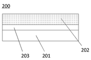
- the stacked body 200 shown in FIG. 2 is an example in which a stress relaxation layer 203 is provided as an intermediate layer between the crystal substrate 201 and the semiconductor film 202. This alleviates the lattice mismatch between the crystal substrate 201 and the semiconductor film 202 and increases the crystallinity of the semiconductor film 202, so that the electrical characteristics can be further improved.
- the stress relaxation layer 203 when an ⁇ -gallium oxide film is formed on an ⁇ -Al 2 O 3 substrate, the stress relaxation layer 203 includes ⁇ -Fe 2 O 3 , ⁇ -Ga 2 O 3 , ⁇ -Al 2 O 3 and A mixed crystal of these is preferably used.
- the lattice constant of the stress relaxation layer 203 is changed from a value close to or similar to that of the crystal substrate 201 toward a growth direction of the stress relaxation layer 203 to a value close to or similar to that of the semiconductor film 202. It is preferable to change continuously or stepwise. That is, it is preferable that the stress relaxation layer 203 be formed of (Al x Ga 1-x ) 2 O 3 (0 ⁇ x ⁇ 1) and the x value be decreased from the substrate 201 side toward the semiconductor 202 side.
- the method for forming the stress relaxation layer 203 is not particularly limited and may be a known method or the same as the method for forming the semiconductor film 202.
- the stress relaxation layer 203 may or may not contain a dopant.
- the semiconductor film according to the present invention is not only low in resistance but also excellent in electrical characteristics and is industrially useful. Such a semiconductor film can be suitably used for a semiconductor device and the like, and is particularly useful for a power device.
- the semiconductor film according to the present invention can be used as an n-type semiconductor layer (including an n + type semiconductor layer and an n ⁇ type semiconductor layer) of a semiconductor device.
- the laminate according to the present invention may be used as it is, or may be applied to a semiconductor device or the like after using a known means such as peeling a semiconductor film from a crystal substrate or the like.
- semiconductor devices should be classified into a horizontal element (horizontal device) having electrodes formed on one side of a semiconductor layer and a vertical element (vertical device) having electrodes on both front and back sides of the semiconductor layer.
- horizontal element horizontal device
- vertical element vertical device
- at least a part of the laminate according to the present invention can be suitably used for a horizontal device and a vertical device. In particular, it is preferably used for a vertical device.
- Examples of the semiconductor device include a Schottky barrier diode (SBD), a metal semiconductor field effect transistor (MESFET), a high electron mobility transistor (HEMT), a metal oxide semiconductor field effect transistor (MOSFET), and a junction field effect transistor ( JFET), an insulated gate bipolar transistor (IGBT), a light emitting element (light emitting diode, LED), or the like.
- SBD Schottky barrier diode
- MESFET metal semiconductor field effect transistor
- HEMT high electron mobility transistor
- MOSFET metal oxide semiconductor field effect transistor
- JFET junction field effect transistor
- IGBT insulated gate bipolar transistor
- LED light emitting element
- the laminated body or semiconductor film according to the present invention is applied to an n-type semiconductor (n + type semiconductor layer, n ⁇ semiconductor layer, etc.) to form a semiconductor device
- n-type semiconductor n + type semiconductor layer, n ⁇ semiconductor layer, etc.
- the semiconductor device illustrated below may further include other layers (for example, an insulator layer or a conductor layer) depending on the specifications or purposes, and may include an intermediate layer or a buffer layer (buffer layer). It goes without saying that ), etc. may be added or omitted as appropriate.
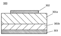
- FIG. 3 is an example of a Schottky barrier diode (SBD).
- the SBD 300 includes an n ⁇ type semiconductor layer 301a that is relatively lightly doped, an n + type semiconductor layer 301b that is relatively heavily doped, a Schottky electrode 302, and an ohmic electrode 303.
- the material of the Schottky electrode 302 and the ohmic electrode 303 may be a known electrode material, and examples of the electrode material include Al, Mo, Co, Zr, Sn, Nb, Fe, Cr, Ta, Ti, Au. , Pt, V, Mn, Ni, Cu, Hf, W, Ir, Zn, In, Pd, Nd or Ag, or alloys thereof, tin oxide, zinc oxide, rhenium oxide, indium oxide, indium tin oxide ( Examples thereof include a metal oxide conductive film such as ITO) and zinc indium oxide (IZO), an organic conductive compound such as polyaniline, polythiophene, and polypyrrole, a mixture thereof, and a laminated body.
- the electrode material include Al, Mo, Co, Zr, Sn, Nb, Fe, Cr, Ta, Ti, Au. , Pt, V, Mn, Ni, Cu, Hf, W, Ir, Zn, In, Pd, Nd or Ag, or alloys thereof
- the Schottky electrode 302 and the ohmic electrode 303 can be formed by a known means such as a vacuum vapor deposition method or a sputtering method. More specifically, for example, when a Schottky electrode is formed by using two kinds of the electrode materials (first metal and second metal), a layer made of the first metal and a second metal are used. It can be formed by stacking the layers made of, and patterning the layer made of the first metal and the layer made of the second metal using a photolithography technique.
- the SBD to which the laminated body or the semiconductor film according to the present invention is applied is excellent in high withstand voltage and large current, has a high switching speed, and has excellent withstand voltage and reliability.
- FIG. 4 is an example of a high electron mobility transistor (HEMT).
- the HEMT 400 includes an n-type semiconductor layer 401 having a wide bandgap, an n-type semiconductor layer 402 having a narrow bandgap, an n + type semiconductor layer 403, a semi-insulating layer 404, a buffer layer 405, a gate electrode 406, a source electrode 407, and a drain electrode. 408 is provided.
- FIG. 5 is an example of a metal oxide semiconductor field effect transistor (MOSFET).
- the MOSFET 500 includes an n ⁇ type semiconductor layer 501, n + type semiconductor layers 502 and 503, a gate insulating film 504, a gate electrode 505, a source electrode 506 and a drain electrode 507.
- FIG. 6 is an example of an insulated gate bipolar transistor (IGBT).
- the IGBT 600 includes an n-type semiconductor layer 601, an n ⁇ type semiconductor layer 602, an n + type semiconductor layer 603, a p type semiconductor layer 604, a gate insulating film 605, a gate electrode 606, an emitter electrode 607 and a collector electrode 608.
- FIG. 7 shows an example of a light emitting element (light emitting diode, LED).
- the LED 700 includes a first electrode 701, an n-type semiconductor layer 702, a light emitting layer 703, a p-type semiconductor layer 704, a translucent electrode 705, and a second electrode 706.
- a conductive material such as an oxide containing In or Ti can be given. More specifically, for example, In 2 O 3, ZnO, SnO 2, Ga 2 O 3, etc. TiO 2, CeO 2, or two or more of these mixed crystals or those doped thereof.
- the transparent electrode 705 can be formed by providing these materials by a known means such as sputtering. In addition, after forming the transparent electrode 705, thermal annealing may be performed for the purpose of making the transparent electrode 705 transparent.
- Examples of the material of the first electrode 701 and the second electrode 706 include Al, Mo, Co, Zr, Sn, Nb, Fe, Cr, Ta, Ti, Au, Pt, V, Mn, Ni, Cu, Metals such as Hf, W, Ir, Zn, In, Pd, Nd or Ag or alloys thereof, such as tin oxide, zinc oxide, rhenium oxide, indium oxide, indium tin oxide (ITO) and zinc indium oxide (IZO). Examples thereof include a metal oxide conductive film, an organic conductive compound such as polyaniline, polythiophene and polypyrrole, or a mixture thereof.
- the electrode film forming method is not particularly limited, and it is a wet method such as a printing method, a spray method, or a coating method, a physical method such as a vacuum deposition method, a sputtering method, an ion plating method, CVD, or plasma CVD. It can be formed by a method appropriately selected from chemical methods such as a method in consideration of compatibility with a material.
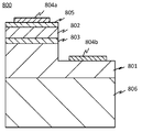
- a light-emitting element 800 in FIG. 8 includes an n-type semiconductor layer 801, a p-type semiconductor layer 802, a light-emitting layer 803, a light-transmitting electrode 805, a first electrode 804a, and part of the n-type semiconductor layer 801 over a substrate 806.
- the second electrode 804b is provided on a part of the exposed surface of the n-type semiconductor layer 801 that is exposed by notching.
- a part of the semiconductor devices exemplified above is used, for example, in a system using a power supply device.
- the power supply device can be manufactured by connecting the semiconductor device to a wiring pattern or the like using a known means.
- FIG. 9 shows an example of a power supply system.
- FIG. 9 configures a power supply system using a plurality of power supply devices and control circuits.
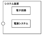
- the power supply system can be used as a system device in combination with an electronic circuit.
- FIG. 11 illustrates an example of a power supply circuit diagram of the power supply device.
- FIG. 11 shows a power supply circuit of a power supply device including a power circuit and a control circuit.
- the inverter MOSFET: composed of A to D
- the DCL smoothing coils L1 and L2
- the capacitor are smoothed to output a DC voltage.
- the voltage comparator compares the output voltage with the reference voltage, and the PWM control circuit controls the inverter and the rectifying MOSFET so that the desired output voltage is obtained.
- FIG. 12 shows an example of an apparatus used in the method for manufacturing a laminate according to the present invention.
- a mist CVD apparatus 900 is used as a film forming apparatus for forming a semiconductor film.
- the mist in the present invention refers to a general term for liquid fine particles dispersed in a gas, and includes what is called a mist, a droplet, or the like.
- the mist CVD apparatus 900 comprises a mist forming section 9A for forming a mist by forming a mist of a raw material solution, a carrier gas supply section 9B for supplying a carrier gas for carrying the mist, and a thermal reaction of the mist to form a mist on a substrate. It has a film forming unit 9C for forming a film, and a conveying unit 9D that connects the mist forming unit 9B and the film forming unit 9C and conveys the mist by the carrier gas.
- the film forming apparatus is characterized in that at least the surface of the transport section that comes into contact with the mist in the air-fuel mixture is made of a non-silicone resin.
- the inventors of the present invention who have found that Si in the semiconductor film is an obstacle to lowering the resistivity, have made earnest studies, and as a result, in the film forming apparatus, the raw materials have become mist and the film forming unit It was discovered that Si was incorporated into the semiconductor film by contacting with the components that make up the film forming apparatus before the reaction.
- the structure of the transport section 9D is not particularly limited, but it is easiest to use piping.
- the surface with which the mist contacts may be made of non-silicone resin. It is also possible to use a silicon-containing material such as a silicone-based resin on the outside and to use only the non-silicone-based resin on the inner surface that is in contact with the mist.
- the material of the transfer pipes 903 and 906 can be appropriately selected depending on the solvent of the precursor and the temperature in the reaction between the reactor and the transfer pipe as long as it is a non-silicone resin. Is.
- resin piping In the film forming apparatus according to the present invention, it is preferable to use resin piping.
- the resin pipe is flexible, and it is easy to handle and design the entire film forming apparatus.
- resin pipes include polyethylene, polypropylene, vinyl chloride, polystyrene, polyvinyl acetate, urethane resin, fluororesin, acrylonitrile butadiene styrene resin, acrylic resin, polyamide, polyimide, polyamideimide, nylon, acetal resin.
- Polycarbonate, polyphenylene ether, polyester, polyethylene terephthalate, polybutylene terephthalate, polyolefin, polyphenylene sulfide, polysulfone, polyether sulfone, polyarylate, and polyether ether ketone can be preferably used.
- the example of the transfer unit 9D illustrated in FIG. 12 has a structure in which the atomizer 902b and the film forming chamber 909 are connected by a transfer pipe 906, and the transfer pipe 903 from the atomizer 902a joins in the middle of the transfer pipe 906.
- the transfer pipe 903 and the transfer pipe 906 may be independently connected to the film forming chamber 909.
- the first air-fuel mixture and the second air-fuel mixture are introduced into a single buffer tank (not shown), and the mist mixed in the buffer tank is transferred to the film forming chamber 909 through the transfer pipe. May be.
- the mist forming unit 9A includes, for example, atomizers 902a and 902b, and the first precursor 912a and the second precursor 912b are stored in the atomizers 902a and 902b as raw material solutions, respectively.
- the first precursor 912a and the second precursor 912b include an organic metal complex of a metal (eg, acetylacetonate complex), an acid solution in which a metal is dissolved in an acid, or a halide (eg, fluoride, chloride, bromide). Or an aqueous solution of iodide).
- the metal is not limited as long as it can form a corundum structure as a metal oxide crystal, and examples thereof include Al, Ti, V, Cr, Fe, Ga, Rh, In, and Ir.
- the components of the first precursor 912a and the second precursor 912b may be the same or different. Further, the number of atomizers and the types of precursors can be increased or decreased depending on the composition of the film formed on the substrate and the laminated structure.
- the content of the metal in the raw material solution is not particularly limited and can be appropriately set according to the purpose and specifications. The amount is preferably 0.001 mol% to 50 mol%, more preferably 0.01 mol% to 5 mol%.
- the solvent of the raw material solution is not particularly limited, and may be an inorganic solvent such as water, an organic solvent such as alcohol, or a mixed solvent of an inorganic solvent and an organic solvent. Although good, it is preferable to use water.
- the impurity raw material used is not particularly limited.
- the metal contains at least Ga
- a complex or compound containing Si, Ge or Sn can be preferably used, and tin halide is particularly preferably used.
- These impurity raw materials can be used by mixing with 0.0001% to 20%, and more preferably 0.001% to 10% with respect to the metal element concentration in the raw material solution.
- the raw material solution is made into mist by using a mist forming means (also referred to as “atomization” or “droplet formation”) not shown.
- Mist formation of the raw material solution is not particularly limited as long as the raw material solution can be made into mist, but a mist forming means using ultrasonic waves is preferable.
- the mist obtained by using ultrasonic waves has a zero initial velocity and floats in the air, for example, it is a mist that can be transported in a state of floating in the space, instead of being sprayed like a spray. It is particularly suitable because it can suppress damage due to collision energy.
- the carrier gas supply unit 9B is a supply unit that supplies the carrier gas 901 for carrying the mist.
- the carrier gas 901 to be used is not particularly limited, and for example, in addition to air, oxygen, ozone, an inert gas such as nitrogen or argon, or a reducing gas such as hydrogen gas or forming gas is suitable. Used for.
- the type of carrier gas may be one type or two or more types.
- the carrier gas supply unit 9B is appropriately provided with pipes and the like connected to the mist forming unit 9A, and gas flow adjusting means such as valves 904 and 905.
- the flow rate of the diluting gas may be set appropriately, and can be set to 0.1 to 10 times/minute that of the carrier gas.
- the diluent gas may be supplied to the downstream side of the atomizers 902a and 902b, for example.
- the diluent gas may be the same as the carrier gas or different from it.
- the film forming unit 9C includes a film forming chamber 909 having a susceptor 908 inside.
- the structure of the film forming chamber 909 is not particularly limited, and a metal such as aluminum or stainless steel may be used. If a film is formed at a higher temperature than the heat resistant temperature of these metals, quartz or Silicon carbide may be used.
- a heating means 910 for heating the crystal substrate 907 is provided inside or outside the film formation chamber 909. Further, the substrate 907 may be placed on the susceptor 908 installed in the film forming chamber 909.
- a film forming method comprises a step of forming an air-fuel mixture containing at least a misted metal oxide precursor, a carrier gas and a dopant, and the air-fuel mixture is conveyed to a film forming section via a conveying section. And a step of thermally reacting the air-fuel mixture in the film forming unit to form a semiconductor film on a substrate, at least a surface of the transfer unit in contact with the air-fuel mixture is made of a non-silicone resin. It is characterized by
- the raw material solution is made into mist in the mist forming section 9A using a known means to form mist.
- the size of the mist is not particularly limited and may be a droplet of about several mm, but is preferably 50 ⁇ m or less, more preferably 0.1 to 10 ⁇ m.
- the carrier gas supplied from the carrier gas supply unit to the mist forming unit 9A is mixed with the mistified raw material solution (precursor) formed in the atomizers 902a and 902b to form a gas mixture.
- the flow rate of the carrier gas may be appropriately set depending on the size of the substrate and the size of the film forming chamber, and can be set to about 0.01 to 40 L/min.
- the film formation may be carried out under atmospheric pressure, under pressure or under reduced pressure, but it is preferably carried out under atmospheric pressure in view of apparatus cost and productivity.
- the air-fuel mixture containing mist is transported via the transport unit 9D that connects the mist forming unit 9A and the film forming unit 9C. At this time, since the surface of the transport unit that contacts the air-fuel mixture is made of non-silicone resin, the mixing of Si into the mist in the air-fuel mixture is suppressed.
- the air-fuel mixture containing mist supplied to the film forming chamber 909 of the film forming unit 9C reacts on the crystal substrate 907 heated by the heat source 910 in the film forming chamber 909 to form a semiconductor film having a corundum structure. ..
- the substrate temperature at this time should be appropriately determined depending on the type of film formed on the substrate. For example, when forming an ⁇ -gallium oxide film, it is preferably 350° C. or higher and 950° C. or lower. Within such a range, a semiconductor film having higher crystallinity can be obtained.
- the film thickness can be set by adjusting the film formation time, the spray amount of the precursor, and the carrier gas flow rate.
- a stress relaxation layer is further formed between the semiconductor layer and the substrate, first, a first gas mixture is formed in which the carrier gas 901 and the atomized first precursor formed by the atomizer 902a are mixed, Further, the carrier gas 901 and the atomized second precursor formed by the atomizer 902b are mixed to form a second air-fuel mixture.
- the first air-fuel mixture and the second air-fuel mixture are transferred onto the crystal substrate 907 placed on the susceptor 908 in the film forming chamber 909 and heated by the heating means 910, so that the precursor reacts on the substrate surface.
- a semiconductor having a corundum structure in which the components of the first precursor and the components of the second precursor are mixed is formed.
- both or one of the carrier gas flow rates of the first air-fuel mixture and the second air-fuel mixture may be changed discretely or continuously over a predetermined time.
- the stress relaxation layer is formed of (Al x Ga 1-x ) 2 O 3 (0 ⁇ x ⁇ 1), and the substrate is grown from the growth side.
- the Al supply amount is set to be relatively larger than the Ga supply amount.
- the precursor concentration and carrier gas flow rate are adjusted.
- the first film formation is performed by using an air-fuel mixture using an Al-Ga precursor in which an Al source and a Ga source are mixed at a certain ratio, and thereafter, a plurality of Al concentrations are reduced in relative steps.
- a multilayer film of (Al x Ga 1-x ) 2 O 3 in which the Al composition is reduced stepwise may be formed by repeating stacking using an Al—Ga precursor.
- the substrate temperature at this time should be appropriately determined according to the type of film formed on the substrate. For example, when forming an (Al x Ga 1-x ) 2 O 3 (0 ⁇ x ⁇ 1) film It is preferable that the temperature is 350° C. or higher and 950° C. or lower. Within such a range, a semiconductor film having higher crystallinity can be obtained.
- the film thickness can be set by adjusting the film formation time.
- Example 1 In the film forming apparatus of FIG. 12, using only one atomizer, ⁇ -gallium oxide film was formed by the following procedure. First, an aqueous solution of gallium acetylacetonate was prepared so that the Ga concentration was 0.10 mol/L. To this aqueous solution, tin(II) chloride was added so that the atomic ratio of Sn to Ga concentration was 1:0.005, and 1.0% by volume of hydrochloric acid was added, and this was used as a raw material solution. did. This raw material solution was filled in an atomizer.
- a ⁇ -(Al x Ga 1-x ) 2 O 3 multilayer film (non-doped, 0.02 ⁇ x ⁇ 0.2) is formed on the surface as a buffer layer and has a diameter of 2 inches (50 mm).
- the sapphire substrate was placed on a quartz susceptor and placed in a quartz tubular film forming chamber, and the substrate temperature was kept at 430° C. by a heater.
- the raw material solution in the atomizer was atomized with a 2.4 MHz ultrasonic transducer. Then, nitrogen as a carrier gas was introduced into the atomizer at 1.0 L/min and nitrogen as a diluent gas was introduced at 0.5 L/min to form a mixture gas, and a carrier pipe made of polytetrafluoroethylene ( It was supplied to a film forming chamber through a PTFE tube) and film formation was carried out under atmospheric pressure for 60 minutes to form an ⁇ -gallium oxide film having a film thickness of 3.5 ⁇ m.
- the substrate was cooled to room temperature and then taken out from the film forming chamber, and the carrier concentration, the resistivity and the mobility were measured by the Van der Pauw method (accent HL5500). Further, the Si concentration in the film was measured by SIMS (CAMECA IMS-7f). The detection limit of Si in this measurement is 5 ⁇ 10 14 cm ⁇ 3 .
- Example 2 An ⁇ -gallium oxide film having a thickness of 3.5 ⁇ m was formed in the same manner as in Example 1 except that the air-fuel mixture conveying pipe was made of vinyl chloride. After that, the substrate was cooled to room temperature and then taken out from the film forming chamber, and the carrier concentration, the resistivity, the mobility, and the Si concentration in the film were measured in the same manner as in Example 1.
- Example 3 An ⁇ -gallium oxide film having a thickness of 3.5 ⁇ m was formed in the same manner as in Example 1 except that the air-fuel mixture conveying pipe was made of polyethylene. After that, the substrate was cooled to room temperature and then taken out from the film forming chamber, and the carrier concentration, the resistivity, the mobility, and the Si concentration in the film were measured in the same manner as in Example 1.
- Example 4 An ⁇ -gallium oxide film having a film thickness of 3.5 ⁇ m was formed in the same manner as in Example 1 except that the air-fuel mixture conveying pipe was made of urethane resin. Then, the substrate was cooled to room temperature and then taken out from the film forming chamber, and the carrier concentration, resistivity, mobility and Si concentration in the film were measured in the same manner as in Example 1.
- Example 5 As a raw material solution, gallium chloride was added to an aqueous solution adjusted to have a Ga concentration of 0.10 mol/L, and germanium oxide was added so that the atomic ratio of Ge as a dopant to the Ga concentration was 1:0.005. Then, a film was formed in the same manner as in Example 1 except that hydrochloric acid was added in an amount of 1.0% by volume to form an ⁇ -gallium oxide film having a thickness of 2.0 ⁇ m. After that, the substrate was cooled to room temperature and then taken out from the film forming chamber, and the carrier concentration, the resistivity, the mobility, and the Si concentration in the film were measured in the same manner as in Example 1.
- Example 1 An ⁇ -gallium oxide film having a film thickness of 3.5 ⁇ m was formed in the same manner as in Example 1 except that the air-fuel mixture conveying pipe was made of silicone resin. After that, the substrate was cooled to room temperature and then taken out from the film forming chamber, and the carrier concentration, resistivity, mobility, and Si concentration in the film were measured in the same manner as in Example 1.
- Example 2 An ⁇ -gallium oxide film having a thickness of 2.0 ⁇ m was formed in the same manner as in Example 5 except that the air-fuel mixture conveying pipe was made of silicone resin. After that, the substrate was cooled to room temperature and then taken out from the film forming chamber, and the carrier concentration, resistivity, mobility, and Si concentration in the film were measured in the same manner as in Example 1.
- Table 1 shows the carrier density, mobility and resistivity of the ⁇ -gallium oxide films obtained in Examples 1-5 and Comparative Examples 1-2.
- Si was not detected (below the detection limit) and the resistivity was about 4 m ⁇ cm, which was extremely low as compared with the comparative example. It was possible to obtain a carrier having a high carrier concentration and high mobility and excellent electric characteristics.
- the present invention is not limited to the above embodiment.
- the above-described embodiment is an exemplification, and the invention having substantially the same configuration as the technical idea described in the scope of the claims of the present invention and exhibiting the same operation effect is not limited to the present invention.
Landscapes
- Chemical & Material Sciences (AREA)
- Engineering & Computer Science (AREA)
- General Chemical & Material Sciences (AREA)
- Chemical Kinetics & Catalysis (AREA)
- Materials Engineering (AREA)
- Mechanical Engineering (AREA)
- Metallurgy (AREA)
- Organic Chemistry (AREA)
- Inorganic Chemistry (AREA)
- Chemical Vapour Deposition (AREA)
- Liquid Deposition Of Substances Of Which Semiconductor Devices Are Composed (AREA)
- Ceramic Engineering (AREA)
- Crystallography & Structural Chemistry (AREA)
- Crystals, And After-Treatments Of Crystals (AREA)
- Thin Film Transistor (AREA)
- Manufacturing Of Printed Wiring (AREA)
- Internal Circuitry In Semiconductor Integrated Circuit Devices (AREA)
Abstract
Description
図1は、本発明に係る積層体の一形態を示す図である。積層体100は結晶基板101と、結晶基板101上に直接形成された半導体膜102を備える。
半導体膜102は、コランダム構造を有する酸化物半導体を主成分として含み、さらにドーパントを含む酸化物半導体膜であって、Si濃度が5.0×1020cm-3以下、より好ましくは3.0×1020cm-3以下であり、抵抗率が150m・Ωcm以下、より好ましくは20m・Ωcm以下であるのがよい。なお、「酸化物半導体を主成分とし」との表現においては、酸化物半導体のほかに、ドーパントや不可避的不純物等が含まれていてもよいことを意味しており、例えば、酸化物半導体が概ね50%以上含まれているものを指す。なお、Si濃度の下限値は0であるが、1×1016cm-3とすることもできる。また、前記抵抗率の下限値は特に限定されないが、例えば、1.0×10⁻¹m・Ωcmとすることができる。
一方、基板101は、その上にコランダム構造を有する酸化物半導体膜が形成できる結晶基板であれば、特に限定されない。主面の全部又は一部にコランダム構造を有している基板を用いることが好ましい。結晶成長面側の主面の全部又は一部にコランダム構造を有している基板であるのがより好ましく、結晶成長面側の主面の全部にコランダム構造を有している基板であればさらに好ましい。具体的には、α-Al2O3(サファイア基板)又はα-酸化ガリウムが好適に用いられる。また、本発明においては、前記主面がc面であれば、より電気特性を向上させることができるので好ましい。また、基板101は、主面の結晶面がオフ角を有していてもよい。この場合、一般的にオフ角を0.1°~10.0°とするのが良い。
図12に、本発明に係る積層体の製造方法に用いる装置の一例を示す。本発明に係る積層体の製造において、半導体膜の成膜には、成膜装置としてミストCVD装置900を用いる。
まず、ミスト化部9Aと成膜部9Cとを接続する搬送部9Dについて説明する。本発明に係る成膜装置においては、搬送部の、少なくとも混合気中のミストと接触する面が非シリコーン系樹脂とされる点に特徴を有する。上述のように、半導体膜中のSiが低抵抗率化の障害となっていることを見出した本発明者が鋭意検討を行った結果、成膜装置において、原料がミスト化され、成膜部で反応するまでの間に、成膜装置を構成する部品と接触することで、半導体膜中にSiを取り込んでいることを発見した。そこで、ミスト化部9Aと成膜部9Cとを接続する搬送部9Dにおける、混合気中のミストが接触する面(部分)を、Si非含有材料、特に、非シリコーン系樹脂とすることで、半導体膜の成膜を行ったときにSiの取り込みを抑制できることを見出した。
ミスト化部9Aは、例えば、霧化器902a、902bを備え霧化器902a、902b内には、原料溶液として、それぞれ、第1前駆体912a、第2前駆体912bが収納されている。第1前駆体912a、第2前駆体912bとしては、例えば、金属の有機金属錯体(例えばアセチルアセトナート錯体等)や金属を酸に溶解した酸溶液又はハロゲン化物(例えばフッ化物、塩化物、臭化物又はヨウ化物等)の水溶液などが挙げられる。前記金属は、金属酸化物結晶としてコランダム構造を形成可能な金属であれば限定されず、例えば、Al、Ti、V、Cr、Fe、Ga、Rh、In、Irが挙げられる。また、第1前駆体912aと第2前駆体912bの成分は、同一でもよいし異なっていてもよい。さらに、霧化器の数及び前駆体の種類は、基板上に形成する膜の組成や積層構造に応じて増減させることができる。原料溶液中の金属の含有量は、特に限定されず、目的や仕様に応じて適宜設定できる。好ましくは、0.001モル%~50モル%であり、より好ましくは0.01モル%~5モル%である。
キャリアガス供給部9Bは、ミストを搬送するためのキャリアガス901の供給を行う供給手段である。キャリアガス供給部9Bにおいて、使用するキャリアガス901は、特に限定されず、例えば、空気、酸素、オゾンの他、窒素やアルゴン等の不活性ガス、又は水素ガスやフォーミングガス等の還元ガスが好適に用いられる。キャリアガスの種類は1種類であっても、2種類以上であってもよい。なお、キャリアガス供給部9Bには、ミスト化部9Aに接続する配管等や、バルブ904、905等のガス流調整手段が適宜設けられている。
成膜部9Cは、内部にサセプタ908を有する成膜室909を備えている。成膜室909の構造等は特に限定されるものではなく、アルミニウムやステンレスなどの金属を用いて良いし、これらの金属の耐熱温度を超える、より高温で成膜を行う場合には、石英や炭化シリコンを用いても良い。成膜室909の内部又は外部には、結晶基板907を加熱するための加熱手段910が設けられている。また、基板907は成膜室909内に設置されたサセプタ908上に載置されてよい。
本発明に係る成膜方法は、少なくともミスト化した金属酸化物前駆体とキャリアガスとドーパントを含む混合気を形成するステップと、前記混合気を、搬送部を経由して成膜部へ搬送するステップと、前記成膜部で前記混合気を熱反応させて、基板上に半導体膜を形成するステップとを含み、少なくとも前記搬送部における前記混合気と接触する面を、非シリコーン系樹脂とすることを特徴としている。
まず、原料溶液はミスト化部9Aにおいて公知の手段を用いてミスト化され、ミストが形成される。ミストのサイズは、特に限定されず、数mm程度の液滴であってもよいが、好ましくは50μm以下であり、より好ましくは0.1~10μmである。
ミストを含む混合気は、ミスト化部9Aと成膜部9Cとを接続する搬送部9Dを介して、搬送される。このとき、搬送部における混合気と接触する面が、非シリコーン系樹脂とされているため、混合気中のミストへのSiの混入が抑制される。
成膜部9Cの成膜室909に供給されたミストを含む混合気は、成膜室909内で熱源910により加熱された結晶基板907上で反応し、コランダム構造を有する半導体膜が形成される。この時の基板温度は、基板上に形成する膜種によって適宜決定されるべきであるが、例えばα-酸化ガリウム膜を形成する場合、350℃以上950℃以下とするのが良い。このような範囲であれば、より結晶性の高い半導体膜を得ることができる。なお、膜厚は、成膜時間や前駆体の噴霧量及びキャリアガス流量を調整することにより設定することができる。
半導体層と基板の間に、さらに応力緩和層を形成する場合は、まず、キャリアガス901と霧化器902aで形成した霧化した第1前駆体が混合された第1混合気を形成し、さらにキャリアガス901と霧化器902bで形成した霧化した第2前駆体が混合された第2混合気を形成する。
図12の成膜装置において、1台の霧化器のみを用い、以下の手順でα-酸化ガリウムの成膜を行った。まずガリウムアセチルアセトナートを、Ga濃度が0.10モル/Lとなるように水溶液を調整した。この水溶液に、Ga濃度に対するSnの原子比が1:0.005となるように塩化スズ(II)を添加し、さらに塩酸を体積比で1.0%を添加して、これを原料溶液とした。この原料溶液を霧化器に充填した。
混合気の搬送配管を塩化ビニル製にした以外は実施例1と同様にして、膜厚3.5μmのα-酸化ガリウム膜を形成した。この後、基板を室温まで冷却してから成膜室より取り出し、実施例1と同様にキャリア濃度、抵抗率、移動度、及び、膜中のSi濃度を測定した。
混合気の搬送配管をポリエチレン製にした以外は実施例1と同様にして、膜厚3.5μmのα-酸化ガリウム膜を形成した。この後、基板を室温まで冷却してから成膜室より取り出し、実施例1と同様にキャリア濃度、抵抗率、移動度、及び、膜中のSi濃度を測定した。
混合気の搬送配管をウレタン樹脂製にした以外は実施例1と同様にして、膜厚3.5μmのα-酸化ガリウム膜を形成した。この後、基板を室温まで冷却してから成膜室より取り出し、実施例1と同様にキャリア濃度、抵抗率、移動度、及び、膜中のSi濃度を測定した。
原料溶液として、塩化ガリウムを、Ga濃度が0.10モル/Lとなるように調整した水溶液に、Ga濃度に対するドーパントであるGeの原子比が1:0.005となるように酸化ゲルマニウムを添加し、さらに塩酸を体積比で1.0%を添加したものを用いたこと以外は実施例1と同様にして成膜を行い、膜厚2.0μmのα-酸化ガリウム膜を形成した。この後、基板を室温まで冷却してから成膜室より取り出し、実施例1と同様にキャリア濃度、抵抗率、移動度、及び、膜中のSi濃度を測定した。
混合気の搬送配管をシリコーン樹脂製にした以外は実施例1と同様にして、膜厚3.5μmのα-酸化ガリウム膜を形成した。この後、基板を室温まで冷却してから成膜室より取り出し、実施例1と同様にキャリア濃度、抵抗率、移動度、及び膜中のSi濃度を測定した。
混合気の搬送配管をシリコーン樹脂製にした以外は実施例5と同様にして、膜厚2.0μmのα-酸化ガリウム膜を形成した。この後、基板を室温まで冷却してから成膜室より取り出し、実施例1と同様にキャリア濃度、抵抗率、移動度、及び膜中のSi濃度を測定した。

Claims (15)
- 結晶基板と
該結晶基板の主表面上に設けられ、ドーパントを含有しコランダム構造を有する酸化物半導体を主成分として含む半導体膜とを含む積層体であって、
前記酸化物半導体に含まれるSi濃度が5.0×1020cm-3以下であり、前記半導体膜の抵抗率が150mΩ・cm以下であることを特徴とする積層体。 - 前記半導体膜の抵抗率が20mΩ・cm以下であることを特徴とする請求項1に記載の積層体。
- 前記半導体膜の主面がc面であることを特徴とする請求項1又は2に記載の積層体。
- 前記ドーパントがSn、Ge又はSiから選択される少なくとも1つであることを特徴とする請求項1から3のいずれか一項に記載の積層体。
- 前記ドーパントがSnであることを特徴とする請求項1から4のいずれか一項に記載の積層体。
- 前記半導体膜におけるキャリア移動度が20cm2/Vs以上であることを特徴とする請求項1から5のいずれか一項に記載の積層体。
- 前記半導体膜におけるキャリア密度が1.0×10¹⁸/cm3以上であることを特徴とする請求項1から6のいずれか一項に記載の積層体。
- 前記酸化物半導体がGa、In又はAlを含むものであることを特徴とする請求項1から7のいずれか一項に記載の積層体。
- 前記酸化物半導体が少なくともGaを含むものであることを特徴とする請求項1から8のいずれか一項に記載の積層体。
- 半導体と電極とを少なくとも含む半導体装置であって、前記半導体として請求項1から9のいずれか一項に記載の積層体の少なくとも一部を備えることを特徴とする半導体装置。
- 半導体システムであって、請求項10に記載の半導体装置を含むことを特徴とする半導体システム。
- 少なくともミスト化した金属酸化物前駆体とキャリアガスとドーパントを含む混合気を形成するステップと、
前記混合気を、搬送部を経由して成膜部へ搬送するステップと、
前記成膜部で前記混合気を熱反応させて、基板上に半導体膜を形成するステップとを含む成膜方法であって、
少なくとも前記搬送部における前記混合気と接触する面を、非シリコーン系樹脂とすることを特徴とする成膜方法。 - 前記非シリコーン系樹脂は、ポリエチレン、ポリプロピレン、塩化ビニル、ポリスチレン、ポリ酢酸ビニル、ウレタン樹脂、フッ素樹脂、アクリロニトリルブタジエンスチレン樹脂、アクリル樹脂、ポリアミド、ポリイミド、ポリアミドイミド、ナイロン、アセタール樹脂、ポリカーボネート、ポリフェニレンエーテル、ポリエステル、ポリエチレンテレフタレート、ポリブチレンテレフタレート、ポリオレフィン、ポリフェニレンサルファイド、ポリサルフォン、ポリエーテルサルフォン、ポリアリレート、ポリエーテルエーテルケトンのいずれか1つ以上を含むものであることを特徴とする請求項12に記載の成膜方法。
- 前記非シリコーン系樹脂はフッ素樹脂を含むものであることを特徴とする請求項12又は13に記載の成膜方法。
- 原料溶液をミスト化してミストを発生させるミスト化部と、
前記ミストを搬送するキャリアガスを供給するキャリアガス供給部と、
前記ミストを熱反応させて基板上に成膜を行う成膜部と、
前記ミスト化部と前記成膜部とを接続し、前記キャリアガスによって前記ミストが搬送される搬送部とを有する成膜装置であって、
前記搬送部は、少なくとも前記ミストと接触する面が非シリコーン系樹脂とされているものであることを特徴とする成膜装置。
Priority Applications (5)
| Application Number | Priority Date | Filing Date | Title |
|---|---|---|---|
| CN201980082989.6A CN113243043B (zh) | 2018-12-19 | 2019-11-18 | 层叠体、成膜方法及成膜装置 |
| EP19898090.6A EP3901994B1 (en) | 2018-12-19 | 2019-11-18 | MULTILAYER BODY, FILM FORMING METHOD AND FILM FORMING APPARATUS |
| US17/414,073 US12074078B2 (en) | 2018-12-19 | 2019-11-18 | Laminate, film forming method, and film forming apparatus |
| KR1020217017796A KR102705141B1 (ko) | 2018-12-19 | 2019-11-18 | 적층체, 성막 방법 및 성막 장치 |
| US18/767,382 US20240363468A1 (en) | 2018-12-19 | 2024-07-09 | Laminate, film forming method, and film forming apparatus |
Applications Claiming Priority (2)
| Application Number | Priority Date | Filing Date | Title |
|---|---|---|---|
| JP2018236960A JP6857641B2 (ja) | 2018-12-19 | 2018-12-19 | 成膜方法及び成膜装置 |
| JP2018-236960 | 2018-12-19 |
Related Child Applications (2)
| Application Number | Title | Priority Date | Filing Date |
|---|---|---|---|
| US17/414,073 A-371-Of-International US12074078B2 (en) | 2018-12-19 | 2019-11-18 | Laminate, film forming method, and film forming apparatus |
| US18/767,382 Continuation US20240363468A1 (en) | 2018-12-19 | 2024-07-09 | Laminate, film forming method, and film forming apparatus |
Publications (1)
| Publication Number | Publication Date |
|---|---|
| WO2020129508A1 true WO2020129508A1 (ja) | 2020-06-25 |
Family
ID=71100448
Family Applications (1)
| Application Number | Title | Priority Date | Filing Date |
|---|---|---|---|
| PCT/JP2019/045034 Ceased WO2020129508A1 (ja) | 2018-12-19 | 2019-11-18 | 積層体、成膜方法及び成膜装置 |
Country Status (7)
| Country | Link |
|---|---|
| US (2) | US12074078B2 (ja) |
| EP (1) | EP3901994B1 (ja) |
| JP (2) | JP6857641B2 (ja) |
| KR (1) | KR102705141B1 (ja) |
| CN (1) | CN113243043B (ja) |
| TW (1) | TWI821483B (ja) |
| WO (1) | WO2020129508A1 (ja) |
Cited By (3)
| Publication number | Priority date | Publication date | Assignee | Title |
|---|---|---|---|---|
| WO2022004279A1 (ja) * | 2020-06-29 | 2022-01-06 | 信越化学工業株式会社 | 成膜用ドーピング原料溶液の製造方法、積層体の製造方法、成膜用ドーピング原料溶液及び半導体膜 |
| JP2022013622A (ja) * | 2020-06-29 | 2022-01-18 | 信越化学工業株式会社 | 成膜用ドーピング原料溶液の製造方法、積層体の製造方法、成膜用ドーピング原料溶液及び半導体膜 |
| JP2023156732A (ja) * | 2022-04-13 | 2023-10-25 | 信越化学工業株式会社 | 結晶性積層構造体、半導体装置及び結晶性積層構造体の製造方法 |
Families Citing this family (18)
| Publication number | Priority date | Publication date | Assignee | Title |
|---|---|---|---|---|
| WO2021064795A1 (ja) * | 2019-09-30 | 2021-04-08 | 日本碍子株式会社 | α-Ga2O3系半導体膜 |
| WO2021157719A1 (ja) * | 2020-02-07 | 2021-08-12 | 株式会社Flosfia | 半導体素子および半導体装置 |
| JP2021172552A (ja) * | 2020-04-24 | 2021-11-01 | 株式会社Flosfia | 結晶膜 |
| US11694894B2 (en) * | 2020-04-24 | 2023-07-04 | Flosfia Inc. | Crystalline film containing a crystalline metal oxide and method for manufacturing the same under partial pressure |
| JP7311464B2 (ja) * | 2020-06-05 | 2023-07-19 | 株式会社平和 | 遊技機 |
| JP7311466B2 (ja) * | 2020-06-05 | 2023-07-19 | 株式会社平和 | 遊技機 |
| KR20230048008A (ko) * | 2020-08-06 | 2023-04-10 | 신에쓰 가가꾸 고교 가부시끼가이샤 | 반도체 적층체, 반도체 소자 및 반도체 소자의 제조방법 |
| JP7061214B2 (ja) * | 2020-08-06 | 2022-04-27 | 信越化学工業株式会社 | 半導体積層体、半導体素子および半導体素子の製造方法 |
| JP7678955B2 (ja) * | 2020-08-07 | 2025-05-19 | 株式会社Flosfia | p型酸化物半導体及びp型酸化物半導体を含む半導体装置 |
| WO2022030648A2 (ja) * | 2020-08-07 | 2022-02-10 | 株式会社Flosfia | p型酸化物半導体及びp型酸化物半導体を含む半導体装置 |
| JP2022030646A (ja) * | 2020-08-07 | 2022-02-18 | 株式会社Flosfia | 酸化物半導体及び酸化物半導体を含む半導体装置 |
| JP7531155B2 (ja) * | 2020-12-25 | 2024-08-09 | 株式会社デンソー | 酸化膜を有する製品の製造方法 |
| US20220223696A1 (en) * | 2021-01-13 | 2022-07-14 | Electronics And Telecommunications Research Institute | Method for manufacturing power semiconductor device |
| JPWO2022230832A1 (ja) * | 2021-04-26 | 2022-11-03 | ||
| JP2023056328A (ja) * | 2021-10-07 | 2023-04-19 | 信越化学工業株式会社 | 成膜装置およびこれを用いた結晶性半導体膜の成膜方法 |
| JP2023141340A (ja) | 2022-03-23 | 2023-10-05 | キオクシア株式会社 | 半導体装置の製造方法 |
| WO2025203519A1 (ja) * | 2024-03-28 | 2025-10-02 | 日本碍子株式会社 | 半導体膜、複合膜、及び半導体膜付き下地基板 |
| CN119698033A (zh) * | 2024-12-06 | 2025-03-25 | 西安电子科技大学 | 金刚石基氧化镓mosfet器件及其制作方法 |
Citations (4)
| Publication number | Priority date | Publication date | Assignee | Title |
|---|---|---|---|---|
| JP2013028480A (ja) | 2011-07-27 | 2013-02-07 | Kochi Univ Of Technology | ドーパントを添加した結晶性の高い導電性α型酸化ガリウム薄膜およびその生成方法 |
| JP2015228495A (ja) | 2014-05-08 | 2015-12-17 | 株式会社Flosfia | 結晶性積層構造体、半導体装置 |
| JP2018070422A (ja) * | 2016-11-01 | 2018-05-10 | 国立大学法人 和歌山大学 | 酸化ガリウムの製造方法及び結晶成長装置 |
| JP2018082144A (ja) * | 2016-08-31 | 2018-05-24 | 株式会社Flosfia | 結晶性酸化物半導体膜および半導体装置 |
Family Cites Families (4)
| Publication number | Priority date | Publication date | Assignee | Title |
|---|---|---|---|---|
| JP2006143996A (ja) | 2004-10-19 | 2006-06-08 | Nitto Denko Corp | 耐熱性樹脂 |
| JP5343224B1 (ja) | 2012-09-28 | 2013-11-13 | Roca株式会社 | 半導体装置および結晶 |
| JP5397795B1 (ja) * | 2013-06-21 | 2014-01-22 | Roca株式会社 | 半導体装置及びその製造方法、結晶及びその製造方法 |
| US10804362B2 (en) | 2016-08-31 | 2020-10-13 | Flosfia Inc. | Crystalline oxide semiconductor film, crystalline oxide semiconductor device, and crystalline oxide semiconductor system |
-
2018
- 2018-12-19 JP JP2018236960A patent/JP6857641B2/ja active Active
-
2019
- 2019-11-18 EP EP19898090.6A patent/EP3901994B1/en active Active
- 2019-11-18 KR KR1020217017796A patent/KR102705141B1/ko active Active
- 2019-11-18 US US17/414,073 patent/US12074078B2/en active Active
- 2019-11-18 CN CN201980082989.6A patent/CN113243043B/zh active Active
- 2019-11-18 WO PCT/JP2019/045034 patent/WO2020129508A1/ja not_active Ceased
- 2019-12-18 TW TW108146379A patent/TWI821483B/zh active
-
2021
- 2021-03-22 JP JP2021047355A patent/JP7135145B2/ja active Active
-
2024
- 2024-07-09 US US18/767,382 patent/US20240363468A1/en active Pending
Patent Citations (4)
| Publication number | Priority date | Publication date | Assignee | Title |
|---|---|---|---|---|
| JP2013028480A (ja) | 2011-07-27 | 2013-02-07 | Kochi Univ Of Technology | ドーパントを添加した結晶性の高い導電性α型酸化ガリウム薄膜およびその生成方法 |
| JP2015228495A (ja) | 2014-05-08 | 2015-12-17 | 株式会社Flosfia | 結晶性積層構造体、半導体装置 |
| JP2018082144A (ja) * | 2016-08-31 | 2018-05-24 | 株式会社Flosfia | 結晶性酸化物半導体膜および半導体装置 |
| JP2018070422A (ja) * | 2016-11-01 | 2018-05-10 | 国立大学法人 和歌山大学 | 酸化ガリウムの製造方法及び結晶成長装置 |
Non-Patent Citations (2)
| Title |
|---|
| CHIKOIDZE, E. ET AL.: "Electrical, optical, and magnetic properties of Sn doped a-Ga 0 thin films", JOURNAL OF APPLIED PHYSICS, vol. 120.2, 2016, pages 025109 |
| KAZUAKI AKAIWA, FUJITA SHIZUO: "Electrical Conductive Corundum- Structured alpha-Ga203 Thin Films on Sapphire with Tin-Doping Grown by Spray- Assisted Mist Chemical Vapor Deposition", THE JAPANESE JOURNAL OF APPLIED PHYSICS, vol. 51, 14 June 2012 (2012-06-14), pages 1 - 3, XP055204013, DOI: 10.1143/jjap.51.070203 * |
Cited By (4)
| Publication number | Priority date | Publication date | Assignee | Title |
|---|---|---|---|---|
| WO2022004279A1 (ja) * | 2020-06-29 | 2022-01-06 | 信越化学工業株式会社 | 成膜用ドーピング原料溶液の製造方法、積層体の製造方法、成膜用ドーピング原料溶液及び半導体膜 |
| JP2022013622A (ja) * | 2020-06-29 | 2022-01-18 | 信越化学工業株式会社 | 成膜用ドーピング原料溶液の製造方法、積層体の製造方法、成膜用ドーピング原料溶液及び半導体膜 |
| JP7011207B2 (ja) | 2020-06-29 | 2022-01-26 | 信越化学工業株式会社 | 成膜用ドーピング原料溶液の製造方法、積層体の製造方法、成膜用ドーピング原料溶液及び半導体膜 |
| JP2023156732A (ja) * | 2022-04-13 | 2023-10-25 | 信越化学工業株式会社 | 結晶性積層構造体、半導体装置及び結晶性積層構造体の製造方法 |
Also Published As
| Publication number | Publication date |
|---|---|
| CN113243043B (zh) | 2025-03-25 |
| JP2021101482A (ja) | 2021-07-08 |
| JP7135145B2 (ja) | 2022-09-12 |
| TW202035772A (zh) | 2020-10-01 |
| JP6857641B2 (ja) | 2021-04-14 |
| JP2020098875A (ja) | 2020-06-25 |
| EP3901994A4 (en) | 2022-09-14 |
| US20220059424A1 (en) | 2022-02-24 |
| KR20210103474A (ko) | 2021-08-23 |
| US20240363468A1 (en) | 2024-10-31 |
| EP3901994B1 (en) | 2025-12-31 |
| KR102705141B1 (ko) | 2024-09-09 |
| TWI821483B (zh) | 2023-11-11 |
| CN113243043A (zh) | 2021-08-10 |
| EP3901994A1 (en) | 2021-10-27 |
| US12074078B2 (en) | 2024-08-27 |
Similar Documents
| Publication | Publication Date | Title |
|---|---|---|
| JP7135145B2 (ja) | 半導体膜、成膜方法及び成膜装置 | |
| KR102329576B1 (ko) | p형 산화물 반도체 및 그 제조 방법 | |
| KR102467802B1 (ko) | 산화물 반도체 막 및 그 제조 방법 | |
| JP6994181B2 (ja) | 結晶性酸化物半導体膜および半導体装置 | |
| JP7220257B2 (ja) | 積層体、半導体装置、ミストcvd装置及び成膜方法 | |
| JP7391290B2 (ja) | 結晶性酸化物半導体膜および半導体装置 | |
| JP7358718B2 (ja) | 結晶性酸化物半導体膜および半導体装置 | |
| JP7065443B2 (ja) | p型酸化物半導体及びその製造方法 | |
| JP2023169231A (ja) | 半導体積層体 | |
| WO2022030647A2 (ja) | 酸化物半導体及び酸化物半導体を含む半導体装置 | |
| JP7053539B2 (ja) | 積層体、半導体膜、半導体装置、半導体システム及び積層体の製造方法 | |
| JP7061214B2 (ja) | 半導体積層体、半導体素子および半導体素子の製造方法 |
Legal Events
| Date | Code | Title | Description |
|---|---|---|---|
| 121 | Ep: the epo has been informed by wipo that ep was designated in this application |
Ref document number: 19898090 Country of ref document: EP Kind code of ref document: A1 |
|
| NENP | Non-entry into the national phase |
Ref country code: DE |
|
| ENP | Entry into the national phase |
Ref document number: 2019898090 Country of ref document: EP Effective date: 20210719 |
|
| WWG | Wipo information: grant in national office |
Ref document number: 201980082989.6 Country of ref document: CN |
|
| WWG | Wipo information: grant in national office |
Ref document number: 2019898090 Country of ref document: EP |