WO2020137490A1 - 酸化物超電導線材及びその製造方法 - Google Patents
酸化物超電導線材及びその製造方法 Download PDFInfo
- Publication number
- WO2020137490A1 WO2020137490A1 PCT/JP2019/048094 JP2019048094W WO2020137490A1 WO 2020137490 A1 WO2020137490 A1 WO 2020137490A1 JP 2019048094 W JP2019048094 W JP 2019048094W WO 2020137490 A1 WO2020137490 A1 WO 2020137490A1
- Authority
- WO
- WIPO (PCT)
- Prior art keywords
- superconducting layer
- superconducting
- layer
- superconducting wire
- deposition rate
- Prior art date
- Legal status (The legal status is an assumption and is not a legal conclusion. Google has not performed a legal analysis and makes no representation as to the accuracy of the status listed.)
- Ceased
Links
Images





Classifications
-
- H—ELECTRICITY
- H01—ELECTRIC ELEMENTS
- H01B—CABLES; CONDUCTORS; INSULATORS; SELECTION OF MATERIALS FOR THEIR CONDUCTIVE, INSULATING OR DIELECTRIC PROPERTIES
- H01B1/00—Conductors or conductive bodies characterised by the conductive materials; Selection of materials as conductors
- H01B1/06—Conductors or conductive bodies characterised by the conductive materials; Selection of materials as conductors mainly consisting of other non-metallic substances
- H01B1/08—Conductors or conductive bodies characterised by the conductive materials; Selection of materials as conductors mainly consisting of other non-metallic substances oxides
-
- C—CHEMISTRY; METALLURGY
- C01—INORGANIC CHEMISTRY
- C01G—COMPOUNDS CONTAINING METALS NOT COVERED BY SUBCLASSES C01D OR C01F
- C01G19/00—Compounds of tin
-
- C—CHEMISTRY; METALLURGY
- C01—INORGANIC CHEMISTRY
- C01G—COMPOUNDS CONTAINING METALS NOT COVERED BY SUBCLASSES C01D OR C01F
- C01G25/00—Compounds of zirconium
-
- C—CHEMISTRY; METALLURGY
- C01—INORGANIC CHEMISTRY
- C01G—COMPOUNDS CONTAINING METALS NOT COVERED BY SUBCLASSES C01D OR C01F
- C01G27/00—Compounds of hafnium
-
- C—CHEMISTRY; METALLURGY
- C01—INORGANIC CHEMISTRY
- C01G—COMPOUNDS CONTAINING METALS NOT COVERED BY SUBCLASSES C01D OR C01F
- C01G3/00—Compounds of copper
- C01G3/006—Compounds containing copper, with or without oxygen or hydrogen, and containing two or more other elements
-
- C—CHEMISTRY; METALLURGY
- C04—CEMENTS; CONCRETE; ARTIFICIAL STONE; CERAMICS; REFRACTORIES
- C04B—LIME, MAGNESIA; SLAG; CEMENTS; COMPOSITIONS THEREOF, e.g. MORTARS, CONCRETE OR LIKE BUILDING MATERIALS; ARTIFICIAL STONE; CERAMICS; REFRACTORIES; TREATMENT OF NATURAL STONE
- C04B35/00—Shaped ceramic products characterised by their composition; Ceramics compositions; Processing powders of inorganic compounds preparatory to the manufacturing of ceramic products
- C04B35/01—Shaped ceramic products characterised by their composition; Ceramics compositions; Processing powders of inorganic compounds preparatory to the manufacturing of ceramic products based on oxide ceramics
- C04B35/45—Shaped ceramic products characterised by their composition; Ceramics compositions; Processing powders of inorganic compounds preparatory to the manufacturing of ceramic products based on oxide ceramics based on copper oxide or solid solutions thereof with other oxides
- C04B35/4504—Shaped ceramic products characterised by their composition; Ceramics compositions; Processing powders of inorganic compounds preparatory to the manufacturing of ceramic products based on oxide ceramics based on copper oxide or solid solutions thereof with other oxides containing rare earth oxides
-
- C—CHEMISTRY; METALLURGY
- C04—CEMENTS; CONCRETE; ARTIFICIAL STONE; CERAMICS; REFRACTORIES
- C04B—LIME, MAGNESIA; SLAG; CEMENTS; COMPOSITIONS THEREOF, e.g. MORTARS, CONCRETE OR LIKE BUILDING MATERIALS; ARTIFICIAL STONE; CERAMICS; REFRACTORIES; TREATMENT OF NATURAL STONE
- C04B35/00—Shaped ceramic products characterised by their composition; Ceramics compositions; Processing powders of inorganic compounds preparatory to the manufacturing of ceramic products
- C04B35/01—Shaped ceramic products characterised by their composition; Ceramics compositions; Processing powders of inorganic compounds preparatory to the manufacturing of ceramic products based on oxide ceramics
- C04B35/45—Shaped ceramic products characterised by their composition; Ceramics compositions; Processing powders of inorganic compounds preparatory to the manufacturing of ceramic products based on oxide ceramics based on copper oxide or solid solutions thereof with other oxides
- C04B35/4504—Shaped ceramic products characterised by their composition; Ceramics compositions; Processing powders of inorganic compounds preparatory to the manufacturing of ceramic products based on oxide ceramics based on copper oxide or solid solutions thereof with other oxides containing rare earth oxides
- C04B35/4508—Type 1-2-3
-
- C—CHEMISTRY; METALLURGY
- C23—COATING METALLIC MATERIAL; COATING MATERIAL WITH METALLIC MATERIAL; CHEMICAL SURFACE TREATMENT; DIFFUSION TREATMENT OF METALLIC MATERIAL; COATING BY VACUUM EVAPORATION, BY SPUTTERING, BY ION IMPLANTATION OR BY CHEMICAL VAPOUR DEPOSITION, IN GENERAL; INHIBITING CORROSION OF METALLIC MATERIAL OR INCRUSTATION IN GENERAL
- C23C—COATING METALLIC MATERIAL; COATING MATERIAL WITH METALLIC MATERIAL; SURFACE TREATMENT OF METALLIC MATERIAL BY DIFFUSION INTO THE SURFACE, BY CHEMICAL CONVERSION OR SUBSTITUTION; COATING BY VACUUM EVAPORATION, BY SPUTTERING, BY ION IMPLANTATION OR BY CHEMICAL VAPOUR DEPOSITION, IN GENERAL
- C23C14/00—Coating by vacuum evaporation, by sputtering or by ion implantation of the coating forming material
- C23C14/06—Coating by vacuum evaporation, by sputtering or by ion implantation of the coating forming material characterised by the coating material
- C23C14/08—Oxides
-
- C—CHEMISTRY; METALLURGY
- C23—COATING METALLIC MATERIAL; COATING MATERIAL WITH METALLIC MATERIAL; CHEMICAL SURFACE TREATMENT; DIFFUSION TREATMENT OF METALLIC MATERIAL; COATING BY VACUUM EVAPORATION, BY SPUTTERING, BY ION IMPLANTATION OR BY CHEMICAL VAPOUR DEPOSITION, IN GENERAL; INHIBITING CORROSION OF METALLIC MATERIAL OR INCRUSTATION IN GENERAL
- C23C—COATING METALLIC MATERIAL; COATING MATERIAL WITH METALLIC MATERIAL; SURFACE TREATMENT OF METALLIC MATERIAL BY DIFFUSION INTO THE SURFACE, BY CHEMICAL CONVERSION OR SUBSTITUTION; COATING BY VACUUM EVAPORATION, BY SPUTTERING, BY ION IMPLANTATION OR BY CHEMICAL VAPOUR DEPOSITION, IN GENERAL
- C23C14/00—Coating by vacuum evaporation, by sputtering or by ion implantation of the coating forming material
- C23C14/22—Coating by vacuum evaporation, by sputtering or by ion implantation of the coating forming material characterised by the process of coating
- C23C14/24—Vacuum evaporation
- C23C14/28—Vacuum evaporation by wave energy or particle radiation
-
- C—CHEMISTRY; METALLURGY
- C23—COATING METALLIC MATERIAL; COATING MATERIAL WITH METALLIC MATERIAL; CHEMICAL SURFACE TREATMENT; DIFFUSION TREATMENT OF METALLIC MATERIAL; COATING BY VACUUM EVAPORATION, BY SPUTTERING, BY ION IMPLANTATION OR BY CHEMICAL VAPOUR DEPOSITION, IN GENERAL; INHIBITING CORROSION OF METALLIC MATERIAL OR INCRUSTATION IN GENERAL
- C23C—COATING METALLIC MATERIAL; COATING MATERIAL WITH METALLIC MATERIAL; SURFACE TREATMENT OF METALLIC MATERIAL BY DIFFUSION INTO THE SURFACE, BY CHEMICAL CONVERSION OR SUBSTITUTION; COATING BY VACUUM EVAPORATION, BY SPUTTERING, BY ION IMPLANTATION OR BY CHEMICAL VAPOUR DEPOSITION, IN GENERAL
- C23C14/00—Coating by vacuum evaporation, by sputtering or by ion implantation of the coating forming material
- C23C14/22—Coating by vacuum evaporation, by sputtering or by ion implantation of the coating forming material characterised by the process of coating
- C23C14/34—Sputtering
- C23C14/46—Sputtering by ion beam produced by an external ion source
-
- H—ELECTRICITY
- H01—ELECTRIC ELEMENTS
- H01B—CABLES; CONDUCTORS; INSULATORS; SELECTION OF MATERIALS FOR THEIR CONDUCTIVE, INSULATING OR DIELECTRIC PROPERTIES
- H01B13/00—Apparatus or processes specially adapted for manufacturing conductors or cables
-
- H—ELECTRICITY
- H10—SEMICONDUCTOR DEVICES; ELECTRIC SOLID-STATE DEVICES NOT OTHERWISE PROVIDED FOR
- H10N—ELECTRIC SOLID-STATE DEVICES NOT OTHERWISE PROVIDED FOR
- H10N60/00—Superconducting devices
- H10N60/01—Manufacture or treatment
- H10N60/0268—Manufacture or treatment of devices comprising copper oxide
- H10N60/0296—Processes for depositing or forming copper oxide superconductor layers
- H10N60/0521—Processes for depositing or forming copper oxide superconductor layers by pulsed laser deposition, e.g. laser sputtering
-
- H—ELECTRICITY
- H10—SEMICONDUCTOR DEVICES; ELECTRIC SOLID-STATE DEVICES NOT OTHERWISE PROVIDED FOR
- H10N—ELECTRIC SOLID-STATE DEVICES NOT OTHERWISE PROVIDED FOR
- H10N60/00—Superconducting devices
- H10N60/01—Manufacture or treatment
- H10N60/0268—Manufacture or treatment of devices comprising copper oxide
- H10N60/0828—Introducing flux pinning centres
-
- H—ELECTRICITY
- H10—SEMICONDUCTOR DEVICES; ELECTRIC SOLID-STATE DEVICES NOT OTHERWISE PROVIDED FOR
- H10N—ELECTRIC SOLID-STATE DEVICES NOT OTHERWISE PROVIDED FOR
- H10N60/00—Superconducting devices
- H10N60/20—Permanent superconducting devices
- H10N60/203—Permanent superconducting devices comprising high-Tc ceramic materials
-
- C—CHEMISTRY; METALLURGY
- C01—INORGANIC CHEMISTRY
- C01P—INDEXING SCHEME RELATING TO STRUCTURAL AND PHYSICAL ASPECTS OF SOLID INORGANIC COMPOUNDS
- C01P2002/00—Crystal-structural characteristics
- C01P2002/50—Solid solutions
-
- C—CHEMISTRY; METALLURGY
- C01—INORGANIC CHEMISTRY
- C01P—INDEXING SCHEME RELATING TO STRUCTURAL AND PHYSICAL ASPECTS OF SOLID INORGANIC COMPOUNDS
- C01P2002/00—Crystal-structural characteristics
- C01P2002/70—Crystal-structural characteristics defined by measured X-ray, neutron or electron diffraction data
- C01P2002/74—Crystal-structural characteristics defined by measured X-ray, neutron or electron diffraction data by peak-intensities or a ratio thereof only
-
- C—CHEMISTRY; METALLURGY
- C01—INORGANIC CHEMISTRY
- C01P—INDEXING SCHEME RELATING TO STRUCTURAL AND PHYSICAL ASPECTS OF SOLID INORGANIC COMPOUNDS
- C01P2004/00—Particle morphology
- C01P2004/01—Particle morphology depicted by an image
- C01P2004/04—Particle morphology depicted by an image obtained by TEM, STEM, STM or AFM
-
- C—CHEMISTRY; METALLURGY
- C01—INORGANIC CHEMISTRY
- C01P—INDEXING SCHEME RELATING TO STRUCTURAL AND PHYSICAL ASPECTS OF SOLID INORGANIC COMPOUNDS
- C01P2004/00—Particle morphology
- C01P2004/60—Particles characterised by their size
- C01P2004/64—Nanometer sized, i.e. from 1-100 nanometer
-
- C—CHEMISTRY; METALLURGY
- C01—INORGANIC CHEMISTRY
- C01P—INDEXING SCHEME RELATING TO STRUCTURAL AND PHYSICAL ASPECTS OF SOLID INORGANIC COMPOUNDS
- C01P2006/00—Physical properties of inorganic compounds
- C01P2006/40—Electric properties
-
- C—CHEMISTRY; METALLURGY
- C01—INORGANIC CHEMISTRY
- C01P—INDEXING SCHEME RELATING TO STRUCTURAL AND PHYSICAL ASPECTS OF SOLID INORGANIC COMPOUNDS
- C01P2006/00—Physical properties of inorganic compounds
- C01P2006/42—Magnetic properties
-
- C—CHEMISTRY; METALLURGY
- C04—CEMENTS; CONCRETE; ARTIFICIAL STONE; CERAMICS; REFRACTORIES
- C04B—LIME, MAGNESIA; SLAG; CEMENTS; COMPOSITIONS THEREOF, e.g. MORTARS, CONCRETE OR LIKE BUILDING MATERIALS; ARTIFICIAL STONE; CERAMICS; REFRACTORIES; TREATMENT OF NATURAL STONE
- C04B2235/00—Aspects relating to ceramic starting mixtures or sintered ceramic products
- C04B2235/02—Composition of constituents of the starting material or of secondary phases of the final product
- C04B2235/30—Constituents and secondary phases not being of a fibrous nature
- C04B2235/32—Metal oxides, mixed metal oxides, or oxide-forming salts thereof, e.g. carbonates, nitrates, (oxy)hydroxides, chlorides
- C04B2235/3205—Alkaline earth oxides or oxide forming salts thereof, e.g. beryllium oxide
- C04B2235/3208—Calcium oxide or oxide-forming salts thereof, e.g. lime
-
- C—CHEMISTRY; METALLURGY
- C04—CEMENTS; CONCRETE; ARTIFICIAL STONE; CERAMICS; REFRACTORIES
- C04B—LIME, MAGNESIA; SLAG; CEMENTS; COMPOSITIONS THEREOF, e.g. MORTARS, CONCRETE OR LIKE BUILDING MATERIALS; ARTIFICIAL STONE; CERAMICS; REFRACTORIES; TREATMENT OF NATURAL STONE
- C04B2235/00—Aspects relating to ceramic starting mixtures or sintered ceramic products
- C04B2235/02—Composition of constituents of the starting material or of secondary phases of the final product
- C04B2235/30—Constituents and secondary phases not being of a fibrous nature
- C04B2235/32—Metal oxides, mixed metal oxides, or oxide-forming salts thereof, e.g. carbonates, nitrates, (oxy)hydroxides, chlorides
- C04B2235/3205—Alkaline earth oxides or oxide forming salts thereof, e.g. beryllium oxide
- C04B2235/3213—Strontium oxides or oxide-forming salts thereof
-
- C—CHEMISTRY; METALLURGY
- C04—CEMENTS; CONCRETE; ARTIFICIAL STONE; CERAMICS; REFRACTORIES
- C04B—LIME, MAGNESIA; SLAG; CEMENTS; COMPOSITIONS THEREOF, e.g. MORTARS, CONCRETE OR LIKE BUILDING MATERIALS; ARTIFICIAL STONE; CERAMICS; REFRACTORIES; TREATMENT OF NATURAL STONE
- C04B2235/00—Aspects relating to ceramic starting mixtures or sintered ceramic products
- C04B2235/02—Composition of constituents of the starting material or of secondary phases of the final product
- C04B2235/30—Constituents and secondary phases not being of a fibrous nature
- C04B2235/32—Metal oxides, mixed metal oxides, or oxide-forming salts thereof, e.g. carbonates, nitrates, (oxy)hydroxides, chlorides
- C04B2235/3205—Alkaline earth oxides or oxide forming salts thereof, e.g. beryllium oxide
- C04B2235/3215—Barium oxides or oxide-forming salts thereof
-
- C—CHEMISTRY; METALLURGY
- C04—CEMENTS; CONCRETE; ARTIFICIAL STONE; CERAMICS; REFRACTORIES
- C04B—LIME, MAGNESIA; SLAG; CEMENTS; COMPOSITIONS THEREOF, e.g. MORTARS, CONCRETE OR LIKE BUILDING MATERIALS; ARTIFICIAL STONE; CERAMICS; REFRACTORIES; TREATMENT OF NATURAL STONE
- C04B2235/00—Aspects relating to ceramic starting mixtures or sintered ceramic products
- C04B2235/02—Composition of constituents of the starting material or of secondary phases of the final product
- C04B2235/30—Constituents and secondary phases not being of a fibrous nature
- C04B2235/32—Metal oxides, mixed metal oxides, or oxide-forming salts thereof, e.g. carbonates, nitrates, (oxy)hydroxides, chlorides
- C04B2235/3224—Rare earth oxide or oxide forming salts thereof, e.g. scandium oxide
-
- C—CHEMISTRY; METALLURGY
- C04—CEMENTS; CONCRETE; ARTIFICIAL STONE; CERAMICS; REFRACTORIES
- C04B—LIME, MAGNESIA; SLAG; CEMENTS; COMPOSITIONS THEREOF, e.g. MORTARS, CONCRETE OR LIKE BUILDING MATERIALS; ARTIFICIAL STONE; CERAMICS; REFRACTORIES; TREATMENT OF NATURAL STONE
- C04B2235/00—Aspects relating to ceramic starting mixtures or sintered ceramic products
- C04B2235/02—Composition of constituents of the starting material or of secondary phases of the final product
- C04B2235/30—Constituents and secondary phases not being of a fibrous nature
- C04B2235/32—Metal oxides, mixed metal oxides, or oxide-forming salts thereof, e.g. carbonates, nitrates, (oxy)hydroxides, chlorides
- C04B2235/3231—Refractory metal oxides, their mixed metal oxides, or oxide-forming salts thereof
- C04B2235/3244—Zirconium oxides, zirconates, hafnium oxides, hafnates, or oxide-forming salts thereof
- C04B2235/3248—Zirconates or hafnates, e.g. zircon
-
- C—CHEMISTRY; METALLURGY
- C04—CEMENTS; CONCRETE; ARTIFICIAL STONE; CERAMICS; REFRACTORIES
- C04B—LIME, MAGNESIA; SLAG; CEMENTS; COMPOSITIONS THEREOF, e.g. MORTARS, CONCRETE OR LIKE BUILDING MATERIALS; ARTIFICIAL STONE; CERAMICS; REFRACTORIES; TREATMENT OF NATURAL STONE
- C04B2235/00—Aspects relating to ceramic starting mixtures or sintered ceramic products
- C04B2235/02—Composition of constituents of the starting material or of secondary phases of the final product
- C04B2235/30—Constituents and secondary phases not being of a fibrous nature
- C04B2235/32—Metal oxides, mixed metal oxides, or oxide-forming salts thereof, e.g. carbonates, nitrates, (oxy)hydroxides, chlorides
- C04B2235/3293—Tin oxides, stannates or oxide forming salts thereof, e.g. indium tin oxide [ITO]
-
- C—CHEMISTRY; METALLURGY
- C04—CEMENTS; CONCRETE; ARTIFICIAL STONE; CERAMICS; REFRACTORIES
- C04B—LIME, MAGNESIA; SLAG; CEMENTS; COMPOSITIONS THEREOF, e.g. MORTARS, CONCRETE OR LIKE BUILDING MATERIALS; ARTIFICIAL STONE; CERAMICS; REFRACTORIES; TREATMENT OF NATURAL STONE
- C04B2235/00—Aspects relating to ceramic starting mixtures or sintered ceramic products
- C04B2235/70—Aspects relating to sintered or melt-casted ceramic products
- C04B2235/74—Physical characteristics
- C04B2235/78—Grain sizes and shapes, product microstructures, e.g. acicular grains, equiaxed grains, platelet-structures
- C04B2235/781—Nanograined materials, i.e. having grain sizes below 100 nm
-
- C—CHEMISTRY; METALLURGY
- C04—CEMENTS; CONCRETE; ARTIFICIAL STONE; CERAMICS; REFRACTORIES
- C04B—LIME, MAGNESIA; SLAG; CEMENTS; COMPOSITIONS THEREOF, e.g. MORTARS, CONCRETE OR LIKE BUILDING MATERIALS; ARTIFICIAL STONE; CERAMICS; REFRACTORIES; TREATMENT OF NATURAL STONE
- C04B2235/00—Aspects relating to ceramic starting mixtures or sintered ceramic products
- C04B2235/70—Aspects relating to sintered or melt-casted ceramic products
- C04B2235/74—Physical characteristics
- C04B2235/79—Non-stoichiometric products, e.g. perovskites (ABO3) with an A/B-ratio other than 1
-
- C—CHEMISTRY; METALLURGY
- C04—CEMENTS; CONCRETE; ARTIFICIAL STONE; CERAMICS; REFRACTORIES
- C04B—LIME, MAGNESIA; SLAG; CEMENTS; COMPOSITIONS THEREOF, e.g. MORTARS, CONCRETE OR LIKE BUILDING MATERIALS; ARTIFICIAL STONE; CERAMICS; REFRACTORIES; TREATMENT OF NATURAL STONE
- C04B2235/00—Aspects relating to ceramic starting mixtures or sintered ceramic products
- C04B2235/70—Aspects relating to sintered or melt-casted ceramic products
- C04B2235/80—Phases present in the sintered or melt-cast ceramic products other than the main phase
-
- H—ELECTRICITY
- H01—ELECTRIC ELEMENTS
- H01B—CABLES; CONDUCTORS; INSULATORS; SELECTION OF MATERIALS FOR THEIR CONDUCTIVE, INSULATING OR DIELECTRIC PROPERTIES
- H01B12/00—Superconductive or hyperconductive conductors, cables, or transmission lines
- H01B12/02—Superconductive or hyperconductive conductors, cables, or transmission lines characterised by their form
- H01B12/06—Films or wires on bases or cores
-
- H—ELECTRICITY
- H01—ELECTRIC ELEMENTS
- H01F—MAGNETS; INDUCTANCES; TRANSFORMERS; SELECTION OF MATERIALS FOR THEIR MAGNETIC PROPERTIES
- H01F6/00—Superconducting magnets; Superconducting coils
- H01F6/06—Coils, e.g. winding, insulating, terminating or casing arrangements therefor
-
- Y—GENERAL TAGGING OF NEW TECHNOLOGICAL DEVELOPMENTS; GENERAL TAGGING OF CROSS-SECTIONAL TECHNOLOGIES SPANNING OVER SEVERAL SECTIONS OF THE IPC; TECHNICAL SUBJECTS COVERED BY FORMER USPC CROSS-REFERENCE ART COLLECTIONS [XRACs] AND DIGESTS
- Y02—TECHNOLOGIES OR APPLICATIONS FOR MITIGATION OR ADAPTATION AGAINST CLIMATE CHANGE
- Y02E—REDUCTION OF GREENHOUSE GAS [GHG] EMISSIONS, RELATED TO ENERGY GENERATION, TRANSMISSION OR DISTRIBUTION
- Y02E40/00—Technologies for an efficient electrical power generation, transmission or distribution
- Y02E40/60—Superconducting electric elements or equipment; Power systems integrating superconducting elements or equipment
Definitions
- the present invention relates to an oxide superconducting wire and a method for manufacturing the same.
- the present application claims priority based on Japanese Patent Application No. 2018-248245 filed in Japan on December 28, 2018, the contents of which are incorporated herein by reference.
- an oxide superconducting film is formed through an intermediate layer on a substrate such as a metal tape.
- a structure in which layers are formed is adopted.
- an artificial pin material has been introduced into the superconducting layer to improve the critical current value in the magnetic field (see Patent Document 1 and Non-Patent Document 1).
- the artificial pin serves as a pinning center by growing the artificial pin in a rod shape, so that the superconducting property in a magnetic field can be enhanced.
- the vapor deposition rate is increased in order to increase the film thickness deposited per unit time in order to improve productivity, the crystallinity of the superconductor may be disturbed and the critical current value may decrease.
- the present invention has been made in view of the above circumstances, and in an oxide superconducting wire having a superconducting layer in which artificial pins are introduced, both improvement in productivity is achieved by increasing the critical current value and increasing the vapor deposition rate.
- an oxide superconducting wire and a method for manufacturing the same are provided.
- a first aspect of the present invention is an oxide superconducting wire in which a superconducting layer is laminated on a substrate, wherein the superconducting layer is a RE-Ba-Cu-O-based oxide superconductor (RE is a rare earth element) and ABO. 3 (A represents Ba, Sr or Ca, and B represents Hf, Zr or Sn), and in the cross-sectional TEM image of the superconducting layer, the artificial pin in the thickness direction of the superconducting layer is used.
- the standard deviation ⁇ of the inclination angle of the pin is in the range of 6.13 to 11.73°, and the average length of the artificial pins is in the range of 19.84 to 25.44 nm.
- a second aspect of the present invention is the oxide superconducting wire of the first aspect, wherein the number density of the artificial pins in the plane perpendicular to the thickness direction of the superconducting layer is 1000 to 3500/ ⁇ m 2. Good.
- a third aspect of the present invention is, in the oxide superconducting wire of the first or second aspect, a ratio of a-axis oriented grains of the RE-Ba-Cu-O-based oxide superconductor calculated by an X-ray intensity ratio. May be 10% or less.
- the critical current density Jc at a temperature of 30K and a magnetic field of 2T may be 6.0 MA/cm 2 or more.
- a fifth aspect of the present invention is a method for producing an oxide superconducting wire having a superconducting layer laminated on a substrate and having a critical current density Jc of 6.0 MA/cm 2 or more in a magnetic field 2T in the c-axis direction at a temperature of 30K.
- An RE-Ba-Cu-O-based oxide superconductor (RE is a rare earth element) and an artificial pin containing ABO 3 (A represents Ba, Sr or Ca, and B represents Hf, Zr or Sn).
- the method further comprises the step of forming the superconducting layer having the same by a pulse laser vapor deposition method (PLD method), and the vapor deposition rate of the superconducting layer is 23 nm/sec or more.
- PLD method pulse laser vapor deposition method
- the vapor deposition rate of the superconducting layer may be 36 nm/sec or more.
- a seventh aspect of the present invention is the method for manufacturing an oxide superconducting wire according to the sixth aspect, wherein the vapor deposition rate of the superconducting layer may be 36 to 70 nm/sec.
- An eighth aspect of the present invention is the method for manufacturing an oxide superconducting wire according to the seventh aspect, wherein the vapor deposition rate of the superconducting layer may be 46 to 70 nm/sec.
- a ninth aspect of the present invention is the method for manufacturing an oxide superconducting wire according to any one of the fifth to eighth aspects, wherein the artificial pin has a number density in a plane perpendicular to a thickness direction of the superconducting layer. It may be 1000 to 3500 pieces/ ⁇ m 2 .
- the artificial pin since the artificial pin is contained, it is possible to increase the critical current value and improve the productivity at the same time.
- FIG. 1 shows an oxide superconducting wire according to this embodiment.
- the oxide superconducting wire of this embodiment is an oxide superconducting wire 10 in which a superconducting layer 13 is laminated on a substrate 11.
- the surface of the substrate 11 preferably has an intermediate layer 12 between it and the superconducting layer 13.
- the direction in which the substrate 11, the intermediate layer 12, and the superconducting layer 13 are laminated is the thickness direction.
- the width direction is a direction perpendicular to the longitudinal direction and the thickness direction.
- the substrate 11 is a tape-shaped substrate (base material), and has a main surface (a front surface and a back surface facing it) on both sides in the thickness direction.
- Specific examples of the metal forming the substrate 11 include nickel alloys represented by Hastelloy (registered trademark), stainless steel, oriented Ni—W alloys obtained by introducing a texture into nickel alloys, and the like.
- the thickness of the substrate 11 may be appropriately adjusted as necessary and is, for example, in the range of 10 to 500 ⁇ m.
- a metal thin film of Ag, Cu or the like may be formed on the back surface, the side surface, or both of the substrate 11 by sputtering or the like in order to improve the bondability.
- Examples of the superconducting layer 13 include an RE-Ba-Cu-O-based oxide superconductor represented by the general formula REBa 2 Cu 3 O x .
- Examples of the rare earth element RE include one or more of Sc, Y, La, Ce, Pr, Nd, Pm, Sm, Eu, Gd, Tb, Dy, Ho, Er, Tm, Yb, and Lu.
- the superconducting layer 13 has a thickness of, for example, about 0.5 to 5 ⁇ m.
- sputtering method As a method for laminating the superconducting layer 13, sputtering method, vacuum deposition method, laser deposition method, electron beam deposition method, pulse laser deposition method (PLD method), chemical vapor deposition method (CVD method), organometallic coating pyrolysis Method (MOD method) and the like. Above all, it is preferable to stack the superconducting layer 13 by the PLD method from the viewpoint of productivity and the like.
- the superconducting layer 13 includes an artificial pin made of ABO 3 (A represents Ba, Sr or Ca and B represents Hf, Zr or Sn).
- a represents Ba, Sr or Ca and B represents Hf, Zr or Sn Specific examples of the material constituting the artificial pin (artificial pin material) include at least one kind of BaHfO 3 , SrHfO 3 , CaHfO 3 , BaZrO 3 , BaSnO 3 and the like, solid solutions thereof, or a mixture of two or more kinds thereof.
- the artificial pin preferably has a rod shape whose length is larger than its thickness.
- the average length of the artificial pin is preferably in the range of 15 to 30 nm.
- a specific example of the average length of the artificial pin is in the range of 19.84 to 25.44 nm.
- the thickness of the artificial pin is preferably 3 to 5 nm on average, and more preferably 4 to 5 nm on average.
- the superconducting layer tends to have a c-axis perpendicular to the substrate surface.
- the artificial pin rod tends to grow in the c-axis direction of the superconductor or in a direction slightly inclined from it.
- the longitudinal direction of the artificial pin rod (longitudinal direction of the rod) is aligned with the c-axis direction, and when a magnetic field is applied in the c-axis direction, particularly strong pinning force is exhibited, but at other angles, it does not contribute much to pinning. There is a problem of anisotropy. Therefore, it is preferable that the longitudinal direction of the artificial pin is inclined from the c-axis of the superconductor.
- the angle of the superconductor with respect to the a-axis or the b-axis may be random, so that the artificial pins with different longitudinal directions may have different pinning centers for magnetic fields of various angles.
- the problem of anisotropy is improved.
- the standard deviation ⁇ of the inclination angle (inclination) of the artificial pin with respect to the thickness direction of the superconducting layer 13 is preferably within the range of 5 to 20°.
- a specific example of the standard deviation ⁇ of the tilt angle is a range of 6.13 to 11.73°.
- the number density of artificial pins in the plane perpendicular to the thickness direction of the superconducting layer 13 is preferably in the range of 1000 to 3500/ ⁇ m 2 . If the number density of artificial pins is low, the effect of artificial pins may be reduced.
- the ratio of a-axis oriented grains of the RE-Ba-Cu-O-based oxide superconductor calculated by the X-ray intensity ratio is within a predetermined range.
- the ratio of a-axis oriented grains is preferably 10% or less.
- the ratio of the a-axis oriented grains is the peak intensity ratio of the (006) peak and the (200) peak observed in the X-ray diffraction measurement by the ⁇ -2 ⁇ method [(200) peak intensity/(006) peak intensity]. It is a value calculated by ⁇ 100 (%). Since the ratio of the a-axis oriented grains is small, it is possible to prevent the crystallinity and the critical current of the superconductor from being lowered due to the abnormally oriented grains.
- the oxide superconducting wire of the present embodiment preferably has a critical current density Jc at a temperature of 30K and a magnetic field of 2T of 6.0 MA/cm 2 or more. Thereby, a high critical current can be obtained.
- the method for producing the oxide superconducting wire according to the present embodiment preferably has a step of forming a superconducting layer including the above oxide superconductor and artificial pins by a pulse laser deposition method (PLD method).
- PLD method pulse laser deposition method
- a method for forming a superconducting layer containing an oxide superconductor and an artificial pin a method using a mixed target containing the superconducting material and the artificial pin material, a first target containing the superconducting material and a first target containing the artificial pin material are included.
- a method using two kinds of two targets can be mentioned. You may use 2 or more types of targets containing a superconducting material and an artificial pin material.
- the first target containing the superconducting material may contain a lower concentration of artificial pin material than the superconducting material, or may be substantially free of artificial pin material.
- the second target containing the artificial pin material may contain a lower concentration of the superconducting material than the artificial pin material, or may be substantially free of the superconducting material.
- the targets may be arranged side by side and integrated, or the targets may be arranged at different positions in the space for forming the superconducting layer (film forming space).
- the concentration of the artificial pin in the target with respect to the superconducting material is, for example, 0.5 to 10 mol %.
- the concentration of the artificial pin material in the target can be adjusted according to the concentration (molar concentration, several concentration) of the artificial pin with respect to the superconducting layer.
- the superconducting layer 13 may include impurities such as RE 2 O 3 derived from the target superconducting material.
- the deposition rate of the superconducting layer 13 containing the artificial pin is, for example, preferably 23 nm/sec or more, further preferably 36 nm/sec or more. Further, it is more preferably 36 to 70 nm/sec, particularly 46 to 70 nm/sec.
- the intermediate layer 12 may have a multi-layered structure, and may have, for example, a diffusion prevention layer, a bed layer, an alignment layer, a cap layer and the like in the order from the substrate 11 side to the superconducting layer 13 side. These layers are not always provided one by one, and some layers may be omitted or two or more layers of the same type may be repeatedly laminated.
- the diffusion prevention layer has a function of suppressing a part of components of the substrate 11 from diffusing and being mixed into the superconducting layer 13 side as an impurity.
- Examples of the material of the diffusion prevention layer include Si 3 N 4 , Al 2 O 3 and GZO (Gd 2 Zr 2 O 7 ).
- the diffusion prevention layer has a thickness of 10 to 400 nm, for example.
- the bed layer is used to reduce the reaction at the interface between the substrate 11 and the superconducting layer 13 and improve the orientation of the layer formed on the bed layer.
- Examples of the material of the bed layer include Y 2 O 3 , Er 2 O 3 , CeO 2 , Dy 2 O 3 , Eu 2 O 3 , Ho 2 O 3 and La 2 O 3 .
- the bed layer has a thickness of, for example, 10 to 100 nm.
- the orientation layer is formed of a biaxially oriented material to control the crystal orientation of the cap layer thereon.
- the material of the orientation layer include Gd 2 Zr 2 O 7 , MgO, ZrO 2 —Y 2 O 3 (YSZ), SrTiO 3 , CeO 2 , Y 2 O 3 , Al 2 O 3 , Gd 2 O 3 , Examples thereof include metal oxides such as Zr 2 O 3 , Ho 2 O 3 , and Nd 2 O 3 .
- This alignment layer is preferably formed by the IBAD (Ion-Beam-Assisted Deposition) method.
- the cap layer is formed on the surface of the above-mentioned orientation layer and has a material in which crystal grains can be self-oriented in the in-plane direction.
- the material of the cap layer include CeO 2 , Y 2 O 3 , Al 2 O 3 , Gd 2 O 3 , ZrO 2 , YSZ, Ho 2 O 3 , Nd 2 O 3 , and LaMnO 3 .
- the thickness of the cap layer is in the range of 50 to 5000 nm.
- a protective layer is preferably provided on the surface of the superconducting layer 13.
- the protective layer has a function of bypassing an overcurrent generated at the time of an accident, suppressing a chemical reaction between the superconducting layer 13 and a layer provided on the protective layer, and the like.
- Examples of the material of the protective layer include silver (Ag), copper (Cu), gold (Au), an alloy of gold and silver, other silver alloys, copper alloys, gold alloys, and the like.
- the protective layer covers at least the surface of the superconducting layer 13 (the surface opposite to the substrate 11 side in the thickness direction). Furthermore, the protective layer may cover a part or all of a region selected from the side surface of the superconducting layer 13, the side surface of the intermediate layer 12, the side surface of the substrate 11, and the back surface of the substrate 11.
- the superconducting wire 10 may have a stabilizing layer around the laminated body including the substrate 11 and the superconducting layer 13. Examples of the region where the stabilizing layer is formed include the back surface of the substrate 11, the surface of the superconducting layer 13, the side surface of the substrate 11 or the superconducting layer 13.
- a stabilizing layer may be provided on the protective layer.
- the material used for the stabilizing layer may differ depending on the application of the superconducting wire 10. For example, when it is used for a superconducting cable or a superconducting motor, it is necessary to function as a main part of a bypass that commutates an overcurrent generated at the time of transition to the normal conducting state.
- the metal having good conductivity examples include metals such as copper, copper alloy, aluminum and aluminum alloy.
- a high resistance metal is preferably used because it is necessary to instantaneously suppress an overcurrent generated at the time of transition to the normal conducting state.
- the high resistance metal include Ni-based alloys such as Ni-Cr.
- the superconducting wire 10 can be used in various forms such as a tape form, a cable form, and a coil form.
- the superconducting wire 10 is wound along the outer peripheral surface of the winding frame by a required number of layers to form a coil shape (multilayer winding coil), and then the wound superconducting wire 10 is covered.
- the superconducting wire 10 can be fixed by being impregnated with a resin such as an epoxy resin.
- the superconducting wire 10 can have an external terminal. The portion having the external terminal may have a cross-sectional structure different from that of other portions.
- An intermediate layer was formed on a tape-shaped substrate having Hastelloy (registered trademark) by using an ion beam sputtering method or the like.
- a superconducting layer was formed by the PLD method to manufacture a superconducting wire.
- Each superconducting wire rod was experimentally manufactured by changing the amount of BaHfO 3 added to the target and the deposition rate.
- the vapor deposition rate can be appropriately set by, for example, adjusting the pulse frequency [Hz] of the laser of the PLD device or the atmospheric pressure [Pa] during PLD film formation.
- the pulse frequency of the laser can be adjusted, for example in the range 10 to 1000 Hz.
- the PLD film formation is performed with oxygen gas flowing into the film formation chamber. Specifically, the PLD film is formed while the atmospheric pressure is kept constant by adjusting the inflow amount of oxygen gas after depressurizing the film forming chamber using a vacuum pump.
- the atmospheric pressure during film formation can be adjusted within the range of 1 to 1000 Pa, for example. Increasing the atmospheric pressure during PLD film formation tends to increase the standard deviation of the inclination angle of the artificial pin and decrease the average value of the length of the artificial pin.
- the critical current value of the prototyped superconducting wire was measured by the four-terminal method in a magnetic field in the c-axis direction.
- the measurement conditions for the critical current value were a temperature of 30K and a magnetic field of 2T.
- the critical current density Jc at a superconducting layer temperature of 30 K and a magnetic field of 2 T was calculated.
- FIG. 2 shows an example of the relationship between the vapor deposition rate of the superconducting layer and the critical current density Jc. In the region where the vapor deposition rate was less than 23 nm/sec, the critical current density tended to decrease monotonically with the increase in vapor deposition rate.
- the critical current density is increased even if the deposition rate is changed to increase. It has been found that the value of has a substantially constant value while maintaining 6.0 MA/cm 2 or more, which is a suitable index of the critical current density.
- the value of the critical current density sharply decreases as the deposition rate increases.
- the artificial pin rod introduced into the superconducting layer is likely to grow along the c-axis direction and have a uniform shape, and the pinning effect increases the critical current density.
- the productivity is low due to the low vapor deposition rate.
- the deposition rate is in the range of 23 to 70 nm/sec, it is considered that the orientation and shape of the artificial pin rod introduced into the superconducting layer are not disturbed too much and are in a state of being properly aligned, and the critical current of 6.0 MA/cm 2 or more is obtained.
- the critical current density Jc Is 6.0 MA/cm 2 or more, and the critical current density Jc and the productivity can be compatible at a high level.
- the vapor deposition rate is 36 nm/sec or more, and further in the range of 36 to 70 nm/sec, the vapor deposition rate is high and the critical current density Jc is 6.0 MA/cm 2 or more, and the critical current density Jc and productivity are at a high level. Can be compatible with.
- the vapor deposition rate is in the range of 46 to 70 nm/sec, the vapor deposition rate is higher and the critical current density Jc is 6.0 MA/cm 2 or more, and the critical current density Jc and the productivity can be compatible at a higher level.
- FIG. 3 shows an example of the relationship between the vapor deposition rate and the critical current Ic.
- the vertical axis of FIG. 3 represents the critical current obtained per unit film forming time (sec) and per unit width (cm-w) by taking the product of the critical current density Jc and the deposition rate.
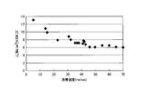
- the higher the vapor deposition rate the larger the film thickness formed during the same film formation time.
- the critical current value obtained per unit film formation time increases almost in proportion to the increase in the vapor deposition rate, so that it is possible to achieve both the increase in the critical current value and the improvement in productivity.
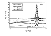
- FIG. 4 shows an example of the magnetic field angle dependence (relationship with the direction of the magnetic field) of the critical current value obtained per unit film formation time.
- the critical current value was measured under the conditions of a temperature of 30K and a magnetic field of 7T.
- the angle (deg.) on the horizontal axis is 0° when the angle of the magnetic field is perpendicular to the substrate, and 90° when the angle of the magnetic field is parallel to the substrate.
- a peak with an increased critical current value is seen near an angle of 90°, and in a region where the deposition rate is low, a peak due to a linear artificial pin rod is seen near an angle of 0°.
- the critical current value tends to be low as a whole.
- the anisotropy decreases in the range of ⁇ 45° to +45°, and the flat magnetic field angle dependence It turned out to show sex.
- introducing an artificial pin into the superconducting layer has the effect of increasing the critical current value in a magnetic field.
- the magnetic field dependence of the macroscopic pin force density of the superconducting layer changes with temperature.
- the phenomenon that the magnetic field dependence of the macroscopic pin force density changes with temperature may be suppressed by adjusting the vapor deposition rate of the superconducting layer as in the present invention.
- the cross section parallel to the thickness direction of the superconducting layers 1 to 6 was observed with a TEM (transmission electron microscope) to measure the tilt angle and the length of the artificial pin appearing in the superconducting layer in the region of 140 nm ⁇ 170 nm. ..
- the tilt angle is the tilt angle of the artificial pin with respect to the thickness direction of the superconducting layer.
- the length is the length of the artificial pin along the cross section. When the length direction of the artificial pin is not along the cross section, such as when the length is less than or equal to the thickness, it was excluded from the measurement targets of the inclination angle and the length.
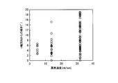
- FIG. 8 shows an example of the relationship between the vapor deposition rate and the inclination angle of the artificial pin (inclination from the c-axis direction).
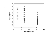
- FIG. 9 shows an example of the relationship between the deposition rate and the length of the artificial pin (rod length).
- Table 2 shows the minimum value, the maximum value, the average value, and the standard deviation of the inclination angle of the artificial pin measured for each sample.
- Table 3 shows the minimum value, the maximum value, the average value and the standard deviation of the lengths of the artificial pins.
- FIG. 10 shows an example of the relationship between the number density of artificial pins and the critical current density.
- the number density of artificial pins is determined by counting the number of artificial pins within a predetermined range from a plane TEM image in a plane (ab plane perpendicular to the c-axis) perpendicular to the thickness direction of the superconducting layer, and determining the area corresponding to the range. It was calculated by dividing.
- FIG. 10 was created by measuring the number density of artificial pins of a sample on which a superconducting layer was formed at a vapor deposition rate of about 40 nm/sec, and the critical current density at a temperature of 30K and a magnetic field of 2T.
- critical current density Jc was high when the number density was in the range of 1 ⁇ 10 3 to 3.5 ⁇ 10 3 pieces/ ⁇ m 2 .
- a preferable critical current density Jc is 6.0 MA/cm 2 or more at a temperature of 30K and a magnetic field of 2T.
- the number of artificial pins was 14 nm/sec at the deposition rate. It was found that when the density was increased to about 5 ⁇ 10 3 particles/ ⁇ m 2 , a-axis oriented grains were likely to occur. When the deposition rate is 40 nm/sec, the number density of artificial pins is 1 ⁇ 10 3 / ⁇ m 2 , 2 ⁇ 10 3 / ⁇ m 2 , 3 ⁇ 10 3 / ⁇ m 2 , 5 ⁇ 10 3 / ⁇ m 2 .
- a-axis oriented grains were not seen.
- the ratio of a-axis oriented grains can be calculated by the X-ray intensity ratio. As described above, in order to suppress the decrease in the critical current value, it is preferable that a-axis oriented grains are not observed.
Landscapes
- Chemical & Material Sciences (AREA)
- Organic Chemistry (AREA)
- Engineering & Computer Science (AREA)
- Materials Engineering (AREA)
- Manufacturing & Machinery (AREA)
- Inorganic Chemistry (AREA)
- Ceramic Engineering (AREA)
- Chemical Kinetics & Catalysis (AREA)
- Mechanical Engineering (AREA)
- Metallurgy (AREA)
- Structural Engineering (AREA)
- Toxicology (AREA)
- Health & Medical Sciences (AREA)
- Physics & Mathematics (AREA)
- Optics & Photonics (AREA)
- Superconductors And Manufacturing Methods Therefor (AREA)
- Inorganic Compounds Of Heavy Metals (AREA)
Abstract
基板に超電導層が積層された酸化物超電導線材であって、超電導層が、RE-Ba-Cu-O系酸化物超電導体と、ABO3を含む人工ピンとを有し、REは希土類元素、AはBa、Sr又はCa、BはHf、Zr又はSnを表し、超電導層の断面TEM像において、超電導層の厚さ方向に対する人工ピンの傾斜角の標準偏差σが、6.13~11.73°の範囲であり、人工ピンの長さの平均が、19.84~25.44nmの範囲である。
Description
本発明は、酸化物超電導線材及びその製造方法に関する。
本願は、2018年12月28日に、日本に出願された特願2018-248245号に基づき優先権を主張し、これらの内容をここに援用する。
本願は、2018年12月28日に、日本に出願された特願2018-248245号に基づき優先権を主張し、これらの内容をここに援用する。
REBa2Cu3Ox(REは希土類元素)等のRE-Ba-Cu-O系酸化物超電導体を用いた超電導線材の構造として、金属テープなどの基板上に中間層を介し、酸化物超電導層を成膜した構造が採用されている。特に近年では、磁場中の臨界電流値を向上させるために超電導層中に人工ピン材料を導入することが行われている(特許文献1及び非特許文献1参照)。
Tomo Yoshida, et al., "Yttrium-based Coated Conductors With Artifitial Pinning Centers", Fujikura Technical Review, No.47 November, 2017, pp.19-25
超電導線材の磁場中における臨界電流値を増加させる方法として、超電導層に人工ピンを添加する方法がある。超電導層に人工ピンを添加する方法の場合は、人工ピンをロッド状に成長させることで人工ピンがピンニングセンターとなり、磁場中の超電導特性を高めることができる。一方、生産性向上のために単位時間あたりに堆積される膜厚を厚くしようとして蒸着速度を大きくすると、超電導体の結晶性が乱れて、臨界電流値が低下する場合がある。
本発明は、上記事情に鑑みてなされたものであり、人工ピンが導入された超電導層を有する酸化物超電導線材において、臨界電流値の増加と蒸着速度を大きくすることにより生産性の向上を両立させることが可能な酸化物超電導線材及びその製造方法を提供する。
本発明の第1態様は、基板に超電導層が積層された酸化物超電導線材であって、前記超電導層が、RE-Ba-Cu-O系酸化物超電導体(REは希土類元素)と、ABO3(AはBa、Sr又はCaを表し、BはHf、Zr又はSnを表す。)を含む人工ピンを有し、前記超電導層の断面TEM像において、前記超電導層の厚さ方向に対する前記人工ピンの傾斜角の標準偏差σが、6.13~11.73°の範囲であり、前記人工ピンの長さの平均が、19.84~25.44nmの範囲である。
本発明の第2態様は、上記第1態様の酸化物超電導線材において、前記超電導層の厚さ方向に垂直な面内における前記人工ピンの数密度が1000~3500個/μm2であってもよい。
本発明の第3態様は、上記第1又は第2態様の酸化物超電導線材において、X線強度比によって算出される前記RE-Ba-Cu-O系酸化物超電導体のa軸配向粒の割合が10%以下であってもよい。
本発明の第4態様は、上記第1~第3態様の酸化物超電導線材において、温度30K、磁場2Tにおける臨界電流密度Jcが6.0MA/cm2以上であってもよい。
本発明の第3態様は、上記第1又は第2態様の酸化物超電導線材において、X線強度比によって算出される前記RE-Ba-Cu-O系酸化物超電導体のa軸配向粒の割合が10%以下であってもよい。
本発明の第4態様は、上記第1~第3態様の酸化物超電導線材において、温度30K、磁場2Tにおける臨界電流密度Jcが6.0MA/cm2以上であってもよい。
本発明の第5態様は、基板に超電導層が積層された、温度30K、c軸方向の磁場2Tにおける臨界電流密度Jcが6.0MA/cm2以上である酸化物超電導線材の製造方法であって、RE-Ba-Cu-O系酸化物超電導体(REは希土類元素)と、ABO3(AはBa、Sr又はCaを表し、BはHf、Zr又はSnを表す)を含む人工ピンとを有する前記超電導層を、パルスレーザ蒸着法(PLD法)で成膜する工程を備え、前記超電導層の蒸着速度が23nm/sec以上である。
本発明の第6態様は、上記第5態様の酸化物超電導線材の製造方法において、前記超電導層の蒸着速度が、36nm/sec以上であってもよい。
本発明の第7態様は、上記第6態様の酸化物超電導線材の製造方法において、前記超電導層の蒸着速度が、36~70nm/secであってもよい。
本発明の第8態様は、上記第7態様の酸化物超電導線材の製造方法において、前記超電導層の蒸着速度が、46~70nm/secであってもよい。
本発明の第9態様は、上記第5~第8態様のいずれか一態様の酸化物超電導線材の製造方法において、前記超電導層の厚さ方向に垂直な面内における前記人工ピンの数密度が1000~3500個/μm2であってもよい。
本発明の第7態様は、上記第6態様の酸化物超電導線材の製造方法において、前記超電導層の蒸着速度が、36~70nm/secであってもよい。
本発明の第8態様は、上記第7態様の酸化物超電導線材の製造方法において、前記超電導層の蒸着速度が、46~70nm/secであってもよい。
本発明の第9態様は、上記第5~第8態様のいずれか一態様の酸化物超電導線材の製造方法において、前記超電導層の厚さ方向に垂直な面内における前記人工ピンの数密度が1000~3500個/μm2であってもよい。
上記本発明の態様によれば、人工ピンを含有するため、臨界電流値の増加と生産性の向上を両立させることが可能になる。
以下、好適な実施形態に基づき、図面を参照して本発明を説明する。
図1に本実施形態の酸化物超電導線材を示す。本実施形態の酸化物超電導線材は、基板11に超電導層13が積層された酸化物超電導線材10である。基板11の表面には、超電導層13との間に中間層12を有することが好ましい。基板11、中間層12、超電導層13の各層が積層される方向が厚さ方向である。幅方向は、長手方向及び厚さ方向に垂直な方向である。
基板11は、テープ状の基板(基材)であり、厚さ方向の両側に、それぞれ主面(表面及びこれに対向する裏面)を有する。基板11を構成する金属の具体例として、ハステロイ(登録商標)に代表されるニッケル合金、ステンレス鋼、ニッケル合金に集合組織を導入した配向Ni-W合金などが挙げられる。基板11の厚さは、必要に応じて適宜調整すれば良く、例えば10~500μmの範囲である。基板11の裏面、側面、またはその両方には、接合性を改善するため、Ag、Cu等の金属薄膜をスパッタ等により形成してもよい。
超電導層13は、例えば一般式REBa2Cu3Oxで表されるRE-Ba-Cu-O系の酸化物超電導体が挙げられる。希土類元素REとしては、Sc、Y、La、Ce、Pr、Nd、Pm、Sm、Eu、Gd、Tb、Dy、Ho、Er、Tm、Yb、Luのうちの1種又は2種以上が挙げられる。超電導層13の厚さは、例えば0.5~5μm程度である。超電導層13を積層する方法としては、スパッタ法、真空蒸着法、レーザ蒸着法、電子ビーム蒸着法、パルスレーザ堆積法(PLD法)、化学気相成長法(CVD法)、有機金属塗布熱分解法(MOD法)等が挙げられる。中でも、生産性等の観点から、PLD法で超電導層13を積層することが好ましい。
超電導層13は、ABO3(AはBa、Sr又はCaを表し、BはHf、Zr又はSnを表す。)からなる人工ピンを含む。人工ピンを構成する材料(人工ピン材料)の具体例としては、BaHfO3、SrHfO3、CaHfO3、BaZrO3、BaSnO3等の少なくとも1種、これらの固溶体、又は2種以上の混合物等が挙げられる。人工ピンは、太さより長さが大きいロッド状であることが好ましい。人工ピンの長さとしては、平均が15~30nmの範囲内であることが好ましい。人工ピンの長さの平均の具体例として、19.84~25.44nmの範囲が挙げられる。人工ピンの太さとしては、平均が3~5nmであることが好ましく、平均が4~5nmであるとより好ましい。気相法で、基板11に垂直な方向に人工ピンを含む超電導体を堆積させる場合、超電導層は、基板面に垂直なc軸を有する傾向がある。この場合、人工ピンロッドは、超電導体のc軸方向あるいはそれから若干傾斜した方向に成長する傾向がある。
人工ピンロッドの成長する方向(ロッドの長手方向)がc軸方向に揃う場合、磁場がc軸方向に印加された場合は、特に強いピンニング力を示すが、それ以外の角度ではピンニングにあまり寄与しないという、異方性の問題がある。このため、人工ピンの長手方向は、超電導体のc軸から傾斜していることが好ましい。人工ピンの長手方向が超電導体のc軸から傾斜している場合、超電導体のa軸又はb軸に対する角度はランダムになり得るため、長手方向の異なる人工ピンが様々な角度の磁場に対するピンニングセンターとして寄与し、異方性の問題が改善される。例えば、超電導層13の厚さ方向に対する人工ピンの傾斜角(傾き)の標準偏差σが、5~20°の範囲内であることが好ましい。傾斜角の標準偏差σの具体例として、6.13~11.73°の範囲が挙げられる。
超電導層13の厚さ方向に垂直な面内における人工ピンの数密度は、1000~3500個/μm2の範囲内であることが好ましい。人工ピンの数密度が低いと、人工ピンの効果が低下する場合がある。
X線強度比によって算出されるRE-Ba-Cu-O系酸化物超電導体のa軸配向粒の割合が所定の範囲内であることが好ましい。具体的には、a軸配向粒の割合は、10%以下であることが好ましい。ここで、a軸配向粒の割合は、θ-2θ法によるX線回折測定で観測される(006)ピークと(200)ピークのピーク強度比〔(200)ピーク強度/(006)ピーク強度〕×100(%)で算出される値である。a軸配向粒の割合が少ないことにより、異常配向粒による超電導体の結晶性及び臨界電流の低下を抑制することができる。
本実施形態の酸化物超電導線材は、温度30K、磁場2Tにおける臨界電流密度Jcが6.0MA/cm2以上であることが好ましい。これにより、高い臨界電流を得ることができる。
本実施形態の酸化物超電導線材を製造する方法は、上述の酸化物超電導体及び人工ピンを含む超電導層を、パルスレーザ蒸着法(PLD法)で成膜する工程を有することが好ましい。酸化物超電導体及び人工ピンを含む超電導層を成膜する方法としては、超電導材料及び人工ピン材料を含有する混合ターゲットを用いる方法、超電導材料を含有する第1ターゲットと人工ピン材料を含有する第2ターゲットとの2種を用いる方法が挙げられる。超電導材料及び人工ピン材料を含有するターゲットを2種以上用いてもよい。超電導材料を含有する第1ターゲットは、超電導材料より低濃度の人工ピン材料を含有してもよく、あるいは実質的に人工ピン材料を含有しなくてもよい。人工ピン材料を含有する第2ターゲットは、人工ピン材料より低濃度の超電導材料を含有してもよく、あるいは実質的に超電導材料を含有しなくてもよい。組成が異なるターゲットを2種類以上用いる場合は、各ターゲットを並べて一体化してもよく、超電導層を成膜する空間(成膜空間)内で各ターゲットを異なる位置に配置してもよい。ターゲットにおける超電導材料に対する人工ピンの濃度としては、例えば、0.5~10mol%が挙げられる。ターゲットにおける人工ピン材料の濃度は、超電導層に対する人工ピンの濃度(モル濃度、数濃度)に応じて調整することができる。超電導層13は、ターゲットの超電導材料に由来するRE2O3等の不純物を含んでもよい。
本実施形態の製造方法では、人工ピンを含有する超電導層13の蒸着速度を速くすることが好ましい。超電導層13の蒸着速度としては、例えば、23nm/sec以上、さらには36nm/sec以上が好ましい。さらに、36~70nm/sec、特には46~70nm/secであることがより好ましい。蒸着速度を速くすることにより、人工ピンロッドが成膜方向(c軸方向)に沿って直線的に成長することを抑制し、c軸方向から傾斜を持った方向に人工ピンロッドが成長しやすくなる。このため、臨界電流の磁場角度依存性が低減される。また、成膜空間の温度変動を受けにくくなるため、人工ピン材料を超電導材料に添加しても、a軸配向粒の成長が抑制され、c軸配向膜を優先的に成長させることができる。また、超電導層13の蒸着速度を速くすることにより、生産性を向上することができる。
超電導層13の配向制御の観点からは、金属を含む基板11の表面に中間層12を設け、中間層12上に超電導層13を成膜することが好ましい。中間層12は、多層構成でもよく、例えば基板11側から超電導層13側に向かう順で、拡散防止層、ベッド層、配向層、キャップ層等を有してもよい。これらの層は必ずしも1層ずつ設けられるとは限らず、一部の層を省略する場合や、同種の層を2以上繰り返し積層する場合もある。
拡散防止層は、基板11の成分の一部が拡散し、不純物として超電導層13側に混入することを抑制する機能を有する。拡散防止層の材質としては、例えば、Si3N4、Al2O3、GZO(Gd2Zr2O7)等が挙げられる。拡散防止層の厚さは、例えば10~400nmである。
ベッド層は、基板11と超電導層13との界面における反応を低減し、ベッド層の上に形成される層の配向性を向上するために用いられる。ベッド層の材質としては、例えばY2O3、Er2O3、CeO2、Dy2O3、Eu2O3、Ho2O3、La2O3等が挙げられる。ベッド層の厚さは、例えば10~100nmである。
配向層は、その上のキャップ層の結晶配向性を制御するために2軸配向する物質から形成される。配向層の材質としては、例えば、Gd2Zr2O7、MgO、ZrO2-Y2O3(YSZ)、SrTiO3、CeO2、Y2O3、Al2O3、Gd2O3、Zr2O3、Ho2O3、Nd2O3等の金属酸化物を例示することができる。この配向層はIBAD(Ion-Beam-Assisted Deposition)法で形成することが好ましい。
キャップ層は、上述の配向層の表面に成膜されて、結晶粒が面内方向に自己配向し得る材料を有する。キャップ層の材質としては、例えば、CeO2、Y2O3、Al2O3、Gd2O3、ZrO2、YSZ、Ho2O3、Nd2O3、LaMnO3等が挙げられる。キャップ層の厚さは、50~5000nmの範囲が挙げられる。
超電導層13の表面には、保護層を設けることが好ましい。保護層は、事故時に発生する過電流をバイパスしたり、超電導層13と保護層の上に設けられる層との間で起こる化学反応を抑制したりする等の機能を有する。保護層の材質としては、例えば銀(Ag)、銅(Cu)、金(Au)、金と銀との合金、その他の銀合金、銅合金、金合金などが挙げられる。保護層は、少なくとも超電導層13の表面(厚さ方向で、基板11側に対する反対側の面)を覆っている。さらに保護層は、超電導層13の側面、中間層12の側面、基板11の側面、基板11の裏面から選択される領域の一部または全部を覆ってもよい。
超電導線材10は、基板11と超電導層13を含む積層体の周囲に、安定化層を有してもよい。安定化層を形成する領域としては、例えば基板11の裏面、超電導層13の表面、基板11又は超電導層13の側面が挙げられる。超電導線材10が保護層を有する場合は、保護層上に安定化層を設けてもよい。安定化層に用いられる材料は、超電導線材10の用途により異なってもよい。例えば、超電導ケーブルや超電導モータなどに使用する場合は、常電導状態への転移時に発生する過電流を転流させるバイパスのメイン部として機能する必要があるため、良導電性の金属が好適に用いられる。良導電性の金属として、銅、銅合金、アルミニウム、アルミニウム合金等の金属が挙げられる。また、超電導限流器に使用する場合は、常電導状態への転移時に発生する過電流を瞬時に抑制する必要があるため、高抵抗金属が好適に用いられる。高抵抗金属として、例えば、Ni-Cr等のNi系合金などが挙げられる。
以上、本発明を好適な実施形態に基づいて説明してきたが、本発明は上述の実施形態に限定されるものではなく、本発明の要旨を逸脱しない範囲で種々の改変が可能である。
超電導線材10は、テープ状、ケーブル状、コイル状等、種々の形態で使用することができる。超電導線材10を用いて超電導コイルを作製するには、超電導線材10を巻き枠の外周面に沿って必要な層数巻き付けてコイル形状(多層巻きコイル)とした後、巻き付けた超電導線材10を覆うようにエポキシ樹脂等の樹脂を含浸させて超電導線材10を固定することができる。また、超電導線材10は、外部端子を有することができる。外部端子を有する箇所では、他の箇所と異なる断面構造を有してもよい。
以下、実施例をもって本発明を具体的に説明する。
ハステロイ(登録商標)を有するテープ状の基板にイオンビームスパッタ法等を用いて中間層を形成した。人工ピン材料としてBaHfO3を添加したEuBa2Cu3Oxターゲットを使用し、PLD法により超電導層を形成して、超電導線材を作製した。ターゲットにおけるBaHfO3の添加量と蒸着速度を変更して各々の超電導線材を試作した。
蒸着速度は、例えば、PLD装置のレーザのパルス周波数[Hz]やPLD成膜時の雰囲気圧力[Pa]を調整することで適宜設定可能である。
レーザのパルス周波数は、例えば10~1000Hzの範囲で調整され得る。レーザのパルス周波数を増大させると、人工ピンの傾斜角度の標準偏差が増大し、人工ピンの長さの平均値は減少する傾向をもつ。
PLD成膜は、成膜チャンバ内に酸素ガスを流入させた状態で行う。具体的には、真空ポンプを用いて成膜チャンバを減圧したあと酸素ガスを流入させ、酸素ガスの流入量を調整することで雰囲気圧力を一定に維持しつつPLD成膜を行う。成膜時の雰囲気圧力は、例えば1~1000Paの範囲で調整され得る。PLD成膜時の雰囲気圧力を増大させることで、人工ピンの傾斜角度の標準偏差が増大し、人工ピンの長さの平均値は減少する傾向をもつ。
蒸着速度は、例えば、PLD装置のレーザのパルス周波数[Hz]やPLD成膜時の雰囲気圧力[Pa]を調整することで適宜設定可能である。
レーザのパルス周波数は、例えば10~1000Hzの範囲で調整され得る。レーザのパルス周波数を増大させると、人工ピンの傾斜角度の標準偏差が増大し、人工ピンの長さの平均値は減少する傾向をもつ。
PLD成膜は、成膜チャンバ内に酸素ガスを流入させた状態で行う。具体的には、真空ポンプを用いて成膜チャンバを減圧したあと酸素ガスを流入させ、酸素ガスの流入量を調整することで雰囲気圧力を一定に維持しつつPLD成膜を行う。成膜時の雰囲気圧力は、例えば1~1000Paの範囲で調整され得る。PLD成膜時の雰囲気圧力を増大させることで、人工ピンの傾斜角度の標準偏差が増大し、人工ピンの長さの平均値は減少する傾向をもつ。
試作した超電導線材について、四端子法でc軸方向の磁場中における臨界電流値を測定した。臨界電流値の測定条件は、温度30K、磁場2Tとした。超電導線材の臨界電流値と超電導層の断面積とから、超電導層の温度30K、磁場2Tにおける臨界電流密度Jcを算出した。図2に、超電導層の蒸着速度と臨界電流密度Jcの関係の一例を示す。蒸着速度が小さい23nm/sec未満の領域では、蒸着速度の増加に伴い、臨界電流密度が単調に減少する傾向がみられた。蒸着速度が23nm/sec以上(詳細には、23~70nm/sec、36~70nm/sec、または46~70nm/sec)の範囲では、蒸着速度を増加するように変化させても、臨界電流密度の値が、好適な臨界電流密度の目安となる6.0MA/cm2以上を維持しつつ、ほぼ一定の値をとっていることが分かった。
具体的には、蒸着速度が23nm/sec未満の領域では、蒸着速度が大きくなるに従い臨界電流密度の値が急峻に低下することが分かった。この領域では、超電導層に導入される人工ピンロッドがc軸方向に沿って成長し、形状も揃った状態となり易く、ピン止め効果によって臨界電流密度が高くなると考えられる。しかし、蒸着速度が遅いため生産性が低い。蒸着速度が23~70nm/secの範囲では、超電導層に導入される人工ピンロッドの向きや形状が乱れ過ぎずに適度に揃った状態であると考えられ、6.0MA/cm2以上の臨界電流密度を維持しつつ、高い生産性を実現することができた。なお、本実施例においては、使用したPLD装置の仕様により蒸着速度が70nm/secより大きな領域で超電導線材を試作し評価することができなかったが、蒸着速度が大き過ぎると、超電導層に導入される人工ピンロッドの向きや形状が揃わず過剰に乱れた状態となると考えられ、臨界電流密度も次第に低くなると予想される。
図2及び後述の表1に示された超電導層の蒸着速度と臨界電流密度Jcとの関係から、蒸着速度が23nm/sec以上、さらには、23~70nm/secの範囲では、臨界電流密度Jcは6.0MA/cm2以上となり、臨界電流密度Jcと生産性とを高いレベルで両立できる。蒸着速度が36nm/sec以上、さらには、36~70nm/secの範囲では、蒸着速度が大きくかつ臨界電流密度Jcは6.0MA/cm2以上となり、臨界電流密度Jcと生産性とを高いレベルで両立できる。さらに、蒸着速度が46~70nm/secの範囲では、蒸着速度がより大きくかつ臨界電流密度Jcは6.0MA/cm2以上となり、臨界電流密度Jcと生産性とをより高いレベルで両立できる。
図3に、蒸着速度と臨界電流Icとの関係の一例を示す。図3の縦軸は、臨界電流密度Jcと蒸着速度の積をとること等により、単位成膜時間(sec)当たり、かつ単位幅(cm-w)当たりに得られる臨界電流を示す。蒸着速度が高いほど、同じ成膜時間で成膜される膜厚が増加する。図3に示すように、単位成膜時間当たりに得られる臨界電流値は、蒸着速度の増加にほぼ比例して増加することから、臨界電流値の増加と生産性の向上を両立させることが可能となる。特に蒸着速度31~50nm/secの範囲で、蒸着速度を変化させても、臨界電流値は256.1~322.4A/sec/cm-wの範囲でほぼ一定の値をとっていることが分かった。また、蒸着速度41~50nm/secの範囲で、蒸着速度を変化させても、臨界電流値は280.5~322.4A/sec/cm-wの範囲でほぼ一定の値をとっていることが分かった。蒸着速度が55nm/secを超えると、蒸着速度が大きくなるに従い臨界電流値の値も大きくなった。
表1に、図2及び図3のグラフに対応する臨界電流密度Jc及び臨界電流Icの値を示す。
表1に、図2及び図3のグラフに対応する臨界電流密度Jc及び臨界電流Icの値を示す。

図4に、単位成膜時間当たりに得られる臨界電流値の磁場角度依存性(磁場の方向との関係)の一例を示す。臨界電流値は、温度30K、磁場7Tの条件で測定した。横軸の角度(deg.)は、磁場の角度が基板に垂直な場合に0°、磁場の角度が基板に平行な場合に90°となる。いずれの試料にも角度90°付近に臨界電流値が高まるピークがみられるほか、蒸着速度が低い領域では、直線状の人工ピンロッドに起因したピークが角度0°付近にみられる。しかし、蒸着速度が低いと、全体的には臨界電流値が低い傾向を示している。これに対して、蒸着速度が高い領域では、全体的に高い臨界電流値を示すことに加え、-45°から+45°の範囲で異方性が減少して、平坦(フラット)な磁場角度依存性を示すことが分かった。
臨界電流の磁場角度依存性の違いを考察するため、各々の蒸着速度で成膜した超電導層のサンプルについてTEM(透過型電子顕微鏡)を用いた断面観察を行い、一例を図5(蒸着速度5nm/sec)、図6(蒸着速度14nm/sec)、図7(蒸着速度32nm/sec)に示す。これらの断面TEM画像は、超電導層の厚さ方向に平行な断面を撮影した像である。断面組織観察で確認される人工ピンロッドは、蒸着速度が低いと超電導体の結晶c軸方向に沿って直線状に成長する傾向を示していた。これに対して、蒸着速度が高いと人工ピンロッドの成長方向が結晶c軸方向から傾き、ランダムな向きに成長する傾向を示していた。このことが、フラットな磁場角度依存性に寄与していることが分かる。
一般的に、超電導層に人工ピンを導入することによって、磁場中における臨界電流値を増大するという効果が得られる。しかし他方では、超電導層の巨視的ピン力密度の磁場依存性が温度によって変化してしまう現象が知られている。この巨視的ピン力密度の磁場依存性が温度によって変化する現象は、本発明のように超電導層の蒸着速度を調整することによって抑制できる可能性がある。
サンプルNo.1~6の超電導層の厚さ方向に平行な断面をTEM(透過型電子顕微鏡)で観察して、140nm×170nmの領域の超電導層中に出現した人工ピンの傾斜角及び長さを測定した。傾斜角は、超電導層の厚さ方向に対する人工ピンの傾斜角である。長さは、断面に沿った人工ピンの長さである。長さが太さ以下である場合等、人工ピンの長さ方向が断面に沿っていない場合は、傾斜角及び長さの測定対象から除外した。図8に、蒸着速度と人工ピンの傾斜角(c軸方向からの傾き)との関係の一例を示す。図9に、蒸着速度と人工ピンの長さ(ロッド長さ)との関係の一例を示す。これらのグラフでは、蒸着速度が32nm/secと同じサンプル3~6の結果は、まとめて示した。表2に、各サンプルについて測定した人工ピンの傾斜角の最小値、最大値、平均値及び標準偏差を示す。表3には、人工ピンの長さの最小値、最大値、平均値及び標準偏差を示す。
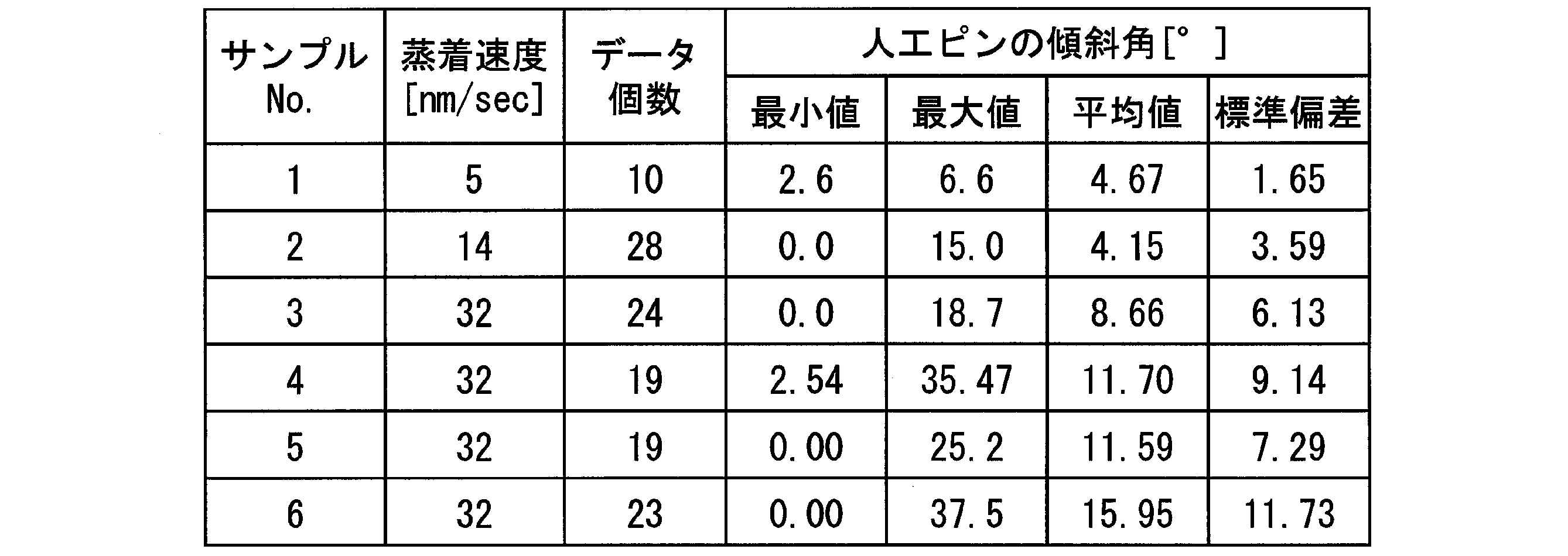
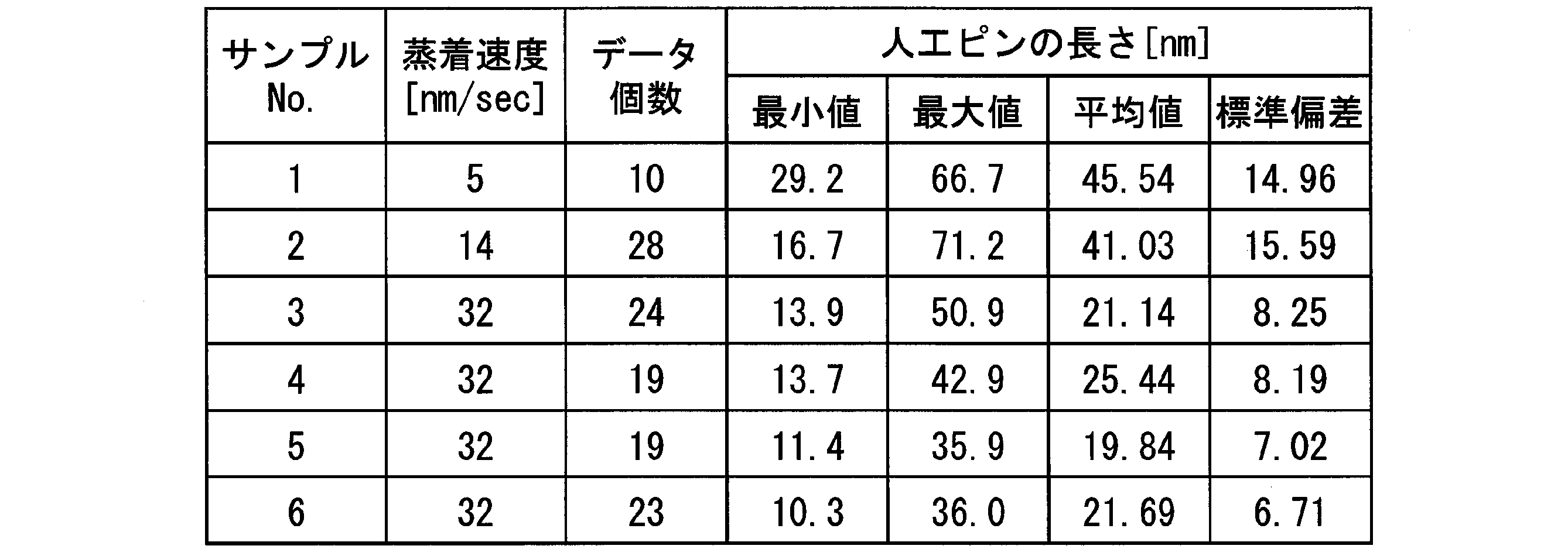
図10に、人工ピンの数密度と臨界電流密度の関係の一例を示す。人工ピンの数密度は、超電導層の厚さ方向に垂直な面(c軸に垂直なab面)内における平面TEM画像から所定の範囲内で人工ピンの数を数え、範囲に相当する面積を除して算出した。図10は、蒸着速度が約40nm/secで超電導層を成膜したサンプルの人工ピンの数密度と、温度30K、磁場2Tにおける臨界電流密度を測定して作成した。数密度が1×103~3.5×103個/μm2の範囲であれば臨界電流密度Jcが高いことが分かった。好ましい臨界電流密度Jcとしては、温度30K、磁場2Tにおいて6.0MA/cm2以上が挙げられる。
また、蒸着速度14nm/sec又は40nm/secで成膜した超電導層の表面の平面TEM画像を、一辺が20~30nm程度の範囲に撮影したところ、蒸着速度が14nm/secでは、人工ピンの数密度が5×103個/μm2程度まで増加した場合、a軸配向粒が生じやすいことが分かった。蒸着速度が40nm/secでは、人工ピンの数密度が1×103個/μm2、2×103個/μm2、3×103個/μm2、5×103個/μm2のいずれにおいても、a軸配向粒がみられなかった。なお、a軸配向粒の割合は、X線強度比によって算出することができる。上述したように、臨界電流値の低下を抑制するには、a軸配向粒がみられない状態が好ましい。
10…酸化物超電導線材、11…基板、12…中間層、13…超電導層
Claims (9)
- 基板に超電導層が積層された酸化物超電導線材であって、
前記超電導層が、RE-Ba-Cu-O系酸化物超電導体と、ABO3を含む人工ピンとを有し、REは希土類元素、AはBa、Sr又はCa、BはHf、Zr又はSnを表し、
前記超電導層の断面TEM像において、前記超電導層の厚さ方向に対する前記人工ピンの傾斜角の標準偏差σが、6.13~11.73°の範囲であり、前記人工ピンの長さの平均が、19.84~25.44nmの範囲である、
酸化物超電導線材。 - 前記超電導層の厚さ方向に垂直な面内における前記人工ピンの数密度が1000~3500個/μm2である、請求項1に記載の酸化物超電導線材。
- X線強度比によって算出される前記RE-Ba-Cu-O系酸化物超電導体のa軸配向粒の割合が10%以下である、請求項1又は2に記載の酸化物超電導線材。
- 温度30K、磁場2Tにおける臨界電流密度Jcが6.0MA/cm2以上である、請求項1~3のいずれか1項に記載の酸化物超電導線材。
- 基板に超電導層が積層された、温度30K、c軸方向の磁場2Tにおける臨界電流密度Jcが6.0MA/cm2以上である酸化物超電導線材の製造方法であって、
RE-Ba-Cu-O系酸化物超電導体(REは希土類元素)と、ABO3(AはBa、Sr又はCaを表し、BはHf、Zr又はSnを表す)を含む人工ピンとを有する前記超電導層を、パルスレーザ蒸着法(PLD法)で成膜する工程を備え、
前記超電導層の蒸着速度が23nm/sec以上である、
酸化物超電導線材の製造方法。 - 前記超電導層の蒸着速度が、36nm/sec以上である、請求項5に記載の酸化物超電導線材の製造方法。
- 前記超電導層の蒸着速度が、36~70nm/secである、請求項6に記載の酸化物超電導線材の製造方法。
- 超電導層の蒸着速度が、46~70nm/secである、請求項7に記載の酸化物超電導線材の製造方法。
- 前記超電導層の厚さ方向に垂直な面内における前記人工ピンの数密度が1000~3500個/μm2である、請求項5~8のいずれか1項に記載の酸化物超電導線材の製造方法。
Priority Applications (5)
| Application Number | Priority Date | Filing Date | Title |
|---|---|---|---|
| EP19902603.0A EP3904292A4 (en) | 2018-12-28 | 2019-12-09 | OXIDE SUPERCONDUCTING WIRE AND METHOD OF PRODUCTION THEREOF |
| JP2020539102A JP6788152B1 (ja) | 2018-12-28 | 2019-12-09 | 酸化物超電導線材及びその製造方法 |
| US17/268,334 US11267722B2 (en) | 2018-12-28 | 2019-12-09 | Oxide superconducting wire and method of manufacturing the same |
| RU2021103698A RU2753187C1 (ru) | 2018-12-28 | 2019-12-09 | Сверхпроводящий оксидный провод и способ его изготовления |
| CN201980049207.9A CN112469668A (zh) | 2018-12-28 | 2019-12-09 | 氧化物超导线材及其制造方法 |
Applications Claiming Priority (2)
| Application Number | Priority Date | Filing Date | Title |
|---|---|---|---|
| JP2018248245 | 2018-12-28 | ||
| JP2018-248245 | 2018-12-28 |
Publications (1)
| Publication Number | Publication Date |
|---|---|
| WO2020137490A1 true WO2020137490A1 (ja) | 2020-07-02 |
Family
ID=71125850
Family Applications (1)
| Application Number | Title | Priority Date | Filing Date |
|---|---|---|---|
| PCT/JP2019/048094 Ceased WO2020137490A1 (ja) | 2018-12-28 | 2019-12-09 | 酸化物超電導線材及びその製造方法 |
Country Status (6)
| Country | Link |
|---|---|
| US (1) | US11267722B2 (ja) |
| EP (1) | EP3904292A4 (ja) |
| JP (1) | JP6788152B1 (ja) |
| CN (1) | CN112469668A (ja) |
| RU (1) | RU2753187C1 (ja) |
| WO (1) | WO2020137490A1 (ja) |
Cited By (1)
| Publication number | Priority date | Publication date | Assignee | Title |
|---|---|---|---|---|
| WO2022064912A1 (ja) * | 2020-09-25 | 2022-03-31 | 株式会社フジクラ | 酸化物超電導線材 |
Families Citing this family (2)
| Publication number | Priority date | Publication date | Assignee | Title |
|---|---|---|---|---|
| RU2761855C1 (ru) * | 2021-07-21 | 2021-12-13 | Общество с ограниченной ответственностью "С-Инновации" | Гибкий высокотемпературный сверхпроводник и способ его получения |
| CN121148812B (zh) * | 2025-11-17 | 2026-04-28 | 甚磁科技(上海)有限公司 | 一种临界电流密度非均匀分布的高温超导带材及其制备方法 |
Citations (2)
| Publication number | Priority date | Publication date | Assignee | Title |
|---|---|---|---|---|
| JPS5736522B2 (ja) | 1978-06-02 | 1982-08-04 | ||
| WO2017217487A1 (ja) * | 2016-06-16 | 2017-12-21 | 株式会社フジクラ | 酸化物超電導線材及びその製造方法 |
Family Cites Families (7)
| Publication number | Priority date | Publication date | Assignee | Title |
|---|---|---|---|---|
| JP2005056754A (ja) * | 2003-08-06 | 2005-03-03 | Sumitomo Electric Ind Ltd | 超電導線材およびその製造方法 |
| US8034745B2 (en) * | 2005-08-01 | 2011-10-11 | Amit Goyal | High performance devices enabled by epitaxial, preferentially oriented, nanodots and/or nanorods |
| ES2302637B1 (es) * | 2006-12-14 | 2009-06-05 | Consejo Superior Investig. Cientificas | Material superconductor nanoestructurado tipo reba2cu3o7(re=tierra rara o ytrio) con una elevada densidad de centros de anclaje de vortices y su metodo de preparacion. |
| EP2728589A4 (en) * | 2011-06-30 | 2015-04-15 | Int Superconductivity Tech | SUPRENEES OF THE RE-123 WIRE AND METHOD FOR THE PRODUCTION THEREOF |
| WO2013109065A1 (en) * | 2012-01-17 | 2013-07-25 | Sunam Co., Ltd. | Superconducting wire and method of forming the same |
| WO2014103995A1 (ja) * | 2012-12-28 | 2014-07-03 | 公益財団法人国際超電導産業技術研究センター | Re123系超電導線材およびその製造方法 |
| JP6374365B2 (ja) * | 2015-09-16 | 2018-08-15 | 株式会社東芝 | 酸化物超電導体、およびその製造方法 |
-
2019
- 2019-12-09 WO PCT/JP2019/048094 patent/WO2020137490A1/ja not_active Ceased
- 2019-12-09 US US17/268,334 patent/US11267722B2/en active Active
- 2019-12-09 JP JP2020539102A patent/JP6788152B1/ja active Active
- 2019-12-09 CN CN201980049207.9A patent/CN112469668A/zh active Pending
- 2019-12-09 EP EP19902603.0A patent/EP3904292A4/en not_active Withdrawn
- 2019-12-09 RU RU2021103698A patent/RU2753187C1/ru active
Patent Citations (2)
| Publication number | Priority date | Publication date | Assignee | Title |
|---|---|---|---|---|
| JPS5736522B2 (ja) | 1978-06-02 | 1982-08-04 | ||
| WO2017217487A1 (ja) * | 2016-06-16 | 2017-12-21 | 株式会社フジクラ | 酸化物超電導線材及びその製造方法 |
Non-Patent Citations (4)
| Title |
|---|
| ICHINOSE ATARU, TSURUTA AKIHIRO, MIURA SHUN, ICHINO YUSUKE, YOSHIDA YUTAKA: "Improvement of Jc Properties through Control of Nanorod Morphology", TEION KŌGAKU, vol. 48, no. 9, 25 September 2013 (2013-09-25), pages 485 - 492, XP009525635, DOI: 10.2221/jcsj.48.485 * |
| See also references of EP3904292A4 |
| TOMO YOSHIDA ET AL.: "Yttrium-based Coated Conductors With Artificial Pinning Centers", FUJIKURA TECHNICAL REVIEW, no. 47, November 2017 (2017-11-01), pages 19 - 25, XP055775838 |
| YOSHIDA, TOMO ET AL.: "Yttrium-based Coated Conductors with Artificial Pinning Centers", FUJIKURA TECHNICAL REVIEW, June 2017 (2017-06-01), pages 19 - 25, XP055775838 * |
Cited By (5)
| Publication number | Priority date | Publication date | Assignee | Title |
|---|---|---|---|---|
| WO2022064912A1 (ja) * | 2020-09-25 | 2022-03-31 | 株式会社フジクラ | 酸化物超電導線材 |
| JP2022053796A (ja) * | 2020-09-25 | 2022-04-06 | 株式会社フジクラ | 酸化物超電導線材 |
| CN116194408A (zh) * | 2020-09-25 | 2023-05-30 | 株式会社藤仓 | 氧化物超导电线材 |
| EP4219401A4 (en) * | 2020-09-25 | 2024-10-16 | Fujikura Ltd. | OXIDE-BASED SUPERCONDUCTING WIRE |
| US12573527B2 (en) | 2020-09-25 | 2026-03-10 | Fujikura Ltd. | Oxide superconducting wire |
Also Published As
| Publication number | Publication date |
|---|---|
| US11267722B2 (en) | 2022-03-08 |
| JP6788152B1 (ja) | 2020-11-18 |
| EP3904292A4 (en) | 2022-09-21 |
| US20210323834A1 (en) | 2021-10-21 |
| EP3904292A1 (en) | 2021-11-03 |
| CN112469668A (zh) | 2021-03-09 |
| RU2753187C1 (ru) | 2021-08-12 |
| JPWO2020137490A1 (ja) | 2021-02-18 |
Similar Documents
| Publication | Publication Date | Title |
|---|---|---|
| RU2414769C2 (ru) | Сверхпроводящий провод | |
| JP6788152B1 (ja) | 酸化物超電導線材及びその製造方法 | |
| US20140148343A1 (en) | Re123-based superconducting wire and method of manufacturing the same | |
| US20140349854A1 (en) | Iron-based superconducting material, iron-based superconducting layer, iron-based superconducting tape wire material, and iron-based superconducting wire material | |
| JP6743233B1 (ja) | 酸化物超電導線材 | |
| JP5799081B2 (ja) | 単層コーティングによる酸化物厚膜 | |
| US8772201B2 (en) | Oxide superconducting conductor and method of manufacturing the same | |
| EP3474296A1 (en) | Oxide superconducting wire and method for manufacturing same | |
| US20130231250A1 (en) | Oxide superconducting conductor and method of manufacturing the same | |
| US8216977B2 (en) | High temperature superconductors | |
| EP1990810A1 (en) | Process for producing superconducting thin-film material, superconducting equipment and superconducting thin-film material | |
| JP5736522B2 (ja) | Re123系超電導線材およびその製造方法 | |
| WO2013015328A1 (ja) | 超電導薄膜用基材、超電導薄膜及び超電導薄膜の製造方法 | |
| KR101612149B1 (ko) | 전구체의 제조 방법, 초전도 선재의 제조 방법, 전구체 및 초전도 선재 | |
| JP2020135988A (ja) | 酸化物超電導線材及びその製造方法 | |
| JP7449763B2 (ja) | 酸化物超電導線材および酸化物超電導線材の製造方法 | |
| JP2011249162A (ja) | 超電導線材の製造方法 | |
| JP2012204190A (ja) | 酸化物超電導薄膜 | |
| JP2023121990A (ja) | 酸化物超電導積層体、酸化物超電導線材および接続構造体 | |
| JP2026000612A (ja) | 超伝導デバイス及び超伝導デバイスの製造方法 | |
| JP2016143516A (ja) | 酸化物超電導線材及びその製造方法 | |
| JP6404556B2 (ja) | 酸化物超電導導体およびその製造方法 | |
| WO2020195996A1 (ja) | 酸化物超電導線材 |
Legal Events
| Date | Code | Title | Description |
|---|---|---|---|
| ENP | Entry into the national phase |
Ref document number: 2020539102 Country of ref document: JP Kind code of ref document: A |
|
| 121 | Ep: the epo has been informed by wipo that ep was designated in this application |
Ref document number: 19902603 Country of ref document: EP Kind code of ref document: A1 |
|
| NENP | Non-entry into the national phase |
Ref country code: DE |
|
| ENP | Entry into the national phase |
Ref document number: 2019902603 Country of ref document: EP Effective date: 20210728 |