WO2020149053A1 - 光学装置、画像表示装置及び表示装置 - Google Patents
光学装置、画像表示装置及び表示装置 Download PDFInfo
- Publication number
- WO2020149053A1 WO2020149053A1 PCT/JP2019/048256 JP2019048256W WO2020149053A1 WO 2020149053 A1 WO2020149053 A1 WO 2020149053A1 JP 2019048256 W JP2019048256 W JP 2019048256W WO 2020149053 A1 WO2020149053 A1 WO 2020149053A1
- Authority
- WO
- WIPO (PCT)
- Prior art keywords
- light
- guide plate
- light guide
- deflecting member
- deflection
- Prior art date
- Legal status (The legal status is an assumption and is not a legal conclusion. Google has not performed a legal analysis and makes no representation as to the accuracy of the status listed.)
- Ceased
Links
Images











Classifications
-
- G—PHYSICS
- G02—OPTICS
- G02B—OPTICAL ELEMENTS, SYSTEMS OR APPARATUS
- G02B27/00—Optical systems or apparatus not provided for by any of the groups G02B1/00 - G02B26/00, G02B30/00
- G02B27/01—Head-up displays
- G02B27/017—Head mounted
- G02B27/0172—Head mounted characterised by optical features
-
- G—PHYSICS
- G02—OPTICS
- G02B—OPTICAL ELEMENTS, SYSTEMS OR APPARATUS
- G02B27/00—Optical systems or apparatus not provided for by any of the groups G02B1/00 - G02B26/00, G02B30/00
- G02B27/0081—Optical systems or apparatus not provided for by any of the groups G02B1/00 - G02B26/00, G02B30/00 with means for altering, e.g. enlarging, the entrance or exit pupil
-
- G—PHYSICS
- G02—OPTICS
- G02B—OPTICAL ELEMENTS, SYSTEMS OR APPARATUS
- G02B6/00—Light guides; Structural details of arrangements comprising light guides and other optical elements, e.g. couplings
- G02B6/0001—Light guides; Structural details of arrangements comprising light guides and other optical elements, e.g. couplings specially adapted for lighting devices or systems
- G02B6/0011—Light guides; Structural details of arrangements comprising light guides and other optical elements, e.g. couplings specially adapted for lighting devices or systems the light guides being planar or of plate-like form
- G02B6/0075—Arrangements of multiple light guides
- G02B6/0076—Stacked arrangements of multiple light guides of the same or different cross-sectional area
-
- G—PHYSICS
- G02—OPTICS
- G02B—OPTICAL ELEMENTS, SYSTEMS OR APPARATUS
- G02B27/00—Optical systems or apparatus not provided for by any of the groups G02B1/00 - G02B26/00, G02B30/00
- G02B27/01—Head-up displays
- G02B27/0101—Head-up displays characterised by optical features
- G02B2027/0123—Head-up displays characterised by optical features comprising devices increasing the field of view
- G02B2027/0125—Field-of-view increase by wavefront division
-
- G—PHYSICS
- G02—OPTICS
- G02B—OPTICAL ELEMENTS, SYSTEMS OR APPARATUS
- G02B27/00—Optical systems or apparatus not provided for by any of the groups G02B1/00 - G02B26/00, G02B30/00
- G02B27/01—Head-up displays
- G02B27/017—Head mounted
- G02B27/0172—Head mounted characterised by optical features
- G02B2027/0174—Head mounted characterised by optical features holographic
-
- G—PHYSICS
- G02—OPTICS
- G02B—OPTICAL ELEMENTS, SYSTEMS OR APPARATUS
- G02B27/00—Optical systems or apparatus not provided for by any of the groups G02B1/00 - G02B26/00, G02B30/00
- G02B27/01—Head-up displays
- G02B27/017—Head mounted
- G02B2027/0178—Eyeglass type
-
- G—PHYSICS
- G02—OPTICS
- G02B—OPTICAL ELEMENTS, SYSTEMS OR APPARATUS
- G02B5/00—Optical elements other than lenses
- G02B5/18—Diffraction gratings
- G02B5/1814—Diffraction gratings structurally combined with one or more further optical elements, e.g. lenses, mirrors, prisms or other diffraction gratings
- G02B5/1819—Plural gratings positioned on the same surface, e.g. array of gratings
-
- G—PHYSICS
- G02—OPTICS
- G02B—OPTICAL ELEMENTS, SYSTEMS OR APPARATUS
- G02B5/00—Optical elements other than lenses
- G02B5/18—Diffraction gratings
- G02B5/1842—Gratings for image generation
Definitions
- the present disclosure relates to an optical device, an image display device including such an optical device, and a display device including such an image display device, and more specifically to a head mounted display (HMD, Head Mounted Display).
- the present invention relates to a display device used.
- HMD head-mounted display
- various types of head-mounted displays have been studied, there is a strong demand for a wider angle of view of the display image in order to provide a more realistic image to the head-mounted display. ..
- a head-mounted display in which three deflecting means are arranged on a light guide plate that constitutes an optical device is disclosed in, for example, US Patent Publication 2006/0132914A1 or US Patent Publication 2014/0330966A1. It is well known.
- Japanese Patent Laid-Open No. 2009-133998 discloses that (A) An image forming apparatus having a plurality of pixels arranged in a two-dimensional matrix, (B) A collimating optical system that collimates light emitted from the pixels of the image forming apparatus, and (C) An optical device in which a plurality of parallel lights having different traveling directions are incident, guided, and emitted in the collimating optical system, An image display device comprising: The optical device is (A) A light guide plate that is emitted after the incident light propagates through the inside by total internal reflection, (B) A reflection type volume hologram diffraction grating that diffracts and reflects the light incident on the light guide plate so that the light incident on the light guide plate is totally reflected inside the light guide plate.
- a first diffraction grating member and (C) A second diffraction grating member provided on the light guide plate, which is a reflection type volume hologram diffraction grating that diffracts and reflects the light propagated by total reflection inside the light guide plate and emits the light from the light guide plate.
- a center line of the first diffraction grating member is an origin, and a normal line of the first diffraction grating member passing through the origin and having a positive direction in a direction toward the collimating optical system side passes through the X i axis and the origin, and
- the axis of the light guide plate orthogonal to the i- axis and having the direction toward the second diffraction grating member side as the positive direction is the Y i- axis
- the central light emitted from the pixel at the center of the image forming apparatus and passing through the center of the collimating optical system is optically parallel to the X i Y i plane and has an acute angle with respect to the X i Z i plane.
- the head-mounted display disclosed in the above two US patent publications it is not possible to meet the demand for a wider angle of view of the displayed image.
- the image display device disclosed in Japanese Patent Application Laid-Open No. 2009-133998 has only two diffraction grating members, that is, the first diffraction grating member and the second diffraction grating member, the first diffraction grating and the second diffraction grating member are used.
- the display image area can be enlarged in the light guide plate only in one direction propagating to the grating.
- an object of the present disclosure is to provide an optical device having a configuration and structure capable of further widening the angle of view of a display image, an image display device including the optical device, and a display including the image display device. To provide a device.
- the optical device of the present disclosure for achieving the above object, An optical device in which light emitted from an image forming apparatus is incident, guided, and emitted, A first light guide plate and a second light guide plate; and a first deflection unit provided on the first light guide plate and a second deflection unit provided on the second light guide plate.
- the first deflection unit includes a first A deflection member, a first B deflection member and a first C deflection member
- the second deflection unit is composed of a second A deflection member, a second B deflection member and a second C deflection member, Part of the light emitted from the image forming apparatus is incident on the first A deflection member, The light incident on the first A deflecting member is deflected by the first A deflecting member, is totally reflected inside the first light guide plate, enters the first B deflecting member, is deflected by the first B deflecting member, and is reflected by the first light guide plate.
- the light is totally reflected inside and enters the first C deflecting member, is deflected by the first C deflecting member, and is emitted toward the observer's pupil. At least the remaining part of the light emitted from the image forming apparatus is incident on the second A deflection member, The light incident on the second A deflecting member is deflected by the second A deflecting member, is totally reflected inside the second light guide plate, is incident on the second B deflecting member, is deflected by the second B deflecting member, and is reflected by the second light guide plate. The light is totally reflected inside and is incident on the second C deflecting member, is deflected by the second C deflecting member, and is emitted toward the observer's pupil.
- Propagation direction of the light deflected by the first B-deflecting member in the first light guide plate is the first direction when the projection direction is orthogonal to the first light guide plate, and propagation of light deflected by the second B-deflecting member in the second light guide plate.
- the direction when the direction is orthographically projected onto the first light guide plate is the second direction
- the first direction is the opposite direction to the second direction.
- the image display device of the present disclosure for achieving the above object, An image forming apparatus, and An optical device in which light emitted from the image forming apparatus is incident, guided, and emitted, An image display device comprising:
- the optical device comprises the optical device of the present disclosure.
- the display device of the present disclosure for achieving the above object is A frame attached to the observer's head, and Image display device attached to the frame, A display device comprising:
- the image display device includes an image forming device, and an optical device into which light emitted from the image forming device is incident, guided, and emitted.
- the optical device comprises the optical device of the present disclosure.
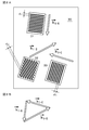
- FIGS. 1A and 1B are schematic diagrams of the first light guide plate and the first deflection unit, and the second light guide plate and the second deflection unit that configure the optical device of the first embodiment.
- 2A and 2B are schematic views of the arrangement of the first A deflecting member, the first B deflecting member, and the first C deflecting member, and the first A deflecting member, the first B deflecting member, and It is a conceptual diagram of a wave number vector and the like of the first C deflecting member.
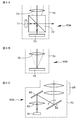
- 3A and 3B are schematic cross-sectional views of the optical device of Example 1
- FIG. 3C is a schematic view of the optical device as viewed from the side.
- FIG. 4 is a schematic view of the optical device of Example 1 viewed from above.
- FIG. 5 is a schematic view of the display device of Example 1 viewed from the front.
- 6A, 6B, and 6C are conceptual diagrams of the image forming apparatus in the display device of the first embodiment.
- FIG. 7 is a conceptual diagram showing the arrangement of the image forming apparatus, the light guide plate, the first A deflection member, the second A deflection member, and the like in the optical device of the first embodiment.
- FIG. 8A and FIG. 8B are schematic diagrams showing the arrangement and the first stage of the first light guide plate and the first deflection unit, and the second light guide plate and the second deflection unit that configure the optical device of the first embodiment.
- 11A and 11B are schematic diagrams of the arrangement and the second stage of the arrangement of the first A deflection member, the first B deflection member, and the first C deflection member constituting the optical device of the first embodiment, and the arrangement and the second stage, respectively. It is a conceptual diagram of a wave number vector etc. of a 1A deflection member, a 1B deflection member, and a 1C deflection member.
- 12A and 12B are schematic diagrams illustrating the arrangement and second stage of the first light guide plate and the first deflection unit that configure the optical device of the first embodiment.
- FIG. 13 is a schematic diagram of the first light guide plate and the first deflection unit that configure the optical device of the second embodiment.
- FIG. 14 is a schematic diagram of the second light guide plate and the second deflection unit that configure the optical device of the second embodiment.
- 15A, 15B, 15C, 15D, 15E, 15F, 15G, and 15H are conceptual diagrams of modified examples of the optical device of the first embodiment.
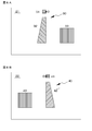
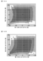
- 16A and 16B are diagrams showing the results of simulating the image area obtained in the optical device of the first embodiment.
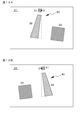
- FIG. 17 is a diagram showing a result of simulating an image area obtained in the optical device of the first embodiment.
- 18A and 18B are diagrams showing results of simulating the propagation states of light in the first light guide plate and the second light guide plate obtained in the optical device of the first embodiment, respectively.
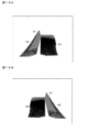
- FIGS. 16A, 16B and 17 are diagrams showing results of simulating images obtained by the first deflection unit and the second deflection unit obtained in the optical device of the first embodiment, respectively.
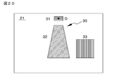
- FIG. 20 is a schematic diagram showing an arrangement state of the first A deflecting member, the first B deflecting member and the first C deflecting member forming the first deflecting unit for obtaining the result of the simulation shown in FIGS. 16A, 16B and 17. Is.
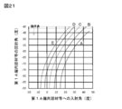
- FIG. 21 is a graph showing the relationship between the incident angle of light on the first A deflecting member or the second A deflecting member and the diffraction angle of the first A deflecting member or the second A deflecting member with the pitch d as a parameter.
- 22A, 22B and 22C are diagrams for explaining the XYZ Cartesian coordinate system and the (x 0 , y 0 , z 0 ) Cartesian coordinate system.
- optical device of the present disclosure optical device configuring the image display device of the present disclosure, optical device configuring the display device of the present disclosure (hereinafter, these may be collectively referred to as “optical device of the present disclosure”)
- the first light guide plate and the second light guide plate can be arranged side by side. That is, the first light guide plate and the second light guide plate can be arranged in parallel with each other with an air layer in between, for example.
- An origin is a point on the first light guide plate where a light beam emitted from the center point of the image forming area of the image forming apparatus collides with the first light guide plate
- the bisector of an acute intersection angle is The axis containing the bisector going toward is the +X axis
- the Z axis is the axis that passes through the origin and is perpendicular to the first light guide plate.
- the first direction which is the direction when the propagation direction of the light deflected by the first B deflecting member in the first light guide plate is orthographically projected onto the first light guide plate, is the +X axis direction, but is not parallel to the +X axis.
- the second direction which is a direction when the propagation direction of the light that is extended in parallel and is deflected by the second B deflection member in the second light guide plate is orthographically projected onto the first light guide plate, is the ⁇ X axis direction, It extends non-parallel to or parallel to the X-axis. That is, the first direction and the second direction are non-parallel or collinear.
- the first A deflecting member and the second A deflecting member may be arranged symmetrically on the YZ plane and may be symmetrical and have the same shape, or may be different shapes.
- the first B deflecting member and the second B deflecting member may be arranged symmetrically with respect to the YZ plane and may be symmetrical and have the same shape, or may have different shapes.
- the first C deflecting member and the second C deflecting member may be arranged symmetrically with respect to the YZ plane and may be symmetrical and have the same shape, or may have different shapes. it can.
- the first deflection unit is arranged in a state of being rotated about a Z axis in a counterclockwise or clockwise first rotation direction
- the second deflection unit may be arranged so as to be rotated about the Z axis in the second rotation direction of the clockwise direction or the counterclockwise direction.
- the second deflection unit may be placed in a state of being rotated in the second rotation direction, and instead of arranging the second deflection unit in a state of being rotated in the second rotation direction, the second A deflection member, the second B deflection member, and the second C deflection member of the second deflection unit are arranged.
- the wave vector may be rotated in the second rotation direction.
- the angle formed by the direction of light incident on the first B deflection member and the direction of light emitted from the first B deflection member is ⁇ 1
- 90 degrees ⁇ 1 90 degrees ⁇ 2 It can be a form that satisfies 90 degrees ⁇ 1 ⁇ 105 degrees 90 degrees ⁇ 2 ⁇ 105 degrees
- 99.5 (degrees) ⁇ ⁇ 1 ⁇ 2 ⁇ 100.5 (degrees) It is preferable to satisfy
- the second B-deflecting member orthographic image when orthographically projected onto one light guide plate may be partially overlapped (in some cases, in contact), and further, the first B-deflecting member normal image may be formed.
- the second B-deflecting member orthographic image may be in contact with the ⁇ X-axis direction end).
- the first B deflection member orthographic image when the first B deflection member is orthographically projected onto the first light guide plate and the second B deflection member orthographic image when the second B deflection member is orthographically projected onto the first light guide plate.
- the first C-deflecting member orthogonal projection image and the +X-axis direction end portion of the second C-deflecting member orthogonal projection image are in contact with each other. Form).
- first A deflection member orthographic image when the first A deflection member is orthographically projected onto the first light guide plate and the second A deflection member orthographic image when the second A deflection member is orthographically projected onto the first light guide plate. It is possible to have a form in which they partially overlap (in some cases, they are in contact with each other), and further, the +X-axis direction end portion of the first A deflection member orthogonal projection image and the second A deflection member orthogonal projection image.
- the first A deflection member and the second A deflection member are composed of a volume hologram diffraction grating
- the wave vector of the first A deflection member is k v 1-A
- the X component, Y component, and Z component of k v 1-A are k X 1-A , k Y 1-A , and k Z 1-A
- the wave number vector of the second A deflection member is k v 2-A
- the X component, Y component, and Z component of k v 2-A are k X 2-A , k Y 2-A , and k Z 2-A .
- the first C deflecting member and the second C deflecting member are composed of a volume hologram diffraction grating
- the wave number vector of the first C deflection member is k v 1-C
- the X component, Y component, and Z component of k v 1-C are k X 1-C , k Y 1-C , and k Z 1-C
- the wave number vector of the second C deflection member is k v 2-C
- the X component, Y component, and Z component of k v 2-C are k X 2-C , k Y 2-C , and k Z 2-C .
- the first B deflecting member and the second B deflecting member are composed of a volume hologram diffraction grating
- the wave vector of the first B-deflecting member is k v 1-B
- the X component, Y component, and Z component of k v 1-B are k X 1-B , k Y 1-B , and k Z 1-B
- the wave number vector of the second B-deflecting member is k v 2-B
- the X, Y, and Z components of k v 2-B are k X 2-B , k Y 2-B , and k Z 2-B .
- the volume hologram diffraction grating is of a transmission type. It may be a reflective type.
- the volume hologram diffraction grating means a hologram diffraction grating that diffracts only +1st order diffracted light.
- the first A deflecting member, the first B deflecting member and the first C deflecting member are composed of a volume hologram diffraction grating,
- the average diffraction efficiency of the first A deflection member with respect to the light emitted from the image forming apparatus is ⁇ 1-A
- the average diffraction efficiency of the first B deflection member is ⁇ 1-B
- the average diffraction efficiency of the first C deflection member is ⁇ 1-C.
- the second A deflecting member, the second B deflecting member and the second C deflecting member are composed of a volume hologram diffraction grating
- the average diffraction efficiency of the second A deflection member with respect to the light emitted from the image forming apparatus is ⁇ 2-A
- the average diffraction efficiency of the second B deflection member is ⁇ 2-B
- the average diffraction efficiency of the second C deflection member is ⁇ 2-C.
- ⁇ 2-B / ⁇ 2-A ⁇ 1 ⁇ 2-C / ⁇ 2-A ⁇ 1 Can be satisfied.
- the diffraction efficiency ⁇ is I 1 /when the light intensity of the light incident on the volume hologram diffraction grating is I 0 and the light intensity of the + 1st order diffracted light diffracted by the volume hologram diffraction grating is I 1 . It is represented by I 0 .
- the diffraction efficiency can be controlled by, for example, the thickness of the volume hologram diffraction grating. That is, the smaller the thickness of the volume hologram diffraction grating, the lower the value of the diffraction efficiency ⁇ .
- the light quantity of the light emitted from the area of the hologram diffraction grating is LI 1
- the light quantity of the light emitted from the area of the next closest volume hologram diffraction grating is LI 2
- the light quantity of the light emitted from the area of the third closest volume hologram diffraction grating is LI 4
- first A deflecting member and the second A deflecting member are collectively referred to as “first A deflecting member and the like”, and the first B deflecting member and the second B deflecting member are collectively referred to as “first 1B deflecting member etc.”, and the 1C deflecting member and the 2C deflecting member may be collectively referred to as "1C deflecting member etc.”
- the light beam emitted from the center point of the image forming area of the image forming apparatus is vertically incident on the first A deflecting member and the second A deflecting member.
- the light may be incident at a certain angle that is not vertical.
- An origin is a point on the first light guide plate where a light beam emitted from the center point of the image forming area of the image forming apparatus collides with the first light guide plate
- the bisector of an acute intersection angle is The axis containing the bisector going toward is the +X axis
- the Z axis is the axis that passes through the origin and is perpendicular to the first light guide plate.
- the angle formed by the orthogonal projection image and the X-axis when the ray emitted from the center point of the image forming area of the image forming apparatus and incident on the origin is orthogonally projected onto the first light guide plate (XZ plane) is less than 90 degrees. Is preferable, and more preferably 70 degrees or more and less than 90 degrees. Further, the angle formed by the orthogonal projection image and the Y-axis when the ray emitted from the center point of the image forming area of the image forming apparatus and incident on the origin is orthogonally projected to the YZ plane is ⁇ 20 degrees or more and 20 degrees or less. Is desirable.
- the material forming the first light guide plate and the second light guide plate has a refractive index of 1.5 or more, preferably 1.6 or more.
- the material forming the volume hologram diffraction grating may have a refractive index of 1.5 or more, preferably 1.6 or more.
- the optical device is a semi-transmissive type (see-through type). Specifically, at least the portion of the optical device facing the eyeball (pupil) of the observer is made semi-transmissive (see-through), and this portion of the optical device (specifically, at least the first C deflection member and the second C deflection member) is used. You can see the outside through.
- semi-transmissive does not mean that half (50%) of incident light is transmitted or reflected, but a part of incident light is transmitted and the rest is reflected. It is used to mean that
- the image display device or the display device of the present disclosure can display a single color (for example, green) image.
- the first A deflecting member, the first B deflecting member, etc. and the first C which are composed of one diffraction grating layer. It is also possible to adopt a configuration in which P types of interference fringes are formed on the deflecting member or the like.
- the first first light guide plate and the second light guide plate are composed of a diffraction grating layer formed of a volume hologram diffraction grating that diffracts/reflects light having a red wavelength band (or wavelength).
- a first A deflecting member, etc., a first B deflecting member, etc., and a first C deflecting member, etc., which are composed of a diffraction grating layer composed of a volume hologram diffraction grating are arranged, and a third first light guide plate and second light guide plate, blue The first A deflection member, etc., the first B deflection member, etc.
- the first C deflection member, etc. which are composed of a diffraction grating layer composed of a volume hologram diffraction grating for diffracting light having a wavelength band (or wavelength) of A structure in which six light guide plates are stacked with a gap therebetween may be adopted.
- a first A deflecting member or the like, a first B deflecting member or the like and a first C deflecting member or the like for diffracting light having the above are diffracted, and light having a blue or red wavelength band is diffracted on the other surface of the first light guide plate.
- the 1A deflection member, etc., the 1B deflection member, etc. and the 1C deflection member, etc. may be arranged.
- one surface of the second light guide plate has a green wavelength band together with a second A deflection member etc., a second B deflection member etc. and a second C deflection member etc. for diffracting light having a red or blue wavelength band.
- Second A for diffracting light having a wavelength band of blue or red is laminated on the other surface of the second light guide plate by laminating a second A deflecting member etc. for diffracting light, a second B deflecting member etc. and a second C deflecting member etc.
- the deflecting member and the like, the second B deflecting member and the like, and the second C deflecting member and the like may be arranged.
- the diffraction efficiency is increased when light having each wavelength band (or wavelength) is diffracted by the first A deflecting member, etc., the first B deflecting member, etc. and the first C deflecting member, etc. It is possible to increase the diffraction acceptance angle and optimize the diffraction angle. It is preferable to dispose the protective member so that the volume hologram diffraction grating does not come into direct contact with the atmosphere.
- a photopolymer material can be mentioned as a material forming the volume hologram diffraction grating.
- the constituent material and the basic structure of the volume hologram diffraction grating in the optical device and the like of the present disclosure may be the same as the constituent material and the structure of the conventional volume hologram diffraction grating.
- interference fringes are formed from the inside to the surface, and the method of forming the interference fringes themselves may be the same as the conventional forming method.
- a material (eg, a photopolymer material) forming the volume hologram diffraction grating is irradiated with object light from a first predetermined direction on one side, and at the same time, the volume hologram diffraction grating is formed.
- the reference light is irradiated to the material to be used from the second predetermined direction on the other side, and interference fringes formed by the object light and the reference light may be recorded inside the material forming the volume hologram diffraction grating. ..
- the first predetermined direction, the second predetermined direction, the wavelengths of the object light and the reference light, the desired pitch of the interference fringes and the desired inclination angle of the interference fringes on the surface of the volume hologram diffraction grating. (Slant angle) can be obtained.
- the tilt angle of the interference fringe means the angle formed by the surface of the volume hologram diffraction grating and the interference fringe.
- a diffraction grating layer may be produced.
- the tilt angle (slant angle) of the interference fringes may be constant in the volume hologram diffraction grating, or may be changed depending on the value of the angle of view of the image incident on the volume hologram diffraction grating.
- the inclination angle of the interference fringes is changed depending on the value of the angle of view of the incident image, it may be changed continuously or stepwise.
- the diffraction efficiency of the interference fringes may be changed continuously or stepwise by changing the interference ratio between the object light and the reference light.
- the material forming the volume hologram diffraction grating (the photopolymer material forming the photosensitive material precursor layer before irradiation with the object light and the reference light) is composed of at least a photopolymerizable compound, a binder resin, and a photopolymerization initiator. Any photopolymer material, if configured, can be used.
- a photopolymerizable compound for example, a known photopolymerizable compound such as an acrylic monomer, a methacrylic monomer, a styrene monomer, a butadiene monomer, a vinyl monomer, or an epoxy monomer can be used. These may be copolymers and may be monofunctional or polyfunctional.
- binder resin may be used. Specifically, specifically, cellulose acetate resin, acrylic resin, acrylic ester resin, methacrylic acid resin, epoxy resin, urethane resin, polypropylene resin, polyvinyl ether. Resin, polycarbonate resin, polyamide resin, polyvinyl acetate, vinyl chloride resin, urea resin, styrene resin, butadiene resin, natural rubber resin, polyvinyl carbazole, polyethylene glycol, phenolic resin, or their copolymers Coalescence, gelatin, etc. can be mentioned.
- the binder resin may be used alone or in combination.
- the photopolymerization initiator any known one can be used.
- the photopolymerization initiator may be used alone, in a plurality, or in combination with a plurality or a single photosensitizing dye.
- a plasticizer, a chain transfer agent, and other additives may be appropriately added to the photosensitive material precursor layer.
- any material for forming the protective layer for protecting the volume hologram diffraction grating any material can be used as long as it is transparent, and even if it is formed by coating, a film-formed material is used as a photosensitive material precursor layer. It may be laminated to.
- Examples of the material forming the protective layer include polyvinyl alcohol (PVA) resin, acrylic resin, polyurethane resin, polyethylene terephthalate (PET) resin, triacetyl cellulose (TAC) resin, polymethylmethacrylate (PMMA) resin, polypropylene resin. , Polycarbonate resin, polyvinyl chloride resin.
- PVA polyvinyl alcohol
- PET polyethylene terephthalate
- TAC triacetyl cellulose
- PMMA polymethylmethacrylate
- Polypropylene resin polypropylene resin
- Polycarbonate resin polyvinyl chloride resin.
- the image forming device may have a form having a plurality of pixels arranged in a two-dimensional matrix. Note that the configuration of such an image forming apparatus will be referred to as a “first configuration image forming apparatus” for convenience.
- an image forming apparatus of the first configuration for example, an image forming apparatus including a reflective spatial light modulator and a light source; an image forming apparatus including a transmissive spatial light modulator and a light source; an organic EL (Electro Luminescence) element , An inorganic EL element, a light emitting diode (LED), an image forming apparatus including a light emitting element such as a semiconductor laser element.
- an image forming apparatus including a reflective spatial light modulator and a light source Alternatively, it is preferable that the image forming apparatus includes an organic EL element.
- the spatial light modulator examples include a light valve, for example, a transmissive or reflective liquid crystal display device such as LCOS (Liquid Crystal On Silicon), a digital micromirror device (DMD), and a light emitting element as a light source. be able to.
- the reflective spatial light modulator reflects a part of the light from the liquid crystal display device and the light source to the liquid crystal display device and passes a part of the light reflected by the liquid crystal display device. It can be configured to include a polarization beam splitter that guides the light to the optical system.
- Examples of the light emitting element that constitutes the light source include a red light emitting element, a green light emitting element, a blue light emitting element and a white light emitting element, or red light emitted from the red light emitting element, the green light emitting element and the blue light emitting element.
- white light may be obtained by mixing green light and blue light with a light pipe to uniformize the brightness.
- Examples of the light emitting element include a semiconductor laser element, a solid-state laser, and an LED.
- the number of pixels may be determined based on the specifications required for the image display device, and specific values of the number of pixels include 320 ⁇ 240, 432 ⁇ 240, 640 ⁇ 480, 1024 ⁇ 768, 1920 ⁇ 1080, etc. Can be illustrated.
- the image forming device includes a light source, and a scanning unit that scans the parallel light emitted from the light source. It can be in the form.
- the configuration of such an image forming apparatus will be referred to as a "second configuration image forming apparatus" for convenience.
- the light source in the image forming apparatus of the second structure may be a light emitting element, specifically, a red light emitting element, a green light emitting element, a blue light emitting element, a white light emitting element, or a red light emitting element.
- White light may be obtained by mixing the red light, the green light, and the blue light emitted from the device, the green light emitting device, and the blue light emitting device with a light pipe to uniformize the brightness.
- the light emitting element include a semiconductor laser element, a solid-state laser, and an LED.
- the number of pixels (virtual pixels) in the image forming apparatus having the second configuration may be determined based on the specifications required for the image display device, and 320 ⁇ is a specific value of the number of pixels (virtual pixels).
- 240, 432x240, 640x480, 1024x768, 1920x1080, etc. can be illustrated.
- the scanning means include MEMS (Micro Electro Mechanical Systems) and a galvano mirror that horizontally scan and vertically scan the light emitted from the light source and have a micromirror that is rotatable in a two-dimensional direction.
- an optical system an optical system that makes emitted light from the image forming apparatus parallel light, and may be referred to as “parallel light emitting optical system”, Specifically, for example, a plurality of light beams that are collimated by a collimating optical system or a relay optical system are made incident on the light guide plate. This is based on the fact that the light wavefront information when entering the light guide plate needs to be stored even after it is emitted from the light guide plate through the first A deflection member, the first B deflection member, etc. and the first C deflection member, etc.
- the light emitting unit of the image forming apparatus may be positioned at the position (position) of the focal length in the parallel light emitting optical system. ..
- the parallel light emitting optical system has a function of converting position information of pixels into angle information in the optical system of the optical device.
- Examples of the parallel light emitting optical system include an optical system having a positive optical power as a whole, which is a single or combination of a convex lens, a concave lens, a free-form surface prism, and a hologram lens.
- an appropriate light guide means is provided between the parallel light emitting optical system and the first A deflecting member and the second A deflecting member. It can be placed between them.
- a reflecting mirror can be used as the light guide means. Further, the light emitted from the parallel light emitting optical system may be directly focused on the first A deflection member and the second A deflection member.
- the light guide plate has two parallel surfaces (first surface and second surface).
- first surface and second surface When the surface of the light guide plate on which light enters is the light guide plate entrance surface and the surface of the light guide plate on which light exits is the light guide plate exit surface, even if the first surface configures the light guide plate entrance surface and the light guide plate exit surface.
- the first surface may form the light guide plate entrance surface
- the second surface may form the light guide plate exit surface.
- glass including quartz glass or optical glass such as BK7, or a plastic material for example, PMMA, polycarbonate resin, acrylic resin, amorphous polypropylene resin, styrene resin including AS resin)
- a plastic material for example, PMMA, polycarbonate resin, acrylic resin, amorphous polypropylene resin, styrene resin including AS resin
- the shape of the light guide plate is not limited to the flat plate and may have a curved shape.
- the material having a refractive index of 1.5 or more include BK7, a polycarbonate resin, an amorphous polypropylene resin, and a styrene resin including an AS resin.
- An acrylate resin can be exemplified.
- the image display device may be equipped with a light control device. That is, the optical device may overlap at least a portion of the dimmer. More specifically, it is preferable that at least the first C deflecting member and the second C deflecting member of the optical device overlap with the light control device.
- the dimmer will be described later in detail.
- the frame may include a front portion arranged in front of the observer and two temple portions rotatably attached to both ends of the front portion via hinges. it can. A modern part is attached to the tip of each temple part.
- the image display device is attached to the frame, specifically, for example, the image forming device may be attached to the upper portion of the front portion.
- the front part and the two temple parts may be integrated. That is, when the entire display device of the present disclosure is viewed, the frame has substantially the same structure as normal glasses.
- the material forming the frame including the pad portion can be made of the same material as the material forming normal eyeglasses, such as metal, alloy, plastic, or a combination thereof.
- the nose pad may be attached to the front portion. That is, when the entire display device of the present disclosure is viewed, the assembly of the frame (including the rim) and the nose pad has substantially the same structure as ordinary glasses.
- the nose pad can also have a known configuration and structure.
- the wiring (signal line, power supply line, etc.) from one or two image forming devices is provided in the temple portion, and from the viewpoint of design or ease of mounting. It is desirable that the modern portion extends to the outside from the tip portion of the modern portion via the inside of the modern portion and is connected to a control device (control circuit or control means). Furthermore, each image forming apparatus is provided with a headphone section, and the wiring for the headphone section from each image forming apparatus passes from the tip of the modern section to the headphone section through the temple section and the inside of the modern section. It can also be an extended form. Examples of the headphone unit include an inner ear type headphone unit and a canal type headphone unit.
- the headphone wiring extends from the tip portion of the modern portion to the headphone portion so as to wrap around the back side of the auricle (auricle).
- the image pickup device may be attached to the central portion of the front portion.
- the image pickup device includes a solid-state image pickup device including a CCD or CMOS sensor and a lens.
- the wiring from the imaging device may be connected to, for example, one image display device (or the image forming device) via the front portion, and is further included in the wiring extending from the image display device (or the image forming device). Good.
- the display device can configure, for example, a head-mounted display (HMD). This makes it possible to reduce the weight and size of the display device, significantly reduce discomfort when mounting the display device, and further reduce the manufacturing cost. ..
- the image display device of the present disclosure can be applied to a head-up display (HUD) provided in a cockpit of a vehicle or an aircraft.
- the virtual image forming area in which a virtual image is formed based on the light emitted from the image forming apparatus can be a HUD arranged on the windshield of the cockpit of a vehicle or an aircraft, or alternatively, the image forming can be performed.
- a combiner having a virtual image forming area in which a virtual image is formed based on light emitted from the device may be a HUD arranged on the windshield of a vehicle or aircraft cockpit.
- Example 1 relates to the optical device of the present disclosure, the image display device of the present disclosure, and the display device of the present disclosure.
- FIG. 1A shows a schematic view of the first light guide plate and the first deflection unit that configure the optical device of Example 1
- FIG. 1B shows a schematic view of the second light guide plate and the second deflection unit.
- FIG. 2A a schematic view of the arrangement of the first A deflecting member, the first B deflecting member and the first C deflecting member constituting the optical device of Example 1 is shown in FIG. 2A, and the 1A deflecting member, the 1B deflecting member and the 1C deflecting member are shown.
- FIG. 2B shows a conceptual diagram of the wave number vector of the above.
- FIGS. 3A and 3B schematic sectional views of the optical device of Example 1 are shown in FIGS. 3A and 3B, a schematic view of the optical device viewed from the side is shown in FIG. 3C, and a schematic view of the optical device of Example 1 viewed from above.
- FIG. 4 is shown
- FIG. 5 is a schematic view of the display device of the first embodiment viewed from the front
- conceptual diagrams of the image forming apparatus in the display device of the first embodiment are shown in FIGS. 6A, 6B, and 6C.
- .. 1A, FIG. 1B, FIG. 8A, FIG. 8B, FIG. 10A, FIG. 10B, FIG. 12A, and FIG. 12B are conceptual views of the optical device constituting the image display device for the right eye as viewed from the front.
- the observer's nose is located on the right hand side and the observer's ear is located on the left hand side of the figure.
- the optical device 10 is an optical device in which light emitted from the image forming apparatus 60 is incident, guided, and emitted.
- the first light guide plate 21 and the second light guide plate 22, and the first deflection unit 30 provided in the first light guide plate 21 and the second deflection unit 40 provided in the second light guide plate 22 are provided,
- the first deflection unit 30 includes a first A deflection member 31, a first B deflection member 32, and a first C deflection member 33,
- the second deflection unit 40 is composed of a second A deflection member 41, a second B deflection member 42 and a second C deflection member 43.
- the first A deflection member 31 a part of the light emitted from the image forming apparatus 60 is incident on the first A deflection member 31,
- the light that has entered the first A deflection member 31 is deflected by the first A deflection member 31, totally reflected inside the first light guide plate 21, enters the first B deflection member 32, and is deflected by the first B deflection member 32.
- the light is totally reflected inside the first light guide plate 21, enters the first C deflection member 33, is deflected by the first C deflection member 33, and is emitted toward the observer's pupil 90.
- the second A deflection member 41 At least the remaining part of the light emitted from the image forming apparatus 60 is incident on the second A deflection member 41,
- the light incident on the second A deflecting member 41 is deflected by the second A deflecting member 41, is totally reflected inside the second light guide plate 22, enters the second B deflecting member 42, and is deflected by the second B deflecting member 42.
- the light is totally reflected inside the second light guide plate 22, enters the second C deflection member 43, is deflected by the second C deflection member 43, and is emitted toward the observer's pupil 90.
- the direction of the light deflected by the first B-deflecting member 32 in the first light guide plate 21 is orthogonally projected to the first light guide plate 21, and the direction of the light deflected by the second B-deflecting member 42 is the first direction.
- the propagation direction of the second light guide plate 22 is orthogonally projected to the first light guide plate 21
- the first direction is opposite to the second direction.
- the first direction and the second direction are not parallel.
- the state is not limited to such a state, and in some cases, the first direction and the second direction may be on the same straight line.
- the image display device 11 of the first embodiment is The image forming apparatus 60, and An optical device in which light emitted from the image forming apparatus 60 is incident, guided, and emitted, Is equipped with The optical device comprises the optical device 10 of the first embodiment.
- the display device of Example 1 is A frame 50 mounted on the observer's head, and The image display device 11 attached to the frame 50, Is equipped with The image display device 11 includes an image forming device 60 and an optical device into which light emitted from the image forming device 60 is incident, guided, and emitted.
- the optical device comprises the optical device 10 of the first embodiment.
- the first light guide plate 21 and the second light guide plate 22 are arranged side by side. That is, the 1st light guide plate 21 and the 2nd light guide plate 22 are spaced apart and arranged in parallel, for example, via an air layer.
- the display device of the first embodiment is specifically a binocular type having two image display devices 11, but may be a single eye type having one.
- the optical device 10 is a see-through type (semi-transmissive type).
- the image forming apparatus 60 displays a monochrome image, but the invention is not limited to this.
- the image display apparatus for the right eye will be described below based on the coordinate axis of the right-handed system, but the image display apparatus for the left eye may be read as the coordinate axis of the left-handed system.
- a point on the first light guide plate 21 at which a light beam emitted from the center point of the image forming area of the image forming apparatus 60 collides with the first light guide plate 21 is defined as an origin O
- an origin O In the XYZ Cartesian coordinate system that passes through the origin O, Of the intersection angles at which a straight line passing through the origin O and parallel to the first direction and a straight line passing through the origin O and parallel to the second direction intersect, a bisector of an acute intersection angle,
- the +X axis is the axis that includes the bisector in the direction.
- An axis passing through the origin O and perpendicular to the first light guide plate 21 is a Z axis,
- the first deflection unit 30 and the second deflection unit 40 are arranged at positions symmetrical with respect to the YZ plane.
- the light beam emitted from the center point of the image forming area of the image forming apparatus 60 may be vertically incident on the first A deflection member 31 and the second A deflection member 41. As described above, a mode in which the light is incident at an angle may be adopted. Further, it is assumed that the light beam emitted from the center point of the image forming area of the image forming apparatus 60 is incident on the center of the observer's pupil.
- the first direction which is the direction when the propagation direction of the light deflected by the first B deflecting member 32 in the first light guide plate 21 is orthographically projected onto the first light guide plate 21, extends in the +X axis direction. However, it extends non-parallel to the +X axis.
- the second direction which is the direction when the propagation direction of the light deflected by the second B deflecting member 42 in the second light guide plate 22 is orthographically projected onto the first light guide plate 21, extends in the ⁇ X axis direction. However, it extends non-parallel to the -X axis.
- a (x 0 , y 0 , z 0 ) Cartesian coordinate system centered on the origin O is assumed.
- the x 0 axis is an axis parallel to the pupil center line passing through the center of the observer's pupil 90. It z 0 axis is in the XZ plane, y 0 axis orthogonal to the x 0 axis and y 0 axis.
- the “+” direction of the x 0 axis is the direction away from the observer.
- the “+” direction of the z 0 axis is the direction from the observer's ear to nose.
- the "pupillary axis" is defined as a line that passes through the center of the entrance pupil of the eye and is perpendicular to the corneal surface.
- the first light guide plate 21 and the second light guide plate 22 may be arranged so that the X axis coincides with the x 0 axis and the Z axis coincides with the z 0 axis. .. 22A, 22B, and 22C, the light beam emitted from the center point of the image forming area of the image forming apparatus 60 is indicated by a dotted line, and the pupil center line is indicated by a one-dot chain line.
- FIG. 3 is a diagram relating to the image display device of FIG.
- the end portion A of the first light guide plate 21 and the second light guide plate 22 located on the observer's nose side is more than the end portion B located on the observer's ear side.
- the angle ⁇ 0 formed by the X axis and the z 0 axis is a value exceeding 0 degrees ( ⁇ 0 >0).
- the value of ⁇ 0 is 0 (degree) ⁇ 0 ⁇ 20 (degree) It is preferable to satisfy Further, when the angle formed by the X axis and the Y axis when the light beam emitted from the center point of the image forming area of the image forming apparatus 60 enters the origin O is ( ⁇ X , ⁇ Y ), that is, image formation
- the angle formed by the orthogonal projection image and the X-axis when the light ray emitted from the center point of the image forming area of the apparatus and incident on the origin O is orthographically projected onto the first light guide plate 21 (XZ plane) is ⁇ X
- the image forming apparatus When the angle between the Y-axis and the orthogonal projection image when the ray emitted from the center point of the image forming area and incident on the origin O is orthographically projected on the YZ plane is ⁇ Y , the center of the image forming area of the image forming apparatus is When the light beam emitted from the point
- the angle ( ⁇ X formed by the orthogonal projection image and the X axis when the light beam emitted from the center point of the image forming area of the image forming apparatus and incident on the origin O is orthographically projected onto the first light guide plate 21 (XZ plane).
- the angle ( ⁇ Y ) formed by the orthogonal projection image and the Y axis when the light ray emitted from the center point of the image forming area of the image forming apparatus and incident on the origin O is orthographically projected on the YZ plane is ⁇ 20 degrees or more, It is preferably 20 degrees or less.
- the first A deflection member 31 and the second A deflection member 41 forming the first deflection unit 30 and the second deflection unit 40 are arranged symmetrically in the YZ plane, and are symmetrical and have the same shape. is there.
- the first B deflecting member 32 and the second B deflecting member 42 are arranged symmetrically in the YZ plane and are symmetrical and have the same shape
- the first C deflecting member 33 and the second C deflecting member 43 are the same.
- YZ planes are arranged symmetrically and are symmetrical and have the same shape.
- the first deflection unit 30 displays an image with a horizontal angle of view of 20 degrees to a horizontal angle of view of 0 degrees and a vertical angle of view of ⁇ 20 degrees
- the second deflection unit 40 has a horizontal angle of view of 0 degrees.
- an image having a horizontal field angle of ⁇ 20 degrees and a vertical field angle of ⁇ 20 degrees is displayed. That is, in the optical device of the first embodiment, specifically, half of the light emitted from the image forming apparatus 60 is incident on the first A deflecting member 31, and the image is incident on the second A deflecting member 41. The other half of the light emitted from the forming device 60 is incident.
- the image of the horizontal angle of view in the plus direction corresponds to the image occupying the nose side of the observer, and the image of the horizontal angle of view in the minus direction occupies the ear side of the observer.
- the present invention is not limited to this, and the first A deflection member 31 and the second A deflection member 41 forming the first deflection unit 30 and the second deflection unit 40 are arranged at positions symmetrical with respect to the YZ plane.
- the first B deflecting member 32 and the second B deflecting member 42 may be arranged in symmetrical positions in the YZ plane, and may have different shapes.
- the 33 and the second C deflecting member 43 are arranged symmetrically with respect to the YZ plane and can have different shapes.
- the first deflection unit 30 displays an image with a horizontal angle of view of 16 degrees to a horizontal angle of view of 0 degrees and a vertical angle of view of ⁇ 20 degrees
- the second deflection unit 40 has a horizontal angle of view of 0 degrees. It is also possible to employ a configuration in which an image with a horizontal angle of view of -23 degrees and a vertical angle of view of ⁇ 20 degrees is displayed.
- the first A deflection member 31, the first B deflection member 32, and the first C deflection member 33, and the second A deflection member 41, the second B deflection member 42, and the second C deflection member 43 are volume holograms. It consists of a diffraction grating.
- the first light guide plate 21 has two parallel surfaces (first surface 21A and second surface 21B), and for example, the first light guide plate 21 is formed by the first surface 21A.
- the second light guide plate 22 has two parallel surfaces (first surface 22A and second surface 22B).
- the first surface 22A constitutes the light guide plate incident surface of the second light guide plate 22.
- the second surface 22B constitutes the light guide plate exit surface of the second light guide plate 22.
- the first light guide plate 21 has two parallel surfaces (first surface 21A and second surface 21B).
- the first light guide plate 21 is formed by the first surface 21A.
- the second surface 21B of the first light guide plate 21 The second light guide plate 22 has two parallel surfaces (first surface 22A and second surface 22B).
- the first surface 22A constitutes the light guide plate incident surface of the second light guide plate 22.
- the second surface 22B constitutes the light guide plate exit surface of the second light guide plate 22.
- the first A deflecting member 31, the first B deflecting member 32, the first C deflecting member 33, the second A deflecting member 41, the second B deflecting member 42, and the second C deflecting member 43 which are reflection type volume hologram diffraction gratings, are the first The light guide plate 21 and the second light guide plate 22 are disposed on the second surfaces 21B and 22B or the first surfaces 21A and 22A (specifically, bonded).
- the first A deflection member 31, the first B deflection member 32, the first C deflection member 33, the second A deflection member 41, the second B deflection member 42 and the second C deflection member 43 are composed of one diffraction grating layer.
- Interference fringes corresponding to one type of wavelength band (or wavelength) are formed on each deflecting member made of a photopolymer material, and are manufactured by a conventional method.
- the pitch of the interference fringes formed on the deflecting member (diffractive optical element) is constant, and the interference fringes are linear.
- the tilt angle (slant angle) of the interference fringes may be constant in the volume hologram diffraction grating or may be changed depending on the value of the angle of view of the image incident on the volume hologram diffraction grating. When the inclination angle of the interference fringes is changed depending on the value of the angle of view of the incident image, it may be changed continuously or stepwise.
- the diffraction angle with respect to the angle of view of the image is defined by a formula that satisfies the Bragg condition described later, and is determined by the wavelength ⁇ and the pitch d of the grating surface.
- the graph of FIG. 21 shows the relationship between the incident angle of light on the first A deflection member 31 or the second A deflection member 41 and the diffraction angle of the first A deflection member 31 or the second A deflection member 41 with the pitch d as a parameter. .. In FIG.
- Data of 360 nm is shown
- the diffraction angle ⁇ diff with respect to the angle of view of the image is represented by the above-mentioned formula.
- the value of m is preferably "-1" (-1st order), and the incident field angle corresponds to the diffraction angle of -90 degrees from the total reflection angle (see FIG. 21).
- the first A deflection member 31 and the second A deflection member 41 share the horizontal angle of view in the +X axis direction and the ⁇ X axis direction, respectively, but it is preferable that the horizontal angle of view in charge thereof overlap.
- the width of the deflecting member can be set to be equal to the pitch of total reflection.
- the width of the deflecting member may be set in consideration of the above.
- the width of the deflecting member (specifically, the width of the first A deflecting member 31 along the +X axis direction and the width of the second A deflecting member 41 along the ⁇ X axis direction) may be set so as to satisfy the expression ..
- the half-value width of the wavelength of the light source composed of the LED is 30 nm
- the range of 500 nm to 560 nm is calculated, and the width of the deflecting member which becomes the minimum is set, or the maximum angle of the diffraction angle ⁇ diff is set. Is preferred.
- the image incident on the light guide plates 21 and 22 extends in the Y-axis direction (enlarged). ) Will be done.
- the image expanded (enlarged) in the Y-axis direction by further propagating the light inside the light guide plates 21 and 22 from the first B deflecting member or the like to the first C deflecting member or the like by the total reflection is +X. It is extended in the axial direction and the ⁇ X axis direction. In this way, the image from the image forming apparatus 60 is elongated (enlarged) in the vertical and horizontal directions and reaches the pupil 90 of the observer.
- the parallel light from the image forming apparatus 60 is diffracted by the first A deflecting member and the first B deflecting member (specifically, diffracted/reflected a plurality of times), so that the entire inside of the light guide plates 21 and 22 is covered.
- the light is propagated by reflection and emitted as parallel light from the light guide plates 21 and 22 through the second surface 22.
- the surfaces of the first A deflecting member, etc., the first B deflecting member, etc. and the first C deflecting member, which do not face the light guide plate 20, are covered with a transparent resin plate or a transparent resin film.
- a structure that prevents damage to the members and the like and the first C deflecting member and the like may be adopted.
- a transparent protective film may be attached to the first surface 21 and the second surface 22 of the light guide plate 20 to protect the light guide plate 20.
- the plane shapes of the first A deflecting member and the first C deflecting member are rectangular,
- the planar shape of the first B deflecting member and the like is trapezoidal.
- the planar shapes of these members are not limited to these.
- the planar shape of the first A deflecting member and the like may be circular, and the planar shape of the first B deflecting member and the like may be rectangular.
- the planar shape of the light guide plates 21 and 22 may be a shape in which corners are cut out.
- the material forming the light guide plates 21 and 22 is made of glass having a thickness of 1.0 mm (refractive index: 1.51), the first A deflecting member, the first B deflecting member, the first C deflecting member, and the like.
- the average refractive index of the material was 1.51.
- the parallel light emitting optical system that constitutes the image forming apparatus 60 can be downsized, and by increasing the thickness of the light guide plates 21 and 22, the light guide plates 21 and 22 can be made smaller. Since the number of total reflections can be reduced and a high quality image can be projected while suppressing reflection surface scattering, it is necessary to select the light guide plates 21 and 22 having an optimum thickness.
- the arrangement of the first A deflecting member 31, the first B deflecting member 32, and the first C deflecting member 33 constituting the first deflecting unit 30 will be described below, but the second A deflecting member 41 and the second B deflecting member constituting the second deflecting unit 40 will be described.
- the arrangement of the deflecting member 42 and the second C deflecting member 43 can be the same as that of the first deflecting unit 30, except that the orientations are different.
- the image display device for the right eye will be described below based on the coordinate axes of the right hand system.
- interference fringes having an inclination angle (slant angle) ⁇ are formed on the volume hologram diffraction grating.
- the tilt angle ⁇ refers to the angle formed by the interference fringes with the surface of the volume hologram diffraction grating.
- the interference fringes are formed from the inside of the volume hologram diffraction grating to the surface.
- the interference fringe satisfies the Bragg condition.
- the Bragg condition in the reflection type volume hologram diffraction grating means a condition that satisfies the following expression (A).
- m is a positive integer
- ⁇ is a wavelength
- d is the pitch of the grating surface (distance in the normal direction of the virtual plane including the interference fringes)
- ⁇ is the complement of the angle of incidence on the interference fringes.
- FIG. 8A and 8B show a first A deflecting member 31, a first B deflecting member 32, and a first C deflecting member 33 that configure the first deflecting unit 30, and a second A deflecting member 41 and a second deflecting member 41 that configure the second deflecting unit 40.
- FIG. 9A and FIG. 9B are respectively an arrangement/first stage schematic view of the first A deflection member, the first B deflection member and the first C deflection member constituting the optical device of the first embodiment, and an arrangement/first arrangement.
- the wave number vector of the first A deflection member 31 is k v 1-A '
- the X component, Y component, and Z component of k v 1-A ' are k X 1-A '.
- the wave number vector of the second A deflection member 41 is k v 2-A '
- the wave number vector of the first C deflection member 33 is k v 1-C ′
- the X component, Y component, and Z component of k v 1-C ′ are k X 1-C ′, k Y 1-C ′, k z 1-C ′
- the wave number vector of the second C deflection member 43 is k v 2-C ′
- the X component, Y component, and Z component of k v 2-C ′ are k X 2-C ′, k
- the wave number vector of the first B deflecting member 32 is k v 1-B '
- the X component, Y component, and Z component of k v 1-B ' are k X 1-B'and k Y 1-B '.
- the wave number vector of the second B deflection member 42 is k v 2-B '
- the X component, Y component, and Z component of k v 2-B ' are k X 2-B '
- k Z 1-B ' k Z 2-C '
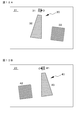
- FIG. 16A The result of simulating this state is shown in FIG. 16A.
- 16A, 16B and 17 show the case where the first A deflecting member 31, the first B deflecting member 32 and the first C deflecting member 33 constituting the first deflecting unit 30 are arranged in the state shown in FIG. That is, the simulation result is shown assuming that the first A deflection member 31 and the second A deflection member 41 are combined and the first B deflection member 32 and the second B deflection member 42 are arranged in a combined state. It is a figure.
- 10A and 10B are schematic diagrams showing the arrangement and second stage of the deflecting member 43. Further, a schematic view of the arrangement and the second stage of the first A deflecting member, the first B deflecting member and the first C deflecting member which constitute the optical device of Example 1, and the first A deflecting member and the first B in the disposing and the second stage.
- 11A and 11B are conceptual diagrams of wave number vectors and the like of the deflecting member and the 1C-th deflecting member.
- the first deflection unit 30 is arranged in a state of being rotated about the origin O in the first clockwise rotation direction by, for example, 7 degrees.
- the second deflection unit 40 is arranged in a state of being rotated about the origin O in the second counterclockwise rotation direction by, for example, 7 degrees (eg, ⁇ 7 degrees in the clockwise direction).
- the simulation result of the image obtained by such rotation is shown in FIG. 16B. It can be seen that the image moves in the +X-axis direction and the Y-axis direction as compared with FIG. 16A.
- the first deflection unit 30 includes a first A deflection member 31, a first B deflection member 32, and The wave number vector of the first C deflection member 33 may be rotated in the first clockwise rotation direction by, for example, 7 degrees.
- the second deflection unit 40 is configured as a second A unit.
- the wave number vectors of the deflecting member 41, the second B deflecting member 42, and the second C deflecting member 43 may be rotated in the second counterclockwise rotation direction by, for example, 7 degrees (eg, -7 degrees in the clockwise direction).
- the wave number vector of the first A deflection member 31 is k v 1-A ′′
- the X component, Y component, and Z component of k v 1-A ′′ are k X 1- A , k Y 1-A ′′, k Z 1-A ′′
- the wave number vector of the second A deflection member 41 is k v 2-A ′′
- the X component, Y component, and Z component of k v 2-A ′′ the wave number vector of the first A deflection member 31
- the X component, Y component, and Z component of k v 1-A ′′ are k X 1- A , k Y 1-A ′′, k Z 1-A ′′
- the wave number vector of the second A deflection member 41 is k v 2-A ′′
- the X component, Y component, and Z component of k v 2-A ′′ is k v 2-A ′′
- the wave number vector of the first B-deflecting member 32 is k v 1-B ′′
- the X component, Y component, and Z component of k v 1-B ′′ are k X 1-B ′′ and k Y 1-B ′′.
- the first deflection unit 30 is arranged in a state of being rotated about the Z axis in a counterclockwise or clockwise first rotation direction. Further, the second deflection unit 40 is arranged in a state of being rotated in the second rotation direction of the clockwise direction or the counterclockwise direction about the Z axis.
- the first deflection unit 30 is arranged in a state of being rotated by
- 7 degrees (+7 degrees) around the origin O in the first clockwise rotation direction.
- the second deflection unit 40 is arranged in a state of being rotated about the origin O in the second counterclockwise rotation direction by
- 7 degrees ( ⁇ 7 degrees).
- the first deflection unit 30 shown in FIG. 8A is arranged in a state of being rotated about the origin O in the first clockwise rotation direction by, for example, 7 degrees
- the second deflection unit 40 shown in FIG. 8B is arranged.
- the states shown in FIGS. 10A and 10B are obtained.
- “dropout” occurs in the image in the Y axis and its vicinity.
- a region where a dropout occurs in the image is shown by a region surrounded by a dotted line in FIGS. 10A and 10B.
- the first B deflection when the first B deflection member 32 is orthographically projected onto the first light guide plate 21 in each of the first B deflection member 32 and the second B deflection member 42, the first B deflection when the first B deflection member 32 is orthographically projected onto the first light guide plate 21.
- the member orthogonal projection image and the second B deflection member orthogonal projection image when the second B deflection member 42 is orthogonally projected onto the first light guide plate 21 are partially overlapped. Furthermore, the +X-axis direction end of the first B-deflecting member orthogonal projection image and the ⁇ X-axis direction end of the second B-deflecting member orthogonal projection image are overlapped.
- FIGS. 12A and 12B are schematic diagrams showing the arrangement and the second stage of the first deflection unit constituting the optical device of the first embodiment.
- the first B deflection member orthographic image is shown.
- the +X-axis direction end of the above is in contact with the ⁇ X-axis direction end of the orthographic image of the second B deflecting member.
- FIGS. 1A and 1B Schematic diagrams showing the arrangement and third stage of the deflecting member 43 are shown in FIGS. 1A and 1B.
- FIG. 2A shows a schematic diagram of the arrangement/third stage of the arrangement of the first A deflecting member, the first B deflecting member and the first C deflecting member constituting the optical device of Example 1, and the first A deflecting member in the disposing/third stage.
- 2B is a conceptual diagram of the wave number vectors of the first B deflecting member and the first C deflecting member.
- 90 degrees ⁇ 1 ⁇ 105 degrees 90 degrees ⁇ 2 ⁇ 105 degrees 90 degrees ⁇ 1 ⁇ 100 degrees 90 degrees ⁇ 2 ⁇ 100 degrees.
- first B deflecting member 32 and the second B deflecting member 42 are rotated, and the tilt angle (slant angle) ⁇ in the first B deflecting member 32 and the second B deflecting member 42, the pitch d of the lattice plane, and the incidence on the interference fringes.
- the first C deflection member 33 and the second C deflection member 43 are rotated, and the inclination angle (slant angle) ⁇ of the first C deflection member 33 and the second C deflection member 43, the pitch d of the lattice plane, and the angle of incidence on the interference fringes.
- the complementary angle ⁇ may be optimized.
- FIG. 17 shows a simulation result of an image obtained by rotating the deflecting members 32, 42, 33, 43 in this way.
- the FOV value in the +X-axis direction spreads, that is, It can be seen that the portion of the area in 16B (area D shown in white) is almost eliminated in FIG. 18A and 18B show results of simulating the propagation state of light in the first light guide plate 21 and the second light guide plate 22 obtained in the optical device of the first embodiment, and the first deflection unit 30 shown in FIG.
- the simulation results of the image obtained by the second deflection unit 40 are shown in FIGS. 19A and 19B.
- the wave vector of the first A deflection member 31 is k v 1-A
- the X component, Y component, and Z component of k v 1-A are k X 1-A , k Y 1-A and k Z 1-A
- the wave number vector of the second A deflection member 41 is k v 2-A
- the X component, Y component, and Z component of k v 2-A are k X 2-A.
- K Y 2-A , k Z 2-A , k X 1-A + k X 2-A 0
- k Y 1-A k Y 2-A
- k Z 1-A k Z 2-A Is.
- the wave number vector of the first C deflection member 33 is k v 1-C
- the X component, Y component, and Z component of k v 1-C are k X 1-C , k Y 1-C , and k Z 1- C
- the wave number vector of the second C deflection member 43 is k v 2-C
- the X, Y, and Z components of k v 2-C are k X 2-C , k Y 2-C
- k Z 2 -C k X 1-C + k X 2-C 0
- k Y 1-C k Y 2-C
- k Z 1-C k Z 2-C Is.
- the wave number vector of the first B deflection member 32 is k v 1-B
- the X component, Y component, and Z component of k v 1-B are k X 1-B , k Y 1-B , and k Z 1 -B
- the wave number vector of the second B-deflecting member 42 is k v 2-B
- the X component, Y component, and Z component of k v 2-B are k X 2-B , k Y 2-B , and k Z.
- the triangle formed by the conceptually illustrated wave number vectors k v 1-A , k v 1-B , and k v 1-C is an isosceles triangle, and the triangles of
- the value of the grating period d 1 is, for example, 335.00 nm
- the value of the grating period d 2 of the first B deflecting member or the like is, for example, 359.26 nm
- the value of the grating period d 3 of the first C deflecting member or the like Is, for example, 384.22 nm.
- the average diffraction efficiency of the first A deflecting member 31 with respect to the light emitted from the image forming apparatus 60 is ⁇ 1-A
- the average diffraction efficiency of the first B deflecting member 32 is ⁇ 1-B
- the average diffraction efficiency of the first C deflecting member 33 is.
- the average diffraction efficiency of the member 41 is ⁇ 2-A
- the average diffraction efficiency of the second B deflecting member 42 is ⁇ 2-B
- the average diffraction efficiency of the second C deflecting member is ⁇ 2-C
- the image forming apparatus 60 (hereinafter, the image forming apparatus shown in FIG. 6A is referred to as an image forming apparatus 60A) is the image forming apparatus of the first configuration, and is a plurality of two-dimensional matrix arranged. Of pixels.
- the image forming apparatus 60A includes a reflective spatial light modulator and a light source 71 including a light emitting diode (LED) that emits white light.
- the entire image forming apparatus 60A is housed in a housing 70 (indicated by a dashed line in FIG. 6A), and the housing 70 is provided with an opening (not shown). Light is emitted from the optical system (parallel light emitting optical system, collimating optical system) 74 via the optical system.
- the housing 70 is attached to the upper portion of the front portion 51 by an attachment member (not shown).
- the reflective spatial light modulator consists of a liquid crystal display (LCD) 73 consisting of LCOS as a light valve. Further, a polarization beam splitter that reflects a part of the light from the light source 71 and guides it to the liquid crystal display device 73, and passes a part of the light reflected by the liquid crystal display device 73 and guides it to the optical system 74. 72 are provided.
- the liquid crystal display device 73 includes a plurality of (for example, 640 ⁇ 480) pixels (liquid crystal cells, liquid crystal display elements) arranged in a two-dimensional matrix.
- the polarization beam splitter 72 has a known configuration and structure.
- the non-polarized light emitted from the light source 71 collides with the polarization beam splitter 72.
- the P-polarized component passes and is emitted outside the system.
- the S-polarized component is reflected by the polarization beam splitter 72, enters the liquid crystal display device 73, is reflected inside the liquid crystal display device 73, and is emitted from the liquid crystal display device 73.
- the light emitted from the liquid crystal display device 73 the light emitted from the pixel displaying “white” contains a large amount of P-polarized component, and the light emitted from the pixel displaying “black” is S-polarized. Contains a lot of ingredients.
- the P-polarized component passes through the polarization beam splitter 72 and is guided to the optical system 74.
- the S polarization component is reflected by the polarization beam splitter 72 and returned to the light source 71.
- the optical system 74 is composed of, for example, a convex lens, and the image forming apparatus 60A (more specifically, the liquid crystal display device 73) is arranged at a position (position) of the focal length in the optical system 74 in order to generate parallel light. Has been done.
- the image emitted from the image forming apparatus 60A is incident on the first A deflecting member 31 and the second A deflecting member 41 via a light guide unit (not shown).
- the liquid crystal display device 73 includes a plurality of (for example, 640 ⁇ 480) pixels (liquid crystal cells, liquid crystal display elements) arranged in a two-dimensional matrix.
- the image forming apparatus 60 (hereinafter, the image forming apparatus shown in FIG. 6B is referred to as an image forming apparatus 60B) includes an organic EL display device 75.
- the image emitted from the organic EL display device 75 passes through the convex lens 76, becomes parallel light, and travels toward the first A deflection member 31 and the second A deflection member 41 via a light guide unit (not shown).
- the organic EL display device 75 includes a plurality of (for example, 640 ⁇ 480) pixels (organic EL elements) arranged in a two-dimensional matrix.
- the image forming apparatus 60 which is the image forming apparatus having the second configuration (hereinafter, the image forming apparatus shown in FIG. 6C is referred to as an image forming apparatus 60C) is Light source 81, A collimating optical system 82 for collimating the light emitted from the light source 81, Scanning means 84 for scanning the parallel light emitted from the collimating optical system 82, and A relay optical system 85 for relaying and emitting parallel light scanned by the scanning means 84, It consists of The entire image forming apparatus 60C is housed in a housing 70 (indicated by a chain line in FIG. 6C), and the housing 70 is provided with an opening (not shown).
- the housing 70 is attached to the upper portion of the front portion 51 by an attachment member (not shown).
- the light source 81 is composed of a light emitting element (LED) that emits green light. Then, the light emitted from the light source 81 enters the collimating optical system 82 having a positive optical power as a whole and is emitted as parallel light. Then, the parallel light is reflected by the total reflection mirror 83, makes the micromirror rotatable in the two-dimensional direction, and performs horizontal scanning and scanning by the scanning means 84 composed of the MEMS capable of two-dimensionally scanning the incident parallel light.
- the light from the virtual pixel passes through a relay optical system (parallel light emitting optical system) 85 composed of a well-known relay optical system, and passes through a light guide means (not shown) to the first A deflection member 31 and the The light enters the 2A deflection member 41.
- a relay optical system parallel light emitting optical system
- the optical device is provided with one image forming device 60 (60A, 60B, 60C), and the image emitted from the image forming device 60 can be transferred to the lenses 74, 76, 85 (see drawings). (Indicated by reference numeral 101 in FIG. 1), and may be incident on the first A deflection member 31 and the second A deflection member 41. The image emitted from the image forming apparatus 60 is incident on the first A deflection member 31 and the second A deflection member 41 via the lens 101.
- the entrance pupil diameter of the lens 101 in the X-axis direction is preferably larger than the widths of the first A deflection member 31 and the second A deflection member 32 in the X axis direction, and the first A deflection member 31 and the second A deflection member 32 are included. It is more preferable that the width is the same as the width in the X-axis direction.
- the deflecting members other than the first A deflecting member 31, the second A deflecting member 41, and the light guide plates 21 and 22 are omitted.
- a frame 50 constituting the display device is rotatably attached to a front portion 51 (having a rim 51′) arranged in front of an observer, and hinges 52 at both ends of the front portion 51.
- the nose pad 51′′ is attached. That is, the assembly of the frame 50 and the nose pad 51′′ basically has substantially the same structure as ordinary glasses.
- each housing 70 is attached to the front portion 51 by an attachment member (not shown).
- the frame 50 is made of metal or plastic.
- Each housing 70 may be detachably attached to the front portion 51 by an attachment member.
- wirings (signal lines, power lines, etc., some of which are not shown) 55 extending from one image forming apparatus 60 are connected to the modern portion via the inside of the temple portion 53 and the modern portion 54. It extends from the tip of 54 to the outside and is connected to a control device (control circuit, control means) 58.
- each image forming apparatus 60 is provided with a headphone section 56, and a headphone section wiring 57 extending from each image forming apparatus 60 is connected to the temple section 53 and the modern section 54 via the interior of the modern section 54. It extends from the tip to the headphone section 56.
- the headphone wiring 57 (a part of which is not shown) extends from the front end of the modern portion 54 to the headphone portion 56 so as to wrap around the back side of the auricle (auricle). ing. With such a configuration, it is possible to provide a neat display device without giving the impression that the headphones 56 and the headphones wiring 57 are randomly arranged.
- the optical device of the first embodiment, the optical device that constitutes the image display device of the first embodiment, and the optical device that constitutes the display device of the first embodiment are the first deflection unit provided on the first light guide plate and the second light guide plate. And a second deflection unit, and a part (for example, half) of the image emitted from the image forming apparatus is incident on the first deflection unit, and at least the remaining portion (for example, the remaining portion) of the image emitted from the image forming apparatus. Half of that) is incident on the second deflection unit. That is, the image is divided into a kind by the first A deflection member and the second A deflection member.
- these divided images are finally emitted from the first deflection unit and the second deflection unit and combined, that is, the images emitted from the first C deflection member and the second C deflection member are combined.
- the first direction and the second direction are opposite directions and are not parallel, it is possible to further widen the angle of view.
- the first deflection unit and the first deflection unit are provided in one light guide plate instead of the first light guide plate and the second light guide plate, the light is diffracted and reflected by the first deflection unit and totally reflected inside the light guide plate.
- the first deflection unit is provided on the first light guide plate and the second deflection unit is provided on the second guide unit.
- Example 2 is a modification of Example 1.
- Example 1 it is assumed that the +X axis and the ⁇ X axis are located in the horizontal plane.
- the +X axis and the ⁇ X axis are located in the vertical plane.
- 13 and 14 are schematic diagrams of the first light guide plate and the first deflection unit, and the second light guide plate and the second deflection unit that configure the optical device of the second embodiment.
- 13 and 14 are conceptual views of an optical device that constitutes the image display device for the right eye as viewed from the front.
- the observer's ear is located on the right hand side of the figure and the observer's ear is on the left hand side of the figure.
- the nose is located.
- the observer's nose is located in the Y-axis (specifically, -Y axis) direction
- the observer's ear is located in the Y-axis (specifically, +Y axis) direction.
- the light that has entered the light guide plate travels in a substantially horizontal direction from the first A deflecting member and the second A deflecting member toward the first B deflecting member and the second B deflecting member (that is, the Y axis is located in the horizontal direction).
- the optical device of Example 2 can have the same configuration and structure as the optical device of Example 1, and thus detailed description thereof will be omitted. Whether to adopt the first embodiment or the second embodiment may be determined based on the specifications required for the optical device, the image display device, and the display device.
- the deflecting member may be a reflective blazed diffraction grating element.
- the display device of the present disclosure can also be used as a stereoscopic display device. In this case, a polarizing plate or a polarizing film may be removably attached to the optical device or a polarizing plate or a polarizing film may be attached to the optical device, if necessary.
- the image display device may include a light control device. That is, the optical device may overlap at least a portion of the dimmer. More specifically, it is preferable that at least the first C deflecting member and the like of the optical device overlap with the light control device.
- the first A deflection member and the like and the first B deflection member and the like may be formed, or the first A deflection member and the first C deflection member and the like may be formed on the material forming one volume hologram diffraction grating.
- the first B deflecting member or the like and the first C deflecting member or the like may be formed, or the first A deflecting member or the like, the first B deflecting member or the like, the first C deflecting member or the like and the first B deflecting member or the like may be formed. May be.
- the hologram area may be formed on the light guide plate by an imprint method or an etching method.
- FIGS. 15A, 15B, 15C, 15D, 15E, 15F, 15G, and 15H conceptual diagrams of modified examples of the optical device described in Example 1. It can be deformed. That is, as shown in FIG. 15A, the first A deflecting member 31a composed of a transmission type volume hologram diffraction grating is arranged on the first surface of the light guide plate, and the first A deflection member 31a composed of a reflection type volume hologram diffraction grating is arranged on the second surface of the light guide plate.
- the 1B deflection member or the like 32b and the first C deflection member or the like 33b may be arranged.
- FIG. 15A the first A deflecting member 31a composed of a transmission type volume hologram diffraction grating is arranged on the first surface of the light guide plate
- the first A deflection member 31a composed of a reflection type volume hologram diffraction grating
- a first B deflection member or the like 32a and a first C deflection member 33a which are transmission type volume hologram diffraction gratings, are arranged on the first surface of the light guide plate, and are reflected on the second surface of the light guide plate.
- a first A deflecting member 31b composed of a die volume hologram diffraction grating may be arranged.
- a first A deflection member or the like 31a, a first B deflection member or the like 32a, and a first C deflection member or the like 33a which are transmission volume hologram diffraction gratings may be arranged on the first surface of the light guide plate. Good.
- the first surface A of the light guide plate is provided with the first A deflection member 31a composed of a transmission type volume hologram diffraction grating, and the second surface of the light guide plate is composed of a reflection type volume hologram diffraction grating.
- the first A deflection member or the like 31b, the first B deflection member or the like 32b, and the first C deflection member or the like 33b may be arranged.
- FIG. 15D the first surface A of the light guide plate is provided with the first A deflection member 31a composed of a transmission type volume hologram diffraction grating
- the second surface of the light guide plate is composed of a reflection type volume hologram diffraction grating.
- the first A deflection member or the like 31b, the first B deflection member or the like 32b, and the first C deflection member or the like 33b may be arranged.
- a first A deflection member or the like 31a, a first B deflection member or the like 32a and a first C deflection member or the like 33a which are transmission volume hologram diffraction gratings, are arranged on the first surface of the light guide plate to guide the light.
- a first B deflection member or the like 32a and a first C deflection member 33a which are transmission type volume hologram diffraction gratings, are arranged on the first surface of the light guide plate, and are reflected on the second surface of the light guide plate.
- the first A deflecting member 31b, the first B deflecting member 32b, and the first C deflecting member 33b which are formed by a volume hologram hologram, may be arranged. Alternatively, as shown in FIG.
- the first A deflection member 31a, the first B deflection member 32a, and the first C deflection member 33a which are transmission volume hologram diffraction gratings, are arranged on the first surface of the light guide plate to guide the light.
- the first B deflecting member 32b and the first C deflecting member 33b which are reflection type volume hologram diffraction gratings, may be arranged on the second surface of the optical plate.
- the first A deflecting member 31a, the first B deflecting member 32a, and the first C deflecting member 33a which are transmission volume hologram diffraction gratings, are arranged on the first surface of the light guide plate to guide the light. You may arrange
- the dimmer is First substrate, A second substrate facing the first substrate, A first transparent electrode provided on a surface of the first substrate facing the second substrate, A second transparent electrode provided on a surface of the second substrate facing the first substrate, and A light control layer sandwiched between a first transparent electrode and a second transparent electrode, It may be in the form of In addition, when the light control device is operating, or when the light control device is operating, for example, a voltage higher than that of the second transparent electrode is applied to the first transparent electrode.
- the light control layer may be formed of an optical shutter that applies a color change of a substance generated by a redox reaction of an inorganic or organic electrochromic material.
- the light control layer may be in a form containing an inorganic or organic electrochromic material, and further, the light control layer may include a WO 3 layer/Ta 2 O 5 layer/from the first transparent electrode side. It may have a laminated structure of an inorganic electrochromic material layer such as an Ir X Sn 1 -X O layer or a laminated structure of an inorganic electrochromic material layer such as a WO 3 layer/Ta 2 O 5 layer/IrO x layer. it can.
- a MoO 3 layer or a V 2 O 5 layer can be used instead of the WO 3 layer.
- a ZrO 2 layer instead of the IrO x layer, a ZrO 2 layer, a zirconium phosphate layer can be used, or a Prussian blue complex/nickel-substituted Prussian blue complex can also be used.
- the organic electrochromic material for example, the electrochromic materials disclosed in JP-A-2014-111710 and JP-A-2014-159385 can be used.
- the light control layer may be in a form containing an electrophoretic dispersion liquid, and the light control device may be applied with an electrodeposition/dissociation phenomenon generated by a reversible redox reaction of a metal (for example, silver particles).
- a metal for example, silver particles.
- the optical shutter by the electrodeposition method electrodeposition/electric field deposition
- the light control layer may be in a form including an electrolyte containing metal ions.
- the electrophoretic dispersion liquid is composed of a large number of charged electrophoretic particles and a dispersion medium of a color different from that of the electrophoretic particles.
- the first transparent electrode is patterned and the second transparent electrode is not patterned (so-called solid electrode configuration)
- the electrophoretic particles are negatively charged, relative to the first transparent electrode.
- the negatively charged electrophoretic particles migrate so as to cover the second transparent electrode. Therefore, the light blocking ratio in the light control device has a high value.
- the electrophoretic particles cover the first transparent electrode. Run. Therefore, the light blocking ratio in the light control device has a low value.
- the voltage may be direct current or alternating current.
- the shape of the patterned first transparent electrode is the optimum value of the light blocking rate in the light control device when the electrophoretic particles migrate so as to cover the first transparent electrode and the light blocking rate in the light control device becomes a low value. The shape may be such that it can be realized, and various tests may be performed to determine it.
- an insulating layer may be formed on the transparent electrode.
- the material forming the insulating layer include, for example, colorless and transparent insulating resin, and specifically, for example, acrylic resin, epoxy resin, fluorine resin, silicone resin, polyimide resin, Examples thereof include polystyrene resin.
- a transparent glass substrate such as soda lime glass or white plate glass
- a plastic substrate such as soda lime glass or white plate glass
- a plastic substrate such as soda lime glass or white plate glass
- a plastic sheet such as soda lime glass or white plate glass
- a plastic film such as soda lime glass or white plate glass
- the plastic polyethylene terephthalate, polyethylene naphthalate, polycarbonate, cellulose ester such as cellulose acetate, fluoropolymer such as polyvinylidene fluoride or a copolymer of polytetrafluoroethylene and hexafluoropropylene, polyoxymethylene and the like Ether, polyacetal, polystyrene, polyethylene, polypropylene, polyolefin such as methylpentene polymer, polyimide such as polyamide imide or polyether imide, polyamide, polyether sulfone, polyphenylene sulfide, polyvinylidene fluoride, tetraacetyl
- the plastic sheet or the plastic film may have rigidity that does not easily bend or may have flexibility.
- a barrier layer made of an inorganic material or an organic material may be formed on the inner surface of the substrates.
- the first substrate and the second substrate are sealed and adhered by a sealing member at the outer edge.
- a sealing member also called a sealing agent
- a thermosetting type such as an epoxy resin, a urethane resin, an acrylic resin, a vinyl acetate resin, an ene-thiol resin, a silicone resin, a modified polymer resin
- Various resins such as moisture-curing type and anaerobic-curing type can be used.
- one of the substrates constituting the light control device also serves as a component member of the optical device (specifically, a protective member disposed so that the volume hologram diffraction grating does not come into direct contact with the atmosphere), the entire display device is provided.
- the weight of the display device can be reduced, and the user of the display device does not feel uncomfortable.
- the other substrate may be thinner than the one substrate.
- the first transparent electrode may be patterned or may not be patterned.
- the second transparent electrode may be patterned or may not be patterned.
- indium-tin composite oxide including ITO, Indium Tin Oxide, Sn-doped In 2 O 3 , crystalline ITO and amorphous ITO
- FTO Fluorine-doped SnO 2
- IFO Fluorine-doped In 2 O 3
- indium-zinc composite examples thereof include oxides (IZO, Indium Zinc Oxide), spinel type oxides, oxides having a YbFe 2 O 4 structure, and conductive polymers such as polyaniline, polypyrrole, and polythiophene, but are not limited thereto.
- the first transparent electrode and the second transparent electrode are formed based on a physical vapor deposition method (PVD method) such as a vacuum deposition method or a sputtering method, various chemical vapor deposition methods (CVD method), various coating methods, and the like.
- PVD method physical vapor deposition method
- CVD method chemical vapor deposition methods
- the patterning can be performed by any method such as an etching method, a lift-off method, and a method using various masks.
- the dimmer can be configured to be installed in the front part. Further, in this case, the front portion has a rim; the light control device can be configured to be fitted into the rim. Further, in the display device of the present disclosure including the various preferable forms described above, the optical device and the light control device may be arranged in this order from the viewer side, or the light control device and the optical device may be arranged in this order. Good.
- an illuminance sensor for measuring the illuminance of the environment where the display device is placed is further provided; a mode for controlling the light-shielding rate of the dimmer based on the measurement result of the illuminance sensor (environmental illuminance measurement sensor)
- the image forming apparatus further includes an illuminance sensor (environmental illuminance measurement sensor) that measures the illuminance of the environment in which the display device is placed; based on the measurement result of the illuminance sensor (environmental illuminance measurement sensor). It can be configured to control the brightness of the image. You may combine these forms.
- a second illuminance sensor (which may be referred to as a “transmitted light illuminance measurement sensor” for convenience) that measures illuminance based on light transmitted through the dimmer from an external environment is further provided; Based on the measurement result of the (transmitted light illuminance measurement sensor), the light blocking rate of the light control device can be controlled.
- it further comprises a second illuminance sensor (transmitted light illuminance measurement sensor) for measuring illuminance based on light transmitted through the light control device from the external environment; measurement result of the second illuminance sensor (transmitted light illuminance measurement sensor). Based on the above, the brightness of the image formed by the image forming apparatus can be controlled.
- the second illuminance sensor (transmitted light illuminance measurement sensor) is preferably arranged on the observer side of the optical device. At least two second illuminance sensors (transmitted light illuminance measurement sensors) are arranged to measure illuminance based on light that has passed through a portion with a high light blocking rate and illuminance based on light that has passed through a portion with a low light blocking rate. You can go. You may combine these forms. Furthermore, these forms may be combined with a form in which control is performed based on the measurement result of the above-mentioned illuminance sensor (environmental illuminance measurement sensor).
- the illuminance sensor (environmental illuminance measurement sensor, transmitted light illuminance measurement sensor) may be composed of a known illuminance sensor, and the illuminance sensor may be controlled based on a known control circuit.
- the maximum light transmittance of the light control device may be 50% or more, and the minimum light transmittance of the light control device may be 30% or less.
- the upper limit of the maximum light transmittance of the light control device can be 99%, and the lower limit of the minimum light transmittance of the light control device can be 1%.
- (Light transmittance) 1-(Light blocking rate) Have a relationship.
- a connector is attached to the dimmer (specifically, a connector is attached to the first transparent electrode and the second transparent electrode), and a control circuit for controlling the light blocking rate of the dimmer (the dimmer/control circuit. , For example, it is included in a control device for controlling the image forming apparatus), and the light control device may be electrically connected via this connector and wiring.
- the light passing through the light control device may be colored in a desired color by the light control device.
- the color colored by the light control device can be variable, or the color colored by the light control device can be fixed.
- a light control device colored red, a light control device colored green, and a light control device colored blue may be stacked.
- the color to be colored by the light control device may be, but not limited to, brown.
- an observer observes the brightness of light that has passed through the light control device and the optical device, and the observer manually controls and adjusts the light blocking rate by operating switches, buttons, dials, sliders, knobs, etc.
- the shading rate is controlled and adjusted based on the measurement result of the second illuminance sensor (transmitted light illuminance measurement sensor) that measures the illuminance based on the light transmitted through the light control device from the external environment.
- the control and adjustment of the light blocking rate may be performed by specifically controlling the voltage applied to the first transparent electrode and the second transparent electrode.
- At least two second illuminance sensors are arranged to measure illuminance based on light that has passed through a portion with a high light blocking rate and illuminance based on light that has passed through a portion with a low light blocking rate. You can go.
- the display device may include one image display device or two image display devices. When two image display devices are provided, one of the light control devices and the other of the light control devices each adjust the voltage applied to the first transparent electrode and the second transparent electrode, thereby adjusting one of the light control devices. It is possible to equalize the light blocking rate in (4) and the light blocking rate in the other light control device.
- the light blocking rate in one light control device and the light blocking rate in the other light control device are, for example, a second illuminance sensor (transmitted light illuminance measurement sensor) that measures the illuminance based on the light transmitted through the light control device from the external environment described above. It is possible to control the brightness of the light passing through one of the dimmers and the optical device and the brightness of the light passing through the other dimmer and the optical device. It is also possible for the observer to manually control and adjust by operating switches, buttons, dials, sliders, knobs, etc. When adjusting the light blocking ratio, a test pattern may be displayed on the optical device.
- a test pattern may be displayed on the optical device.
- the first deflection unit includes a first A deflection member, a first B deflection member and a first C deflection member
- the second deflection unit is composed of a second A deflection member, a second B deflection member and a second C deflection member, Part of the light emitted from the image forming apparatus is incident on the first A deflection member, The light incident on the first A deflecting member is deflected by the first A deflecting member, is totally reflected inside the first light guide plate, enters the first B deflecting member, is deflected by the first B deflecting member, and is reflected by the first light guide plate.
- the light is totally reflected inside and enters the first C deflecting member, is deflected by the first C deflecting member, and is emitted toward the observer's pupil. At least the remaining part of the light emitted from the image forming apparatus is incident on the second A deflection member, The light incident on the second A deflecting member is deflected by the second A deflecting member, is totally reflected inside the second light guide plate, is incident on the second B deflecting member, is deflected by the second B deflecting member, and is reflected by the second light guide plate. The light is totally reflected inside and is incident on the second C deflecting member, is deflected by the second C deflecting member, and is emitted toward the observer's pupil.
- Propagation direction of the light deflected by the first B-deflecting member in the first light guide plate is the first direction when the projection direction is orthogonal to the first light guide plate, and propagation of light deflected by the second B-deflecting member in the second light guide plate.
- An optical device in which the first direction is opposite to the second direction when the direction when the direction is orthogonally projected onto the first light guide plate is the second direction.
- An origin is a point on the first light guide plate where a light beam emitted from the center point of the image forming area of the image forming apparatus collides with the first light guide plate,
- the bisector of an acute intersection angle is The axis containing the bisector going toward is the +X axis,
- the Z axis is the axis that passes through the origin and is perpendicular to the first light guide plate.
- the first deflection unit and the second deflection unit are the optical device according to [A01] or [A02], which are arranged at positions symmetrical with respect to the YZ plane.
- the first deflection unit is arranged in a state of being rotated about the Z axis in the counterclockwise or clockwise first rotation direction
- the bisector of an acute intersection angle is The axis containing the bisector going toward is the +X axis,
- the Z axis is the axis that passes through the origin and is perpendicular to the first light guide plate.
- the angle ( ⁇ X ) formed by the orthogonal projection image and the X axis when the light ray emitted from the center point of the image forming area of the image forming apparatus and incident on the origin is orthographically projected onto the first light guide plate is less than 90 degrees [ The optical device according to any one of A01] to [A09].
- the optical device according to [A10] which satisfies: [A12]
- the angle ( ⁇ X ) formed by the orthogonal projection image and the Y-axis when the ray emitted from the center point of the image forming area of the image forming apparatus and incident on the origin is orthogonally projected on the YZ plane is ⁇ 20 degrees or more.
- the first A deflecting member and the second A deflecting member are composed of a volume hologram diffraction grating,
- the wave vector of the first A deflection member is k v 1-A, and the X component, Y component, and Z component of k v 1-A are k X 1-A , k Y 1-A , and k Z 1-A
- the wave number vector of the second A deflection member is k v 2-A
- the X component, Y component, and Z component of k v 2-A are k X 2-A , k Y 2-A , and k Z 2-A .
- the optical device according to any one of [A03] to [A14], which satisfies: [A16]
- the first C deflecting member and the second C deflecting member are composed of a volume hologram diffraction grating,
- the wave number vector of the first C deflection member is k v 1-C, and the X component, Y component, and Z component of k v 1-C are k X 1-C , k Y 1-C , and k Z 1-C
- the wave number vector of the second C deflection member is k v 2-C, and the X component, Y component, and Z component of k v 2-C are k X 2-C , k Y 2-C , and k Z 2-C .
- the optical device which satisfies: [A17]
- the first B deflecting member and the second B deflecting member are composed of a volume hologram diffraction grating,
- the wave vector of the first B-deflecting member is k v 1-B, and the X component, Y component, and Z component of k v 1-B are k X 1-B , k Y 1-B , and k Z 1-B
- the wave number vector of the second B-deflecting member is k v 2-B, and the X, Y, and Z components of k v 2-B are k X 2-B , k Y 2-B , and k Z 2-B .
- the first A deflecting member, the first B deflecting member, and the first C deflecting member are composed of a volume hologram diffraction grating,
- the average diffraction efficiency of the first A deflection member with respect to the light emitted from the image forming apparatus is ⁇ 1-A
- the average diffraction efficiency of the first B deflection member is ⁇ 1-B
- the average diffraction efficiency of the first C deflection member is ⁇ 1-C.
- the second A deflecting member, the second B deflecting member and the second C deflecting member are composed of a volume hologram diffraction grating,
- the average diffraction efficiency of the second A deflection member with respect to the light emitted from the image forming apparatus is ⁇ 2-A
- the average diffraction efficiency of the second B deflection member is ⁇ 2-B
- the average diffraction efficiency of the second C deflection member is ⁇ 2-C.
- the optical device includes a first light guide plate and a second light guide plate, and a first deflection unit provided on the first light guide plate and a second deflection unit provided on the second light guide plate,
- the first deflection unit includes a first A deflection member, a first B deflection member and a first C deflection member
- the second deflection unit is composed of a second A deflection member, a second B deflection member and a second C deflection member, Part of the light emitted from the image forming apparatus is incident on the first A deflection member, The light incident on the first A deflecting
- the light is totally reflected inside and enters the first C deflecting member, is deflected by the first C deflecting member, and is emitted toward the observer's pupil. At least the remaining part of the light emitted from the image forming apparatus is incident on the second A deflection member, The light incident on the second A deflecting member is deflected by the second A deflecting member, is totally reflected inside the second light guide plate, is incident on the second B deflecting member, is deflected by the second B deflecting member, and is reflected by the second light guide plate. The light is totally reflected inside and is incident on the second C deflecting member, is deflected by the second C deflecting member, and is emitted toward the observer's pupil.
- Propagation direction of the light deflected by the first B-deflecting member in the first light guide plate is the first direction when the projection direction is orthogonal to the first light guide plate, and propagation of light deflected by the second B-deflecting member in the second light guide plate.
- An image display device in which the first direction is opposite to the second direction when the direction when the direction is orthographically projected onto the first light guide plate is the second direction.
- a display device >> A frame attached to the observer's head, and Image display device attached to the frame, A display device comprising: The image display device includes an image forming device, and an optical device into which light emitted from the image forming device is incident, guided, and emitted.
- the optical device includes a first light guide plate and a second light guide plate, and a first deflection unit provided on the first light guide plate and a second deflection unit provided on the second light guide plate
- the first deflection unit includes a first A deflection member, a first B deflection member and a first C deflection member
- the second deflection unit is composed of a second A deflection member, a second B deflection member and a second C deflection member, Part of the light emitted from the image forming apparatus is incident on the first A deflection member,
- the light incident on the first A deflecting member is deflected by the first A deflecting member, is totally reflected inside the first light guide plate, enters the first B deflecting member, is deflected by the first B deflecting member, and is reflected by the first light guide plate.
- the light is totally reflected inside and enters the first C deflecting member, is deflected by the first C deflecting member, and is emitted toward the observer's pupil. At least the remaining part of the light emitted from the image forming apparatus is incident on the second A deflection member, The light incident on the second A deflecting member is deflected by the second A deflecting member, is totally reflected inside the second light guide plate, is incident on the second B deflecting member, is deflected by the second B deflecting member, and is reflected by the second light guide plate. The light is totally reflected inside and is incident on the second C deflecting member, is deflected by the second C deflecting member, and is emitted toward the observer's pupil.
- Propagation direction of the light deflected by the first B-deflecting member in the first light guide plate is the first direction when the projection direction is orthogonal to the first light guide plate, and propagation of light deflected by the second B-deflecting member in the second light guide plate.
- a display device in which the first direction is opposite to the second direction when the direction when the direction is orthographically projected onto the first light guide plate is the second direction.
- Image forming apparatus 70... Housing, 71... Light source, 72... Polarizing beam splitter (PBS), 73... Liquid crystal display (LCD), 74... Optical system (parallel light emitting optical system, collimating optical system), 75... Organic EL display device, 76... Convex lens, 81... Light source, 82... Collimating optical system, 83... Total reflection mirror , 84... Scanning means, 85... Relay optical system, 90... Observer's pupil
Landscapes
- Physics & Mathematics (AREA)
- General Physics & Mathematics (AREA)
- Optics & Photonics (AREA)
- Diffracting Gratings Or Hologram Optical Elements (AREA)
Abstract
Description
(A)2次元マトリクス状に配列された複数の画素を備えた画像形成装置、
(B)画像形成装置の画素から出射された光を平行光とするコリメート光学系、及び、
(C)コリメート光学系にて進行方位の異なる複数の平行光とされた光が入射され、導光され、出射される光学装置、
を備えた画像表示装置であって、
光学装置は、
(a)入射された光が内部を全反射により伝播した後、出射される導光板、
(b)導光板に入射された光が導光板の内部で全反射されるように、導光板に入射された光を回折反射する、反射型体積ホログラム回折格子から成り、導光板に配設された第1回折格子部材、及び、
(c)導光板の内部を全反射により伝播した光を回折反射し、導光板から出射する、反射型体積ホログラム回折格子から成り、導光板に配設された第2回折格子部材、
を備えており、
第1回折格子部材の中心を原点とし、原点を通る第1回折格子部材の法線であって、コリメート光学系側に向かう方向を正方向とする法線をXi軸、原点を通り、Xi軸と直交し、第2回折格子部材側に向かう方向を正方向とする導光板の軸線をYi軸としたとき、
画像形成装置の中心の画素から出射され、コリメート光学系の中心を通過する中心光は、XiYi平面に対して光学的に平行であり、且つ、XiZi平面に対して鋭角にて交わっていることを特徴とする画像表示装置が開示されている。
画像形成装置から出射された光が入射され、導光され、出射される光学装置であって、
第1導光板及び第2導光板、並びに、第1導光板に設けられた第1偏向ユニット及び第2導光板に設けられた第2偏向ユニットを備えており、
第1偏向ユニットは、第1A偏向部材、第1B偏向部材及び第1C偏向部材から構成されており、
第2偏向ユニットは、第2A偏向部材、第2B偏向部材及び第2C偏向部材から構成されており、
第1A偏向部材には、画像形成装置から出射された光の一部が入射され、
第1A偏向部材に入射した光は、第1A偏向部材によって偏向され、第1導光板の内部で全反射されて第1B偏向部材に入射し、第1B偏向部材によって偏向され、第1導光板の内部で全反射されて第1C偏向部材に入射し、第1C偏向部材によって偏向され、観察者の瞳に向けて出射され、
第2A偏向部材には、画像形成装置から出射された光の少なくとも残部が入射され、
第2A偏向部材に入射した光は、第2A偏向部材によって偏向され、第2導光板の内部で全反射されて第2B偏向部材に入射し、第2B偏向部材によって偏向され、第2導光板の内部で全反射されて第2C偏向部材に入射し、第2C偏向部材によって偏向され、観察者の瞳に向けて出射され、
第1B偏向部材によって偏向された光の第1導光板における伝播方向を第1導光板へ正射影したときの方向を第1方向、第2B偏向部材によって偏向された光の第2導光板における伝播方向を第1導光板へ正射影したときの方向を第2方向としたとき、第1方向は第2方向と反対方向である。
画像形成装置、及び、
画像形成装置から出射された光が入射され、導光され、出射される光学装置、
を備えた画像表示装置であって、
光学装置は、本開示の光学装置から成る。
観察者の頭部に装着されるフレーム、及び、
フレームに取り付けられた画像表示装置、
を備えた表示装置であって、
画像表示装置は、画像形成装置、及び、画像形成装置から出射された光が入射され、導光され、出射される光学装置を備えており、
光学装置は、本開示の光学装置から成る。
1.本開示の光学装置、画像表示装置及び表示装置、全般に関する説明
2.実施例1(本開示の光学装置、画像表示装置及び表示装置)
3.実施例2(実施例1の変形)
4.その他
本開示の光学装置、本開示の画像表示装置を構成する光学装置、本開示の表示装置を構成する光学装置(以下、これらを総称して、『本開示の光学装置等』と呼ぶ場合がある)において、第1導光板と第2導光板とは並置されている構成とすることができる。即ち、第1導光板と第2導光板とは、例えば、空気層を介して、離間して平行に配置されている構成とすることができる。
画像形成装置の画像形成領域中心点から出射された光線が第1導光板と衝突する第1導光板上の点を原点とし、
原点を通るXYZ直交座標系において、
原点を通り、第1方向に平行な直線と、原点を通り、第2方向に平行な直線とが交差する交差角度のうち、鋭角の交差角度の二等分線であって、第1方向に向かう二等分線を含む軸を+X軸とし、
原点を通り、第1導光板に垂直な軸をZ軸とし、
X軸及びZ軸と直交する軸をY軸としたとき、
第1偏向ユニットと第2偏向ユニットとは、YZ平面に対称な位置に配置されている形態とすることができる。
第1偏向ユニットは、Z軸を中心として、反時計方向又は時計方向の第1回転方向に回転した状態で配置されており、
第2偏向ユニットは、Z軸を中心として、時計方向又は反時計方向の第2回転方向に回転した状態で配置されている構成とすることができる。そして、この場合、+X軸を基準として、第1回転方向への回転角度をφ1、第2回転方向への回転角度をφ2としたとき、
|φ1|=|φ2|
を満足する形態とすることができ、更には、
0(度)<|φ1|=|φ2|≦23(度)
好ましくは、
0(度)<|φ1|=|φ2|≦16(度)
を満足する形態とすることができる。尚、第1偏向ユニットを第1回転方向に回転した状態で配置する代わりに、第1偏向ユニットを構成する第1A偏向部材、第1B偏向部材及び第1C偏向部材の波数ベクトルを第1回転方向に回転した状態としてもよいし、第2偏向ユニットを第2回転方向に回転した状態で配置する代わりに、第2偏向ユニットを構成する第2A偏向部材、第2B偏向部材及び第2C偏向部材の波数ベクトルを第2回転方向に回転した状態としてもよい。
90度<ψ1
90度<ψ2
を満足する形態とすることができ、更には、
90度<ψ1≦105度
90度<ψ2≦105度
好ましくは、
90度<ψ1≦100度
90度<ψ2≦100度
を満足する形態とすることができ、更には、
ψ1=ψ2
具体的には、限定するものではないが、
99.5(度)≦ψ1=ψ2≦100.5(度)
を満足することが好ましい。
第1A偏向部材及び第2A偏向部材は、体積ホログラム回折格子から成り、
第1A偏向部材の有する波数ベクトルをkv 1-Aとし、kv 1-AのX成分、Y成分、Z成分をkX 1-A,kY 1-A,kZ 1-Aとし、第2A偏向部材の有する波数ベクトルをkv 2-Aとし、kv 2-AのX成分、Y成分、Z成分をkX 2-A,kY 2-A,kZ 2-Aとしたとき、
kX 1-A+kX 2-A=0
kY 1-A=kY 2-A
kZ 1-A=kZ 2-A
を満足する形態とすることができ、この場合、
第1C偏向部材及び第2C偏向部材は、体積ホログラム回折格子から成り、
第1C偏向部材の有する波数ベクトルをkv 1-Cとし、kv 1-CのX成分、Y成分、Z成分をkX 1-C,kY 1-C,kZ 1-Cとし、第2C偏向部材の有する波数ベクトルをkv 2-Cとし、kv 2-CのX成分、Y成分、Z成分をkX 2-C,kY 2-C,kZ 2-Cとしたとき、
kX 1-C+kX 2-C=0
kY 1-C=kY 2-C
kZ 1-C=kZ 2-C
を満足する形態とすることができ、更には、
第1B偏向部材及び第2B偏向部材は、体積ホログラム回折格子から成り、
第1B偏向部材の有する波数ベクトルをkv 1-Bとし、kv 1-BのX成分、Y成分、Z成分をkX 1-B,kY 1-B,kZ 1-Bとし、第2B偏向部材の有する波数ベクトルをkv 2-Bとし、kv 2-BのX成分、Y成分、Z成分をkX 2-B,kY 2-B,kZ 2-Bとしたとき、
kX 1-B+kX 2-B=0
kY 1-B=kY 2-B
kZ 1-B=kZ 2-C
を満足する形態とすることができ、更には、
kv 1-A+kv 1-B+kv 1-C=0
kv 2-A+kv 2-B+kv 2-C=0
を満足する形態とすることができる。そして、これによって、第1A偏向部材及び第2A偏向部材に入射する光と、第1C偏向部材及び第2C偏向部材から出射する光とは、共役関係となる。尚、ベクトルを、上記のとおり、上付き文字「v」を付して表現し、ベクトルのX成分、Y成分、Z成分を、上記のとおり、上付き文字「X」,「Y」,「Z」を付して表現する。
第1A偏向部材、第1B偏向部材及び第1C偏向部材は、体積ホログラム回折格子から成り、
画像形成装置から出射される光に対する第1A偏向部材の平均回折効率をη1-A、第1B偏向部材の平均回折効率をη1-B、第1C偏向部材の平均回折効率をη1-Cとしたとき、
η1-B/η1-A<1
η1-C/η1-A<1
を満足し、
第2A偏向部材、第2B偏向部材及び第2C偏向部材は、体積ホログラム回折格子から成り、
画像形成装置から出射される光に対する第2A偏向部材の平均回折効率をη2-A、第2B偏向部材の平均回折効率をη2-B、第2C偏向部材の平均回折効率をη2-Cとしたとき、
η2-B/η2-A<1
η2-C/η2-A<1
を満足する形態とすることができる。
LI1=1.0×0.2=0.2
LI2=(1.0-0.2)×0.2=0.16
LI3=(1.0-0.2-0.16)×0.2=0.128
LI4=(1.0-0.2-0.16-0.128)×0.2=0.102
となる。
画像形成装置の画像形成領域中心点から出射された光線が第1導光板と衝突する第1導光板上の点を原点とし、
原点を通るXYZ直交座標系において、
原点を通り、第1方向に平行な直線と、原点を通り、第2方向に平行な直線とが交差する交差角度のうち、鋭角の交差角度の二等分線であって、第1方向に向かう二等分線を含む軸を+X軸とし、
原点を通り、第1導光板に垂直な軸をZ軸とし、
X軸及びZ軸と直交する軸をY軸としたとき、
画像形成装置の画像形成領域中心点から出射され、原点に入射する光線を第1導光板(XZ平面)へ正射影したときの正射影像とX軸との成す角度は90度未満であることが望ましく、70度以上、90度未満であることが一層望ましい。また、画像形成装置の画像形成領域中心点から出射され、原点に入射する光線をYZ平面に正射影したときの正射影像とY軸との成す角度は-20度以上、20度以下であることが望ましい。
第1B偏向部材によって偏向された光の全てが第1C偏向部材に入射し、
第2A偏向部材によって偏向された光の全てが第2B偏向部材に入射し、
第2B偏向部材によって偏向された光の全てが第2C偏向部材に入射する形態とすることができる。但し、実際には、第1A偏向部材、第2A偏向部材によって偏向された光の一部、第1B偏向部材、第2B偏向部材によって偏向された光の一部は、導光板で損失される場合がある。
第1導光板21及び第2導光板22、並びに、第1導光板21に設けられた第1偏向ユニット30及び第2導光板22に設けられた第2偏向ユニット40を備えており、
第1偏向ユニット30は、第1A偏向部材31、第1B偏向部材32及び第1C偏向部材33から構成されており、
第2偏向ユニット40は、第2A偏向部材41、第2B偏向部材42及び第2C偏向部材43から構成されている。
第1A偏向部材31に入射した光は、第1A偏向部材31によって偏向され、第1導光板21の内部で全反射されて第1B偏向部材32に入射し、第1B偏向部材32によって偏向され、第1導光板21の内部で全反射されて第1C偏向部材33に入射し、第1C偏向部材33によって偏向され、観察者の瞳90に向けて出射される。
第2A偏向部材41に入射した光は、第2A偏向部材41によって偏向され、第2導光板22の内部で全反射されて第2B偏向部材42に入射し、第2B偏向部材42によって偏向され、第2導光板22の内部で全反射されて第2C偏向部材43に入射し、第2C偏向部材43によって偏向され、観察者の瞳90に向けて出射される。
画像形成装置60、及び、
画像形成装置60から出射された光が入射され、導光され、出射される光学装置、
を備えており、
光学装置は、実施例1の光学装置10から成る。
観察者の頭部に装着されるフレーム50、及び、
フレーム50に取り付けられた画像表示装置11、
を備えており、
画像表示装置11は、画像形成装置60、及び、画像形成装置60から出射された光が入射され、導光され、出射される光学装置を備えており、
光学装置は、実施例1の光学装置10から成る。
画像形成装置60の画像形成領域中心点から出射された光線が第1導光板21と衝突する第1導光板21上の点を原点Oとし、
原点Oを通るXYZ直交座標系において、
原点Oを通り、第1方向に平行な直線と、原点Oを通り、第2方向に平行な直線とが交差する交差角度のうち、鋭角の交差角度の二等分線であって、第1方向に向かう二等分線を含む軸を+X軸とし、
原点Oを通り、第1導光板21に垂直な軸をZ軸とし、
X軸及びZ軸と直交する軸をY軸としたとき、
第1偏向ユニット30と第2偏向ユニット40とは、YZ平面に対称な位置に配置されている。後述するように、画像形成装置60の画像形成領域中心点から出射された光線は、第1A偏向部材31及び第2A偏向部材41に対して垂直に入射する形態を採用してもよいし、後述するように、或る角度で入射する形態を採用してもよい。また、画像形成装置60の画像形成領域中心点から出射された光線は、観察者の瞳の中心に入射するとする。
0(度)<θ0≦20(度)
を満足することが好ましい。また、画像形成装置60の画像形成領域中心点から出射された光線が原点Oに入射するときのX軸及びY軸との成す角度を(θX,θY)とするとき、即ち、画像形成装置の画像形成領域中心点から出射され、原点Oに入射する光線を第1導光板21(XZ平面)へ正射影したときの正射影像とX軸との成す角度をθX、画像形成装置の画像形成領域中心点から出射され、原点Oに入射する光線をYZ平面に正射影したときの正射影像とY軸との成す角度をθYとするとき、画像形成装置の画像形成領域中心点から出射された光線が観察者側から導光板に入射する場合(図22B参照)、
70(度)≦θX<90(度)
-20(度)≦θY≦20(度)
を満足することが好ましい。また、画像形成装置の画像形成領域中心点から出射された光線が観察者と反対の側から導光板に入射する場合(図22C参照)、
70(度)≦θX<90(度)
-20(度)≦θY≦20(度)
を満足することが好ましい。θ0とθXの関係は、θ0≧(90-θX)の関係にあることが好ましい。即ち、画像形成装置の画像形成領域中心点から出射され、原点Oに入射する光線を第1導光板21(XZ平面)へ正射影したときの正射影像とX軸との成す角度(θX)は90度未満であることが望ましく、70度以上、90度未満であることが一層望ましい。また、画像形成装置の画像形成領域中心点から出射され、原点Oに入射する光線をYZ平面に正射影したときの正射影像とY軸との成す角度(θY)は-20度以上、20度以下であることが望ましい。
kv・sin(θin)+m・kv 1-A=kv・sin(θdiff)
を満足する必要があり、しかも、θdiffは全反射角より大きな値となることが要求される。ここで、
kv ・・・・入射光の波数ベクトル
θin・・・・入射角
θdiff・・・回折角
m・・・・・次数
である。画像の画角に対する回折角は、後述するブラッグ条件を満たす式によって定義され、波長λと格子面のピッチdによって決まる。ピッチdをパラメータとした、第1A偏向部材31あるいは第2A偏向部材41への光の入射角と、第1A偏向部材31あるいは第2A偏向部材41の回折角との関係を図21のグラフに示す。図21中、「A」はピッチd=300nmのデータを示し、「B」はピッチd=320nmのデータを示し、「C」はピッチd=340nmのデータを示し、「D」はピッチd=360nmのデータを示し、「E」はピッチd=380nmのデータを示す。
偏向部材の幅=Ptir=2・T・tan(θdiff)
の式を満たすように偏向部材の幅(具体的には、第1A偏向部材31の+X軸方向に沿った幅、第2A偏向部材41の-X軸方向に沿った幅)を設定すればよい。例えば、LEDから成る光源の波長半値幅が30nmである場合、500nm乃至560nmの範囲を計算し、最小となる偏向部材の幅を設定するか、若しくは、回折角θdiffの最大角を設定することが好ましい。
第1B偏向部材32によって偏向された光の全てが第1C偏向部材33に入射し、
第2A偏向部材41によって偏向された光の全てが第2B偏向部材42に入射し、
第2B偏向部材42によって偏向された光の全てが第2C偏向部材43に入射することが好ましい。但し、導光板21,22における光ロス分を除く。
第1B偏向部材等の平面形状は台形である。但し、これらの部材の平面形状はこれらに限定されない。例えば、第1A偏向部材等の平面形状は円形であってもよいし、第1B偏向部材等の平面形状は矩形であってもよい。導光板21,22の平面形状は、隅が切り欠かれた形状とすることもできる。
Θ=90°-(Φ+Ψ) (B)
kX 1-A’=-kX 2-A’=0
kY 1-A’=kY 2-A’ =0
kZ 1-A’=kZ 2-A’
である。
kX 1-C’=-kX 2-C’=0
kY 1-C’=kY 2-C’ =0
kZ 1-C’=kZ 2-C’
である。
kX 1-B’=-kX 2-B’=0
kY 1-B’=kY 2-B’ =0
kZ 1-B’=kZ 2-C’
である。ここで、
kv 1-A’+kv 1-B’+kv 1-C’=0
kv 2-A’+kv 2-B’+kv 2-C’=0
を満足する。
kX 1-A +kX 2-A =0
kY 1-A”=kY 2-A”
kZ 1-A”=kZ 2-A”
である。
kX 1-C”+kX 2-C”=0
kY 1-C”=kY 2-C”
kZ 1-C”=kZ 2-C”
である。
kX 1-B”+kX 2-B”=0
kY 1-B”=kY 2-B”
kZ 1-B”=kZ 2-C”
である。ここで、
kv 1-A”+kv 1-B”+kv 1-C”=0
kv 2-A”+kv 2-B”+kv 2-C”=0
を満足する。
第1偏向ユニット30は、Z軸を中心として、反時計方向又は時計方向の第1回転方向に回転した状態で配置されている。また、第2偏向ユニット40は、Z軸を中心として、時計方向又は反時計方向の第2回転方向に回転した状態で配置されている。また、+X軸を基準として、第1回転方向への回転角度をφ1、第2回転方向への回転角度をφ2としたとき、
|φ1|=|φ2|
を満足し、また、
0(度)<|φ1|=|φ2|≦23(度)
好ましくは、
0(度)<|φ1|=|φ2|≦16(度)
を満足することが望ましい。具体的には、図示した例では、第1偏向ユニット30は、原点Oを中心として、時計方向の第1回転方向に|φ1|=7度(+7度)、回転した状態で配置されており、第2偏向ユニット40は、原点Oを中心として、反時計方向の第2回転方向に|φ2|=7度(-7度)、回転した状態で配置されている。
90度<ψ1
90度<ψ2
を満足する。更には、
90度<ψ1≦105度
90度<ψ2≦105度
好ましくは、
90度<ψ1≦100度
90度<ψ2≦100度
を満足することが好ましい。具体的には、限定するものではないが、
99.5(度)≦ψ1=ψ2≦100.5(度)
を満足することが好ましい。
kX 1-A+kX 2-A=0
kY 1-A=kY 2-A
kZ 1-A=kZ 2-A
である。
kX 1-C+kX 2-C=0
kY 1-C=kY 2-C
kZ 1-C=kZ 2-C
である。
kX 1-B+kX 2-B=0
kY 1-B=kY 2-B
kZ 1-B=kZ 2-C
である。ここで、
kv 1-A+kv 1-B+kv 1-C=0
kv 2-A+kv 2-B+kv 2-C=0
を満足する。
光源81、
光源81から出射された光を平行光とするコリメート光学系82、
コリメート光学系82から出射された平行光を走査する走査手段84、及び、
走査手段84によって走査された平行光をリレーし、出射するリレー光学系85、
から構成されている。尚、画像形成装置60C全体が筐体70(図6Cでは、一点鎖線で示す)内に納められており、係る筐体70には開口部(図示せず)が設けられており、開口部を介してリレー光学系85から光が出射される。そして、筐体70は、図示しない取付け部材によって、フロント部51の上部に取り付けられている。光源81は、緑色を発光する発光素子(LED)から構成されている。そして、光源81から出射された光は、全体として正の光学的パワーを持つコリメート光学系82に入射し、平行光として出射される。そして、この平行光は、全反射ミラー83で反射され、マイクロミラーを二次元方向に回転自在とし、入射した平行光を2次元的に走査することができるMEMSから成る走査手段84によって水平走査及び垂直走査が行われ、一種の2次元画像化され、仮想の画素(画素数は、例えば、画像形成装置60Aと同じとすることができる)が生成される。そして、仮想の画素からの光は、周知のリレー光学系から構成されたリレー光学系(平行光出射光学系)85を通過し、図示しない導光手段を介して、第1A偏向部材31及び第2A偏向部材41に入射する。
第1基板、
第1基板と対向する第2基板、
第2基板と対向する第1基板の対向面に設けられた第1透明電極、
第1基板と対向する第2基板の対向面に設けられた第2透明電極、及び、
第1透明電極と第2透明電極とによって挟まれた調光層、
から成る形態とすることができる。尚、調光装置の動作時、調光装置の動作時、例えば、第1透明電極には第2透明電極よりも高い電圧が印加される。
(光透過率)=1-(遮光率)
の関係にある。
[A01]《光学装置》
画像形成装置から出射された光が入射され、導光され、出射される光学装置であって、
第1導光板及び第2導光板、並びに、第1導光板に設けられた第1偏向ユニット及び第2導光板に設けられた第2偏向ユニットを備えており、
第1偏向ユニットは、第1A偏向部材、第1B偏向部材及び第1C偏向部材から構成されており、
第2偏向ユニットは、第2A偏向部材、第2B偏向部材及び第2C偏向部材から構成されており、
第1A偏向部材には、画像形成装置から出射された光の一部が入射され、
第1A偏向部材に入射した光は、第1A偏向部材によって偏向され、第1導光板の内部で全反射されて第1B偏向部材に入射し、第1B偏向部材によって偏向され、第1導光板の内部で全反射されて第1C偏向部材に入射し、第1C偏向部材によって偏向され、観察者の瞳に向けて出射され、
第2A偏向部材には、画像形成装置から出射された光の少なくとも残部が入射され、
第2A偏向部材に入射した光は、第2A偏向部材によって偏向され、第2導光板の内部で全反射されて第2B偏向部材に入射し、第2B偏向部材によって偏向され、第2導光板の内部で全反射されて第2C偏向部材に入射し、第2C偏向部材によって偏向され、観察者の瞳に向けて出射され、
第1B偏向部材によって偏向された光の第1導光板における伝播方向を第1導光板へ正射影したときの方向を第1方向、第2B偏向部材によって偏向された光の第2導光板における伝播方向を第1導光板へ正射影したときの方向を第2方向としたとき、第1方向は第2方向と反対方向である光学装置。
[A02]第1導光板と第2導光板とは並置されている[A01]に記載の光学装置。
[A03]画像形成装置の画像形成領域中心点から出射された光線が第1導光板と衝突する第1導光板上の点を原点とし、
原点を通るXYZ直交座標系において、
原点を通り、第1方向に平行な直線と、原点を通り、第2方向に平行な直線とが交差する交差角度のうち、鋭角の交差角度の二等分線であって、第1方向に向かう二等分線を含む軸を+X軸とし、
原点を通り、第1導光板に垂直な軸をZ軸とし、
X軸及びZ軸と直交する軸をY軸としたとき、
第1偏向ユニットと第2偏向ユニットとは、YZ平面に対称な位置に配置されている[A01]又は[A02]に記載の光学装置。
[A04]第1偏向ユニットは、Z軸を中心として、反時計方向又は時計方向の第1回転方向に回転した状態で配置されており、
第2偏向ユニットは、Z軸を中心として、時計方向又は反時計方向の第2回転方向に回転した状態で配置されている[A03]に記載の光学装置。
[A05]+X軸を基準として、第1回転方向への回転角度をφ1、第2回転方向への回転角度をφ2としたとき、
|φ1|=|φ2|
を満足する[A04]に記載の光学装置。
[A06]0(度)<|φ1|=|φ2|≦23(度)
を満足する[A05]に記載の光学装置。
[A07]第1B偏向部材に入射する光の方向と、第1B偏向部材から出射する光の方向の成す角度をψ1、第2B偏向部材に入射する光の方向と、第2B偏向部材から出射する光の方向の成す角度をψ2としたとき、
90度<ψ1
90度<ψ2
を満足する[A03]乃至[A06]のいずれか1項に記載の光学装置。
[A08]90度<ψ1≦105度
90度<ψ2≦105度
を満足する[A07]に記載の光学装置。
[A09]ψ1=ψ2
を満足する[A07]又は[A08]に記載の光学装置。
[A10]画像形成装置の画像形成領域中心点から出射された光線が第1導光板と衝突する第1導光板上の点を原点とし、
原点を通るXYZ直交座標系において、
原点を通り、第1方向に平行な直線と、原点を通り、第2方向に平行な直線とが交差する交差角度のうち、鋭角の交差角度の二等分線であって、第1方向に向かう二等分線を含む軸を+X軸とし、
原点を通り、第1導光板に垂直な軸をZ軸とし、
X軸及びZ軸と直交する軸をY軸としたとき、
画像形成装置の画像形成領域中心点から出射され、原点に入射する光線を第1導光板へ正射影したときの正射影像とX軸との成す角度(θX)は90度未満である[A01]乃至[A09]のいずれか1項に記載の光学装置。
[A11]70(度)≦θ0<90(度)
を満足する[A10]に記載の光学装置。
[A12]画像形成装置の画像形成領域中心点から出射され、原点に入射する光線をYZ平面に正射影したときの正射影像とY軸との成す角度(θX)は-20度以上、20度以下である[A10]又は[A11]に記載の光学装置。
[A13]第1B偏向部材を第1導光板(XY平面)に正射影したときの第1B偏向部材正射影像と、第2B偏向部材を第1導光板(XY平面)に正射影したときの第2B偏向部材正射影像とは、部分的に重複している[A03]乃至[A12]のいずれか1項に記載の光学装置。
[A14]第1B偏向部材正射影像の+X軸方向端部と、第2B偏向部材正射影像の-X軸方向端部とは重複している[A13]に記載の光学装置。
[A15]第1A偏向部材及び第2A偏向部材は、体積ホログラム回折格子から成り、
第1A偏向部材の有する波数ベクトルをkv 1-Aとし、kv 1-AのX成分、Y成分、Z成分をkX 1-A,kY 1-A,kZ 1-Aとし、第2A偏向部材の有する波数ベクトルをkv 2-Aとし、kv 2-AのX成分、Y成分、Z成分をkX 2-A,kY 2-A,kZ 2-Aとしたとき、
kX 1-A+kX 2-A=0
kY 1-A=kY 2-A
kZ 1-A=kZ 2-A
を満足する[A03]乃至[A14]のいずれか1項に記載の光学装置。
[A16]第1C偏向部材及び第2C偏向部材は、体積ホログラム回折格子から成り、
第1C偏向部材の有する波数ベクトルをkv 1-Cとし、kv 1-CのX成分、Y成分、Z成分をkX 1-C,kY 1-C,kZ 1-Cとし、第2C偏向部材の有する波数ベクトルをkv 2-Cとし、kv 2-CのX成分、Y成分、Z成分をkX 2-C,kY 2-C,kZ 2-Cとしたとき、
kX 1-C+kX 2-C=0
kY 1-C=kY 2-C
kZ 1-C=kZ 2-C
を満足する[A15]に記載の光学装置。
[A17]第1B偏向部材及び第2B偏向部材は、体積ホログラム回折格子から成り、
第1B偏向部材の有する波数ベクトルをkv 1-Bとし、kv 1-BのX成分、Y成分、Z成分をkX 1-B,kY 1-B,kZ 1-Bとし、第2B偏向部材の有する波数ベクトルをkv 2-Bとし、kv 2-BのX成分、Y成分、Z成分をkX 2-B,kY 2-B,kZ 2-Bとしたとき、
kX 1-B+kX 2-B=0
kY 1-B=kY 2-B
kZ 1-B=kZ 2-C
を満足する[A16]に記載の光学装置。
[A18]kv 1-A+kv 1-B+kv 1-C=0
kv 2-A+kv 2-B+kv 2-C=0
を満足する[A17]に記載の光学装置。
[A19]第1A偏向部材、第1B偏向部材及び第1C偏向部材は、体積ホログラム回折格子から成り、
画像形成装置から出射される光に対する第1A偏向部材の平均回折効率をη1-A、第1B偏向部材の平均回折効率をη1-B、第1C偏向部材の平均回折効率をη1-Cとしたとき、
η1-B/η1-A<1
η1-C/η1-A<1
を満足し、
第2A偏向部材、第2B偏向部材及び第2C偏向部材は、体積ホログラム回折格子から成り、
画像形成装置から出射される光に対する第2A偏向部材の平均回折効率をη2-A、第2B偏向部材の平均回折効率をη2-B、第2C偏向部材の平均回折効率をη2-Cとしたとき、
η2-B/η2-A<1
η2-C/η2-A<1
を満足する[A01]乃至[A18]のいずれか1項に記載の光学装置。
[B01]《画像表示装置》
画像形成装置、及び、
画像形成装置から出射された光が入射され、導光され、出射される光学装置、
を備えた画像表示装置であって、
光学装置は、第1導光板及び第2導光板、並びに、第1導光板に設けられた第1偏向ユニット及び第2導光板に設けられた第2偏向ユニットを備えており、
第1偏向ユニットは、第1A偏向部材、第1B偏向部材及び第1C偏向部材から構成されており、
第2偏向ユニットは、第2A偏向部材、第2B偏向部材及び第2C偏向部材から構成されており、
第1A偏向部材には、画像形成装置から出射された光の一部が入射され、
第1A偏向部材に入射した光は、第1A偏向部材によって偏向され、第1導光板の内部で全反射されて第1B偏向部材に入射し、第1B偏向部材によって偏向され、第1導光板の内部で全反射されて第1C偏向部材に入射し、第1C偏向部材によって偏向され、観察者の瞳に向けて出射され、
第2A偏向部材には、画像形成装置から出射された光の少なくとも残部が入射され、
第2A偏向部材に入射した光は、第2A偏向部材によって偏向され、第2導光板の内部で全反射されて第2B偏向部材に入射し、第2B偏向部材によって偏向され、第2導光板の内部で全反射されて第2C偏向部材に入射し、第2C偏向部材によって偏向され、観察者の瞳に向けて出射され、
第1B偏向部材によって偏向された光の第1導光板における伝播方向を第1導光板へ正射影したときの方向を第1方向、第2B偏向部材によって偏向された光の第2導光板における伝播方向を第1導光板へ正射影したときの方向を第2方向としたとき、第1方向は第2方向と反対方向である画像表示装置。
[B02]《画像表示装置》
画像形成装置、及び、
画像形成装置から出射された光が入射され、導光され、出射される光学装置、
を備えた画像表示装置であって、
光学装置は、[A01]乃至[A19]のいずれか1項に記載の光学装置から成る画像表示装置。
[C01]《表示装置》
観察者の頭部に装着されるフレーム、及び、
フレームに取り付けられた画像表示装置、
を備えた表示装置であって、
画像表示装置は、画像形成装置、及び、画像形成装置から出射された光が入射され、導光され、出射される光学装置を備えており、
光学装置は、第1導光板及び第2導光板、並びに、第1導光板に設けられた第1偏向ユニット及び第2導光板に設けられた第2偏向ユニットを備えており、
第1偏向ユニットは、第1A偏向部材、第1B偏向部材及び第1C偏向部材から構成されており、
第2偏向ユニットは、第2A偏向部材、第2B偏向部材及び第2C偏向部材から構成されており、
第1A偏向部材には、画像形成装置から出射された光の一部が入射され、
第1A偏向部材に入射した光は、第1A偏向部材によって偏向され、第1導光板の内部で全反射されて第1B偏向部材に入射し、第1B偏向部材によって偏向され、第1導光板の内部で全反射されて第1C偏向部材に入射し、第1C偏向部材によって偏向され、観察者の瞳に向けて出射され、
第2A偏向部材には、画像形成装置から出射された光の少なくとも残部が入射され、
第2A偏向部材に入射した光は、第2A偏向部材によって偏向され、第2導光板の内部で全反射されて第2B偏向部材に入射し、第2B偏向部材によって偏向され、第2導光板の内部で全反射されて第2C偏向部材に入射し、第2C偏向部材によって偏向され、観察者の瞳に向けて出射され、
第1B偏向部材によって偏向された光の第1導光板における伝播方向を第1導光板へ正射影したときの方向を第1方向、第2B偏向部材によって偏向された光の第2導光板における伝播方向を第1導光板へ正射影したときの方向を第2方向としたとき、第1方向は第2方向と反対方向である表示装置。
[C02]《表示装置》
観察者の頭部に装着されるフレーム、及び、
フレームに取り付けられた画像表示装置、
を備えた表示装置であって、
画像表示装置は、画像形成装置、及び、画像形成装置から出射された光が入射され、導光され、出射される光学装置を備えており、
光学装置は、[A01]乃至[A19]のいずれか1項に記載の光学装置から成る画像表示装置。
Claims (18)
- 画像形成装置から出射された光が入射され、導光され、出射される光学装置であって、
第1導光板及び第2導光板、並びに、第1導光板に設けられた第1偏向ユニット及び第2導光板に設けられた第2偏向ユニットを備えており、
第1偏向ユニットは、第1A偏向部材、第1B偏向部材及び第1C偏向部材から構成されており、
第2偏向ユニットは、第2A偏向部材、第2B偏向部材及び第2C偏向部材から構成されており、
第1A偏向部材には、画像形成装置から出射された光の一部が入射され、
第1A偏向部材に入射した光は、第1A偏向部材によって偏向され、第1導光板の内部で全反射されて第1B偏向部材に入射し、第1B偏向部材によって偏向され、第1導光板の内部で全反射されて第1C偏向部材に入射し、第1C偏向部材によって偏向され、観察者の瞳に向けて出射され、
第2A偏向部材には、画像形成装置から出射された光の少なくとも残部が入射され、
第2A偏向部材に入射した光は、第2A偏向部材によって偏向され、第2導光板の内部で全反射されて第2B偏向部材に入射し、第2B偏向部材によって偏向され、第2導光板の内部で全反射されて第2C偏向部材に入射し、第2C偏向部材によって偏向され、観察者の瞳に向けて出射され、
第1B偏向部材によって偏向された光の第1導光板における伝播方向を第1導光板へ正射影したときの方向を第1方向、第2B偏向部材によって偏向された光の第2導光板における伝播方向を第1導光板へ正射影したときの方向を第2方向としたとき、第1方向は第2方向と反対方向である光学装置。 - 第1導光板と第2導光板とは並置されている請求項1に記載の光学装置。
- 画像形成装置の画像形成領域中心点から出射された光線が第1導光板と衝突する第1導光板上の点を原点とし、
原点を通るXYZ直交座標系において、
原点を通り、第1方向に平行な直線と、原点を通り、第2方向に平行な直線とが交差する交差角度のうち、鋭角の交差角度の二等分線であって、第1方向に向かう二等分線を含む軸を+X軸とし、
原点を通り、第1導光板に垂直な軸をZ軸とし、
X軸及びZ軸と直交する軸をY軸としたとき、
第1偏向ユニットと第2偏向ユニットとは、YZ平面に対称な位置に配置されている請求項1に記載の光学装置。 - 第1偏向ユニットは、Z軸を中心として、反時計方向又は時計方向の第1回転方向に回転した状態で配置されており、
第2偏向ユニットは、Z軸を中心として、時計方向又は反時計方向の第2回転方向に回転した状態で配置されている請求項3に記載の光学装置。 - +X軸を基準として、第1回転方向への回転角度をφ1、第2回転方向への回転角度をφ2としたとき、
|φ1|=|φ2|
を満足する請求項4に記載の光学装置。 - 0(度)<|φ1|=|φ2|≦23(度)
を満足する請求項5に記載の光学装置。 - 第1B偏向部材に入射する光の方向と、第1B偏向部材から出射する光の方向の成す角度をψ1、第2B偏向部材に入射する光の方向と、第2B偏向部材から出射する光の方向の成す角度をψ2としたとき、
90度<ψ1
90度<ψ2
を満足する請求項3に記載の光学装置。 - 90度<ψ1≦105度
90度<ψ2≦105度
を満足する請求項7に記載の光学装置。 - ψ1=ψ2
を満足する請求項7に記載の光学装置。 - 画像形成装置の画像形成領域中心点から出射された光線が第1導光板と衝突する第1導光板上の点を原点とし、
原点を通るXYZ直交座標系において、
原点を通り、第1方向に平行な直線と、原点を通り、第2方向に平行な直線とが交差する交差角度のうち、鋭角の交差角度の二等分線であって、第1方向に向かう二等分線を含む軸を+X軸とし、
原点を通り、第1導光板に垂直な軸をZ軸とし、
X軸及びZ軸と直交する軸をY軸としたとき、
画像形成装置の画像形成領域中心点から出射され、原点に入射する光線を第1導光板へ正射影したときの正射影像とX軸との成す角度は90度未満である請求項1に記載の光学装置。 - 第1B偏向部材を第1導光板に正射影したときの第1B偏向部材正射影像と、第2B偏向部材を第1導光板に正射影したときの第2B偏向部材正射影像とは、部分的に重複している請求項3に記載の光学装置。
- 第1B偏向部材正射影像の+X軸方向端部と、第2B偏向部材正射影像の-X軸方向端部とは重複している請求項11に記載の光学装置。
- 第1A偏向部材及び第2A偏向部材は、体積ホログラム回折格子から成り、
第1A偏向部材の有する波数ベクトルをkv 1-Aとし、kv 1-AのX成分、Y成分、Z成分をkX 1-A,kY 1-A,kZ 1-Aとし、第2A偏向部材の有する波数ベクトルをkv 2-Aとし、kv 2-AのX成分、Y成分、Z成分をkX 2-A,kY 2-A,kZ 2-Aとしたとき、
kX 1-A+kX 2-A=0
kY 1-A=kY 2-A
kZ 1-A=kZ 2-A
を満足する請求項3に記載の光学装置。 - 第1C偏向部材及び第2C偏向部材は、体積ホログラム回折格子から成り、
第1C偏向部材の有する波数ベクトルをkv 1-Cとし、kv 1-CのX成分、Y成分、Z成分をkX 1-C,kY 1-C,kZ 1-Cとし、第2C偏向部材の有する波数ベクトルをkv 2-Cとし、kv 2-CのX成分、Y成分、Z成分をkX 2-C,kY 2-C,kZ 2-Cとしたとき、
kX 1-C+kX 2-C=0
kY 1-C=kY 2-C
kZ 1-C=kZ 2-C
を満足する請求項13に記載の光学装置。 - 第1B偏向部材及び第2B偏向部材は、体積ホログラム回折格子から成り、
第1B偏向部材の有する波数ベクトルをkv 1-Bとし、kv 1-BのX成分、Y成分、Z成分をkX 1-B,kY 1-B,kZ 1-Bとし、第2B偏向部材の有する波数ベクトルをkv 2-Bとし、kv 2-BのX成分、Y成分、Z成分をkX 2-B,kY 2-B,kZ 2-Bとしたとき、
kX 1-B+kX 2-B=0
kY 1-B=kY 2-B
kZ 1-B=kZ 2-C
を満足する請求項14に記載の光学装置。 - kv 1-A+kv 1-B+kv 1-C=0
kv 2-A+kv 2-B+kv 2-C=0
を満足する請求項15に記載の光学装置。 - 画像形成装置、及び、
画像形成装置から出射された光が入射され、導光され、出射される光学装置、
を備えた画像表示装置であって、
光学装置は、第1導光板及び第2導光板、並びに、第1導光板に設けられた第1偏向ユニット及び第2導光板に設けられた第2偏向ユニットを備えており、
第1偏向ユニットは、第1A偏向部材、第1B偏向部材及び第1C偏向部材から構成されており、
第2偏向ユニットは、第2A偏向部材、第2B偏向部材及び第2C偏向部材から構成されており、
第1A偏向部材には、画像形成装置から出射された光の一部が入射され、
第1A偏向部材に入射した光は、第1A偏向部材によって偏向され、第1導光板の内部で全反射されて第1B偏向部材に入射し、第1B偏向部材によって偏向され、第1導光板の内部で全反射されて第1C偏向部材に入射し、第1C偏向部材によって偏向され、観察者の瞳に向けて出射され、
第2A偏向部材には、画像形成装置から出射された光の少なくとも残部が入射され、
第2A偏向部材に入射した光は、第2A偏向部材によって偏向され、第2導光板の内部で全反射されて第2B偏向部材に入射し、第2B偏向部材によって偏向され、第2導光板の内部で全反射されて第2C偏向部材に入射し、第2C偏向部材によって偏向され、観察者の瞳に向けて出射され、
第1B偏向部材によって偏向された光の第1導光板における伝播方向を第1導光板へ正射影したときの方向を第1方向、第2B偏向部材によって偏向された光の第2導光板における伝播方向を第1導光板へ正射影したときの方向を第2方向としたとき、第1方向は第2方向と反対方向である画像表示装置。 - 観察者の頭部に装着されるフレーム、及び、
フレームに取り付けられた画像表示装置、
を備えた表示装置であって、
画像表示装置は、画像形成装置、及び、画像形成装置から出射された光が入射され、導光され、出射される光学装置を備えており、
光学装置は、第1導光板及び第2導光板、並びに、第1導光板に設けられた第1偏向ユニット及び第2導光板に設けられた第2偏向ユニットを備えており、
第1偏向ユニットは、第1A偏向部材、第1B偏向部材及び第1C偏向部材から構成されており、
第2偏向ユニットは、第2A偏向部材、第2B偏向部材及び第2C偏向部材から構成されており、
第1A偏向部材には、画像形成装置から出射された光の一部が入射され、
第1A偏向部材に入射した光は、第1A偏向部材によって偏向され、第1導光板の内部で全反射されて第1B偏向部材に入射し、第1B偏向部材によって偏向され、第1導光板の内部で全反射されて第1C偏向部材に入射し、第1C偏向部材によって偏向され、観察者の瞳に向けて出射され、
第2A偏向部材には、画像形成装置から出射された光の少なくとも残部が入射され、
第2A偏向部材に入射した光は、第2A偏向部材によって偏向され、第2導光板の内部で全反射されて第2B偏向部材に入射し、第2B偏向部材によって偏向され、第2導光板の内部で全反射されて第2C偏向部材に入射し、第2C偏向部材によって偏向され、観察者の瞳に向けて出射され、
第1B偏向部材によって偏向された光の第1導光板における伝播方向を第1導光板へ正射影したときの方向を第1方向、第2B偏向部材によって偏向された光の第2導光板における伝播方向を第1導光板へ正射影したときの方向を第2方向としたとき、第1方向は第2方向と反対方向である表示装置。
Priority Applications (4)
| Application Number | Priority Date | Filing Date | Title |
|---|---|---|---|
| CN201980088506.3A CN113272717B (zh) | 2019-01-16 | 2019-12-10 | 光学设备、图像显示设备和显示设备 |
| US17/421,756 US12135428B2 (en) | 2019-01-16 | 2019-12-10 | Optical device, image display device, and display device |
| EP19910763.2A EP3913421B1 (en) | 2019-01-16 | 2019-12-10 | Optical device, image display device, and display device |
| KR1020217020971A KR20210113988A (ko) | 2019-01-16 | 2019-12-10 | 광학 장치, 화상 표시 장치, 및 표시 장치 |
Applications Claiming Priority (2)
| Application Number | Priority Date | Filing Date | Title |
|---|---|---|---|
| JP2019-005135 | 2019-01-16 | ||
| JP2019005135A JP2020112746A (ja) | 2019-01-16 | 2019-01-16 | 光学装置、画像表示装置及び表示装置 |
Publications (1)
| Publication Number | Publication Date |
|---|---|
| WO2020149053A1 true WO2020149053A1 (ja) | 2020-07-23 |
Family
ID=71613746
Family Applications (1)
| Application Number | Title | Priority Date | Filing Date |
|---|---|---|---|
| PCT/JP2019/048256 Ceased WO2020149053A1 (ja) | 2019-01-16 | 2019-12-10 | 光学装置、画像表示装置及び表示装置 |
Country Status (6)
| Country | Link |
|---|---|
| US (1) | US12135428B2 (ja) |
| EP (1) | EP3913421B1 (ja) |
| JP (1) | JP2020112746A (ja) |
| KR (1) | KR20210113988A (ja) |
| CN (1) | CN113272717B (ja) |
| WO (1) | WO2020149053A1 (ja) |
Cited By (1)
| Publication number | Priority date | Publication date | Assignee | Title |
|---|---|---|---|---|
| WO2022170910A1 (zh) * | 2021-02-09 | 2022-08-18 | Oppo广东移动通信有限公司 | 增强现实显示装置及近眼显示设备 |
Families Citing this family (5)
| Publication number | Priority date | Publication date | Assignee | Title |
|---|---|---|---|---|
| US12181671B2 (en) * | 2020-04-01 | 2024-12-31 | Google Llc | Systems, devices, and methods for inputting light from a scanning projector into a waveguide |
| JP7560923B2 (ja) | 2021-03-31 | 2024-10-03 | パナソニックオートモーティブシステムズ株式会社 | 導光板、および、表示装置 |
| WO2022209106A1 (ja) | 2021-03-31 | 2022-10-06 | パナソニックIpマネジメント株式会社 | 導光板、導光板ユニット、および、表示装置 |
| JP2024145361A (ja) | 2023-03-31 | 2024-10-15 | パナソニックオートモーティブシステムズ株式会社 | 表示装置 |
| WO2024207422A1 (zh) * | 2023-04-07 | 2024-10-10 | 诚瑞光学(常州)股份有限公司 | 光波导镜片及近眼显示设备 |
Citations (12)
| Publication number | Priority date | Publication date | Assignee | Title |
|---|---|---|---|---|
| US20060132914A1 (en) | 2003-06-10 | 2006-06-22 | Victor Weiss | Method and system for displaying an informative image against a background image |
| JP2008546020A (ja) * | 2005-06-03 | 2008-12-18 | ノキア コーポレイション | 射出瞳を拡大する汎用的な回折的光学方法 |
| JP2009133998A (ja) | 2007-11-29 | 2009-06-18 | Sony Corp | 画像表示装置 |
| JP2009539129A (ja) * | 2006-06-02 | 2009-11-12 | ノキア コーポレイション | スプリット射出ひとみ拡大素子 |
| JP2010032997A (ja) * | 2008-06-30 | 2010-02-12 | Hoya Corp | 映像表示装置、およびヘッドマウントディスプレイ |
| US20100321781A1 (en) * | 2006-12-28 | 2010-12-23 | Nokia Corporation | Device for expanding an exit pupil in two dimensions |
| JP2014111710A (ja) | 2012-11-01 | 2014-06-19 | Ricoh Co Ltd | エレクトロクロミック化合物、エレクトロクロミック組成物及び表示素子 |
| JP2014159385A (ja) | 2013-02-19 | 2014-09-04 | Ricoh Co Ltd | エレクトロクロミック化合物、エレクトロクロミック組成物、表示素子 |
| US20140330966A1 (en) | 2007-01-29 | 2014-11-06 | Nokia Corporation | System, methods, apparatuses and computer program products for providing step-ahead computing |
| WO2017120320A1 (en) * | 2016-01-06 | 2017-07-13 | Vuzix Corporation | Two channel imaging light guide with dichroic reflectors |
| WO2018135193A1 (ja) * | 2017-01-20 | 2018-07-26 | ソニー株式会社 | 光学装置及び表示装置 |
| WO2018198587A1 (ja) * | 2017-04-28 | 2018-11-01 | ソニー株式会社 | 光学装置、画像表示装置及び表示装置 |
Family Cites Families (6)
| Publication number | Priority date | Publication date | Assignee | Title |
|---|---|---|---|---|
| JP4963967B2 (ja) | 2004-01-26 | 2012-06-27 | シュミッターグループ アーゲー | 自動車操縦装置のための移動可能なウェッジのベアリング |
| US10747001B2 (en) * | 2016-01-06 | 2020-08-18 | Vuzix Corporation | Double-sided imaging light guide with embedded dichroic filters |
| US10025093B2 (en) | 2016-04-13 | 2018-07-17 | Microsoft Technology Licensing, Llc | Waveguide-based displays with exit pupil expander |
| US9939647B2 (en) * | 2016-06-20 | 2018-04-10 | Microsoft Technology Licensing, Llc | Extended field of view in near-eye display using optically stitched imaging |
| CN114879358B (zh) | 2016-10-26 | 2025-03-28 | 奇跃公司 | 用于增强现实系统的耦出光栅 |
| US10845525B2 (en) * | 2016-12-31 | 2020-11-24 | Vuzix Corporation | Imaging light guide with grating-expanded light distribution |
-
2019
- 2019-01-16 JP JP2019005135A patent/JP2020112746A/ja active Pending
- 2019-12-10 US US17/421,756 patent/US12135428B2/en active Active
- 2019-12-10 EP EP19910763.2A patent/EP3913421B1/en active Active
- 2019-12-10 CN CN201980088506.3A patent/CN113272717B/zh active Active
- 2019-12-10 KR KR1020217020971A patent/KR20210113988A/ko active Pending
- 2019-12-10 WO PCT/JP2019/048256 patent/WO2020149053A1/ja not_active Ceased
Patent Citations (12)
| Publication number | Priority date | Publication date | Assignee | Title |
|---|---|---|---|---|
| US20060132914A1 (en) | 2003-06-10 | 2006-06-22 | Victor Weiss | Method and system for displaying an informative image against a background image |
| JP2008546020A (ja) * | 2005-06-03 | 2008-12-18 | ノキア コーポレイション | 射出瞳を拡大する汎用的な回折的光学方法 |
| JP2009539129A (ja) * | 2006-06-02 | 2009-11-12 | ノキア コーポレイション | スプリット射出ひとみ拡大素子 |
| US20100321781A1 (en) * | 2006-12-28 | 2010-12-23 | Nokia Corporation | Device for expanding an exit pupil in two dimensions |
| US20140330966A1 (en) | 2007-01-29 | 2014-11-06 | Nokia Corporation | System, methods, apparatuses and computer program products for providing step-ahead computing |
| JP2009133998A (ja) | 2007-11-29 | 2009-06-18 | Sony Corp | 画像表示装置 |
| JP2010032997A (ja) * | 2008-06-30 | 2010-02-12 | Hoya Corp | 映像表示装置、およびヘッドマウントディスプレイ |
| JP2014111710A (ja) | 2012-11-01 | 2014-06-19 | Ricoh Co Ltd | エレクトロクロミック化合物、エレクトロクロミック組成物及び表示素子 |
| JP2014159385A (ja) | 2013-02-19 | 2014-09-04 | Ricoh Co Ltd | エレクトロクロミック化合物、エレクトロクロミック組成物、表示素子 |
| WO2017120320A1 (en) * | 2016-01-06 | 2017-07-13 | Vuzix Corporation | Two channel imaging light guide with dichroic reflectors |
| WO2018135193A1 (ja) * | 2017-01-20 | 2018-07-26 | ソニー株式会社 | 光学装置及び表示装置 |
| WO2018198587A1 (ja) * | 2017-04-28 | 2018-11-01 | ソニー株式会社 | 光学装置、画像表示装置及び表示装置 |
Non-Patent Citations (1)
| Title |
|---|
| See also references of EP3913421A4 |
Cited By (3)
| Publication number | Priority date | Publication date | Assignee | Title |
|---|---|---|---|---|
| WO2022170910A1 (zh) * | 2021-02-09 | 2022-08-18 | Oppo广东移动通信有限公司 | 增强现实显示装置及近眼显示设备 |
| EP4279980A4 (en) * | 2021-02-09 | 2024-07-31 | Guangdong Oppo Mobile Telecommunications Corp., Ltd. | AUGMENTED REALITY DISPLAY AND CLOSE-EYE DISPLAY |
| US12456268B2 (en) | 2021-02-09 | 2025-10-28 | Guangdong Oppo Mobile Telecommunications Corp., Ltd. | Augmented reality display device and near-eye display device |
Also Published As
| Publication number | Publication date |
|---|---|
| EP3913421B1 (en) | 2024-07-10 |
| EP3913421A1 (en) | 2021-11-24 |
| CN113272717B (zh) | 2025-03-18 |
| US12135428B2 (en) | 2024-11-05 |
| US20220091421A1 (en) | 2022-03-24 |
| KR20210113988A (ko) | 2021-09-17 |
| CN113272717A (zh) | 2021-08-17 |
| EP3913421A4 (en) | 2022-03-16 |
| JP2020112746A (ja) | 2020-07-27 |
Similar Documents
| Publication | Publication Date | Title |
|---|---|---|
| JP7268674B2 (ja) | 光学装置、画像表示装置及び表示装置 | |
| EP3018524B1 (en) | Display device | |
| JP7063328B2 (ja) | 光学装置、画像表示装置及び表示装置 | |
| US11333887B2 (en) | Optical device and display device | |
| CN110612470B (zh) | 光学装置、图像显示装置和显示装置 | |
| CN104932102B (zh) | 显示装置和光学装置 | |
| US12135428B2 (en) | Optical device, image display device, and display device | |
| JP7207406B2 (ja) | 表示装置 | |
| JP6872136B2 (ja) | 画像表示装置、表示装置、及び、表示装置の調整方法 | |
| JP2013235119A (ja) | 表示装置及び画像表示方法 | |
| US20220214550A1 (en) | Image display apparatus and display apparatus |
Legal Events
| Date | Code | Title | Description |
|---|---|---|---|
| 121 | Ep: the epo has been informed by wipo that ep was designated in this application |
Ref document number: 19910763 Country of ref document: EP Kind code of ref document: A1 |
|
| ENP | Entry into the national phase |
Ref document number: 20217020971 Country of ref document: KR Kind code of ref document: A |
|
| NENP | Non-entry into the national phase |
Ref country code: DE |
|
| ENP | Entry into the national phase |
Ref document number: 2019910763 Country of ref document: EP Effective date: 20210816 |
|
| WWG | Wipo information: grant in national office |
Ref document number: 201980088506.3 Country of ref document: CN |