WO2020158583A1 - 固体撮像装置及び撮像装置 - Google Patents
固体撮像装置及び撮像装置 Download PDFInfo
- Publication number
- WO2020158583A1 WO2020158583A1 PCT/JP2020/002412 JP2020002412W WO2020158583A1 WO 2020158583 A1 WO2020158583 A1 WO 2020158583A1 JP 2020002412 W JP2020002412 W JP 2020002412W WO 2020158583 A1 WO2020158583 A1 WO 2020158583A1
- Authority
- WO
- WIPO (PCT)
- Prior art keywords
- pixel
- imaging device
- solid
- state imaging
- event
- Prior art date
- Legal status (The legal status is an assumption and is not a legal conclusion. Google has not performed a legal analysis and makes no representation as to the accuracy of the status listed.)
- Ceased
Links
Images


Classifications
-
- H—ELECTRICITY
- H04—ELECTRIC COMMUNICATION TECHNIQUE
- H04N—PICTORIAL COMMUNICATION, e.g. TELEVISION
- H04N25/00—Circuitry of solid-state image sensors [SSIS]; Control thereof
- H04N25/40—Extracting pixel data from image sensors by controlling scanning circuits, e.g. by modifying the number of pixels sampled or to be sampled
- H04N25/44—Extracting pixel data from image sensors by controlling scanning circuits, e.g. by modifying the number of pixels sampled or to be sampled by partially reading an SSIS array
- H04N25/445—Extracting pixel data from image sensors by controlling scanning circuits, e.g. by modifying the number of pixels sampled or to be sampled by partially reading an SSIS array by skipping some contiguous pixels within the read portion of the array
-
- H—ELECTRICITY
- H04—ELECTRIC COMMUNICATION TECHNIQUE
- H04N—PICTORIAL COMMUNICATION, e.g. TELEVISION
- H04N25/00—Circuitry of solid-state image sensors [SSIS]; Control thereof
-
- H—ELECTRICITY
- H04—ELECTRIC COMMUNICATION TECHNIQUE
- H04N—PICTORIAL COMMUNICATION, e.g. TELEVISION
- H04N25/00—Circuitry of solid-state image sensors [SSIS]; Control thereof
- H04N25/40—Extracting pixel data from image sensors by controlling scanning circuits, e.g. by modifying the number of pixels sampled or to be sampled
- H04N25/44—Extracting pixel data from image sensors by controlling scanning circuits, e.g. by modifying the number of pixels sampled or to be sampled by partially reading an SSIS array
- H04N25/443—Extracting pixel data from image sensors by controlling scanning circuits, e.g. by modifying the number of pixels sampled or to be sampled by partially reading an SSIS array by reading pixels from selected two-dimensional [2D] regions of the array, e.g. for windowing or digital zooming
-
- H—ELECTRICITY
- H04—ELECTRIC COMMUNICATION TECHNIQUE
- H04N—PICTORIAL COMMUNICATION, e.g. TELEVISION
- H04N25/00—Circuitry of solid-state image sensors [SSIS]; Control thereof
- H04N25/47—Image sensors with pixel address output; Event-driven image sensors; Selection of pixels to be read out based on image data
-
- H—ELECTRICITY
- H04—ELECTRIC COMMUNICATION TECHNIQUE
- H04N—PICTORIAL COMMUNICATION, e.g. TELEVISION
- H04N25/00—Circuitry of solid-state image sensors [SSIS]; Control thereof
- H04N25/70—SSIS architectures; Circuits associated therewith
- H04N25/76—Addressed sensors, e.g. MOS or CMOS sensors
- H04N25/779—Circuitry for scanning or addressing the pixel array
-
- H—ELECTRICITY
- H04—ELECTRIC COMMUNICATION TECHNIQUE
- H04N—PICTORIAL COMMUNICATION, e.g. TELEVISION
- H04N25/00—Circuitry of solid-state image sensors [SSIS]; Control thereof
- H04N25/70—SSIS architectures; Circuits associated therewith
- H04N25/76—Addressed sensors, e.g. MOS or CMOS sensors
- H04N25/78—Readout circuits for addressed sensors, e.g. output amplifiers or A/D converters
Definitions
- the present disclosure relates to a solid-state imaging device and an imaging device.
- a synchronous solid-state imaging device that captures image data (frame) in synchronization with a synchronization signal such as a vertical synchronization signal has been used in an imaging device or the like.
- image data can be acquired only every cycle (for example, 1/60 seconds) of a sync signal, so that higher-speed processing can be performed in fields related to traffic, robots, and the like. It becomes difficult to respond when requested. Therefore, an asynchronous solid-state imaging device has been proposed in which a detection circuit for detecting in real time that the amount of received light exceeds a threshold value is detected as an address event.
- An asynchronous solid-state image sensor that detects an address event for each pixel is also called a DVS (Dynamic Vision Sensor).
- DVS has also been developed that acquires a gradation image along with detection of an address event.
- a detection circuit is arranged not for each pixel but for each pixel block, and an event is detected for each pixel block, and gradation is acquired for each pixel.
- a method has been proposed. However, in such a method, since it is necessary to perform both event detection and gradation acquisition using the same pixel in a time-division manner, the time between event detection and gradation acquisition can be increased in a fast-changing scene. There is a possibility that it is not possible to acquire the gradation image of the subject to be photographed due to the physical shift.
- the present disclosure proposes a solid-state imaging device and an imaging device capable of reducing a time lag between event detection and gradation acquisition.
- a solid-state imaging device is a pixel array unit including a plurality of pixel blocks arranged in a matrix, and among the plurality of pixel blocks, an address event fires.
- the detected first pixel block includes a drive circuit that generates a pixel signal, and each of the pixel blocks generates a charge according to the amount of incident light, and a first photoelectric conversion element that generates a charge.
- a detection unit that detects the firing of the address event based on electric charge, a second photoelectric conversion element that generates electric charge according to the amount of incident light, and a pixel that generates a pixel signal based on the electric charge generated in the second photoelectric conversion element And a circuit.
- FIG. 3 is a block diagram showing a schematic configuration example of a pixel block according to the first embodiment.
- FIG. 5 is a diagram showing an example of a laminated structure when the pixel block shown in FIG. 4 is applied to the laminated chip shown in FIG.
- FIG. 3 is a plan view showing a planar layout example of pixel blocks in the pixel array unit according to the first embodiment.
- FIG. 3 is a circuit diagram showing a circuit configuration example of a gradation pixel according to the first embodiment.
- 3 is a circuit diagram showing a circuit configuration example of an event pixel according to the first embodiment.
- FIG. 3 is a block diagram showing a schematic configuration example of an address event detection circuit according to the first embodiment.
- FIG. It is a circuit diagram which shows the schematic structural example of the current voltage conversion part which concerns on 1st Embodiment. It is a circuit diagram which shows the other schematic structural example of the current voltage conversion part which concerns on 1st Embodiment.
- FIG. 3 is a circuit diagram showing a schematic configuration example of a subtractor and a quantizer according to the first embodiment.
- FIG. 3 is a circuit diagram showing a schematic configuration example of a transfer unit according to the first embodiment.
- FIG. 3 is a block diagram showing a schematic configuration example of an AD conversion unit according to the first embodiment.
- 3 is a block diagram showing a schematic configuration example of a control circuit according to the first embodiment.
- FIG. 3 is a flowchart showing a schematic operation example of the solid-state imaging device according to the first embodiment.
- FIG. 9 is a circuit diagram showing a circuit configuration example of a pixel block according to a first modified example of the first embodiment. It is a block diagram which shows the schematic structural example of the solid-state imaging device concerning the 2nd modification of 1st Embodiment.
- FIG. 9 is a diagram for explaining an example of read control at the time of reading pixel signals according to the second embodiment.
- FIG. 16 is a plan view showing a layout example of part of a pixel array section and a column ADC according to a first example of the third embodiment.
- FIG. 16 is a plan view showing a layout example of part of a pixel array section and a column ADC according to a second example of the third embodiment.
- FIG. 16 is a plan view showing a layout example of part of a pixel array section and a column ADC according to a third example of the third embodiment.
- It is a block diagram which shows the schematic structural example of the solid-state imaging device which concerns on 4th Embodiment.
- It is a block diagram which shows the schematic structural example of the Y arbiter which concerns on 4th Embodiment.
- It is a block diagram which shows the example of schematic structure of the event process part which concerns on 4th Embodiment.
- FIG. 35 is a timing chart for explaining the update of the gradation value focusing on the pixel block on the second row in FIG. 34.
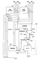
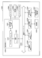
- FIG. 1 is a block diagram showing a schematic configuration example of the imaging device according to the first embodiment.
- the imaging device 100 includes an optical system 110, a solid-state imaging device 200, a recording unit 120, a control unit 130, and an external interface (I/F) 140.
- I/F external interface
- As the imaging device 100 a camera mounted on an industrial robot, a vehicle-mounted camera, or the like is assumed.
- the optical system 110 includes, for example, a lens, and forms an image of incident light on the light receiving surface of the solid-state imaging device 200.
- the solid-state imaging device 200 photoelectrically converts incident light to capture image data while detecting whether or not an address event is fired.
- the detection result indicating the presence or absence of the firing of the address event (hereinafter referred to as event detection data) and the image data of the brightness value corresponding to the incident light amount (hereinafter referred to as gradation image data) are input to the recording unit 120, for example. It may be output to the external host 150 or the like via the external I/F 140.
- the external I/F 140 is, for example, a wireless LAN (Local Area Network), a wired LAN, a communication network that conforms to any standard such as CAN (Controller Area Network), LIN (Local Interconnect Network), and FlexRay (registered trademark). It may be a communication adapter for establishing communication with the external host 150 via.
- a wireless LAN Local Area Network
- a wired LAN a communication network that conforms to any standard such as CAN (Controller Area Network), LIN (Local Interconnect Network), and FlexRay (registered trademark). It may be a communication adapter for establishing communication with the external host 150 via.
- CAN Controller Area Network
- LIN Local Interconnect Network
- FlexRay registered trademark
- the host 150 may be, for example, an ECU (Engine Control Unit) mounted in an automobile or the like when the imaging device 100 is mounted in the automobile or the like.
- an autonomous mobile robot such as a domestic pet robot, an autonomous mobile body such as a robot cleaner, an unmanned aerial vehicle, or a follow-up transport robot
- the host 150 controls the autonomous mobile body. It may be a control device or the like.
- the host 150 may be, for example, an information processing device such as a personal computer.
- the recording unit 120 is composed of, for example, a non-volatile memory such as a flash memory, and records event detection data and gradation image data input from the solid-state imaging device 200, and various other data.
- a non-volatile memory such as a flash memory
- the control unit 130 is composed of, for example, an information processing device such as a CPU (Central Processing Unit), and controls the solid-state imaging device 200 to acquire event detection data and gradation image data.
- an information processing device such as a CPU (Central Processing Unit)
- CPU Central Processing Unit
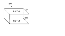
- FIG. 2 is a diagram showing a stacked structure example of the solid-state imaging device according to the first embodiment.
- the solid-state imaging device 200 has a laminated chip structure in which a light receiving chip 201 and a detection chip 202 are vertically stacked.
- a light receiving chip 201 and a detection chip 202 are vertically stacked.
- direct joining can be used, in which the respective joining surfaces are flattened and the two are attached by an electron force.
- the present invention is not limited to this, and for example, so-called Cu-Cu bonding, in which electrode pads made of copper (Cu) formed on the bonding surfaces of each other are bonded, or other bump bonding can be used. ..
- the light receiving chip 201 and the detection chip 202 are electrically connected to each other, for example, through a connecting portion such as a TSV (Through-Silicon Via) penetrating the semiconductor substrate.
- the connection using the TSV includes, for example, a so-called twin TSV method in which two TSVs, a TSV provided on the light receiving chip 201 and a TSV provided from the light receiving chip 201 to the detection chip 202, are connected on the outside of the chip, or a light receiving It is possible to employ a so-called shared TSV system or the like, in which both are connected by a TSV penetrating from the chip 201 to the detection chip 202.
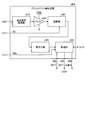
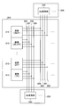
- FIG. 3 is a block diagram showing a schematic configuration example of the solid-state imaging device according to the first embodiment.
- the solid-state imaging device 200 includes a drive circuit 211, a signal processing unit 212, a Y arbiter (arbitration unit) 213, a column ADC (conversion unit) 220, an event encoder 250, and a pixel array unit. And 300.
- the pixel array unit 300 has a configuration in which a plurality of pixel blocks 310 are arranged in a two-dimensional lattice (also referred to as a matrix).
- a set of pixel blocks arranged in the horizontal direction is referred to as a “row”
- a set of pixel blocks arranged in the direction perpendicular to the rows is referred to as a “column”.
- the position in the row direction of each pixel block 310 in the pixel array unit 300 is specified by the X address, and the position in the column direction is specified by the Y address.
- Each pixel block 310 photoelectrically converts incident light to generate an analog pixel signal having a voltage value corresponding to the incident light amount. Further, the pixel block 310 detects whether or not an address event is fired based on whether or not the amount of change in the amount of incident light exceeds a predetermined threshold value.
- the pixel block 310 that detects the firing of the address event outputs a request to the Y arbiter 213.
- the pixel block 310 receives a response to the request from the Y arbiter, the pixel block 310 transmits a detection signal indicating the detection result of the address event to the drive circuit 211 and the column ADC 220.
- the Y arbiter 213 arbitrates the request from the pixel block 310 to determine the read order for the rows to which the pixel block 310 that is the request transmission source belongs, and is the request transmission source based on the determined read order. A response is returned to all the pixel blocks 310 included in the row to which the pixel block 310 belongs. In the following description, arbitrating the request to determine the reading order is referred to as “arbitrating the reading order”.
- the driving circuit 211 drives each of the pixel blocks 310 that output the detection signal, and thereby supplies a pixel signal having a voltage value corresponding to the amount of incident light to the photoelectric conversion element 321 to the vertical signal line 308 connected to each of the pixel blocks 310. Make it appear.
- the column ADC 220 reads the pixel signals in columns in parallel by converting the analog pixel signals appearing on the vertical signal lines 308 of each column into digital pixel signals for each row. Then, the column ADC 220 supplies the read digital pixel signal to the signal processing unit 212.
- the signal processing unit 212 executes predetermined signal processing such as CDS (Correlated Double Sampling) processing on the pixel signal from the column ADC 220, and outputs the gradation image data including the pixel signal after the signal processing to the outside. ..
- predetermined signal processing such as CDS (Correlated Double Sampling) processing on the pixel signal from the column ADC 220, and outputs the gradation image data including the pixel signal after the signal processing to the outside. ..
- the event encoder 250 generates, for each row in the pixel array unit 300, data indicating in which pixel block 310 an on event has occurred, and in which pixel block 310 an off event has occurred. For example, when the event encoder 250 receives a request from a certain pixel block 310, an on event or an off event has occurred in this pixel block 310, and an X address for specifying the position of the pixel block 310 in the pixel array unit 300 and Event detection data including a Y address is generated.
- the event encoder 250 also includes information (time stamp) about the time when the firing of the on event or the off event is detected in the event detection data. Then, the event encoder 250 outputs the generated event detection data to the outside.
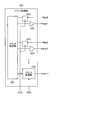
- FIG. 4 is a block diagram showing a schematic configuration example of the pixel block according to the first embodiment.
- the pixel block 310 includes a grayscale pixel 320 for generating a pixel signal which is grayscale information, an event pixel 330 for detecting whether or not an address event is fired, and an event pixel 330.
- an address event detection circuit (detection unit) 400 for detecting the presence or absence of the firing of the address event based on the photocurrent.
- FIG. 5 is a diagram showing an exemplary laminated configuration when the pixel block shown in FIG. 4 is applied to the laminated chip shown in FIG.
- the gradation pixel 320 and the event pixel 330 are arranged in the light receiving chip 201, and the address event detection circuit 400 is arranged in the detection chip 202.
- the present invention is not limited to this, and various modifications can be made, for example, by disposing a part of the circuit configuration of the gradation pixel 320 on the detection chip 202.
- FIG. 6 is a plan view showing an example of plane layout of a pixel block in the pixel array section according to the first embodiment.
- the pixel array unit 300 includes a plurality of pixel blocks 310 arranged in a matrix. Further, in the pixel array section 300, the detection signal lines 306 and 307, the vertical signal line 308, and the enable signal line 309 are wired for each column along the column direction. Each of the pixel blocks 310 is connected to the detection signal lines 306 and 307 of the corresponding column, the vertical signal line 308, and the enable signal line 309.
- FIG. 7 is a circuit diagram showing a circuit configuration example of the gradation pixel 320 according to the first embodiment.
- the grayscale pixel 320 includes a photoelectric conversion element 321, a transfer transistor 322, a floating diffusion layer 323, a reset transistor 324, an amplification transistor 325, and a selection transistor 326, and outputs a photocurrent.
- An analog signal having a corresponding voltage is generated as the pixel signal Vsig.
- the configuration other than the photoelectric conversion element 321 in the gradation pixel 320 is also referred to as a pixel circuit.
- the transfer transistor, the reset transistor 324, the amplification transistor 325, and the selection transistor 326 may be, for example, N-type MOS (Metal-Oxide-Semiconductor) transistors.
- the photoelectric conversion element (second photoelectric conversion element) 321 is composed of, for example, a photodiode, and photoelectrically converts incident light to generate electric charges.
- the transfer transistor 322 transfers charges from the photoelectric conversion element 321 to the floating diffusion layer 323 according to the transfer signal TRG from the drive circuit 211.
- the floating diffusion layer 323 is a charge storage unit that generates a voltage according to the amount of stored charges.
- the reset transistor 324 discharges (initializes) the charge of the floating diffusion layer 323 according to the reset signal RST from the drive circuit 211.
- the amplification transistor 325 amplifies the voltage of the floating diffusion layer 323.
- the selection transistor 326 causes the signal of the amplified voltage to appear on the vertical signal line 308 as the pixel signal Vsig in accordance with the selection signal SEL from the drive circuit 211.
- the pixel signal Vsig that appears on the vertical signal line 308 is read by the column ADC 220, for example, and converted into a digital pixel signal.
- FIG. 8 is a circuit diagram showing a circuit configuration example of the event pixel according to the first embodiment. As shown in FIG. 8, the event pixel 330 includes a photoelectric conversion element 331.
- the photoelectric conversion element (first photoelectric conversion element) 331 includes, for example, a photodiode, and photoelectrically converts incident light to generate electric charges.
- the charges generated by the photoelectric conversion performed by the photoelectric conversion element 331 are supplied to the address event detection circuit 400 as photocurrent.
- the address event detection circuit 400 shown in FIG. 8 depends on whether the amount of change in photocurrent flowing out from the photoelectric conversion element 331 exceeds a predetermined threshold value. , Detects the firing of address events.
- This address event includes, for example, an on event indicating that the amount of change in photocurrent according to the amount of incident light exceeds the upper limit threshold value, and an off event indicating that the amount of change is below the lower limit threshold value.
- the address event is detected when the change amount of the incident light amount is outside the predetermined range from the lower limit to the upper limit.
- the address event detection signal includes, for example, 1 bit indicating the detection result of the on event and 1 bit indicating the detection result of the off event.
- the address event detection circuit 400 can also detect only an on event.
- the address event detection circuit 400 sends a request for sending a detection signal to the Y arbiter 213 when an address event occurs. Then, when the response to the request is received from the Y arbiter 213, the address event detection circuit 400 transmits the detection signals DET+ and DET ⁇ to the drive circuit 211 and the column ADC 220.
- the detection signal DET+ is a signal indicating the detection result of the presence or absence of an on event, and is transmitted to the column ADC 220 via the detection signal line 306, for example.
- the detection signal DET- is a signal indicating the detection result of the presence or absence of an off event, and is transmitted to the column ADC 220 via the detection signal line 307, for example.
- the address event detection circuit 400 sets the column enable signal ColEN to enable in synchronization with the selection signal SEL, and transmits the signal to the column ADC 220 via the enable signal line 309.
- the column enable signal ColEN is a signal for enabling or disabling AD (Analog to Digital) conversion for the pixel signal of the corresponding column.
- the drive circuit 211 drives that row by the selection signal SEL or the like.
- Each of the pixel blocks 310 in the driven row causes the pixel signal Vsig to appear on the vertical signal line 308.
- the pixel signal Vsig appearing on the vertical signal line 308 is read by the column ADC 220 and converted into a digital pixel signal.
- the pixel block 310 that has detected the address event in the driven row transmits the column enable signal ColEN set to enable to the column ADC 220.
- the column enable signal ColEN of the pixel block 310 that has not detected the address event is set to be disabled.
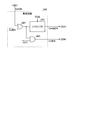
- FIG. 9 is a block diagram showing a schematic configuration example of the address event detection circuit according to the first embodiment.
- the address event detection circuit 400 includes a current/voltage conversion unit 410, a buffer 420, a subtractor 430, a quantizer 440, and a transfer unit 450.
- the current-voltage converter 410 converts the photocurrent from the event pixel 330 into a logarithmic voltage signal. Then, the current-voltage converter 410 supplies the voltage signal to the buffer 420.
- the buffer 420 outputs the voltage signal from the current-voltage converter 410 to the subtractor 430. With this buffer 420, the driving force for driving the subsequent stage can be improved. In addition, the buffer 420 can ensure the isolation of noise associated with the switching operation in the subsequent stage.
- the subtractor 430 lowers the level of the voltage signal from the buffer 420 according to the row drive signal from the drive circuit 211. Then, the subtractor 430 supplies the reduced voltage signal to the quantizer 440.
- Quantizer 440 quantizes the voltage signal from subtractor 430 into a digital signal and outputs it as a detection signal to transfer unit 450.
- the transfer unit 450 transfers the detection signal from the quantizer 440 to the signal processing unit 212 and the like.
- the transfer unit 450 transmits a request for transmitting a detection signal to the Y arbiter 213 and the event encoder 250 when an address event is detected. Then, when the transfer unit 450 receives a response to the request from the Y arbiter 213, the transfer unit 450 supplies the detection signals DET+ and DET ⁇ to the drive circuit 211 and the column ADC 220. Further, when the selection signal SEL is transmitted, the transfer unit 450 transmits the column enable signal ColEN set to enable to the column ADC 220.
- FIG. 10 is a circuit diagram showing a schematic configuration example of the current-voltage conversion unit according to the first embodiment.
- the current-voltage conversion unit 410 includes an LG (LoG) transistor 411, an amplification transistor 413, and a load MOS transistor 412.
- LG transistor 411 and the amplification transistor 413 for example, N-type MOS transistors can be used.
- the load MOS transistor 412 is a constant current circuit, and a P-type MOS transistor can be used for this.
- the source of the LG transistor 411 is connected to the cathode of the photoelectric conversion element 331 in the event pixel 330, and the drain is connected to the power supply terminal.
- the load MOS transistor 412 and the amplification transistor 413 are connected in series between the power supply terminal and the ground terminal.
- the connection point between the load MOS transistor 412 and the amplification transistor 413 is connected to the gate of the LG transistor 411 and the input terminal of the buffer 420. Further, a predetermined bias voltage Vbias is applied to the gate of the load MOS transistor 412.
- the drains of the LG transistor 411 and the amplification transistor 413 are connected to the power supply side, and such a circuit is called a source follower.
- the two source followers connected in a loop form convert the photocurrent from the photoelectric conversion element 331 into a logarithmic voltage signal.
- the load MOS transistor 412 supplies a constant current to the amplification transistor 413.
- the LG transistor 411 and the amplification transistor 413 may be arranged in the light receiving chip 201 shown in FIG.
- the source of the LG transistor 411 and the gate of the amplification transistor 413 are connected to, for example, the cathode of the photoelectric conversion element 331 in the event pixel 330.
- the drain of the LG transistor 411 is connected to, for example, the source of the LG transistor 414 and the gate of the amplification transistor 413.
- the drain of the LG transistor 414 is connected to the power supply terminal VDD, for example.
- the source of the amplification transistor 415 is connected to the gate of the LG transistor 411 and the drain of the amplification transistor 413.
- the drain of the amplification transistor 415 is connected to the power supply terminal VDD via the load MOS transistor 412, for example.
- the photocurrent from the photoelectric conversion element 331 is converted into a logarithmic voltage signal corresponding to the charge amount.
- the LG transistors 411 and 414 and the amplification transistors 413 and 415 may be configured by N-type MOS transistors, respectively.
- the LG transistors 411 and 414 and the amplification transistors 413 and 415 may be arranged in the light receiving chip 201 shown in FIG.
- FIG. 12 is a circuit diagram showing a schematic configuration example of the subtractor and the quantizer according to the first embodiment.
- the subtractor 430 includes capacitors 431 and 433, an inverter 432, and a switch 434.
- the quantizer 440 also includes comparators 441 and 442.
- One end of the capacitor 431 is connected to the output terminal of the buffer 420, and the other end is connected to the input terminal of the inverter 432.
- the capacitor 433 is connected in parallel with the inverter 432.
- the switch 434 opens and closes a path connecting both ends of the capacitor 433 in accordance with the auto-zero signal AZ from the drive circuit 211.
- the inverter 432 inverts the voltage signal input via the capacitor 431.
- the inverter 432 outputs the inverted signal to the non-inverting input terminal (+) of the comparator 441.
- (5) represents the subtraction operation of the voltage signal, and the gain of the subtraction result is C1/C2. Since it is usually desired to maximize the gain, it is preferable to design C1 to be large and C2 to be small. On the other hand, if C2 is too small, kTC noise may increase and noise characteristics may be deteriorated. Therefore, the capacity reduction of C2 is limited to a range in which noise can be allowed. Further, since the address event detection circuit 400 including the subtractor 430 is mounted for each pixel block, there is a restriction on the area of the capacitors C1 and C2. In consideration of these, the values of the capacitors C1 and C2 are determined.
- the comparator 441 compares the voltage signal from the subtractor 430 with the upper limit voltage Vbon applied to the inverting input terminal ( ⁇ ).
- the upper limit voltage Vbon is a voltage indicating an upper limit threshold.
- the comparator 441 outputs the comparison result COMP+ to the transfer unit 450.
- the comparator 441 outputs a high level comparison result COMP+ when an on event occurs, and outputs a low level comparison result COMP+ when there is no on event.
- the comparator 442 compares the voltage signal from the subtractor 430 with the lower limit voltage Vboff applied to the inverting input terminal ( ⁇ ).
- the lower limit voltage Vboff is a voltage indicating a lower limit threshold.
- the comparator 442 outputs the comparison result COMP- to the transfer unit 450.
- the comparator 442 outputs a high-level comparison result COMP- when an off event occurs, and outputs a low-level comparison result COMP- when there is no off event.
- FIG. 13 is a circuit diagram showing a schematic configuration example of the transfer unit according to the first embodiment.
- the transfer unit 450 includes AND (logical product) gates 451 and 453, an OR (logical sum) gate 452, and flip-flops 454 and 455.
- the AND gate 451 outputs the logical product of the comparison result COMP+ of the quantizer 440 and the response AckY from the Y arbiter 213 to the column ADC 220 as the detection signal DET+.
- the AND gate 451 outputs a high-level detection signal DET+ when an ON event occurs and outputs a low-level detection signal DET+ when there is no ON event.
- the OR gate 452 outputs the logical sum of the comparison result COMP+ and the comparison result COMP ⁇ of the quantizer 440 to the Y arbiter 213 as a request ReqY.
- the OR gate 452 outputs a high-level request ReqY when an address event occurs, and outputs a low-level request ReqY when there is no address event. Further, the inverted value of the request ReqY is input to the input terminal D of the flip-flop 454.
- the AND gate 453 outputs the logical product of the comparison result COMP ⁇ of the quantizer 440 and the response AckY from the Y arbiter 213 to the column ADC 220 as the detection signal DET ⁇ .
- the AND gate 453 outputs a high-level detection signal DET- when an off event occurs, and outputs a low-level detection signal DET- when there is no off event.
- the flip-flop 454 holds the inverted value of the request ReqY in synchronization with the response AckY. Then, the flip-flop 454 outputs the held value as the internal signal ColEN′ to the input terminal D of the flip-flop 455.
- the flip-flop 455 holds the internal signal ColEN' in synchronization with the selection signal SEL from the drive circuit 211. Then, the flip-flop 455 outputs the held value to the column ADC 220 as the column enable signal ColEN.
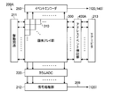
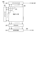
- FIG. 14 is a block diagram showing a schematic configuration example of the column ADC according to the first embodiment.
- the column ADC 220 for example, one AD conversion unit 230 is arranged for each column in the pixel array unit 300.
- the AD conversion unit 230 converts the analog pixel signal appearing on the vertical signal line 308 of each column into a digital pixel signal.
- FIG. 15 is a block diagram illustrating a schematic configuration example of the AD conversion unit according to the first embodiment.
- the AD conversion unit 230 includes an ADC 232 and a control circuit 240.
- the ADC 232 converts the pixel signal Vsig into a digital pixel signal Dout.
- the ADC 232 includes a comparator 233 and a counter 234.
- the comparator 233 compares the predetermined reference signal RMP with the pixel signal Vsig according to the comparator enable signal CompEN from the control circuit 240.
- the reference signal RMP for example, a ramp signal that changes in a slope shape or a step shape can be used.
- the comparator enable signal CompEN is a signal for enabling or disabling the comparison operation of the comparator 233.
- the comparator 233 supplies the comparison result VCO to the counter 234.
- the counter 234 According to the counter enable signal CntEN from the control circuit 240, the counter 234 counts the count value in synchronization with the clock signal CLK until the comparison result VCO is inverted.
- the counter enable signal CntEN is a signal for enabling or disabling the counting operation of the counter 234.
- the counter 234 outputs a digital pixel signal Dout indicating the count value to the signal processing unit 212.
- the control circuit 240 controls the multiplexer 231 and the ADC 232 according to the column enable signal ColEN. Details of the control contents will be described later.
- detection signals DET+ and DET ⁇ output from each pixel block 310 are output to the signal processing unit 212 via the AD conversion unit 230.
- a single-slope ADC including the comparator 233 and the counter 234 is used as the ADC 232, but the configuration is not limited to this.
- a delta-sigma type ADC can be used as the ADC 232.
- FIG. 16 is a block diagram showing a schematic configuration example of the control circuit according to the first embodiment.
- the control circuit 240 includes an OR (logical sum) gate 241, a level shifter 242, and an AND (logical product) gate 243.
- the OR gate 241 outputs a logical sum of the column enable signal ColEN and the extra enable signal ExtEN to the level shifter 242 and the AND gate 243.
- the extra enable signal ExtEN is a signal for instructing to validate AD conversion regardless of the presence or absence of an address event, and is set in accordance with a user operation or the like. For example, the high level is set to the extra enable signal ExtEN when it is enabled, and the low level is set when it is disabled.
- the level shifter 242 converts the voltage of the output signal of the OR gate 241. Then, the level shifter 242 supplies the converted signal as the comparator enable signal CompEN to the comparator 233 in the ADC 232 according to the block control signal Crtl2, for example.
- the block control signal Crtl2 is a signal for invalidating the comparator 233 regardless of the presence or absence of an address event. For example, regardless of the presence or absence of an address event, the block control signal Crtl2 is set to a low level when the comparator 233 is disabled, and is set to a high level otherwise.
- the AND gate 243 outputs the logical product of the output signal of the OR gate 241 and the block control signal Crtl1 to the counter 234 as the counter enable signal CntEN.
- the block control signal Crtl1 is a signal for invalidating the counter 234 regardless of the presence or absence of an address event. For example, regardless of the presence or absence of an address event, the block control signal Crtl1 is set to a low level when the counter 234 is invalidated, and is set to a high level otherwise.
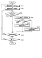
- FIG. 17 is a flowchart showing a schematic operation example of the solid-state imaging device according to the first embodiment. This operation is started, for example, when an application for detecting and imaging an address event is executed.
- the solid-state imaging device 200 starts detecting whether or not an address event has fired (step S101), and determines whether or not an address event has occurred (step S102).
- the event pixel 330 is used to detect the firing of the address event.
- the operation proceeds to step S105.
- the event encoder 250 outputs the event detection data for the pixel block 310 in which the firing of the address event is detected (step S103).
- the column ADC 220 reads out pixel signals from all the pixel blocks 310 included in the row to which the pixel block 310 in which the firing of the address event is detected belongs (step S104).
- the gradation pixel 320 is used for reading the pixel signal.
- the pixel signals for one row are read in parallel (column parallel) from all the pixel blocks 310 included in the row to which the pixel block 310 in which the firing of the address event is detected belongs. Then, the operation proceeds to step S105.
- step S105 the solid-state imaging device 200 determines whether or not to end this operation, and if it ends (YES in step S105), this operation ends. On the other hand, when the process is not completed (NO in step S105), the process returns to step S101 and the subsequent operations are executed.
- pixel signals are read in column parallel from all the pixel blocks 310 included in the row to which the pixel block 310 in which the firing of the address event is detected belongs. Be done. This makes it possible to omit the procedure of individually identifying and individually reading the pixel blocks 310 in which the address event has fired, and thus reducing the time difference from the detection of the firing of the address event to the reading of the pixel signal (gradation). It becomes possible to do.
- the circuit of the solid-state imaging device 200 can be omitted. It is also possible to simplify the configuration and reduce the size.
- a pixel for event detection (event pixel 330) and a pixel for gradation acquisition (gradation pixel 320) are provided separately, and each pixel is independently controlled. Since it is possible to eliminate the dead time from the detection of the firing of the address event to the reading of the pixel signal (gradation), it is also possible to execute the event detection and the gradation acquisition in parallel.
- a circuit other than the photoelectric conversion element 331 in the event pixel 330 is provided for one photoelectric conversion element 341.
- the configuration is connected to the circuit configuration other than the photoelectric conversion element 321 in the gradation pixel 320.
- the OFG (OverFlow Gate) transistor 332 is first turned on for the monitoring of the address event, and when the firing of the address event is detected in that state, the OFG transistor 332 is turned off.
- the transfer transistor 322 is turned on and the transfer transistor 322 is turned on, the charge generated in the photoelectric conversion element 341 is transferred to the floating diffusion layer 323 of the grayscale pixel 320. Since the pixel signal reading operation at that time is the same as the operation described above, detailed description thereof will be omitted here.
- FIG. 19 is a block diagram showing a schematic configuration example of a solid-state imaging device according to the second modified example of the first embodiment.
- 20 is a block diagram showing a schematic configuration example of a pixel block according to the second modification of the first embodiment.
- each pixel block 310 the case where the address event detection circuit 400 is provided in each pixel block 310 is illustrated, but the present invention is not limited to such a configuration, and for example, as shown in FIG. It is also possible to replace the address event detection circuit 400 of (1) with the address event detection unit 400A configured by the common address event detection circuit 400 for each row.
- the address event detection circuit 400 can be omitted from each pixel block 310A, so that the solid-state imaging device 200 can be further downsized.
- the configuration of a so-called 1-column 1-ADC in which one AD conversion unit 230 is provided for each column has been illustrated, but the configuration is not limited to such a configuration and, for example, two columns or more. It is also possible to share one AD conversion unit 230. Therefore, in the second embodiment, a case where one AD conversion unit 230 is shared by two or more columns will be described with an example.
- the configurations of the imaging device and the solid-state imaging device according to the present embodiment may be the same as, for example, the imaging device 100 and the solid-state imaging device 200 illustrated in the first embodiment.
- the AD conversion unit 230 is replaced with an AD conversion unit 530 described later.
- FIG. 21 is a block diagram showing a schematic configuration example of the AD conversion unit according to the second embodiment.
- the AD conversion unit 530 has a configuration similar to that of the AD conversion unit 230 illustrated in FIG. 15 except that the control circuit 240 is replaced by the control circuit 540 and a multiplexer 531 is added.
- the two columns corresponding to the AD conversion unit 530 are a 2m-1 (m is an integer of 1 to M) column and a 2m column.
- the multiplexer 531 selects one of the pixel signal Vsig2m-1 of the 2m-1 column and the pixel signal Vsig2m of the 2m column according to the control signal from the control circuit 540, and outputs it as the pixel signal VsigSEL to the ADC 232.
- the switch signal SW and the multiplexer enable signal MuxEN are input to the multiplexer 531 as control signals.
- the ADC 232 includes a comparator 233 and a counter 234, and converts the pixel signal VsigSEL into a digital pixel signal Dout.
- the comparator 233 compares the predetermined reference signal RMP with the pixel signal VsigSEL according to the comparator enable signal CompEN from the control circuit 540.
- the control circuit 540 controls the multiplexer 531 and the ADC 232 according to the column enable signals ColEN2m-1 and ColEN2m of the 2m-1th column and the 2mth column, respectively. Details of the control contents will be described later.
- detection signals DET+ and DET ⁇ of each column are output to the signal processing unit 212 via the AD conversion unit 530.
- a single-slope ADC including the comparator 233 and the counter 234 is used as the ADC 232, but the configuration is not limited to this.
- a delta-sigma type ADC can be used as the ADC 232.
- FIG. 22 is a block diagram showing a schematic configuration example of the control circuit 540 according to the second embodiment. As shown in FIG. 22, the control circuit 540 further includes a demultiplexer 544 and a switching control unit 545 in addition to the same configuration as the control circuit 240 illustrated in FIG. 16.
- the demultiplexer 544 distributes the output signal of the level shifter 242 to the multiplexer 531 and the comparator 233 according to the block control signal Crtl2.
- the block control signal Crtl2 is a signal for invalidating at least one of the multiplexer 531 and the comparator 233 regardless of the presence or absence of an address event.
- a binary number “10” is set to the block control signal Crtl2.
- the output signal of the level shifter 242 is output to the comparator 233 as the comparator enable signal CompEN.
- a binary number "01” is set to the block control signal Crtl2.
- the output signal of the level shifter 242 is output to the multiplexer 531 as the multiplexer enable signal MuxEN.
- both the multiplexer 531 and the comparator 233 are disabled, "00” is set, and otherwise "11” is set. When “11” is set, the output signal of the level shifter 242 is output to both the multiplexer 531 and the comparator 233.
- the switching control unit 545 switches the pixel signal output from the multiplexer 531 based on the column enable signals ColEN2m-1 and ColEN2m. For example, when the enable is set to only one side, the switching control unit 545 causes the multiplexer 531 to select the pixel signal of the enabled column by the switching signal SW. When enable is set for both of the two columns, the switching control unit 545 causes the multiplexer 531 to select the pixel signal of one column by the switching signal SW, and then selects the pixel signal of the other column.
- FIG. 23 is a diagram for explaining an example of the reading control at the time of reading the pixel signal according to the second embodiment. Note that, in the present embodiment as well, as in the first embodiment, pixel signals are read from all the pixel blocks 310 included in the row to which the pixel block 310 in which the firing of the address event is detected belongs, and therefore the pixel signals shown in FIG.
- the control is a control executed when the firing of the address event is detected in at least one pixel block 310 included in the rows to which the pixel blocks 310 in the 2m ⁇ 1th column and the 2mth column belong.
- the control circuit 540 when the firing of the address event is detected in at least one of the 2m ⁇ 1-column pixel block 310 and the 2m-column pixel block 310, the control circuit 540 outputs, for example, The multiplexer block 531 first selects the pixel block 310 of the 2m ⁇ 1th column, and then the multiplexer 531 selects the pixel block 310 of the 2mth column. At that time, the control circuit 540 enables the ADC 232 over the AD conversion periods of the 2m ⁇ 1th column and the 2mth column.
- control circuit 540 sets the ADC 232 to be disabled when both the 2m ⁇ 1th column and the 2mth column are disabled.
- FIG. 24 is a plan view showing a layout example of a part of the pixel array section and the column ADC according to the first example of the third embodiment. As shown in FIG. 24, in the pixel array section 300 according to the first example, two ADCs 232 are associated with one column.
- the pixel blocks 310 in a row are connected to the other AD conversion section 230 via different signal lines 306 to 309.
- FIG. 25 is a plan view showing a layout example of a part of the pixel array section and the column ADC according to the second example of the third embodiment. As shown in FIG. 25, in the second example, two ADCs 232 are arranged to sandwich the pixel array section 300 in the same configuration as the first example.
- the circuit scale per column ADC 220 can be reduced.
- FIG. 26 is a plan view showing a layout example of part of the pixel array section and the column ADC according to the third example of the third embodiment.
- the number of columns is 4M
- 4m columns and 4m ⁇ 2 columns are connected to the column ADC 220 arranged above the pixel array section 300, and 4m ⁇ 1 columns and 4m ⁇ 1 columns are connected.
- the 4m-3 row is connected to the column ADC 220 arranged on the lower side.
- each AD conversion unit 230 is arranged for every K columns for a total of 2M columns connected.
- K is “2”
- M AD conversion units 530 are arranged.
- the configuration of each AD conversion unit 530 according to the third example may be the same as that of the AD conversion unit 530 according to the second embodiment.
- an AD conversion unit 530 is arranged every two columns in the upper column ADC 220.
- one AD conversion unit 530 is shared by a plurality of columns, and the column ADC 220 is divided into two and arranged at positions sandwiching the pixel array unit 300. It is possible to reduce the circuit scale of the entire column ADC 220 and reduce the circuit scale of each column ADC 220.
- the configuration of the imaging device according to the present embodiment may be the same as that of the imaging device 100 illustrated in the first embodiment, for example.
- the solid-state imaging device 200 is replaced with a solid-state imaging device 600 described later.
- FIG. 27 is a block diagram showing a schematic configuration example of the solid-state imaging device according to the fourth embodiment.
- the solid-state imaging device 600 has a configuration similar to that of the solid-state imaging device 200 illustrated in FIG. 3, except that the drive circuit 211 is omitted and the Y arbiter 213 is replaced with a Y arbiter 601. ..
- the Y arbiter 601 has the same function as the Y arbiter 213 in the first embodiment, as well as the function of the drive circuit 211 in the first embodiment. Therefore, when the Y-arbiter 601 detects the firing of an address event in one or more pixel blocks 310 in the pixel array unit 300, the Y arbiter 601 arbitrates the read order for the row to which each pixel block 310 in which the firing of the address event is detected belongs. Then, each row is driven in accordance with the arbitrated read order. As a result, pixel signals are read in column parallel from each row to which the pixel block 310 in which the firing of the address event is detected belongs.
- FIG. 28 is a block diagram showing a schematic configuration example of the Y arbiter according to the fourth embodiment.
- the Y arbiter 601 includes an event processing unit 620 and a gradation pixel control unit 610.
- the event processing unit 620 When receiving the request ReqY from a plurality of pixel blocks 310 belonging to different rows, the event processing unit 620 arbitrates the reading order for the rows and returns a response AckY according to the arbitration result to all the pixel blocks 310 belonging to the row. .. On the other hand, each pixel block 310 that has received the response AckY transmits a detection signal to the column ADC 220.
- the event processing unit 620 also inputs the arbitrated read order to the gradation pixel control unit 610.
- the gradation pixel control unit 610 drives the rows according to the input read order. As a result, in all the pixel blocks 310 included in the driven row, a pixel signal having a voltage value corresponding to the amount of light incident on the photoelectric conversion element 321 appears on the vertical signal line 308.
- the column ADC 220 reads the pixel signals appearing on each vertical signal line 308 in parallel in a column to collectively read the pixel signals for one row.
- FIG. 29 is a block diagram showing a schematic configuration example of the event processing unit according to the fourth embodiment.
- the event processing unit 620 includes an address specifying unit 621, a latch circuit 622, and a driver 623.
- the latch circuit 622 is provided for each row and temporarily holds the request ReqY input from the pixel block 310. Then, the latch circuit 622 inputs the held request ReqY to the address specifying unit 621 in synchronization with the input clock CLK.
- the address identifying unit 621 identifies the Y address of the row to which the pixel block 310 that is the transmission source of the request ReqY belongs, based on the input request ReqY, and sends the response AckY to the driver 623 corresponding to the identified Y address. Output.
- the driver 623 to which the response AckY is input inputs the input response AckY to all the pixel blocks 310 included in the row corresponding to the Y address.
- FIG. 30 is a block diagram illustrating a schematic configuration example of the gray scale pixel control unit according to the fourth embodiment.
- the gradation pixel control unit 610 includes an address generation unit 611 and a driver 612.
- the address generation unit 611 specifies the Y address of the pixel block 310 that is the transmission source of the detection signal, and inputs the specified Y address to the driver 612 in synchronization with the clock CLK.
- the driver 612 appropriately inputs the reset signal RST, the transfer signal TRG, and the selection signal SEL to all the pixel blocks 310 included in the row of the Y address input from the address generation unit 611, and thus the pixels of the row Drive all blocks 310.
- the drive circuit 211 can be omitted, so that the circuit scale of the solid-state imaging device 600 can be reduced and downsized. Become.
- the configurations of the imaging device and the solid-state imaging device according to the present embodiment may be the same as, for example, the imaging device 100 and the solid-state imaging device 200, 200A, or 600 illustrated in the above-described embodiments.
- the base embodiment is not limited to the fourth embodiment, and other embodiments can be used.
- the solid-state imaging device 200 performs an address event detection operation of asynchronously detecting the firing of an address event, and a cycle of periodically acquiring gradation image data from the pixel block 310. Read operation is performed.
- FIG. 31 is a flowchart showing an example of the event detection operation according to the fifth embodiment. This operation is started, for example, when an application for detecting and imaging an address event is executed.
- the solid-state imaging device 200 starts detecting whether or not an address event is fired (step S701), and determines whether or not an address event has occurred (step S702).
- the event pixel 330 is used to detect the firing of the address event.
- the operation proceeds to step S704.
- step S703 when the firing of the address event is detected (YES in step S702), the event encoder 250 outputs the event detection data for the pixel block 310 in which the firing of the address event is detected (step S703), and then The operation proceeds to step S704.
- the event detection data read in step S703 is stored in the recording unit 120 or transmitted to the host 150 via the external I/F 140.
- step S704 the solid-state imaging device 200 determines whether or not to end this operation, and if it ends (YES in step S704), this operation is ended. On the other hand, when the process is not completed (NO in step S704), the process returns to step S701 and the subsequent operations are executed.
- FIG. 32 is a flowchart showing an example of the periodic read operation according to the fifth embodiment. Similar to the event detection operation, this operation is started, for example, when an application for detecting and imaging an address event is executed.
- the solid-state imaging device 200 starts measuring elapsed time (step S721) and waits until a predetermined time has elapsed (NO in step S722). After that, when a predetermined time has elapsed (YES in step S722), the solid-state imaging device 200 causes the gradation pixel control unit 610 of the Y arbiter 601 to execute the reading of pixel signals from all the pixel blocks 310 (step S723), and Proceed to S724.
- the pixel signal read in step S723 is stored in the recording unit 120 as gradation image data or is transmitted to the host 150 via the external I/F 140.
- step S724 the solid-state imaging device 200 determines whether or not to end this operation, and if it ends (YES in step S724), this operation is ended. On the other hand, if not completed (NO in step S724), the counter or the like that measures the elapsed time is reset (step S725), and then the process returns to step S722 to execute the subsequent operations.
- the gradation image data read by the periodic read operation is sequentially updated using the event detection data output by the event detection operation (gradation image data update operation).
- This gradation image data updating operation may be executed by, for example, the signal processing unit 212 in the solid-state imaging device 200, or may be executed by the external control unit 130, the host 150, or the like.
- FIG. 33 is a flowchart showing an example of the gradation image data updating operation according to the fifth embodiment. In this description, an example will be given in which the host 150 executes the gradation image data updating operation.
- step S301 when the host 150 receives the gradation image data from the solid-state imaging device 200 (step S301), the host 150 stores the input gradation image data in a predetermined memory (step S302).
- step S303 the host 150 determines whether or not the event detection data is input from the solid-state imaging device 200 within a predetermined time (step S303), and if not input (NO in step S303), the process proceeds to step S308.
- step S303 when the event detection data is input (YES in step S303), the host 150 accumulates the input event detection data in a predetermined memory (step S304).
- the host 150 determines whether the input event detection data indicates an on event or an off event (step S305), and if the input event detection data indicates an on event (YES in step S305), the event detection data
- the gradation value of the pixel is increased by adding a predetermined value to the gradation value (also referred to as a pixel value) of the pixel specified by the X address and the Y address included in step S306, and the process proceeds to step S308. move on.
- step S305 the host 150 determines the pixel specified by the X address and the Y address included in the event detection data. By subtracting a predetermined value from the gradation value (also referred to as a pixel value) of (3), the gradation value of the pixel is reduced (step S307), and the process proceeds to step S308.
- step S308 it is determined whether or not a predetermined time has elapsed since the input of the previous gradation image data. If the predetermined time has not elapsed (NO in step S308), the host 150 returns to step S303. , Execute the following operations. On the other hand, if the predetermined time has elapsed (YES in step S308), the host 150 determines whether or not to end this operation (step S309), and if it ends (YES in step S309), this operation is performed. finish. On the other hand, if not completed (NO in step S309), the host 150 returns to step S301, inputs the next gradation image data, and executes the subsequent operations.
- the predetermined time may be the acquisition cycle of the gradation image data in the solid-state imaging device 200, that is, the frame rate.
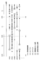
- FIG. 34 is a timing chart showing an operation example of the solid-state imaging device according to the fifth embodiment. Note that FIG. 34 shows an operation example of the pixel block 310 in a certain column. In addition, FIG. 35 is a timing chart for explaining the update of the gradation value focusing on the pixel block on the second row in FIG. 34.
- the reset operation and the pixels for the gradation pixels 320 are sequentially performed in order from the pixel block 310 in the first row in synchronization with the frame synchronization signal XVS input in a predetermined cycle T1.
- a signal read operation is executed.
- the presence or absence of the firing of an address event using the event pixel 330 is detected asynchronously.
- the gradation value by the pixel signal read from the gradation pixel 320 at the timing t1 is the next timing t2.
- the detected address event is an on event each time an address event is detected by the event pixel 330 until the pixel signal is read from the grayscale pixel 320 at, that is, during the period from timing t1 to t2.
- the value is increased or decreased by a predetermined value depending on whether it is an off event.
- the gradation value by the pixel signal read from the gradation pixel 320 at the timing t2 is the address event at the event pixel 330 during the period from the timing t2 to t3.
- Each time is detected, it is increased or decreased by a predetermined value depending on whether the detected address event is an on event or an off event.
- the pixel signals are periodically read from all or some of the pixel blocks 310 regardless of the firing of the address event, and the grayscale image data read by this is read.
- the case where the event detection data is updated is illustrated.
- the gradation value due to the pixel signal read from the gradation pixel 320 has not changed.
- the pixels from the grayscale pixel 320 are selected.
- the case where no signal is read will be described with an example.
- the configurations of the imaging device and the solid-state imaging device according to the present embodiment are similar to those of the fifth embodiment, for example, the imaging device 100 and the solid-state imaging device 200, 200A, or 600 illustrated in the above-described embodiments. Good.
- the event processing unit 620 illustrated in FIG. 29 is replaced with the event processing unit 720 described later. Note that, in the following description, the case where the fourth embodiment is used as a base is illustrated, but the base embodiment is not limited to the fourth embodiment, and other embodiments are possible.
- FIG. 36 is a block diagram showing a schematic configuration example of the event processing unit according to the sixth embodiment.
- the event processing unit 720 further includes an address storage unit 721 in addition to the same configuration as the event processing unit 620 illustrated in FIG.
- the address specifying unit 621 specifies the X address and the Y address of the pixel block 310 that is the transmission source of the request ReqY based on the input request ReqY, and corresponds to the specified X address and Y address.
- the response AckY is output to the driver 623 that operates.
- the driver 623 to which the response AckY is input inputs the input response AckY to the pixel block 310 specified by the X address and the Y address.
- the address storage unit 721 also temporarily holds the X address and the Y address (address information) specified by the address specifying unit 621. After that, the address storage unit 721 inputs the held X address and Y address to the address generation unit 611 of the gradation pixel control unit 610 in synchronization with the frame synchronization signal XVS.
- the address generation unit 611 of the gradation pixel control unit 610 inputs the X address and Y address input from the address storage unit 721 to the driver 612 in synchronization with the clock CLS. Then, the driver 612 appropriately inputs the reset signal RST, the transfer signal TRG, and the selection signal SEL to the pixel block 310 specified by the X address and the Y address input from the address generation unit 611, and thereby the pixel concerned. Drive block 310.
- FIG. 37 is a timing chart showing an example of operation of the solid-state imaging device according to the sixth embodiment. Note that, similar to FIG. 34, FIG. 37 illustrates an operation example of the pixel block 310 in a certain column.
- the operation of resetting the gradation pixel 320 is performed in the period of the next cycle T1.
- the pixel signal read operation is not executed.
- the firing of the address event is detected once or more during the period from timing t10 to t11, so that in the next cycle (timing t12 to t13), the second row
- the reset operation and the read operation for the grayscale pixels 320 of the pixel block 310 are being executed.
- the configurations of the imaging device and the solid-state imaging device according to the present embodiment are similar to those of the fifth embodiment, for example, the imaging device 100 and the solid-state imaging device 200, 200A, or 600 illustrated in the above-described embodiments. Good. However, in the present embodiment, the pixel block 310 illustrated in FIG. 4 is replaced with a pixel block 810 described later. Note that, in the following description, the case where the fourth embodiment is used as a base is illustrated, but the base embodiment is not limited to the fourth embodiment, and other embodiments are possible.
- FIG. 38 is a block diagram showing a schematic configuration example of a pixel block according to the seventh embodiment.
- the gradation pixel 320 further includes a memory 801.
- the memory 801 is a charge storage unit that temporarily holds the charges generated in the photoelectric conversion element 321, and may be configured using, for example, a capacitive element formed on the same semiconductor substrate as the photoelectric conversion element 321.
- Electric charges generated in the photoelectric conversion element 321 according to the amount of incident light are temporarily transferred to and retained in the memory 801. After that, the charge held in the memory 801 is transferred to the floating diffusion layer 323 by the read operation for the gradation pixel 320, and thereafter, the same operation as the normal read operation is executed.
- FIG. 39 is a timing chart showing an example of the pixel signal read operation according to the seventh embodiment. Note that FIG. 39 shows an operation example of the pixel block 810 in a certain column.
- charges are transferred from the photoelectric conversion element 321 in the gradation pixel 320 of each pixel block 810 to the memory 801 in synchronization with the frame synchronization signal XVS. After that, for example, the pixel signal reading operation is sequentially performed from the pixel block 810 in the first row to the pixel block 810 in the last row.
- event detection operation may be the same as in the above-described embodiment.
- the charge generated in the photoelectric conversion element 321 of the grayscale pixel 320 is temporarily held in the memory 801 so that the shutter operation (reset operation) of all the pixel blocks 810 is performed. It is possible to realize a so-called global shutter operation in which (equivalent) is simultaneously executed.
- the gradation pixel 320 Due to the progress of process technology in recent years, the gradation pixel 320 is becoming finer. Therefore, in the case where the gradation pixel 320 and the event pixel 330 are combined as in the above-described embodiment, the gradation pixel 320 and the address event detection circuit for detecting the presence or absence of the firing of the address event from the event pixel 330. The difference in pitch (or size) from 400 becomes large.
- the same area as the address event detection circuit 400 is provided in the area on the light receiving chip 201 having the same size as the area of one address event detection circuit 400.
- Gradation pixels 320 and event pixels 330 belonging to the pixel block 310 may be arranged.
- gradation pixel 320 it is conceivable to add the gradation pixel 320 to the surplus area on the light receiving chip 201 caused by the size difference between the gradation pixel 320 and the address event detection circuit 400. In that case, a plurality of gradation pixels 320 belong to one pixel block 310.
- a structured light method For example, in a distance measurement method using a structured light (hereinafter referred to as a structured light method), it is necessary to improve the positional accuracy of each dot by making the event pixel 330 fine to obtain the center of gravity of the dot. There is.
- the dots of the structured light to be irradiated include on/off codes in the time direction, that is, each dot is blinked in a different pattern, so that the structured pattern is generated from the address event generation pattern in the event pixel 330. It is possible to specify which dot in the light, and it is possible to greatly simplify the signal processing in distance measurement.
- a plurality of event pixels 330 are scattered and arranged in one pixel block, and the sum of the currents thereof is received by one address event detection circuit 400, whereby the sensitivity to the firing of the address event is improved.
- the configuration of the pixel block that enables the center of gravity of the dots of the structured light to be acquired accurately without dropping will be described with an example.
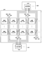
- FIG. 41 is a schematic diagram showing a schematic configuration example of a pixel block according to the eighth embodiment.
- the white squares in the light receiving chip 201 indicate the gradation pixels 320
- the hatched squares indicate the event pixels 330.
- the pixel block 910 includes one address event detection circuit 400, four event pixels 330, and 32 gradation pixels 320.
- a total of 36 pixels including event pixels 330 and gradation pixels 320 are arranged in a 6 ⁇ 6 matrix.
- the 6 ⁇ 6 matrix pixel array 911 is The area is a 6 ⁇ m square area.
- the size of the address event detection circuit 400 in the detection chip 202 may be a rectangular area of 6 ⁇ m square.
- the event pixels 330 are scattered at equal intervals (for example, every two pixels are arranged in the vertical direction and the horizontal direction). As described above, by scattering the event pixels 330 at equal intervals, it is possible to accurately obtain the barycenter of the dots of the structured light.
- the four event pixels 330 of the same pixel block 910 are connected to the same address event detection circuit 400.
- the address event detection circuit 400 receives the sum of currents from a plurality (four in this example) of the event pixels 330, so that the center of gravity of the dots of the structured light can be accurately measured without lowering the sensitivity to the firing of the address event. It becomes possible to ask well.
- the size of the light receiving area of the event pixel 330 included in one pixel block 1010 may be increased.
- the size of the light receiving area of one event pixel 330 may be the same as the size of the light receiving area of 2 ⁇ 2 gradation pixels 320. .. In that case, the event pixels 330 are arranged using the 2 ⁇ 2 pixel area in the 6 ⁇ 6 pixel array 1011.
- the size of the light receiving area of each event pixel 330 may be increased as illustrated in FIG.
- the technology according to the present disclosure (this technology) can be applied to various products.
- the technology according to the present disclosure is realized as a device mounted on any type of moving body such as an automobile, an electric vehicle, a hybrid electric vehicle, a motorcycle, a bicycle, personal mobility, an airplane, a drone, a ship, and a robot. May be.
- FIG. 43 is a block diagram showing a schematic configuration example of a vehicle control system which is an example of a mobile body control system to which the technology according to the present disclosure can be applied.
- the vehicle control system 12000 includes a plurality of electronic control units connected via a communication network 12001.
- the vehicle control system 12000 includes a drive system control unit 12010, a body system control unit 12020, a vehicle exterior information detection unit 12030, a vehicle interior information detection unit 12040, and an integrated control unit 12050.
- a microcomputer 12051, a voice image output unit 12052, and an in-vehicle network I/F (interface) 12053 are shown as a functional configuration of the integrated control unit 12050.
- the drive system control unit 12010 controls the operation of devices related to the drive system of the vehicle according to various programs.
- the drive system control unit 12010 includes a drive force generation device for generating a drive force of a vehicle such as an internal combustion engine or a drive motor, a drive force transmission mechanism for transmitting the drive force to wheels, and a steering angle of the vehicle. It functions as a steering mechanism for adjusting and a control device such as a braking device for generating a braking force of the vehicle.
- the body system control unit 12020 controls the operation of various devices mounted on the vehicle body according to various programs.
- the body system control unit 12020 functions as a keyless entry system, a smart key system, a power window device, or a control device for various lamps such as a head lamp, a back lamp, a brake lamp, a winker, or a fog lamp.
- the body system control unit 12020 may receive radio waves or signals of various switches transmitted from a portable device that substitutes for a key.
- the body system control unit 12020 receives these radio waves or signals and controls the vehicle door lock device, power window device, lamp, and the like.
- the vehicle exterior information detection unit 12030 detects information outside the vehicle equipped with the vehicle control system 12000.
- the image pickup unit 12031 is connected to the vehicle exterior information detection unit 12030.
- the vehicle exterior information detection unit 12030 causes the image capturing unit 12031 to capture an image of the vehicle exterior and receives the captured image.
- the vehicle exterior information detection unit 12030 may perform object detection processing or distance detection processing such as people, vehicles, obstacles, signs, or characters on the road surface based on the received image.
- the image pickup unit 12031 is an optical sensor that receives light and outputs an electric signal according to the amount of received light.
- the imaging unit 12031 can output the electric signal as an image or can output the information as distance measurement information.
- the light received by the imaging unit 12031 may be visible light or invisible light such as infrared light.
- the in-vehicle information detection unit 12040 detects in-vehicle information.
- a driver state detection unit 12041 that detects the state of the driver is connected.
- the driver state detection unit 12041 includes, for example, a camera that captures an image of the driver, and the in-vehicle information detection unit 12040 determines the degree of tiredness or concentration of the driver based on the detection information input from the driver state detection unit 12041. It may be calculated or it may be determined whether or not the driver is asleep.
- the microcomputer 12051 calculates the control target value of the driving force generation device, the steering mechanism or the braking device based on the information on the inside and outside of the vehicle acquired by the outside information detection unit 12030 or the inside information detection unit 12040, and the drive system control unit.
- a control command can be output to 12010.
- the microcomputer 12051 realizes functions of ADAS (Advanced Driver Assistance System) including avoidance or impact mitigation of vehicle, follow-up traveling based on inter-vehicle distance, vehicle speed maintenance traveling, vehicle collision warning, vehicle lane departure warning, etc. It is possible to perform cooperative control for the purpose.
- ADAS Advanced Driver Assistance System
- the microcomputer 12051 controls the driving force generation device, the steering mechanism, the braking device, or the like based on the information around the vehicle acquired by the vehicle exterior information detection unit 12030 or the vehicle interior information detection unit 12040, thereby It is possible to perform cooperative control for the purpose of autonomous driving or the like that autonomously travels without depending on the operation.
- the microcomputer 12051 can output a control command to the body system control unit 12020 based on the information outside the vehicle acquired by the outside information detection unit 12030.
- the microcomputer 12051 controls the headlamp according to the position of the preceding vehicle or the oncoming vehicle detected by the vehicle exterior information detection unit 12030, and performs cooperative control for the purpose of anti-glare such as switching the high beam to the low beam. It can be carried out.
- the voice image output unit 12052 transmits an output signal of at least one of a voice and an image to an output device capable of visually or audibly notifying information to a passenger of the vehicle or the outside of the vehicle.
- an audio speaker 12061, a display unit 12062, and an instrument panel 12063 are illustrated as output devices.
- the display unit 12062 may include, for example, at least one of an onboard display and a head-up display.
- FIG. 44 is a diagram showing an example of the installation position of the imaging unit 12031.
- the image pickup unit 12031 includes image pickup units 12101, 12102, 12103, 12104, and 12105.
- the imaging units 12101, 12102, 12103, 12104, 12105 are provided at positions such as the front nose of the vehicle 12100, the side mirrors, the rear bumper, the back door, and the upper part of the windshield inside the vehicle.
- the image capturing unit 12101 provided on the front nose and the image capturing unit 12105 provided on the upper part of the windshield in the vehicle interior mainly acquire an image in front of the vehicle 12100.
- the imaging units 12102 and 12103 included in the side mirrors mainly acquire images of the side of the vehicle 12100.
- the image capturing unit 12104 provided on the rear bumper or the back door mainly acquires an image of the rear of the vehicle 12100.
- the imaging unit 12105 provided on the upper part of the windshield in the vehicle interior is mainly used for detecting a preceding vehicle, a pedestrian, an obstacle, a traffic signal, a traffic sign, a lane, or the like.
- FIG. 44 shows an example of the shooting range of the imaging units 12101 to 12104.
- the imaging range 12111 indicates the imaging range of the imaging unit 12101 provided on the front nose
- the imaging ranges 12112 and 12113 indicate the imaging ranges of the imaging units 12102 and 12103 provided on the side mirrors
- the imaging range 12114 indicates The imaging range of the imaging part 12104 provided in a rear bumper or a back door is shown. For example, by overlaying the image data captured by the image capturing units 12101 to 12104, a bird's-eye view image of the vehicle 12100 viewed from above can be obtained.
- At least one of the imaging units 12101 to 12104 may have a function of acquiring distance information.
- at least one of the image capturing units 12101 to 12104 may be a stereo camera including a plurality of image capturing elements, or may be an image capturing element having pixels for phase difference detection.
- the microcomputer 12051 based on the distance information obtained from the imaging units 12101 to 12104, the distance to each three-dimensional object within the imaging range 12111 to 12114 and the temporal change of this distance (relative speed with respect to the vehicle 12100). By determining, the closest three-dimensional object on the traveling path of the vehicle 12100, which is traveling in the substantially same direction as the vehicle 12100 at a predetermined speed (for example, 0 km/h or more), can be extracted as the preceding vehicle. it can. Further, the microcomputer 12051 can set an inter-vehicle distance to be secured in advance before the preceding vehicle, and can perform automatic brake control (including follow-up stop control), automatic acceleration control (including follow-up start control), and the like. In this way, it is possible to perform cooperative control for the purpose of autonomous driving or the like that autonomously travels without depending on the operation of the driver.
- automatic brake control including follow-up stop control
- automatic acceleration control including follow-up start control
- the microcomputer 12051 uses the distance information obtained from the image capturing units 12101 to 12104 to convert three-dimensional object data regarding a three-dimensional object into another three-dimensional object such as a two-wheeled vehicle, an ordinary vehicle, a large vehicle, a pedestrian, and a utility pole. It can be classified and extracted and used for automatic avoidance of obstacles. For example, the microcomputer 12051 distinguishes obstacles around the vehicle 12100 into obstacles visible to the driver of the vehicle 12100 and obstacles difficult to see. Then, the microcomputer 12051 determines the collision risk indicating the risk of collision with each obstacle, and when the collision risk is equal to or more than the set value and there is a possibility of collision, the microcomputer 12051 outputs the audio through the audio speaker 12061 and the display unit 12062. A driver can be assisted for collision avoidance by outputting an alarm to the driver and performing forced deceleration or avoidance steering via the drive system control unit 12010.
- At least one of the imaging units 12101 to 12104 may be an infrared camera that detects infrared rays.
- the microcomputer 12051 can recognize the pedestrian by determining whether or not the pedestrian is present in the images captured by the imaging units 12101 to 12104.
- a procedure of extracting a feature point in an image captured by the image capturing units 12101 to 12104 as an infrared camera and a pattern matching process on a series of feature points indicating the contour of an object are performed to determine whether the pedestrian is a pedestrian. It is performed by the procedure of determining.
- the audio image output unit 12052 causes the recognized pedestrian to have a rectangular contour line for emphasis.
- the display unit 12062 is controlled so as to superimpose and display.
- the audio image output unit 12052 may control the display unit 12062 to display an icon indicating a pedestrian or the like at a desired position.
- the technology according to the present disclosure can be applied to, for example, the imaging unit 12031 among the configurations described above.
- the imaging device 100 of FIG. 1 can be applied to the imaging unit 12031.
- the power consumption of the image capturing unit 12031 can be reduced, and thus the power consumption of the entire vehicle control system can be reduced.
- the processing procedure described in the above-described embodiment may be regarded as a method having these series of procedures, or as a program for causing a computer to execute the series of procedures or a recording medium storing the program. May be.
- this recording medium for example, a CD (Compact Disc), an MD (MiniDisc), a DVD (Digital Versatile Disc), a memory card, a Blu-ray disc (Blu-ray (registered trademark) Disc), or the like can be used.
- a pixel array section including a plurality of pixel blocks arranged in a matrix;
- a detection unit that detects the firing of the address event based on the charge generated in the first photoelectric conversion element;
- a second photoelectric conversion element that generates an electric charge according to the amount of incident light;
- a solid-state imaging device comprising: (2) The solid-state imaging device according to (1), wherein the drive circuit causes each of the plurality of second pixel blocks included in the row to which the first pixel block belongs to generate a pixel signal.
- the solid-state imaging device further including a conversion unit that reads in parallel the pixel signals generated by each of the plurality of second pixel blocks.
- a conversion unit that reads in parallel the pixel signals generated by each of the plurality of second pixel blocks.
- the read order for each of the rows to which the one or more first pixel blocks belong is determined.
- the solid-state imaging device according to (2) or (3), further including an arbitration unit for determining.
- the first pixel block outputs, to the arbitration unit, a request for arbitrating the read order for the row to which the first pixel block belongs
- the arbitration unit is provided in a one-to-one relationship with each row, and includes a plurality of latch circuits for temporarily holding the requests input from the corresponding rows, Each of the latch circuits inputs the held request to the arbitration unit in synchronization with a clock input from the outside,
- the solid-state imaging device according to (4) or (5), wherein the arbitration unit determines the reading order based on the request input via the latch circuit.
- the drive circuit causes at least one third pixel block of the plurality of pixel blocks to generate the pixel signal at a predetermined cycle.
- the arbitration unit includes an address storage unit that stores address information that identifies a position in the pixel array unit of the first pixel block that has detected the address event within a predetermined period, The drive circuit generates the pixel signal at the predetermined cycle by using the first pixel block specified by the address information stored in the address storage unit as the third pixel block.
- Each of the pixel blocks further includes a memory that temporarily holds charges generated in the second photoelectric conversion element, When the first pixel block detects the firing of the address event, the drive circuit sends a pixel signal to the first pixel block based on the electric charge held in the memory of the first pixel block. Generate the solid-state imaging device according to (1).
- the arbitration unit includes an address storage unit that stores address information that identifies a position in the pixel array unit of the first pixel block that has detected the address event within a predetermined period,
- the solid-state imaging device according to (10), wherein the drive circuit causes the first pixel block identified by the address information stored in the address storage unit to generate a pixel signal at a predetermined cycle.
- Each of the pixel blocks includes a plurality of the first photoelectric conversion elements, The solid-state imaging device according to any one of (1) to (11), wherein the plurality of first photoelectric conversion elements are connected to the detection unit. (13) Each of the pixel blocks further includes a plurality of the second photoelectric conversion elements, The plurality of first photoelectric conversion elements and the plurality of second photoelectric conversion elements form a matrix array, The solid-state imaging device according to (12), wherein the plurality of first photoelectric conversion elements are scattered at equal intervals in the matrix arrangement. (14) The solid-state imaging device according to any one of (1) to (13), wherein the size of the light receiving area of the first photoelectric conversion element is larger than the size of the light receiving area of the second photoelectric conversion element.
- a solid-state imaging device An optical system for forming an image of incident light on the light receiving surface of the solid-state imaging device, A recording unit that stores image data acquired by the solid-state imaging device, Equipped with The solid-state imaging device, A pixel array section including a plurality of pixel blocks arranged in a matrix; A driving circuit for generating a pixel signal in a first pixel block in which the firing of an address event is detected among the plurality of pixel blocks; Equipped with Each of the pixel blocks is A first photoelectric conversion element that generates an electric charge according to the amount of incident light; A detection unit that detects the firing of the address event based on the charge generated in the first photoelectric conversion element; A second photoelectric conversion element that generates an electric charge according to the amount of incident light; A pixel circuit for generating a pixel signal based on charges generated in the second photoelectric conversion element; An imaging device including.
- Imaging Device 110 Optical System 120 Recording Unit 130 Control Unit 140 External I/F 150 Host 200, 200A, 600 Solid-state imaging device 201 Light receiving chip 202 Detection chip 211 Drive circuit 212 Signal processing unit 213, 601 Y arbiter 220 Column ADC 230, 530 AD conversion section 233 Comparator 234 Counter 240, 540 Control circuit 241 OR gate 242 Level shifter 243 AND gate 250 Event encoder 300 Pixel array section 306, 307 Detection signal line 308 Vertical signal line 309 Enable signal line 310, 310A, 810 , 910, 1010 Pixel block 320 Gray scale pixel 321, 331, 341 Photoelectric conversion element 322 Transfer transistor 323 Floating diffusion layer 324 Reset transistor 325 Amplification transistor 326 Select transistor 330 Event pixel 332 OFG transistor 400 Address event detection circuit 400A Address event detection unit 410, 410A Current-voltage converter 411, 414 LG transistor 412 Load MOS transistor 413, 415 Amplification transistor 420 Buffer 430 Sub
Landscapes
- Engineering & Computer Science (AREA)
- Multimedia (AREA)
- Signal Processing (AREA)
- Transforming Light Signals Into Electric Signals (AREA)
Abstract
イベント検出と階調取得との時間的なずれを低減する。実施形態に係る固体撮像装置は、行列状に配列する複数の画素ブロック(310)を備える画素アレイ部(300)と、前記複数の画素ブロックのうち、アドレスイベントの発火が検出された第1画素ブロックに画素信号を生成させる駆動回路(211)とを備え、前記画素ブロックそれぞれは、入射光量に応じた電荷を発生させる第1光電変換素子(331)と、前記第1光電変換素子に発生した電荷に基づいて前記アドレスイベントの発火を検出する検出部(400)と、入射光量に応じた電荷を発生させる第2光電変換素子(321)と、前記第2光電変換素子に発生した電荷に基づく画素信号を生成する画素回路(322、323、324、325、326)とを備える。
Description
本開示は、固体撮像装置及び撮像装置に関する。
従来より、垂直同期信号などの同期信号に同期して画像データ(フレーム)を撮像する同期型の固体撮像装置が、撮像装置などにおいて用いられている。この一般的な同期型の固体撮像装置では、同期信号の周期(例えば、1/60秒)ごとにしか画像データを取得することができないため、交通やロボットなどに関する分野において、より高速な処理が要求された場合に対応することが困難になる。そこで、受光量が閾値を超えたことをアドレスイベントとしてリアルタイムに検出する検出回路を画素毎に設けた非同期型の固体撮像装置が提案されている。画素毎にアドレスイベントを検出する非同期型の固体撮像装置は、DVS(Dynamic Vision Sensor)とも称される。
また、近年では、アドレスイベントの検出と合せて階調画像を取得するDVSも開発されてきている。
アドレスイベントの検出と合せて階調画像を取得するDVSとしては、画素毎ではなく画素ブロック毎に検出回路を配置し、画素ブロック単位でイベントを検出しつつ、1画素単位で階調取得を行う方法が提案されている。しかしながら、このような方法では、同一の画素を用いてイベント検出と階調取得との両方を時分割で行なう必要があるため、変化が高速なシーン等では、イベント検出と階調取得との時間的なずれから、撮影したい被写体の階調画像を取得することができないという可能性が存在する。
そこで本開示では、イベント検出と階調取得との時間的なずれを低減することが可能な固体撮像装置及び撮像装置を提案する。
上記の課題を解決するために、本開示に係る一形態の固体撮像装置は、行列状に配列する複数の画素ブロックを備える画素アレイ部と、前記複数の画素ブロックのうち、アドレスイベントの発火が検出された第1画素ブロックに画素信号を生成させる駆動回路とを備え、前記画素ブロックそれぞれは、入射光量に応じた電荷を発生させる第1光電変換素子と、前記第1光電変換素子に発生した電荷に基づいて前記アドレスイベントの発火を検出する検出部と、入射光量に応じた電荷を発生させる第2光電変換素子と、前記第2光電変換素子に発生した電荷に基づく画素信号を生成する画素回路とを備える。
以下に、本開示の一実施形態について図面に基づいて詳細に説明する。なお、以下の実施形態において、同一の部位には同一の符号を付することにより重複する説明を省略する。
また、以下に示す項目順序に従って本開示を説明する。
1.第1の実施形態
1.1 撮像装置の構成例
1.2 固体撮像装置の積層構成例
1.3 固体撮像装置の概略構成例
1.4 画素ブロックの構成例
1.4.1 画素ブロックの積層構成例
1.4.2 画素アレイ部における画素ブロックの平面レイアウト例
1.4.3 階調画素の回路構成例
1.4.4 イベント画素の回路構成例
1.4.5 アドレスイベント検出回路の機能例
1.4.6 アドレスイベント検出回路の構成例
1.4.6.1 電流電圧変換部の構成例
1.4.6.1.1 電流電圧変換部の変形例
1.4.7 減算器及び量子化器の構成例
1.4.8 転送部の構成例
1.4.9 カラムADCの構成例
1.4.9.1 AD変換部の構成例
1.4.9.2 制御回路の構成例
1.5 固体撮像装置の動作例
1.6 作用・効果
1.7 第1変形例
1.8 第2変形例
2.第2の実施形態
2.1 AD変換部の構成例
2.2 制御回路の構成例
2.3 画素信号読出し時の切替制御例
2.4 作用・効果
3.第3の実施形態
3.1 第1例
3.2 第2例
3.3 第3例
4.第4の実施形態
4.1 固体撮像装置の概略構成例
4.2 Yアービタの概略構成例
4.3 イベント処理部の概略構成例
4.4 階調画素制御部の概略構成例
4.5 作用・効果
5.第5の実施形態
5.1 固体撮像装置の動作例
5.1.1 イベント検出動作例
5.1.2 周期的読出し動作例
5.2 階調画像データ更新動作例
5.2.1 フローチャート
5.2.2 タイミングチャート
5.3 作用・効果
6.第6の実施形態
6.1 イベント処理部の概略構成例
6.2 階調画像データ更新動作例
6.3 作用・効果
7.第7の実施形態
7.1 画素ブロックの構成例
7.2 画素信号読出し動作例
7.3 作用・効果
7.4 変形例
8.第8の実施形態
8.1 変形例
9.移動体への応用例
1.第1の実施形態
まず、第1の実施形態について、図面を参照して詳細に説明する。
まず、第1の実施形態について、図面を参照して詳細に説明する。
1.1 撮像装置の構成例
図1は、第1の実施形態に係る撮像装置の概略構成例を示すブロック図である。図1に示すように、撮像装置100は、光学系110と、固体撮像装置200と、記録部120と、制御部130と、外部インタフェース(I/F)140とを備える。撮像装置100としては、産業用ロボットに搭載されるカメラや、車載カメラなどが想定される。
図1は、第1の実施形態に係る撮像装置の概略構成例を示すブロック図である。図1に示すように、撮像装置100は、光学系110と、固体撮像装置200と、記録部120と、制御部130と、外部インタフェース(I/F)140とを備える。撮像装置100としては、産業用ロボットに搭載されるカメラや、車載カメラなどが想定される。
光学系110は、例えば、レンズ等を含み、入射光の像を固体撮像装置200の受光面に結像させる。
固体撮像装置200は、アドレスイベントの発火の有無を検出しつつ、入射光を光電変換して画像データを撮像する。アドレスイベントの発火の有無を示す検出結果(以下、イベント検出データという)と、入射光量に応じた輝度値の画像データ(以下、階調画像データという)とは、例えば、記録部120に入力されてもよいし、外部I/F140を介して外部のホスト150等へ出力されてもよい。
外部I/F140は、例えば、無線LAN(Local Area Network)や有線LANの他、CAN(Controller Area Network)、LIN(Local Interconnect Network)、FlexRay(登録商標)等の任意の規格に準拠した通信ネットワークを介して外部のホスト150と通信を確立するための通信アダプタであってよい。
ここで、ホスト150は、例えば、撮像装置100が自動車等に実装される場合には、自動車等に搭載されているECU(Engine Control Unit)などであってよい。また、撮像装置100が家庭内ペットロボットなどの自律移動ロボットやロボット掃除機や無人航空機や追従運搬ロボットなどの自律移動体に搭載されている場合には、ホスト150は、その自律移動体を制御する制御装置等であってよい。その他、ホスト150は、例えば、パーソナルコンピュータなどの情報処理装置であってもよい。
記録部120は、例えば、フラッシュメモリなどの不揮発性メモリ等で構成され、固体撮像装置200から入力されたイベント検出データ及び階調画像データやその他各種データを記録する。
制御部130は、例えば、CPU(Central Processing Unit)などの情報処理装置で構成され、固体撮像装置200を制御してイベント検出データ及び階調画像データを取得させる。
1.2 固体撮像装置の積層構成例
図2は、第1の実施形態に係る固体撮像装置の積層構造例を示す図である。図2に示すように、固体撮像装置200は、受光チップ201と検出チップ202とが上下に積層された積層チップの構造を備える。受光チップ201と検出チップ202との接合には、例えば、それぞれの接合面を平坦化して両者を電子間力で貼り合わせる、いわゆる直接接合を用いることができる。ただし、これに限定されず、例えば、互いの接合面に形成された銅(Cu)製の電極パッド同士をボンディングする、いわゆるCu-Cu接合や、その他、バンプ接合などを用いることも可能である。
図2は、第1の実施形態に係る固体撮像装置の積層構造例を示す図である。図2に示すように、固体撮像装置200は、受光チップ201と検出チップ202とが上下に積層された積層チップの構造を備える。受光チップ201と検出チップ202との接合には、例えば、それぞれの接合面を平坦化して両者を電子間力で貼り合わせる、いわゆる直接接合を用いることができる。ただし、これに限定されず、例えば、互いの接合面に形成された銅(Cu)製の電極パッド同士をボンディングする、いわゆるCu-Cu接合や、その他、バンプ接合などを用いることも可能である。
また、受光チップ201と検出チップ202とは、例えば、半導体基板を貫通するTSV(Through-Silicon Via)などの接続部を介して電気的に接続される。TSVを用いた接続には、例えば、受光チップ201に設けられたTSVと受光チップ201から検出チップ202にかけて設けられたTSVとの2つのTSVをチップ外表で接続する、いわゆるツインTSV方式や、受光チップ201から検出チップ202まで貫通するTSVで両者を接続する、いわゆるシェアードTSV方式などを採用することができる。
ただし、受光チップ201と検出チップ202との接合にCu-Cu接合やバンプ接合を用いた場合には、Cu-Cu接合部やバンプ接合部を介して両者が電気的に接続される。
1.3 固体撮像装置の概略構成例
図3は、第1の実施形態に係る固体撮像装置の概略構成例を示すブロック図である。図3に示すように、固体撮像装置200は、駆動回路211と、信号処理部212と、Yアービタ(調停部)213と、カラムADC(変換部)220と、イベントエンコーダ250と、画素アレイ部300とを備える。
図3は、第1の実施形態に係る固体撮像装置の概略構成例を示すブロック図である。図3に示すように、固体撮像装置200は、駆動回路211と、信号処理部212と、Yアービタ(調停部)213と、カラムADC(変換部)220と、イベントエンコーダ250と、画素アレイ部300とを備える。
画素アレイ部300は、複数の画素ブロック310が二次元格子状(行列状ともいう)に配列された構成を備える。以下、水平方向に配列された画素ブロックの集合を「行」と称し、行に垂直な方向に配列された画素ブロックの集合を「列」と称する。画素アレイ部300における各画素ブロック310の行方向の位置は、Xアドレスによって特定され、列方向の位置はYアドレスによって特定される。
各画素ブロック310は、入射光を光電変換することで、その入射光量に応じた電圧値のアナログの画素信号を生成する。また、画素ブロック310は、入射光量の変化量が所定の閾値を超えたか否かに基づいて、アドレスイベントの発火の有無を検出する。
アドレスイベントの発火を検出した画素ブロック310は、リクエストをYアービタ213に出力する。また、画素ブロック310は、リクエストに対する応答をYアービタから受け取ると、アドレスイベントの検出結果を示す検出信号を駆動回路211及びカラムADC220に送信する。
Yアービタ213は、画素ブロック310からリクエストを調停することで、リクエストの送信元である画素ブロック310がそれぞれ属する行に対する読出し順序を決定し、決定した読出し順序に基づいて、リクエストの送信元である画素ブロック310がそれぞれ属する行に含まれる全ての画素ブロック310に対して、応答を返す。なお、以下の説明では、リクエストを調停して読出し順序を決定することを、「読出し順序を調停する」という。
駆動回路211は、検出信号を出力した画素ブロック310それぞれを駆動することで、画素ブロック310それぞれが接続された垂直信号線308に光電変換素子321への入射光量に応じた電圧値の画素信号を出現させる。
カラムADC220は、行ごとに、各列の垂直信号線308に出現したアナログの画素信号をデジタルの画素信号に変換することで、画素信号をカラム並列に読み出す。そして、カラムADC220は、読み出したデジタルの画素信号を信号処理部212に供給する。
信号処理部212は、カラムADC220からの画素信号に対して、CDS(Correlated Double Sampling)処理等の所定の信号処理を実行し、信号処理後の画素信号からなる階調画像データを外部へ出力する。
イベントエンコーダ250は、画素アレイ部300における行ごとに、いずれの画素ブロック310でオンイベントが発生したか、及び、いずれの画素ブロック310でオフイベントが発生したかを示すデータを生成する。例えば、イベントエンコーダ250は、ある画素ブロック310からリクエストを受信すると、この画素ブロック310でオンイベント又はオフイベントが発生したことと、当該画素ブロック310の画素アレイ部300における位置を特定するXアドレス及びYアドレスとを含むイベント検出データを生成する。
その際、イベントエンコーダ250は、オンイベント又はオフイベントの発火が検出された際の時間に関する情報(タイムスタンプ)も、イベント検出データに含める。そして、イベントエンコーダ250は、生成したイベント検出データを外部へ出力される。
1.4 画素ブロックの構成例
図4は、第1の実施形態に係る画素ブロックの概略構成例を示すブロック図である。図4に示すように、画素ブロック310は、階調情報である画素信号を生成するための階調画素320と、アドレスイベントの発火の有無を検出するためのイベント画素330と、イベント画素330からの光電流に基づいてアドレスイベントの発火の有無を検出するアドレスイベント検出回路(検出部)400とを備える。
図4は、第1の実施形態に係る画素ブロックの概略構成例を示すブロック図である。図4に示すように、画素ブロック310は、階調情報である画素信号を生成するための階調画素320と、アドレスイベントの発火の有無を検出するためのイベント画素330と、イベント画素330からの光電流に基づいてアドレスイベントの発火の有無を検出するアドレスイベント検出回路(検出部)400とを備える。
1.4.1 画素ブロックの積層構成例
図5は、図4に示す画素ブロックを図3に示す積層チップにあてはめた場合の積層構成例を示す図である。図5に示すように、画素ブロック310のうち、例えば、階調画素320及びイベント画素330は、受光チップ201に配置され、アドレスイベント検出回路400は、検出チップ202に配置される。
図5は、図4に示す画素ブロックを図3に示す積層チップにあてはめた場合の積層構成例を示す図である。図5に示すように、画素ブロック310のうち、例えば、階調画素320及びイベント画素330は、受光チップ201に配置され、アドレスイベント検出回路400は、検出チップ202に配置される。
ただし、これに限定されず、例えば、階調画素320における回路構成の一部を検出チップ202へ配置するなど、種々変形することが可能である。
1.4.2 画素アレイ部における画素ブロックの平面レイアウト例
図6は、第1の実施形態に係る画素アレイ部における画素ブロックの平面レイアウト例を示す平面図である。図6に示すように、画素アレイ部300は、行列状に配列した複数の画素ブロック310を備える。また、画素アレイ部300には、検出信号線306及び307と、垂直信号線308と、イネーブル信号線309とが、列方向に沿って列ごとに配線される。画素ブロック310のそれぞれは、対応する列の検出信号線306及び307と、垂直信号線308と、イネーブル信号線309とに接続される。
図6は、第1の実施形態に係る画素アレイ部における画素ブロックの平面レイアウト例を示す平面図である。図6に示すように、画素アレイ部300は、行列状に配列した複数の画素ブロック310を備える。また、画素アレイ部300には、検出信号線306及び307と、垂直信号線308と、イネーブル信号線309とが、列方向に沿って列ごとに配線される。画素ブロック310のそれぞれは、対応する列の検出信号線306及び307と、垂直信号線308と、イネーブル信号線309とに接続される。
1.4.3 階調画素の回路構成例
図7は、第1の実施形態に係る階調画素320の回路構成例を示す回路図である。図7に示すように、階調画素320は、光電変換素子321と、転送トランジスタ322と、浮遊拡散層323と、リセットトランジスタ324と、増幅トランジスタ325と、選択トランジスタ326とを備え、光電流に応じた電圧のアナログ信号を画素信号Vsigとして生成する。階調画素320における光電変換素子321以外の構成は、画素回路とも称される。転送トランジスタ、リセットトランジスタ324、増幅トランジスタ325及び選択トランジスタ326は、例えば、N型のMOS(Metal-Oxide-Semiconductor)トランジスタであってよい。
図7は、第1の実施形態に係る階調画素320の回路構成例を示す回路図である。図7に示すように、階調画素320は、光電変換素子321と、転送トランジスタ322と、浮遊拡散層323と、リセットトランジスタ324と、増幅トランジスタ325と、選択トランジスタ326とを備え、光電流に応じた電圧のアナログ信号を画素信号Vsigとして生成する。階調画素320における光電変換素子321以外の構成は、画素回路とも称される。転送トランジスタ、リセットトランジスタ324、増幅トランジスタ325及び選択トランジスタ326は、例えば、N型のMOS(Metal-Oxide-Semiconductor)トランジスタであってよい。
光電変換素子(第2光電変換素子)321は、例えば、フォトダイオードなどで構成され、入射光を光電変換して電荷を生成する。転送トランジスタ322は、駆動回路211からの転送信号TRGに従って、光電変換素子321から浮遊拡散層323へ電荷を転送する。
浮遊拡散層323は、蓄積している電荷の量に応じた電圧を生成する電荷蓄積部である。リセットトランジスタ324は、駆動回路211からのリセット信号RSTに従って、浮遊拡散層323の電荷を放出(初期化)する。増幅トランジスタ325は、浮遊拡散層323の電圧を増幅する。選択トランジスタ326は、駆動回路211からの選択信号SELに従って、増幅された電圧の信号を画素信号Vsigとして垂直信号線308に出現させる。垂直信号線308に出現した画素信号Vsigは、例えば、カラムADC220により読み出されて、デジタルの画素信号に変換される。
1.4.4 イベント画素の回路構成例
図8は、第1の実施形態に係るイベント画素の回路構成例を示す回路図である。図8に示すように、イベント画素330は、光電変換素子331を備える。
図8は、第1の実施形態に係るイベント画素の回路構成例を示す回路図である。図8に示すように、イベント画素330は、光電変換素子331を備える。
光電変換素子(第1光電変換素子)331は、光電変換素子321と同様に、例えば、フォトダイオードなどで構成され、入射光を光電変換して電荷を生成する。光電変換素子331が光電変換することで発生した電荷は、光電流としてアドレスイベント検出回路400へ供給される。
1.4.5 アドレスイベント検出回路の機能例
また、図8に示されているアドレスイベント検出回路400は、光電変換素子331から流出した光電流の変化量が所定の閾値を超えたか否かにより、アドレスイベントの発火の有無を検出する。このアドレスイベントは、例えば、入射光量に応じた光電流の変化量が上限の閾値を超えた旨を示すオンイベントと、その変化量が下限の閾値を下回った旨を示すオフイベントとからなる。言い換えれば、アドレスイベントは、入射光量の変化量が下限から上限までの所定の範囲外であるときに検出される。また、アドレスイベントの検出信号は、例えば、オンイベントの検出結果を示す1ビットと、オフイベントの検出結果を示す1ビットからなる。なお、アドレスイベント検出回路400は、オンイベントのみを検出することもできる。
また、図8に示されているアドレスイベント検出回路400は、光電変換素子331から流出した光電流の変化量が所定の閾値を超えたか否かにより、アドレスイベントの発火の有無を検出する。このアドレスイベントは、例えば、入射光量に応じた光電流の変化量が上限の閾値を超えた旨を示すオンイベントと、その変化量が下限の閾値を下回った旨を示すオフイベントとからなる。言い換えれば、アドレスイベントは、入射光量の変化量が下限から上限までの所定の範囲外であるときに検出される。また、アドレスイベントの検出信号は、例えば、オンイベントの検出結果を示す1ビットと、オフイベントの検出結果を示す1ビットからなる。なお、アドレスイベント検出回路400は、オンイベントのみを検出することもできる。
アドレスイベント検出回路400は、アドレスイベントが生じた際に、Yアービタ213へ、検出信号の送信を要求するリクエストを送信する。そして、Yアービタ213から、リクエストに対する応答を受け取ると、アドレスイベント検出回路400は、検出信号DET+及びDET-を駆動回路211及びカラムADC220へ送信する。ここで、検出信号DET+は、オンイベントの有無の検出結果を示す信号であり、例えば、検出信号線306を介してカラムADC220へ送信される。また、検出信号DET-は、オフイベントの有無の検出結果を示す信号であり、例えば、検出信号線307を介してカラムADC220へ送信される。
また、アドレスイベント検出回路400は、選択信号SELに同期して、カラムイネーブル信号ColENをイネーブルに設定し、その信号をイネーブル信号線309を介してカラムADC220へ送信する。ここで、カラムイネーブル信号ColENは、対応する列の画素信号に対するAD(Analog to Digital)変換を有効または無効にするための信号である。
駆動回路211は、ある行でアドレスイベントが検出されると、その行を選択信号SEL等により駆動する。駆動された行内の画素ブロック310のそれぞれは、画素信号Vsigを垂直信号線308に出現させる。垂直信号線308に出現した画素信号Vsigは、カラムADC220により読み出され、デジタルの画素信号へ変換される。
また、駆動された行のうちアドレスイベントを検出した画素ブロック310は、イネーブルに設定されたカラムイネーブル信号ColENをカラムADC220へ送信する。一方、アドレスイベントを検出していない画素ブロック310のカラムイネーブル信号ColENは、ディセーブルに設定される。
1.4.6 アドレスイベント検出回路の構成例
図9は、第1の実施形態に係るアドレスイベント検出回路の概略構成例を示すブロック図である。図9に示すように、アドレスイベント検出回路400は、電流電圧変換部410、バッファ420、減算器430、量子化器440及び転送部450を備える。
図9は、第1の実施形態に係るアドレスイベント検出回路の概略構成例を示すブロック図である。図9に示すように、アドレスイベント検出回路400は、電流電圧変換部410、バッファ420、減算器430、量子化器440及び転送部450を備える。
電流電圧変換部410は、イベント画素330からの光電流を、その対数の電圧信号に変換する。そして、電流電圧変換部410は、電圧信号をバッファ420に供給する。
バッファ420は、電流電圧変換部410からの電圧信号を減算器430に出力する。このバッファ420により、後段を駆動する駆動力を向上させることができる。また、バッファ420により、後段のスイッチング動作に伴うノイズのアイソレーションを確保することができる。
減算器430は、駆動回路211からの行駆動信号に従ってバッファ420からの電圧信号のレベルを低下させる。そして、減算器430は、低下後の電圧信号を量子化器440に供給する。
量子化器440は、減算器430からの電圧信号をデジタル信号に量子化して検出信号として転送部450に出力する。
転送部450は、量子化器440からの検出信号を信号処理部212等に転送する。この転送部450は、アドレスイベントが検出された際に、検出信号の送信を要求するリクエストをYアービタ213及びイベントエンコーダ250に送信する。そして、転送部450は、リクエストに対する応答をYアービタ213から受け取ると、検出信号DET+及びDET-を駆動回路211及びカラムADC220に供給する。また、選択信号SELが送信された際に転送部450は、イネーブルに設定したカラムイネーブル信号ColENをカラムADC220へ送信する。
1.4.6.1 電流電圧変換部の構成例
図10は、第1の実施形態に係る電流電圧変換部の概略構成例を示す回路図である。図10に示すように、電流電圧変換部410は、LG(LoG)トランジスタ411と、増幅トランジスタ413と、負荷MOSトランジスタ412とを備える。LGトランジスタ411及び増幅トランジスタ413には、例えば、N型のMOSトランジスタを用いることができる。一方、負荷MOSトランジスタ412は、定電流回路であり、これには、P型のMOSトランジスタを用いることができる。
図10は、第1の実施形態に係る電流電圧変換部の概略構成例を示す回路図である。図10に示すように、電流電圧変換部410は、LG(LoG)トランジスタ411と、増幅トランジスタ413と、負荷MOSトランジスタ412とを備える。LGトランジスタ411及び増幅トランジスタ413には、例えば、N型のMOSトランジスタを用いることができる。一方、負荷MOSトランジスタ412は、定電流回路であり、これには、P型のMOSトランジスタを用いることができる。
LGトランジスタ411のソースは、イベント画素330における光電変換素子331のカソードに接続され、ドレインは電源端子に接続される。負荷MOSトランジスタ412及び増幅トランジスタ413は、電源端子と接地端子との間において、直列に接続される。また、負荷MOSトランジスタ412及び増幅トランジスタ413の接続点は、LGトランジスタ411のゲートとバッファ420の入力端子とに接続される。また、負荷MOSトランジスタ412のゲートには、所定のバイアス電圧Vbiasが印加される。
LGトランジスタ411及び増幅トランジスタ413のドレインは電源側に接続されており、このような回路はソースフォロワと呼ばれる。これらのループ状に接続された2つのソースフォロワにより、光電変換素子331からの光電流は、その対数の電圧信号に変換される。また、負荷MOSトランジスタ412は、一定の電流を増幅トランジスタ413に供給する。
なお、図10に示す構成において、例えば、LGトランジスタ411と増幅トランジスタ413とは、図5に示す受光チップ201に配置されてもよい。
1.4.6.1.1 電流電圧変換部の変形例
なお、図10に例示するような、ソースフォロワ型の電流電圧変換部410に代えて、図11に例示するような、ゲインブースト型の電流電圧変換部410Aを用いることも可能である。
なお、図10に例示するような、ソースフォロワ型の電流電圧変換部410に代えて、図11に例示するような、ゲインブースト型の電流電圧変換部410Aを用いることも可能である。
図11に示すように、電流電圧変換部410Aでは、LGトランジスタ411のソース及び増幅トランジスタ413のゲートは、例えば、イベント画素330における光電変換素子331のカソードに接続される。また、LGトランジスタ411のドレインは、例えば、LGトランジスタ414のソース及び増幅トランジスタ413のゲートに接続される。LGトランジスタ414のドレインは、例えば、電源端子VDDに接続される。
また、例えば、増幅トランジスタ415のソースはLGトランジスタ411のゲート及び増幅トランジスタ413のドレインに接続される。増幅トランジスタ415のドレインは、例えば、負荷MOSトランジスタ412を介して電源端子VDDに接続される。
このような構成においても、光電変換素子331からの光電流が、その電荷量に応じた対数値の電圧信号に変換される。なお、LGトランジスタ411及び414と、増幅トランジスタ413及び415とは、それぞれ例えばN型のMOSトランジスタで構成されてよい。
なお、図11に示す構成において、例えば、LGトランジスタ411及び414と増幅トランジスタ413及び415とは、図5に示す受光チップ201に配置されてもよい。
1.4.7 減算器及び量子化器の構成例
図12は、第1の実施形態に係る減算器及び量子化器の概略構成例を示す回路図である。図12に示すように、減算器430は、コンデンサ431及び433と、インバータ432と、スイッチ434とを備える。また、量子化器440は、コンパレータ441及び442を備える。
図12は、第1の実施形態に係る減算器及び量子化器の概略構成例を示す回路図である。図12に示すように、減算器430は、コンデンサ431及び433と、インバータ432と、スイッチ434とを備える。また、量子化器440は、コンパレータ441及び442を備える。
コンデンサ431の一端は、バッファ420の出力端子に接続され、他端は、インバータ432の入力端子に接続される。コンデンサ433は、インバータ432に並列に接続される。スイッチ434は、コンデンサ433の両端を接続する経路を駆動回路211からのオートゼロ信号AZに従って開閉する。
インバータ432は、コンデンサ431を介して入力された電圧信号を反転する。このインバータ432は反転した信号をコンパレータ441の非反転入力端子(+)に出力する。
スイッチ434をオンした際にコンデンサ431のバッファ420側に電圧信号Vinitが入力され、その逆側は仮想接地端子となる。この仮想接地端子の電位を便宜上、ゼロとする。このとき、コンデンサ431に蓄積されている電位Qinitは、コンデンサ431の容量をC1とすると、次の式(1)により表される。一方、コンデンサ433の両端は、短絡されているため、その蓄積電荷はゼロとなる。
Qinit=C1×Vinit ・・・(1)
Qinit=C1×Vinit ・・・(1)
次に、スイッチ434がオフされて、コンデンサ431のバッファ420側の電圧が変化してVafterになった場合を考えると、コンデンサ431に蓄積される電荷Qafterは、次の式(2)により表される。
Qafter=C1×Vafter ・・・(2)
Qafter=C1×Vafter ・・・(2)
一方、コンデンサ433に蓄積される電荷Q2は、出力電圧をVoutとすると、次の式(3)により表される。
Q2=-C2×Vout ・・・(3)
Q2=-C2×Vout ・・・(3)
このとき、コンデンサ431及び433の総電荷量は変化しないため、次の式(4)が成立する。
Qinit=Qafter+Q2 ・・・(4)
Qinit=Qafter+Q2 ・・・(4)
式(4)に式(1)乃至式(3)を代入して変形すると、次の式(5)が得られる。
Vout=-(C1/C2)×(Vafter-Vinit) ・・・(5)
Vout=-(C1/C2)×(Vafter-Vinit) ・・・(5)
式(5)は、電圧信号の減算動作を表し、減算結果の利得はC1/C2となる。通常、利得を最大化することが望まれるため、C1を大きく、C2を小さく設計することが好ましい。一方、C2が小さすぎると、kTCノイズが増大し、ノイズ特性が悪化するおそれがあるため、C2の容量削減は、ノイズを許容することができる範囲に制限される。また、画素ブロックごとに減算器430を含むアドレスイベント検出回路400が搭載されるため、容量C1やC2には、面積上の制約がある。これらを考慮して、容量C1及びC2の値が決定される。
コンパレータ441は、減算器430からの電圧信号と、反転入力端子(-)に印加された上限電圧Vbonとを比較する。ここで、上限電圧Vbonは、上限閾値を示す電圧である。コンパレータ441は、比較結果COMP+を転送部450に出力する。コンパレータ441により、オンイベントが生じた場合にハイレベルの比較結果COMP+が出力され、オンイベントが無い場合にローレベルの比較結果COMP+が出力される。
コンパレータ442は、減算器430からの電圧信号と、反転入力端子(-)に印加された下限電圧Vboffとを比較する。ここで、下限電圧Vboffは、下限閾値を示す電圧である。コンパレータ442は、比較結果COMP-を転送部450に出力する。コンパレータ442により、オフイベントが生じた場合にハイレベルの比較結果COMP-が出力され、オフイベントが無い場合にローレベルの比較結果COMP-が出力される。
1.4.8 転送部の構成例
図13は、第1の実施形態に係る転送部の概略構成例を示す回路図である。図13に示すように、転送部450は、AND(論理積)ゲート451及び453と、OR(論理和)ゲート452と、フリップフロップ454及び455とを備える。
図13は、第1の実施形態に係る転送部の概略構成例を示す回路図である。図13に示すように、転送部450は、AND(論理積)ゲート451及び453と、OR(論理和)ゲート452と、フリップフロップ454及び455とを備える。
ANDゲート451は、量子化器440の比較結果COMP+と、Yアービタ213からの応答AckYとの論理積を検出信号DET+としてカラムADC220に出力する。このANDゲート451により、オンイベントが生じた場合にハイレベルの検出信号DET+が出力され、オンイベントが無い場合にローレベルの検出信号DET+が出力される。
ORゲート452は、量子化器440の比較結果COMP+と比較結果COMP-との論理和をリクエストReqYとしてYアービタ213に出力する。ORゲート452により、アドレスイベントが生じた場合にハイレベルのリクエストReqYが出力され、アドレスイベントの無い場合にローレベルのリクエストReqYが出力される。また、リクエストReqYの反転値がフリップフロップ454の入力端子Dに入力される。
ANDゲート453は、量子化器440の比較結果COMP-と、Yアービタ213からの応答AckYとの論理積を検出信号DET-としてカラムADC220に出力する。このANDゲート453により、オフイベントが生じた場合にハイレベルの検出信号DET-が出力され、オフイベントが無い場合にローレベルの検出信号DET-が出力される。
フリップフロップ454は、応答AckYに同期してリクエストReqYの反転値を保持する。そして、フリップフロップ454は、保持値を内部信号ColEN’としてフリップフロップ455の入力端子Dに出力する。
フリップフロップ455は、駆動回路211からの選択信号SELに同期して、内部信号ColEN’を保持する。そして、フリップフロップ455は、保持値をカラムイネーブル信号ColENとしてカラムADC220に出力する。
1.4.9 カラムADCの構成例
図14は、第1の実施形態に係るカラムADCの概略構成例を示すブロック図である。図14に示すように、カラムADC220では、例えば、画素アレイ部300における各列に対して、1つのAD変換部230が配置される。ただし、各列に対して一対一にAD変換部230を設けることは必須の構成ではなく、例えば、2列以上の複数の列に対して、1つのAD変換部230が配置されてもよい。
図14は、第1の実施形態に係るカラムADCの概略構成例を示すブロック図である。図14に示すように、カラムADC220では、例えば、画素アレイ部300における各列に対して、1つのAD変換部230が配置される。ただし、各列に対して一対一にAD変換部230を設けることは必須の構成ではなく、例えば、2列以上の複数の列に対して、1つのAD変換部230が配置されてもよい。
AD変換部230は、各列の垂直信号線308に出現したアナログの画素信号をデジタルの画素信号に変換する。
1.4.9.1 AD変換部の構成例
図15は、第1の実施形態に係るAD変換部の概略構成例を示すブロック図である。図15に示すように、AD変換部230は、ADC232と、制御回路240とを備える。
図15は、第1の実施形態に係るAD変換部の概略構成例を示すブロック図である。図15に示すように、AD変換部230は、ADC232と、制御回路240とを備える。
ADC232は、画素信号Vsigをデジタルの画素信号Doutに変換する。このADC232は、比較器233及びカウンタ234を備える。
比較器233は、制御回路240からのコンパレータイネーブル信号CompENに従って、所定の参照信号RMPと、画素信号Vsigとを比較する。参照信号RMPとしては、例えば、スロープ状又は階段状に変化するランプ信号を用いることができる。また、コンパレータイネーブル信号CompENは、比較器233の比較動作を有効または無効にするための信号である。比較器233は、比較結果VCOをカウンタ234に供給する。
カウンタ234は、制御回路240からのカウンタイネーブル信号CntENに従って、比較結果VCOが反転するまでの期間に亘って、クロック信号CLKに同期して計数値を計数する。カウンタイネーブル信号CntENは、カウンタ234の計数動作を有効または無効にするための信号である。このカウンタ234は、計数値を示すデジタルの画素信号Doutを信号処理部212に出力する。
制御回路240は、カラムイネーブル信号ColENに従って、マルチプレクサ231及びADC232を制御する。制御内容の詳細については後述する。
また、各画素ブロック310から出力された検出信号DET+及びDET-は、AD変換部230を介して信号処理部212へ出力される。
なお、比較器233及びカウンタ234からなるシングルスロープ型のADCをADC232として用いているが、この構成に限定されない。例えば、デルタシグマ型のADCをADC232として用いることもできる。
1.4.9.2 制御回路の構成例
図16は、第1の実施形態に係る制御回路の概略構成例を示すブロック図である。図16に示すように、制御回路240は、OR(論理和)ゲート241と、レベルシフタ242と、AND(論理積)ゲート243とを備える。
図16は、第1の実施形態に係る制御回路の概略構成例を示すブロック図である。図16に示すように、制御回路240は、OR(論理和)ゲート241と、レベルシフタ242と、AND(論理積)ゲート243とを備える。
ORゲート241は、カラムイネーブル信号ColENと、エクストライネーブル信号ExtENとの論理和をレベルシフタ242及びANDゲート243へ出力する。エクストライネーブル信号ExtENは、アドレスイベントの有無に関わらず、AD変換を有効にする旨を指示する信号であり、ユーザ操作などに従って設定される。例えば、有効にする際にエクストライネーブル信号ExtENにハイレベルが設定され、無効にする際にローレベルが設定される。
レベルシフタ242は、ORゲート241の出力信号の電圧を変換する。そして、レベルシフタ242は、例えば、ブロック制御信号Crtl2に従って、変換後の信号をコンパレータイネーブル信号CompENとしてADC232における比較器233に供給する。ブロック制御信号Crtl2は、アドレスイベントの有無に関わらず、比較器233を無効にするための信号である。例えば、アドレスイベントの有無に関わらず、比較器233を無効にする場合にブロック制御信号Crtl2にローレベルが設定され、そうでない場合にハイレベルが設定される。
ANDゲート243は、ORゲート241の出力信号と、ブロック制御信号Crtl1との論理積をカウンタイネーブル信号CntENとしてカウンタ234に出力する。ブロック制御信号Crtl1は、アドレスイベントの有無に関わらず、カウンタ234を無効にするための信号である。例えば、アドレスイベントの有無に関わらず、カウンタ234を無効にする場合にブロック制御信号Crtl1にローレベルが設定され、そうでない場合にハイレベルが設定される。
1.5 固体撮像装置の動作例
図17は、第1の実施形態に係る固体撮像装置の概略動作例を示すフローチャートである。この動作は、例えば、アドレスイベントの検出及び撮像を行うためのアプリケーションが実行されたときに開始される。
図17は、第1の実施形態に係る固体撮像装置の概略動作例を示すフローチャートである。この動作は、例えば、アドレスイベントの検出及び撮像を行うためのアプリケーションが実行されたときに開始される。
図17に示すように、固体撮像装置200は、アドレスイベントの発火有無の検出を開始し(ステップS101)、アドレスイベントが発生したか否かを判断する(ステップS102)。アドレスイベントの発火検出には、イベント画素330が使用される。アドレスイベントの発火が検出されなかった場合(ステップS102のNO)、本動作は、ステップS105へ進む。
一方、アドレスイベントの発火が検出された場合(ステップS102のYES)、イベントエンコーダ250が、アドレスイベントの発火が検出された画素ブロック310についてのイベント検出データを出力する(ステップS103)。
つぎに、カラムADC220が、アドレスイベントの発火が検出された画素ブロック310が属する行に含まれる全ての画素ブロック310から画素信号を読み出す(ステップS104)。画素信号の読出しには、階調画素320が使用される。また、1行分の画素信号は、アドレスイベントの発火が検出された画素ブロック310が属する行に含まれる全ての画素ブロック310から並列(カラム並列)に読み出される。その後、本動作は、ステップS105へ進む。
ステップS105では、固体撮像装置200は、本動作を終了するか否かを判定し、終了する場合(ステップS105のYES)、本動作を終了する。一方、終了しない場合(ステップS105のNO)、ステップS101へリターンし、以降の動作が実行される。
1.6 作用・効果
以上のように、第1の実施形態によれば、アドレスイベントの発火が検出された画素ブロック310が属する行に含まれる全ての画素ブロック310から画素信号がカラム並列に読み出される。それにより、アドレスイベントが発火した画素ブロック310を1つずつ特定して個別に読み出すという手順を省略すること可能となるため、アドレスイベントの発火検出から画素信号(階調)読出しまでの時間差を低減することが可能となる。
以上のように、第1の実施形態によれば、アドレスイベントの発火が検出された画素ブロック310が属する行に含まれる全ての画素ブロック310から画素信号がカラム並列に読み出される。それにより、アドレスイベントが発火した画素ブロック310を1つずつ特定して個別に読み出すという手順を省略すること可能となるため、アドレスイベントの発火検出から画素信号(階調)読出しまでの時間差を低減することが可能となる。
また、第1の実施形態によれば、列方向でアドレスイベントの発火が検出された画素ブロック310に対する読出し順序の調停を行うXアービタを省略することが可能となるため、固体撮像装置200の回路構成を簡略化して小型化を図ることも可能となる。
さらに、本実施形態では、1つの画素ブロック310において、イベント検出用の画素(イベント画素330)と階調取得用の画素(階調画素320)とが別々に設けられ、それぞれを独立して制御することが可能であるため、アドレスイベントの発火検出から画素信号(階調)読出しまでのデッドタイムを無くして、イベント検出と階調取得とを同時並行的に実行することも可能となる。
1.7 第1変形例
なお、本実施形態では、イベント画素330と階調画素320とがそれぞれ別々の光電変換素子331又は321を備える場合を例示したが、本実施形態では、このような構成に限定されず、例えば、イベント画素330と階調画素320とで1つの光電変換素子を共有する構成など、種々変形することが可能である。
なお、本実施形態では、イベント画素330と階調画素320とがそれぞれ別々の光電変換素子331又は321を備える場合を例示したが、本実施形態では、このような構成に限定されず、例えば、イベント画素330と階調画素320とで1つの光電変換素子を共有する構成など、種々変形することが可能である。
なお、イベント画素330と階調画素320とで1つの光電変換素子を共有する場合、図18に示すように、1つの光電変換素子341に対して、イベント画素330における光電変換素子331以外の回路構成と、階調画素320における光電変換素子321以外の回路構成とが接続された構成となる。
また、図18に示す構成に対する駆動では、先にアドレスイベントの監視用にOFG(OverFlow Gate)トランジスタ332をオン状態としておき、その状態でアドレスイベントの発火が検出されると、OFGトランジスタ332をオフ状態にするとともに、転送トランジスタ322をオン状態とすることで、光電変換素子341に発生した電荷が階調画素320の浮遊拡散層323へ転送される。なお、その際の画素信号読出し動作は、上述において説明した動作と同様であっていため、ここでは詳細な説明を省略する。
1.8 第2変形例
また、図19は、第1の実施形態の第2変形例に係る固体撮像装置の概略構成例を示すブロック図である。また、図20は、第1の実施形態の第2変形例に係る画素ブロックの概略構成例を示すブロック図である。
また、図19は、第1の実施形態の第2変形例に係る固体撮像装置の概略構成例を示すブロック図である。また、図20は、第1の実施形態の第2変形例に係る画素ブロックの概略構成例を示すブロック図である。
上述した第1の実施形態では、各画素ブロック310にアドレスイベント検出回路400を設けた場合を例示したが、このような構成に限定されず、例えば、図19に示すように、各画素ブロック310Aのアドレスイベント検出回路400を行ごとに共通のアドレスイベント検出回路400で構成されたアドレスイベント検出部400Aに置き換えることも可能である。
このように構成することで、図20に示すように、各画素ブロック310Aからアドレスイベント検出回路400を省略することが可能となるため、固体撮像装置200をより小型化することが可能となる。
2.第2の実施形態
つぎに、第2の実施形態について、図面を参照して詳細に説明する。なお、本実施形態では、上述した実施形態と同様の構成及び動作については、それらを引用することで、重複する説明を省略する。
つぎに、第2の実施形態について、図面を参照して詳細に説明する。なお、本実施形態では、上述した実施形態と同様の構成及び動作については、それらを引用することで、重複する説明を省略する。
上述した第1の実施形態では、各列に対して1つのAD変換部230を設けた、所謂1カラム1ADCの構成を例示したが、このような構成に限定されず、例えば、2列以上で1つのAD変換部230を共有するように構成することも可能である。そこで、第2の実施形態では、2列以上で1つのAD変換部230を共有する場合について、例を挙げて説明する。
本実施形態に係る撮像装置及び固体撮像装置の構成は、例えば、第1の実施形態において例示した撮像装置100及び固体撮像装置200と同様であってよい。ただし、本実施形態では、AD変換部230が後述するAD変換部530に置き換えられる。
2.1 AD変換部の構成例
図21は、第2の実施形態に係るAD変換部の概略構成例を示すブロック図である。図21に示すように、AD変換部530は、図15に例示したAD変換部230と同様の構成において、制御回路240が制御回路540に置き換えられるとともに、マルチプレクサ531が追加された構成を備える。なお、本説明において、AD変換部530に対応する2列を2m-1(mは、1乃至Mの整数)列及び2m列とする。
図21は、第2の実施形態に係るAD変換部の概略構成例を示すブロック図である。図21に示すように、AD変換部530は、図15に例示したAD変換部230と同様の構成において、制御回路240が制御回路540に置き換えられるとともに、マルチプレクサ531が追加された構成を備える。なお、本説明において、AD変換部530に対応する2列を2m-1(mは、1乃至Mの整数)列及び2m列とする。
マルチプレクサ531は、制御回路540からの制御信号に従って、2m-1列の画素信号Vsig2m-1と、2m列の画素信号Vsig2mとの一方を選択して画素信号VsigSELとしてADC232に出力する。マルチプレクサ531には、制御信号として、切替信号SW及びマルチプレクサイネーブル信号MuxENが入力される。
ADC232は、図15におけるADC232と同様に、比較器233及びカウンタ234を備え、画素信号VsigSELをデジタルの画素信号Doutに変換する。
ただし、比較器233は、制御回路540からのコンパレータイネーブル信号CompENに従って、所定の参照信号RMPと、画素信号VsigSELとを比較する。
制御回路540は、2m-1列及び2m列のそれぞれのカラムイネーブル信号ColEN2m-1及びColEN2mに従ってマルチプレクサ531及びADC232を制御する。制御内容の詳細については後述する。
また、各列の検出信号DET+及びDET-は、AD変換部530を介して信号処理部212へ出力される。
なお、比較器233及びカウンタ234からなるシングルスロープ型のADCをADC232として用いているが、この構成に限定されない。例えば、デルタシグマ型のADCをADC232として用いることもできる。
2.2 制御回路の構成例
図22は、第2の実施形態係る制御回路540の概略構成例を示すブロック図である。図22に示すように、制御回路540は、図16に例示した制御回路240と同様の構成に加え、デマルチプレクサ544と切替制御部545とをさらに備える。
図22は、第2の実施形態係る制御回路540の概略構成例を示すブロック図である。図22に示すように、制御回路540は、図16に例示した制御回路240と同様の構成に加え、デマルチプレクサ544と切替制御部545とをさらに備える。
デマルチプレクサ544は、ブロック制御信号Crtl2に従って、レベルシフタ242の出力信号をマルチプレクサ531及び比較器233に分配する。ブロック制御信号Crtl2は、アドレスイベントの有無に関わらず、マルチプレクサ531及び比較器233の少なくとも一方を無効にするための信号である。
例えば、アドレスイベントの有無に関わらず、マルチプレクサ531のみを無効にする際には2進数で「10」がブロック制御信号Crtl2に設定される。この際にレベルシフタ242の出力信号は、コンパレータイネーブル信号CompENとして比較器233へ出力される。比較器233のみを無効にする際には2進数で「01」がブロック制御信号Crtl2に設定される。この際にレベルシフタ242の出力信号は、マルチプレクサイネーブル信号MuxENとしてマルチプレクサ531へ出力される。また、マルチプレクサ531及び比較器233の両方を無効にする際には、「00」が設定され、それ以外の場合に「11」が設定される。「11」が設定された際にレベルシフタ242の出力信号はマルチプレクサ531及び比較器233の両方に出力される。
切替制御部545は、カラムイネーブル信号ColEN2m-1及びColEN2mに基づいてマルチプレクサ531が出力する画素信号を切り替える。例えば、一方のみにイネーブルが設定された場合、切替制御部545は、そのイネーブルの列の画素信号を切替信号SWによりマルチプレクサ531に選択させる。また、2列の両方にイネーブルが設定された場合、切替制御部545は、一方の列の画素信号を切替信号SWによりマルチプレクサ531に選択させ、次に他方の列の画素信号を選択させる。
2.3 画素信号読出し時の切替制御例
図23は、第2の実施形態に係る画素信号読出し時の読出し制御の一例を説明するための図である。なお、本実施形態でも、第1の実施形態と同様に、アドレスイベントの発火が検出された画素ブロック310が属する行に含まれる全ての画素ブロック310から画素信号が読み出されるため、図23に示す制御は、2m-1列及び2m列の画素ブロック310が属する行に含まれる画素ブロック310のうち少なくとも1つの画素ブロック310でアドレスイベントの発火が検出された場合に実行される制御である。
図23は、第2の実施形態に係る画素信号読出し時の読出し制御の一例を説明するための図である。なお、本実施形態でも、第1の実施形態と同様に、アドレスイベントの発火が検出された画素ブロック310が属する行に含まれる全ての画素ブロック310から画素信号が読み出されるため、図23に示す制御は、2m-1列及び2m列の画素ブロック310が属する行に含まれる画素ブロック310のうち少なくとも1つの画素ブロック310でアドレスイベントの発火が検出された場合に実行される制御である。
図23に示すように、2m-1列の画素ブロック310及び2m列の画素ブロック310のうちの少なくとも一方でアドレスイベントの発火が検出された場合、制御回路540は、切替信号SWにより、例えば、2m-1列の画素ブロック310をマルチプレクサ531に先に選択させ、次に、2m列の画素ブロック310をマルチプレクサ531に選択させる。その際、制御回路540は、2m-1列及び2m列のAD変換期間に亘って、ADC232をイネーブルに設定する。
なお、2m-1列及び2m列の両方がディセーブルである場合に制御回路540は、ADC232をディセーブルに設定する。
2.4 作用・効果
以上のように、2列以上で1つのAD変換部230を共有する構成とすることで、AD変換部230の数を削減することが可能となるため、固体撮像装置200のさらなる小型化が可能となる。
以上のように、2列以上で1つのAD変換部230を共有する構成とすることで、AD変換部230の数を削減することが可能となるため、固体撮像装置200のさらなる小型化が可能となる。
その他の構成、動作及び効果は、上述した実施形態と同様であってよいため、ここでは詳細な説明を省略する。
3.第3の実施形態
また、上述した実施形態では、1又は2以上の列に対して1つのADC232を対応付けた場合を例示したが、このような構成に限定されず、例えば、1列に対して複数のADC232を対応付けるなど、種々変形することが可能である。以下、変形例の幾つかを、具体例を挙げて説明する。
また、上述した実施形態では、1又は2以上の列に対して1つのADC232を対応付けた場合を例示したが、このような構成に限定されず、例えば、1列に対して複数のADC232を対応付けるなど、種々変形することが可能である。以下、変形例の幾つかを、具体例を挙げて説明する。
3.1 第1例
図24は、第3の実施形態の第1例に係る画素アレイ部及びカラムADCの一部のレイアウト例を示す平面図である。図24に示すように、第1例に係る画素アレイ部300では、1つの列に対して2つのADC232が対応付けられている。
図24は、第3の実施形態の第1例に係る画素アレイ部及びカラムADCの一部のレイアウト例を示す平面図である。図24に示すように、第1例に係る画素アレイ部300では、1つの列に対して2つのADC232が対応付けられている。
行数を2N(Nは、整数)として2n(nは、1乃至Nの整数)行の画素ブロック310は、信号線306~309を介して一方のAD変換部230に接続され、2n-1行の画素ブロック310は、異なる信号線306~309を介して他方のAD変換部230に接続される。
このような構成とすることで、複数行を読み出す際に、奇数行と偶数行と並行して読み出すことが可能となるため、アドレスイベントの発火検出から画素信号(階調)読出しまでの時間差をより低減することが可能となる。
3.2 第2例
図25は、第3の実施形態の第2例に係る画素アレイ部及びカラムADCの一部のレイアウト例を示す平面図である。図25に示すように、第2例では、第1例と同様の構成において、2つのADC232が画素アレイ部300を挟んで配置されている。
図25は、第3の実施形態の第2例に係る画素アレイ部及びカラムADCの一部のレイアウト例を示す平面図である。図25に示すように、第2例では、第1例と同様の構成において、2つのADC232が画素アレイ部300を挟んで配置されている。
このように、カラムADC220を2つに分割し、分割されたカラムADC220を画素アレイ部300を挟む位置に配置することで、カラムADC220あたりの回路規模を削減することが可能となる。
3.3 第3例
図26は、第3の実施形態の第3例に係る画素アレイ部及びカラムADCの一部のレイアウト例を示す平面図である。図26に示すように、第3例では、列数を4Mとして、4m列および4m-2列が、画素アレイ部300に対して上側に配置されたカラムADC220に接続され、4m-1列および4m-3列が、下側に配置されたカラムADC220に接続される。
図26は、第3の実施形態の第3例に係る画素アレイ部及びカラムADCの一部のレイアウト例を示す平面図である。図26に示すように、第3例では、列数を4Mとして、4m列および4m-2列が、画素アレイ部300に対して上側に配置されたカラムADC220に接続され、4m-1列および4m-3列が、下側に配置されたカラムADC220に接続される。
下側のカラムADC220には、接続された計2M列に対し、K列ごとにAD変換部230が配置される。Kが「2」である場合、M個のAD変換部530が配置される。なお、第3例に係る各AD変換部530の構成は、第2の実施形態に係るAD変換部530と同様であってよい。
また、上側のカラムADC220内にも同様に、2列ごとにAD変換部530が配置される。
このように、第3例によれば、1つのAD変換部530を複数列で共有し、さらに、カラムADC220を2つに分割して画素アレイ部300を挟む位置に配置した構成であるため、カラムADC220全体の回路規模を縮小するとともに、カラムADC220あたりの回路規模を削減することが可能となる。
4.第4の実施形態
次に、第4の実施形態について、図面を参照して詳細に説明する。なお、以下の説明において、上述した実施形態と同様の構成及び動作については、それらを引用することで、重複する説明を省略する。
次に、第4の実施形態について、図面を参照して詳細に説明する。なお、以下の説明において、上述した実施形態と同様の構成及び動作については、それらを引用することで、重複する説明を省略する。
本実施形態に係る撮像装置の構成は、例えば、第1の実施形態において例示した撮像装置100と同様であってよい。ただし、本実施形態では、固体撮像装置200が後述する固体撮像装置600に置き換えられる。
4.1 固体撮像装置の概略構成例
図27は、第4の実施形態に係る固体撮像装置の概略構成例を示すブロック図である。図27に示すように、固体撮像装置600は、図3に例示した固体撮像装置200と同様の構成において、駆動回路211が書略され、Yアービタ213がYアービタ601に置き換えられた構成を備える。
図27は、第4の実施形態に係る固体撮像装置の概略構成例を示すブロック図である。図27に示すように、固体撮像装置600は、図3に例示した固体撮像装置200と同様の構成において、駆動回路211が書略され、Yアービタ213がYアービタ601に置き換えられた構成を備える。
Yアービタ601は、第1の実施形態におけるYアービタ213と同様の機能の他に、同じく第1の実施形態における駆動回路211の機能を備えている。したがって、Yアービタ601は、画素アレイ部300における1つ以上の画素ブロック310でアドレスイベントの発火が検出されると、アドレスイベントの発火が検出された画素ブロック310それぞれが属する行に対する読出し順序を調停し、調停した読出し順序にしたがって各行を駆動する。これにより、アドレスイベントの発火が検出された画素ブロック310が属する各行からカラム並列に画素信号が読み出される。
4.2 Yアービタの概略構成例
図28は、第4の実施形態に係るYアービタの概略構成例を示すブロック図である。図28に示すように、Yアービタ601は、イベント処理部620と、階調画素制御部610とを備える。
図28は、第4の実施形態に係るYアービタの概略構成例を示すブロック図である。図28に示すように、Yアービタ601は、イベント処理部620と、階調画素制御部610とを備える。
イベント処理部620は、異なる行に属する複数の画素ブロック310からリクエストReqYを入力すると、行に対する読出し順序を調停し、調停結果に応じた応答AckYを、その行に属する全ての画素ブロック310へ返す。これに対し、応答AckYを受け取った各画素ブロック310は、検出信号をカラムADC220へ送信する。
また、イベント処理部620は、調停した読出し順序を階調画素制御部610へ入力する。階調画素制御部610は、入力された読出し順序にしたがって行を駆動する。これにより、駆動された行に含まれる全ての画素ブロック310において、光電変換素子321への入射光量に応じた電圧値の画素信号が垂直信号線308へ出現する。
カラムADC220は、各垂直信号線308に出現した画素信号をカラム並列に読み出すことで、一行分の画素信号をまとめて読み出す。
4.3 イベント処理部の概略構成例
図29は、第4の実施形態に係るイベント処理部の概略構成例を示すブロック図である。図29に示すように、イベント処理部620は、アドレス特定部621と、ラッチ回路622と、ドライバ623とを備える。
図29は、第4の実施形態に係るイベント処理部の概略構成例を示すブロック図である。図29に示すように、イベント処理部620は、アドレス特定部621と、ラッチ回路622と、ドライバ623とを備える。
ラッチ回路622は、行ごとに設けられ、画素ブロック310から入力されたリクエストReqYを一時保持する。そして、ラッチ回路622は、保持しているリクエストReqYを、入力されたクロックCLKに同期して、アドレス特定部621に入力する。
アドレス特定部621は、入力されたリクエストReqYに基づいて、当該リクエストReqYの送信元である画素ブロック310が属する行のYアドレスを特定し、特定したYアドレスに対応するドライバ623に、応答AckYを出力する。
応答AckYが入力されたドライバ623は、入力された応答AckYを、Yアドレスに対応する行に含まれる全ての画素ブロック310へ入力する。
4.4 階調画素制御部の概略構成例
図30は、第4の実施形態に係る階調画素制御部の概略構成例を示すブロック図である。図30に示すように、階調画素制御部610は、アドレス生成部611と、ドライバ612とを備える。
図30は、第4の実施形態に係る階調画素制御部の概略構成例を示すブロック図である。図30に示すように、階調画素制御部610は、アドレス生成部611と、ドライバ612とを備える。
アドレス生成部611は、検出信号の送信元である画素ブロック310のYアドレスを特定し、特定したYアドレスを、クロックCLKに同期して、ドライバ612に入力する。
ドライバ612は、アドレス生成部611から入力されたYアドレスの行に含まれる全ての画素ブロック310に対して、リセット信号RST、転送信号TRG及び選択信号SELを適宜入力することで、当該行の画素ブロック310全てを駆動する。
4.5 作用・効果
以上のように、本実施形態によれば、駆動回路211を省略することが可能となるため、固体撮像装置600の回路規模を縮小して小型化を係ることが可能となる。
以上のように、本実施形態によれば、駆動回路211を省略することが可能となるため、固体撮像装置600の回路規模を縮小して小型化を係ることが可能となる。
その他の構成、動作及び効果は、上述した実施形態と同様であってよいため、ここでは詳細な説明を省略する。
5.第5の実施形態
上述した実施形態では、ある画素ブロック310でアドレスイベントの発火が検出された場合、当該画素ブロック310が属する行に含まれる全ての画素ブロック310からカラム並列に画素信号が読み出される場合を例示した。これに対し、第5の実施形態では、アドレスイベントの発火とは無関係に、周期的に全て又は一部の画素ブロック310から画素信号を読み出し、読み出した画素信号よりなる画像データ(以下、階調画像データという)をイベント検出データで更新する場合について、例を挙げて説明する。
上述した実施形態では、ある画素ブロック310でアドレスイベントの発火が検出された場合、当該画素ブロック310が属する行に含まれる全ての画素ブロック310からカラム並列に画素信号が読み出される場合を例示した。これに対し、第5の実施形態では、アドレスイベントの発火とは無関係に、周期的に全て又は一部の画素ブロック310から画素信号を読み出し、読み出した画素信号よりなる画像データ(以下、階調画像データという)をイベント検出データで更新する場合について、例を挙げて説明する。
本実施形態に係る撮像装置及び固体撮像装置の構成は、例えば、上述の実施形態において例示した撮像装置100及び固体撮像装置200、200A又は600と同様であってよい。以下の説明では、第4の実施形態をベースとした場合を例示する。ただし、ベースとする実施形態は、第4の実施形態に限られず、他の実施形態とすることも可能である。
5.1 固体撮像装置の動作例
本実施形態では、固体撮像装置200が、アドレスイベントの発火を非同期で検出するアドレスイベント検出動作と、画素ブロック310から周期的に階調画像データを取得する周期的読出し動作とが実行される。
本実施形態では、固体撮像装置200が、アドレスイベントの発火を非同期で検出するアドレスイベント検出動作と、画素ブロック310から周期的に階調画像データを取得する周期的読出し動作とが実行される。
5.1.1 イベント検出動作例
図31は、第5の実施形態に係るイベント検出動作の一例を示すフローチャートである。この動作は、例えば、アドレスイベントの検出及び撮像を行うためのアプリケーションが実行されたときに開始される。
図31は、第5の実施形態に係るイベント検出動作の一例を示すフローチャートである。この動作は、例えば、アドレスイベントの検出及び撮像を行うためのアプリケーションが実行されたときに開始される。
図31に示すように、固体撮像装置200は、アドレスイベントの発火有無の検出を開始し(ステップS701)、アドレスイベントが発生したか否かを判断する(ステップS702)。アドレスイベントの発火検出には、イベント画素330が使用される。アドレスイベントの発火が検出されなかった場合(ステップS702のNO)、本動作は、ステップS704へ進む。
一方、アドレスイベントの発火が検出された場合(ステップS702のYES)、イベントエンコーダ250が、アドレスイベントの発火が検出された画素ブロック310についてのイベント検出データを出力し(ステップS703)、その後、本動作がステップS704へ進む。なお、ステップS703で読み出されたイベント検出データは、記録部120に格納されるか、若しくは、外部I/F140を介してホスト150へ送信される。
ステップS704では、固体撮像装置200は、本動作を終了するか否かを判定し、終了する場合(ステップS704のYES)、本動作を終了する。一方、終了しない場合(ステップS704のNO)、ステップS701へリターンし、以降の動作が実行される。
5.1.2 周期的読出し動作例
図32は、第5の実施形態に係る周期的読出し動作の一例を示すフローチャートである。この動作は、イベント検出動作と同様に、例えば、アドレスイベントの検出及び撮像を行うためのアプリケーションが実行されたときに開始される。
図32は、第5の実施形態に係る周期的読出し動作の一例を示すフローチャートである。この動作は、イベント検出動作と同様に、例えば、アドレスイベントの検出及び撮像を行うためのアプリケーションが実行されたときに開始される。
図32に示すように、固体撮像装置200は、経過時間の計測を開始し(ステップS721)、所定時間が経過するまで待機する(ステップS722のNO)。その後、所定時間が経過すると(ステップS722のYES)、固体撮像装置200は、Yアービタ601の階調画素制御部610に全画素ブロック310からの画素信号の読出しを実行させ(ステップS723)、ステップS724へ進む。なお、ステップS723で読み出された画素信号は、階調画像データとして、記録部120に格納されるか、若しくは、外部I/F140を介してホスト150へ送信される。
ステップS724では、固体撮像装置200は、本動作を終了するか否かを判定し、終了する場合(ステップS724のYES)、本動作を終了する。一方、終了しない場合(ステップS724のNO)、経過時間を計測しているカウンタ等をリセットし(ステップS725)、その後、ステップS722へリターンして、以降の動作を実行する。
以上のように、周期的読出し動作で読み出された階調画像データは、イベント検出動作で出力されたイベント検出データを用いて逐次更新される(階調画像データ更新動作)。この階調画像データ更新動作は、固体撮像装置200内における例えば信号処理部212で実行されてもよいし、外部の制御部130やホスト150等で実行されてもよい。
5.2 階調画像データ更新動作例
次に、第5の実施形態に係る階調画像データ更新動作について、図面を参照して詳細に説明する。
次に、第5の実施形態に係る階調画像データ更新動作について、図面を参照して詳細に説明する。
5.2.1 フローチャート
図33は、第5の実施形態に係る階調画像データ更新動作の一例を示すフローチャートである。なお、本説明では、ホスト150が階調画像データ更新動作を実行する場合について例を挙げる。
図33は、第5の実施形態に係る階調画像データ更新動作の一例を示すフローチャートである。なお、本説明では、ホスト150が階調画像データ更新動作を実行する場合について例を挙げる。
図33に示すように、ホスト150は、固体撮像装置200から階調画像データを入力すると(ステップS301)、入力した階調画像データを所定のメモリ内に格納する(ステップS302)。
次に、ホスト150は、所定時間内に固体撮像装置200からイベント検出データが入力されたか否かを判定し(ステップS303)、入力されていない場合(ステップS303のNO)、ステップS308へ進む。
一方、イベント検出データが入力された場合(ステップS303のYES)、ホスト150は、入力したイベント検出データを所定のメモリに蓄積する(ステップS304)。
つづいて、ホスト150は、入力したイベント検出データがオンイベントを示しているかオフイベントを示しているかを判定し(ステップS305)、オンイベントを示している場合(ステップS305のYES)、イベント検出データに含まれるXアドレス及びYアドレスから特定される画素の階調値(画素値ともいう)に所定の値を加算することで、当該画素の階調値を増加させ(ステップS306)、ステップS308へ進む。
また、入力したイベント検出データが示すアドレスイベントがオンイベントでない、すなわち、オフイベントである場合(ステップS305のNO)、ホスト150は、イベント検出データに含まれるXアドレス及びYアドレスから特定される画素の階調値(画素値ともいう)から所定の値を減算することで、当該画素の階調値を減少させ(ステップS307)、ステップS308へ進む。
ステップS308では、先の階調画像データの入力から所定時間が経過したか否かを判定し、所定時間が経過していない場合(ステップS308のNO)、ホスト150は、ステップS303へリターンして、以降の動作を実行する。一方、所定時間が経過している場合(ステップS308のYES)、ホスト150は、本動作を終了するか否かを判定し(ステップS309)、終了する場合(ステップS309のYES)、本動作を終了する。一方、終了しない場合(ステップS309のNO)、ホスト150は、ステップS301へリターンし、次の階調画像データを入力して、以降の動作を実行する。なお、所定時間は、固体撮像装置200における階調画像データの取得周期、すなわち、フレームレートであってもよい。
5.2.2 タイミングチャート
図34は、第5の実施形態に係る固体撮像装置の動作例を示すタイミングチャートである。なお、図34には、ある列における画素ブロック310の動作例が示されている。また、図35は、図34における2行目の画素ブロックに着目した階調値の更新を説明するためのタイミングチャートである。
図34は、第5の実施形態に係る固体撮像装置の動作例を示すタイミングチャートである。なお、図34には、ある列における画素ブロック310の動作例が示されている。また、図35は、図34における2行目の画素ブロックに着目した階調値の更新を説明するためのタイミングチャートである。
まず、図34に示すように、本実施形態では、所定の周期T1で入力されるフレーム同期信号XVSに同期して、1行目の画素ブロック310から順に、階調画素320に対するリセット動作と画素信号読出し動作とが実行される。
一方で、上記した階調画素320に対する周期的なリセット動作及び読出し動作とは別に、非同期で、イベント画素330を用いたアドレスイベントの発火の有無が検出されている。
ここで、図34における2行目の画素ブロック310に着目すると、図35に示すように、例えば、タイミングt1で階調画素320から読み出された画素信号による階調値は、次のタイミングt2で階調画素320から画素信号が読み出されるまでの間、すなわち、タイミングt1~t2までの期間中、イベント画素330でアドレスイベントが検出される度に、検出されたアドレスイベントがオンイベントであるかオフイベントであるかに応じて、所定の値で増減される。
また、次のタイミングt2~t3までの期間でも同様に、タイミングt2で階調画素320から読み出された画素信号による階調値は、タイミングt2~t3までの期間中、イベント画素330でアドレスイベントが検出される度に、検出されたアドレスイベントがオンイベントであるかオフイベントであるかに応じて、所定の値で増減される。
5.3 作用・効果
一般的に、イベント検出に要する時間は、画素信号の読出し動作のような蓄積期間や転送期間が不要であるため、画素信号の読出しに要する時間と比較して、時間分解能が高い。そのため、本実施形態のように、画素信号読出し動作で取得した階調画像データにおける各画素の階調値を、イベント検出動作で検出したオンイベント及びオフイベントに基づいて増減することで、固体撮像装置200から読み出される階調画像データの時間分解能を高めること、言い換えれば、フレームレートを高めることが可能となる。
一般的に、イベント検出に要する時間は、画素信号の読出し動作のような蓄積期間や転送期間が不要であるため、画素信号の読出しに要する時間と比較して、時間分解能が高い。そのため、本実施形態のように、画素信号読出し動作で取得した階調画像データにおける各画素の階調値を、イベント検出動作で検出したオンイベント及びオフイベントに基づいて増減することで、固体撮像装置200から読み出される階調画像データの時間分解能を高めること、言い換えれば、フレームレートを高めることが可能となる。
また、周期的に取得された階調画像データと、非同期に取得されたイベント検出データとを時系列に沿って蓄積しておくことで、事後的に、フレーム間の階調画像を生成することも可能となる。
その他の構成、動作及び効果は、上述した実施形態と同様であってよいため、ここでは詳細な説明を省略する。
6.第6の実施形態
上述した第5の実施形態では、アドレスイベントの発火とは無関係に、周期的に全て又は一部の画素ブロック310から画素信号を読み出し、これにより読み出された階調画像データをイベント検出データで更新する場合を例示した。ただし、ある期間中にアドレスイベントの発火が検出されなかった画素ブロック310については、その階調画素320から読み出される画素信号による階調値に変化が発生していない可能性が高い。
上述した第5の実施形態では、アドレスイベントの発火とは無関係に、周期的に全て又は一部の画素ブロック310から画素信号を読み出し、これにより読み出された階調画像データをイベント検出データで更新する場合を例示した。ただし、ある期間中にアドレスイベントの発火が検出されなかった画素ブロック310については、その階調画素320から読み出される画素信号による階調値に変化が発生していない可能性が高い。
そこで、第6の実施形態では、画素ブロック310からの周期的な画素信号の読出しにおいて、直前の期間中にアドレスイベントの発火が検出されなかった画素ブロック310については、階調画素320からの画素信号の読出しを行なわない場合について、例を挙げて説明する。
本実施形態に係る撮像装置及び固体撮像装置の構成は、第5の実施形態と同様に、例えば、上述の実施形態において例示した撮像装置100及び固体撮像装置200、200A又は600と同様であってよい。ただし、本実施形態では、図29に例示したイベント処理部620が、後述するイベント処理部720に置き換えられる。なお、以下の説明では、第4の実施形態をベースとした場合を例示するが、ベースとする実施形態は、第4の実施形態に限られず、他の実施形態とすることも可能である。
6.1 イベント処理部の概略構成例
図36は、第6の実施形態に係るイベント処理部の概略構成例を示すブロック図である。図36に示すように、イベント処理部720は、図29に例示したイベント処理部620と同様の構成に加え、アドレス記憶部721をさらに備える。
図36は、第6の実施形態に係るイベント処理部の概略構成例を示すブロック図である。図36に示すように、イベント処理部720は、図29に例示したイベント処理部620と同様の構成に加え、アドレス記憶部721をさらに備える。
本実施形態において、アドレス特定部621は、入力されたリクエストReqYに基づいて、当該リクエストReqYの送信元である画素ブロック310のXアドレス及びYアドレスを特定し、特定したXアドレス及びYアドレスに対応するドライバ623に、応答AckYを出力する。
応答AckYが入力されたドライバ623は、入力された応答AckYを、Xアドレス及びYアドレスで特定される画素ブロック310へ入力する。
また、アドレス記憶部721は、アドレス特定部621で特定されたXアドレス及びYアドレス(アドレス情報)を一時保持する。その後、アドレス記憶部721は、フレーム同期信号XVSに同期して、保持しているXアドレス及びYアドレスを、階調画素制御部610のアドレス生成部611へ入力する。
階調画素制御部610のアドレス生成部611は、アドレス記憶部721から入力されたXアドレス及びYアドレスを、クロックCLSに同期して、ドライバ612に入力する。そして、ドライバ612は、アドレス生成部611から入力されたXアドレス及びYアドレスで特定される画素ブロック310に対して、リセット信号RST、転送信号TRG及び選択信号SELを適宜入力することで、当該画素ブロック310を駆動する。
6.2 階調画像データ更新動作例
図37は、第6の実施形態に係る固体撮像装置の動作例を示すタイミングチャートである。なお、図37には、図34と同様に、ある列における画素ブロック310の動作例が示されている。
図37は、第6の実施形態に係る固体撮像装置の動作例を示すタイミングチャートである。なお、図37には、図34と同様に、ある列における画素ブロック310の動作例が示されている。
図37に示すように、本実施形態では、直前の周期T1の期間でアドレスイベントの発火が検出されなかった画素ブロック310については、次の周期T1の期間では、階調画素320のリセット動作と画素信号の読出し動作とが実行されない。
これを、1行目の画素ブロック310と2行目の画素ブロック310とに着目して説明すると、タイミングt10~t11の期間では、1行目の画素ブロック310のイベント画素330においてアドレスイベントの発火が検出されていない。この場合、アドレス記憶部721に1行目の画素ブロック310のXアドレス及びYアドレスが保持されていないため、次の周期(タイミングt12~t13)では、1行目の画素ブロック310の階調画素320に対するリセット動作及び読出し動作が実行されていない。
一方で、2行目の画素ブロック310については、タイミングt10~t11の期間中に1回以上のアドレスイベントの発火が検出されているため、次の周期(タイミングt12~t13)において、2行目の画素ブロック310の階調画素320に対するリセット動作及び読出し動作が実行されている。
6.3 作用・効果
以上のように、本実施形態によれば、直前の期間中にアドレスイベントの発火が検出されなかった画素ブロック310については、その階調画素320からの画素信号の読出しが省略される。これにより、周期的な画素信号の読出し動作を簡略化することが可能となるため、固体撮像装置600の動作速度の向上と消費電力の低減を図ることが可能となる。
以上のように、本実施形態によれば、直前の期間中にアドレスイベントの発火が検出されなかった画素ブロック310については、その階調画素320からの画素信号の読出しが省略される。これにより、周期的な画素信号の読出し動作を簡略化することが可能となるため、固体撮像装置600の動作速度の向上と消費電力の低減を図ることが可能となる。
その他の構成、動作及び効果は、上述した実施形態と同様であってよいため、ここでは詳細な説明を省略する。
7.第7の実施形態
上述した実施形態では、フレーム間に検出されたアドレスイベントに基づいて、階調画像データにおける各画素の階調値を更新する場合を例示した。これに対し、第7の実施形態では、アドレスイベントの発火が検出された画素ブロック310の階調画素320から非同期で画素信号を読み出し、この読み出した画素値で、周期的に読み出された階調画像データを更新する場合について、例を挙げて説明する。
上述した実施形態では、フレーム間に検出されたアドレスイベントに基づいて、階調画像データにおける各画素の階調値を更新する場合を例示した。これに対し、第7の実施形態では、アドレスイベントの発火が検出された画素ブロック310の階調画素320から非同期で画素信号を読み出し、この読み出した画素値で、周期的に読み出された階調画像データを更新する場合について、例を挙げて説明する。
本実施形態に係る撮像装置及び固体撮像装置の構成は、第5の実施形態と同様に、例えば、上述の実施形態において例示した撮像装置100及び固体撮像装置200、200A又は600と同様であってよい。ただし、本実施形態では、図4に例示した画素ブロック310が、後述する画素ブロック810に置き換えられる。なお、以下の説明では、第4の実施形態をベースとした場合を例示するが、ベースとする実施形態は、第4の実施形態に限られず、他の実施形態とすることも可能である。
7.1 画素ブロックの構成例
図38は、第7の実施形態に係る画素ブロックの概略構成例を示すブロック図である。図38に示すように、画素ブロック810は、例えば、図4に例示した画素ブロック310と同様の構成において、階調画素320がメモリ801をさらに備えている。
図38は、第7の実施形態に係る画素ブロックの概略構成例を示すブロック図である。図38に示すように、画素ブロック810は、例えば、図4に例示した画素ブロック310と同様の構成において、階調画素320がメモリ801をさらに備えている。
メモリ801は、光電変換素子321に発生した電荷を一時保持する電荷蓄積部であり、例えば、光電変換素子321と同一の半導体基板に形成された容量素子などを用いて構成され得る。
入射光量に応じて光電変換素子321に発生した電荷は、一時、メモリ801へ転送されて保持される。その後、階調画素320に対する読出し動作により、メモリ801に保持されていた電荷が浮遊拡散層323へ転送され、その後、通常の読み出し動作と同様の動作が実行される。
7.2 画素信号読出し動作例
図39は、第7の実施形態に係る画素信号読出し動作の一例を示すタイミングチャートである。なお、図39には、ある列における画素ブロック810の動作例が示されている。
図39は、第7の実施形態に係る画素信号読出し動作の一例を示すタイミングチャートである。なお、図39には、ある列における画素ブロック810の動作例が示されている。
図39に示すように、本実施形態では、フレーム同期信号XVSに同期して、各画素ブロック810の階調画素320における光電変換素子321からメモリ801へ電荷が転送される。その後、例えば、1行目の画素ブロック810から最終行の画素ブロック810へかけて順番に、画素信号の読出し動作が実行される。
なお、イベント検出動作は、上述した実施形態と同様であってよい。
7.3 作用・効果
以上のように、階調画素320の光電変換素子321で発生した電荷を一旦、メモリ801に保持する構成とすることで、全ての画素ブロック810のシャッタ動作(リセット動作に相当)を同時に実行する、いわゆるグローバルシャッタ動作を実現することが可能となる。
以上のように、階調画素320の光電変換素子321で発生した電荷を一旦、メモリ801に保持する構成とすることで、全ての画素ブロック810のシャッタ動作(リセット動作に相当)を同時に実行する、いわゆるグローバルシャッタ動作を実現することが可能となる。
その他の構成、動作及び効果は、上述した実施形態と同様であってよいため、ここでは詳細な説明を省略する。
7.4 変形例
なお、本実施形態に係るメモリ801を用いた画素信号の読出し動作に対し、第6の実施形態において例示した、ある期間中にアドレスイベントの発火が検出されなかった画素ブロック310(810)についてはその階調画素320に対する画素信号の読出しを省略する構成を組み合わせることも可能である。
なお、本実施形態に係るメモリ801を用いた画素信号の読出し動作に対し、第6の実施形態において例示した、ある期間中にアドレスイベントの発火が検出されなかった画素ブロック310(810)についてはその階調画素320に対する画素信号の読出しを省略する構成を組み合わせることも可能である。
その場合、図40に例示するように、直前の周期T1の期間でアドレスイベントの発火が検出されなかった画素ブロック810については、次の周期T1の期間では、階調画素320のリセット動作と画素信号の読出し動作とが実行されない。それにより、周期的な画素信号の読出し動作を簡略化することが可能となるため、固体撮像装置600の動作速度の向上と消費電力の低減を図ることが可能となる。
8.第8の実施形態
第8の実施形態においては、上述した実施形態に係る画素ブロックの変形例について、幾つか例を挙げて説明する。なお、以下の説明では、第1の実施形態において図4及び図5を用いて説明した画素ブロックをベースとするが、ベースとする画素ブロックはこれに限定されず、他の実施形態に係る画素ブロックであってもよい。
第8の実施形態においては、上述した実施形態に係る画素ブロックの変形例について、幾つか例を挙げて説明する。なお、以下の説明では、第1の実施形態において図4及び図5を用いて説明した画素ブロックをベースとするが、ベースとする画素ブロックはこれに限定されず、他の実施形態に係る画素ブロックであってもよい。
近年のプロセス技術の進歩により、階調画素320の微細化が進んでいる。そのため、上述した実施形態のように、階調画素320とイベント画素330とを組み合わせる場合には、階調画素320と、イベント画素330からアドレスイベントの発火の有無を検出するためのアドレスイベント検出回路400とのピッチ(サイズであってもよい)の差が大きくなる。
ここで、上述した実施形態では、例えば、図5に例示した積層チップにおいて、1つのアドレスイベント検出回路400の領域と同サイズの受光チップ201上の領域には、このアドレスイベント検出回路400と同じ画素ブロック310に属する階調画素320とイベント画素330とが配置され得る。
そこで、階調画素320とアドレスイベント検出回路400とのサイズ差から生じる受光チップ201上の余剰領域に、階調画素320を追加することが考えられる。その場合、1つの画素ブロック310に複数の階調画素320が属することとなる。
ただし、1つのイベント画素330に対して複数の階調画素320を対応させた場合、アドレスイベントの発火に対する感度が低下してしまう可能性がある。
例えば、ストラクチャードライト(Structured Light)を用いた測距方式(以下、ストラクチャードライト方式という)では、イベント画素330を微細にしてドットの重心を得るようにすることで、各ドットの位置精度を上げる必要がある。
一方で、ストラクチャードライト方式では、照射するストラクチャードライトのドットに時間方向のオン/オフのコードを含める、すなわち、各ドットを異なるパターンで点滅させることで、イベント画素330におけるアドレスイベントの発生パターンからストラクチャードライトにおけるいずれのドットであるかを特定することが可能となり、測距における信号処理を大幅に簡略化することが可能となる。
そこで本実施形態では、1つの画素ブロック内で、複数のイベント画素330を点在させて配置し、それらの電流和を1つのアドレスイベント検出回路400で受けることで、アドレスイベントの発火に対する感度を落とさずに、ストラクチャードライトのドットの重心を精度よく取得することを可能にする画素ブロックの構成について、例を挙げて説明する。
図41は、第8の実施形態に係る画素ブロックの概略構成例を示す模式図である。なお、図41において、受光チップ201における白抜きのマスは、階調画素320を示し、ハッチングされているマスはイベント画素330を示している。
図41に示すように、本実施形態に係る画素ブロック910は、1つのアドレスイベント検出回路400と、4つのイベント画素330と、32つの階調画素320とを含んで構成されている。
イベント画素330と階調画素320との計36つの画素は、6×6の行列状に配列されている。例えば、イベント画素330のサイズと階調画素320のサイズとを同じとし、そのサイズを一辺が1.5μm(マイクロメートル)の正方形であるとすると、6×6の行列状の画素配列911は、6μm四方の矩形の領域となる。その場合、検出チップ202におけるアドレスイベント検出回路400のサイズを、6μm四方の矩形領域とするとよい。
また、各画素ブロック910における画素配列911において、イベント画素330は、等間隔(例えば、縦方向及び横方向に2つ置き)に点在している。このように、イベント画素330を等間隔に点在させることで、ストラクチャードライトのドットの重心を精度良く求めることが可能となる。
同じ画素ブロック910の4つのイベント画素330は、同じアドレスイベント検出回路400に接続されている。このように、アドレスイベント検出回路400が複数(本例では4つ)のイベント画素330からの電流和を受けることで、アドレスイベントの発火に対する感度を落とさずに、ストラクチャードライトのドットの重心を精度よく求めることが可能になる。
以上のように、本実施形態によれば、1つの画素ブロック910内で、複数のイベント画素330を点在させて配置し、それらの電流和を1つのアドレスイベント検出回路400で受けることで、アドレスイベントの発火に対する感度を落とさずに、ストラクチャードライトのドットの重心を精度よく取得することが可能になる。
8.1 変形例
なお、第8の実施形態では、1つの画素ブロック910に複数のイベント画素330を点在させることで、アドレスイベントの発火に対する感度を落とさずに、ストラクチャードライトのドットの重心を精度よく求める場合について例示したが、このような構成に限定されない。
なお、第8の実施形態では、1つの画素ブロック910に複数のイベント画素330を点在させることで、アドレスイベントの発火に対する感度を落とさずに、ストラクチャードライトのドットの重心を精度よく求める場合について例示したが、このような構成に限定されない。
例えば、1つの画素ブロック1010に含めるイベント画素330の受光領域のサイズを大きくしてもよい。例えば、図42に示す第8の実施形態の変形例のように、1つのイベント画素330の受光領域のサイズを、2×2個分の階調画素320の受光領域と同じサイズにしてもよい。その場合、イベント画素330は、6×6の画素配列1011における2×2の画素領域を利用して配置されることとなる。
このような構成でも、イベント画素330の受光領域を拡大してアドレスイベントの発火に対する感度を向上させることが可能となるため、アドレスイベントの発火に対する感度を落とさずに、ストラクチャードライトのドットの重心を精度よく取得することが可能になる。
また、図41に示した画素配列911において、各イベント画素330の受光領域のサイズを、図42に例示するように、大きくしてもよい。
9.移動体への応用例
本開示に係る技術(本技術)は、様々な製品へ応用することができる。例えば、本開示に係る技術は、自動車、電気自動車、ハイブリッド電気自動車、自動二輪車、自転車、パーソナルモビリティ、飛行機、ドローン、船舶、ロボット等のいずれかの種類の移動体に搭載される装置として実現されてもよい。
本開示に係る技術(本技術)は、様々な製品へ応用することができる。例えば、本開示に係る技術は、自動車、電気自動車、ハイブリッド電気自動車、自動二輪車、自転車、パーソナルモビリティ、飛行機、ドローン、船舶、ロボット等のいずれかの種類の移動体に搭載される装置として実現されてもよい。
図43は、本開示に係る技術が適用され得る移動体制御システムの一例である車両制御システムの概略的な構成例を示すブロック図である。
車両制御システム12000は、通信ネットワーク12001を介して接続された複数の電子制御ユニットを備える。図43に示した例では、車両制御システム12000は、駆動系制御ユニット12010、ボディ系制御ユニット12020、車外情報検出ユニット12030、車内情報検出ユニット12040、及び統合制御ユニット12050を備える。また、統合制御ユニット12050の機能構成として、マイクロコンピュータ12051、音声画像出力部12052、及び車載ネットワークI/F(interface)12053が図示されている。
駆動系制御ユニット12010は、各種プログラムにしたがって車両の駆動系に関連する装置の動作を制御する。例えば、駆動系制御ユニット12010は、内燃機関又は駆動用モータ等の車両の駆動力を発生させるための駆動力発生装置、駆動力を車輪に伝達するための駆動力伝達機構、車両の舵角を調節するステアリング機構、及び、車両の制動力を発生させる制動装置等の制御装置として機能する。
ボディ系制御ユニット12020は、各種プログラムにしたがって車体に装備された各種装置の動作を制御する。例えば、ボディ系制御ユニット12020は、キーレスエントリシステム、スマートキーシステム、パワーウィンドウ装置、あるいは、ヘッドランプ、バックランプ、ブレーキランプ、ウィンカー又はフォグランプ等の各種ランプの制御装置として機能する。この場合、ボディ系制御ユニット12020には、鍵を代替する携帯機から発信される電波又は各種スイッチの信号が入力され得る。ボディ系制御ユニット12020は、これらの電波又は信号の入力を受け付け、車両のドアロック装置、パワーウィンドウ装置、ランプ等を制御する。
車外情報検出ユニット12030は、車両制御システム12000を搭載した車両の外部の情報を検出する。例えば、車外情報検出ユニット12030には、撮像部12031が接続される。車外情報検出ユニット12030は、撮像部12031に車外の画像を撮像させるとともに、撮像された画像を受信する。車外情報検出ユニット12030は、受信した画像に基づいて、人、車、障害物、標識又は路面上の文字等の物体検出処理又は距離検出処理を行ってもよい。
撮像部12031は、光を受光し、その光の受光量に応じた電気信号を出力する光センサである。撮像部12031は、電気信号を画像として出力することもできるし、測距の情報として出力することもできる。また、撮像部12031が受光する光は、可視光であっても良いし、赤外線等の非可視光であっても良い。
車内情報検出ユニット12040は、車内の情報を検出する。車内情報検出ユニット12040には、例えば、運転者の状態を検出する運転者状態検出部12041が接続される。運転者状態検出部12041は、例えば運転者を撮像するカメラを含み、車内情報検出ユニット12040は、運転者状態検出部12041から入力される検出情報に基づいて、運転者の疲労度合い又は集中度合いを算出してもよいし、運転者が居眠りをしていないかを判別してもよい。
マイクロコンピュータ12051は、車外情報検出ユニット12030又は車内情報検出ユニット12040で取得される車内外の情報に基づいて、駆動力発生装置、ステアリング機構又は制動装置の制御目標値を演算し、駆動系制御ユニット12010に対して制御指令を出力することができる。例えば、マイクロコンピュータ12051は、車両の衝突回避あるいは衝撃緩和、車間距離に基づく追従走行、車速維持走行、車両の衝突警告、又は車両のレーン逸脱警告等を含むADAS(Advanced Driver Assistance System)の機能実現を目的とした協調制御を行うことができる。
また、マイクロコンピュータ12051は、車外情報検出ユニット12030又は車内情報検出ユニット12040で取得される車両の周囲の情報に基づいて駆動力発生装置、ステアリング機構又は制動装置等を制御することにより、運転者の操作に拠らずに自律的に走行する自動運転等を目的とした協調制御を行うことができる。
また、マイクロコンピュータ12051は、車外情報検出ユニット12030で取得される車外の情報に基づいて、ボディ系制御ユニット12020に対して制御指令を出力することができる。例えば、マイクロコンピュータ12051は、車外情報検出ユニット12030で検知した先行車又は対向車の位置に応じてヘッドランプを制御し、ハイビームをロービームに切り替える等の防眩を図ることを目的とした協調制御を行うことができる。
音声画像出力部12052は、車両の搭乗者又は車外に対して、視覚的又は聴覚的に情報を通知することが可能な出力装置へ音声及び画像のうちの少なくとも一方の出力信号を送信する。図43の例では、出力装置として、オーディオスピーカ12061、表示部12062及びインストルメントパネル12063が例示されている。表示部12062は、例えば、オンボードディスプレイ及びヘッドアップディスプレイの少なくとも一つを含んでいてもよい。
図44は、撮像部12031の設置位置の例を示す図である。
図44では、撮像部12031として、撮像部12101,12102,12103,12104,12105を有する。
撮像部12101,12102,12103,12104,12105は、例えば、車両12100のフロントノーズ、サイドミラー、リアバンパ、バックドア及び車室内のフロントガラスの上部等の位置に設けられる。フロントノーズに備えられる撮像部12101及び車室内のフロントガラスの上部に備えられる撮像部12105は、主として車両12100の前方の画像を取得する。サイドミラーに備えられる撮像部12102,12103は、主として車両12100の側方の画像を取得する。リアバンパ又はバックドアに備えられる撮像部12104は、主として車両12100の後方の画像を取得する。車室内のフロントガラスの上部に備えられる撮像部12105は、主として先行車両又は、歩行者、障害物、信号機、交通標識又は車線等の検出に用いられる。
なお、図44には、撮像部12101ないし12104の撮影範囲の一例が示されている。撮像範囲12111は、フロントノーズに設けられた撮像部12101の撮像範囲を示し、撮像範囲12112,12113は、それぞれサイドミラーに設けられた撮像部12102,12103の撮像範囲を示し、撮像範囲12114は、リアバンパ又はバックドアに設けられた撮像部12104の撮像範囲を示す。例えば、撮像部12101ないし12104で撮像された画像データが重ね合わせられることにより、車両12100を上方から見た俯瞰画像が得られる。
撮像部12101ないし12104の少なくとも1つは、距離情報を取得する機能を有していてもよい。例えば、撮像部12101ないし12104の少なくとも1つは、複数の撮像素子からなるステレオカメラであってもよいし、位相差検出用の画素を有する撮像素子であってもよい。
例えば、マイクロコンピュータ12051は、撮像部12101ないし12104から得られた距離情報を基に、撮像範囲12111ないし12114内における各立体物までの距離と、この距離の時間的変化(車両12100に対する相対速度)を求めることにより、特に車両12100の進行路上にある最も近い立体物で、車両12100と略同じ方向に所定の速度(例えば、0km/h以上)で走行する立体物を先行車として抽出することができる。さらに、マイクロコンピュータ12051は、先行車の手前に予め確保すべき車間距離を設定し、自動ブレーキ制御(追従停止制御も含む)や自動加速制御(追従発進制御も含む)等を行うことができる。このように運転者の操作に拠らずに自律的に走行する自動運転等を目的とした協調制御を行うことができる。
例えば、マイクロコンピュータ12051は、撮像部12101ないし12104から得られた距離情報を元に、立体物に関する立体物データを、2輪車、普通車両、大型車両、歩行者、電柱等その他の立体物に分類して抽出し、障害物の自動回避に用いることができる。例えば、マイクロコンピュータ12051は、車両12100の周辺の障害物を、車両12100のドライバが視認可能な障害物と視認困難な障害物とに識別する。そして、マイクロコンピュータ12051は、各障害物との衝突の危険度を示す衝突リスクを判断し、衝突リスクが設定値以上で衝突可能性がある状況であるときには、オーディオスピーカ12061や表示部12062を介してドライバに警報を出力することや、駆動系制御ユニット12010を介して強制減速や回避操舵を行うことで、衝突回避のための運転支援を行うことができる。
撮像部12101ないし12104の少なくとも1つは、赤外線を検出する赤外線カメラであってもよい。例えば、マイクロコンピュータ12051は、撮像部12101ないし12104の撮像画像中に歩行者が存在するか否かを判定することで歩行者を認識することができる。かかる歩行者の認識は、例えば赤外線カメラとしての撮像部12101ないし12104の撮像画像における特徴点を抽出する手順と、物体の輪郭を示す一連の特徴点にパターンマッチング処理を行って歩行者か否かを判別する手順によって行われる。マイクロコンピュータ12051が、撮像部12101ないし12104の撮像画像中に歩行者が存在すると判定し、歩行者を認識すると、音声画像出力部12052は、当該認識された歩行者に強調のための方形輪郭線を重畳表示するように、表示部12062を制御する。また、音声画像出力部12052は、歩行者を示すアイコン等を所望の位置に表示するように表示部12062を制御してもよい。
以上、本開示に係る技術が適用され得る車両制御システムの一例について説明した。本開示に係る技術は、以上説明した構成のうち、例えば、撮像部12031に適用され得る。具体的には、図1の撮像装置100は、撮像部12031に適用することができる。撮像部12031に本開示に係る技術を適用することにより、撮像部12031の消費電力を削減することができるため、車両制御システム全体の消費電力を低減することができる。
なお、上述の実施形態は本技術を具現化するための一例を示したものであり、実施形態における事項と、請求の範囲における発明特定事項とはそれぞれ対応関係を有する。同様に、請求の範囲における発明特定事項と、これと同一名称を付した本技術の実施形態における事項とはそれぞれ対応関係を有する。ただし、本技術は実施形態に限定されるものではなく、その要旨を逸脱しない範囲において実施形態に種々の変形を施すことにより具現化することができる。
また、上述の実施形態において説明した処理手順は、これら一連の手順を有する方法として捉えてもよく、また、これら一連の手順をコンピュータに実行させるためのプログラム乃至そのプログラムを記憶する記録媒体として捉えてもよい。この記録媒体として、例えば、CD(Compact Disc)、MD(MiniDisc)、DVD(Digital Versatile Disc)、メモリカード、ブルーレイディスク(Blu-ray(登録商標)Disc)等を用いることができる。
なお、本明細書に記載された効果はあくまで例示であって、限定されるものではなく、また、他の効果があってもよい。
なお、本技術は以下のような構成も取ることができる。
(1)
行列状に配列する複数の画素ブロックを備える画素アレイ部と、
前記複数の画素ブロックのうち、アドレスイベントの発火が検出された第1画素ブロックに画素信号を生成させる駆動回路と、
を備え、
前記画素ブロックそれぞれは、
入射光量に応じた電荷を発生させる第1光電変換素子と、
前記第1光電変換素子に発生した電荷に基づいて前記アドレスイベントの発火を検出する検出部と、
入射光量に応じた電荷を発生させる第2光電変換素子と、
前記第2光電変換素子に発生した電荷に基づく画素信号を生成する画素回路と、
を備える固体撮像装置。
(2)
前記駆動回路は、前記第1画素ブロックが属する行に含まれる複数の第2画素ブロックそれぞれに画素信号を生成させる前記(1)に記載の固体撮像装置。
(3)
前記複数の第2画素ブロックそれぞれが生成した前記画素信号を並列に読み出す変換部をさらに備える前記(2)に記載の固体撮像装置。
(4)
前記第1画素ブロックが複数存在し、且つ、当該複数の第1画素ブロックのうちの少なくとも1つが異なる行に属している場合、前記第1画素ブロックが1つ以上属する前記行それぞれに対する読出し順序を決定する調停部をさらに備える前記(2)又は(3)に記載の固体撮像装置。
(5)
前記調停部は、前記駆動回路を含む前記(4)に記載の固体撮像装置。
(6)
前記第1画素ブロックは、当該第1画素ブロックが属する前記行に対する読出し順序の調停を依頼するリクエストを前記調停部へ出力し、
前記調停部は、各行に対して一対一に設けられ、それぞれ対応する行から入力された前記リクエストを一時保持する複数のラッチ回路を含み、
前記ラッチ回路それぞれは、外部から入力されたクロックに同期して、保持している前記リクエストを前記調停部に入力し、
前記調停部は、前記ラッチ回路を介して入力された前記リクエストに基づいて前記読出し順序を決定する
前記(4)又は(5)に記載の固体撮像装置。
(7)
前記駆動回路は、前記複数の画素ブロックのうちの少なくとも1つの第3画素ブロックに所定の周期で前記画素信号を生成させる前記(1)~(6)の何れか1項に記載の固体撮像装置。
(8)
前記第1画素ブロックが複数存在し、且つ、当該複数の第1画素ブロックのうちの少なくとも1つが異なる行に属している場合、前記第1画素ブロックが1つ以上属する前記複数の行それぞれに対する読出し順序を決定する調停部をさらに備え、
前記調停部は、所定の期間内に前記アドレスイベントを検出した前記第1画素ブロックの前記画素アレイ部における位置を特定するアドレス情報を記憶するアドレス記憶部を含み、
前記駆動回路は、前記アドレス記憶部に記憶されている前記アドレス情報で特定される前記第1画素ブロックを前記第3画素ブロックとして、前記所定の周期で前記画素信号を生成させる
前記(7)に記載の固体撮像装置。
(9)
前記所定の周期で規定される期間内に前記第3画素ブロックで検出されたアドレスイベントの数に基づいて、当該第3画素ブロックから前記所定の周期で読み出された画素信号が示す階調値を増減する信号処理部をさらに備える前記(7)又は(8)に記載の固体撮像装置。
(10)
前記画素ブロックそれぞれは、前記第2光電変換素子に発生した電荷を一時保持するメモリをさらに備え、
前記駆動回路は、前記第1画素ブロックが前記アドレスイベントの発火を検出した際、前記第1画素ブロックに対し、当該第1画素ブロックの前記メモリに保持されている前記電荷に基づいて画素信号を生成させる
前記(1)に記載の固体撮像装置。
(11)
前記第1画素ブロックが複数存在し、且つ、当該複数の第1画素ブロックのうちの少なくとも1つが異なる行に属している場合、前記第1画素ブロックが1つ以上属する前記複数の行それぞれに対する読出し順序を決定する調停部をさらに備え、
前記調停部は、所定の期間内に前記アドレスイベントを検出した前記第1画素ブロックの前記画素アレイ部における位置を特定するアドレス情報を記憶するアドレス記憶部を含み、
前記駆動回路は、前記アドレス記憶部に記憶されている前記アドレス情報で特定される前記第1画素ブロックに、所定の周期で画素信号を生成させる
前記(10)に記載の固体撮像装置。
(12)
前記画素ブロックそれぞれは、複数の前記第1光電変換素子を含み、
前記複数の第1光電変換素子は、前記検出部に接続されている
前記(1)~(11)の何れか1項に記載の固体撮像装置。
(13)
前記画素ブロックそれぞれは、複数の前記第2光電変換素子をさらに含み、
前記複数の第1光電変換素子と前記複数の第2光電変換素子とは、行列状の配列を成し、
前記複数の第1光電変換素子は、前記行列状の配列において等間隔に点在している
前記(12)に記載の固体撮像装置。
(14)
前記第1光電変換素子の受光領域のサイズは、前記第2光電変換素子の受光領域のサイズよりも大きい前記(1)~(13)の何れか1項に記載の固体撮像装置。
(15)
固体撮像装置と、
入射光を前記固体撮像装置の受光面に結像する光学系と、
前記固体撮像装置で取得された画像データを記憶する記録部と、
を備え、
前記固体撮像装置は、
行列状に配列する複数の画素ブロックを備える画素アレイ部と、
前記複数の画素ブロックのうち、アドレスイベントの発火が検出された第1画素ブロックに画素信号を生成させる駆動回路と、
を備え、
前記画素ブロックそれぞれは、
入射光量に応じた電荷を発生させる第1光電変換素子と、
前記第1光電変換素子に発生した電荷に基づいて前記アドレスイベントの発火を検出する検出部と、
入射光量に応じた電荷を発生させる第2光電変換素子と、
前記第2光電変換素子に発生した電荷に基づく画素信号を生成する画素回路と、
を備える撮像装置。
100 撮像装置
110 光学系
120 記録部
130 制御部
140 外部I/F
150 ホスト
200、200A、600 固体撮像装置
201 受光チップ
202 検出チップ
211 駆動回路
212 信号処理部
213、601 Yアービタ
220 カラムADC
230、530 AD変換部
233 比較器
234 カウンタ
240、540 制御回路
241 ORゲート
242 レベルシフタ
243 ANDゲート
250 イベントエンコーダ
300 画素アレイ部
306、307 検出信号線
308 垂直信号線
309 イネーブル信号線
310、310A、810、910、1010 画素ブロック
320 階調画素
321、331、341 光電変換素子
322 転送トランジスタ
323 浮遊拡散層
324 リセットトランジスタ
325 増幅トランジスタ
326 選択トランジスタ
330 イベント画素
332 OFGトランジスタ
400 アドレスイベント検出回路
400A アドレスイベント検出部
410、410A 電流電圧変換部
411、414 LGトランジスタ
412 負荷MOSトランジスタ
413、415 増幅トランジスタ
420 バッファ
430 減算器
431、433 コンデンサ
432 インバータ
434 スイッチ
440 量子化器
441、442 コンパレータ
450 転送部
451、453 ANDゲート
452 ORゲート
454、455 フリップフロップ
531 マルチプレクサ
545 切替制御部
544 デマルチプレクサ
610 階調画素制御部
611 アドレス生成部
612 ドライバ
620、720 イベント処理部
621 アドレス特定部
622 ラッチ回路
623 ドライバ
721 アドレス記憶部
801 メモリ
911、1011 画素配列
Claims (15)
- 行列状に配列する複数の画素ブロックを備える画素アレイ部と、
前記複数の画素ブロックのうち、アドレスイベントの発火が検出された第1画素ブロックに画素信号を生成させる駆動回路と、
を備え、
前記画素ブロックそれぞれは、
入射光量に応じた電荷を発生させる第1光電変換素子と、
前記第1光電変換素子に発生した電荷に基づいて前記アドレスイベントの発火を検出する検出部と、
入射光量に応じた電荷を発生させる第2光電変換素子と、
前記第2光電変換素子に発生した電荷に基づく画素信号を生成する画素回路と、
を備える固体撮像装置。 - 前記駆動回路は、前記第1画素ブロックが属する行に含まれる複数の第2画素ブロックそれぞれに画素信号を生成させる請求項1に記載の固体撮像装置。
- 前記複数の第2画素ブロックそれぞれが生成した前記画素信号を並列に読み出す変換部をさらに備える請求項2に記載の固体撮像装置。
- 前記第1画素ブロックが複数存在し、且つ、当該複数の第1画素ブロックのうちの少なくとも1つが異なる行に属している場合、前記第1画素ブロックが1つ以上属する前記行それぞれに対する読出し順序を決定する調停部をさらに備える請求項2に記載の固体撮像装置。
- 前記調停部は、前記駆動回路を含む請求項4に記載の固体撮像装置。
- 前記第1画素ブロックは、当該第1画素ブロックが属する前記行に対する読出し順序の調停を依頼するリクエストを前記調停部へ出力し、
前記調停部は、各行に対して一対一に設けられ、それぞれ対応する行から入力された前記リクエストを一時保持する複数のラッチ回路を含み、
前記ラッチ回路それぞれは、外部から入力されたクロックに同期して、保持している前記リクエストを前記調停部に入力し、
前記調停部は、前記ラッチ回路を介して入力された前記リクエストに基づいて前記読出し順序を決定する
請求項4に記載の固体撮像装置。 - 前記駆動回路は、前記複数の画素ブロックのうちの少なくとも1つの第3画素ブロックに所定の周期で前記画素信号を生成させる請求項1に記載の固体撮像装置。
- 前記第1画素ブロックが複数存在し、且つ、当該複数の第1画素ブロックのうちの少なくとも1つが異なる行に属している場合、前記第1画素ブロックが1つ以上属する前記複数の行それぞれに対する読出し順序を決定する調停部をさらに備え、
前記調停部は、所定の期間内に前記アドレスイベントを検出した前記第1画素ブロックの前記画素アレイ部における位置を特定するアドレス情報を記憶するアドレス記憶部を含み、
前記駆動回路は、前記アドレス記憶部に記憶されている前記アドレス情報で特定される前記第1画素ブロックが属する行に含まれる複数の第2画素ブロックを前記第3画素ブロックとして、前記所定の周期で前記画素信号を生成させる
請求項7に記載の固体撮像装置。 - 前記所定の周期で規定される期間内に前記第3画素ブロックで検出されたアドレスイベントの数に基づいて、当該第3画素ブロックから前記所定の周期で読み出された画素信号が示す階調値を増減する信号処理部をさらに備える請求項7に記載の固体撮像装置。
- 前記画素ブロックそれぞれは、前記第2光電変換素子に発生した電荷を一時保持するメモリをさらに備え、
前記駆動回路は、前記第1画素ブロックが前記アドレスイベントの発火を検出した際、前記第1画素ブロックに対し、当該第1画素ブロックの前記メモリに保持されている前記電荷に基づいて画素信号を生成させる
請求項1に記載の固体撮像装置。 - 前記第1画素ブロックが複数存在し、且つ、当該複数の第1画素ブロックのうちの少なくとも1つが異なる行に属している場合、前記第1画素ブロックが1つ以上属する前記複数の行それぞれに対する読出し順序を決定する調停部をさらに備え、
前記調停部は、所定の期間内に前記アドレスイベントを検出した前記第1画素ブロックの前記画素アレイ部における位置を特定するアドレス情報を記憶するアドレス記憶部を含み、
前記駆動回路は、前記アドレス記憶部に記憶されている前記アドレス情報で特定される前記第1画素ブロックが属する行に含まれる複数の第2画素ブロックに、所定の周期で画素信号を生成させる
請求項10に記載の固体撮像装置。 - 前記画素ブロックそれぞれは、複数の前記第1光電変換素子を含み、
前記複数の第1光電変換素子は、前記検出部に接続されている
請求項1に記載の固体撮像装置。 - 前記画素ブロックそれぞれは、複数の前記第2光電変換素子をさらに含み、
前記複数の第1光電変換素子と前記複数の第2光電変換素子とは、行列状の配列を成し、
前記複数の第1光電変換素子は、前記行列状の配列において等間隔に点在している
請求項12に記載の固体撮像装置。 - 前記第1光電変換素子の受光領域のサイズは、前記第2光電変換素子の受光領域のサイズよりも大きい請求項1に記載の固体撮像装置。
- 固体撮像装置と、
入射光を前記固体撮像装置の受光面に結像する光学系と、
前記固体撮像装置で取得された画像データを記憶する記録部と、
を備え、
前記固体撮像装置は、
行列状に配列する複数の画素ブロックを備える画素アレイ部と、
前記複数の画素ブロックのうち、アドレスイベントの発火が検出された第1画素ブロックに画素信号を生成させる駆動回路と、
を備え、
前記画素ブロックそれぞれは、
入射光量に応じた電荷を発生させる第1光電変換素子と、
前記第1光電変換素子に発生した電荷に基づいて前記アドレスイベントの発火を検出する検出部と、
入射光量に応じた電荷を発生させる第2光電変換素子と、
前記第2光電変換素子に発生した電荷に基づく画素信号を生成する画素回路と、
を備える撮像装置。
Priority Applications (3)
| Application Number | Priority Date | Filing Date | Title |
|---|---|---|---|
| US17/424,684 US11558565B2 (en) | 2019-01-31 | 2020-01-23 | Solid-state imaging apparatus and imaging apparatus |
| EP20748100.3A EP3920211B1 (en) | 2019-01-31 | 2020-01-23 | Solid-state imaging device, and imaging device |
| US18/153,488 US11910108B2 (en) | 2019-01-31 | 2023-01-12 | Solid-state imaging apparatus and imaging apparatus |
Applications Claiming Priority (4)
| Application Number | Priority Date | Filing Date | Title |
|---|---|---|---|
| JP2019-016465 | 2019-01-31 | ||
| JP2019016465 | 2019-01-31 | ||
| JP2019-086853 | 2019-04-26 | ||
| JP2019086853A JP7398880B2 (ja) | 2019-01-31 | 2019-04-26 | 固体撮像装置及び撮像装置 |
Related Child Applications (2)
| Application Number | Title | Priority Date | Filing Date |
|---|---|---|---|
| US17/424,684 A-371-Of-International US11558565B2 (en) | 2019-01-31 | 2020-01-23 | Solid-state imaging apparatus and imaging apparatus |
| US18/153,488 Continuation US11910108B2 (en) | 2019-01-31 | 2023-01-12 | Solid-state imaging apparatus and imaging apparatus |
Publications (1)
| Publication Number | Publication Date |
|---|---|
| WO2020158583A1 true WO2020158583A1 (ja) | 2020-08-06 |
Family
ID=71840959
Family Applications (1)
| Application Number | Title | Priority Date | Filing Date |
|---|---|---|---|
| PCT/JP2020/002412 Ceased WO2020158583A1 (ja) | 2019-01-31 | 2020-01-23 | 固体撮像装置及び撮像装置 |
Country Status (3)
| Country | Link |
|---|---|
| US (2) | US11558565B2 (ja) |
| EP (1) | EP3920211B1 (ja) |
| WO (1) | WO2020158583A1 (ja) |
Cited By (2)
| Publication number | Priority date | Publication date | Assignee | Title |
|---|---|---|---|---|
| WO2024034271A1 (ja) * | 2022-08-08 | 2024-02-15 | ソニーセミコンダクタソリューションズ株式会社 | 光検出素子及び電子機器 |
| WO2025063120A1 (ja) | 2023-09-22 | 2025-03-27 | ソニーセミコンダクタソリューションズ株式会社 | 撮像装置、データ処理方法、情報処理装置、情報処理方法、記録媒体 |
Families Citing this family (9)
| Publication number | Priority date | Publication date | Assignee | Title |
|---|---|---|---|---|
| KR102747641B1 (ko) | 2019-06-26 | 2024-12-27 | 삼성전자주식회사 | 비전 센서, 이를 포함하는 이미지 처리 장치 및 비전 센서의 동작 방법 |
| US11653109B2 (en) * | 2019-08-28 | 2023-05-16 | Sony Interactive Entertainment Inc. | Sensor system, image processing apparatus, image processing method, and program |
| JP7352637B2 (ja) | 2019-08-28 | 2023-09-28 | 株式会社ソニー・インタラクティブエンタテインメント | センサモジュール、センサシステム、画像処理装置、画像処理方法およびプログラム |
| US11706542B2 (en) * | 2020-09-01 | 2023-07-18 | Pixart Imaging Inc. | Pixel circuit outputting time difference data and image data, and operating method of pixel array |
| JP7686402B2 (ja) | 2021-02-04 | 2025-06-02 | キヤノン株式会社 | 光電変換装置、光電変換システム |
| CN118923124A (zh) * | 2022-03-31 | 2024-11-08 | 索尼集团公司 | 传感器设备和用于操作传感器设备的方法 |
| EP4387259B1 (en) * | 2022-12-13 | 2025-09-03 | Prophesee | Row selection method for event-based image sensor readout |
| JP7771212B2 (ja) * | 2023-03-22 | 2025-11-17 | 深▲セン▼鋭視智芯科技有限公司 | 画像センサ及びその画像出力方法、光電子デバイス |
| EP4462802A1 (en) * | 2023-05-11 | 2024-11-13 | Prophesee | Monitoring an event queue in an event-based vision sensor to account for event bursts |
Citations (3)
| Publication number | Priority date | Publication date | Assignee | Title |
|---|---|---|---|---|
| WO2017104438A1 (ja) * | 2015-12-16 | 2017-06-22 | ソニー株式会社 | 撮像素子および駆動方法、並びに電子機器 |
| JP2017535999A (ja) * | 2014-09-30 | 2017-11-30 | クアルコム,インコーポレイテッド | フレームベースとイベントベースのハイブリッド方式を使用するセンサアーキテクチャ |
| JP2018186478A (ja) * | 2017-04-25 | 2018-11-22 | ソニーセミコンダクタソリューションズ株式会社 | 固体撮像素子、撮像装置、および、固体撮像素子の制御方法 |
Family Cites Families (3)
| Publication number | Priority date | Publication date | Assignee | Title |
|---|---|---|---|---|
| KR101887988B1 (ko) * | 2012-07-03 | 2018-08-14 | 삼성전자 주식회사 | 이미지 센서 칩, 이의 동작 방법, 및 이를 포함하는 시스템 |
| US20160093273A1 (en) * | 2014-09-30 | 2016-03-31 | Samsung Electronics Co., Ltd. | Dynamic vision sensor with shared pixels and time division multiplexing for higher spatial resolution and better linear separable data |
| US10175345B2 (en) * | 2014-10-17 | 2019-01-08 | Voxtel, Inc. | Event tracking imager |
-
2020
- 2020-01-23 EP EP20748100.3A patent/EP3920211B1/en active Active
- 2020-01-23 WO PCT/JP2020/002412 patent/WO2020158583A1/ja not_active Ceased
- 2020-01-23 US US17/424,684 patent/US11558565B2/en active Active
-
2023
- 2023-01-12 US US18/153,488 patent/US11910108B2/en active Active
Patent Citations (3)
| Publication number | Priority date | Publication date | Assignee | Title |
|---|---|---|---|---|
| JP2017535999A (ja) * | 2014-09-30 | 2017-11-30 | クアルコム,インコーポレイテッド | フレームベースとイベントベースのハイブリッド方式を使用するセンサアーキテクチャ |
| WO2017104438A1 (ja) * | 2015-12-16 | 2017-06-22 | ソニー株式会社 | 撮像素子および駆動方法、並びに電子機器 |
| JP2018186478A (ja) * | 2017-04-25 | 2018-11-22 | ソニーセミコンダクタソリューションズ株式会社 | 固体撮像素子、撮像装置、および、固体撮像素子の制御方法 |
Cited By (2)
| Publication number | Priority date | Publication date | Assignee | Title |
|---|---|---|---|---|
| WO2024034271A1 (ja) * | 2022-08-08 | 2024-02-15 | ソニーセミコンダクタソリューションズ株式会社 | 光検出素子及び電子機器 |
| WO2025063120A1 (ja) | 2023-09-22 | 2025-03-27 | ソニーセミコンダクタソリューションズ株式会社 | 撮像装置、データ処理方法、情報処理装置、情報処理方法、記録媒体 |
Also Published As
| Publication number | Publication date |
|---|---|
| US11558565B2 (en) | 2023-01-17 |
| US20230141384A1 (en) | 2023-05-11 |
| EP3920211B1 (en) | 2025-10-15 |
| US20220109799A1 (en) | 2022-04-07 |
| US11910108B2 (en) | 2024-02-20 |
| EP3920211A1 (en) | 2021-12-08 |
| EP3920211A4 (en) | 2022-04-13 |
Similar Documents
| Publication | Publication Date | Title |
|---|---|---|
| US11910108B2 (en) | Solid-state imaging apparatus and imaging apparatus | |
| JP7398880B2 (ja) | 固体撮像装置及び撮像装置 | |
| JP7284714B2 (ja) | 固体撮像素子、撮像装置、および、固体撮像素子の制御方法 | |
| CN112640428B (zh) | 固态成像装置、信号处理芯片和电子设备 | |
| US11832013B2 (en) | Solid-state image sensor, imaging device, and method of controlling solid-state image sensor | |
| JP7307725B2 (ja) | 固体撮像素子、撮像装置、および、固体撮像素子の制御方法 | |
| CN112913224B (zh) | 固态成像元件和成像装置 | |
| CN112585954B (zh) | 固态成像元件与成像装置 | |
| WO2020110484A1 (ja) | 固体撮像素子、撮像装置、および、固体撮像素子の制御方法 | |
| CN116057956B (zh) | 固态成像装置和成像装置 | |
| WO2020218236A1 (ja) | イベント検出装置、イベント検出装置を備えるシステムおよびイベント検出方法 | |
| WO2020129657A1 (ja) | センサ及び制御方法 | |
| WO2020105301A1 (ja) | 固体撮像素子、および、撮像装置 |
Legal Events
| Date | Code | Title | Description |
|---|---|---|---|
| 121 | Ep: the epo has been informed by wipo that ep was designated in this application |
Ref document number: 20748100 Country of ref document: EP Kind code of ref document: A1 |
|
| NENP | Non-entry into the national phase |
Ref country code: DE |
|
| ENP | Entry into the national phase |
Ref document number: 2020748100 Country of ref document: EP Effective date: 20210831 |
|
| WWG | Wipo information: grant in national office |
Ref document number: 2020748100 Country of ref document: EP |