WO2020158663A1 - 固体撮像素子用フィルター、および、固体撮像素子 - Google Patents
固体撮像素子用フィルター、および、固体撮像素子 Download PDFInfo
- Publication number
- WO2020158663A1 WO2020158663A1 PCT/JP2020/002764 JP2020002764W WO2020158663A1 WO 2020158663 A1 WO2020158663 A1 WO 2020158663A1 JP 2020002764 W JP2020002764 W JP 2020002764W WO 2020158663 A1 WO2020158663 A1 WO 2020158663A1
- Authority
- WO
- WIPO (PCT)
- Prior art keywords
- filter
- infrared
- solid
- photoelectric conversion
- barrier layer
- Prior art date
- Legal status (The legal status is an assumption and is not a legal conclusion. Google has not performed a legal analysis and makes no representation as to the accuracy of the status listed.)
- Ceased
Links
Images


Classifications
-
- G—PHYSICS
- G02—OPTICS
- G02B—OPTICAL ELEMENTS, SYSTEMS OR APPARATUS
- G02B5/00—Optical elements other than lenses
- G02B5/20—Filters
- G02B5/201—Filters in the form of arrays
-
- G—PHYSICS
- G02—OPTICS
- G02B—OPTICAL ELEMENTS, SYSTEMS OR APPARATUS
- G02B3/00—Simple or compound lenses
- G02B3/0006—Arrays
- G02B3/0037—Arrays characterized by the distribution or form of lenses
- G02B3/0056—Arrays characterized by the distribution or form of lenses arranged along two different directions in a plane, e.g. honeycomb arrangement of lenses
-
- G—PHYSICS
- G02—OPTICS
- G02B—OPTICAL ELEMENTS, SYSTEMS OR APPARATUS
- G02B5/00—Optical elements other than lenses
- G02B5/20—Filters
- G02B5/208—Filters for use with infrared or ultraviolet radiation, e.g. for separating visible light from infrared and/or ultraviolet radiation
-
- G—PHYSICS
- G03—PHOTOGRAPHY; CINEMATOGRAPHY; ANALOGOUS TECHNIQUES USING WAVES OTHER THAN OPTICAL WAVES; ELECTROGRAPHY; HOLOGRAPHY
- G03B—APPARATUS OR ARRANGEMENTS FOR TAKING PHOTOGRAPHS OR FOR PROJECTING OR VIEWING THEM; APPARATUS OR ARRANGEMENTS EMPLOYING ANALOGOUS TECHNIQUES USING WAVES OTHER THAN OPTICAL WAVES; ACCESSORIES THEREFOR
- G03B11/00—Filters or other obturators specially adapted for photographic purposes
-
- H—ELECTRICITY
- H10—SEMICONDUCTOR DEVICES; ELECTRIC SOLID-STATE DEVICES NOT OTHERWISE PROVIDED FOR
- H10F—INORGANIC SEMICONDUCTOR DEVICES SENSITIVE TO INFRARED RADIATION, LIGHT, ELECTROMAGNETIC RADIATION OF SHORTER WAVELENGTH OR CORPUSCULAR RADIATION
- H10F39/00—Integrated devices, or assemblies of multiple devices, comprising at least one element covered by group H10F30/00, e.g. radiation detectors comprising photodiode arrays
- H10F39/10—Integrated devices
- H10F39/12—Image sensors
- H10F39/18—Complementary metal-oxide-semiconductor [CMOS] image sensors; Photodiode array image sensors
-
- H—ELECTRICITY
- H10—SEMICONDUCTOR DEVICES; ELECTRIC SOLID-STATE DEVICES NOT OTHERWISE PROVIDED FOR
- H10F—INORGANIC SEMICONDUCTOR DEVICES SENSITIVE TO INFRARED RADIATION, LIGHT, ELECTROMAGNETIC RADIATION OF SHORTER WAVELENGTH OR CORPUSCULAR RADIATION
- H10F39/00—Integrated devices, or assemblies of multiple devices, comprising at least one element covered by group H10F30/00, e.g. radiation detectors comprising photodiode arrays
- H10F39/80—Constructional details of image sensors
- H10F39/805—Coatings
- H10F39/8053—Colour filters
-
- H—ELECTRICITY
- H10—SEMICONDUCTOR DEVICES; ELECTRIC SOLID-STATE DEVICES NOT OTHERWISE PROVIDED FOR
- H10F—INORGANIC SEMICONDUCTOR DEVICES SENSITIVE TO INFRARED RADIATION, LIGHT, ELECTROMAGNETIC RADIATION OF SHORTER WAVELENGTH OR CORPUSCULAR RADIATION
- H10F39/00—Integrated devices, or assemblies of multiple devices, comprising at least one element covered by group H10F30/00, e.g. radiation detectors comprising photodiode arrays
- H10F39/80—Constructional details of image sensors
- H10F39/806—Optical elements or arrangements associated with the image sensors
- H10F39/8063—Microlenses
-
- G—PHYSICS
- G02—OPTICS
- G02B—OPTICAL ELEMENTS, SYSTEMS OR APPARATUS
- G02B1/00—Optical elements characterised by the material of which they are made; Optical coatings for optical elements
- G02B1/10—Optical coatings produced by application to, or surface treatment of, optical elements
- G02B1/11—Anti-reflection coatings
-
- G—PHYSICS
- G02—OPTICS
- G02B—OPTICAL ELEMENTS, SYSTEMS OR APPARATUS
- G02B3/00—Simple or compound lenses
- G02B3/0006—Arrays
- G02B3/0012—Arrays characterised by the manufacturing method
- G02B3/0018—Reflow, i.e. characterized by the step of melting microstructures to form curved surfaces, e.g. manufacturing of moulds and surfaces for transfer etching
Definitions
- the present invention relates to a solid-state image sensor filter and a solid-state image sensor including the solid-state image sensor filter.
- Solid-state imaging devices such as CMOS image sensors and CCD image sensors are equipped with photoelectric conversion devices that convert the intensity of light into electrical signals.
- a first example of the solid-state imaging device includes a color filter for each color and a photoelectric conversion element, and the light of each color is detected by the photoelectric conversion element for each color (for example, see Patent Document 1).
- the second example of the solid-state imaging device includes an organic photoelectric conversion element and an inorganic photoelectric conversion element, and each photoelectric conversion element detects light of each color without using a color filter (for example, see Patent Document 2).
- the photoelectric conversion element has an absorption band not only in the visible light band but also in the infrared light band including near infrared light.
- a third example of the solid-state imaging device includes an infrared cut filter on the photoelectric conversion element, and cuts infrared light that can be detected by each photoelectric conversion element to the photoelectric conversion element. Increase the detection accuracy of visible light.
- the constituent material of the infrared cut filter is, for example, an anthraquinone compound, a phthalocyanine compound, a cyanine compound, an immonium compound, or a diimonium compound (see, for example, Patent Documents 1, 3, and 4).
- the fourth example of the solid-state imaging device includes an infrared pass filter on the infrared photoelectric conversion element, and cuts visible light detectable by the infrared photoelectric conversion element with respect to the infrared photoelectric conversion element. Therefore, the accuracy of infrared light detection by the infrared photoelectric conversion element is increased.
- the constituent material of the infrared pass filter is, for example, a black color material such as a bisbenzofuranone pigment, an azomethine pigment, a perylene pigment, and an azo dye (see, for example, Patent Documents 5 and 6).
- the constituent materials of infrared filters including infrared cut filters and infrared pass filters have higher light resistance than constituent materials such as photoelectric conversion elements.
- the applicable range of the solid-state imaging device is expanding with the progress of image processing and the progress of sensing.
- a technique for improving the light resistance of the infrared filter, and thus the light resistance of the solid-state image pickup device has been strongly demanded along with an increasing demand for expanding the application range of the solid-state image pickup device.
- An object of the present invention is to provide a solid-state image sensor filter capable of improving the light resistance of the solid-state image sensor, and a solid-state image sensor.
- the solid-state imaging device filter for solving the above problems, an incident surface on which light is incident, an infrared filter positioned on the incident surface side with respect to a photoelectric conversion element to suppress transmission of infrared light, and the red A barrier layer that is located on the incident surface side with respect to the outer filter and that suppresses the transmission of an oxidation source that oxidizes the infrared filter.
- a solid-state image sensor filter for solving the above-described problems includes an incident surface on which light is incident, and an infrared filter that is located on the incident surface side with respect to a photoelectric conversion element and suppresses transmission of infrared light.
- the oxygen transmission rate of the laminated structure located on the incident surface side with respect to the infrared filter is 5.0 cc/m 2 /day/atm or less.
- the infrared filter is less likely to be oxidized by the oxidation source. As a result, the light resistance of the infrared filter and thus the light resistance of the solid-state imaging device can be improved.
- the infrared filter may be an infrared cut filter
- the infrared cut filter may be a microlens containing an infrared absorber.
- the microlens having a function of capturing light toward the photoelectric conversion element also has a function of cutting infrared light, so that it is possible to simplify the layered structure of the solid-state image sensor filter.
- the refractive index of the barrier layer may be lower than that of the microlens.
- the refractive index of the microlens containing the infrared absorbent is higher than that of the microlens not containing the infrared absorbent, and the light reflection on the surface of the microlens is large.
- the barrier layer having a refractive index lower than that of the microlens layer containing the infrared absorber by providing the barrier layer having a refractive index lower than that of the microlens layer containing the infrared absorber, light reflection on the surface of the microlens can be suppressed.
- the barrier layer may have an antireflection function. With this configuration, it is also possible to suppress the decrease in detection sensitivity due to reflection on the surface of the microlens by the antireflection function. Since the barrier layer that suppresses the transmission of the oxidation source also has the antireflection function, it is possible to simplify the layer structure of the solid-state image sensor filter.
- the solid-state image sensor filter may include a color filter located on the incident surface side with respect to the photoelectric conversion element. According to this configuration, it is possible to standardize the configurations of the photoelectric conversion elements for each color.
- the solid-state imaging device filter includes an infrared pass filter located on the incident surface side with respect to the photoelectric conversion element, and the infrared cut filter has a through hole on the incident side of light with respect to the infrared pass filter. You may prepare. According to this configuration, it is possible to improve the light resistance of the infrared cut filter, and it is also possible to measure visible light and infrared light using an infrared photoelectric conversion element.
- the infrared filter is an infrared pass filter
- the photoelectric conversion element is a first photoelectric conversion element
- a color positioned on the incident surface side with respect to a second photoelectric conversion element.
- a filter and an infrared cut filter located on the incident surface side with respect to the second photoelectric conversion element are further provided, and the barrier layer may be located on the incident surface side with respect to the infrared cut filter. Good.
- the light resistance of the infrared pass filter and the light resistance of the infrared cut filter can be improved by the common barrier layer.
- the surface of the infrared pass filter on the side of the incident surface and the surface of the infrared cut filter on the side of the incident surface may be positioned at the same height.
- the infrared pass filter which is the lower layer of the barrier layer
- the infrared cut filter are located at the same height. Therefore, it is possible to reduce the level difference in the underlying layer of the barrier layer, and as compared with the configuration in which the barrier layer is located on the underlying layer having a large level difference, variations in the thickness and composition of the barrier layer are suppressed, and the transmission of the barrier layer is suppressed. It also facilitates the suppression function to be exerted on the entire base.
- the barrier layer may have an oxygen permeability of 5.0 cc/m 2 /day/atm or less.
- the oxygen permeability of the barrier layer is set to 5.0 cc/m 2 /day/atm or less, so that the infrared cut filter is less likely to be oxidized by oxygen.
- the filter for a solid-state imaging device further includes the flattening layer that fills a step included in a base layer of the flattening layer, and the barrier layer may be located on the light incident surface side with respect to the flattening layer. Good.
- the barrier layer is located on the incident surface side of the flattening layer, it is possible to reduce the step difference in the underlying layer of the barrier layer.
- variations in the thickness and composition of the barrier layer are suppressed, and the barrier layer's permeation suppressing function is more likely to be exerted over the entire base.
- a solid-state image sensor for solving the above problem includes a photoelectric conversion element and the solid-state image sensor filter.
- FIG. 3 is an exploded perspective view partially showing the layer structure of the solid-state image sensor according to the first embodiment.
- II-II sectional view taken on the line of FIG. Sectional drawing which shows the layer structure in the 1st modification of the solid-state image sensor in 1st Embodiment.
- Sectional drawing which shows the layer structure in the 2nd modification of the solid-state image sensor in 1st Embodiment.
- FIG. 11 is an exploded perspective view partially showing a layered structure in a seventh modification of the solid-state imaging device according to the first embodiment.
- the exploded perspective view which shows partially the layer structure in 2nd Embodiment of a solid-state image sensor.
- XI-XI sectional view taken on the line of FIG.
- the graph which shows an example of the transmission spectrum of an infrared pass filter.
- the exploded perspective view which shows partially the layer structure in the 1st modification of the solid-state image sensor in a 2nd embodiment.
- Sectional drawing which shows the layer structure in the 2nd modification of the solid-state image sensor in 2nd Embodiment.
- the exploded perspective view which shows partially the layer structure in the 3rd modification of the solid-state image sensor in a 2nd embodiment.
- XVI-XVI sectional view taken on the line of FIG.
- FIG. 1 is a schematic configuration diagram showing separated layers in a part of the solid-state image pickup device.
- the structures shown in FIGS. 1 and 2 are examples of the structure of the solid-state image sensor.
- a gap may be located between the filters for each color included in the solid-state imaging device, or as shown in FIG. 2, a gap may not be located between the filters for each color.
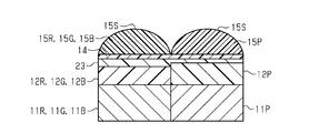
- the solid-state image sensor includes a solid-state image sensor filter 10 and a plurality of photoelectric conversion elements 11.
- the solid-state image sensor filter 10 includes filters 12R, 12G, and 12B for each color, an infrared cut filter 13 that is an example of an infrared filter, a barrier layer 14, and microlenses 15R, 15G, and 15B for each color.
- the filters 12R, 12G, 12B for each color are located between the photoelectric conversion element 11 for three colors and the infrared cut filter 13.
- the barrier layer 14 is located between the infrared cut filter 13 and the microlenses 15R, 15G, and 15B for each color.
- the infrared cut filter 13 is located on the light incident side with respect to each color filter 12R, 12G, 12B.
- the barrier layer 14 is located on the light incident side with respect to the infrared cut filter 13.
- the three-color photoelectric conversion element 11 includes a red photoelectric conversion element 11R, a green photoelectric conversion element 11G, and a blue photoelectric conversion element 11B.
- the solid-state imaging device includes a plurality of red photoelectric conversion elements 11R, a plurality of green photoelectric conversion elements 11G, and a plurality of blue photoelectric conversion elements 11B. In FIG. 1, one repeating unit of the photoelectric conversion element 11 in the solid-state imaging device is shown.
- the color filters for the three colors are composed of a red filter 12R, a green filter 12G, and a blue filter 12B.
- the red filter 12R is located on the light incident side with respect to the red photoelectric conversion element 11R.
- the green filter 12G is located on the light incident side with respect to the green photoelectric conversion element 11G.
- the blue filter 12B is located on the light incident side with respect to the blue photoelectric conversion element 11B.
- the thicknesses T12 of the filters 12R, 12G, 12B for the respective colors may be substantially equal to each other or may be different from each other. That is, the red filter 12R, the green filter 12G, and the blue filter 12B may not all have the same thickness.
- the thickness T12 of each color filter 12R, 12G, 12B is, for example, 0.5 ⁇ m or more and 5 ⁇ m or less.
- the infrared light cut function of the infrared cut filter 13 may change depending on the thickness T13 of the infrared cut filter 13.
- the thickness T13 of the infrared cut filter 13 may change depending on the level difference between the filters 12R, 12G, and 12B for each color. Therefore, from the viewpoint of improving the flatness of the infrared cut filter 13 on the base, it is preferable that the difference in the thickness T12 between the color filters 12R, 12G, and 12B is smaller than the thickness T13 of the infrared cut filter 13. ..
- the filters 12R, 12G, and 12B for each color are formed by forming a coating film containing a colored photosensitive resin and patterning the coating film using a photolithography method.
- a coating film containing a red photosensitive resin is formed by applying a coating liquid containing a red photosensitive resin and drying the coating film.
- the red filter 12R is formed by exposing and developing a coating film containing a red photosensitive resin.
- the red photosensitive resin is a negative photosensitive resin
- a portion of the coating film containing the red photosensitive resin corresponding to the area of the red filter 12R is exposed.
- the red photosensitive resin is a positive photosensitive resin
- a portion of the coating film containing the red photosensitive resin corresponding to a region other than the region of the red filter 12R is exposed. To be done.
- organic or inorganic pigments can be used alone or in combination of two or more.
- the pigment is preferably a pigment having high color development and high heat resistance, particularly a pigment having high thermal decomposition resistance.
- An organic pigment is usually used as the pigment.
- Pigments include, for example, phthalocyanine-based, azo-based, anthraquinone-based, quinacridone-based, dioxazine-based, ansanthuron-based, indanthrone-based, perylene-based, thioindigo-based, isoindoline-based, quinophthalone-based, and diketopyrrolopyrrole-based organics. It may be a pigment.
- the blue pigment used in the blue coloring composition of each color filter is, for example, CI Pigment Blue 15, 15:1, 15:2, 15:3, 15:4, 15:6, 16, 22, 60, 64, 81. May be a pigment such as. Of these, CI Pigment Blue 15:6 is preferable as the blue dye.
- the purple dye may be a pigment such as C.I. Pigment Violet 1, 19, 23, 27, 29, 30, 32, 37, 40, 42, 50. Among these, C.I. Pigment Violet 23 is preferable as the purple pigment.
- Yellow pigment is CI Pigment Yellow 1, 2, 3, 4, 5, 6, 10, 12, 13, 14, 15, 16, 17, 18, 24, 31, 32, 34, 35, 35:1, 36 , 36:1, 37, 37:1, 40, 42, 43, 53, 55, 60, 61, 62, 63, 65, 73, 74, 77, 81, 83, 93, 94, 95, 97, 98. , 100, 101, 104, 106, 108, 109, 110, 113, 114, 115, 116, 117, 118, 119, 120, 123, 126, 127, 128, 129, 138, 139, 147, 150, 151.
- C.I. Pigment Yellow 13, 150, 185 is preferable as the yellow dye.
- the red coloring composition is a composition obtained by using a red pigment and, if necessary, a pigment for toning, instead of the blue dye or the like.
- Red pigments include CI Pigment Red 7, 9, 14, 41, 48:1, 48:2, 48:3, 48:4, 81:1, 81:2, 81:3, 97, 122, 123, 146, 149, 168, 177, 178, 180, 184, 185, 187, 192, 200, 202, 208, 210, 215, 216, 217, 220, 223, 224, 226, 227, 228, 240, 246, 254, 255, 264, 272, CI Pigment Orange 36, 43, 51, 55, 59, 61, 71, 73 and the like.
- Pigments for toning are, for example, CI Pigment Yellow 1, 2, 3, 4, 5, 6, 10, 12, 13, 14, 15, 16, 17, 18, 24, 31, 32, 34, 35, 35:1, 36, 36:1, 37, 37:1, 40, 42, 43, 53, 55, 60, 61, 62, 63, 65, 73, 74, 77, 81, 83, 93, 94, 95, 97, 98, 100, 101, 104, 106, 108, 109, 110, 113, 114, 115, 116, 117, 118, 119, 120, 123, 126, 127, 128, 129, 138, 139, 147, 150, 151, 152, 153, 154, 155, 156, 161, 162, 164, 166, 167, 168, 169, 170, 171, 172, 173, 174, 175, 176, 177, 179, 180, 181, 182, 185, 187, 188, 193, 194, 198, 199
- the green coloring composition is a composition obtained by using a green pigment and a pigment for toning instead of the blue dye or the like.
- the green pigment may be, for example, C.I. Pigment Green 7, 10, 36, 37, 58, 59 or the like.
- the toning pigment may be a yellow pigment listed as a toning pigment in the red coloring composition.
- the infrared cut filter 13 cuts infrared light that can be detected by each photoelectric conversion element 11 with respect to the photoelectric conversion element 11, thereby increasing the detection accuracy of visible light by the photoelectric conversion element 11. That is, the infrared cut filter 13 suppresses the transmission of infrared light that can be detected by each photoelectric conversion element 11, with respect to the photoelectric conversion element 11.
- the infrared light that can be detected by each photoelectric conversion element 11 is, for example, near infrared light having a wavelength of 800 nm or more and 1000 nm or less.
- the infrared cut filter 13 is a layer common to the red filter 12R, the green filter 12G, and the blue filter 12B. That is, one infrared cut filter 13 covers the red filter 12R, the green filter 12G, and the blue filter 12B.
- the constituent material of the infrared cut filter 13 is a transparent resin containing an infrared absorbing dye.
- the infrared absorbing dye is, for example, an anthraquinone dye, a cyanine dye, a phthalocyanine dye, a dithiol dye, a diimonium dye, a squarylium dye, or a croconium dye.
- the transparent resin is, for example, an acrylic resin, a polyamide resin, a polyimide resin, a polyurethane resin, a polyester resin, a polyether resin, a polyolefin resin, a polycarbonate resin, a polystyrene resin, or a norbornene resin.
- the infrared cut filter 13 is formed by film formation using a coating method or the like.
- the transmission spectrum of the infrared cut filter 13 preferably satisfies the following conditions [A1] to [A3].
- the average transmittance is 80% or more in the wavelength band of 450 nm or more and 650 nm or less.
- [A2] Has maximum absorption in the wavelength band of 800 nm or more and 1000 nm or less.
- the cutoff wavelength width which is the difference between the cutoff wavelength on the short wavelength side having a transmittance of 50% and the cutoff wavelength on the long wavelength side having a transmittance of 50%, is 100 nm or more.
- the structure satisfies [A1] If the structure satisfies [A1], absorption of visible light by the infrared cut filter 13 is sufficiently suppressed. With the configuration that satisfies [A2] and [A3], the near-infrared light that can be detected by the photoelectric conversion element 11 for each color is sufficiently cut by the infrared cut filter 13.
- the barrier function of the oxidation source by the barrier layer 14 may change depending on the thickness of the barrier layer 14.
- the thickness of the barrier layer 14 on the infrared cut filter 13 may change depending on the step on the upper surface of the infrared cut filter 13. Therefore, from the viewpoint of improving the flatness of the barrier layer 14 in the base, the thickness T13 of the infrared cut filter 13 is preferably a size that provides suitable flatness to the upper surface of the infrared cut filter 13. .. Suitable flatness is, for example, that the step on the upper surface of the infrared cut filter 13 is smaller than three times the thickness of the barrier layer 14.
- the infrared absorption dyes mentioned above come into contact with oxygen and water in the atmosphere under the environment where sunlight is irradiated, which changes the transmission spectrum in the near infrared band. That is, the infrared cut filter 13 comes into contact with the oxidation source under the environment where sunlight is irradiated, and reduces the near infrared light cut performance.
- the barrier layer 14 suppresses the permeation of oxygen and water, which are the oxidation sources of the infrared cut filter 13, thereby suppressing the deterioration of the near infrared light cut performance due to the infrared absorbing dye, and the visible light Suppresses deterioration of transmission performance.
- the barrier layer 14 is a layer common to the red filter 12R, the green filter 12G, and the blue filter 12B. That is, one barrier layer 14 covers the red filter 12R, the green filter 12G, and the blue filter 12B.
- the constituent material of the barrier layer 14 may be an inorganic compound.
- the constituent material of the barrier layer 14 is preferably a silicon compound.
- the constituent material of the barrier layer 14 is, for example, at least one selected from the group consisting of silicon nitride, silicon oxide, and silicon oxynitride.
- the barrier layer 14 is formed by a vapor deposition method such as a sputtering method, a CVD method or an ion plating method, or a liquid phase deposition method such as a coating method.
- the barrier layer 14 made of silicon oxide is formed on the substrate on which the infrared cut filter 13 is formed by film formation by sputtering using a target made of silicon oxide.
- the barrier layer 14 made of silicon oxide is formed on the substrate on which the infrared cut filter 13 is formed by the film formation by the CVD using silane and oxygen.
- the barrier layer 14 made of silicon oxide is formed by applying a coating liquid containing polysilazane, modifying the coating liquid, and drying the coating film.
- the oxygen transmittance, the thickness, and the visible light region transmittance of the barrier layer 14 satisfy the following conditions [B1] or [B3].
- the oxygen permeability according to JIS K 7126-2:2006 is 5.0 cc/m 2 /day/atm or less. In other words, the oxygen permeability is 5.0 cm 3 /m 2 /day/atm or less.
- the oxygen permeability is based on JIS K 7126-2:2006, Annex A, and is the oxygen permeability at 23° C. and 50% relative humidity.
- the thickness of the barrier layer 14 is 10 nm or more and 500 nm or less.
- the visible light region transmittance (average) of the barrier layer 14 is 90% or more.
- the oxygen permeability is preferably not more than 3.0cc / m 2 / day / atm , 1.0cc / m 2 / day / atm or less Is more preferable and 0.7 cc/m 2 /day/atm or less is further preferable.
- the oxygen permeability is preferably 3.0 cm 3 /m 2 /day/atm or less, more preferably 1.0 cm 3 /m 2 /day/atm or less, 0.7 cm 3 / It is more preferably m 2 /day/atm or less.
- composition satisfies [B2]
- the barrier layer 14 may have a single-layer structure composed of a single compound, may have a laminated structure composed of layers composed of a single compound, or may have a laminated structure composed of layers composed of mutually different compounds. May have.
- the barrier layer 14 may have a structure satisfying [B1] by providing a laminated structure of layers that do not satisfy [B1] in a single layer.
- each color microlens includes a red microlens 15R, a green microlens 15G, and a blue microlens 15B.
- the red microlens 15R is located on the light incident side with respect to the red filter 12R.
- the green microlens 15G is located on the light incident side with respect to the green filter 12G.
- the blue microlens 15B is located on the light incident side with respect to the blue filter 12B.
- the microlenses 15R, 15G, and 15B for each color have an incident surface 15S that is an outer surface.
- the microlenses 15R, 15G, 15B for the respective colors have a predetermined refractive index difference with respect to the refractive index of the outside air in order to collect the light entering the incident surface 15S toward the photoelectric conversion elements 11R, 11G, 11B for the respective colors.
- the microlenses 15R, 15G, 15B for each color are formed by forming a coating film containing a transparent resin, patterning the coating film using a photolithography method, and reflowing by heat treatment.
- the transparent resin is, for example, an acrylic resin, a polyamide resin, a polyimide resin, a polyurethane resin, a polyester resin, a polyether resin, a polyolefin resin, a polycarbonate resin, a polystyrene resin, or a norbornene resin.
- the following effects can be obtained. (1-1) Since the barrier layer 14 prevents the oxidation source from reaching the infrared cut filter 13, the infrared cut filter 13 is less likely to be oxidized by the oxidation source. As a result, the light resistance of the infrared cut filter 13 and thus the light resistance of the solid-state imaging device can be improved.
- the thickness T13 of the infrared cut filter 13 is of a size that gives suitable flatness to the upper surface of the infrared cut filter 13, it conforms to (1-1) and (1-2) above. It is also possible to suppress the variation in the effect.
- the first embodiment can be modified and implemented as follows. [First modification] As shown in FIG. 3, the barrier layer 14 is located not only between the infrared cut filter 13 and the microlenses 15R, 15G, 15B for each color but also on the outer surface of the microlenses 15R, 15G, 15B for each color. You may. At this time, the outer surface of the barrier layer 14 functions as an incident surface on which light is incident on the solid-state image sensor. The point is that the position of the barrier layer 14 may be on the light incident side with respect to the infrared cut filter 13.
- the barrier layer 14 is located on the optical surface (flat surface) of the microlenses 15R, 15G, 15B for each color. As a result, it is easy to make the thickness of the barrier layer 14 uniform, and it is also easy to make the barrier function of the oxidation source by the barrier layer 14 uniform.
- the refractive index of the barrier layer 14 be lower than the refractive index of the microlenses 15R, 15G, 15B for each color. Further, the difference between the refractive index of the microlenses 15R, 15G, 15B for each color and the refractive index of the barrier layer 14 is more preferably 0.1 or more. According to this configuration, the difference in refractive index between air and the microlenses for each color can be reduced, so that it is possible to suppress the reflected light generated on the incident surface side.
- the barrier layer 14 preferably also has a function of preventing reflection of visible light. If the barrier layer 14 also has the antireflection function, it is possible to suppress a decrease in detection sensitivity due to reflection on the incident surface. In addition, since the barrier layer 14 that suppresses the transmission of the oxidation source also has an antireflection function, it is possible to simplify the layer structure of the solid-state image sensor filter 10 as compared with a configuration in which an antireflection layer is separately provided. ..
- the antireflection function may be realized by a difference in refractive index between the barrier layer 14 and another layer, or the barrier layer 14 includes a filler and imparts an embossed shape to the barrier layer 14. Accordingly, the barrier layer 14 may be realized by having an uneven shape.
- the layers other than the infrared cut filter 13 can also have the cut function of the infrared cut filter 13.
- the microlenses 15R, 15G, and 15B for each color can also have the cut function of the infrared cut filter. That is, in the solid-state image sensor filter 10, the constituent materials of the microlenses 15R, 15G, and 15B for each color can include an infrared absorbing dye. As a result, the solid-state image sensor filter 10 can be changed to a configuration in which the infrared cut filter 13 is omitted.
- microlenses 15R, 15G, and 15B for each color also have an infrared cut function, the layered structure of the solid-state image sensor filter 10 can be simplified.
- the filters 12R, 12G, and 12B for the respective colors tend to have mutually different thicknesses in order to convert lights of mutually different colors into the same intensity.
- the filter for one color tends to form a step with the filter for another color.
- the infrared cut filter 13 is likely to have a shape that follows the step formed between the different color filters.
- the shape of the infrared cut filter 13 that follows the step causes the thickness of the barrier layer 14 to vary, which in turn causes the barrier function of the oxidation source to vary.
- the solid-state image sensor filter 10 may include a flattening layer 21 separately between the infrared cut filter 13 and the barrier layer 14.
- the flattening layer 21 has a light-transmitting property of transmitting visible light, and the surface of the flattening layer 21 has a flat surface that fills the step formed by the infrared cut filter 13. That is, the flattening layer 21 has a shape capable of relaxing the height difference of the surface of the infrared cut filter 13.
- the constituent material of the flattening layer 21 is a transparent resin.
- the transparent resin is, for example, an acrylic resin, a polyamide resin, a polyimide resin, a polyurethane resin, a polyester resin, a polyether resin, a polyolefin resin, a polycarbonate resin, a polystyrene resin, or a norbornene resin.
- the flattening layer 21 is formed by film formation using a liquid phase film formation method such as a coating method.
- the solid-state image sensor filter 10 is configured to additionally include the flattening layer 21, the effect according to (1-3) above can be obtained, and the thickness T13 of the infrared cut filter 13 and It is also possible to remove the constraint of flattening due to these from the thickness T12 of each color filter 12R, 12G, 12B.
- the solid-state image sensor filter 10 may include a flattening layer 22 between the color filters 12R, 12G, and 12B and the infrared cut filter 13.
- the constituent material and the forming method of the flattening layer 22 may be the same as the constituent material and the forming method described in the third modification.
- the position of the infrared cut filter 13 is not limited to the position between the filters 12R, 12G, 12B for each color and the barrier layer 14.
- the position of the infrared cut filter 13 may be changed, for example, between each photoelectric conversion element 11 and each color filter 12R, 12G, 12B.
- the position of the infrared cut filter 13 may be between the barrier layer 14 and each photoelectric conversion element 11.
- the position of the infrared cut filter 13 and the position of the barrier layer 14 are not limited to between the microlenses 15R, 15G, 15B for each color and the filters 12R, 12G, 12B for each color. ..
- the position of the infrared cut filter 13 and the position of the barrier layer 14 may be changed between each color filter 12R, 12G, 12B and each photoelectric conversion element 11. In short, the position of the infrared cut filter 13 and the position of the barrier layer 14 may be on the light incident side with respect to each photoelectric conversion element 11.
- the plurality of photoelectric conversion elements 11 can include an infrared photoelectric conversion element 11P for measuring the intensity of infrared light.
- the solid-state image sensor filter 10 includes an infrared pass filter 12P on the light incident side with respect to the infrared photoelectric conversion element 11P.
- the infrared pass filter 12P cuts visible light that can be detected by the infrared photoelectric conversion element 11P with respect to the infrared photoelectric conversion element 11P, thereby increasing the accuracy of infrared light detection by the infrared photoelectric conversion element 11P. ..
- the infrared light that can be detected by the infrared photoelectric conversion element 11P is, for example, near infrared light having a wavelength of 800 nm or more and 1200 nm or less.
- the infrared pass filter 12P is formed by forming a coating film containing a black photosensitive resin and patterning the coating film using a photolithography method.
- the infrared cut filter 13 is provided with a through hole 13H on the light incident side of the infrared pass filter 12P, so that the infrared cut filter 13 is not located on the light incident side of the infrared pass filter 12P.
- the infrared cut filter 13 is common to the red filter 12R, the green filter 12G, and the blue filter 12B. That is, one infrared cut filter 13 covers the red filter 12R, the green filter 12G, and the blue filter 12B.
- the through hole 13H included in the infrared cut filter 13 is formed by a processing method such as patterning using a photolithography method or a dry etching method.
- a photosensitive composition containing an infrared absorbing dye is used as a constituent material of the infrared cut filter 13.
- the photosensitive composition may include a binder resin, a photopolymerization initiator, a polymerizable monomer, an organic solvent, a leveling agent and the like.
- the binder resin may be, for example, acrylic resin, polyamide resin, polyimide resin, polyurethane resin, polyester resin, polyether resin, polyolefin resin, polycarbonate resin, polystyrene resin, norbornene resin. ..
- the photopolymerization initiator is an acetophenone photopolymerization initiator, a benzoin photopolymerization initiator, a benzophenone photopolymerization initiator, a thioxanthone photopolymerization initiator, a triazine photopolymerization initiator, an oxime ester photopolymerization initiator, or the like. You can As the photopolymerization initiator, one of these photopolymerization initiators may be used alone, or two or more thereof may be mixed and used.
- the polymerizable monomer is (meth)acrylic acid, methyl (meth)acrylate, ethyl (meth)acrylate, propyl (meth)acrylate, isopropyl (meth)acrylate, butyl (meth)acrylate, isobutyl (meth)acrylate, tert-butyl.
- organic solvent examples include ethyl lactate, benzyl alcohol, 1,2,3-trichloropropane, 1,3-butanediol, 1,3-butylene glycol, 1,3-butylene glycol diacetate, 1,4-dioxane, 2-heptanone, 2-methyl-1,3-propanediol, 3,5,5-trimethyl-2-cyclohexen-1-one, 3,3,5-trimethylcyclohexanone, ethyl 3-ethoxypropionate, 3-methyl -1,3-butanediol, 3-methoxy-3-methyl-1-butanol, 3-methoxy-3-methylbutyl acetate, 3-methoxybutanol, 3-methoxybutyl acetate, 4-heptanone, m-xylene, m -Diethylbenzene, m-dichlorobenzene, N,N-dimethylacetamide, N,N-dimethylform
- the leveling agent is preferably dimethylsiloxane having a polyether structure or a polyester structure in the main chain.
- the dimethyl siloxane having a polyether structure in the main chain may be, for example, FZ-2122 manufactured by Toray Dow Corning, BYK-333 manufactured by BYK Chemie.
- the dimethyl siloxane having a polyester structure may be, for example, BYK-310 and BYK-370 manufactured by BYK Chemie. Both dimethylsiloxane having a polyether structure and dimethylsiloxane having a polyester structure may be used as the leveling agent.
- the leveling agent one of these may be used alone, or two or more of them may be mixed and used.
- the constituent material of the infrared cut filter 13 is a curable composition containing an infrared absorbing dye.
- the curable composition includes a transparent resin.
- the transparent resin may be, for example, acrylic resin, polyamide resin, polyimide resin, polyurethane resin, polyester resin, polyether resin, polyolefin resin, polycarbonate resin, polystyrene resin, norbornene resin. ..
- the barrier layer 14 includes a through hole 14H on the light incident side of the infrared pass filter 12P. As a result, the barrier layer 14 is not located on the light incident side of the infrared pass filter 12P.
- the barrier layer 14 is common to the red filter 12R, the green filter 12G, and the blue filter 12B. That is, one barrier layer 14 covers the red filter 12R, the green filter 12G, and the blue filter 12B.
- any processing method may be used as long as it is a method capable of penetrating the barrier layer 14 to form a hole.
- a dry etching method or the like is used to form the through holes 14H.
- the filters 12R, 12G, 12B for each color are thinner than the infrared pass filter 12P.
- the sum of the thickness of the infrared cut filter 13 and the thickness of the barrier layer 14 corresponds to the difference between the thickness of each color filter 12R, 12G, 12B and the thickness of the infrared pass filter 12P.
- the light resistance of the infrared cut filter 13 can be improved, and the visible light is measured by the photoelectric conversion elements 11R, 11G, and 11B for each color, and the infrared photoelectric conversion is performed. Infrared light can be measured by the element 11P.
- the thickness of the infrared pass filter 12P that cuts visible light is likely to be larger than the thickness of each color filter 12R, 12G, 12B.
- the step TP between the infrared pass filter 12P and each color filter 12R, 12G, 12B is filled with the infrared cut filter 13 and the barrier layer 14. Therefore, even if the step TP is generated between the filters 12R, 12G, 12B for each color and the infrared pass filter 12P, the microlenses 15R, 15G, 15B for each color and the lower layer of the microlens 15P for infrared are provided. It is easy to obtain flatness.
- the solid-state image sensor may include an anchor layer between the barrier layer 14 and the lower layer of the barrier layer 14. Thereby, the adhesion between the barrier layer 14 and the lower layer of the barrier layer 14 can be enhanced by the anchor layer.
- the solid-state imaging device may include an anchor layer between the barrier layer 14 and the upper layer of the barrier layer 14. Thereby, the adhesion between the barrier layer 14 and the upper layer of the barrier layer 14 can be enhanced by the anchor layer.
- the constituent material of the anchor layer is, for example, a polyfunctional acrylic resin or a silane coupling agent.
- the thickness of the anchor layer is, for example, 50 nm or more and 1 ⁇ m or less. When the thickness of the anchor layer is 50 nm or more, it is easy to obtain adhesion between the layers. When the thickness of the anchor layer is 1 ⁇ m or less, it is easy to suppress light absorption in the anchor layer.
- the plurality of photoelectric conversion elements 11 may be composed of an organic photoelectric conversion element and an inorganic photoelectric conversion element. This makes it possible to omit the filters 12R, 12G, 12B for the respective colors. Even if the filters 12R, 12G, and 12B for each color are omitted, the solid-state image sensor filter 10 includes the infrared cut filter 13 and the above-described barrier function, so that the infrared cut filter 13 is provided. It is possible to protect the cut function of.
- the solid-state image sensor filter 10 may include a black matrix and a flattening layer between the plurality of photoelectric conversion elements 11 and the color filters 12R, 12G, and 12B.
- the black matrix suppresses the light of each color selected by the filters 12R, 12G, and 12B for each color from entering the photoelectric conversion elements 11 for other colors.
- the flattening layer fills the step difference of the black matrix, thereby flattening the base of each of the color filters 12R, 12G, and 12B and the base of the infrared cut filter 13. As a result, the planarization layer planarizes the base of the barrier layer 14.
- the color filter may be changed to a three-color filter composed of a cyan filter, a yellow filter, and a magenta filter.
- the color filter may be changed to a four-color filter including a cyan filter, a yellow filter, a magenta filter, and a black filter.
- the color filter may be changed to a four-color filter including a transparent filter, a yellow filter, a red filter, and a black filter.
- the refractive index of each color filter 12R, 12G, 12B is, for example, 1.6 or more and 1.9 or less.
- the refractive index of each microlens 15R, 15G, 15B is, for example, 1.4 or more and 2.0 or less. More preferably, the refractive index of each microlens 15R, 15G, 15B is 1.5 or more and 1.7 or less.
- the constituent materials of the infrared cut filter 13 and the infrared pass filter 12P are made of an inorganic material in order to suppress the difference from the refractive index of each color filter 12R, 12G, 12B and each microlens 15R, 15G, 15B. It may contain oxide particles.
- the inorganic oxide is, for example, aluminum oxide, silicon oxide, zirconium oxide, or titanium oxide.
- the constituent materials of the infrared cut filter 13 and the infrared pass filter 12P may contain additives for having other functions such as a light stabilizer, an antioxidant, a heat stabilizer, and an antistatic agent. ..
- the solid-state imaging device has a structure in which the barrier layer 14 is omitted, and the oxygen transmittance of the laminated structure located on the incident surface 15S side with respect to the infrared cut filter 13 is 5.0 cc/m 2 / It is possible to change the configuration to be less than day/atm.
- the laminated structure includes filters 12R, 12G, 12B for each color, a flattening layer, and microlenses 15R, 15G, 15B for each color, and the oxygen transmission rate of the laminated structure is 5.0 cc/m 2 /day/ It may be less than or equal to atm.
- FIG. 10 is a schematic configuration diagram in which each layer in a part of the solid-state imaging device is shown separately.
- the solid-state image sensor includes a solid-state image sensor filter 10 and a plurality of photoelectric conversion elements 11.
- the solid-state image sensor filter 10 includes filters 12R, 12G, 12B for respective colors, an infrared pass filter 12P, a barrier layer 14, and microlenses 15R, 15G, 15B, 15P.
- the infrared pass filter 12P is an example of an infrared filter.
- the filters 12R, 12G, 12B for each color are located between the photoelectric conversion elements 11R, 11G, 11B for three colors and the microlenses 15R, 15G, 15B.
- the infrared pass filter 12P is located between the infrared photoelectric conversion element 11P and the microlens 15P.
- the barrier layer 14 is located between the infrared pass filter 12P and the infrared microlens 15P. The barrier layer 14 is located on the light incident side with respect to the infrared pass filter 12P.
- the three-color photoelectric conversion element 11 is an example of a first photoelectric conversion element, and includes a red photoelectric conversion element 11R, a green photoelectric conversion element 11G, and a blue photoelectric conversion element 11B.
- the infrared photoelectric conversion element 11P is an example of a second photoelectric conversion element.
- the solid-state imaging device includes a plurality of red photoelectric conversion elements 11R, a plurality of green photoelectric conversion elements 11G, a plurality of blue photoelectric conversion elements 11B, and a plurality of infrared photoelectric conversion elements 11P.
- FIG. 10 shows one repeating unit of the photoelectric conversion element 11 in the solid-state image sensor.
- the thickness T12 of each color filter 12R, 12G, 12B may be different from that of the infrared pass filter 12P, or may be equal to each other.
- the thickness T12 of each color filter 12R, 12G, 12B is, for example, 0.5 ⁇ m or more and 5 ⁇ m or less.
- the infrared light transmitting function of the infrared pass filter 12P may change depending on the thickness T12 of the infrared pass filter 12P.
- the microlenses 15R, 15G, 15B on the filters 12R, 12G, 12B for the respective colors and the microlens 15P on the barrier layer 14 are formed by the steps between the filters 12R, 12G, 12B for the respective colors and the barrier layer 14. Can reduce the accuracy of the processing.
- the total of the thickness T12 of the infrared pass filter 12P and the thickness T14 of the barrier layer 14 is the filter 12R for each color, It is preferable that the thickness is substantially equal to that of 12G and 12B.
- the infrared pass filter 12P cuts visible light that the infrared photoelectric conversion element 11P can detect with respect to the infrared photoelectric conversion element 11P, thereby detecting the near infrared light with the infrared photoelectric conversion element 11P. Increase. That is, the infrared pass filter 12P suppresses transmission of visible light that the infrared photoelectric conversion element 11P can detect with respect to the infrared photoelectric conversion element 11P.
- the infrared pass filter 12P is a layer located only on the infrared photoelectric conversion element 11P.
- the constituent material of the infrared pass filter 12P includes a black pigment or a black dye and a transparent resin.
- the black pigment is a single pigment having a black color or a mixture having two or more pigments having a black color.
- the black dye is, for example, an azo dye, anthraquinone dye, azine dye, quinoline dye, perinone dye, perylene dye, or methine dye.
- the transparent resin is, for example, an acrylic resin, a polyamide resin, a polyimide resin, a polyurethane resin, a polyester resin, a polyether resin, a polyolefin resin, a polycarbonate resin, a polystyrene resin, or a norbornene resin.
- the infrared pass filter 12P is formed by film formation using a liquid phase film formation method such as a coating method.
- the constituent material of the infrared pass filter 12P may contain particles of an inorganic oxide for adjusting the refractive index of the infrared pass filter 12P.
- the inorganic oxide is, for example, aluminum oxide, silicon oxide, zirconium oxide, or titanium oxide.
- the infrared pass filter 12P may contain an additive such as a light stabilizer, an antioxidant, a heat stabilizer, and an antistatic agent, which has other functions.
- the transmission spectrum of the infrared pass filter 12P shows a transmittance of 3% or less in the wavelength range of 400 nm to 700 nm, for example.
- the infrared pass filter 12P has a transmittance of 10% or more with a wavelength of 850 nm as a peak, and a transmittance of 90% or more at a wavelength of 900 nm or more.
- the solar spectrum has an absorption band near the wavelength of 940 nm due to the absorption of water vapor. Therefore, the spectrum intensity in the sunlight spectrum decreases near the wavelength of 940 nm. Therefore, near-infrared light having a wavelength of 940 nm is less likely to be affected by sunlight as ambient light when the solid-state image sensor is used outdoors and in the daytime. In other words, if the center wavelength of the light source used is 940 nm, it is possible to provide a solid-state image sensor with less noise.
- the infrared photoelectric conversion element 11P detects near-infrared light having a wavelength of 940 nm.
- the barrier layer 14 suppresses the permeation of oxygen and water, which are oxidation sources of the infrared pass filter 12P, thereby suppressing the deterioration of the visible light cut performance due to the black pigment and the black dye, and the near infrared light. Suppresses the deterioration of the permeation performance.
- the barrier layer 14 is located on the incident surface 15S side with respect to the infrared pass filter 12P, and is not located on the incident surface 15S side with respect to each color filter 12R, 12G, 12B. That is, the barrier layer 14 covers the infrared pass filter 12P, but does not cover the filters 12R, 12G, and 12B for the respective colors.
- the oxygen permeability, the thickness, and the visible light region transmittance of the barrier layer 14 satisfy the above condition [B1] or [B3].
- the oxygen permeability is preferably not more than 3.0cc / m 2 / day / atm , 1.0cc / m 2 / day / atm or less Is more preferable and 0.7 cc/m 2 /day/atm or less is further preferable.
- composition satisfies [B2]
- the constituent materials that satisfy [B1] and [B3]. Further, it is possible to suppress the occurrence of cracks in the barrier layer 14. If the structure satisfies [B3], absorption of visible light by the barrier layer 14 is sufficiently suppressed.
- the barrier layer 14 prevents the oxidation source from reaching the infrared pass filter 12P, the infrared pass filter 12P is less likely to be oxidized by the oxidation source. As a result, the light resistance of the infrared pass filter 12P and thus the light resistance of the solid-state image sensor can be improved.
- the microlenses 15R, 15G, 15B. , 15P high flatness can be obtained. As a result, it is possible to suppress variations in processing and shapes of the microlenses 15R, 15G, 15B, 15P.
- the barrier layer 14 may be arranged on the light incident side with respect to the infrared pass filter 12P and the filters 12R, 12G, and 12B for each color. That is, the barrier layer 14 may be arranged on the entire incident surface 15S side with respect to each photoelectric conversion element 11.
- the barrier layer 14 is located on the entire incident surface 15S side with respect to each photoelectric conversion element 11, the barrier layer 14 is formed over the entire film formation target by using the method. It is possible to form 14. Further, since it is not necessary to separately remove the barrier layer 14 from the filters 12R, 12G, and 12B for the respective colors, it is possible to simplify the method for forming the solid-state imaging device.
- the infrared pass filter 12P that cuts all wavelength regions of visible light tends to have a different thickness from the filters 12R, 12G, and 12B for each color.
- the infrared pass filter 12P is likely to form a step between each color filter 12R, 12G, 12B.
- the upper surface of the infrared pass filter 12P and a part of the peripheral surface are exposed from the filters 12R, 12G, and 12B for each color.
- the barrier layer 14 When the barrier layer 14 is located on the entire incident surface 15S side of each photoelectric conversion element 11 as in the first modification, the barrier layer 14 includes the infrared pass filter 12P and the filters 12R, 12G for the respective colors. Between 12B and 12B, it is easy to have a shape that follows the step. The shape of the barrier layer 14 that follows the step causes variations in the thickness of the barrier layer 14, which in turn causes variations in the barrier function of the oxidation source. In particular, there is a possibility that the barrier function of the oxidation source may be deteriorated at a part of the peripheral surface of the infrared pass filter 12P.
- the flattening layer 23 has a light-transmitting property of transmitting visible light, and the surface of the flattening layer 23 has a flat surface that fills the step formed by the infrared pass filter 12P. That is, the flattening layer 23 has a shape capable of relaxing the height difference formed by the infrared pass filter 12P and the filters 12R, 12G, 12B for the respective colors.
- the constituent material of the flattening layer 23 may be a material that can be used for the flattening layer 21 of the first embodiment. (2-6) If the flattening layer 23 is separately provided, even if a part of the peripheral surface of the infrared pass filter 12P is exposed from each color filter 12R, 12G, 12B, the above (2) It is also possible to obtain the effects according to -1) and (2-5).
- the solid-state image sensor includes an infrared cut filter 13 separately.
- the infrared cut filter 13 cuts infrared light that can be detected by the photoelectric conversion elements 11R, 11G, and 11B for each color, thereby increasing the detection accuracy of visible light by the photoelectric conversion element 11.
- the infrared light that can be detected by each photoelectric conversion element 11 is, for example, near infrared light having a wavelength of 800 nm or more and 1000 nm or less.
- the infrared cut filter 13 is a layer common to the red filter 12R, the green filter 12G, and the blue filter 12B. That is, one infrared cut filter 13 covers the red filter 12R, the green filter 12G, and the blue filter 12B.
- the infrared cut filter 13 is located on the light incident side with respect to each color filter 12R, 12G, 12B.
- the infrared cut filter 13 includes a through hole 13H on the light incident side of the infrared pass filter 12P and is not located on the light incident side of the infrared pass filter 12P.
- the infrared cut function of the infrared cut filter 13 may vary depending on the thickness of the infrared cut filter 13.
- the thickness of the infrared cut filter 13 may vary depending on the level difference between the filters 12R, 12G, 12B for each color and between the filters 12R, 12G, 12B for each color. Therefore, from the viewpoint that the flatness of the base of the infrared cut filter 13 is enhanced, it is preferable that the difference in thickness between the filters 12R, 12G, and 12B for each color is smaller than the thickness of the infrared cut filter 13.
- each color filter 12R, 12G, 12B is thinner than the infrared pass filter 12P.
- the infrared cut filter 13 preferably has a thickness corresponding to the film thickness difference between the filters 12R, 12G, 12B for the respective colors and the infrared pass filter 12P.
- the surface of the infrared pass filter 12P on the incident surface side and the surface of the infrared cut filter 13 on the incident surface side are located at the same height. That is, the surface of the infrared pass filter 12P in contact with the barrier layer 14 and the surface of the infrared cut filter 13 in contact with the barrier layer 14 are located at the same height. In other words, the incident surface side surface of the infrared pass filter 12P and the incident surface side surface of the infrared cut filter 13 are flush with each other.
- the transmission spectrum of the infrared cut filter 13 preferably satisfies the above conditions [A1] to [A3].
- [A1] absorption of visible light by the infrared cut filter 13 is sufficiently suppressed.
- [A2] and [A3] near-infrared light that can be detected by the photoelectric conversion element 11 for each color is sufficiently cut by the infrared cut filter 13, and visible light is cut. Suffering is sufficiently suppressed.
- Infrared absorbing dye comes into contact with oxygen and water in the atmosphere under the environment where sunlight is irradiated, which changes the transmission spectrum in the near infrared band. That is, the infrared cut filter 13 comes into contact with the oxidation source under the environment where sunlight is irradiated, and reduces the near infrared light cut performance. In this respect, since the barrier layer 14 is also located on the incident surface 15S side of the infrared cut filter 13, it is possible to improve the light resistance of the infrared cut filter 13.
- the barrier layer 14 can be located not only between the infrared pass filter 12P and the infrared microlens 15P but also on the outer surface of the infrared microlens 15P. At this time, the outer surface of the barrier layer 14 functions as an incident surface on which light is incident on the solid-state image sensor. In short, the position of the barrier layer 14 may be on the light incident side with respect to the infrared pass filter 12P. According to this configuration, the barrier layer 14 is located on the optical surface (flat surface) of the infrared microlens 15P. As a result, it is easy to make the thickness of the barrier layer 14 uniform, and it is easy to make the barrier function of the oxidation source by the barrier layer 14 uniform.
- the solid-state image sensor may include an anchor layer between the barrier layer 14 and the layer below the barrier layer 14. Thereby, the adhesion between the barrier layer 14 and the lower layer of the barrier layer 14 can be enhanced by the anchor layer.
- the solid-state imaging device may include an anchor layer between the barrier layer 14 and the upper layer of the barrier layer 14. Thereby, the adhesion between the barrier layer 14 and the upper layer of the barrier layer 14 can be enhanced by the anchor layer.
- the constituent material and thickness of the anchor layer may be the same as the constituent material and thickness of the anchor layer in the modification of the first embodiment.
- the plurality of photoelectric conversion elements 11 are composed of an organic photoelectric conversion element and an inorganic photoelectric conversion element, so that the filters 12R, 12G, 12B for each color may be omitted in the solid-state image sensor filter 10. Even if the filters 12R, 12G, and 12B for each color are omitted, if the configuration includes the infrared pass filter 12P, the transmission function of the infrared pass filter 12P is protected by providing the above-described barrier function. It is possible.
- the solid-state image sensor filter 10 may include a black matrix and a flattening layer between the photoelectric conversion elements 11 and the color filters 12R, 12G, 12B, and the infrared pass filter 12P. Good.
- the black matrix suppresses the light of each color selected by the filters 12R, 12G, and 12B for each color from entering the photoelectric conversion elements 11 for other colors.
- the flattening layer fills the step difference of the black matrix, and thereby flattens the base of each color filter 12R, 12G, 12B, the base of the infrared pass filter 12P, and the base of the infrared cut filter 13.
- the planarization layer planarizes the base of the barrier layer 14.
- the color filter may be changed to a three-color filter composed of a cyan filter, a yellow filter, and a magenta filter.
- the color filter may be changed to a four-color filter including a cyan filter, a yellow filter, a magenta filter, and a black filter.
- the color filter may be changed to a four-color filter including a transparent filter, a yellow filter, a red filter, and a black filter.
- the refractive index of each color filter 12R, 12G, 12B is, for example, 1.7 or more and 1.9 or less.
- the refractive index of each microlens 15R, 15G, and 15B is, for example, 1.5 or more and 1.6 or less.
- the constituent materials of the infrared pass filter 12P and the infrared cut filter 13 are particles of an inorganic oxide in order to suppress a difference from the refractive index of each color filter 12R, 12G, 12B and each microlens 15R, 15G, 15B. Can be included.
- the inorganic oxide is, for example, aluminum oxide, silicon oxide, zirconium oxide, or titanium oxide.
- the constituent materials of the infrared pass filter 12P and the infrared cut filter 13 may contain additives for having other functions such as a light stabilizer, an antioxidant, a heat stabilizer, and an antistatic agent. ..
- the solid-state image sensor has a structure in which the barrier layer 14 is omitted, and has an oxygen transmission rate of 5.0 cc/m 2 /in a laminated structure located on the incident surface 15S side with respect to the infrared pass filter 12P. It is possible to change the configuration to be less than day/atm.
- the laminated structure is formed by other functional layers such as a flattening layer and an adhesion layer.
- the laminated structure may form a structure having an oxygen transmittance of 5.0 cc/m 2 /day/atm or less together with the infrared microlens 15P.
- the solid-state image sensor may have a bandpass filter separately on the light incident surface side with respect to the plurality of microlenses.
- the bandpass filter is a filter that transmits a specific wavelength in visible light and near infrared light, and has the same function as the infrared cut filter 13. That is, the bandpass filter can cut off unnecessary infrared light that can be detected by the photoelectric conversion elements 11R, 11G, 11B for each color and the infrared photoelectric conversion element 11P.
Landscapes
- Physics & Mathematics (AREA)
- General Physics & Mathematics (AREA)
- Optics & Photonics (AREA)
- Health & Medical Sciences (AREA)
- Toxicology (AREA)
- Solid State Image Pick-Up Elements (AREA)
- Optical Filters (AREA)
- Developing Agents For Electrophotography (AREA)
- Color Television Image Signal Generators (AREA)
Abstract
Description
以下、固体撮像素子用フィルター、および、固体撮像素子の第1実施形態を、図1および図2を参照して説明する。図1は、固体撮像素子の一部における各層を分離して示す概略構成図である。なお、図1および図2が示す構造はいずれも、固体撮像素子の構造における一例である。図1が示すように、固体撮像素子が備える各色用フィルター間には隙間が位置してもよいし、図2が示すように、各色用フィルター間には隙間が位置しなくてもよい。
各色用フィルターの青色着色組成物に用いられる青色色素は、例えばC.I. Pigment Blue 15、15:1、15:2、15:3、15:4、15:6、16、22、60、64、81などの顔料であってよい。これらのなかでもC.I. Pigment Blue 15:6が青色色素として好ましい。
[A2]800nm以上1000nm以下の波長帯において最大吸収を有する。
[A3]50%の透過率を有する短波長側のカットオフ波長と、50%の透過率を有する長波長側のカットオフ波長との差であるカットオフ波長幅が100nm以上である。
[B1]JIS K 7126-2:2006に準拠した酸素透過率が5.0cc/m2/day/atm以下である。言い換えれば、当該酸素透過率が、5.0cm3/m2/day/atm以下である。なお、酸素透過率は、JIS K 7126-2:2006の付属書Aに準拠し、かつ、23℃かつ相対湿度50%における酸素透過率である。
[B2]バリア層14の厚みが10nm以上500nm以下である。
[B3]バリア層14の可視光領域透過率(平均)が90%以上である。
(1‐1)赤外カットフィルター13に酸化源が到達することをバリア層14が抑制するため、赤外カットフィルター13は酸化源によって酸化され難くなる。結果として、赤外カットフィルター13の耐光性、ひいては、固体撮像素子の耐光性が向上可能である。
[第1変更例]
・図3が示すように、バリア層14は、赤外カットフィルター13と、各色用マイクロレンズ15R,15G,15Bとの間に限らず、各色用マイクロレンズ15R,15G,15Bの外表面に位置してもよい。この際、バリア層14の外表面は、固体撮像素子に光を入射する入射面として機能する。要は、バリア層14の位置は、赤外カットフィルター13に対して光の入射側であればよい。
・図4が示すように、赤外カットフィルター13以外の他の層が、赤外カットフィルター13のカット機能を兼ね備えることが可能である。例えば、各色用マイクロレンズ15R,15G,15Bが、赤外カットフィルターのカット機能を兼ね備えることが可能である。すなわち、固体撮像素子用フィルター10において、各色用マイクロレンズ15R,15G,15Bの構成材料が赤外吸収色素を含むことが可能である。これにより、固体撮像素子用フィルター10を赤外カットフィルター13が割愛された構成に変更することが可能である。
・図5が示すように、各色用フィルター12R,12G,12Bは、相互に異なる色の光を同じ程度の強度に変換するために、相互に異なる厚みを有しやすい。結果として、1つの色用のフィルターは、他の色用のフィルターとの間に段差を形成しやすい。この際、赤外カットフィルター13は、相互に異なるカラーフィルターの間において形成された段差に追従した形状を有しやすい。上述したように、段差に追従した赤外カットフィルター13の形状は、バリア層14の厚さにばらつきを生じさせ、ひいては、酸化源のバリア機能にばらつきを生じさせる。
・図6が示すように、固体撮像素子用フィルター10は、各色用フィルター12R,12G,12Bと、赤外カットフィルター13との間に、別途、平坦化層22を備えることも可能である。平坦化層22の構成材料、および、形成方法は、第3変更例において説明した構成材料、および、形成方法と同様であってよい。
・図7が示すように、赤外カットフィルター13の位置は、各色用フィルター12R,12G,12Bとバリア層14との間に限らない。赤外カットフィルター13の位置は、例えば、各光電変換素子11と各色用フィルター12R,12G,12Bとの間に変更されてもよい。要は、赤外カットフィルター13の位置は、バリア層14と各光電変換素子11との間であればよい。
・図8が示すように、赤外カットフィルター13の位置、および、バリア層14の位置は、各色用マイクロレンズ15R,15G,15Bと、各色用フィルター12R,12G,12Bとの間に限らない。赤外カットフィルター13の位置、および、バリア層14の位置は、各色用フィルター12R,12G,12Bと各光電変換素子11との間に変更されてもよい。要は、赤外カットフィルター13の位置、および、バリア層14の位置は、各光電変換素子11に対して光の入射側であればよい。
・図9が示すように、複数の光電変換素子11は、赤外光の強度を測定するための赤外用光電変換素子11Pを備えることが可能である。この際、固体撮像素子用フィルター10は、赤外用光電変換素子11Pに対して光の入射側に、赤外パスフィルター12Pを備える。
・固体撮像素子は、バリア層14とバリア層14の下層との間にアンカー層を備えてもよい。これによって、バリア層14とバリア層14の下層との密着性をアンカー層によって高めることが可能である。また、固体撮像素子は、バリア層14とバリア層14の上層との間にアンカー層を備えてもよい。これによって、バリア層14とバリア層14の上層との密着性をアンカー層によって高めることが可能である。
以下、固体撮像素子の第2実施形態を、図10から図12を参照して説明する。図10は、固体撮像素子の一部における各層を分離して示す概略構成図である。
(2‐1)赤外パスフィルター12Pに酸化源が到達することをバリア層14が抑制するため、赤外パスフィルター12Pは酸化源によって酸化され難くなる。結果として、赤外パスフィルター12Pの耐光性、ひいては、固体撮像素子の耐光性が向上可能である。
[第1変更例]
図13が示すように、バリア層14は、赤外パスフィルター12P、および、各色用フィルター12R,12G,12Bに対して光の入射側に配置されてよい。すなわち、バリア層14は、各光電変換素子11に対して入射面15S側の全体に配置されてよい。
図14が示すように、可視光の全波長域をカットする赤外パスフィルター12Pは、各色用フィルター12R,12G,12Bとは異なる厚みを有しやすい。結果として、赤外パスフィルター12Pは、各色用フィルター12R,12G,12Bとの間に段差を形成しやすい。この際、赤外パスフィルター12Pの上面、および、周面の一部が、各色用フィルター12R,12G,12Bから露出する。
(2‐6)平坦化層23を別途備える構成であれば、赤外パスフィルター12Pの周面の一部が、各色用フィルター12R,12G,12Bから露出する場合であっても、上記(2‐1)、(2‐5)に準じた効果を得ることが可能でもある。
図15が示すように、固体撮像素子は、赤外カットフィルター13を別途備える。赤外カットフィルター13は、各色用光電変換素子11R,11G,11Bが検出し得る赤外光をカットし、それによって、光電変換素子11による可視光の検出精度を高める。各光電変換素子11が検出し得る赤外光は、例えば、800nm以上1000nm以下の波長を有した近赤外光である。赤外カットフィルター13は、赤色用フィルター12R、緑色用フィルター12G、および、青色用フィルター12Bに共通する層である。すなわち、1つの赤外カットフィルター13が、赤色用フィルター12R、緑色用フィルター12G、および、青色用フィルター12Bを覆っている。
[A1]を満たす構成であれば、可視光が赤外カットフィルター13で吸収されてしまうことが十分に抑制される。[A2]および[A3]を満たす構成であれば、各色用の光電変換素子11で検出され得る近赤外光が赤外カットフィルター13で十分にカットされ、かつ、可視光までがカットされてしまうことが十分に抑制される。
・バリア層14は、赤外パスフィルター12Pと、赤外用マイクロレンズ15Pとの間に限らず、赤外用マイクロレンズ15Pの外表面に位置することも可能である。この際、バリア層14の外表面は、固体撮像素子に光を入射する入射面として機能する。要は、バリア層14の位置は、赤外パスフィルター12Pに対して光の入射側であればよい。この構成によれば、バリア層14は、赤外用マイクロレンズ15Pの光学面(平坦面)上に位置する。結果として、バリア層14の厚みの均一化が容易であり、ひいては、バリア層14による酸化源のバリア機能の均一化が容易である。
11…光電変換素子
11R…赤色用光電変換素子
11G…緑色用光電変換素子
11B…青色用光電変換素子
11P…赤外用光電変換素子
12R…赤色用フィルター
12G…緑色用フィルター
12B…青色用フィルター
12P…赤外パスフィルター
13…赤外カットフィルター
14…バリア層
15R…赤色用マイクロレンズ
15G…緑色用マイクロレンズ
15B…青色用マイクロレンズ
15P…赤外用マイクロレンズ
15S…入射面
21,22,23…平坦化層
Claims (12)
- 光が入射する入射面と、
光電変換素子に対して前記入射面側に位置する赤外フィルターと、
前記赤外フィルターに対して前記入射面側に位置し、前記赤外フィルターを酸化する酸化源の透過を抑えるバリア層と、を備える
固体撮像素子用フィルター。 - 前記赤外フィルターは、赤外カットフィルターであり、
前記赤外カットフィルターは、赤外吸収剤を含むマイクロレンズである
請求項1に記載の固体撮像素子用フィルター。 - 前記バリア層の屈折率が前記マイクロレンズの屈折率よりも低い
請求項2に記載の固体撮像素子用フィルター。 - 前記バリア層は、反射防止機能を備える
請求項2または3に記載の固体撮像素子用フィルター。 - 前記光電変換素子に対して前記入射面側に位置するカラーフィルターを備える
請求項1から4のいずれか一項に記載の固体撮像素子用フィルター。 - 前記光電変換素子に対して前記入射面側に位置する赤外パスフィルターを備え、
前記赤外カットフィルターは、前記赤外パスフィルターに対する光の入射側に貫通孔を備える
請求項2に記載の固体撮像素子用フィルター。 - 前記赤外フィルターは、赤外パスフィルターであり、
前記光電変換素子は、第1光電変換素子であり、
第2光電変換素子に対し前記入射面側に位置するカラーフィルターと、
前記第2光電変換素子に対し前記入射面側に位置する赤外カットフィルターと、
をさらに備え、
前記バリア層は、前記赤外カットフィルターに対して前記入射面側に位置する
請求項1に記載の固体撮像素子用フィルター。 - 前記赤外パスフィルターにおける前記入射面側の面と、前記赤外カットフィルターにおける前記入射面側の面とは、互いに等しい高さに位置する
請求項7に記載の固体撮像素子用フィルター。 - 前記バリア層が有する酸素透過率は、5.0cc/m2/day/atm以下である
請求項1から8のいずれか一項に記載の固体撮像素子用フィルター。 - 平坦化層の下地層が有する段差を埋める前記平坦化層をさらに備え、
前記バリア層は、前記平坦化層に対して光の前記入射面側に位置する
請求項1に記載の固体撮像素子用フィルター。 - 光が入射する入射面と、
光電変換素子に対し前記入射面側に位置する赤外フィルターと、を備え、
前記赤外フィルターに対して前記入射面側に位置する層構造での酸素透過率は、5.0cc/m2/day/atm以下である
固体撮像素子用フィルター。 - 光電変換素子と、
請求項1から11のいずれか一項に記載の固体撮像素子用フィルターと、を備える
固体撮像素子。
Priority Applications (6)
| Application Number | Priority Date | Filing Date | Title |
|---|---|---|---|
| KR1020217027267A KR102823068B1 (ko) | 2019-01-31 | 2020-01-27 | 고체 촬상 소자용 필터, 및 고체 촬상 소자 |
| JP2020569612A JP7463970B2 (ja) | 2019-01-31 | 2020-01-27 | 固体撮像素子用フィルター、および、固体撮像素子 |
| CN202080007115.7A CN113439223B (zh) | 2019-01-31 | 2020-01-27 | 固体拍摄元件用滤光片以及固体拍摄元件 |
| EP20749777.7A EP3919944B1 (en) | 2019-01-31 | 2020-01-27 | Solid-state image capturing element |
| CN202310838236.1A CN116819667A (zh) | 2019-01-31 | 2020-01-27 | 固体拍摄元件用滤光片以及固体拍摄元件 |
| US17/390,039 US12490533B2 (en) | 2019-01-31 | 2021-07-30 | Solid-state image sensor filter and solid-state image sensor |
Applications Claiming Priority (4)
| Application Number | Priority Date | Filing Date | Title |
|---|---|---|---|
| JP2019015210 | 2019-01-31 | ||
| JP2019-015209 | 2019-01-31 | ||
| JP2019015209 | 2019-01-31 | ||
| JP2019-015210 | 2019-01-31 |
Related Child Applications (1)
| Application Number | Title | Priority Date | Filing Date |
|---|---|---|---|
| US17/390,039 Continuation US12490533B2 (en) | 2019-01-31 | 2021-07-30 | Solid-state image sensor filter and solid-state image sensor |
Publications (1)
| Publication Number | Publication Date |
|---|---|
| WO2020158663A1 true WO2020158663A1 (ja) | 2020-08-06 |
Family
ID=71841058
Family Applications (1)
| Application Number | Title | Priority Date | Filing Date |
|---|---|---|---|
| PCT/JP2020/002764 Ceased WO2020158663A1 (ja) | 2019-01-31 | 2020-01-27 | 固体撮像素子用フィルター、および、固体撮像素子 |
Country Status (7)
| Country | Link |
|---|---|
| US (1) | US12490533B2 (ja) |
| EP (1) | EP3919944B1 (ja) |
| JP (1) | JP7463970B2 (ja) |
| KR (1) | KR102823068B1 (ja) |
| CN (2) | CN116819667A (ja) |
| TW (1) | TWI819187B (ja) |
| WO (1) | WO2020158663A1 (ja) |
Cited By (6)
| Publication number | Priority date | Publication date | Assignee | Title |
|---|---|---|---|---|
| CN112492188A (zh) * | 2020-12-15 | 2021-03-12 | 维沃移动通信有限公司 | 一种摄像模组以及电子设备 |
| JP2022038288A (ja) * | 2020-08-26 | 2022-03-10 | 凸版印刷株式会社 | 固体撮像素子用フィルターの製造方法、および、固体撮像素子の製造方法 |
| JP2022075462A (ja) * | 2020-11-05 | 2022-05-18 | 采▲ぎょく▼科技股▲ふん▼有限公司 | イメージセンサおよびその形成方法 |
| JP2023135979A (ja) * | 2022-03-16 | 2023-09-29 | 株式会社ジャパンディスプレイ | 光学式センサ |
| US12094238B2 (en) | 2022-05-16 | 2024-09-17 | 3M Innovative Properties Company | Optical constructions for display systems |
| KR102946099B1 (ko) * | 2021-05-14 | 2026-04-01 | 엘지이노텍 주식회사 | 카메라 장치 및 이를 포함하는 광학 기기 |
Families Citing this family (3)
| Publication number | Priority date | Publication date | Assignee | Title |
|---|---|---|---|---|
| JP7463970B2 (ja) * | 2019-01-31 | 2024-04-09 | Toppanホールディングス株式会社 | 固体撮像素子用フィルター、および、固体撮像素子 |
| TWI885044B (zh) * | 2020-01-15 | 2025-06-01 | 日商凸版印刷股份有限公司 | 紅外光截止濾光片、固態攝影元件用濾光片、固態攝影元件、及固態攝影元件用濾光片之製造方法 |
| JP2023068321A (ja) * | 2021-11-02 | 2023-05-17 | 凸版印刷株式会社 | 赤外光パスフィルター用感光性着色組成物、赤外光パスフィルター、赤外光パスフィルター用感光性着色組成物の製造方法、および、赤外光パスフィルターの製造方法 |
Citations (5)
| Publication number | Priority date | Publication date | Assignee | Title |
|---|---|---|---|---|
| JP2004200360A (ja) * | 2002-12-18 | 2004-07-15 | Toppan Printing Co Ltd | 固体撮像素子及びその製造方法 |
| WO2014021232A1 (ja) * | 2012-07-31 | 2014-02-06 | 旭硝子株式会社 | マイクロレンズアレイ、撮像素子パッケージおよびマイクロレンズアレイの製造方法 |
| JP2014066918A (ja) * | 2012-09-26 | 2014-04-17 | Asahi Glass Co Ltd | 撮像レンズおよび撮像装置 |
| WO2016189789A1 (ja) * | 2015-05-27 | 2016-12-01 | ソニー株式会社 | 撮像素子 |
| WO2018142804A1 (ja) * | 2017-02-01 | 2018-08-09 | 富士フイルム株式会社 | 樹脂組成物、樹脂膜、樹脂膜の製造方法、光学フィルタ、固体撮像素子、画像表示装置、および、赤外線センサ |
Family Cites Families (28)
| Publication number | Priority date | Publication date | Assignee | Title |
|---|---|---|---|---|
| JP4882182B2 (ja) | 2001-08-08 | 2012-02-22 | 凸版印刷株式会社 | 固体撮像素子 |
| US7084472B2 (en) * | 2002-07-09 | 2006-08-01 | Toppan Printing Co., Ltd. | Solid-state imaging device and manufacturing method therefor |
| JP4582290B2 (ja) * | 2004-01-27 | 2010-11-17 | 凸版印刷株式会社 | 固体撮像素子とその製造方法 |
| US7264976B2 (en) * | 2005-02-23 | 2007-09-04 | Taiwan Semiconductor Manufacturing Company, Ltd. | Advance ridge structure for microlens gapless approach |
| JP2006261238A (ja) * | 2005-03-15 | 2006-09-28 | Matsushita Electric Ind Co Ltd | 固体撮像装置及びその製造方法 |
| KR100790225B1 (ko) * | 2005-12-26 | 2008-01-02 | 매그나칩 반도체 유한회사 | 이미지 센서 및 그 제조 방법 |
| JP2009539143A (ja) * | 2006-06-01 | 2009-11-12 | ライト レゾナンス テクノロジーズ リミテッド ライアビリティー カンパニー | 光フィルタ/モジュレータ及びフィルタ/モジュレータのアレイ |
| WO2011071052A1 (ja) * | 2009-12-07 | 2011-06-16 | 旭硝子株式会社 | 光学部材、近赤外線カットフィルタ、固体撮像素子、撮像装置用レンズ、およびそれらを用いた撮像・表示装置 |
| JP2012023251A (ja) * | 2010-07-15 | 2012-02-02 | Sony Corp | 固体撮像素子及び固体撮像素子の製造方法、電子機器 |
| JP2012084608A (ja) * | 2010-10-07 | 2012-04-26 | Sony Corp | 固体撮像装置とその製造方法、並びに電子機器 |
| US9523803B2 (en) * | 2012-10-17 | 2016-12-20 | Sony Corporation | Image capturing element and image capturing apparatus for removing infrared components from light |
| US9570491B2 (en) * | 2014-10-08 | 2017-02-14 | Omnivision Technologies, Inc. | Dual-mode image sensor with a signal-separating color filter array, and method for same |
| TWI675907B (zh) * | 2015-01-21 | 2019-11-01 | 日商Jsr股份有限公司 | 固體攝像裝置 |
| CN107250314B (zh) * | 2015-02-27 | 2019-11-12 | 富士胶片株式会社 | 近红外线吸收组合物、固化膜、近红外线吸收滤波器、固体成像元件及红外线传感器 |
| JP6645243B2 (ja) | 2015-03-19 | 2020-02-14 | Jsr株式会社 | 硬化性組成物、硬化膜、赤外光透過フィルタ及び固体撮像装置 |
| US10894375B2 (en) | 2015-09-29 | 2021-01-19 | Toray Industries, Inc. | Color conversion film and light source unit including the same, display, and lighting apparatus |
| US10148919B2 (en) * | 2015-10-15 | 2018-12-04 | Visera Technologies Company Limited | Image sensor having yellow filter units |
| US9671537B2 (en) * | 2015-10-22 | 2017-06-06 | Omnivision Technologies, Inc. | Multi-layer color filter for low color error and high SNR |
| JP6849314B2 (ja) | 2016-03-30 | 2021-03-24 | 富士フイルム株式会社 | 組成物、膜、光学フィルタ、積層体、固体撮像素子、画像表示装置および赤外線センサ |
| TWI608600B (zh) * | 2016-08-04 | 2017-12-11 | 力晶科技股份有限公司 | 影像感測器及其製作方法 |
| JP2018060910A (ja) | 2016-10-05 | 2018-04-12 | ソニーセミコンダクタソリューションズ株式会社 | 固体撮像素子および固体撮像装置 |
| JP6907228B2 (ja) * | 2016-11-18 | 2021-07-21 | 富士フイルム株式会社 | 構造体、固体撮像素子、赤外線センサおよび組成物 |
| JP6844275B2 (ja) | 2017-01-25 | 2021-03-17 | Jsr株式会社 | 光学フィルターおよびその用途 |
| JP6764352B2 (ja) | 2017-01-26 | 2020-09-30 | 富士フイルム株式会社 | 硬化性組成物、膜、光学フィルタ、積層体、固体撮像素子、画像表示装置および赤外線センサ |
| WO2018163702A1 (ja) * | 2017-03-07 | 2018-09-13 | 富士フイルム株式会社 | 積層体、光学フィルタ、固体撮像素子、画像表示装置、赤外線センサおよびキット |
| FR3084207B1 (fr) * | 2018-07-19 | 2021-02-19 | Isorg | Systeme optique et son procede de fabrication |
| WO2020036037A1 (ja) * | 2018-08-15 | 2020-02-20 | 富士フイルム株式会社 | 組成物、膜、光学フィルタ、積層体、固体撮像素子、画像表示装置および赤外線センサ |
| JP7463970B2 (ja) * | 2019-01-31 | 2024-04-09 | Toppanホールディングス株式会社 | 固体撮像素子用フィルター、および、固体撮像素子 |
-
2020
- 2020-01-27 JP JP2020569612A patent/JP7463970B2/ja active Active
- 2020-01-27 CN CN202310838236.1A patent/CN116819667A/zh active Pending
- 2020-01-27 EP EP20749777.7A patent/EP3919944B1/en active Active
- 2020-01-27 CN CN202080007115.7A patent/CN113439223B/zh active Active
- 2020-01-27 WO PCT/JP2020/002764 patent/WO2020158663A1/ja not_active Ceased
- 2020-01-27 KR KR1020217027267A patent/KR102823068B1/ko active Active
- 2020-01-31 TW TW109102968A patent/TWI819187B/zh active
-
2021
- 2021-07-30 US US17/390,039 patent/US12490533B2/en active Active
Patent Citations (5)
| Publication number | Priority date | Publication date | Assignee | Title |
|---|---|---|---|---|
| JP2004200360A (ja) * | 2002-12-18 | 2004-07-15 | Toppan Printing Co Ltd | 固体撮像素子及びその製造方法 |
| WO2014021232A1 (ja) * | 2012-07-31 | 2014-02-06 | 旭硝子株式会社 | マイクロレンズアレイ、撮像素子パッケージおよびマイクロレンズアレイの製造方法 |
| JP2014066918A (ja) * | 2012-09-26 | 2014-04-17 | Asahi Glass Co Ltd | 撮像レンズおよび撮像装置 |
| WO2016189789A1 (ja) * | 2015-05-27 | 2016-12-01 | ソニー株式会社 | 撮像素子 |
| WO2018142804A1 (ja) * | 2017-02-01 | 2018-08-09 | 富士フイルム株式会社 | 樹脂組成物、樹脂膜、樹脂膜の製造方法、光学フィルタ、固体撮像素子、画像表示装置、および、赤外線センサ |
Cited By (9)
| Publication number | Priority date | Publication date | Assignee | Title |
|---|---|---|---|---|
| JP2022038288A (ja) * | 2020-08-26 | 2022-03-10 | 凸版印刷株式会社 | 固体撮像素子用フィルターの製造方法、および、固体撮像素子の製造方法 |
| JP7585663B2 (ja) | 2020-08-26 | 2024-11-19 | Toppanホールディングス株式会社 | 固体撮像素子用フィルターの製造方法、固体撮像素子の製造方法、および、固体撮像素子用フィルター |
| JP2022075462A (ja) * | 2020-11-05 | 2022-05-18 | 采▲ぎょく▼科技股▲ふん▼有限公司 | イメージセンサおよびその形成方法 |
| JP7554698B2 (ja) | 2020-11-05 | 2024-09-20 | 采▲ぎょく▼科技股▲ふん▼有限公司 | イメージセンサおよびその形成方法 |
| CN112492188A (zh) * | 2020-12-15 | 2021-03-12 | 维沃移动通信有限公司 | 一种摄像模组以及电子设备 |
| KR102946099B1 (ko) * | 2021-05-14 | 2026-04-01 | 엘지이노텍 주식회사 | 카메라 장치 및 이를 포함하는 광학 기기 |
| JP2023135979A (ja) * | 2022-03-16 | 2023-09-29 | 株式会社ジャパンディスプレイ | 光学式センサ |
| JP7851581B2 (ja) | 2022-03-16 | 2026-04-27 | 株式会社Magnolia White | 光学式センサ |
| US12094238B2 (en) | 2022-05-16 | 2024-09-17 | 3M Innovative Properties Company | Optical constructions for display systems |
Also Published As
| Publication number | Publication date |
|---|---|
| US12490533B2 (en) | 2025-12-02 |
| KR102823068B1 (ko) | 2025-06-23 |
| EP3919944A1 (en) | 2021-12-08 |
| CN116819667A (zh) | 2023-09-29 |
| JP7463970B2 (ja) | 2024-04-09 |
| KR20210122808A (ko) | 2021-10-12 |
| EP3919944A4 (en) | 2022-06-01 |
| TW202037936A (zh) | 2020-10-16 |
| TWI819187B (zh) | 2023-10-21 |
| CN113439223B (zh) | 2023-06-09 |
| CN113439223A (zh) | 2021-09-24 |
| EP3919944B1 (en) | 2026-03-25 |
| US20210358983A1 (en) | 2021-11-18 |
| JPWO2020158663A1 (ja) | 2021-12-02 |
Similar Documents
| Publication | Publication Date | Title |
|---|---|---|
| KR102823068B1 (ko) | 고체 촬상 소자용 필터, 및 고체 촬상 소자 | |
| JP4882182B2 (ja) | 固体撮像素子 | |
| JP2004200360A (ja) | 固体撮像素子及びその製造方法 | |
| US20080254565A1 (en) | Method for fabricating semiconductor image sensor | |
| JP7275605B2 (ja) | 固体撮像素子用フィルター、固体撮像素子、固体撮像素子用フィルターの製造方法、および、固体撮像素子の製造方法 | |
| JP4899008B2 (ja) | 改良型カラーフォトディテクタアレイ及びその製造方法 | |
| US12429638B2 (en) | Method for producing infrared light cut filter, filter for solid-state imaging device, and solid-state imaging device | |
| TWI400795B (zh) | 影像感測器 | |
| JP7585663B2 (ja) | 固体撮像素子用フィルターの製造方法、固体撮像素子の製造方法、および、固体撮像素子用フィルター | |
| KR102861389B1 (ko) | 고체 촬상 소자용 필터의 제조 방법, 및 고체 촬상 소자의 제조 방법 | |
| JP7760837B2 (ja) | 固体撮像素子用フィルターおよびその製造方法 | |
| JP2005093659A (ja) | 固体撮像素子 | |
| JP2020170071A (ja) | 固体撮像素子用フィルター、固体撮像素子、固体撮像素子用フィルターの製造方法、および、固体撮像素子の製造方法 |
Legal Events
| Date | Code | Title | Description |
|---|---|---|---|
| 121 | Ep: the epo has been informed by wipo that ep was designated in this application |
Ref document number: 20749777 Country of ref document: EP Kind code of ref document: A1 |
|
| ENP | Entry into the national phase |
Ref document number: 2020569612 Country of ref document: JP Kind code of ref document: A |
|
| NENP | Non-entry into the national phase |
Ref country code: DE |
|
| ENP | Entry into the national phase |
Ref document number: 20217027267 Country of ref document: KR Kind code of ref document: A |
|
| ENP | Entry into the national phase |
Ref document number: 2020749777 Country of ref document: EP Effective date: 20210831 |
|
| WWG | Wipo information: grant in national office |
Ref document number: 2020749777 Country of ref document: EP |