WO2020166483A1 - 電極、半導体レーザ素子、およびチップオンサブマウント - Google Patents
電極、半導体レーザ素子、およびチップオンサブマウント Download PDFInfo
- Publication number
- WO2020166483A1 WO2020166483A1 PCT/JP2020/004604 JP2020004604W WO2020166483A1 WO 2020166483 A1 WO2020166483 A1 WO 2020166483A1 JP 2020004604 W JP2020004604 W JP 2020004604W WO 2020166483 A1 WO2020166483 A1 WO 2020166483A1
- Authority
- WO
- WIPO (PCT)
- Prior art keywords
- layer
- semiconductor laser
- laser device
- electrode
- type
- Prior art date
- Legal status (The legal status is an assumption and is not a legal conclusion. Google has not performed a legal analysis and makes no representation as to the accuracy of the status listed.)
- Ceased
Links
Images


Classifications
-
- H—ELECTRICITY
- H01—ELECTRIC ELEMENTS
- H01S—DEVICES USING THE PROCESS OF LIGHT AMPLIFICATION BY STIMULATED EMISSION OF RADIATION [LASER] TO AMPLIFY OR GENERATE LIGHT; DEVICES USING STIMULATED EMISSION OF ELECTROMAGNETIC RADIATION IN WAVE RANGES OTHER THAN OPTICAL
- H01S5/00—Semiconductor lasers
- H01S5/04—Processes or apparatus for excitation, e.g. pumping, e.g. by electron beams
- H01S5/042—Electrical excitation ; Circuits therefor
- H01S5/0425—Electrodes, e.g. characterised by the structure
- H01S5/04252—Electrodes, e.g. characterised by the structure characterised by the material
-
- H—ELECTRICITY
- H01—ELECTRIC ELEMENTS
- H01S—DEVICES USING THE PROCESS OF LIGHT AMPLIFICATION BY STIMULATED EMISSION OF RADIATION [LASER] TO AMPLIFY OR GENERATE LIGHT; DEVICES USING STIMULATED EMISSION OF ELECTROMAGNETIC RADIATION IN WAVE RANGES OTHER THAN OPTICAL
- H01S5/00—Semiconductor lasers
- H01S5/02—Structural details or components not essential to laser action
- H01S5/022—Mountings; Housings
- H01S5/0233—Mounting configuration of laser chips
- H01S5/0234—Up-side down mountings, e.g. Flip-chip, epi-side down mountings or junction down mountings
-
- H—ELECTRICITY
- H01—ELECTRIC ELEMENTS
- H01S—DEVICES USING THE PROCESS OF LIGHT AMPLIFICATION BY STIMULATED EMISSION OF RADIATION [LASER] TO AMPLIFY OR GENERATE LIGHT; DEVICES USING STIMULATED EMISSION OF ELECTROMAGNETIC RADIATION IN WAVE RANGES OTHER THAN OPTICAL
- H01S5/00—Semiconductor lasers
- H01S5/20—Structure or shape of the semiconductor body to guide the optical wave ; Confining structures perpendicular to the optical axis, e.g. index or gain guiding, stripe geometry, broad area lasers, gain tailoring, transverse or lateral reflectors, special cladding structures, MQW barrier reflection layers
- H01S5/22—Structure or shape of the semiconductor body to guide the optical wave ; Confining structures perpendicular to the optical axis, e.g. index or gain guiding, stripe geometry, broad area lasers, gain tailoring, transverse or lateral reflectors, special cladding structures, MQW barrier reflection layers having a ridge or stripe structure
-
- H—ELECTRICITY
- H01—ELECTRIC ELEMENTS
- H01S—DEVICES USING THE PROCESS OF LIGHT AMPLIFICATION BY STIMULATED EMISSION OF RADIATION [LASER] TO AMPLIFY OR GENERATE LIGHT; DEVICES USING STIMULATED EMISSION OF ELECTROMAGNETIC RADIATION IN WAVE RANGES OTHER THAN OPTICAL
- H01S5/00—Semiconductor lasers
- H01S5/30—Structure or shape of the active region; Materials used for the active region
- H01S5/32—Structure or shape of the active region; Materials used for the active region comprising PN junctions, e.g. hetero- or double- heterostructures
- H01S5/323—Structure or shape of the active region; Materials used for the active region comprising PN junctions, e.g. hetero- or double- heterostructures in AIIIBV compounds, e.g. AlGaAs-laser, InP-based laser
- H01S5/32308—Structure or shape of the active region; Materials used for the active region comprising PN junctions, e.g. hetero- or double- heterostructures in AIIIBV compounds, e.g. AlGaAs-laser, InP-based laser emitting light at a wavelength less than 900 nm
- H01S5/32316—Structure or shape of the active region; Materials used for the active region comprising PN junctions, e.g. hetero- or double- heterostructures in AIIIBV compounds, e.g. AlGaAs-laser, InP-based laser emitting light at a wavelength less than 900 nm comprising only (Al)GaAs
-
- H—ELECTRICITY
- H01—ELECTRIC ELEMENTS
- H01S—DEVICES USING THE PROCESS OF LIGHT AMPLIFICATION BY STIMULATED EMISSION OF RADIATION [LASER] TO AMPLIFY OR GENERATE LIGHT; DEVICES USING STIMULATED EMISSION OF ELECTROMAGNETIC RADIATION IN WAVE RANGES OTHER THAN OPTICAL
- H01S2301/00—Functional characteristics
- H01S2301/17—Semiconductor lasers comprising special layers
- H01S2301/176—Specific passivation layers on surfaces other than the emission facet
-
- H—ELECTRICITY
- H01—ELECTRIC ELEMENTS
- H01S—DEVICES USING THE PROCESS OF LIGHT AMPLIFICATION BY STIMULATED EMISSION OF RADIATION [LASER] TO AMPLIFY OR GENERATE LIGHT; DEVICES USING STIMULATED EMISSION OF ELECTROMAGNETIC RADIATION IN WAVE RANGES OTHER THAN OPTICAL
- H01S5/00—Semiconductor lasers
- H01S5/0014—Measuring characteristics or properties thereof
-
- H—ELECTRICITY
- H01—ELECTRIC ELEMENTS
- H01S—DEVICES USING THE PROCESS OF LIGHT AMPLIFICATION BY STIMULATED EMISSION OF RADIATION [LASER] TO AMPLIFY OR GENERATE LIGHT; DEVICES USING STIMULATED EMISSION OF ELECTROMAGNETIC RADIATION IN WAVE RANGES OTHER THAN OPTICAL
- H01S5/00—Semiconductor lasers
- H01S5/02—Structural details or components not essential to laser action
- H01S5/022—Mountings; Housings
- H01S5/0235—Method for mounting laser chips
- H01S5/02355—Fixing laser chips on mounts
- H01S5/0237—Fixing laser chips on mounts by soldering
-
- H—ELECTRICITY
- H01—ELECTRIC ELEMENTS
- H01S—DEVICES USING THE PROCESS OF LIGHT AMPLIFICATION BY STIMULATED EMISSION OF RADIATION [LASER] TO AMPLIFY OR GENERATE LIGHT; DEVICES USING STIMULATED EMISSION OF ELECTROMAGNETIC RADIATION IN WAVE RANGES OTHER THAN OPTICAL
- H01S5/00—Semiconductor lasers
- H01S5/02—Structural details or components not essential to laser action
- H01S5/024—Arrangements for thermal management
- H01S5/02476—Heat spreaders, i.e. improving heat flow between laser chip and heat dissipating elements
-
- H—ELECTRICITY
- H01—ELECTRIC ELEMENTS
- H01S—DEVICES USING THE PROCESS OF LIGHT AMPLIFICATION BY STIMULATED EMISSION OF RADIATION [LASER] TO AMPLIFY OR GENERATE LIGHT; DEVICES USING STIMULATED EMISSION OF ELECTROMAGNETIC RADIATION IN WAVE RANGES OTHER THAN OPTICAL
- H01S5/00—Semiconductor lasers
- H01S5/02—Structural details or components not essential to laser action
- H01S5/026—Monolithically integrated components, e.g. waveguides, monitoring photo-detectors, drivers
-
- H—ELECTRICITY
- H01—ELECTRIC ELEMENTS
- H01S—DEVICES USING THE PROCESS OF LIGHT AMPLIFICATION BY STIMULATED EMISSION OF RADIATION [LASER] TO AMPLIFY OR GENERATE LIGHT; DEVICES USING STIMULATED EMISSION OF ELECTROMAGNETIC RADIATION IN WAVE RANGES OTHER THAN OPTICAL
- H01S5/00—Semiconductor lasers
- H01S5/20—Structure or shape of the semiconductor body to guide the optical wave ; Confining structures perpendicular to the optical axis, e.g. index or gain guiding, stripe geometry, broad area lasers, gain tailoring, transverse or lateral reflectors, special cladding structures, MQW barrier reflection layers
- H01S5/2054—Methods of obtaining the confinement
- H01S5/2059—Methods of obtaining the confinement by means of particular conductivity zones, e.g. obtained by particle bombardment or diffusion
- H01S5/2068—Methods of obtaining the confinement by means of particular conductivity zones, e.g. obtained by particle bombardment or diffusion obtained by radiation treatment or annealing
-
- H—ELECTRICITY
- H01—ELECTRIC ELEMENTS
- H01S—DEVICES USING THE PROCESS OF LIGHT AMPLIFICATION BY STIMULATED EMISSION OF RADIATION [LASER] TO AMPLIFY OR GENERATE LIGHT; DEVICES USING STIMULATED EMISSION OF ELECTROMAGNETIC RADIATION IN WAVE RANGES OTHER THAN OPTICAL
- H01S5/00—Semiconductor lasers
- H01S5/30—Structure or shape of the active region; Materials used for the active region
- H01S5/305—Structure or shape of the active region; Materials used for the active region characterised by the doping materials used in the laser structure
- H01S5/3054—Structure or shape of the active region; Materials used for the active region characterised by the doping materials used in the laser structure p-doping
-
- H—ELECTRICITY
- H01—ELECTRIC ELEMENTS
- H01S—DEVICES USING THE PROCESS OF LIGHT AMPLIFICATION BY STIMULATED EMISSION OF RADIATION [LASER] TO AMPLIFY OR GENERATE LIGHT; DEVICES USING STIMULATED EMISSION OF ELECTROMAGNETIC RADIATION IN WAVE RANGES OTHER THAN OPTICAL
- H01S5/00—Semiconductor lasers
- H01S5/30—Structure or shape of the active region; Materials used for the active region
- H01S5/32—Structure or shape of the active region; Materials used for the active region comprising PN junctions, e.g. hetero- or double- heterostructures
- H01S5/3211—Structure or shape of the active region; Materials used for the active region comprising PN junctions, e.g. hetero- or double- heterostructures characterised by special cladding layers, e.g. details on band-discontinuities
-
- H—ELECTRICITY
- H01—ELECTRIC ELEMENTS
- H01S—DEVICES USING THE PROCESS OF LIGHT AMPLIFICATION BY STIMULATED EMISSION OF RADIATION [LASER] TO AMPLIFY OR GENERATE LIGHT; DEVICES USING STIMULATED EMISSION OF ELECTROMAGNETIC RADIATION IN WAVE RANGES OTHER THAN OPTICAL
- H01S5/00—Semiconductor lasers
- H01S5/30—Structure or shape of the active region; Materials used for the active region
- H01S5/34—Structure or shape of the active region; Materials used for the active region comprising quantum well or superlattice structures, e.g. single quantum well [SQW] lasers, multiple quantum well [MQW] lasers or graded index separate confinement heterostructure [GRINSCH] lasers
- H01S5/343—Structure or shape of the active region; Materials used for the active region comprising quantum well or superlattice structures, e.g. single quantum well [SQW] lasers, multiple quantum well [MQW] lasers or graded index separate confinement heterostructure [GRINSCH] lasers in AIIIBV compounds, e.g. AlGaAs-laser, InP-based laser
- H01S5/34313—Structure or shape of the active region; Materials used for the active region comprising quantum well or superlattice structures, e.g. single quantum well [SQW] lasers, multiple quantum well [MQW] lasers or graded index separate confinement heterostructure [GRINSCH] lasers in AIIIBV compounds, e.g. AlGaAs-laser, InP-based laser with a well layer having only As as V-compound, e.g. AlGaAs, InGaAs
Definitions
- the present invention relates to electrodes, semiconductor laser devices, and chip-on submounts.
- semiconductor laser devices have been used as industrial lasers used for processing.
- a multimode laser specialized for high output is used because it requires higher output and higher efficiency than the laser for optical communication and does not need to propagate over a long distance.
- high power can be achieved by widening the width of the waveguide in the horizontal direction of the laser to allow multiple horizontal transverse modes in the waveguide.
- a Ti/Pt/Au laminated structure in which titanium (Ti), platinum (Pt), and gold (Au) are sequentially laminated is provided. It is known (see Patent Document 1).
- the electro-optical conversion efficiency (WPE: Wall Plug Efficiency), which is defined as the ratio of the final light output to the input power (forward current x forward voltage), is high. Desired. Therefore, a technique for improving the WEP in the semiconductor laser device has been desired.
- the present invention has been made in view of the above, and an object thereof is to provide an electrode, a semiconductor laser element, and a chip-on submount that can improve the electro-optical conversion efficiency of the semiconductor laser element. ..
- an electrode according to the present invention is an electrode formed by sequentially stacking a Ti layer and a Pt layer on the surface of a p-type semiconductor layer,
- the thermal resistance per unit area at the contact portion with the surface of the semiconductor layer is 1.2 ⁇ 10 4 K/W ⁇ m 2 or less.
- the electrode according to one aspect of the present invention is characterized in that, in the above-mentioned invention, the film thickness of the Ti layer is 35 nm or less.
- the thermal resistance value per unit area in the contact portion with the surface of the p-type semiconductor layer can be set to a desired thermal resistance value, even if manufacturing variations occur in the film formation of the Ti layer. ..
- the electrode according to one aspect of the present invention is characterized in that, in the above-mentioned invention, the film thickness of the Ti layer is 5 nm or more and 35 nm or less. With this configuration, the function of the Ti layer as the barrier metal with respect to the upper Pt layer can be retained.
- the electrode according to one aspect of the present invention is characterized in that, in the above-mentioned invention, the total thickness of the Ti layer and the Pt layer is 70 nm or less. With this configuration, the thermal resistance of the electrode can be reduced.
- the electrode according to an aspect of the present invention is characterized in that, in the above-mentioned invention, the Pt layer has a film thickness of 30 nm or more. With this configuration, it is possible to suppress the diffusion of the upper layer of the Pt layer into the lower layer of the metal material.
- An electrode according to one aspect of the present invention is characterized in that, in the above-mentioned invention, the film thickness of the Pt layer is 0.7 times or more and 1 time or less than the film thickness of the Ti layer.
- An electrode according to one aspect of the present invention is characterized in that, in the above-mentioned invention, an Au layer is laminated on the Pt layer.
- a semiconductor laser device is a semiconductor laser device in which an n-type semiconductor layer, an active layer, and a p-type semiconductor layer are sequentially stacked to be capable of emitting laser light.
- the surface of the layer is provided with an electrode according to the above invention.
- the semiconductor laser device is characterized in that, in the above-mentioned invention, the p-type semiconductor layer is a III-V group compound semiconductor layer.
- a semiconductor laser device is characterized in that, in the above-mentioned invention, the p-type semiconductor layer is a GaAs layer.
- the p-type semiconductor layer has a p-type impurity concentration of 1 ⁇ 10 19 cm ⁇ 3 or more.
- a semiconductor laser device is characterized in that, in the above-mentioned invention, a driving method in the semiconductor laser device is a continuous wave operation.
- a semiconductor laser device is characterized in that, in the above invention, the stripe width is 100 ⁇ m or more.
- a chip-on submount according to one aspect of the present invention is characterized by including the semiconductor laser device according to the above invention and a mount for fixing the semiconductor laser device in a junction-down state.
- the electrode, the semiconductor laser device, and the chip-on submount according to the present invention it is possible to improve the electro-optical conversion efficiency of the semiconductor laser device.
- FIG. 1 is a sectional view schematically showing the structure of a semiconductor laser device according to an embodiment of the present invention.
- FIG. 2 is a Pt—Ti phase diagram showing the state of formation of an alloy of Pt and Ti.
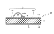
- FIG. 3 is a schematic sectional view of a chip-on submount according to an embodiment of the present invention.
- FIG. 4 is a graph showing the relative value of the optical output in the semiconductor laser device of the example according to the embodiment of the present invention and the comparative example of the prior art.
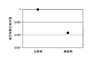
- FIG. 5 is a graph showing the relative value of the forward voltage in the semiconductor laser devices of the example according to the embodiment of the present invention and the comparative example according to the related art.
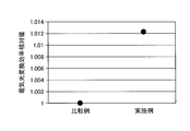
- FIG. 6 is a graph showing relative values of electro-optical conversion efficiencies in semiconductor laser devices of an example according to an embodiment of the present invention and a comparative example according to the related art.
- a high-power multi-mode semiconductor laser device generally has an n-side electrode on the back side of the substrate and a p-side electrode on the front side of the semiconductor laminated film, and is die-bonded to the submount in a junction-down state. Done. Therefore, the p-side electrode exists in the heat radiation path of the semiconductor laser device.
- the present inventor paid attention to the operation of the semiconductor laser device in the junction down state, and examined the contribution of the thermal resistance of the material forming the p-side electrode for heat dissipation.
- a Ti/Pt/Au laminated film is generally used. Since the first Ti layer in the p-side electrode is a layer that contacts the p-type semiconductor layer, it functions as a layer that maintains low contact resistance while having adhesion to the p-type semiconductor layer.
- the second Pt layer has a work function larger than that of the Ti layer and has a function of realizing a low contact resistivity with respect to the p-type semiconductor layer.
- the second Pt layer and the third Au layer react with gallium arsenide (GaAs) used as a p-type semiconductor layer. Therefore, the Ti layer of the first layer functions as a barrier metal that suppresses the diffusion of the Pt layer of the second layer into the GaAs layer, and the Pt layer of the second layer extends to the GaAs layer of the Au layer of the third layer. It functions as a barrier metal that suppresses diffusion.
- Table 1 shows the thermal conductivity (W/m ⁇ K) and the electrical resistivity (n ⁇ m) at room temperature of the metal used for the p-side electrode configured as described above.
- the thickness of the electrode was extremely small compared to the thickness of the semiconductor layer or the submount, the thermal conductivity and thermal resistance of the material forming the electrode were not considered. Further, since the p-side electrode of the semiconductor laser device is used for passing a current flowing through the active layer, thinning the Ti layer or Pt layer functioning as a barrier metal may cause deterioration of reliability. Was considered large. Therefore, regarding the design of the electrode, only the electric resistance of the p-side electrode has been focused and studied.
- the inventor of the present invention shows from Table 1 that the thermal conductivity of the Ti layer and the Pt layer is lower than that of the Au layer by about one digit, specifically, the thickness of the thin Ti/Pt layer is of the order of several tens nm.
- n the number of each layer of the first layer, the second layer, and the third layer constituting the p-side electrode 5
- k n thermal conductivity of each layer
- w c current at which the p-side electrode 5 contacts the p-type semiconductor layer
- Injection width L c : current injection length at which the p-side electrode 5 contacts the p-type semiconductor layer.
- the thermal resistance value R T (K/W ⁇ m 2 ) per unit area of the p-side electrode in the portion in contact with the p-type semiconductor layer, specifically, the Ti layer of the Ti/Pt laminated film is 1
- WPE current conversion efficiency
- FIG. 1 is a sectional view schematically showing the configuration of the semiconductor laser device according to the present embodiment.
- the width direction is a horizontal direction orthogonal to the emission direction and is the X-axis direction in the drawing.
- the Y-axis direction in the figure is the stacking direction of the semiconductor layers in the semiconductor laser device 1.
- the semiconductor laser device 1 configured to be capable of emitting laser light has a wide waveguide stripe width of, for example, 100 ⁇ m or more, a waveguide mode in the horizontal and horizontal multimode, and a driving method of, for example, high continuous wave operation. It is an output semiconductor laser device.
- the high output means an output of about 3 W to 20 W as the output of the semiconductor laser device 1 and about several tens to 200 W as the output of the semiconductor laser device (both at room temperature and CW (Continuous wave) drive). is there.
- the driving method of the semiconductor laser device 1 is a pulse operation
- the laser light emitted from the semiconductor laser device 1 is a pulse laser light having a pulse width of microseconds or more.
- the current injection region R 2 is formed on the waveguide region R 1 .
- the current injection region R 2 is a region to which an electrode according to an embodiment of the present invention is attached and which is used to inject a current into the waveguide region R 1 .
- the semiconductor laser device 1 is, for example, a semiconductor laser device having a ridge structure.
- the horizontal width (waveguide width (stripe width) in the drawing) of the waveguide region in the laser element having the ridge structure is the width in the X direction of the ridge structure provided immediately below the opening A.
- the width of the current injection region in the horizontal direction is the width of the opening A in the X direction.
- the semiconductor laser device 1 has, for example, a p-side electrode 5 as an upper electrode, an n-side electrode 6 as a lower electrode formed on the lower surface, a substrate 7 made of n-type GaAs, and a substrate 7 on the substrate 7.
- the semiconductor laminated part 2 and the passivation film 15 are provided.
- the semiconductor laminated portion 2 includes an n-type buffer layer 8, an n-type clad layer 9, an n-type guide layer 10, an active layer 11, a p-type guide layer 12, a p-type clad layer 13, and a p-type clad layer 13, which are sequentially formed on a substrate 7.
- a mold contact layer 14 is included.
- the n-type buffer layer 8 is made of GaAs and is a buffer layer for growing a laminated structure of high-quality epitaxial layers on the substrate 7.
- the n-type cladding layer 9 and the n-type guide layer 10 are made of AlGaAs whose refractive index and thickness are set so as to realize a desired optical confinement state in the stacking direction.
- the Al composition of the n-type guide layer 10 is, for example, 15% or more and less than 40%.
- the n-type cladding layer 9 has a smaller refractive index than the n-type guide layer 10.
- the thickness of the n-type guide layer 10 is preferably 50 nm or more, for example, about 1000 nm.
- the thickness of the n-type cladding layer 9 is preferably about 1 ⁇ m to 3 ⁇ m.
- these n-type semiconductor layers include, for example, silicon (Si) as an n-type dopant.
- the active layer 11 includes a lower barrier layer, a quantum well layer, and an upper barrier layer, and has a single quantum well (SQW) structure.
- the lower barrier layer and the upper barrier layer have a function of a barrier for confining carriers in the quantum well layer and are made of high-purity AlGaAs that is not intentionally doped.
- the quantum well layer is made of high-purity InGaAs that is not intentionally doped.
- the In composition and film thickness of the quantum well layer and the compositions of the lower barrier layer and the upper barrier layer are set according to the desired emission center wavelength (for example, 900 nm to 1080 nm).
- the structure of the active layer 11 may be a multiple quantum well (MQW) structure in which a desired number of laminated structures of a quantum well layer and barrier layers formed above and below it are repeated, or a single quantum well structure. Further, in the above-mentioned active layer 11, the configuration of the high-purity layer in which doping is not intentionally performed has been described, but a donor or an acceptor may be intentionally added to the quantum well layer, the lower barrier layer, and the upper barrier layer. ..
- MQW multiple quantum well
- the p-type guide layer 12 and the p-type clad layer 13 are paired with the n-type clad layer 9 and the n-type guide layer 10 described above, and have a refractive index and a thickness which are equal to each other so as to realize a desired optical confinement state in the stacking direction.
- a refractive index and a thickness which are equal to each other so as to realize a desired optical confinement state in the stacking direction.
- AlGaAs in which is set.
- the light of the semiconductor laser device 1 mainly exists in the regions of the n-type guide layer 10, the active layer 11, and the p-type guide layer 12 in the Y-axis direction which is the stacking direction.
- the n-type guide layer 10, the active layer 11, and the p-type guide layer 12 are collectively referred to as a waveguide layer.
- the Al composition of the p-type guide layer 12 is, for example, 15% or more and less than 40%.
- the p-type cladding layer 13 has a smaller refractive index than the p-type guide layer 12.
- the Al composition of the p-type cladding layer 13 is set to be slightly larger than that of the n-type cladding layer 9 in order to shift the light field in the layer toward the n-type cladding layer 9 to reduce the waveguide loss.
- the Al composition of the p-type guide layer 12 is set smaller than the Al composition of the p-type cladding layer 13.
- the thickness of the p-type guide layer 12 is preferably 50 nm or more, for example, about 1000 nm.
- the thickness of the p-type cladding layer 13 is preferably about 1 ⁇ m to 3 ⁇ m. Further, these p-type semiconductor layers contain carbon (C) as a p-type dopant.
- the C concentration of the p-type guide layer 12 is set to, for example, 0.1 to 1.0 ⁇ 10 17 cm ⁇ 3 , and preferably 0.5 to 1.0 ⁇ 10 17 cm ⁇ 3 .
- the C concentration of the p-type cladding layer 13 is set to, for example, 1.0 ⁇ 10 17 cm ⁇ 3 or more.
- the p-type dopant may be a group II element such as zinc (Zn), magnesium (Mg), cadmium (Cd), and beryllium (Be).
- the p-type contact layer 14 as a p-type semiconductor layer is a III-V group compound semiconductor layer, specifically, a GaAs layer doped with Zn or C at a concentration higher than 1 ⁇ 10 19 cm ⁇ 3 .
- the passivation film 15 is an insulating film made of SiN x , for example, and has an opening A. Further, in the semiconductor laser device 1 having the ridge structure, the ridge structure for confining the laser light in the X-axis direction is formed in at least a part of the p-type cladding layer 13 immediately below the opening A.
- the p-side electrode 5 is provided on the passivation film 15 so as to cover the opening A.
- the p-side electrode 5 is electrically connected to the p-type contact layer 14 through the opening A.
- the p-side electrode 5 has a Ti/Pt layer having a laminated structure in which a titanium (Ti) layer and a platinum (Pt) layer are sequentially laminated on the surface of the p-type contact layer 14. Since the Ti layer in the p-side electrode 5 has relatively low reactivity with GaAs forming the p-type contact layer 14, the p-type contact layer 14 and the Ti layer have low ohmic contact via a thin interface reaction layer.
- the Ti layer functions as a barrier metal for the Pt layer.
- the p-side electrode 5 is composed of a Ti/Pt/Au layer in which a gold (Au) layer is further laminated on the Ti/Pt layer.
- Au is preferable as the material of the electrode of the semiconductor element because it has high thermal conductivity and low electric resistivity.
- Au diffuses into the semiconductor layer, the reliability of the semiconductor element is lowered, so that the Pt layer is provided as a barrier metal in the lower layer.
- the n-side electrode 6 is composed of an electrode made of a material containing germanium (Ge) such as AuGeNi system.
- Ge germanium
- the p-side electrode 5 is formed by, for example, a vacuum vapor deposition method, a sputtering method, or the like, but a heat treatment at 300° C. to 450° C. is performed after forming the p-side electrode 5.
- the concentration of the p-type impurity doped in the p-type contact layer 14 is preferably higher than 1 ⁇ 10 19 cm ⁇ 3 as described above.
- the thermal resistance is 1.2 ⁇ 10 4 K/W ⁇ m 2 or less at the contact portion where the p-side electrode 5 and the surface of the p-type contact layer 14 contact each other through the opening A.
- the thickness of the Ti/Pt layer is 70 nm or less.
- the thickness of the Ti layer is more preferably 5 nm or more and 35 nm or less.
- a thin interface reaction layer (not shown) is formed at the interface between the p-type contact layer 14 made of GaAs and the first Ti layer of the p-side electrode 5 by the heat treatment process for the n-side electrode 6 described above.
- the film thickness of the Ti layer is defined as the total film thickness of the interface reaction layer containing Ti in the GaAs layer forming the p-type contact layer 14 and the Ti layer.
- the film thickness of the Ti layer and the Pt layer is a film obtained by combining the cross section with a scanning transmission electron microscope (STEM: Scanning Transmission Electron Microscope) and an energy dispersive X-ray spectroscopy (EDS) method. It can be measured by analyzing the thickness and constituent elements.
- STEM scanning transmission electron microscope
- EDS energy dispersive X-ray spectroscopy
- the line profile along the film forming direction of Ga, Ti, Pt, and Au which are the constituent elements of the p-side electrode 5 and the p-type contact layer 14 is measured. After that, each line profile is standardized by the maximum value of the EDS intensity, and the line profile of the standardized EDS intensity of each constituent element is superimposed.
- the distance between the intersection of the Ga and Ti line profiles and the intersection of the Ti and Pt line profiles is defined as the thickness of the Ti layer.
- the distance between the intersection of the line profiles of Ti and Pt and the intersection of the line profiles of Pt and Au is defined as the film thickness of the Pt layer.
- FIG. 2 is a Pt—Ti phase diagram showing the state of formation of an alloy of Pt and Ti. As shown in FIG.
- the intermetallic compounds which have poor reactivity in the heat treatment at a relatively low temperature of 600° C. or less, may be formed by TiPt 8 , TiPt 3 , Ti 3 Pt, and ⁇ -. TiPt.
- the formation of intermetallic compounds of TiPt 8 , TiPt 3 , and Ti 3 Pt must be avoided because the bond structure is complicated. Therefore, from the Pt—Ti phase diagram shown in FIG. 2, the Pt content is preferably 47 to 54% with respect to the Ti content.
- the volume per 1mol of Ti and Pt, respectively is 10.64cm 3 / mol and 9.09cm 3 / mol. Therefore, the thickness of the Pt layer with respect to the thickness of the Ti layer of the p-side electrode 5 is preferably 0.7 times or more and 1 time or less.
- FIG. 3 is a sectional view showing the chip-on submount according to the present embodiment.
- the chip-on submount 20 is a semiconductor element mounting submount including the submount 21 and the semiconductor laser element 1 mounted on the submount 21.
- the submount 21 as a mount includes a substrate 22, a first coating layer 23, and a second coating layer 24.
- the substrate 22 is, for example, aluminum nitride (AlN), alumina (Al 2 O 3 ), beryllia (BeO), boron nitride (BN), diamond, silicon carbide (SiC), silicon nitride (Si 3 N 4 ), silicon dioxide. (SiO 2 ) and zirconia (ZrO 2 ) can be included.
- the substrate 22 is made of AlN, for example.
- the thickness of the substrate 22 is, for example, about 0.3 to 1.0 mm.
- the first coating layer 23 has a thickness in the range of 20 to 200 ⁇ m and is formed on the first surface 22 a of the substrate 22.
- the first surface 22a is a surface on which the semiconductor laser device 1 is mounted in this embodiment.
- the first coating layer 23 includes a coating layer 23a and a coating layer 23b. Both the coating layer 23a and the coating layer 23b are made of, for example, a metal multilayer film containing Cu as a main component.
- the coating layer 23a and the coating layer 23b are separated by a groove 25.
- the groove 25 is provided to electrically insulate the coating layer 23a and the coating layer 23b.
- the semiconductor laser device 1 is bonded and mounted on the submount 21 by AuSn solder via the coating layer 23a.
- a precoat (not shown) made of AuSn is formed on the surface of the coating layer 23a. This facilitates the joint mounting with AuSn solder on the coating layer 23a of the semiconductor laser device 1.
- the p-side electrode 5 is located on the submount 21 side with respect to the submount 21, and the n-side electrode 6 including the substrate 7 is located on the opposite side to the submount 21.
- the active layer 11 is fixed in a junction down state close to the submount 21 side. As a result, the heat generated in the active layer 11 of the semiconductor laser device 1 is easily dissipated through the submount 21.
- the coating layer 23b is electrically connected to the n-side electrode 6 on the upper surface of the semiconductor laser device 1 by the bonding wire 26.
- the semiconductor laser device 1 is configured to be able to supply electric power from the outside via the coating layer 23b, the bonding wire 26, the n-side electrode 6, the p-side electrode 5, and the coating layer 23a.
- the second coating layer 24 has a thickness in the range of 20 to 200 ⁇ m and the same thickness as the first coating layer 23, and is formed on the second surface 22b of the substrate 22.
- the second surface 22b is a surface located on the opposite side of the first surface 22a.
- the second coating layer 24 is made of the same metal multilayer film containing Cu as the main component as the first coating layer 23.
- the structure of the p-side electrode 5 and the semiconductor laser device 1 according to the example based on the above-described embodiment is the structure shown in FIG. 1, and the respective film thicknesses of the Ti/Pt/Au layers are set to those of the related art.
- a description will be given of the p-side electrode 5 according to the comparative example having the film thickness according to.
- the electrode structure, the electrode thickness, the calculated thermal resistance value R T , the thermal resistance value per unit area R T /S, the thermal resistance value R T of the entire semiconductor laser device 1 , LD are shown in Table 2.
- the thickness of the Ti layer is 30 nm
- the thickness of the Pt layer is 30 nm
- the thickness of the Au layer is 100 nm.
- the thickness of the Ti layer is 45 nm
- the thickness of the Pt layer is 100 nm
- the thickness of the Au layer is 100 nm.
- the reference area of the thermal resistance value R T /S per unit area is the area of the contact portion between the p-side electrode 5 and the p-type contact layer 14, that is, the opening area of the opening A, and the current injection width w It is represented by the product of c and the current injection length L c .
- the overall thermal resistance value R T,LD of the semiconductor laser device 1 is the bias current-bias voltage (IV) characteristic and the bias current-laser light output (IL) in the state of the chip-on submount 20. It is a value derived from the characteristics and the current dependence of the oscillation wavelength.
- the thermal resistance value R T according to the example is halved from 8 ⁇ 10 ⁇ 3 K/W to 4 ⁇ 10 ⁇ 3 K/W as compared with the thermal resistance value R T according to the comparative example.
- the thermal resistance value R T /S per unit area in this case is 1.2 ⁇ 10 4 K/W ⁇ m 2 .
- the thermal resistance value R T,LD of the entire semiconductor laser device 1 is reduced by 0.32 K/W in the example as compared with the comparative example.
- the thermal resistance value R T,LD of the entire semiconductor laser device 1 is reduced in the order of 10 ⁇ 1 K/W (100 mK/W) of about 0.32 K/W, and the entire semiconductor laser device 1 is reduced. It can be seen that the thermal resistance value R T,LD of is improved by about two orders of magnitude with respect to the reduction of the thermal resistance value R T of the p-side electrode 5.
- the Ti layer and the Pt layer in the p-side electrode 5 are calculated by making them thinner than the conventional one so that the thermal resistance value per unit area is 1.2 ⁇ 10 4 K/W ⁇ m 2 or less. It can be seen that the actual semiconductor laser device 1 has an effect of improving the thermal resistance by about 80 times compared with the thermal resistance value. This is because the thermal resistance is improved above the calculated value by suppressing the interfacial reaction layer and the intermetallic compound formed by the heat treatment performed after forming the p-side electrode 5, and the forward voltage is further reduced. it is conceivable that.
- the adhesion is about the same in the comparative example and the example. It was also confirmed that the peeling of the p-side electrode 5 did not occur when the resist was lifted off during the formation of the electrode pattern. Further, even if the Ti layer is thinned and the Pt layer as the second layer is thinned from 100 nm in the comparative example to 30 nm in the example, no difference in reliability in the aging test is observed between the example and the comparative example.
- the line profiles of the constituent elements Ga, As, Ti, Pt, and Au were measured by the STEM-EDS method.
- a thin interface reaction layer having a film thickness of about 5 nm in which Ga, As, and Ti were mixed was observed between the GaAs layer, which is the p-type contact layer, and the Ti layer. Therefore, the thickness of the Ti layer that is the first layer is preferably 5 nm or more. Further, considering the effect of improving WPE due to the improvement of thermal resistance and the film thickness variation of the Ti layer of about 5 nm at the time of forming the Ti layer as the first layer, it has been clarified that the range of 35 nm or less is preferable. ..
- the film thickness of the Pt layer that is the second layer is less than 30 nm, the Pt layer does not function as a barrier metal for the Au layer. Accordingly, the film thickness of the Pt layer that is the second layer is preferably 30 nm or more. From the viewpoint of thermal resistance, it is preferable that the total thickness of the first Ti layer and the second Pt layer is smaller. However, considering the film thickness variation of about 5 nm when forming the Pt layer, the film thickness of the second Pt layer is preferably in the range of 30 nm to 35 nm.
- the total thickness of the Ti layer as the first layer and the Pt layer as the second layer is preferably 70 nm or less.
- the Au layer which is the third layer, is superior to other metals in terms of thermal resistance and electric resistance, and is therefore the most suitable electrode material for high-power semiconductor laser devices.
- the material of the third layer is not limited to Au, and a multi-layer metal laminated structure or the like may be adopted.
- FIG. 4, FIG. 5, and FIG. 6 show the relative values of the optical output, the relative value of the forward voltage, and the relative electro-optical conversion efficiency in the semiconductor laser device 1 of the example according to the embodiment and the comparative example of the related art, respectively. It is a graph which shows a value. 4 to 6, the relative value of the example is a relative value standardized with all of the light output, forward voltage, and electro-optical conversion efficiency in the comparative example according to the related art.
- the optical output of the semiconductor laser device according to the example increased by about 1.1% as compared with the comparative example. It is considered that this is because the junction temperature decreased as the thermal resistance of the p-side electrode 5 decreased. It can be seen from FIG. 5 that the forward voltage of the semiconductor laser device according to the example is reduced by about 0.2% as compared with the comparative example. This is because the electrode material of the p-side electrode 5 was the same in the example and the comparative example, so that the thickness of the p-side electrode 5 was reduced, and the formation of the interface reaction layer and the intermetallic compound was suppressed. It is considered that this is because the electrical resistance was reduced. It can be seen from FIG.
- the WPE of the semiconductor laser device according to the example increased by about 1.2% as compared with the comparative example. It is considered that this is due to not only the increase in light output but also the decrease in forward voltage. From these results, it is understood that the junction temperature is lowered by lowering the thermal resistance of the p-side electrode 5, the light output can be increased, and the WPE can be improved.
- the Ti/Pt layer in the p-side electrode 5, which is the p-side electrode of the semiconductor laser device, is made thinner than in the past, and the thermal resistance value per unit area is 1.2.
- the WPE of the semiconductor laser device 1 can be improved by controlling the density to be not more than ⁇ 10 4 K/W ⁇ m 2 .
- the present invention has been specifically described above, but the present invention is not limited to the above-described embodiment, and various modifications can be made based on the technical idea of the present invention.
- the numerical values and the configuration of the semiconductor laser device described in the above-described embodiment are merely examples, and different numerical values and configurations may be used if necessary.
- the present invention can be preferably used for industrial lasers with high output and high efficiency.
Landscapes
- Physics & Mathematics (AREA)
- Condensed Matter Physics & Semiconductors (AREA)
- General Physics & Mathematics (AREA)
- Electromagnetism (AREA)
- Optics & Photonics (AREA)
- Geometry (AREA)
- Semiconductor Lasers (AREA)
Abstract
Description

RT=Σn=1~3dn/(kn・wc・Lc)…(1)
n:p側電極5を構成する第1層、第2層、第3層の各層の番号、kn:各層の熱伝導率、wc:p側電極5がp型半導体層と接触する電流注入幅、Lc:p側電極5がp型半導体層と接触する電流注入長。半導体レーザ素子の構造においては、半導体層に対する電流の注入領域を制限する非注入領域を設けることから、電流注入幅wcは導波路のストライプ幅より小さくなり、p側電極5の電流注入長Lcは半導体レーザ素子1の共振器長より小さくなる。
次に、上述した本発明者の鋭意検討に基づく、本発明の一実施形態による電極を備えた半導体レーザ素子について説明する。図1は、本実施形態による半導体レーザ素子の構成を概略的に示す断面図である。なお、図1において、幅方向とは、出射方向に直交する水平方向であって図中X軸方向である。図中Y軸方向は、半導体レーザ素子1における半導体層の積層方向である。
次に、一実施形態によるチップオンサブマウントについて説明する。図3は、本実施形態によるチップオンサブマウントを示す断面図である。図3に示すように、チップオンサブマウント20は、サブマウント21、およびサブマウント21に実装された半導体レーザ素子1を備えて構成される半導体素子搭載サブマウントである。
次に、上述した一実施形態に基づく実施例によるp側電極5、および半導体レーザ素子1の構造は図1に示す構造であって、Ti/Pt/Au層のそれぞれの膜厚を、従来技術による膜厚とした比較例によるp側電極5について説明する。実施例および比較例によるp側電極5における、電極構造、電極厚さ、計算による熱抵抗値RT、単位面積当たりの熱抵抗値RT/S、半導体レーザ素子1全体の熱抵抗値RT,LDを、表2に示す。表2に示すように、実施例によるp側電極5は、Ti層の膜厚を30nm、Pt層の膜厚を30nm、Au層の膜厚を100nmとする。これに対し、比較例による電極は、Ti層の膜厚を45nm、Pt層の膜厚を100nm、Au層の膜厚を100nmとする。なお、単位面積当たりの熱抵抗値RT/Sにおける基準となる面積は、p側電極5とp型コンタクト層14との接触部分の面積、すなわち開口部Aの開口面積となり、電流注入幅wcと電流注入長Lcとの積で表される。また、半導体レーザ素子1の全体の熱抵抗値RT,LDは、チップオンサブマウント20の状態で、バイアス電流-バイアス電圧(I-V)特性およびバイアス電流-レーザ光出力(I-L)特性と、発振波長の電流依存性から導出した値である。

2 半導体積層部
5 p側電極
6 n側電極
7 基板
8 n型バッファ層
9 n型クラッド層
10 n型ガイド層
11 活性層
12 p型ガイド層
13 p型クラッド層
14 p型コンタクト層
15 パッシベーション膜
20 チップオンサブマウント
21 サブマウント
22 基板
22a 第一表面
22b 第二表面
23 第一被覆層
23a,23b 被覆層
24 第二被覆層
25 溝
26 ボンディングワイヤ
Claims (14)
- p型半導体層の表面にTi層およびPt層が順次積層されて構成された電極であって、
前記p型半導体層の表面との接触部分における単位面積当たりの熱抵抗が、1.2×10⁴K/W・m2以下である
ことを特徴とする電極。 - 前記Ti層の膜厚は35nm以下である
ことを特徴とする請求項1に記載の電極。 - 前記Ti層の膜厚は5nm以上35nm以下である
ことを特徴とする請求項1または2に記載の電極。 - 前記Ti層の膜厚と前記Pt層の膜厚との合計は70nm以下である
ことを特徴とする請求項1~3のいずれか1項に記載の電極。 - 前記Pt層の膜厚は30nm以上である
ことを特徴とする請求項1~4のいずれか1項に記載の電極。 - 前記Pt層の膜厚は、前記Ti層の膜厚に対して0.7倍以上1倍以下である
ことを特徴とする請求項1~5のいずれか1項に記載の電極。 - 前記Pt層の上層にAu層が積層されている
ことを特徴とする請求項1~6のいずれか1項に記載の電極。 - n型半導体層、活性層、およびp型半導体層が順次積層され、レーザ光を出射可能に構成された半導体レーザ素子であって、
前記p型半導体層の表面に、請求項1~7のいずれか1項に記載の電極が設けられている
ことを特徴とする半導体レーザ素子。 - 前記p型半導体層がIII-V族化合物半導体層である
ことを特徴とする請求項8に記載の半導体レーザ素子。 - 前記p型半導体層がGaAs層である
ことを特徴とする請求項8または9に記載の半導体レーザ素子。 - 前記p型半導体層におけるp型不純物濃度が、1×1019cm-3以上である
ことを特徴とする請求項8~10のいずれか1項に記載の半導体レーザ素子。 - 前記半導体レーザ素子における駆動方法が連続波動作である
ことを特徴とする請求項8~11のいずれか1項に記載の半導体レーザ素子。 - ストライプ幅が100μm以上である
ことを特徴とする請求項8~12のいずれか1項に記載の半導体レーザ素子。 - 請求項8~13のいずれか1項に記載の半導体レーザ素子と、
前記半導体レーザ素子をジャンクションダウンの状態で固定するマウントと、を備える
ことを特徴とするチップオンサブマウント。
Priority Applications (4)
| Application Number | Priority Date | Filing Date | Title |
|---|---|---|---|
| CN202080013968.1A CN113424380B (zh) | 2019-02-13 | 2020-02-06 | 电极、半导体激光元件以及带有芯片的辅助固定件 |
| EP20756057.4A EP3926768B1 (en) | 2019-02-13 | 2020-02-06 | Electrode, semiconductor laser element, and chip on submount |
| JP2020572207A JP7470649B2 (ja) | 2019-02-13 | 2020-02-06 | 半導体レーザ素子およびチップオンサブマウント |
| US17/394,978 US20210367400A1 (en) | 2019-02-13 | 2021-08-05 | Electrode, semiconductor laser element, and chip-on-submount |
Applications Claiming Priority (2)
| Application Number | Priority Date | Filing Date | Title |
|---|---|---|---|
| JP2019023288 | 2019-02-13 | ||
| JP2019-023288 | 2019-02-13 |
Related Child Applications (1)
| Application Number | Title | Priority Date | Filing Date |
|---|---|---|---|
| US17/394,978 Continuation US20210367400A1 (en) | 2019-02-13 | 2021-08-05 | Electrode, semiconductor laser element, and chip-on-submount |
Publications (1)
| Publication Number | Publication Date |
|---|---|
| WO2020166483A1 true WO2020166483A1 (ja) | 2020-08-20 |
Family
ID=72045371
Family Applications (1)
| Application Number | Title | Priority Date | Filing Date |
|---|---|---|---|
| PCT/JP2020/004604 Ceased WO2020166483A1 (ja) | 2019-02-13 | 2020-02-06 | 電極、半導体レーザ素子、およびチップオンサブマウント |
Country Status (5)
| Country | Link |
|---|---|
| US (1) | US20210367400A1 (ja) |
| EP (1) | EP3926768B1 (ja) |
| JP (1) | JP7470649B2 (ja) |
| CN (1) | CN113424380B (ja) |
| WO (1) | WO2020166483A1 (ja) |
Citations (7)
| Publication number | Priority date | Publication date | Assignee | Title |
|---|---|---|---|---|
| JP3314616B2 (ja) | 1995-10-05 | 2002-08-12 | 株式会社デンソー | 大出力用半導体レーザ素子 |
| US20040013147A1 (en) * | 2002-04-03 | 2004-01-22 | Manuela Buda | Low divergence diode laser |
| JP2006156639A (ja) * | 2004-11-29 | 2006-06-15 | Sharp Corp | 半導体レーザ素子、光ディスク装置および光伝送システム |
| JP2013062315A (ja) * | 2011-09-12 | 2013-04-04 | Sumitomo Electric Ind Ltd | Iii族窒化物半導体レーザ、レーザ装置、及びiii族窒化物半導体レーザを製造する方法 |
| JP2013125886A (ja) * | 2011-12-15 | 2013-06-24 | Sony Corp | 半導体レーザ素子及び半導体レーザ素子の製造方法 |
| WO2014018599A1 (en) * | 2012-07-24 | 2014-01-30 | Board Of Regents, The University Of Texas System | Terahertz quantum cascade laser with difference-frequency generation |
| JP2018037601A (ja) * | 2016-09-02 | 2018-03-08 | 株式会社リコー | 積層体、発光装置、光源ユニット、レーザ装置、点火装置 |
Family Cites Families (9)
| Publication number | Priority date | Publication date | Assignee | Title |
|---|---|---|---|---|
| JP4018177B2 (ja) * | 1996-09-06 | 2007-12-05 | 株式会社東芝 | 窒化ガリウム系化合物半導体発光素子 |
| EP0843393B1 (en) * | 1996-11-18 | 2003-10-15 | Mitsubishi Chemical Corporation | Semiconductor laser diode |
| JP3292193B2 (ja) * | 1999-01-28 | 2002-06-17 | 日本電気株式会社 | オーミック電極の製造方法及び半導体装置の製造方法 |
| US7558307B2 (en) * | 2004-02-16 | 2009-07-07 | Sharp Kabushiki Kaisha | Semiconductor laser device, semiconductor laser device manufacturing method, optical disk apparatus and optical transmission system |
| JP5540296B2 (ja) * | 2010-10-13 | 2014-07-02 | 独立行政法人産業技術総合研究所 | ダイヤモンド電子素子及びその製造方法 |
| JP6024365B2 (ja) * | 2012-10-09 | 2016-11-16 | 三菱電機株式会社 | 半導体レーザ装置 |
| WO2017098689A1 (ja) * | 2015-12-09 | 2017-06-15 | パナソニック株式会社 | 半導体発光装置 |
| CN118970619B (zh) * | 2017-05-01 | 2025-08-22 | 新唐科技日本株式会社 | 氮化物系发光装置 |
| JP7048875B2 (ja) * | 2017-08-30 | 2022-04-06 | 日亜化学工業株式会社 | 発光装置の製造方法 |
-
2020
- 2020-02-06 JP JP2020572207A patent/JP7470649B2/ja not_active Ceased
- 2020-02-06 WO PCT/JP2020/004604 patent/WO2020166483A1/ja not_active Ceased
- 2020-02-06 CN CN202080013968.1A patent/CN113424380B/zh active Active
- 2020-02-06 EP EP20756057.4A patent/EP3926768B1/en active Active
-
2021
- 2021-08-05 US US17/394,978 patent/US20210367400A1/en not_active Abandoned
Patent Citations (7)
| Publication number | Priority date | Publication date | Assignee | Title |
|---|---|---|---|---|
| JP3314616B2 (ja) | 1995-10-05 | 2002-08-12 | 株式会社デンソー | 大出力用半導体レーザ素子 |
| US20040013147A1 (en) * | 2002-04-03 | 2004-01-22 | Manuela Buda | Low divergence diode laser |
| JP2006156639A (ja) * | 2004-11-29 | 2006-06-15 | Sharp Corp | 半導体レーザ素子、光ディスク装置および光伝送システム |
| JP2013062315A (ja) * | 2011-09-12 | 2013-04-04 | Sumitomo Electric Ind Ltd | Iii族窒化物半導体レーザ、レーザ装置、及びiii族窒化物半導体レーザを製造する方法 |
| JP2013125886A (ja) * | 2011-12-15 | 2013-06-24 | Sony Corp | 半導体レーザ素子及び半導体レーザ素子の製造方法 |
| WO2014018599A1 (en) * | 2012-07-24 | 2014-01-30 | Board Of Regents, The University Of Texas System | Terahertz quantum cascade laser with difference-frequency generation |
| JP2018037601A (ja) * | 2016-09-02 | 2018-03-08 | 株式会社リコー | 積層体、発光装置、光源ユニット、レーザ装置、点火装置 |
Non-Patent Citations (1)
| Title |
|---|
| See also references of EP3926768A4 |
Also Published As
| Publication number | Publication date |
|---|---|
| JP7470649B2 (ja) | 2024-04-18 |
| CN113424380A (zh) | 2021-09-21 |
| EP3926768B1 (en) | 2025-05-14 |
| EP3926768A4 (en) | 2023-01-04 |
| JPWO2020166483A1 (ja) | 2021-12-16 |
| US20210367400A1 (en) | 2021-11-25 |
| CN113424380B (zh) | 2024-03-08 |
| EP3926768A1 (en) | 2021-12-22 |
Similar Documents
| Publication | Publication Date | Title |
|---|---|---|
| US9722394B2 (en) | Semiconductor laser diode | |
| US6777792B2 (en) | Semiconductor device and package with high heat radiation effect | |
| CN1534841B (zh) | 半导体激光器元件及其制造方法 | |
| US6791181B2 (en) | Semiconductor light emitting device | |
| JPH07105572B2 (ja) | 電気励起キャビティ・レーザ装置 | |
| JP2010118702A (ja) | 窒化物半導体発光素子 | |
| US9331453B2 (en) | Laser diode device | |
| US6873634B2 (en) | Semiconductor laser diode | |
| CN101656399B (zh) | 多束激光二极管 | |
| US9008138B2 (en) | Laser diode device | |
| JP5877070B2 (ja) | 半導体レーザ装置 | |
| US8989228B2 (en) | Laser diode device, method of driving the same, and laser diode apparatus | |
| JP2004349595A (ja) | 窒化物半導体レーザ装置およびその製造方法 | |
| JP7470649B2 (ja) | 半導体レーザ素子およびチップオンサブマウント | |
| EP3754799B1 (en) | Optical semiconductor device | |
| US20050152419A1 (en) | Semiconductor laser element, manufacturing method thereof, optical disk apparatus and optical transmission system | |
| US20040013149A1 (en) | Nitride semiconductor laser device chip and laser apparatus including the same | |
| JPH10303493A (ja) | 窒化物半導体レーザ素子 | |
| JP2022020503A (ja) | 半導体レーザおよび半導体レーザ装置 | |
| JP2019207966A (ja) | 半導体発光素子 | |
| JP2007049088A (ja) | 高出力赤色半導体レーザ | |
| CN118575377A (zh) | 半导体激光装置及半导体激光元件的制造方法 | |
| JP2010272784A (ja) | 半導体レーザ装置 | |
| JP2008130665A (ja) | 半導体発光素子およびその製造方法、並びに発光装置 | |
| JP2008130664A (ja) | 半導体発光素子および発光装置 |
Legal Events
| Date | Code | Title | Description |
|---|---|---|---|
| 121 | Ep: the epo has been informed by wipo that ep was designated in this application |
Ref document number: 20756057 Country of ref document: EP Kind code of ref document: A1 |
|
| ENP | Entry into the national phase |
Ref document number: 2020572207 Country of ref document: JP Kind code of ref document: A |
|
| NENP | Non-entry into the national phase |
Ref country code: DE |
|
| ENP | Entry into the national phase |
Ref document number: 2020756057 Country of ref document: EP Effective date: 20210913 |
|
| WWG | Wipo information: grant in national office |
Ref document number: 2020756057 Country of ref document: EP |