WO2020170977A1 - 二次元材料積層体の製造方法及び積層体 - Google Patents
二次元材料積層体の製造方法及び積層体 Download PDFInfo
- Publication number
- WO2020170977A1 WO2020170977A1 PCT/JP2020/005841 JP2020005841W WO2020170977A1 WO 2020170977 A1 WO2020170977 A1 WO 2020170977A1 JP 2020005841 W JP2020005841 W JP 2020005841W WO 2020170977 A1 WO2020170977 A1 WO 2020170977A1
- Authority
- WO
- WIPO (PCT)
- Prior art keywords
- pressure
- sensitive adhesive
- laminate
- substrate
- dimensional material
- Prior art date
- Legal status (The legal status is an assumption and is not a legal conclusion. Google has not performed a legal analysis and makes no representation as to the accuracy of the status listed.)
- Ceased
Links
Images


Classifications
-
- B—PERFORMING OPERATIONS; TRANSPORTING
- B32—LAYERED PRODUCTS
- B32B—LAYERED PRODUCTS, i.e. PRODUCTS BUILT-UP OF STRATA OF FLAT OR NON-FLAT, e.g. CELLULAR OR HONEYCOMB, FORM
- B32B37/00—Methods or apparatus for laminating, e.g. by curing or by ultrasonic bonding
- B32B37/12—Methods or apparatus for laminating, e.g. by curing or by ultrasonic bonding characterised by using adhesives
-
- H—ELECTRICITY
- H01—ELECTRIC ELEMENTS
- H01B—CABLES; CONDUCTORS; INSULATORS; SELECTION OF MATERIALS FOR THEIR CONDUCTIVE, INSULATING OR DIELECTRIC PROPERTIES
- H01B9/00—Power cables
- H01B9/02—Power cables with screens or conductive layers, e.g. for avoiding large potential gradients
- H01B9/027—Power cables with screens or conductive layers, e.g. for avoiding large potential gradients composed of semi-conducting layers
-
- B—PERFORMING OPERATIONS; TRANSPORTING
- B32—LAYERED PRODUCTS
- B32B—LAYERED PRODUCTS, i.e. PRODUCTS BUILT-UP OF STRATA OF FLAT OR NON-FLAT, e.g. CELLULAR OR HONEYCOMB, FORM
- B32B37/00—Methods or apparatus for laminating, e.g. by curing or by ultrasonic bonding
- B32B37/14—Methods or apparatus for laminating, e.g. by curing or by ultrasonic bonding characterised by the properties of the layers
- B32B37/16—Methods or apparatus for laminating, e.g. by curing or by ultrasonic bonding characterised by the properties of the layers with all layers existing as coherent layers before laminating
-
- B—PERFORMING OPERATIONS; TRANSPORTING
- B32—LAYERED PRODUCTS
- B32B—LAYERED PRODUCTS, i.e. PRODUCTS BUILT-UP OF STRATA OF FLAT OR NON-FLAT, e.g. CELLULAR OR HONEYCOMB, FORM
- B32B37/00—Methods or apparatus for laminating, e.g. by curing or by ultrasonic bonding
- B32B37/14—Methods or apparatus for laminating, e.g. by curing or by ultrasonic bonding characterised by the properties of the layers
- B32B37/26—Methods or apparatus for laminating, e.g. by curing or by ultrasonic bonding characterised by the properties of the layers with at least one layer which influences the bonding during the lamination process, e.g. release layers or pressure equalising layers
-
- B—PERFORMING OPERATIONS; TRANSPORTING
- B32—LAYERED PRODUCTS
- B32B—LAYERED PRODUCTS, i.e. PRODUCTS BUILT-UP OF STRATA OF FLAT OR NON-FLAT, e.g. CELLULAR OR HONEYCOMB, FORM
- B32B7/00—Layered products characterised by the relation between layers; Layered products characterised by the relative orientation of features between layers, or by the relative values of a measurable parameter between layers, i.e. products comprising layers having different physical, chemical or physicochemical properties; Layered products characterised by the interconnection of layers
- B32B7/02—Physical, chemical or physicochemical properties
- B32B7/022—Mechanical properties
-
- B—PERFORMING OPERATIONS; TRANSPORTING
- B32—LAYERED PRODUCTS
- B32B—LAYERED PRODUCTS, i.e. PRODUCTS BUILT-UP OF STRATA OF FLAT OR NON-FLAT, e.g. CELLULAR OR HONEYCOMB, FORM
- B32B7/00—Layered products characterised by the relation between layers; Layered products characterised by the relative orientation of features between layers, or by the relative values of a measurable parameter between layers, i.e. products comprising layers having different physical, chemical or physicochemical properties; Layered products characterised by the interconnection of layers
- B32B7/02—Physical, chemical or physicochemical properties
- B32B7/023—Optical properties
-
- B—PERFORMING OPERATIONS; TRANSPORTING
- B32—LAYERED PRODUCTS
- B32B—LAYERED PRODUCTS, i.e. PRODUCTS BUILT-UP OF STRATA OF FLAT OR NON-FLAT, e.g. CELLULAR OR HONEYCOMB, FORM
- B32B7/00—Layered products characterised by the relation between layers; Layered products characterised by the relative orientation of features between layers, or by the relative values of a measurable parameter between layers, i.e. products comprising layers having different physical, chemical or physicochemical properties; Layered products characterised by the interconnection of layers
- B32B7/02—Physical, chemical or physicochemical properties
- B32B7/025—Electric or magnetic properties
-
- B—PERFORMING OPERATIONS; TRANSPORTING
- B32—LAYERED PRODUCTS
- B32B—LAYERED PRODUCTS, i.e. PRODUCTS BUILT-UP OF STRATA OF FLAT OR NON-FLAT, e.g. CELLULAR OR HONEYCOMB, FORM
- B32B7/00—Layered products characterised by the relation between layers; Layered products characterised by the relative orientation of features between layers, or by the relative values of a measurable parameter between layers, i.e. products comprising layers having different physical, chemical or physicochemical properties; Layered products characterised by the interconnection of layers
- B32B7/02—Physical, chemical or physicochemical properties
- B32B7/027—Thermal properties
-
- B—PERFORMING OPERATIONS; TRANSPORTING
- B32—LAYERED PRODUCTS
- B32B—LAYERED PRODUCTS, i.e. PRODUCTS BUILT-UP OF STRATA OF FLAT OR NON-FLAT, e.g. CELLULAR OR HONEYCOMB, FORM
- B32B7/00—Layered products characterised by the relation between layers; Layered products characterised by the relative orientation of features between layers, or by the relative values of a measurable parameter between layers, i.e. products comprising layers having different physical, chemical or physicochemical properties; Layered products characterised by the interconnection of layers
- B32B7/04—Interconnection of layers
- B32B7/06—Interconnection of layers permitting easy separation
-
- B—PERFORMING OPERATIONS; TRANSPORTING
- B32—LAYERED PRODUCTS
- B32B—LAYERED PRODUCTS, i.e. PRODUCTS BUILT-UP OF STRATA OF FLAT OR NON-FLAT, e.g. CELLULAR OR HONEYCOMB, FORM
- B32B7/00—Layered products characterised by the relation between layers; Layered products characterised by the relative orientation of features between layers, or by the relative values of a measurable parameter between layers, i.e. products comprising layers having different physical, chemical or physicochemical properties; Layered products characterised by the interconnection of layers
- B32B7/04—Interconnection of layers
- B32B7/12—Interconnection of layers using interposed adhesives or interposed materials with bonding properties
-
- B—PERFORMING OPERATIONS; TRANSPORTING
- B32—LAYERED PRODUCTS
- B32B—LAYERED PRODUCTS, i.e. PRODUCTS BUILT-UP OF STRATA OF FLAT OR NON-FLAT, e.g. CELLULAR OR HONEYCOMB, FORM
- B32B9/00—Layered products comprising a layer of a particular substance not covered by groups B32B11/00 - B32B29/00
- B32B9/005—Layered products comprising a layer of a particular substance not covered by groups B32B11/00 - B32B29/00 comprising one layer of ceramic material, e.g. porcelain, ceramic tile
- B32B9/007—Layered products comprising a layer of a particular substance not covered by groups B32B11/00 - B32B29/00 comprising one layer of ceramic material, e.g. porcelain, ceramic tile comprising carbon, e.g. graphite, composite carbon
-
- B—PERFORMING OPERATIONS; TRANSPORTING
- B32—LAYERED PRODUCTS
- B32B—LAYERED PRODUCTS, i.e. PRODUCTS BUILT-UP OF STRATA OF FLAT OR NON-FLAT, e.g. CELLULAR OR HONEYCOMB, FORM
- B32B9/00—Layered products comprising a layer of a particular substance not covered by groups B32B11/00 - B32B29/00
- B32B9/04—Layered products comprising a layer of a particular substance not covered by groups B32B11/00 - B32B29/00 comprising such particular substance as the main or only constituent of a layer, which is next to another layer of the same or of a different material
-
- C—CHEMISTRY; METALLURGY
- C09—DYES; PAINTS; POLISHES; NATURAL RESINS; ADHESIVES; COMPOSITIONS NOT OTHERWISE PROVIDED FOR; APPLICATIONS OF MATERIALS NOT OTHERWISE PROVIDED FOR
- C09J—ADHESIVES; NON-MECHANICAL ASPECTS OF ADHESIVE PROCESSES IN GENERAL; ADHESIVE PROCESSES NOT PROVIDED FOR ELSEWHERE; USE OF MATERIALS AS ADHESIVES
- C09J201/00—Adhesives based on unspecified macromolecular compounds
-
- C—CHEMISTRY; METALLURGY
- C09—DYES; PAINTS; POLISHES; NATURAL RESINS; ADHESIVES; COMPOSITIONS NOT OTHERWISE PROVIDED FOR; APPLICATIONS OF MATERIALS NOT OTHERWISE PROVIDED FOR
- C09J—ADHESIVES; NON-MECHANICAL ASPECTS OF ADHESIVE PROCESSES IN GENERAL; ADHESIVE PROCESSES NOT PROVIDED FOR ELSEWHERE; USE OF MATERIALS AS ADHESIVES
- C09J5/00—Adhesive processes in general; Adhesive processes not provided for elsewhere, e.g. relating to primers
-
- C—CHEMISTRY; METALLURGY
- C09—DYES; PAINTS; POLISHES; NATURAL RESINS; ADHESIVES; COMPOSITIONS NOT OTHERWISE PROVIDED FOR; APPLICATIONS OF MATERIALS NOT OTHERWISE PROVIDED FOR
- C09J—ADHESIVES; NON-MECHANICAL ASPECTS OF ADHESIVE PROCESSES IN GENERAL; ADHESIVE PROCESSES NOT PROVIDED FOR ELSEWHERE; USE OF MATERIALS AS ADHESIVES
- C09J7/00—Adhesives in the form of films or foils
- C09J7/30—Adhesives in the form of films or foils characterised by the adhesive composition
- C09J7/38—Pressure-sensitive adhesives [PSA]
-
- H—ELECTRICITY
- H01—ELECTRIC ELEMENTS
- H01B—CABLES; CONDUCTORS; INSULATORS; SELECTION OF MATERIALS FOR THEIR CONDUCTIVE, INSULATING OR DIELECTRIC PROPERTIES
- H01B13/00—Apparatus or processes specially adapted for manufacturing conductors or cables
- H01B13/0026—Apparatus for manufacturing conducting or semi-conducting layers, e.g. deposition of metal
-
- H—ELECTRICITY
- H01—ELECTRIC ELEMENTS
- H01B—CABLES; CONDUCTORS; INSULATORS; SELECTION OF MATERIALS FOR THEIR CONDUCTIVE, INSULATING OR DIELECTRIC PROPERTIES
- H01B7/00—Insulated conductors or cables characterised by their form
- H01B7/17—Protection against damage caused by external factors, e.g. sheaths or armouring
- H01B7/18—Protection against damage caused by wear, mechanical force or pressure; Sheaths; Armouring
- H01B7/22—Metal wires or tapes, e.g. made of steel
-
- H—ELECTRICITY
- H02—GENERATION; CONVERSION OR DISTRIBUTION OF ELECTRIC POWER
- H02G—INSTALLATION OF ELECTRIC CABLES OR LINES, OR OF COMBINED OPTICAL AND ELECTRIC CABLES OR LINES
- H02G15/00—Cable fittings
- H02G15/08—Cable junctions
- H02G15/10—Cable junctions protected by boxes, e.g. by distribution, connection or junction boxes
-
- B—PERFORMING OPERATIONS; TRANSPORTING
- B32—LAYERED PRODUCTS
- B32B—LAYERED PRODUCTS, i.e. PRODUCTS BUILT-UP OF STRATA OF FLAT OR NON-FLAT, e.g. CELLULAR OR HONEYCOMB, FORM
- B32B37/00—Methods or apparatus for laminating, e.g. by curing or by ultrasonic bonding
- B32B37/12—Methods or apparatus for laminating, e.g. by curing or by ultrasonic bonding characterised by using adhesives
- B32B2037/1253—Methods or apparatus for laminating, e.g. by curing or by ultrasonic bonding characterised by using adhesives curable adhesive
-
- B—PERFORMING OPERATIONS; TRANSPORTING
- B32—LAYERED PRODUCTS
- B32B—LAYERED PRODUCTS, i.e. PRODUCTS BUILT-UP OF STRATA OF FLAT OR NON-FLAT, e.g. CELLULAR OR HONEYCOMB, FORM
- B32B2250/00—Layers arrangement
- B32B2250/02—2 layers
-
- B—PERFORMING OPERATIONS; TRANSPORTING
- B32—LAYERED PRODUCTS
- B32B—LAYERED PRODUCTS, i.e. PRODUCTS BUILT-UP OF STRATA OF FLAT OR NON-FLAT, e.g. CELLULAR OR HONEYCOMB, FORM
- B32B2250/00—Layers arrangement
- B32B2250/03—3 layers
-
- B—PERFORMING OPERATIONS; TRANSPORTING
- B32—LAYERED PRODUCTS
- B32B—LAYERED PRODUCTS, i.e. PRODUCTS BUILT-UP OF STRATA OF FLAT OR NON-FLAT, e.g. CELLULAR OR HONEYCOMB, FORM
- B32B2250/00—Layers arrangement
- B32B2250/04—4 layers
-
- B—PERFORMING OPERATIONS; TRANSPORTING
- B32—LAYERED PRODUCTS
- B32B—LAYERED PRODUCTS, i.e. PRODUCTS BUILT-UP OF STRATA OF FLAT OR NON-FLAT, e.g. CELLULAR OR HONEYCOMB, FORM
- B32B2307/00—Properties of the layers or laminate
- B32B2307/50—Properties of the layers or laminate having particular mechanical properties
- B32B2307/54—Yield strength; Tensile strength
-
- B—PERFORMING OPERATIONS; TRANSPORTING
- B32—LAYERED PRODUCTS
- B32B—LAYERED PRODUCTS, i.e. PRODUCTS BUILT-UP OF STRATA OF FLAT OR NON-FLAT, e.g. CELLULAR OR HONEYCOMB, FORM
- B32B2307/00—Properties of the layers or laminate
- B32B2307/70—Other properties
- B32B2307/748—Releasability
-
- B—PERFORMING OPERATIONS; TRANSPORTING
- B32—LAYERED PRODUCTS
- B32B—LAYERED PRODUCTS, i.e. PRODUCTS BUILT-UP OF STRATA OF FLAT OR NON-FLAT, e.g. CELLULAR OR HONEYCOMB, FORM
- B32B2405/00—Adhesive articles, e.g. adhesive tapes
-
- B—PERFORMING OPERATIONS; TRANSPORTING
- B32—LAYERED PRODUCTS
- B32B—LAYERED PRODUCTS, i.e. PRODUCTS BUILT-UP OF STRATA OF FLAT OR NON-FLAT, e.g. CELLULAR OR HONEYCOMB, FORM
- B32B37/00—Methods or apparatus for laminating, e.g. by curing or by ultrasonic bonding
- B32B37/02—Methods or apparatus for laminating, e.g. by curing or by ultrasonic bonding characterised by a sequence of laminating steps, e.g. by adding new layers at consecutive laminating stations
- B32B37/025—Transfer laminating
-
- C—CHEMISTRY; METALLURGY
- C09—DYES; PAINTS; POLISHES; NATURAL RESINS; ADHESIVES; COMPOSITIONS NOT OTHERWISE PROVIDED FOR; APPLICATIONS OF MATERIALS NOT OTHERWISE PROVIDED FOR
- C09J—ADHESIVES; NON-MECHANICAL ASPECTS OF ADHESIVE PROCESSES IN GENERAL; ADHESIVE PROCESSES NOT PROVIDED FOR ELSEWHERE; USE OF MATERIALS AS ADHESIVES
- C09J2203/00—Applications of adhesives in processes or use of adhesives in the form of films or foils
- C09J2203/326—Applications of adhesives in processes or use of adhesives in the form of films or foils for bonding electronic components such as wafers, chips or semiconductors
-
- C—CHEMISTRY; METALLURGY
- C09—DYES; PAINTS; POLISHES; NATURAL RESINS; ADHESIVES; COMPOSITIONS NOT OTHERWISE PROVIDED FOR; APPLICATIONS OF MATERIALS NOT OTHERWISE PROVIDED FOR
- C09J—ADHESIVES; NON-MECHANICAL ASPECTS OF ADHESIVE PROCESSES IN GENERAL; ADHESIVE PROCESSES NOT PROVIDED FOR ELSEWHERE; USE OF MATERIALS AS ADHESIVES
- C09J2301/00—Additional features of adhesives in the form of films or foils
- C09J2301/40—Additional features of adhesives in the form of films or foils characterized by the presence of essential components
- C09J2301/416—Additional features of adhesives in the form of films or foils characterized by the presence of essential components use of irradiation
-
- C—CHEMISTRY; METALLURGY
- C09—DYES; PAINTS; POLISHES; NATURAL RESINS; ADHESIVES; COMPOSITIONS NOT OTHERWISE PROVIDED FOR; APPLICATIONS OF MATERIALS NOT OTHERWISE PROVIDED FOR
- C09J—ADHESIVES; NON-MECHANICAL ASPECTS OF ADHESIVE PROCESSES IN GENERAL; ADHESIVE PROCESSES NOT PROVIDED FOR ELSEWHERE; USE OF MATERIALS AS ADHESIVES
- C09J2301/00—Additional features of adhesives in the form of films or foils
- C09J2301/50—Additional features of adhesives in the form of films or foils characterized by process specific features
- C09J2301/502—Additional features of adhesives in the form of films or foils characterized by process specific features process for debonding adherents
-
- C—CHEMISTRY; METALLURGY
- C09—DYES; PAINTS; POLISHES; NATURAL RESINS; ADHESIVES; COMPOSITIONS NOT OTHERWISE PROVIDED FOR; APPLICATIONS OF MATERIALS NOT OTHERWISE PROVIDED FOR
- C09J—ADHESIVES; NON-MECHANICAL ASPECTS OF ADHESIVE PROCESSES IN GENERAL; ADHESIVE PROCESSES NOT PROVIDED FOR ELSEWHERE; USE OF MATERIALS AS ADHESIVES
- C09J2433/00—Presence of (meth)acrylic polymer
Definitions
- the present invention relates to a method for manufacturing a two-dimensional material laminate and a laminate.
- Two-dimensional materials such as two-dimensional carbon materials are expected to have various applications such as wiring materials and transparent electrodes due to their excellent electrical and optical characteristics.
- graphene which is a conductive planar crystal of sp 2 -bonded carbon atoms, has high light transmittance and electrical conductivity, and is used for transparent conductive films, transparent electrodes, transistors, etc. Is expected.
- CVD chemical vapor deposition method
- a step of transferring the graphene formed on the surface of the catalytic metal to the surface of the substrate is necessary.
- a graphene forming step of forming graphene on a surface of a graphene-producing copper foil a transfer sheet is laminated on the surface of the graphene, and the graphene is transferred onto the transfer sheet while the graphene-producing copper foil is formed. After the etching, the graphene is transferred to another substrate and the transfer sheet is peeled off.
- Patent Document 2 an adhesive for temporary fixing of a fragile member used as a main component of a polyurethane resin obtained by curing an adhesive composition containing a polyol and a polyfunctional isocyanate compound and used for temporarily fixing a fragile member such as graphene. Parts are listed.
- an object of the present invention is to provide a laminate and a method for manufacturing a two-dimensional material laminate, which has excellent productivity and can transfer a two-dimensional material at a high transfer rate.
- the present inventors have conducted extensive studies, and as a result, by using a laminate in which a two-dimensional material and a specific pressure-sensitive adhesive layer are laminated, it is possible to solve the above-mentioned problems in the prior art. Heading out, the present invention has been completed. That is, the present invention is as follows.
- the two-dimensional material on the first substrate is attached to the surface of the pressure-sensitive adhesive layer of a pressure-sensitive adhesive sheet having a base material and a pressure-sensitive adhesive layer whose adhesive strength is reduced by ultraviolet rays or heat, and transferred to the pressure-sensitive adhesive sheet.
- a step of obtaining a laminate with the two-dimensional material Placing the laminate on the second substrate such that the surface of the laminate on the two-dimensional material side is in contact with the second substrate;
- a step of applying the ultraviolet ray or heat to the laminate Transferring the two-dimensional material onto the second substrate by peeling off the adhesive sheet, The adhesive force A of the pressure-sensitive adhesive layer to the silicon wafer before applying the ultraviolet rays or heat at 25° C.
- the surface roughness of the adhesive surface of the adhesive layer after applying the ultraviolet rays or heat is 0.01 ⁇ m to 8.00 ⁇ m.
- Method for manufacturing two-dimensional material laminate [2] The method for producing a two-dimensional material laminate according to [1], wherein the two-dimensional material is a two-dimensional carbon material, molybdenum disulfide, tungsten disulfide, or hexagonal boron nitride. [3] The adhesive force B of the pressure-sensitive adhesive layer to the silicon wafer at 25° C.
- [7] The method for producing a two-dimensional material laminate according to [6], wherein the transfer rate of the two-dimensional material is 30% or more.
- [8] A laminate of a base material, a pressure-sensitive adhesive sheet having a pressure-sensitive adhesive layer whose adhesive strength is reduced by ultraviolet rays or heat, and a two-dimensional material,
- the adhesive force A of the pressure-sensitive adhesive layer to the silicon wafer at 25° C. before applying the ultraviolet rays or heat is 1.0 N/20 mm to 20.0 N/20 mm when 180° peeling is performed at a tensile speed of 300 mm/min.
- a laminate having a surface roughness of the adhesive surface of the adhesive layer of 0.01 ⁇ m to 8.00 ⁇ m after being applied with the ultraviolet rays or heat.
- the laminate according to [8], wherein the two-dimensional material is a two-dimensional carbon material, molybdenum disulfide, tungsten disulfide, or hexagonal boron nitride.
- the adhesive force B of the pressure-sensitive adhesive layer to the silicon wafer at 25° C. after applying the ultraviolet rays or heat is 0.01 N/20 mm to 1.00 N/20 mm when 180° peeling is performed at a pulling speed of 300 mm/min.
- [11] The laminate according to [9], wherein the two-dimensional carbon material is graphene or a graphene derivative.
- the present invention it is possible to provide a laminate having excellent productivity and capable of transferring a two-dimensional material at a high transfer rate, and a method for producing a two-dimensional material laminate using the laminate.
- FIG. 1 is a schematic diagram for explaining a manufacturing method according to an embodiment of the present invention.
- FIG. 2 is a schematic diagram for explaining the manufacturing method according to the embodiment of the present invention.
- FIG. 3 is a schematic sectional view of a laminated body according to the embodiment of the present invention.
- FIG. 4 is a schematic diagram for explaining the manufacturing method according to the embodiment of the present invention.
- FIG. 5 is a schematic view for explaining the manufacturing method according to the embodiment of the present invention.
- FIG. 6 is a diagram showing image data for explaining the embodiment of the present invention.
- FIG. 7 is a diagram showing image data for explaining the embodiment of the present invention.
- the method for manufacturing a two-dimensional material laminate according to the embodiment of the present invention,
- the two-dimensional material on the first substrate is attached to the surface of the pressure-sensitive adhesive layer of a pressure-sensitive adhesive sheet having a base material and a pressure-sensitive adhesive layer whose adhesive strength is reduced by ultraviolet rays or heat, and transferred to the pressure-sensitive adhesive sheet.
- a step of obtaining a laminate with the two-dimensional material Placing the laminate on the second substrate such that the surface of the laminate on the two-dimensional material side is in contact with the second substrate;
- a step of applying the ultraviolet ray or heat to the laminate Transferring the two-dimensional material onto the second substrate by peeling off the adhesive sheet,
- the adhesive force A of the pressure-sensitive adhesive layer to the silicon wafer before applying the ultraviolet rays or heat at 25° C. is 1.0 N/20 mm to 20.0 N/20 mm when 180° peeling is performed at a pulling speed of 300 mm/min.
- the surface roughness of the adhesive surface of the adhesive layer after applying the ultraviolet rays or heat is 0.01 ⁇ m to 8.00 ⁇ m.
- FIG. 1 is a schematic diagram showing a laminated body 101 having a two-dimensional material 30 on a first substrate 21.
- the first substrate 21 is not particularly limited, and may be a metal substrate, a ceramic substrate, a silicon substrate, a resin substrate, or the like.
- the first substrate 21 is, for example, a metal substrate made of a simple transition metal such as copper, nickel, cobalt, iron, chromium, gold, platinum, molybdenum, or tungsten; an alloy metal substrate of these metals; sapphire which is a single crystal substrate. , Magnesia, spinel, mica, SiC, SiN, Si, and single-crystal substrate surfaces that have been subjected to an oxidation treatment; quartz substrates; two-dimensional materials in which the transition metal thin film mentioned above is formed on each of these substrate surfaces. Examples include a substrate for film formation, a substrate in which a two-dimensional material is formed on each of the above substrates, and the like.
- the first substrate 21 is preferably a substrate for depositing a two-dimensional material.
- the method of forming the two-dimensional material on the metal substrate for film formation there is no particular limitation on the method of forming the two-dimensional material on the metal substrate for film formation, and the CVD method is preferably used.
- a film forming method for example, a thermal CVD method in which a raw material gas is introduced in the presence of a catalytic metal and processed by thermal decomposition of the raw material gas, or a surface wave microwave plasma chemical vapor deposition (CVD ) Method, but it is sufficient that the two-dimensional material 30 can be formed on the first substrate 21.
- the two-dimensional material 30 has a two-dimensional layered structure composed of a single kind or two or more kinds of elements and is an extremely thin sheet structure.
- Graphene which is a two-dimensional sheet made of only carbon, is a typical example.
- the two-dimensional material 30 may be a ribbon-shaped film having a width of nano unit.
- the two-dimensional carbon materials include two-dimensional carbon materials, transition metal chalcogenides, molybdenum disulfide, tungsten disulfide, hexagonal boron nitride (h-BN), black phosphorus, and their derivatives. Materials, molybdenum disulfide, tungsten disulfide, or hexagonal boron nitride are preferred.
- Graphene or a graphene derivative is preferable as the two-dimensional carbon material.
- Graphene is a film formed of sp2-bonded carbon atoms with a thickness of 1 atom, and forms a hexagonal lattice structure formed of carbon atoms and their bonds.
- a multilayer graphene in which two to 100 layers of these films are stacked is also referred to as “graphene”.
- graphene derivatives include graphene oxide, sulfonated graphene oxide, graphene hydroxide, graphene carbonate, and graphene nitride, with graphene oxide being preferred.
- the laminate 101 may be subjected to a treatment of immersing in water as a pretreatment.
- a treatment of immersing in water For example, when the two-dimensional material is graphene and the graphene film forming catalyst of the stacked body 101 is Cu, the stacked body 101 is immersed in water at 4 to 100° C. for 4 to 72 hours.
- water is intercalated at the interface between graphene and Cu, and the Cu surface is oxidized. Water may be allowed to stand or stirred during the immersion.
- the surface of Cu is more easily oxidized by stirring water.
- FIGS. 2 and 3 show the two-dimensional material 30 on the first substrate 21 on the pressure-sensitive adhesive layer side of the pressure-sensitive adhesive sheet 10 having the base material 11 and the pressure-sensitive adhesive layer 12 whose adhesive strength is reduced by ultraviolet rays or heat.
- FIG. 6 is a schematic view showing a process of obtaining a laminated body 103 of the pressure-sensitive adhesive sheet 10 and the two-dimensional material 30 by laminating and transferring it on a surface.
- the adhesive sheet 10 is attached to the laminated body 101 of the first substrate 21 and the two-dimensional material 30, the adhesive sheet 10 can be placed on the laminated body 101 to form the laminated body 102.
- a roller or the like may be used to press-bond the two-dimensional material 30 and the adhesive sheet 10.
- the two-dimensional material 30 adheres to the adhesive sheet 10
- the two-dimensional material 30 is adhered from the first substrate 21 by peeling the adhesive sheet 10 and the laminated body 103 of the two-dimensional material 30 from the laminated body 102. It is transferred to the sheet 10.
- the laminate 102 is dipped in an aqueous solution of potassium hydroxide, an aqueous solution of hydrochloric acid, or the like to etch the surface of the first substrate 21 facing the two-dimensional material, whereby the two-dimensional material 30 is transferred to the adhesive sheet 10.
- the body 103 can also be obtained.
- the two-dimensional material formed on the catalytic metal can be transferred onto another substrate at a high transfer rate.
- FIG. 4 is a schematic view showing a step of placing the laminated body 103 on the second substrate 40 so that the surface of the laminated body 103 on the two-dimensional material side is in contact with the second substrate 40.
- a laminated body 104 in which the second substrate 40 and the laminated body 103 are laminated is obtained.
- the step of applying the ultraviolet ray or heat to the laminated body 103 may be performed before or after the step of placing the laminated body 103 on the second substrate 40, but is preferably performed after the step.
- FIG. 5 is a schematic view showing a process of transferring the two-dimensional material 30 onto the second substrate 40 by peeling off the adhesive sheet 10.
- the two-dimensional material 30 is transferred onto the second substrate 40 by peeling off the adhesive sheet 10 of the laminated body 104, and the two-dimensional material laminated body 105 is obtained.
- the pressure-sensitive adhesive sheet according to the embodiment of the present invention has a base material and a pressure-sensitive adhesive layer whose adhesive strength is reduced by ultraviolet rays or heat.
- the two-dimensional material can be transferred onto the second substrate at a high transfer rate by reducing the adhesive force of the adhesive layer due to ultraviolet rays or heat.
- the pressure-sensitive adhesive sheet exhibits a high adhesive force when the two-dimensional material formed on the metal substrate is peeled from the metal substrate and transferred to the pressure-sensitive adhesive layer.
- the two-dimensional material After laminating the adhesive sheet and the two-dimensional material on another substrate, by removing the adhesive sheet after reducing the adhesive force of the adhesive layer by ultraviolet rays or heat, the two-dimensional material It is possible to prevent the occurrence of tears, cracks, wrinkles, etc., and transfer at a high transfer rate.
- the peeling angle when peeling the laminated body 103 from the laminated body 102 is not particularly limited and is usually 180 degrees or less. However, when the peeling angle is small, the two-dimensional material 30 may be broken due to a change in the shape of the laminated body 103. It is possible to prevent defects such as cracks from occurring. Therefore, the peeling angle is preferably small, preferably 90 degrees or less, and more preferably 60 degrees or less. The peeling angle is preferably 0 degree or more from the viewpoint of increasing the size of the peeling device itself. Note that the peeling angle means an angle formed by the first substrate 21 and a peeled portion of the stacked body 103 when the stacked body 103 is peeled from the stacked body 102.
- the peeling speed at the time of peeling the laminated body 103 from the laminated body 102 is not particularly limited, but if the peeling speed is high, the time in which the shape of the laminated body 103 is changed is shortened, so that the two-dimensional material 30 is broken. It is possible to prevent defects such as cracks and cracks from occurring. Therefore, it is usually 10 mm/min or more, but the peeling rate is preferably high, preferably 1000 mm/min or more, and more preferably 2000 mm/min or more. Further, the peeling speed is preferably 100,000 mm/min or less, more preferably 90,000 mm/min or less, from the viewpoint of stable movement of the apparatus. Note that the peeling speed refers to the length of time when the laminate 103 is peeled from the laminate 102 per unit time when the laminate 103 is peeled from the laminate 102.
- the transfer rate of the two-dimensional material is preferably 30% or more, more preferably 50% or more, further preferably 70% or more.
- the transfer rate of the two-dimensional material can be obtained as follows.
- the two-dimensional material is graphene
- graphene is grown on the surface of the Cu/sapphire substrate by thermal CVD, and then Cu is oxidized.
- Cu oxidation uniformly occurs on the entire surface of the substrate.
- the graphene does not completely cover the Cu surface, there is a mode of oxidation between the Cu region directly below the graphene crystal grain group (the Cu region covered with graphene) and the Cu region not covered with graphene. Since they are different, graphene crystal grain groups can be clearly observed.
- an adhesive tape is attached to and removed from the graphene, and the adhesive tape/graphene is attached onto a 0.5 mm thick silicon substrate (for example, made by SUMCO) having an oxide film of 300 nm which is a material to be transferred.
- the adhesive tape/graphene/silicon substrate is irradiated with ultraviolet rays or heat to reduce the adhesive strength of the adhesive tape, and then the adhesive tape is peeled off.
- the image of graphene transferred to the surface of the material to be transferred after peeling off the adhesive tape was observed under a microscope, and the area ratio of graphene in the image was expressed as a percentage. The thing is the transfer rate.
- the transfer ratio is the ratio of the area of the graphene crystal grain group on the Cu/sapphire substrate to the area of the crystal grain group transferred to the surface of the material to be transferred, expressed as a percentage.
- the base material 11 for example, a base material containing as a main component any resin selected from nylon, polyurethane, polyester, polyolefin and olefin elastomer, and a cross-linked body thereof can be used. It is preferable that the base material 11 has ultraviolet transparency.
- the substrate 11 may be a non-stretched film, or may be a uniaxially or biaxially stretched film if necessary.
- the thickness of the base material 11 is not particularly limited and can be appropriately selected, but is generally about 5 to 200 ⁇ m.
- the adhesive force of the pressure-sensitive adhesive layer 12 is reduced by ultraviolet rays or heat.
- the adhesive force A (initial adhesive force) before applying ultraviolet rays or heat is preferably 1.0 N/20 mm or more, and more preferably 1.5 N, at 25° C. for the silicon wafer from the viewpoint of the graphene transfer rate to the adhesive sheet.
- /20 mm or more more preferably 2.0 N/20 mm or more, further preferably 20.0 N/20 mm or less, more preferably 17.0 N/20 mm or less, still more preferably 15.0 N/20 mm or less.
- the adhesive force B of the pressure-sensitive adhesive layer after applying ultraviolet rays or heat is preferably 0.01 N/20 mm or more at 25° C. with respect to the silicon wafer from the viewpoint of the graphene transfer rate from the pressure-sensitive adhesive sheet, and 0.03 N /20 mm or more is more preferable, 0.05 N/20 mm or more is further preferable, 1.00 N/20 mm or less is preferable, 0.50 N/20 mm or less is more preferable, and 0.25 N/20 mm or less is further preferable.
- each of the adhesive force A and the adhesive force B is an adhesive force when the silicon wafer is peeled at 180° at a pulling rate of 300 mm/min at 25°C.
- the adhesive force after application of ultraviolet rays or heat is preferably 30% or less, more preferably 10% or less of the adhesive force before application of ultraviolet rays or heat.
- the pressure-sensitive adhesive layer can reduce the adhesive strength of the pressure-sensitive adhesive layer by irradiating ultraviolet rays to promote crosslinking and polymerization of the resin contained in the pressure-sensitive adhesive layer.
- the adhesive force of the pressure-sensitive adhesive layer decreases due to heat such as heating or cooling.
- heat such as heating or cooling.
- the crosslinking and polymerization of the resin contained in the pressure-sensitive adhesive layer can be promoted to reduce the adhesive strength of the pressure-sensitive adhesive layer.
- a foaming agent may be added to the pressure-sensitive adhesive layer, and foaming may be performed by heating to form irregularities on the contact surface between the pressure-sensitive adhesive layer and the two-dimensional material, thereby reducing the pressure-sensitive adhesive force of the pressure-sensitive adhesive layer. Even if the contact surface of the pressure-sensitive adhesive layer has irregularities, the surface roughness of the pressure-sensitive adhesive surface of the pressure-sensitive adhesive layer needs to be 0.01 ⁇ m to 8.00 ⁇ m in order to prevent a decrease in the transfer rate.
- the surface roughness of the pressure-sensitive adhesive surface of the pressure-sensitive adhesive layer after applying the ultraviolet rays or heat is 0.01 ⁇ m to 8.00 ⁇ m.
- the surface roughness of the adhesive surface of the adhesive layer is preferably 0.03 ⁇ m or more, more preferably 0.05 ⁇ m or more, still more preferably 0.10 ⁇ m or more, preferably 5.00 ⁇ m or less, It is more preferably 4.00 ⁇ m or less, still more preferably 3.00 ⁇ m or less.
- the surface roughness of the pressure-sensitive adhesive surface of the pressure-sensitive adhesive layer after application of ultraviolet rays or heat is larger than 8.00 ⁇ m, the film of the two-dimensional material will be broken or scratched, and the transfer rate will decrease. Further, if the surface roughness of the adhesive surface of the adhesive layer is less than 0.01 ⁇ m, it will be difficult to produce the adhesive surface itself.
- the surface roughness of the adhesive surface of the adhesive layer can be measured with a software "LMeye7" using a white light confocal microscope (Lasertec OPTELICS HYBRID manufactured by Lasertec Co., Ltd.) using a 20x objective lens.
- the pressure-sensitive adhesive surface which is obtained by separately bonding the pressure-sensitive adhesive layer to a silicon wafer and then lowering the pressure-sensitive adhesive force with heat or ultraviolet rays, focuses on the outermost surface of the pressure-sensitive adhesive and scans in the range of 50 ⁇ m above and below for measurement.
- the measured 750 ⁇ m square image was also used to calculate Ra at five points on an arbitrary line in the surface roughness line profile using the same software “LMeye7”, and the average value thereof was taken as the surface roughness.
- the pressure-sensitive adhesive layer 12 preferably contains an ultraviolet curable pressure-sensitive adhesive.
- the ultraviolet-curable pressure-sensitive adhesive can increase the degree of cross-linking by irradiation with ultraviolet rays and easily reduce its adhesive force.
- the UV-curable pressure-sensitive adhesive preferably has a UV-curable functional group such as a radical-reactive carbon-carbon double bond and exhibits tackiness.
- Examples of the UV-curable pressure-sensitive adhesive include an addition-type UV-curable pressure-sensitive adhesive obtained by mixing an acrylic pressure-sensitive adhesive with a UV-curable monomer component or oligomer component.
- acrylic polymer examples include (meth)acrylic acid alkyl ester (eg, methyl ester, ethyl ester, propyl ester, isopropyl ester, butyl ester, isobutyl ester, sec-butyl ester, t-butyl ester, pentyl ester, Isopentyl ester, hexyl ester, heptyl ester, octyl ester, 2-ethylhexyl ester, isooctyl ester, nonyl ester, decyl ester, isodecyl ester, undecyl ester, dodecyl ester, tridecyl ester, tetradecyl ester, hexadecyl ester , Octadecyl ester, eicosyl ester, and other alkyl groups having 1 to 30 carbon atoms, and particularly 4 to 18 carbon atoms, such as
- (meth)acrylic acid ester means an acrylic acid ester and/or a methacrylic acid ester, and the (meth) of the present invention has the same meaning.
- the acrylic polymer contains a hydroxyl group-containing monomer copolymerizable with the acrylic ester as an essential component.
- the hydroxyl group-containing monomer include 2-hydroxyethyl (meth)acrylate, 2-hydroxypropyl (meth)acrylate, 4-hydroxybutyl (meth)acrylate, 6-hydroxyhexyl (meth)acrylate, ( Examples thereof include 8-hydroxyoctyl (meth)acrylate, 10-hydroxydecyl (meth)acrylate, 12-hydroxylauryl (meth)acrylate, and (4-hydroxymethylcyclohexyl)methyl (meth)acrylate.
- the content of the hydroxyl group-containing monomer is preferably in the range of 10 to 30 mol% with respect to the acrylic ester, and more preferably in the range of 15 to 25 mol %.
- the content is 10 mol% or more, crosslinking after ultraviolet irradiation is sufficient, the transfer rate of the two-dimensional material is improved, and productivity is increased.
- the acrylic polymer may include units corresponding to other monomer components copolymerizable with the acrylic acid alkyl ester or cycloalkyl ester, if necessary.
- a monomer component include carboxyl group-containing monomers such as acrylic acid, methacrylic acid, carboxyethyl (meth)acrylate, carboxypentyl (meth)acrylate, itaconic acid, maleic acid, fumaric acid, crotonic acid; maleic anhydride.
- Acid anhydride monomers such as itaconic anhydride; styrenesulfonic acid, allylsulfonic acid, 2-(meth)acrylamido-2-methylpropanesulfonic acid, (meth)acrylamidopropanesulfonic acid, sulfopropyl(meth)acrylate, (meth A) Sulfonic acid group-containing monomers such as acryloyloxynaphthalene sulfonic acid; phosphoric acid group-containing monomers such as 2-hydroxyethyl acryloyl phosphate; acrylamide and acrylonitrile. These copolymerizable monomer components may be used alone or in combination of two or more.
- the amount of these copolymerizable monomers used is preferably 40% by mass or less based on the total monomer components.
- the amount of the carboxyl group-containing monomer used is preferably 0 to 3% by mass or less of the total monomer components.
- the hydroxyl group-containing monomer and the glycidyl group-containing monomer can also react with the epoxy group in the epoxy resin, it is preferable to use the same method as the case of the carboxyl group-containing monomer.
- the acrylic polymer preferably contains an isocyanate compound having a radical-reactive carbon-carbon double bond.
- isocyanate compound examples include methacryloyl isocyanate, 2-methacryloyloxyethyl isocyanate, 2-acryloyloxyethyl isocyanate, m-isopropenyl- ⁇ , ⁇ -dimethylbenzyl isocyanate and the like.
- the content of the isocyanate compound having a radical-reactive carbon-carbon double bond is preferably in the range of 50 to 90 mol% with respect to the hydroxyl group-containing monomer, and in the range of 75 to 85 mol %. Is more preferable.
- the content is 50 mol% or more, crosslinking after ultraviolet irradiation sufficiently proceeds and the transfer rate of the two-dimensional material is increased, which is preferable.
- the acrylic polymer can be obtained by polymerizing a single monomer or a mixture of two or more kinds of monomers.
- the polymerization can be carried out by any method such as solution polymerization, emulsion polymerization, bulk polymerization and suspension polymerization.
- the weight average molecular weight of the acrylic polymer is preferably about 350,000 to 1,000,000, more preferably about 450,000 to 800,000.
- the pressure-sensitive adhesive layer 12 may contain a thermoplastic resin.
- the thermoplastic resin include natural and synthetic rubbers such as natural rubber, polyisobutylene, polyisoprene, chloroprene rubber, butyl rubber and nitrile butyl rubber; ethylene-propylene copolymer, ethylene-propylene-diene copolymer, ethylene-acetic acid.
- Olefin-based elastomers such as vinyl copolymers, polybutene and chlorinated polyethylenes; styrene-based elastomers such as styrene-butadiene-styrene copolymers, styrene-isoprene-styrene copolymers and hydrogenated products thereof; polyester-based elastomers; Polyamide elastomers; various thermoplastic elastomers such as polyurethane elastomers and the like. Further, these rubber components or thermoplastic elastomer components may be used alone or in combination of two or more kinds.
- the pressure-sensitive adhesive layer 12 may include a foaming agent in addition to the above resin.
- the foaming agents may be used alone or in combination of two or more.
- the foaming agent is not particularly limited, but an inorganic material is preferable.
- the inorganic substances include hydroxides such as aluminum hydroxide, potassium hydroxide, calcium hydroxide and magnesium hydroxide; clay (particularly hard clay); talc; silica; zeolites; for example, calcium carbonate, magnesium carbonate, and alkali.
- Earth metal carbonates for example, metal oxides such as zinc oxide, titanium oxide, alumina; various metal powders such as iron powder, copper powder, aluminum powder, nickel powder, zinc powder, titanium powder, alloy powders, etc. Metal powder; mica; carbon particles; glass fiber; carbon tube; layered silicate; glass and the like.
- the thickness of the pressure-sensitive adhesive layer is not particularly limited, but from the viewpoint of exhibiting good adhesiveness to a two-dimensional material, it is preferably 2 ⁇ m or more, more preferably 5 ⁇ m or more, still more preferably 10 ⁇ m or more. From the viewpoint of film forming property of a smooth pressure-sensitive adhesive layer, it is preferably 500 ⁇ m or less, more preferably 100 ⁇ m or less, and further preferably 50 ⁇ m or less.
- the second substrate 40 is a transfer material of a two-dimensional material.
- the second substrate 40 is a substrate in which the adhesive force between the transfer surface and the two-dimensional material 30 is stronger than the adhesive force between the adhesive layer 12 after applying ultraviolet rays or heat and the two-dimensional material 30. preferable.
- Such a second substrate 40 may have a strong interaction force by itself, or may have an interaction force imparted by processing the surface.
- the surface processing includes methods such as application of a curable resin, melting of the surface, formation of a fine structure and chemical modification of the surface, but the method is not limited to this.
- the second substrate 40 is not particularly limited and may be a metal substrate, a ceramic substrate, a silicon substrate, a resin substrate, or the like.
- a SiO 2 /Si substrate for example, a quartz substrate, a glass substrate, a PET substrate, a sapphire substrate, an ITO substrate, a substrate in which a two-dimensional material is laminated is preferable, and a SiO 2 /Si substrate is more preferable. ..
- the thickness of the second substrate 40 is not particularly limited and can be appropriately selected, but it is preferably 1 ⁇ m or more, more preferably 10 ⁇ m or more, further preferably 100 ⁇ m or more, and preferably 100 mm from the viewpoint of handling. It is below, more preferably below 20 mm, still more preferably below 5 mm.
- the two-dimensional material laminate obtained by the method for manufacturing a two-dimensional material laminate according to the embodiment of the present invention requires a transparent conductive film for touch panel applications, semiconductor devices or electronic devices such as transistors and integrated circuits, and a large area. It can be applied to transparent electrodes and electrochemical electrodes.
- BA n-butyl acrylate
- ACMO acryloylmorpholine
- the pressure-sensitive adhesive solution prepared above was applied onto the silicone-treated surface of the PET release liner, and heat-crosslinked at 120° C. for 2 minutes to form a pressure-sensitive adhesive layer having a thickness of 17 ⁇ m. Then, a 115 ⁇ m thick ethylene-vinyl acetate copolymer (EVA) film was attached to the pressure-sensitive adhesive layer surface. Then, after storing at 50° C. for 24 hours, an adhesive sheet 1 was produced.
- EVA ethylene-vinyl acetate copolymer
- 2EHA 2-ethylhexyl acrylate
- MA methyl acrylate
- the pressure-sensitive adhesive solution prepared above was applied to the silicone-treated surface of the PET release liner and heat-crosslinked at 120° C. for 2 minutes to form a pressure-sensitive adhesive layer having a thickness of 20 ⁇ m. Then, a 150 ⁇ m-thick polyolefin film was attached to the pressure-sensitive adhesive layer surface. Then, after storing at 50° C. for 24 hours, pressure-sensitive adhesive sheet 2 was produced.
- MOI was added to HEA in an amount of 50 mol% with respect to HEA, and the addition reaction treatment was performed at 50° C. for 48 hours in an air stream to obtain an acrylic polymer C′.
- the pressure-sensitive adhesive solution prepared above was applied on the silicone-treated surface of the PET release liner, and heat-crosslinked at 120° C. for 2 minutes to form a pressure-sensitive adhesive layer having a thickness of 30 ⁇ m. Then, a PET film having a thickness of 50 ⁇ m was attached to the pressure-sensitive adhesive layer surface. Then, after storing at 50° C. for 24 hours, an adhesive sheet 3 was produced.
- an epoxy-based crosslinking agent (trade name “Tetrad-C” manufactured by Mitsubishi Gas Chemical Co., Inc.), rosin-based tackifier (trade name “Tamanor 361” manufactured by Arakawa Chemical Industry Co., Ltd.): 5 parts by mass, a foaming agent (heat-expandable microspheres; trade name “Matsumoto Microsphere F-501D” manufactured by Matsumoto Yushi-Seiyaku Co., Ltd.; 120°C foaming expansion type): 30 parts by mass, and toluene are uniformly mixed,
- the dissolved coating solution is applied to one side of a PET film having a thickness of 100 ⁇ m so that the thickness after drying is 50 ⁇ m and dried, and the surface of the PET release liner treated with silicone is bonded to the adhesive sheet 4 was produced.
- ⁇ Production of adhesive sheet 5 100 parts by mass of photopolymerizable oligomer UV-1700B (manufactured by Nippon Synthetic Chemical Industry) and 100 parts by mass of acrylic polymer B, melamine resin (trade name "Super Beckamine J-820-60N", manufactured by Dainippon Ink and Chemicals) 1
- An adhesive solution was prepared by adding 8 parts by mass of a polyisocyanate compound (trade name “Coronate L”, manufactured by Nippon Polyurethane Co., Ltd.).
- the pressure-sensitive adhesive solution prepared above was applied to the silicone-treated surface of the PET release liner and heat-crosslinked at 120° C. for 2 minutes to form a pressure-sensitive adhesive layer having a thickness of 20 ⁇ m. Then, a 150 ⁇ m-thick polyolefin film was attached to the pressure-sensitive adhesive layer surface. Then, after storing at 50° C. for 24 hours, an adhesive sheet 5 was produced.
- the pressure-sensitive adhesive sheet 1 was manufactured in the same manner as the pressure-sensitive adhesive sheet 1 except that the MOI in the preparation of the pressure-sensitive adhesive sheet 1 was changed to 50 mol% with respect to HEA.
- the pressure-sensitive adhesive sheet 1 was manufactured in the same manner as the pressure-sensitive adhesive sheet 1 except that the ACMO in the preparation of the pressure-sensitive adhesive sheet 1 was changed to 30 parts by mass and the MOI was changed to 50 mol% with respect to HEA.
- the pressure-sensitive adhesive sheet 1 was prepared in the same manner as the pressure-sensitive adhesive sheet 1 except that HEA was changed to 4-hydroxybutyl acrylate (hereinafter referred to as “4HBA”) and MOI was changed to 50 mol% with respect to 4HBA in the production of the pressure-sensitive adhesive sheet 1. was produced.
- 4HBA 4-hydroxybutyl acrylate
- a pressure-sensitive adhesive sheet 9 was manufactured in the same manner as in the pressure-sensitive adhesive sheet 1, except that the EVA film in the production of the pressure-sensitive adhesive sheet 1 was changed to a nylon film having a thickness of 25 ⁇ m.
- a pressure-sensitive adhesive sheet 10 was manufactured in the same manner as in the pressure-sensitive adhesive sheet 1, except that the EVA film in the production of the pressure-sensitive adhesive sheet 1 was changed to a polyolefin (biaxially oriented polypropylene) film having a thickness of 50 ⁇ m.
- a pressure-sensitive adhesive sheet 11 was prepared in the same manner as in the pressure-sensitive adhesive sheet 1, except that the EVA film used in the production of the pressure-sensitive adhesive sheet 1 was changed to a polyolefin (poly-4-methylpentene-1) film having a thickness of 50 ⁇ m.
- ⁇ Epitaxial metal film formation by sputtering on the surface of a single crystal substrate As the single crystal substrate, sapphire ( ⁇ -Al 2 O 3 ) c-plane (0001) purchased from Adamant Namiki Seimitsu Gem Co., Ltd. was used. The above single crystal substrate was mounted in the chamber of an RF magnetron sputtering device (Shibaura Mechatronics CFS-4ES), and Cu metal was sputtered on the surface of the single crystal substrate (Ar atmosphere, vacuum degree is 0.6 Pa as standard). As a result, a Cu film having a thickness of 1000 nm was epitaxially deposited to obtain a Cu/sapphire substrate.
- RF magnetron sputtering device Shibaura Mechatronics CFS-4ES
- the mixture was cooled, and after reaching room temperature (23° C.), the Cu/sapphire substrate on which single-layer graphene was formed was taken out from the quartz tube.
- single-layer graphene having a crystal grain size of 10 to 200 ⁇ m was formed on the Cu surface.
- a continuous film (entire surface) covering the entire surface of the Cu was formed by the chemical vapor phase reaction for 90 minutes, and isolated graphene crystal grains (grains) were formed by the chemical vapor phase reaction for 30 minutes.
- 90% or more of the area of the formed graphene is a single layer.
- Example 1 The adhesive sheet 1 was attached to the graphene side surface of the laminated body 1a after the Cu surface was oxidized by a roller (pressure of 2 kg/10 mm), autoclaved at 50° C. for 5 minutes, and at room temperature for 30 minutes. After standing at normal pressure, peeling was performed at a peeling angle of 180 degrees and a peeling speed of 300 mm/min, and graphene was transferred from the Cu/sapphire substrate to the pressure-sensitive adhesive sheet 1 to obtain a laminate 1b.
- a roller pressure of 2 kg/10 mm
- peeling was performed at a peeling angle of 180 degrees and a peeling speed of 300 mm/min, and graphene was transferred from the Cu/sapphire substrate to the pressure-sensitive adhesive sheet 1 to obtain a laminate 1b.
- the surface of the laminated body 1b on the graphene side was placed in contact with a silicon substrate with an oxide film (silicon (crystal surface (100) manufactured by SUMCO, surface thermal oxidation-oxide film thickness 300 nm), and the roller (2 kg/ A laminated body 1c was obtained by applying a pressure of 10 mm.
- the laminated body 1c was left standing at room temperature and normal pressure for 30 minutes, it was UV-treated with a UV irradiation machine (UM-810 manufactured by Nitto Seiki Co., Ltd.) from the base material side of the adhesive sheet 1 at an irradiation dose of 450 mJ/cm 2 , and the peeling angle.
- the pressure-sensitive adhesive sheet 1 was peeled at 180 degrees at a peeling speed of 300 mm/min, and the graphene of the laminate 1a was transferred to the silicon substrate to obtain the laminate of the silicon substrate and the graphene of Example 1.
- Example 2 The same operation as in Example 1 was carried out except that the pressure-sensitive adhesive sheet 1 in Example 1 was changed to the pressure-sensitive adhesive sheet 2 to obtain a laminate of the silicon substrate and graphene in Example 2.
- Example 3 The same operation as in Example 1 was performed except that the pressure-sensitive adhesive sheet 1 in Example 1 was changed to the pressure-sensitive adhesive sheet 3 to obtain a laminate of the silicon substrate and graphene in Example 3.
- Example 4 was repeated in the same manner as in Example 1 except that the peeling angle when transferring graphene from the Cu/sapphire substrate to the adhesive sheet was changed to the angle shown in Table 3 and the peeling speed was changed to 1000 mm/min. A laminated body of a silicon substrate and graphene of ⁇ 7 was obtained. In addition, the graphene transferred from the Cu/sapphire substrate to the adhesive sheet was observed. The graphenes obtained in Examples 4 and 5 were relatively good with almost no cracks (cracks). Further, the graphenes obtained in Examples 6 and 7 were cracked in a direction substantially perpendicular to the peeling direction (the direction from the peeling start to the peeling end) (the peeling vertical direction). The observation results are shown in Table 3.
- Examples 8 to 8 were performed in the same manner as in Example 1 except that the peeling angle when transferring the graphene from the Cu/sapphire substrate to the adhesive sheet was changed to 20 degrees and the peeling speed was changed to the speed shown in Table 4.
- a laminated body of 13 silicon substrates and graphene was obtained.
- the graphene transferred from the Cu/sapphire substrate to the adhesive sheet was observed.
- the graphenes obtained in Examples 8 and 9 were relatively good with almost no cracks.
- the graphenes obtained in Examples 10 to 12 were entirely cracked and destroyed.
- the graphene obtained in Example 13 was good with no cracks. The observation results are shown in Table 4.
- Examples 14 to 19 The same operation as in Example 1 was carried out except that the pressure-sensitive adhesive sheet 1 in Example 1 was changed to the pressure-sensitive adhesive sheets 6 to 11 to obtain laminated bodies of the silicon substrate and graphene in Examples 14 to 19.
- Example 20 (CVD film formation of MoS 2 ) Inside a quartz tube (inner diameter 26 mm ⁇ ) set in a ceramic tubular furnace of Asahi Rika Co., Ltd., a sapphire substrate (K-CERA, c-plane) was used as a substrate for forming molybdenum disulfide (MoS 2 ) which is a kind of transition metal chalcogenide. installed. Further, a crucible containing molybdenum trioxide powder as a raw material was installed in the upstream region of the gas flow with respect to the film-forming substrate inside the quartz tube, and further a crucible containing sulfur powder was installed in the upstream region.
- MoS 2 molybdenum disulfide
- a sapphire substrate having a size of 10 mm square was used, and 10 to 50 mg of molybdenum trioxide and 50 to 200 mg of sulfur were used. Regarding the distance between the sapphire substrate and each crucible, place the sapphire substrate that requires the highest reaction temperature in the center of the tubular furnace, place the molybdenum trioxide crucible at a position 10 to 20 cm away from it, and place the molybdenum trioxide crucible. A sulfur crucible was placed 15-25 cm away from.
- the sapphire substrate and each crucible are heated to a predetermined temperature (substrate: 850 to 950° C., molybdenum trioxide: 580 to 600° C., sulfur: 100 to 200° C.), A 30 minute chemical vapor reaction was performed. After the reaction, the reaction mixture was cooled, and after reaching room temperature (23° C.), the sapphire substrate in which isolated MoS 2 crystal grains were generated was taken out from the quartz tube. By this reaction, MoS 2 having a crystal grain size of about 5 to 50 ⁇ m was formed on the surface of the sapphire substrate (laminate 20a (grain)).
- the pressure-sensitive adhesive sheet 1 was attached to the surface of the laminated body 20a (grain) on the MoS 2 side with a roller (pressure of 2 kg/10 mm), autoclaved at 50° C. for 5 minutes, and at room temperature and normal pressure for 30 minutes. I let it stand. Thereafter, laminate 20b (the pressure-sensitive adhesive sheet / MoS 2 / sapphire substrate) is immersed in the aqueous solution of potassium hydroxide 1 mol / L concentration.
- UV treatment was performed from the base material side of the adhesive sheet 1 with a UV irradiation machine (UM-810 manufactured by Nitto Seiki Co., Ltd.) at an irradiation amount of 450 mJ/cm 2 , and the peeling angle
- the pressure-sensitive adhesive sheet 1 was peeled off at 180 degrees and a peeling speed of 300 mm/min, MoS 2 of the laminate 20c was transferred to a silicon substrate, and a laminate of the silicon substrate of Example 20 and MoS 2 was obtained.
- Example 21 (CVD deposition of WS 2 ) Inside a quartz tube (inner diameter 26 mm ⁇ ) set in a ceramic tubular furnace of Asahi Rika Co., Ltd., a sapphire substrate (K-CERA, c-plane) was formed as a substrate for film formation of tungsten disulfide (WS 2 ) which is a kind of transition metal chalcogenide. installed. Further, a crucible containing tungsten trioxide powder as a raw material was installed in the upstream region of the gas flow with respect to the film forming substrate inside the quartz tube, and a crucible containing sulfur powder was installed in the upstream region.
- K-CERA sapphire substrate
- c-plane tungsten disulfide
- a sapphire substrate having a size of 10 mm square was used, and 10 to 50 mg of tungsten trioxide and 50 to 200 mg of sulfur were used.
- a sulfur crucible was placed 15-25 cm away from.
- the sapphire substrate and each crucible are heated to a predetermined temperature (substrate: 900 to 1000° C., tungsten trioxide: 1050 to 1100° C., sulfur: 100 to 200° C.), A 30 minute chemical vapor reaction was performed. After the reaction, the system was cooled, and after reaching room temperature (23° C.), the sapphire substrate in which isolated WS 2 crystal grains were generated was taken out from the quartz tube. By this reaction, WS 2 having a crystal grain size of about 5 to 50 ⁇ m was formed on the surface of the sapphire substrate (laminate 21a (grain)).
- the pressure-sensitive adhesive sheet 1 was attached to the surface of the laminate 21av on the WS 2 side with a roller (pressure of 2 kg/10 mm), subjected to autoclave treatment at 50° C. and 5 atm for 30 minutes, and allowed to stand at room temperature and atmospheric pressure for 30 minutes. .. Thereafter, laminate 21b (the pressure-sensitive adhesive sheet / WS 2 / sapphire substrate) is immersed in the aqueous solution of potassium hydroxide 1 mol / L concentration.
- UV treatment was performed from the base material side of the adhesive sheet 1 with a UV irradiation machine (UM-810 manufactured by Nitto Seiki Co., Ltd.) at an irradiation dose of 450 mJ/cm 2 , and the peeling angle
- the pressure-sensitive adhesive sheet 1 was peeled at 180 degrees at a peeling speed of 300 mm/min, and WS 2 of the laminated body 21c was transferred to a silicon substrate to obtain a laminated body of the silicon substrate of Example 21 and WS 2 .
- Example 22 (CVD deposition of h-BN) An iron-nickel alloy foil substrate (manufactured by Niraco) was installed as an h-BN film-forming substrate inside an alumina tube (inner diameter 39 mm ⁇ ) set in a ceramic tubular furnace of Asahi Rika Seisakusho.
- the iron-nickel alloy foil substrate used had a size of 10 mm square. Then, under reduced pressure (10 to 1000 Pa), the temperature was raised to a predetermined temperature (1000 to 1200°C) while flowing argon and hydrogen. After reaching the predetermined temperature, the surface of the iron-nickel alloy substrate was reduced and smoothed by maintaining the same conditions for 0 to 3 hours.
- the pressure-sensitive adhesive sheet 1 was attached to the h-BN side surface of the laminate 22a with a roller (pressure of 2 kg/10 mm), autoclaved at 50° C. for 5 minutes, and allowed to stand for 30 minutes at room temperature and atmospheric pressure. did. Then, the laminate 22b (adhesive sheet/h-BN/iron-nickel alloy foil) was immersed in hydrochloric acid having a concentration of 1 mol/L. As a result, hydrochloric acid etches the surface of the iron-nickel alloy substrate, and hydrogen gas is generated between the iron-nickel alloy substrate and h-BN to transfer h-BN from the iron-nickel alloy substrate to the adhesive sheet 1.
- a laminate 22c was obtained. Then, the laminated body 22c was placed so that the surface on the h-BN side was in contact with a silicon substrate with an oxide film (silicon (crystal plane (100) manufactured by SUMCO, surface thermal oxidation-oxide film thickness 90 nm), and a roller ( The laminated body 22d was obtained by applying a pressure of 2 kg/10 mm). After the laminate 22d was allowed to stand at room temperature and normal pressure for 30 minutes, it was UV-treated with a UV irradiation machine (UM-810 manufactured by Nitto Seiki Co., Ltd.) from the base material side of the adhesive sheet 1 at an irradiation dose of 450 mJ/cm 2 , and the peeling angle. The pressure-sensitive adhesive sheet 1 was peeled at 180 degrees at a peeling speed of 300 mm/min, and the h-BN of the laminate 22c was transferred to a silicon substrate to obtain a laminate of the silicon substrate and h-BN of Example 22.
- Example 1 The same operation as in Example 1 was performed except that the pressure-sensitive adhesive sheet 1 in Example 1 was changed to the pressure-sensitive adhesive sheet 4 and the UV treatment was changed to a heat treatment, and a laminate of the silicon substrate and graphene of Comparative Example 1 was obtained.
- Example 2 The same operation as in Example 1 was performed except that the pressure-sensitive adhesive sheet 1 in Example 1 was changed to the pressure-sensitive adhesive sheet 5 and the UV treatment was not performed, to obtain a laminate of the silicon substrate and graphene of Comparative Example 2.
- the pressure-sensitive adhesive sheets 1 to 3 and 6 to 11 produced above were cut into a width of 20 mm and a length of 10 cm, respectively, and subjected to UV treatment to remove the release liner. ..
- the pressure-sensitive adhesive sheet 4 produced above the pressure-sensitive adhesive sheet 4 was cut to have a width of 20 mm and a length of 10 cm, and heat treatment was performed to peel off the release liner.
- the pressure-sensitive adhesive sheet 5 produced above the pressure-sensitive adhesive sheet 5 was cut into a width of 20 mm and a length of 10 cm, and the release liner was peeled off.
- the UV treatment was performed with a UV irradiation machine (UM-810 manufactured by Nitto Seiki Co., Ltd.) at an irradiation dose of 450 mJ/cm 2 from the base material side of the PSA sheets 1 to 3.
- the heat treatment was carried out by leaving the adhesive sheet 4 on the hot plate heated to 150° C. with the base material side of the adhesive sheet 4 in contact with the hot plate, and after 1 minute, taking it out and air cooling.
- the surface roughness of the adhesive surface of the adhesive layer was measured using a white light confocal microscope (Lasertec OPTELICS HYBRID manufactured by Lasertec Co., Ltd.) with a software “LMeye7” using a 20 ⁇ objective lens. After the pressure-sensitive adhesive layer was separately attached to a silicon wafer and the pressure-sensitive adhesive force was reduced by heat or ultraviolet rays and peeled off, the pressure-sensitive adhesive surface was focused on the outermost surface of the pressure-sensitive adhesive layer and scanned in the range of 50 ⁇ m above and below for measurement. The measured 750 ⁇ m square image was also used to calculate Ra at five points on an arbitrary line in the surface roughness line profile with the software “LMeye7”, and the average value was used as the adhesive surface roughness ( ⁇ m) after the trigger. did.
- the pressure-sensitive adhesive force (initial) before UV treatment was measured.
- the adhesive sheets 1 to 3 and 6 to 11 were each cut into a width of 20 mm and a length of 10 cm, and the release liner was peeled off.
- the pressure-sensitive adhesive sheet of each example was reciprocated once with a 2 kg roller to adhere to a silicon wafer (4-inch silicon mirror wafer).
- a tensile tester AUTOGRAPH AGS-X, manufactured by Shimadzu Corporation
- the peeling force was 180° and the peeling speed was 300 mm/min. (Initial)) (N/20 mm).
- the pressure-sensitive adhesive sheet was pressure-bonded to the silicon wafer (4-inch silicon mirror wafer) and then UV-treated
- the pressure-sensitive adhesive force after the UV-treatment (to the silicon wafer 180°C peeling force (after trigger)) (N/20 mm) was measured.
- the UV treatment was performed with a UV irradiator (UM-810 manufactured by Nitto Seiki Co., Ltd.) at an irradiation dose of 450 mJ/cm 2 from the base material side of the adhesive sheets 1 to 3 and 6 to 11.
- the pressure-sensitive adhesive force (initial) of the pressure-sensitive adhesive sheet 4 produced above was measured before heat treatment.
- the adhesive sheet 4 was cut into a width of 20 mm and a length of 10 cm, and the release liner was removed by peeling.
- the pressure-sensitive adhesive sheet of each example was reciprocated once with a 2 kg roller to adhere to a silicon wafer (4-inch silicon mirror wafer).
- a tensile tester (AUTOGRAPH AGS-X, manufactured by Shimadzu Corporation)
- the peeling force at an angle of 180 degrees and a peeling speed of 300 mm/min was used as the adhesive force (initial) (N/20 mm). It was measured.
- the adhesive force after heat treatment (after trigger) (N/20 mm) was measured by the same operation as above except that the pressure-sensitive adhesive sheet was pressure-bonded to the silicon wafer (4-inch silicon mirror wafer).
- the silicon wafer side was placed on a hot plate heated to 150° C. so that the silicon wafer side was in contact with the hot plate, and after 1 minute, it was taken out and air-cooled.
- the pressure-sensitive adhesive force (initial) before heat treatment was measured.
- the adhesive sheet 5 was cut into a width of 20 mm and a length of 10 cm, and the release liner was removed by peeling.
- the pressure-sensitive adhesive sheet of each example was reciprocated once with a 2 kg roller to adhere to a silicon wafer (4-inch silicon mirror wafer).
- a tensile tester AUTOGRAPH AGS-X, manufactured by Shimadzu Corporation
- the peeling force at an angle of 180 degrees and a peeling speed of 300 mm/min was used as the adhesive force (initial) (N/20 mm). It was measured.
- ⁇ Transfer rate> (Graphene transfer rate (overall)) Images of graphene remaining on the surface of the material to be transferred of the laminates (entire surface) of the silicon substrate and graphene obtained in Examples 1 to 3, 14 to 19 and Comparative Examples 1 and 2 were taken with a metal microscope (ME600 manufactured by Nikon). ) And a CCD camera (DS-Fi1 manufactured by Nikon). The digital image is an observation image with an objective lens of 50 times, its field of view is 160 ⁇ m ⁇ 120 ⁇ m, and digital images at arbitrary three positions were acquired.
- RGB separation and binarization analysis of each component image were performed by software “Win ROOF” (manufactured by Mitani Corporation), and the area ratio of graphene in the corresponding digital image was calculated as a percentage.
- the average value of the area ratio of graphene occupying the digital images at the three positions was defined as the transfer rate (overall surface).
- the area ratio of the graphene (grain) on the Cu/sapphire substrate acquired earlier and the graphene (grain) on the silicon substrate at the corresponding position was calculated as a percentage.
- the average value of the area ratio of graphene occupying the digital images at the three positions was defined as the transfer rate (grain).
- FIG. 6 shows an image of the graphene crystal grains (grains) after the oxidation treatment of the graphene/Cu/sapphire substrate of Example 1 in water as a group of graphene crystal grains (grains) on the Cu substrate before attachment of the adhesive tape. It was acquired as a digital image by a metallographic microscope (ME600 manufactured by Nikon) and a CCD camera (DS-Fi1 manufactured by Nikon). Further, FIG. 7 shows a graphene image on the surface of the laminate of the silicon substrate and graphene of Example 1 as a two-dimensional material crystal grain group on the transferred material transferred by the adhesive tape, using a metal microscope (manufactured by Nikon). ME600) and a CCD camera (DS-Fi1 manufactured by Nikon) as digital images.
- the graphene crystal grain groups in FIGS. 6 and 7 were compared with each other by microscopic observation and image analysis was performed to calculate the transfer rate (grain).
- the images of Examples 2, 3, 14 to 19 and Comparative Examples 1 to 3 were similarly image-analyzed to determine the grain transfer rate.
- the transfer rate (grain) of WS 2 was obtained by the same operation.
- the present invention it is possible to provide a method for producing a laminate and a two-dimensional material laminate, which has excellent productivity and can transfer a two-dimensional material at a high transfer rate.
- Laminated body 10 Adhesive sheet 11: Base material 12: Adhesive layer 21: First substrate 30: Two-dimensional material 40: Second substrate 105: Two-dimensional material laminated body
Landscapes
- Chemical & Material Sciences (AREA)
- Engineering & Computer Science (AREA)
- Organic Chemistry (AREA)
- Ceramic Engineering (AREA)
- Manufacturing & Machinery (AREA)
- Mechanical Engineering (AREA)
- Physics & Mathematics (AREA)
- Thermal Sciences (AREA)
- Laminated Bodies (AREA)
- Adhesive Tapes (AREA)
Abstract
Description
グラフェンの製造方法としては、触媒金属の表面への化学気相合成法(CVD)等が用いられている。しかし、グラフェンをデバイスに用いる際は、触媒金属の表面に形成したグラフェンを基板の表面に転写する工程が必要である。
特許文献1に記載されているように、触媒金属上からその基板上にグラフェンを転写する際に、触媒金属をエッチング除去すると、グラフェンに破れや微細な傷が生じる場合があり、歩留りやグラフェンの性能の低下につながると考えられる。また、特許文献1に記載の技術によれば、触媒金属をエッチングするため、金属のコストがかかるとともに、エッチング廃液の処理が必要となり、生産性には課題がある。
また、エッチング後にさらに別の基板にグラフェンを転写させる場合には、特許文献1に記載のPETフィルムでは接着性を制御できないため、転写させることが困難である。
第1の基板上の二次元材料を、基材と、紫外線または熱により粘着力が低下する粘着剤層とを有する粘着シートの該粘着剤層側の面に貼り合わせて転写し、該粘着シートと、該二次元材料との積層体を得る工程と、
前記積層体の前記二次元材料側の面が第2の基板に接するように、前記積層体を該第2の基板に載置する工程と、
前記積層体に前記紫外線または熱を与える工程と、
前記粘着シートを剥離することにより前記第2の基板上に前記二次元材料を転写する工程とを含み、
前記紫外線または熱を与える前の前記粘着剤層のシリコンウエハーに対する25℃における粘着力Aが、引張速度300mm/minで180°ピールを行ったとき、1.0N/20mm~20.0N/20mmであり、
前記紫外線または熱を与えた後の前記粘着剤層の粘着面の表面粗さが0.01μm~8.00μmである、
二次元材料積層体の製造方法。
〔2〕
前記二次元材料が、二次元炭素材料、二硫化モリブデン、二硫化タングステン、又は六方晶窒化ホウ素である、〔1〕に記載の二次元材料積層体の製造方法。
〔3〕
前記紫外線または熱を与えた後の前記粘着剤層のシリコンウエハーに対する25℃における粘着力Bが、引張速度300mm/minで180°ピールを行ったとき、0.01N/20mm~1.00N/20mmである、〔1〕又は〔2〕に記載の二次元材料積層体の製造方法。
〔4〕
前記二次元炭素材料が、グラフェン又はグラフェン誘導体である、〔2〕に記載の二次元材料積層体の製造方法。
〔5〕
前記粘着剤層が、紫外線硬化型粘着剤を含む、〔2〕~〔4〕のいずれか1項に記載の二次元材料積層体の製造方法。
〔6〕
前記基材が、紫外線透過性を有する、〔2〕~〔5〕のいずれか1項に記載の二次元材料積層体の製造方法。
〔7〕
前記二次元材料の転写率が30%以上である〔6〕に記載の二次元材料積層体の製造方法。
〔8〕
基材と、紫外線または熱により粘着力が低下する粘着剤層とを有する粘着シートと、二次元材料との積層体であって、
該紫外線または熱を与える前の粘着剤層のシリコンウエハーに対する25℃における粘着力Aが、引張速度300mm/minで180°ピールを行ったとき、1.0N/20mm~20.0N/20mmであり、
該紫外線または熱を与えた後の粘着剤層の粘着面の表面粗さが0.01μm~8.00μmである積層体。
〔9〕
前記二次元材料が、二次元炭素材料、二硫化モリブデン、二硫化タングステン、又は六方晶窒化ホウ素である、〔8〕に記載の積層体。
〔10〕
前記紫外線または熱を与えた後の前記粘着剤層のシリコンウエハーに対する25℃における粘着力Bが、引張速度300mm/minで180°ピールを行ったとき、0.01N/20mm~1.00N/20mmである、〔9〕に記載の積層体。
〔11〕
前記二次元炭素材料が、グラフェン又はグラフェン誘導体である、〔9〕に記載の積層体。
〔12〕
前記粘着剤層が、紫外線硬化型粘着剤を含む、〔9〕~〔11〕のいずれか1項に記載の積層体。
〔13〕
前記基材が、紫外線透過性を有する、〔9〕~〔12〕のいずれか1項に記載の積層体。
本発明の実施形態に係る二次元材料積層体の製造方法は、
第1の基板上の二次元材料を、基材と、紫外線または熱により粘着力が低下する粘着剤層とを有する粘着シートの該粘着剤層側の面に貼り合わせて転写し、該粘着シートと、該二次元材料との積層体を得る工程と、
前記積層体の前記二次元材料側の面が第2の基板に接するように、前記積層体を該第2の基板に載置する工程と、
前記積層体に前記紫外線または熱を与える工程と、
前記粘着シートを剥離することにより前記第2の基板上に前記二次元材料を転写する工程とを含み、
前記紫外線または熱を与える前の前記粘着剤層のシリコンウエハーに対する25℃における粘着力Aが、引張速度300mm/minで180°ピールを行ったとき、1.0N/20mm~20.0N/20mmであり、
前記紫外線または熱を与えた後の前記粘着剤層の粘着面の表面粗さが0.01μm~8.00μmである。
図1は、第1の基板21上に二次元材料30を有する積層体101を示す概略図である。
第1の基板21としては、例えば、銅、ニッケル、コバルト、鉄、クロム、金、白金、モリブデン、タングステン等の遷移金属単体からなる金属基板;これら金属の合金金属基板;単結晶基板であるサファイア、マグネシア、スピネル、マイカ、SiC、SiN、Si、および単結晶基板表面を酸化処理されたもの;石英基板;これらの各基板表面に先に挙げた遷移金属の薄膜が形成された二次元材料の成膜用の基板、前記の各基板の上に二次元材料が形成された基板等が挙げられる。第1の基板21は、二次元材料の成膜用の基板であることが好ましい。
二次元材料としては、例えば、二次元炭素材料、遷移金属カルコゲナイド、二硫化モリブデン、二硫化タングステン、六方晶窒化ホウ素(h-BN)、黒リン等、及びそれらの誘導体が挙げられ、二次元炭素材料、二硫化モリブデン、二硫化タングステン、又は六方晶窒化ホウ素が好ましい。
二次元炭素材料としては、グラフェン、又はグラフェン誘導体が好ましい。
グラフェンとは、1原子の厚さのsp2結合炭素原子により形成された膜であり、炭素原子とその結合からできた六角形格子構造を形成している。本明細書では、これらの膜が2層~100層、積層した多層グラフェンも「グラフェン」と称する。
この酸化により、グラフェンとCuの間の相互作用が弱まり、粘着シート10への転写が効果的に行えるようになる。
第1の基板21と二次元材料30との積層体101に粘着シート10を貼り合わせる際は、積層体101上に粘着シート10を載置し、積層体102とすることができる。
積層体102は、例えば、ローラー等を用いて、二次元材料30と粘着シート10とを圧着させてもよい。
積層体103に前記紫外線または熱を与える工程は、積層体103を第2の基板40に載置する工程の前に行っても、後に行ってもよいが、後に行うことが好ましい。
図5は、粘着シート10を剥離することにより第2の基板40上に二次元材料30を転写する工程を示す概略図である。積層体104の粘着シート10を剥離することにより第2の基板40上に二次元材料30が転写され、二次元材料積層体105が得られる。
例えば、粘着シートは、金属基板上に形成した二次元材料を金属基板から剥離して粘着剤層に転写する際は高い粘着力を発揮する。そして、粘着シートと二次元材料との積層体を、他の基板上に貼り合わせた後、紫外線または熱により粘着剤層の粘着力を低下させてから粘着シートを除去することにより、二次元材料に破れやクラック、しわ等を生じることを防ぎ、高い転写率で転写することができる。
なお、剥離角度とは、積層体102より積層体103を剥離する際の、第1の基板21と、積層体103の剥離した部分とのなす角をいう。
なお、剥離速度とは、積層体102より積層体103を剥離する際の、単位時間当たりに積層体102から積層体103が剥離した長さをいう。
例えば、二次元材料がグラフェンである場合、Cu/サファイア基板の表面に熱CVDによりグラフェンを成長させ、その後にCuを酸化させる。Cu/サファイア基板におけるCu表面をグラフェンが完全に覆っている場合は、Cuの酸化は基板全面で均一に生じる。一方、Cu表面をグラフェンが完全に覆っていない場合は、グラフェンの結晶粒群の真下のCu領域(グラフェンで覆われたCu領域)と、グラフェンで覆われていないCu領域とで酸化の態様が異なるため、グラフェン結晶粒群を明瞭に観察できるようになる。
その後、グラフェンに対して粘着テープを貼り付け剥離し、粘着テープ/グラフェンを被転写材である300nmの酸化膜をもつ0.5mm厚のシリコン基板(例えば、SUMCO製)の上に貼り付ける。粘着テープ/グラフェン/シリコン基板に、紫外線照射または熱を加えて粘着テープの粘着力を低下させたのち、粘着テープを剥がす。
Cu表面をグラフェンが完全に覆っていた場合は、粘着テープを剥がした後の被転写材の表面に転写されたグラフェンの像を顕微鏡観察し、画像中に占めるグラフェンの面積比を百分率で表したものを転写率とする。
Cu表面をグラフェンが完全に覆っていない場合は、粘着テープ貼り付け前のCu/サファイア基板上のグラフェン結晶粒群と、粘着テープにより転写された被転写材上のグラフェン結晶粒群を顕微鏡観察で対比させて、Cu/サファイア基板上のグラフェン結晶粒群の面積と被転写材表面に転写された結晶粒群の面積の比を百分率で表したものを転写率とする。
基材11の厚さは、特に制限されず適宜選択できるが、一般的には5~200μm程度である。
紫外線または熱を与える前の、粘着力A(初期粘着力)は、粘着シートへのグラフェン転写率の観点から、シリコンウエハーに対する25℃における粘着力が1.0N/20mm以上が好ましく、1.5N/20mm以上がより好ましく、2.0N/20mm以上が更に好ましく、20.0N/20mm以下が好ましく、17.0N/20mm以下がより好ましく、15.0N/20mm以下が更に好ましい。
ここで、粘着力A及び粘着力Bは、それぞれ、シリコンウエハーに対し25℃において、引張速度300mm/minで180°ピールを行った場合の粘着力である。
紫外線または熱を与えた後の粘着力は、紫外線または熱を与える前の粘着力に対し30%以下にまで低下することが好ましく、10%以下にまで低下することがより好ましい。
また、粘着剤層は、加熱または冷却等の熱により粘着剤層の粘着力が低下する。例えば、加熱により粘着剤層に含まれる樹脂の架橋や重合を進行させて、粘着剤層の粘着力を低下させることができる。また、例えば、粘着剤層に発泡剤を添加し、加熱により発泡させて粘着剤層と二次元材料との接触面に凹凸を生じさせ、粘着剤層の粘着力を低下させてもよい。粘着剤層の接触面に凹凸を生じた場合であっても、転写率の低下を防ぐため、粘着剤層の粘着面の表面粗さが0.01μm~8.00μmである必要がある。
紫外線または熱を与えた後の粘着剤層の粘着面の表面粗さが8.00μmより大きいと、二次元材料の膜の破れや傷を生じ、転写率が低下する。また、粘着剤層の粘着面の表面粗さが0.01μm未満であると、粘着面自体の作製が困難となる。
粘着剤層の粘着面の表面粗さは白色光共焦点顕微鏡(レーザーテック株式会社製 Lasertec OPTELICS HYBRID)で20倍対物レンズを用いてソフトウェア「LMeye7」にて測定することができる。粘着剤層を別途シリコンウエハーに貼り付けたのち熱または紫外線で粘着力を低下させて剥離した粘着面を、粘着最表面にフォーカスを合わせ上下50μmの範囲でスキャンし測定できる。測定した750μm四方の画像を、同じくソフトウェア「LMeye7」にて、表面粗さラインプロファイルで任意のラインで5か所のRaを算出しその平均値を表面粗さとした。
紫外線硬化型粘着剤は、ラジカル反応性炭素-炭素二重結合等の紫外線硬化性の官能基を有し、かつ粘着性を示すものが好ましい。
紫外線硬化型粘着剤としては、例えば、アクリル系粘着剤に、紫外線硬化性のモノマー成分やオリゴマー成分を配合した添加型の紫外線硬化型粘着剤を例示できる。
発泡剤としては、特に限定されないが、無機物が好ましく挙げられる。上記無機物としては、例えば、水酸化アルミニウム、水酸化カリウム、水酸化カルシウム、水酸化マグネシウムなどの水酸化物;クレイ(特にハードクレイ);タルク;シリカ;ゼオライト;例えば、炭酸カルシウム、炭酸マグネシウムなどアルカリ土類金属炭酸塩;例えば、酸化亜鉛、酸化チタン、アルミナなどの金属酸化物;例えば、鉄粉、銅粉、アルミニウム粉、ニッケル粉、亜鉛粉、チタン粉などの各種金属粉、合金の粉などの金属粉;マイカ;カーボン粒子;グラスファイバー;カーボンチューブ;層状ケイ酸塩;ガラスなどが挙げられる。
冷却管、窒素導入管、温度計および撹拌装置を備えた反応容器に、アクリル酸n-ブチル(以下、「BA」という。)75質量部、アクリロイルモルフォリン(以下、「ACMO」という。)25質量部、アクリル酸-2-ヒドロキシエチル(以下、「HEA」という。)20質量部、過酸化ベンゾイル0.2質量部及びトルエン65質量部を入れ、窒素気流中で61℃にて6時間重合処理をし、アクリル系ポリマーAを得た。
冷却管、窒素導入管、温度計および撹拌装置を備えた反応容器に、アクリル酸2-エチルヘキシル(以下、「2EHA」という。)30質量部、アクリル酸メチル(以下、「MA」という。)70質量部、アクリル酸(以下、「AA」という。)10質量部、過酸化ベンゾイル0.2質量部及びトルエン65質量部を入れ、窒素気流中で61℃にて6時間重合処理をし、アクリル系ポリマーBを得た。
冷却管、窒素導入管、温度計および撹拌装置を備えた反応容器に、BA50質量部、アクリル酸エチル(以下、「EA」という。)50質量部、HEA10質量部、過酸化ベンゾイル0.2質量部及びトルエン65質量部を入れ、窒素気流中で61℃にて6時間重合処理をし、アクリル系ポリマーCを得た。
冷却管、窒素導入管、温度計および撹拌装置を備えた反応容器に、EA20質量部、BA80質量部、AA10質量部、過酸化ベンゾイル0.2質量部及びトルエン65質量部を入れ、窒素気流中で61℃にて6時間重合処理をし、アクリル系ポリマーDを得た。
アクリル系ポリマーD100質量部に、エポキシ系架橋剤(商品名「Tetrad-C」三菱ガス化学社製):1質量部、ロジン系粘着付与剤(商品名「タマノル361」荒川化学工業社製):5質量部、発泡剤(熱膨張性微小球;商品名「マツモトマイクロスフェアーF-501D」松本油脂製薬株式会社製;120℃発泡膨張タイプ):30質量部、およびトルエンを均一に混合し、溶解した塗工液を、厚さ100μmのPETフィルムの片面に、乾燥後の厚さが50μmとなるように塗布し乾燥し、PET剥離ライナーのシリコーン処理を施した面を貼り合わせて粘着シート4を作製した。
アクリル系ポリマーB100質量部に対し、光重合性オリゴマーUV-1700B(日本合成化学社製)100質量部、メラミン樹脂(商品名「スーパーベッカミンJ-820―60N」、大日本インキ社製)1質量部、及びポリイソシアネート化合物(商品名「コロネートL」、日本ポリウレタン(株)製)8質量部を加えて、粘着剤溶液を作製した。
粘着シート1の作製におけるMOIをHEAに対し50mol%に変更した以外は粘着シート1と同様に作製し、粘着シート6を作製した。
粘着シート1の作製におけるACMOを30質量部、ならびにMOIをHEAに対し50mol%に変更した以外は粘着シート1と同様に作製し、粘着シート7を作製した。
粘着シート1の作製におけるHEAをアクリル酸-4-ヒドロキシブチル(以下、「4HBA」という)に、ならびにMOIを4HBAに対し50mol%に変更した以外は粘着シート1と同様に作製し、粘着シート8を作製した。
粘着シート1の作製におけるEVAフィルムを厚さ25μmのナイロンフィルムに変更した以外は粘着シート1と同様に作製し、粘着シート9を作製した。
粘着シート1の作製におけるEVAフィルムを厚さ50μmのポリオレフィン(二軸延伸ポリプロピレン)フィルムに変更した以外は粘着シート1と同様に作製し、粘着シート10を作製した。
粘着シート1の作製におけるEVAフィルムを厚さ50μmのポリオレフィン(ポリ-4-メチルペンテン-1)フィルムに変更した以外は粘着シート1と同様に作製し、粘着シート11を作製した。
単結晶基板としてアダマンド並木精密宝石株式会社から購入したサファイア(α-Al2O3)のc面(0001)を用いた。
上記の単結晶基板をRFマグネトロンスパッタリング装置(芝浦メカトロニクスCFS-4ES)のチャンバ内に装着して、単結晶基板表面にCu金属をスパッタリングした(Ar雰囲気、真空度は0.6Paが標準)。これにより、膜厚1000nmのCu膜をエピタキシャル的に堆積させCu/サファイア基板を得た。
アサヒ理化製作所のセラミック管状炉にセットした石英管(内径26mmφ)内部に、グラフェン成膜用基板として上記のCu/サファイア基板を設置した。基板サイズ10mm角のものを使用した。その後、大気圧下で、アルゴンと水素を流しながら所定の温度(1000~1075°C)まで昇温した。所定温度に到達後、同条件で0~3時間保持し、Cu表面の還元と平滑化を行った。その後、メタンを10~200ppm加えて、化学気相反応を行った。反応後は冷却し、室温(23℃)まで達した後、単層グラフェンが生成したCu/サファイア基板を石英管から取り出した。この反応により、結晶粒径が10~200μmの単層グラフェンをCu表面に形成した。
なお、90分の化学気相反応により、Cu表面の全面を覆う連続膜(全面)を形成し、30分の化学気相反応により、孤立したグラフェン結晶粒(グレイン)を形成した。反応時間により、孤立したグラフェン結晶粒から、Cu全面を覆う連続膜まで形成することが可能である。また、形成されたグラフェンの面積のうち、90%以上が単層である。
50ml容量のサンプル管に3mlの超純水(Milli-Q)を入れ、上記でCu/サファイア基板上にグラフェンを成膜した積層体1a(全面とグレインの二種)をビーカー内の超純水に浸漬した。これを40℃に設定した恒温槽に入れ、4時間から72時間の間静置し、Cu表面の酸化処理を行った。
Cu表面の酸化処理後の積層体1aのグラフェン側の面に粘着シート1をローラー(2kg/10mmの加圧力)で貼り付け、50℃の5気圧で30分間のオートクレーブ処理を施し、30分間常温常圧で静置後、剥離角度180度、剥離速度300mm/minで剥離し、Cu/サファイア基板から粘着シート1にグラフェンを転写させ積層体1bを得た。
その後、積層体1bのグラフェン側の面が酸化膜付きシリコン基板(SUMCO社製 シリコン(結晶面(100))、表面熱酸化-酸化膜厚300nm)に接するように載置し、ローラー(2kg/10mmの加圧力)で貼り付け積層体1cを得た。積層体1cを30分間常温常圧で静置した後、UV照射機(日東精機社製 UM-810)で粘着シート1の基材側から450mJ/cm2の照射量でUV処理し、剥離角度180度、剥離速度300mm/minで粘着シート1を剥離し、積層体1aのグラフェンをシリコン基板に転写させ、実施例1のシリコン基板とグラフェンとの積層体を得た。
実施例1における粘着シート1を粘着シート2に変更した以外は実施例1と同様の操作を行い、実施例2のシリコン基板とグラフェンとの積層体を得た。
実施例1における粘着シート1を粘着シート3に変更した以外は実施例1と同様の操作を行い、実施例3のシリコン基板とグラフェンとの積層体を得た。
Cu/サファイア基板から粘着シートにグラフェンを転写させる際の剥離角度を、表3に記載の角度に変更し、剥離速度を1000mm/minに変更した以外は実施例1と同様にして、実施例4~7のシリコン基板とグラフェンとの積層体を得た。
また、Cu/サファイア基板から粘着シートに転写したグラフェンを観察した。実施例4及び5で得られたグラフェンは、ヒビ(クラック)が殆どなく比較的良好であった。また、実施例6及び7で得られたグラフェンは、剥離方向(剥離始めから剥離終わりに向かう方向)に対し略垂直方向(剥離垂直方向)にヒビを生じた。観察結果を、表3に示した。
Cu/サファイア基板から粘着シートにグラフェンを転写させる際の剥離角度を、20度に変更し、剥離速度を表4に記載の速度に変更した以外は実施例1と同様にして、実施例8~13のシリコン基板とグラフェンとの積層体を得た。
また、Cu/サファイア基板から粘着シートに転写したグラフェンを観察した。実施例8及び9で得られたグラフェンは、ヒビが殆どなく比較的良好であった。実施例10~12で得られたグラフェンは、全体的にヒビを生じ破壊していた。また、実施例13で得られたグラフェンは、ヒビが無く良好であった。観察結果を表4に示した。
実施例1における粘着シート1を粘着シート6~11に変更した以外は実施例1と同様の操作を行い、実施例14~19のシリコン基板とグラフェンとの積層体を得た。
(MoS2のCVD成膜)
アサヒ理化製作所のセラミック管状炉にセットした石英管(内径26mmφ)内部に、遷移金属カルコゲナイドの一種である二硫化モリブデン(MoS2)成膜用基板としてサファイア基板(京セラ株式会社製、c面)を設置した。また、石英管内部の成膜用基板に対してガス流の上流域に原料となる三酸化モリブデン粉末が入ったるつぼを設置し、さらに上流域に硫黄粉末が入ったるつぼを設置した。
サファイア基板はサイズ10mm角のものを使用し、三酸化モリブデン10~50mg、硫黄50~200mgを用いた。なお、サファイア基板と各るつぼの距離は、一番高い反応温度を要するサファイア基板を管状炉の中心に置き、そこから10~20cm離れた位置に三酸化モリブデンのるつぼを置き、三酸化モリブデンのるつぼから15~25cm離れた位置に硫黄のるつぼを置いた。
その後、大気圧下で、アルゴンを流しながら、サファイア基板と各るつぼを所定の温度(基板:850~950℃、三酸化モリブデン:580~600℃、硫黄:100~200℃)まで昇温し、30分の化学気相反応を行った。反応後は冷却し、室温(23℃)まで達した後、孤立したMoS2結晶粒が生成したサファイア基板を石英管から取り出した。この反応により、結晶粒径が5~50μm程度のMoS2をサファイア基板表面に形成した(積層体20a(グレイン))。
積層体20a(グレイン)のMoS2側の面に粘着シート1をローラー(2kg/10mmの加圧力)で貼り付け、50℃の5気圧で30分間のオートクレーブ処理を施し、30分間常温常圧で静置した。
その後、積層体20b(粘着シート/MoS2/サファイア基板)を1mol/L濃度の水酸化カリウム水溶液に浸漬させた。これにより、水酸化カリウムがサファイア基板の最表面のみをエッチングし、サファイア基板から粘着シート1にMoS2を転写させて積層体20cを得た。
その後、積層体20cをMoS2側の面が酸化膜付きシリコン基板(SUMCO社製 シリコン(結晶面(100))、表面熱酸化-酸化膜厚300nm)に接するように載置し、ローラー(2kg/10mmの加圧力)で貼り付け積層体20dを得た。
積層体20dを30分間常温常圧で静置した後、UV照射機(日東精機社製 UM-810)で粘着シート1の基材側から450mJ/cm2の照射量でUV処理し、剥離角度180度、剥離速度300mm/minで粘着シート1を剥離し、積層体20cのMoS2をシリコン基板に転写させ、実施例20のシリコン基板とMoS2との積層体を得た。
(WS2のCVD成膜)
アサヒ理化製作所のセラミック管状炉にセットした石英管(内径26mmφ)内部に、遷移金属カルコゲナイドの一種である二硫化タングステン(WS2)成膜用基板としてサファイア基板(京セラ株式会社製、c面)を設置した。また、石英管内部の成膜用基板に対してガス流の上流域に原料となる三酸化タングステン粉末が入ったるつぼを設置し、さらに上流域に硫黄粉末が入ったるつぼを設置した。
サファイア基板はサイズ10mm角のものを使用し、三酸化タングステン10~50mg、硫黄50~200mgを用いた。なお、サファイア基板と各るつぼの距離は、一番高い反応温度を要する三酸化タングステンのるつぼを管状炉の中心に置き、そこから5~15cm離れた位置にサファイア基板を置き、三酸化モリブデンのるつぼから15~25cm離れた位置に硫黄のるつぼを置いた。
その後、大気圧下で、アルゴンを流しながら、サファイア基板と各るつぼを所定の温度(基板:900~1000℃、三酸化タングステン:1050~1100℃、硫黄:100~200℃)まで昇温し、30分の化学気相反応を行った。反応後は冷却し、室温(23℃)まで達した後、孤立したWS2結晶粒が生成したサファイア基板を石英管から取り出した。
この反応により、結晶粒径が5~50μm程度のWS2をサファイア基板表面に形成した(積層体21a(グレイン))。
積層体21avのWS2側の面に粘着シート1をローラー(2kg/10mmの加圧力)で貼り付け、50℃の5気圧で30分間のオートクレーブ処理を施し、30分間常温常圧で静置した。
その後、積層体21b(粘着シート/WS2/サファイア基板)を1mol/L濃度の水酸化カリウム水溶液に浸漬させた。これにより、水酸化カリウムがサファイア最表面のみをエッチングし、サファイア基板から粘着シート1にWS2を転写させて積層体21cを得た。
その後、積層体21cのWS2側の面が酸化膜付きシリコン基板(SUMCO社製 シリコン(結晶面(100))、表面熱酸化-酸化膜厚300nm)に接するように載置し、ローラー(2kg/10mmの加圧力)で貼り付け積層体21dを得た。積層体21dを30分間常温常圧で静置した後、UV照射機(日東精機社製 UM-810)で粘着シート1の基材側から450mJ/cm2の照射量でUV処理し、剥離角度180度、剥離速度300mm/minで粘着シート1を剥離し、積層体21cのWS2をシリコン基板に転写させ、実施例21のシリコン基板とWS2との積層体を得た。
(h-BNのCVD成膜)
アサヒ理化製作所のセラミック管状炉にセットしたアルミナ管(内径39mmφ)内部に、h-BN成膜用基板として鉄ニッケル合金ホイル基板(ニラコ製)を設置した。鉄ニッケル合金ホイル基板はサイズ10mm角のものを使用した。
その後、減圧下(10~1000Pa)で、アルゴンと水素を流しながら所定の温度(1000-1200°C)まで昇温した。所定温度に到達後、同条件で0~3時間保持し、鉄ニッケル合金基板の表面の還元と平滑化を行った。その後、ボラジンを分圧1Pa以下になるように加えて、30分の化学気相反応を行った。
反応後、室温(23℃)まで達した後、多層h-BNが生成した鉄ニッケル合金ホイル基板をアルミナ管から取り出した。この反応により、厚みが1~50nm程度の多層h-BNを鉄ニッケル合金基板の表面全面に形成した(積層体22a(全面)。
積層体22aのh-BN側の面に粘着シート1をローラー(2kg/10mmの加圧力)で貼り付け、50℃の5気圧で30分間のオートクレーブ処理を施し、30分間常温常圧で静置した。
その後、積層体22b(粘着シート/h-BN/鉄ニッケル合金ホイル)を1mol/L濃度の塩酸に浸漬させた。これにより、塩酸が鉄ニッケル合金基板の表面をエッチングし、かつ、鉄ニッケル合金基板とh-BNの間に水素ガスを発生させ、鉄ニッケル合金基板から粘着シート1にh-BNを転写させて積層体22cを得た。
その後、積層体22cをh-BN側の面が酸化膜付きシリコン基板(SUMCO社製 シリコン(結晶面(100))、表面熱酸化-酸化膜厚90nm)に接するように載置し、ローラー(2kg/10mmの加圧力)で貼り付け積層体22dを得た。
積層体22dを30分間常温常圧で静置した後、UV照射機(日東精機社製 UM-810)で粘着シート1の基材側から450mJ/cm2の照射量でUV処理し、剥離角度180度、剥離速度300mm/minで粘着シート1を剥離し、積層体22cのh-BNをシリコン基板に転写させ、実施例22のシリコン基板とh-BNとの積層体を得た。
実施例1における粘着シート1を粘着シート4に変更し、UV処理を熱処理に変更した以外は実施例1と同様の操作を行い、比較例1のシリコン基板とグラフェンとの積層体を得た。
実施例1における粘着シート1を粘着シート5に変更し、UV処理を実施しない以外は実施例1と同様の操作を行い、比較例2のシリコン基板とグラフェンとの積層体を得た。

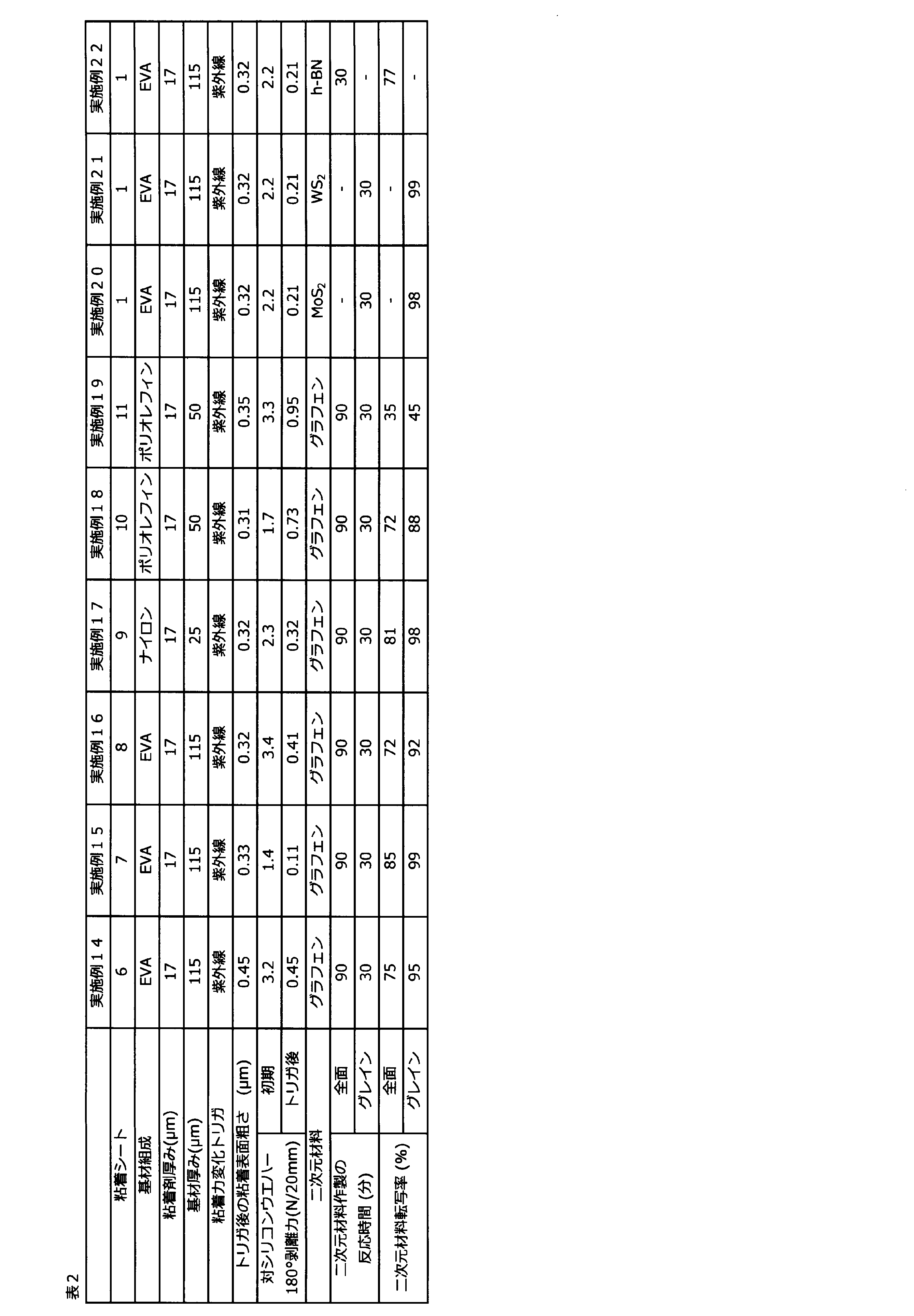
上記で作製した粘着シート1~3、6~11について、粘着シート1~3、6~11をそれぞれ幅20mm、長さ10cmになるように切断し、UV処理を行い、剥離ライナーを剥離除去した。
上記で作製した粘着シート4について、粘着シート4を幅20mm、長さ10cmになるように切断し、熱処理を行い、剥離ライナーを剥離除去した。
上記で作製した粘着シート5について、粘着シート5を幅20mm、長さ10cmになるように切断し、剥離ライナーを剥離除去した。
熱処理は150℃に加熱したホットプレート上に粘着シート4の基材側をホットプレートに接するようにして静置し1分後に取り出して空冷した。
上記で作製した粘着シート1~3、6~11について、UV処理前の粘着力(初期)を測定した。
粘着力の測定は、粘着シート1~3、6~11をそれぞれ幅20mm、長さ10cmになるように切断し、剥離ライナーを剥離除去した。
続いて、シリコンウエハー(4インチのシリコンミラーウエハー)に、各例の粘着シートを2kgローラーで1往復して圧着して貼付した。
引張試験機(AUTOGRAPH AGS-X、(株)島津製作所製)を用いて、剥離角度180度、剥離速度300mm/minで引きはがした際の力を粘着力(対シリコンウエハー180℃剥離力(初期))(N/20mm)として測定した。
UV処理は、UV照射機(日東精機社製 UM-810)で粘着シート1~3、6~11の基材側から450mJ/cm2の照射量で行った。
粘着力の測定は、粘着シート4を幅20mm、長さ10cmになるように切断し、剥離ライナーを剥離除去した。
続いて、シリコンウエハー(4インチのシリコンミラーウエハー)に、各例の粘着シートを2kgローラーで1往復して圧着して貼付した。
引張試験機(AUTOGRAPH AGS-X、(株)島津製作所製)を用いて、剥離角度180度、剥離速度300mm/minで引きはがした際の力を粘着力(初期)(N/20mm)として測定した。
熱処理は150℃に加熱したホットプレート上にシリコンウエハー側をホットプレートに接するようにして静置し1分後に取り出して空冷した。
粘着力の測定は、粘着シート5を幅20mm、長さ10cmになるように切断し、剥離ライナーを剥離除去した。
続いて、シリコンウエハー(4インチのシリコンミラーウエハー)に、各例の粘着シートを2kgローラーで1往復して圧着して貼付した。
引張試験機(AUTOGRAPH AGS-X、(株)島津製作所製)を用いて、剥離角度180度、剥離速度300mm/minで引きはがした際の力を粘着力(初期)(N/20mm)として測定した。
(グラフェンの転写率(全面))
実施例1~3、14~19、比較例1,2で得られたシリコン基板とグラフェンとの積層体(全面)の、被転写材の表面に残るグラフェンの像を、金属顕微鏡(Nikon製 ME600)とCCDカメラ(Nikon製 DS-Fi1)によるデジタル画像として取得した。なお、デジタル画像は、対物レンズ50倍の観察像で、その視野は160μm×120μmであり、任意の3箇所のデジタル画像を取得した。取得したデジタル画像を用いてソフトウェア「Win ROOF」(三谷商事製)にてRGB分離ならびに各成分像の二値化解析を行い、該当デジタル画像中に占めるグラフェンの面積比を百分率で求めた。3箇所のデジタル画像中に占めるグラフェンの面積比の平均値を転写率(全面)とした。
上記でCu/サファイア基板上にグラフェンを成膜した積層体1a(グレイン)を水中で酸化処理した後、粘着シート1を貼り付ける前に、Cu/サファイア基板上のグラフェン(グレイン)の観察像を、金属顕微鏡(Nikon製 ME600)とCCDカメラ(Nikon製 DS-Fi1)によるデジタル画像として取得した。
なお、デジタル画像は、対物レンズ50倍の観察像で、その視野は160μm×120μmであり、任意の3箇所のデジタル画像を取得した。
また、図7は、粘着テープにより転写された被転写材上の二次元材料結晶粒群として、実施例1のシリコン基板とグラフェンとの積層体の表面のグラフェンの像を、金属顕微鏡(Nikon製 ME600)とCCDカメラ(Nikon製 DS-Fi1)によるデジタル画像として取得したものである。
実施例2、3、14~19、及び比較例1~3についても同様に画像解析し、グレインの転写率を求めた。
積層体20aに粘着シート1を貼り付ける前に、CVDにより形成されたサファイア基板上のMoS2の観察像を、金属顕微鏡(Nikon製 ME600)とCCDカメラ(Nikon製 DS-Fi1)によるデジタル画像として取得した。なお、デジタル画像は、対物レンズ50倍の観察像で、その視野は160μm×120μmであり、任意の3箇所のデジタル画像を取得した。
つぎに、実施例20で得られたシリコン基板とMoS2との積層体の、被転写材(シリコン基板)の表面に残るMoS2の像を、先に取得したサファイア基板上のMoS2の観察像と対応する位置において、同様の金属顕微鏡とCCDカメラによるデジタル画像として取得した。先に取得したサファイア基板上のMoS2と対応する位置のシリコン基板のMoS2の面積比を百分率で求めた。3箇所のデジタル画像中に占めるMoS2の面積比の平均値を転写率とした。
同様の操作によりWS2の転写率(グレイン)を求めた。
グラフェンの転写率(全面)と同様の操作により、h-BNの転写率(全面)を求めた。


本出願は、2019年2月19日出願の日本特許出願(特願2019-027773)に基づくものであり、その内容はここに参照として取り込まれる。
10:粘着シート
11:基材
12:粘着剤層
21:第1の基板
30:二次元材料
40:第2の基板
105:二次元材料積層体
Claims (13)
- 第1の基板上の二次元材料を、基材と、紫外線または熱により粘着力が低下する粘着剤層とを有する粘着シートの該粘着剤層側の面に貼り合わせて転写し、該粘着シートと、該二次元材料との積層体を得る工程と、
前記積層体の前記二次元材料側の面が第2の基板に接するように、前記積層体を該第2の基板に載置する工程と、
前記積層体に前記紫外線または熱を与える工程と、
前記粘着シートを剥離することにより前記第2の基板上に前記二次元材料を転写する工程とを含み、
前記紫外線または熱を与える前の前記粘着剤層のシリコンウエハーに対する25℃における粘着力Aが、引張速度300mm/minで180°ピールを行ったとき、1.0N/20mm~20.0N/20mmであり、
前記紫外線または熱を与えた後の前記粘着剤層の粘着面の表面粗さが0.01μm~8.00μmである、
二次元材料積層体の製造方法。 - 前記二次元材料が、二次元炭素材料、二硫化モリブデン、二硫化タングステン、又は六方晶窒化ホウ素である、請求項1に記載の二次元材料積層体の製造方法。
- 前記紫外線または熱を与えた後の前記粘着剤層のシリコンウエハーに対する25℃における粘着力Bが、引張速度300mm/minで180°ピールを行ったとき、0.01N/20mm~1.00N/20mmである、請求項1又は2に記載の二次元材料積層体の製造方法。
- 前記二次元炭素材料が、グラフェン又はグラフェン誘導体である、請求項2に記載の二次元材料積層体の製造方法。
- 前記粘着剤層が、紫外線硬化型粘着剤を含む、請求項2~4のいずれか1項に記載の二次元材料積層体の製造方法。
- 前記基材が、紫外線透過性を有する、請求項2~5のいずれか1項に記載の二次元材料積層体の製造方法。
- 前記二次元材料の転写率が30%以上である請求項6に記載の二次元材料積層体の製造方法。
- 基材と、紫外線または熱により粘着力が低下する粘着剤層とを有する粘着シートと、二次元材料との積層体であって、
該紫外線または熱を与える前の粘着剤層のシリコンウエハーに対する25℃における粘着力Aが、引張速度300mm/minで180°ピールを行ったとき、1.0N/20mm~20.0N/20mmであり、
該紫外線または熱を与えた後の粘着剤層の粘着面の表面粗さが0.01μm~8.00μmである積層体。 - 前記二次元材料が、二次元炭素材料、二硫化モリブデン、二硫化タングステン、又は六方晶窒化ホウ素である、請求項8に記載の積層体。
- 前記紫外線または熱を与えた後の前記粘着剤層のシリコンウエハーに対する25℃における粘着力Bが、引張速度300mm/minで180°ピールを行ったとき、0.01N/20mm~1.00N/20mmである、請求項9に記載の積層体。
- 前記二次元炭素材料が、グラフェン又はグラフェン誘導体である、請求項9に記載の積層体。
- 前記粘着剤層が、紫外線硬化型粘着剤を含む、請求項9~11のいずれか1項に記載の積層体。
- 前記基材が、紫外線透過性を有する、請求項9~12のいずれか1項に記載の積層体。
Priority Applications (6)
| Application Number | Priority Date | Filing Date | Title |
|---|---|---|---|
| US17/432,345 US12263662B2 (en) | 2019-02-19 | 2020-02-14 | Method for producing laminate of two-dimensional material and laminate |
| ES20759093T ES3039924T3 (en) | 2019-02-19 | 2020-02-14 | Method for manufacturing laminate of two-dimensional material, and laminate |
| JP2021501945A JP7558517B2 (ja) | 2019-02-19 | 2020-02-14 | 二次元材料積層体の製造方法及び積層体 |
| CN202080015162.6A CN113453884A (zh) | 2019-02-19 | 2020-02-14 | 二维材料层叠体的制造方法及层叠体 |
| KR1020217026176A KR102815609B1 (ko) | 2019-02-19 | 2020-02-14 | 이차원 재료 적층체의 제조 방법 및 적층체 |
| EP20759093.6A EP3928977B1 (en) | 2019-02-19 | 2020-02-14 | Method for manufacturing laminate of two-dimensional material, and laminate |
Applications Claiming Priority (2)
| Application Number | Priority Date | Filing Date | Title |
|---|---|---|---|
| JP2019-027773 | 2019-02-19 | ||
| JP2019027773 | 2019-02-19 |
Publications (1)
| Publication Number | Publication Date |
|---|---|
| WO2020170977A1 true WO2020170977A1 (ja) | 2020-08-27 |
Family
ID=72143659
Family Applications (1)
| Application Number | Title | Priority Date | Filing Date |
|---|---|---|---|
| PCT/JP2020/005841 Ceased WO2020170977A1 (ja) | 2019-02-19 | 2020-02-14 | 二次元材料積層体の製造方法及び積層体 |
Country Status (8)
| Country | Link |
|---|---|
| US (1) | US12263662B2 (ja) |
| EP (1) | EP3928977B1 (ja) |
| JP (1) | JP7558517B2 (ja) |
| KR (1) | KR102815609B1 (ja) |
| CN (1) | CN113453884A (ja) |
| ES (1) | ES3039924T3 (ja) |
| TW (1) | TWI868110B (ja) |
| WO (1) | WO2020170977A1 (ja) |
Cited By (2)
| Publication number | Priority date | Publication date | Assignee | Title |
|---|---|---|---|---|
| US20220169002A1 (en) * | 2019-02-19 | 2022-06-02 | Nitto Denko Corporation | Method for producing laminate of two-dimensional material and laminate |
| WO2026004596A1 (ja) * | 2024-06-25 | 2026-01-02 | 太陽ホールディングス株式会社 | 第1積層構造体、第2積層構造体、及びプリント配線板の製造方法 |
Families Citing this family (13)
| Publication number | Priority date | Publication date | Assignee | Title |
|---|---|---|---|---|
| US12004308B2 (en) * | 2021-05-18 | 2024-06-04 | Mellanox Technologies, Ltd. | Process for laminating graphene-coated printed circuit boards |
| US12163228B2 (en) | 2021-05-18 | 2024-12-10 | Mellanox Technologies, Ltd. | CVD system with substrate carrier and associated mechanisms for moving substrate therethrough |
| US12221695B2 (en) | 2021-05-18 | 2025-02-11 | Mellanox Technologies, Ltd. | CVD system with flange assembly for facilitating uniform and laminar flow |
| US12289839B2 (en) | 2021-05-18 | 2025-04-29 | Mellanox Technologies, Ltd. | Process for localized repair of graphene-coated lamination stacks and printed circuit boards |
| US11963309B2 (en) | 2021-05-18 | 2024-04-16 | Mellanox Technologies, Ltd. | Process for laminating conductive-lubricant coated metals for printed circuit boards |
| CN113352729A (zh) * | 2021-06-21 | 2021-09-07 | 苏州鸿凌达电子科技有限公司 | 一种基于六方氮化硼复合导热膜的加工方法 |
| KR102668464B1 (ko) * | 2021-11-15 | 2024-05-24 | 한국에너지기술연구원 | 2차원 tmd 물질로 접촉 특성이 개선된 투명 전극, 이를 적용한 전자 소자 및 투명 전극의 형성방법 |
| CN114478022B (zh) * | 2021-12-31 | 2023-01-03 | 南通威斯派尔半导体技术有限公司 | 一种高可靠性氮化铝覆铜陶瓷基板及其制备方法 |
| WO2024091381A1 (en) * | 2022-10-28 | 2024-05-02 | Applied Materials, Inc. | Release layer for alkali metal on plastic substrates |
| US20240397636A1 (en) * | 2023-05-22 | 2024-11-28 | Nvidia Corporation | Method for integrating a copper-graphene laminate (cgl) in a multilayer pcb fabrication process |
| US20250037979A1 (en) * | 2023-07-28 | 2025-01-30 | Applied Materials, Inc. | Resilient release layer for lithium film transfer and atmospheric plasma assisted removal of residual release layer |
| US20260061734A1 (en) * | 2024-09-03 | 2026-03-05 | Elevated Materials Us Llc | Metal or alloy film release by low sublimation release layer for electrochemical device |
| CN120155357B (zh) * | 2025-05-12 | 2025-07-25 | 深圳市哈德胜精密科技股份有限公司 | 一种基于转印技术的图形胶水显色定位方法 |
Citations (6)
| Publication number | Priority date | Publication date | Assignee | Title |
|---|---|---|---|---|
| JPS5850720B2 (ja) | 1974-09-12 | 1983-11-11 | コマンデイ−トゲゼルシヤフト・シユヴアルツハウプト | テクテ−トデヒドロゲナ−ゼのイソチ−ム4及び5を一緒に測定する試薬 |
| JP2008115273A (ja) * | 2006-11-04 | 2008-05-22 | Nitto Denko Corp | 熱剥離性粘着シート及び被着体回収方法 |
| JP2014172989A (ja) | 2013-03-08 | 2014-09-22 | Nitto Denko Corp | 脆弱部材仮固定用粘着部材 |
| US20160240692A1 (en) * | 2013-08-09 | 2016-08-18 | The Trustees Of Columbia University In The City Of New York | Systems and methods for assembling two-dimensional materials |
| JP2019008089A (ja) * | 2017-06-23 | 2019-01-17 | 信越化学工業株式会社 | フォトリソグラフィ用ペリクル膜及びペリクル |
| JP2019027773A (ja) | 2017-07-31 | 2019-02-21 | ダイキン工業株式会社 | 空気調和システム |
Family Cites Families (9)
| Publication number | Priority date | Publication date | Assignee | Title |
|---|---|---|---|---|
| CN101031625A (zh) | 2004-10-01 | 2007-09-05 | 东洋油墨制造株式会社 | 活性能量射线粘合力消失型压敏粘合剂、涂布其的活性能量射线粘合力消失型粘合片和蚀刻化金属体的制造方法 |
| WO2009050785A1 (ja) | 2007-10-16 | 2009-04-23 | Denki Kagaku Kogyo Kabushiki Kaisha | 粘着剤、粘着シート、多層粘着シート及び電子部品の製造方法 |
| JP5727688B2 (ja) | 2008-03-31 | 2015-06-03 | リンテック株式会社 | エネルギー線硬化型重合体、エネルギー線硬化型粘着剤組成物、粘着シートおよび半導体ウエハの加工方法 |
| CN103596879B (zh) | 2011-06-02 | 2018-06-12 | Jx日矿日石金属株式会社 | 石墨烯制造用铜箔以及石墨烯的制造方法 |
| JP5850720B2 (ja) | 2011-06-02 | 2016-02-03 | Jx日鉱日石金属株式会社 | グラフェン製造用銅箔、及びグラフェンの製造方法 |
| WO2013186858A1 (ja) * | 2012-06-12 | 2013-12-19 | グラフェンプラットフォーム株式会社 | グラフェン積層体およびグラフェン積層体の製造方法 |
| JP2015076276A (ja) | 2013-10-09 | 2015-04-20 | 日東電工株式会社 | 電解質膜搬送用粘着シートおよび該粘着シートを用いた燃料電池用膜/電極複合体の製造方法 |
| JP2015097195A (ja) | 2013-10-09 | 2015-05-21 | 日東電工株式会社 | 燃料電池用膜/電極複合体の製造方法 |
| US12263662B2 (en) * | 2019-02-19 | 2025-04-01 | Nitto Denko Corporation | Method for producing laminate of two-dimensional material and laminate |
-
2020
- 2020-02-14 US US17/432,345 patent/US12263662B2/en active Active
- 2020-02-14 EP EP20759093.6A patent/EP3928977B1/en active Active
- 2020-02-14 JP JP2021501945A patent/JP7558517B2/ja active Active
- 2020-02-14 KR KR1020217026176A patent/KR102815609B1/ko active Active
- 2020-02-14 ES ES20759093T patent/ES3039924T3/es active Active
- 2020-02-14 CN CN202080015162.6A patent/CN113453884A/zh active Pending
- 2020-02-14 WO PCT/JP2020/005841 patent/WO2020170977A1/ja not_active Ceased
- 2020-02-18 TW TW109105124A patent/TWI868110B/zh active
Patent Citations (6)
| Publication number | Priority date | Publication date | Assignee | Title |
|---|---|---|---|---|
| JPS5850720B2 (ja) | 1974-09-12 | 1983-11-11 | コマンデイ−トゲゼルシヤフト・シユヴアルツハウプト | テクテ−トデヒドロゲナ−ゼのイソチ−ム4及び5を一緒に測定する試薬 |
| JP2008115273A (ja) * | 2006-11-04 | 2008-05-22 | Nitto Denko Corp | 熱剥離性粘着シート及び被着体回収方法 |
| JP2014172989A (ja) | 2013-03-08 | 2014-09-22 | Nitto Denko Corp | 脆弱部材仮固定用粘着部材 |
| US20160240692A1 (en) * | 2013-08-09 | 2016-08-18 | The Trustees Of Columbia University In The City Of New York | Systems and methods for assembling two-dimensional materials |
| JP2019008089A (ja) * | 2017-06-23 | 2019-01-17 | 信越化学工業株式会社 | フォトリソグラフィ用ペリクル膜及びペリクル |
| JP2019027773A (ja) | 2017-07-31 | 2019-02-21 | ダイキン工業株式会社 | 空気調和システム |
Non-Patent Citations (1)
| Title |
|---|
| See also references of EP3928977A4 |
Cited By (3)
| Publication number | Priority date | Publication date | Assignee | Title |
|---|---|---|---|---|
| US20220169002A1 (en) * | 2019-02-19 | 2022-06-02 | Nitto Denko Corporation | Method for producing laminate of two-dimensional material and laminate |
| US12263662B2 (en) * | 2019-02-19 | 2025-04-01 | Nitto Denko Corporation | Method for producing laminate of two-dimensional material and laminate |
| WO2026004596A1 (ja) * | 2024-06-25 | 2026-01-02 | 太陽ホールディングス株式会社 | 第1積層構造体、第2積層構造体、及びプリント配線板の製造方法 |
Also Published As
| Publication number | Publication date |
|---|---|
| KR20210128407A (ko) | 2021-10-26 |
| CN113453884A (zh) | 2021-09-28 |
| TWI868110B (zh) | 2025-01-01 |
| JP7558517B2 (ja) | 2024-10-01 |
| JPWO2020170977A1 (ja) | 2020-08-27 |
| EP3928977A1 (en) | 2021-12-29 |
| US12263662B2 (en) | 2025-04-01 |
| EP3928977A4 (en) | 2022-11-09 |
| ES3039924T3 (en) | 2025-10-27 |
| EP3928977C0 (en) | 2025-08-27 |
| KR102815609B1 (ko) | 2025-05-30 |
| TW202103968A (zh) | 2021-02-01 |
| EP3928977B1 (en) | 2025-08-27 |
| US20220169002A1 (en) | 2022-06-02 |
Similar Documents
| Publication | Publication Date | Title |
|---|---|---|
| US12263662B2 (en) | Method for producing laminate of two-dimensional material and laminate | |
| JP4800778B2 (ja) | ダイシング用粘着シート及びそれを用いた被加工物の加工方法 | |
| JP4970863B2 (ja) | 被加工物の加工方法 | |
| CN101942278A (zh) | 半导体晶圆切割用粘合片和半导体晶圆的切割方法 | |
| JP5313837B2 (ja) | 再剥離性粘着シート | |
| CN103081070A (zh) | 切割用粘合片及使用了切割用粘合片的半导体装置的制造方法 | |
| KR20070027464A (ko) | 점착 시트 및 이 점착 시트를 이용한 제품의 가공 방법 | |
| JP5631082B2 (ja) | 活性エネルギー線硬化型再剥離用粘着剤 | |
| TW202405113A (zh) | 電子零件暫時固定用黏著片材 | |
| JP5631081B2 (ja) | 活性エネルギー線硬化型再剥離用粘着剤 | |
| JP7850704B2 (ja) | 表面保護シート | |
| JP7850703B2 (ja) | 表面保護シートおよび処理方法 | |
| JP5495985B2 (ja) | 活性エネルギー線硬化型再剥離用粘着剤 | |
| WO2025143072A1 (ja) | 粘着シート及び接合体 | |
| JP7834845B2 (ja) | ピールテープ及び粘接着材を用いたウエハの製造方法、並びにその方法に用いるピールテープ及び粘接着材 | |
| JP7850702B2 (ja) | 表面保護シートおよび処理方法 | |
| WO2025143071A1 (ja) | 積層体の製造方法、二次元材料積層体の製造方法及び二次元材料を含む積層体の製造装置 | |
| WO2025143070A1 (ja) | 積層体の製造方法、二次元材料積層体の製造方法及び二次元材料 | |
| TWI921467B (zh) | 表面保護片材及處理方法 | |
| JP7764180B2 (ja) | 電子部品仮固定用粘着シートおよび電子部品の処理方法 | |
| JP5495987B2 (ja) | 活性エネルギー線硬化型再剥離用粘着剤 | |
| TWI889721B (zh) | 半導體加工用積層體、半導體加工用黏著帶、及半導體裝置之製造方法 | |
| TW202613274A (zh) | 積層體之製造方法、二次元材料積層體之製造方法及含有二次元材料之積層體之製造裝置 | |
| WO2023145360A1 (ja) | 表面保護シートおよび処理方法 |
Legal Events
| Date | Code | Title | Description |
|---|---|---|---|
| 121 | Ep: the epo has been informed by wipo that ep was designated in this application |
Ref document number: 20759093 Country of ref document: EP Kind code of ref document: A1 |
|
| ENP | Entry into the national phase |
Ref document number: 2021501945 Country of ref document: JP Kind code of ref document: A |
|
| NENP | Non-entry into the national phase |
Ref country code: DE |
|
| ENP | Entry into the national phase |
Ref document number: 2020759093 Country of ref document: EP Effective date: 20210920 |
|
| WWG | Wipo information: grant in national office |
Ref document number: 17432345 Country of ref document: US |
|
| WWG | Wipo information: grant in national office |
Ref document number: 2020759093 Country of ref document: EP |