WO2020174558A1 - 基板、電子部品及び実装装置 - Google Patents
基板、電子部品及び実装装置 Download PDFInfo
- Publication number
- WO2020174558A1 WO2020174558A1 PCT/JP2019/007192 JP2019007192W WO2020174558A1 WO 2020174558 A1 WO2020174558 A1 WO 2020174558A1 JP 2019007192 W JP2019007192 W JP 2019007192W WO 2020174558 A1 WO2020174558 A1 WO 2020174558A1
- Authority
- WO
- WIPO (PCT)
- Prior art keywords
- layer
- redox
- metal layer
- insulating layer
- metal
- Prior art date
- Legal status (The legal status is an assumption and is not a legal conclusion. Google has not performed a legal analysis and makes no representation as to the accuracy of the status listed.)
- Ceased
Links
Images


Classifications
-
- B—PERFORMING OPERATIONS; TRANSPORTING
- B32—LAYERED PRODUCTS
- B32B—LAYERED PRODUCTS, i.e. PRODUCTS BUILT-UP OF STRATA OF FLAT OR NON-FLAT, e.g. CELLULAR OR HONEYCOMB, FORM
- B32B15/00—Layered products comprising a layer of metal
- B32B15/04—Layered products comprising a layer of metal comprising metal as the main or only constituent of a layer, which is next to another layer of the same or of a different material
-
- B—PERFORMING OPERATIONS; TRANSPORTING
- B32—LAYERED PRODUCTS
- B32B—LAYERED PRODUCTS, i.e. PRODUCTS BUILT-UP OF STRATA OF FLAT OR NON-FLAT, e.g. CELLULAR OR HONEYCOMB, FORM
- B32B3/00—Layered products comprising a layer with external or internal discontinuities or unevennesses, or a layer of non-planar shape; Layered products comprising a layer having particular features of form
- B32B3/26—Layered products comprising a layer with external or internal discontinuities or unevennesses, or a layer of non-planar shape; Layered products comprising a layer having particular features of form characterised by a particular shape of the outline of the cross-section of a continuous layer; characterised by a layer with cavities or internal voids ; characterised by an apertured layer
- B32B3/30—Layered products comprising a layer with external or internal discontinuities or unevennesses, or a layer of non-planar shape; Layered products comprising a layer having particular features of form characterised by a particular shape of the outline of the cross-section of a continuous layer; characterised by a layer with cavities or internal voids ; characterised by an apertured layer characterised by a layer formed with recesses or projections, e.g. hollows, grooves, protuberances, ribs
-
- H—ELECTRICITY
- H05—ELECTRIC TECHNIQUES NOT OTHERWISE PROVIDED FOR
- H05K—PRINTED CIRCUITS; CASINGS OR CONSTRUCTIONAL DETAILS OF ELECTRIC APPARATUS; MANUFACTURE OF ASSEMBLAGES OF ELECTRICAL COMPONENTS
- H05K3/00—Apparatus or processes for manufacturing printed circuits
- H05K3/02—Apparatus or processes for manufacturing printed circuits in which the conductive material is applied to the surface of the insulating support and is thereafter removed from such areas of the surface which are not intended for current conducting or shielding
- H05K3/06—Apparatus or processes for manufacturing printed circuits in which the conductive material is applied to the surface of the insulating support and is thereafter removed from such areas of the surface which are not intended for current conducting or shielding the conductive material being removed chemically or electrolytically, e.g. by photo-etch process
-
- H—ELECTRICITY
- H05—ELECTRIC TECHNIQUES NOT OTHERWISE PROVIDED FOR
- H05K—PRINTED CIRCUITS; CASINGS OR CONSTRUCTIONAL DETAILS OF ELECTRIC APPARATUS; MANUFACTURE OF ASSEMBLAGES OF ELECTRICAL COMPONENTS
- H05K3/00—Apparatus or processes for manufacturing printed circuits
- H05K3/10—Apparatus or processes for manufacturing printed circuits in which conductive material is applied to the insulating support in such a manner as to form the desired conductive pattern
- H05K3/20—Apparatus or processes for manufacturing printed circuits in which conductive material is applied to the insulating support in such a manner as to form the desired conductive pattern by affixing prefabricated conductor pattern
-
- H—ELECTRICITY
- H05—ELECTRIC TECHNIQUES NOT OTHERWISE PROVIDED FOR
- H05K—PRINTED CIRCUITS; CASINGS OR CONSTRUCTIONAL DETAILS OF ELECTRIC APPARATUS; MANUFACTURE OF ASSEMBLAGES OF ELECTRICAL COMPONENTS
- H05K3/00—Apparatus or processes for manufacturing printed circuits
- H05K3/38—Improvement of the adhesion between the insulating substrate and the metal
Definitions
- the present invention relates to a substrate having an insulating layer and a metal layer, an electronic component and a mounting device using the substrate.
- a substrate such as CCL has an insulating layer such as a polyimide film. Then, in order to improve the adhesion between the metal layer and the insulating layer, it has been proposed to provide an adhesion layer containing polyimide and a particulate metal between the metal layer and the insulating layer (see, for example, Patent Document 1). ..).
- Patent Document 1 Providing a separate adhesion layer containing a particulate metal as shown in Patent Document 1 is different from the designed current flow because at least a part of the current flows through the particulate metal in the adhesion layer. A current flow will occur.
- the present invention provides a substrate, an electronic component, and a mounting device that can improve the adhesion between the metal layer and the insulating layer while preventing the occurrence of a current flow different from the current flow due to the design.
- the substrate according to the invention comprises An insulating layer, A metal layer provided on the insulating layer, A redox layer provided between the insulating layer and the metal layer and having an uneven shape on the surface on the insulating layer side, May be provided.
- the redox layer may include an oxide of a material forming the metal layer.
- the redox layer may include a first redox layer and a second redox layer provided closer to the insulating layer than the first redox layer.
- the metal layer is copper
- the redox layer may include copper oxide as a main component.
- the redox layer may be made of copper oxide.
- the metal layer is patterned to have a substantially rectangular or substantially square cross section,
- the redox layer having an uneven shape may be provided on the insulating layer side of the metal layer.
- the metal layer is patterned to have a substantially rectangular cross section, An uneven shape may be formed only on the insulating layer side of the metal layer.
- the entire redox layer may be embedded in the insulating layer.
- a redox layer is provided on the other surface of the patterned metal layer and at least a part of the side surface of the metal layer, The redox layer may be embedded in the insulating layer.
- a redox layer may be provided on the other surface, side surface and one surface of the patterned metal layer.
- Part of the metal layer is embedded in the insulating layer,
- the redox layer is provided on the side surface of the metal layer embedded in the insulating layer,
- the redox layer may not be provided on the side surface of the metal layer exposed from the insulating layer.
- the insulating layer may include a first insulating layer and a resist layer provided on the first insulating layer.
- the electronic component according to the present invention is The above-mentioned substrate, An electronic component provided on the substrate, Equipped with The electronic component may be provided on the metal layer.
- the mounting apparatus according to the present invention is You may provide the electronic component mentioned above.
- the redox layer provided between the insulating layer and the metal layer and having the uneven surface is provided on the insulating layer side surface (the other surface)
- the redox having the uneven shape is adopted.
- the layer can increase the peel strength (adhesion) between the metal layer and the insulating layer.
- the redox layer is provided with an uneven shape for enhancing the adhesion with the insulating layer and such an uneven shape is not provided in the metal layer, it is possible to prevent the current flowing through the metal layer from being disturbed. ..
- FIG. 3 is a cross-sectional view showing one mode in which the entire redox layer and a part of the metal layer are embedded in the insulating layer in the substrate according to the embodiment of the present invention.
- FIG. 7 is a cross-sectional view showing another mode in which the entire redox layer and a part of the metal layer are embedded in the insulating layer in the substrate according to the embodiment of the present invention.
- Sectional drawing which showed an example of the manufacturing process of the board
- Sectional drawing which continued from FIG. 7 and which showed an example of the manufacturing process of the board
- FIG. 6 is a cross-sectional view showing a mode in which a material layer is provided in the substrate according to the embodiment of the present invention. Sectional drawing which showed the 1st aspect which an insulating layer has a 1st insulating layer and a resist layer in the board
- substrate by embodiment of this invention Sectional drawing which showed the 3rd aspect which an insulating layer has a 1st insulating layer and a resist layer in the board
- Sectional drawing which showed the 6th aspect which an insulating layer has a 1st insulating layer and a resist layer in the board
- Sectional drawing which showed the 7th aspect which the insulating layer has a 1st insulating layer and a resist layer in the board
- the substrate according to the present embodiment is, for example, CCL (Copper Clad Laminate).
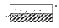
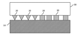
- the substrate may have an insulating layer 10 and a metal layer 30 provided on the insulating layer 10. Between the insulating layer 10 and the metal layer 30, a redox layer 20 having an uneven shape on the surface on the insulating layer 10 side may be provided.
- the substrate provided in this embodiment may be a printed circuit board, a metal-clad laminate such as a copper-clad laminate, or the like.
- the insulating layer 10 may be made of, for example, resin, glass, ceramic or the like.
- the insulating layer 10 may be a mixture of two or more insulating substances.
- the insulating layer 10 may include a fibrous or granular insulator.
- the insulating layer 10 may be a semi-cured sheet (prepreg) obtained by impregnating a base material such as paper or glass fiber with a resin and drying the base material.
- the insulating layer 10 may contain a heat conductive material such as silicon nitride.
- thermoplastic resin may be used as the material of the insulating layer 10 as long as it has a certain heat resistance.
- thermosetting resin polyimide resin, epoxy resin, phenol resin, cyanate resin or the like may be used.
- the thermoplastic resin may have a heat distortion temperature of 50 degrees or higher.
- the metal layer 30 may be metal foil, metal plating, rolled plate, or the like.
- the redox layer 20 may include an oxide of the material forming the metal layer 30. Further, the redox layer 20 may be wholly or partially formed in an uneven shape.
- the uneven shape may have a substantially triangular cross section (see FIG. 2 ), a substantially rectangular shape (see FIG. 2 ), or a substantially semicircular shape (see FIG. 3 ). ), a substantially circular shape (see FIG. 3 ), a mesh shape in which fibers are entangled with each other, and an uneven shape may be formed in various shapes.
- substantially XX shape means that the shape is approximately XX when seen by those skilled in the art.
- the metal layer 30 may be copper.
- the redox layer 20 may include copper oxide as a main component.
- the copper oxide may include cuprous oxide, cupric oxide, or both cuprous oxide and cupric oxide.
- the term "main component" means that the main component is contained in an amount exceeding 50% by weight.
- the metal layer 30 may be other than copper, and may be, for example, gold, silver, aluminum, nickel, or an alloy containing these metals.
- the thickness of the metal layer 30 may be 10 ⁇ m to 60 ⁇ m, or 18 ⁇ m to 45 ⁇ m.
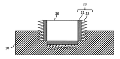
- the redox layer 20 may include a first redox layer 21 and a second redox layer 22 provided on the insulating layer side of the first redox layer 21.
- the first redox layer 21 contains cuprous oxide (Cu 2 O)
- the second redox layer 22 contains cupric oxide (CuO). May be included.
- the first redox layer 21 may be made of cuprous oxide (Cu 2 O)
- the second redox layer 22 may be made of cupric oxide (CuO).
- the redox layer 20 may be composed only of copper oxide. That is. All of the redox layer 20 may be made of copper oxide.
- the copper oxide may be cuprous oxide (Cu 2 O), cupric oxide (CuO), or both cuprous oxide and cupric oxide. Since the cuprous oxide becomes cupric oxide as the oxidation reaction proceeds, the treatment time by the treatment liquid 120 (see FIG. 7A) is adjusted to mix the cuprous oxide and the cupric oxide. The ratio may be adjusted.
- the minimum value is 1.090 N/mm, It was confirmed that the peel strength had a maximum value of 1.150 N/mm and an average value of 1.115 N/mm.
- the minimum value is 1.606 N/mm. It was confirmed that the peel strength had a maximum value of 1.784 N/mm and an average value of 1.691 N/mm.
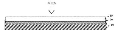
- the surface of the metal layer 30 positioned on the insulating layer 10 side (hereinafter, also referred to as “the other surface” and may be referred to as the “rear surface”) is treated with the treatment liquid 120, so that the oxidation reduction is performed.
- Layer 20 may be formed.
- the redox layer 20 may be formed by immersing the other surface of the metal layer 30 in the treatment liquid 120 for a predetermined time, or after the treatment liquid 120 is applied to the other surface of the metal layer 30 and a predetermined time has elapsed.
- the redox layer 20 may be formed by removing the treatment liquid 120.
- an alkaline processing liquid 120 such as NaClO 2 or NaOH may be used.
- the oxidation-reduction layer 20 having an uneven shape may be formed by treating the other surface of the metal layer 30 with the treatment liquid 120. More specifically, the other surface of the metal layer 30 is treated with the treatment liquid 120 to cause a chemical reaction such as a redox reaction, and as a result, the redox layer 20 having an uneven shape may be formed. ..
- the treatment with the treatment liquid 120 is performed only on the other surface side of the metal layer 30, and may not be performed on the one surface side.
- the cross-sectional area of the metal layer 30 through which the current effectively flows is formed by forming the oxidation-reduction layer 20 having an uneven shape only on the other surface side for ensuring the peel strength and not providing the uneven shape at other portions.
- the present invention is not limited to such an aspect, and the redox layer 20 may be formed on the side surface and/or one surface side of the metal layer 30 (see FIGS. 12 and 13).
- the redox layer 20 may be formed on the side surface and/or one surface side of the metal layer 30 (see FIGS. 12 and 13).
- the peel strength with respect to the substrate located on the one surface can be increased.
- peel strength can be increased by providing the redox layer 20 having an uneven shape on the side surface of the metal layer 30. it can.
- the redox layer 20 should not be provided in the portion not embedded in the insulating layer 10 as shown in the upper side of FIG. Alternatively, as shown in FIG. 12, a portion of the redox layer 20 which is not buried in the insulating layer 10 may be left.
- the other surface of the metal layer 30 is treated with the treatment liquid 120 for a relatively long time of 15 to 20 minutes in order to form the redox layer 20 having an uneven shape with a sufficient size to secure the peel strength. You may. Further, it can be confirmed that the metal layer 30 having a substantially flat shape can be formed on the other surface side by performing the treatment with the treatment liquid 120 for a sufficient time in this manner, and thus the current flow can be stabilized. ing.
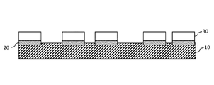
- the metal layer 30 may be patterned for various designs such as circuit design (see FIG. 7D).
- the patterned metal layer 30 may have a substantially rectangular cross section.
- the “rectangular shape” is a shape including various rectangles such as a square, a rectangle, and a trapezoid.
- the "substantially rectangular shape” of the present embodiment includes a mode having unevenness that is unavoidably formed on the surface.
- the metal layer 30 may have a substantially rectangular shape or a substantially square shape.
- a substantially rectangular shape means that one side (upper side) has a length of 70% or more of the other side (lower side) in the cross section. ..
- the difference between the length in the thickness direction and the length of the side on one side in the cross section is within ⁇ 5% of the longer of the length in the thickness direction and the length of the side on one side. It means that there is.
- the length of one side of the patterned metal layer 30 is preferably 80% or more, more preferably 90% or more, and more preferably 95% or more of the length of the other side. Are even more preferred.
- one side of the metal layer 30 is formed. A mode in which the side length is 90% or more and a mode in which the side length is 95% or more of the length of the other side can be realized.
- the cross section is formed into a trapezoidal shape, and thus the length of one side of the metal layer 30 is equal to that of the other side.
- At least a portion of the uneven redox layer 20 may be embedded in the insulating layer 10 (see FIG. 9), or the entire redox layer 20 may be embedded in the insulating layer 10 (see FIG. 2 and (See FIG. 3). Further, the redox layer 20 may be placed on one surface (the upper surface of FIG. 10) of the insulating layer 10 and the redox layer 20 may not be embedded in the insulating layer 10 (see FIG. 10). However, from the viewpoint of increasing the peel strength, it is preferable that at least a part of the redox layer 20 is embedded in the insulating layer 10 (see FIG. 9), and the entire redox layer 20 is embedded in the insulating layer 10. Is more preferable (see FIGS. 2 and 3).
- “embedded” means being located on the other side (lower side of the cross section of FIG. 2 etc.) than the one side (may be referred to as “front side”). That is, “embedded in the insulating layer 10 ”means that it is located on the other side (lower side) than one surface of the insulating layer 10.
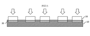
- the insulating layer 10 may be in a semi-cured state. Part or all of the patterned metal layer 30 may be embedded in the semi-cured insulating layer 10 by pressing (see FIGS. 5 and 6). When a part of the metal layer 30 is embedded in the insulating layer 10, for example, the entire redox layer 20 and a part of the side surface of the metal layer 30 may be embedded in the insulating layer 10. When the metal layer 30 is embedded in the insulating layer 10, a pressing force may be applied to the metal layer 30, but the present invention is not limited to this mode, and the metal layer 30 is embedded in the insulating layer 10 by its own weight.
- the patterned metal layer 30 and the redox layer 20 may be embedded in the insulating layer 10 (see FIG. 5), or before patterning.
- the metal layer 30 and the redox layer 20 may be embedded in the insulating layer 10 (see FIG. 6).
- the insulating layer 10 may be hardened by applying heat or irradiating ultraviolet rays.
- the insulating layer 10 may be cured by allowing it to cool or cool.
- a material layer 200 that is slower in etching than the metal layer 30 may be provided on one surface of the metal layer 30.
- This material layer 200 is a layer different from the resist layer.
- the material layer 200 may be made of a metal different from the metal layer 30, and when the metal layer 30 is made of a first metal, the material layer 200 may be made of a second metal.
- a nickel layer may be used as the slow-etching material layer 200. This material layer 200 may eventually be removed.
- the etching liquid is first used to dissolve the material layer 200, a more rectangular metal layer 30 can be obtained.
- the redox layer 20 provided between the insulating layer 10 and the metal layer 30 and having the uneven surface forms a metal.
- the peel strength (adhesion) between the layer 30 and the insulating layer 10 can be increased.
- the redox layer 20 is provided with an uneven shape for enhancing the adhesion with the insulating layer 10 and such an uneven shape is not provided in the metal layer 30, the current flowing through the metal layer 30 is disturbed. Can be prevented. That is, when an uneven shape is formed on the surface of the metal layer 30 as shown in FIG. 14, it is necessary to design a circuit in consideration of the current flowing in the uneven shape.
- the current flowing in such a concavo-convex shape may flow in a mode different from the design.
- the uneven shape of the surface of the metal layer 30 causes the current to flow. Can be prevented from being disturbed, and the adverse effect on the millimeter wave can be prevented. Therefore, the current can flow more accurately according to the design. Since no current flows in the redox layer 20, even if the redox layer 20 has an uneven shape, there is no problem from the viewpoint of current disturbance. Further, as described above, the patterned metal layer 30 having a substantially rectangular shape or a substantially square shape can realize a current closer to the design value.
- the metal layer 20 contains an oxide of the material forming the metal layer 30 and the redox layer 20 is formed by oxidizing a part of the metal layer 30, the metal layer is used without using another material. This is advantageous in that the redox layer 20 can be formed only by oxidizing 30.
- the redox layer 20 contains copper oxide as a main component
- a portion oxidized by oxidizing the metal layer 30 made of copper is used as the redox layer 20. It is beneficial in that it can be done.
- the first treatment liquid is used to form the first redox layer 21.
- a second treatment liquid different from the first treatment liquid may be used to form the second reduction layer 22.
- the first redox layer 21 may be formed by treating the metal layer 30 with the first treatment liquid.
- the second redox layer 22 may be formed by treating a part or all of the first redox layer 21 with the second treatment liquid.
- the first oxidation-reduction layer 21 and the second oxidation-reduction layer 22 may be formed by the same treatment liquid without being limited to such an aspect. More specifically, by treating the metal layer 30 with a predetermined treatment liquid, the first redox layer 21 is formed on the metal layer side and the second redox layer 22 is formed on the side away from the metal layer 30. You may do it. In the case of treating with the first treatment liquid, the second treatment liquid, or the predetermined treatment liquid as described above, the concentration of the treatment liquid, the temperature of the treatment liquid, the treatment time, and the like are adjusted to form the first redox layer 21. The thickness and the thickness of the second oxide reduction layer 22 may be controlled.
- a metal layer 30 made of copper foil or the like is prepared.
- the other surface of the metal layer 30 is dipped in the processing liquid 120 made of alkaline or the like stored in the container 110 for a predetermined time (see FIG. 7A).
- the redox layer 20 including the uneven shape is formed on the other surface of the metal layer 30 (see FIG. 7B).
- the other surface of the metal layer 30 may be cleaned to remove impurities and dirt.
- the first treatment liquid is used to form the first redox layer 21, and thereafter, A second treatment liquid different from the first treatment liquid may be used to form the second reduction layer 22.
- the present invention is not limited to such an aspect, and by treating the metal layer 30 with a predetermined treatment liquid, the first redox layer 21 is formed on the metal layer side and the first redox layer 21 is formed on the side away from the metal layer 30.
- the redox layer 22 may be formed.
- the other surface of the metal layer 30 is placed on one surface of the insulating layer 10 (see FIG. 7C).
- a resist is provided on one surface of the metal layer 30 and edging is performed.
- the metal layer 30 can be patterned and a circuit can be formed. Since the other surface of the metal layer 30 is treated with the treatment liquid 120 and placed on the insulating layer 10 as described above, patterning is performed, so that the one surface and the side surface of the patterned metal layer 30 are oxidized and reduced.
- the layer 20 is not formed, and the redox layer 20 can be formed only on the other surface side.
- Electronic components 60 such as semiconductor elements, capacitors, and resistors are placed on one surface of the metal layer 30 of the substrate formed as described above (see FIG. 8A).
- one side of the metal layer 30 is sealed with a sealing resin or the like, and an electronic component in which the electronic element is sealed by the sealing portion 90 is manufactured (see FIG. 8B).
- Such electronic components may be incorporated into any mounting device such as an automobile, an airplane, a ship, a helicopter, a personal computer, a home electric appliance, and the like.
- the mounting device is also provided. It is not always necessary to seal with a sealing resin or the like, and a mode in which a sealing portion such as a sealing resin is not provided can also be adopted.
- the metal layer 30 is pressed by a pressing member or the like so that the inside of the semi-cured insulating layer 10 is Alternatively, part of the redox layer 20, or the entire redox layer 20 and part of the metal layer 30 may be embedded (see FIG. 5).
- the present invention is not limited to such an aspect, and the metal layer 30 is pressed by a pressing member or the like before patterning, and a part of the redox layer 20 or the redox layer 20 in the insulating layer 10 in a semi-cured state. And the metal layer 30 may be partially embedded (see FIG. 6).
- the semi-cured insulating layer 10 may be cured by cooling or cooling.
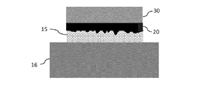
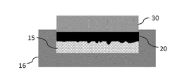
- the insulating layer 10 may have a resist layer 15 as shown in FIG.
- the first insulating layer 16 made of a resin or the like different from the resist layer 15 may be provided below the resist layer 15.
- the resist layer 15 may have the same insulating property as the first insulating layer 16 and may have a strong adhesive force with the first insulating layer 16.
- a resist layer 15, a redox layer 20 and a metal layer 30 may be provided on a part of the first insulating layer 16, and FIG. As shown, the metal layer 30 may be provided on a part of the redox layer 20.
- the layer may be selectively removed as appropriate to obtain a mode as shown in FIGS.
- the resist layer 15, the redox layer 20, and the metal layer 30 may be provided by being pressed into the first insulating layer 16.
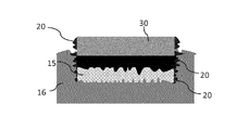
- the redox layer 20 having an uneven shape may be provided on the side surface of the metal layer 30 as shown in FIG. 20, or the metal layer 30 as shown in FIG.
- the redox layer 20 having an uneven shape may be provided on the side surface of the resist layer 15.
- the side surface of the redox layer 20 may also have an uneven shape.
- the surface of the first insulating layer 16 may be roughened as shown in FIG.
- Insulating layer 10 Insulating layer 20 Redox layer 30 Metal layer 60 Electronic component
Landscapes
- Engineering & Computer Science (AREA)
- Manufacturing & Machinery (AREA)
- Microelectronics & Electronic Packaging (AREA)
- Manufacturing Of Printed Wiring (AREA)
- Laminated Bodies (AREA)
Abstract
基板は、絶縁層10と、前記絶縁層10に設けられた金属層30と、前記絶縁層10と前記金属層30との間に設けられ、前記絶縁層10側の面で凹凸形状を有する酸化還元層20と、を有する。
Description
本発明は、絶縁層と金属層を有する基板と、当該基板を利用した電子部品及び実装装置に関する。
従来からCCL(Copper Clad Laminate)のような基板が知られている。CCLのような基板は、ポリイミドフィルム等の絶縁層と、を有している。そして、金属層と絶縁層との密着性を高めるために金属層と絶縁層との間にポリイミドと粒子状の金属を含有する密着層を設けることが提案されている(例えば、特許文献1参照。)。
特許文献1に示されるような粒子状の金属を含有する密着層を別途設けることは、密着層内の粒子状の金属に少なくとも一部の電流が流れることから、設計による電流の流れとは異なる電流の流れが発生してしまう。
本発明は、設計による電流の流れとは異なる電流の流れが発生することを防止しつつ、金属層と絶縁層との密着性を高めることができる基板、電子部品及び実装装置を提供する。
本発明による基板は、
絶縁層と、
前記絶縁層に設けられた金属層と、
前記絶縁層と前記金属層との間に設けられ、前記絶縁層側の面で凹凸形状を有する酸化還元層と、
を備えてもよい。
絶縁層と、
前記絶縁層に設けられた金属層と、
前記絶縁層と前記金属層との間に設けられ、前記絶縁層側の面で凹凸形状を有する酸化還元層と、
を備えてもよい。
本発明による基板において、
前記酸化還元層は前記金属層を構成する材料の酸化物を含んでもよい。
前記酸化還元層は前記金属層を構成する材料の酸化物を含んでもよい。
本発明による基板において、
前記酸化還元層は、第一酸化還元層と、前記第一酸化還元層よりも絶縁層側に設けられた第二酸化還元層とを有してもよい。
前記酸化還元層は、第一酸化還元層と、前記第一酸化還元層よりも絶縁層側に設けられた第二酸化還元層とを有してもよい。
本発明による基板において、
前記金属層は銅であり、
前記酸化還元層は主成分として酸化銅を含んでもよい。
前記金属層は銅であり、
前記酸化還元層は主成分として酸化銅を含んでもよい。
本発明による基板において、
前記酸化還元層は酸化銅からなってもよい。
前記酸化還元層は酸化銅からなってもよい。
本発明による基板において、
前記金属層はパターニングされ、横断面が略長方形状又は略正方形状となり、
前記金属層の前記絶縁層側に凹凸形状からなる前記酸化還元層が設けられてもよい。
前記金属層はパターニングされ、横断面が略長方形状又は略正方形状となり、
前記金属層の前記絶縁層側に凹凸形状からなる前記酸化還元層が設けられてもよい。
本発明による基板において、
前記金属層はパターニングされ、横断面が略矩形状となり、
前記金属層の前記絶縁層側だけに凹凸形状からなってもよい。
前記金属層はパターニングされ、横断面が略矩形状となり、
前記金属層の前記絶縁層側だけに凹凸形状からなってもよい。
本発明による基板において、
前記酸化還元層の全部が前記絶縁層に埋設されていてもよい。
前記酸化還元層の全部が前記絶縁層に埋設されていてもよい。
本発明による基板において、
パターニングされた金属層の他方面と、前記金属層の側面の少なくとも一部に酸化還元層が設けられ、
前記酸化還元層が前記絶縁層に埋設されていてもよい。
パターニングされた金属層の他方面と、前記金属層の側面の少なくとも一部に酸化還元層が設けられ、
前記酸化還元層が前記絶縁層に埋設されていてもよい。
本発明による基板において、
パターニングされた金属層の他方面、側面及び一方面に酸化還元層が設けられてもよい。
パターニングされた金属層の他方面、側面及び一方面に酸化還元層が設けられてもよい。
本発明による基板において、
前記金属層の一部が前記絶縁層内に埋設され、
前記絶縁層内に埋設される前記金属層の側面に前記酸化還元層が設けられ、
前記絶縁層から露出する前記金属層の側面には前記酸化還元層が設けられなくてもよい。
前記金属層の一部が前記絶縁層内に埋設され、
前記絶縁層内に埋設される前記金属層の側面に前記酸化還元層が設けられ、
前記絶縁層から露出する前記金属層の側面には前記酸化還元層が設けられなくてもよい。
本発明による基板において、
前記絶縁層は、第一絶縁層と、前記第一絶縁層に設けられたレジスト層とを有してもよい。
前記絶縁層は、第一絶縁層と、前記第一絶縁層に設けられたレジスト層とを有してもよい。
本発明による電子部品は、
前述した基板と、
前記基板に設けられた電子部品と、
を備え、
前記電子部品は前記金属層に設けられていてもよい。
前述した基板と、
前記基板に設けられた電子部品と、
を備え、
前記電子部品は前記金属層に設けられていてもよい。
本発明による実装装置は、
前述した電子部品を備えてもよい。
前述した電子部品を備えてもよい。
本発明において、絶縁層と金属層との間に設けられ、絶縁層側の面(他方面)で凹凸形状を有する酸化還元層が設けられる態様を採用した場合には、凹凸形状を有する酸化還元層によって金属層と絶縁層との間のピール強度(密着力)を高めることができる。また、絶縁層との密着性を高めるための凹凸形状が酸化還元層に設けられ、金属層にこのような凹凸形状が設けられないことから、金属層で流れる電流に乱れが生じることを防止できる。
実施の形態
《構成》
本実施の形態による基板は、例えばCCL(Copper Clad Laminate)である。基板は、図1に示すように、絶縁層10と、絶縁層10に設けられた金属層30と、を有してもよい。絶縁層10と金属層30との間に、絶縁層10側の面で凹凸形状を有する酸化還元層20が設けられてもよい。本実施の形態で提供される基板は、プリント基板、銅張積層板のような金属張積層板等であってもよい。
《構成》
本実施の形態による基板は、例えばCCL(Copper Clad Laminate)である。基板は、図1に示すように、絶縁層10と、絶縁層10に設けられた金属層30と、を有してもよい。絶縁層10と金属層30との間に、絶縁層10側の面で凹凸形状を有する酸化還元層20が設けられてもよい。本実施の形態で提供される基板は、プリント基板、銅張積層板のような金属張積層板等であってもよい。
絶縁層10は、例えば樹脂、ガラス、セラミック等から構成されてもよい。絶縁層10は、2種類以上の絶縁性の物質が混合されていてもよい。例えば、絶縁層10に、繊維状又は粒状の絶縁体が含まれていてもよい。絶縁層10は、紙やガラス繊維等の基材に樹脂を含浸させ、乾燥処理した半硬化状態のシート(プリプレグ)であってもよい。絶縁層10は、窒化ケイ素等の熱伝導物質を含有してもよい。
絶縁層10の材料としては、熱効硬化型樹脂、紫外線硬化型樹脂等を用いてもよい。一定の耐熱性があれば、絶縁層10の材料として熱可塑性樹脂を用いてもよい。熱硬化性の樹脂としては、ポリイミド樹脂、エポキシ樹脂、フェノール樹脂、シアネート樹脂等を用いてもよい。熱可塑性樹脂は、熱変形温度が50度以上であってもよい。
金属層30は、金属箔、金属めっき、圧延板等であってもよい。
酸化還元層20は金属層30を構成する材料の酸化物を含んでもよい。また、酸化還元層20はその全部又は一部が凹凸形状からなってもよい。凹凸形状は、断面が略三角形状であってもよいし(図2参照)、略矩形状であってもよいし(図2参照)、略半円形状であってもよいし(図3参照)、略円形状であってもよく(図3参照)、繊維が絡み合ったような網目形状となってもよく、凹凸形状は様々な形状として構成されてもよい。本実施の形態において「略○○形状」とは、当業者が見たときに概ね〇〇形状であることを意味している。
金属層30は銅であってもよい。酸化還元層20は主成分として酸化銅を含んでもよい。酸化銅は、酸化第1銅、酸化第2銅、又は酸化第1銅及び酸化第2銅の両方を含んでもよい。ここで「主成分」というのは、重量%で50%を超える量で含有されていることを意味している。金属層30は、銅以外でもよく、例えば、金、銀、アルミニウム、ニッケル又はこれらの金属を含む合金であってよい。金属層30の厚みは10μm~60μmであってもよく、18μm~45μmであってもよい。
図11に示すように、酸化還元層20は、第一酸化還元層21と、第一酸化還元層21よりも絶縁層側に設けられた第二酸化還元層22とを有してもよい。酸化還元層が酸化銅から構成される場合には、例えば、第一酸化還元層21が酸化第1銅(Cu2O)を含有し、第二酸化還元層22が酸化第2銅(CuO)を含有してもよい。また、第一酸化還元層21は酸化第1銅(Cu2O)からなり、第二酸化還元層22は酸化第2銅(CuO)からなってもよい。
酸化還元層20は酸化銅だけから構成されてもよい。つまり。酸化還元層20の全てが酸化銅から構成されてもよい。この酸化銅は、酸化第1銅(Cu2O)、酸化第2銅(CuO)、又は酸化第1銅及び酸化第2銅の両方であってもよい。酸化反応が進むことで酸化第1銅が酸化第2銅となることから、処理液120(図7(a)参照)による処理時間を調整して、酸化第1銅と酸化第2銅の混合比率を調整するようにしてもよい。
金属層30が銅であり酸化還元層20が酸化銅である場合であって、酸化還元層20を形成する前の金属層の厚みが18μmのときには、最小値が1.090N/mmであり、最大値が1.150N/mmであり、平均値が1.115N/mmであるピール強度を有することを確認できた。また、金属層30が銅であり酸化還元層20が酸化銅である場合であって、酸化還元層20を形成する前の金属層の厚みが35μmのときには、最小値が1.606N/mmであり、最大値が1.784N/mmであり、平均値が1.691N/mmであるピール強度を有することを確認できた。
図7に示すように、金属層30の絶縁層10側に位置づけられる表面(以下「他方面」と言い、「裏面」と言ってもよい。)に処理液120が施されることで酸化還元層20が形成されてもよい。金属層30の他方面が処理液120に所定時間浸されることで酸化還元層20が形成されてもよいし、金属層30の他方面に処理液120が塗布され、所定時間経過した後で当該処理液120が除去されることで酸化還元層20が形成されてもよい。処理液120としては、例えばNaClO2やNaOH等のアルカリ性の処理液120を用いてもよい。処理液120としてNaClO2を用い、金属層30として銅を用いた場合には、例えば以下のような反応が起こり、CuO及び/又はCu2Oからなり、凹凸形状となった酸化還元層20が形成されることになる。
2Cu+NaClO2→2CuO+NaCl
4Cu+NaClO2→2Cu2O+NaCl
2Cu2O +NaClO2→4CuO+NaCl
2Cu+NaClO2→2CuO+NaCl
4Cu+NaClO2→2Cu2O+NaCl
2Cu2O +NaClO2→4CuO+NaCl
金属層30の他方面が処理液120で処理されることで凹凸形状を有する酸化還元層20が形成されてもよい。より具体的には、金属層30の他方面が処理液120で処理されることで酸化還元反応等の化学反応が起こり、その結果として、凹凸形状を有する酸化還元層20が形成されてもよい。処理液120による処理は金属層30の他方面側だけで行われ、一方面側では行われなくてもよい。ピール強度を確保するための他方面側だけで凹凸形状からなる酸化還元層20を形成し、その他の箇所では凹凸形状を設けないようにすることで、電流が有効に流れる金属層30の横断面積を確保することができる点で有益である。但し、このような態様に限られることはなく、金属層30の側面及び/又は一方面側に酸化還元層20が形成されてもよい(図12及び図13参照)。多層基板からなる態様を採用する場合には、一方側の面に凹凸形状を有する酸化還元層20を設けることで、一方側の面に位置する基板に対するピール強度を高めることができる。後述するように金属層30の少なくとも一部を絶縁層10に埋設する態様を採用する場合には、金属層30の側面に凹凸形状を有する酸化還元層20を設けることでピール強度を高めることができる。なお、金属層30の少なくとも一部を絶縁層10に埋設する場合には、図13の上方側に示すように、絶縁層10に埋設されていない部分では酸化還元層20が設けられないようにしてもよいし、図12に示すように絶縁層10に埋設されていない部分の酸化還元層20は残されていてもよい。
ピール強度を確保するための十分な大きさの凹凸形状からなる酸化還元層20を作るために、15分~20分というように比較的長時間にわたり金属層30の他方面を処理液120によって処理してもよい。また、このように十分な時間、処理液120で処理することで、他方面側で略平坦形状からなる金属層30を形成でき、ひいては電流の流れを安定なものにすることができることが確認できている。
金属層30は回路設計等の各種設計のためにパターニングされてもよい(図7(d)参照)。パターニングされた金属層30は横断面が略矩形状となってよい。「矩形状」とは、正方形、長方形、台形等の各種矩形を含んだ形状となっている。本実施の形態の「略矩形状」には、表面において不可避的に形成される凹凸を有する態様を含んでいる。金属層30は略長方形状又は略正方形状となってもよい。本実施の形態において、略長方形状とは、横断面において一方側の辺(上方側の辺)が他方側の辺(下方側の辺)の70%以上の長さとなっていることを意味する。略正方形状とは横断面において厚み方向の長さと一方側の辺の長さとの差が、これら厚み方向の長さと一方側の辺の長さのうち長い方の長さの±5%以内にあることを意味している。
なお、パターニングされた金属層30の一方側の辺の長さは他方側の辺の長さの80%以上であることが好ましく、90%以上であることがより好ましく、95%以上であることがさらにより好ましい。発明者が確認したところ、金属層30として銅を用い、酸化還元層20が酸化第1銅及び酸化第2銅からなる態様でパターニングすることで、驚くべきことに、金属層30の一方側の辺の長さが他方側の辺の長さの90%以上となる態様及び95%以上となる態様を実現することができた。従来から行われているような態様で銅からなる金属層をパターニングすると横断面が台形形状から構成されることから、このように金属層30の一方側の辺の長さが他方側の辺の長さの90%以上となる態様を提供できることは非常に有益である。つまり、このような態様を採用することで、横断面が台形形状からなる態様と比較して、パターニングされた金属層30の間隔を面内方向でより近接した位置に配置することができ、パターニングを微細化することができる。また、このような態様を採用することで、横断面が台形形状からなる態様と比較して、設計値に近い電流を流すことができるようになる。
凹凸形状からなる酸化還元層20の少なくとも一部が絶縁層10内に埋設されてもよく(図9参照)、酸化還元層20の全部が絶縁層10内に埋設されてもよい(図2及び図3参照)。また、酸化還元層20が絶縁層10の一方面(図10の上面)に載置され、酸化還元層20が絶縁層10内に埋設されていなくてもよい(図10参照)。但し、ピール強度を高める観点からは、酸化還元層20の少なくとも一部が絶縁層10内に埋設されていることが好ましく(図9参照)、酸化還元層20の全部が絶縁層10内に埋設されていることがより好ましい(図2及び図3参照)。本実施の形態において「埋設」とは一方面(「おもて面」と言ってもよい。)よりも他方側(図2等の横断面の下方側)に位置していることを意味しており、「絶縁層10内に埋設」とは、絶縁層10の一方面よりも他方側(下方側)に位置していることを意味している。
絶縁層10は半硬化状態となっていてもよい。半硬化状態の絶縁層10にパターニングされた金属層30の一部又は全部を押し込む等して埋め込んでもよい(図5及び図6参照)。金属層30の一部を絶縁層10に埋め込む場合には、例えば酸化還元層20の全部と金属層30の側面の一部が絶縁層10内に埋め込まれてもよい。金属層30を絶縁層10に埋め込む場合には、金属層30に押圧力が付与されてもよいが、このような態様に限られることはなく、金属層30が自重で絶縁層10内に埋め込まれてもよい。金属層30が絶縁層10内に埋め込まれる場合には、パターニングされた後の金属層30及び酸化還元層20が絶縁層10内に埋め込まれてもよいし(図5参照)、パターニングされる前の金属層30及び酸化還元層20が絶縁層10内に埋め込まれてもよい(図6参照)。
半硬化状態の絶縁層10にパターニングされた金属層30の一部又は全部を押し込む等して埋め込んだ後で、絶縁層10に熱を加えたり紫外線を照射したりして硬化させてもよい。なお、絶縁層10として熱可塑性樹脂を用いる場合には放冷又は冷却することで絶縁層10を硬化させてもよい。
図15に示すように、金属層30の一方面に金属層30よりもエッチングの遅い物質層200が設けられてもよい。この物質層200はレジスト層とは異なる層である。物質層200は金属層30とは異なる金属から構成されてもよく、金属層30が第一金属からなる場合には、物質層200は第二金属からなってもよい。一例として金属層30として銅を用いる場合には、エッチングの遅い物質層200としてはニッケル層を採用してもよい。この物質層200は最終的には除去されてもよい。このような物質層200を採用する場合には、エッチング液がまずは物質層200を溶かすために用いられることから、より矩形状に近い金属層30を得ることができる。
《効果》
次に、上述した構成からなる本実施の形態による効果の一例について説明する。なお、「効果」で説明するあらゆる態様を、上記構成で採用することができる。
次に、上述した構成からなる本実施の形態による効果の一例について説明する。なお、「効果」で説明するあらゆる態様を、上記構成で採用することができる。
絶縁層10と金属層30との間に設けられ、絶縁層10側の面で凹凸形状を有する酸化還元層20が設けられる態様を採用した場合には、凹凸形状を有する酸化還元層20によって金属層30と絶縁層10との間のピール強度(密着力)を高めることができる。また、絶縁層10との密着性を高めるための凹凸形状が酸化還元層20に設けられ、金属層30にこのような凹凸形状が設けられないことから、金属層30で流れる電流に乱れが生じることを防止できる。つまり、図14に示すように金属層30の表面に凹凸形状が形成される場合には、当該凹凸形状に流れる電流も考慮して回路設計等を行う必要がある。またこのような凹凸形状に流れる電流を考慮しない場合には、設計とは異なる態様で電流が流れてしまうことがある。他方、本態様を採用した場合には、図14に示すように金属層30に絶縁層10と密着させるための比較的大きな凹凸形状が形成されないことから、金属層30の表面の凹凸形状によって電流の流れが乱れてしまうことを防止でき、ミリ波において悪影響が生じることも防止できる。このため、より正確に設計にしたがって電流を流すことができる。なお、酸化還元層20では電流が流れないことから、酸化還元層20が凹凸形状となっても電流の乱れの観点からは問題とはならない。また、前述したように、パターニングされた金属層30が略長方形状又は略正方形状となることでもより設計値に近い電流を流すことを実現できる。
酸化還元層20が金属層30を構成する材料の酸化物を含み、当該酸化還元層20が金属層30の一部を酸化させることで形成される場合には、別材料を用いることなく金属層30を酸化させるだけで酸化還元層20を形成できる点で有益である。
金属層30として銅を用い、酸化還元層20が主成分として酸化銅を含む態様を採用する場合には、銅からなる金属層30を酸化させることで酸化された箇所を酸化還元層20として用いることができる点で有益である。
金属層30が処理液120によって処理された箇所の全てが酸化還元層20となる態様を採用した場合には、処理された金属層30の全体を酸化還元層20として利用できる点で有益である。
図11乃至図13に示すように、酸化還元層20が、第一酸化還元層21と第二酸化還元層22とを有する態様では、第一酸化還元層21を形成するために第一処理液を用い、第二酸化還元層22を形成するために第一処理液とは異なる第二処理液を用いてもよい。より具体的には、金属層30を第一処理液で処理することで第一酸化還元層21を形成してもよい。そして、この第一酸化還元層21の一部又は全部を第二処理液で処理することで第二酸化還元層22を形成してもよい。このような態様を採用した場合には第一酸化還元層21の厚みと第二酸化還元層22の厚みをコントロールしやすくなる点で有益である。また、このような態様に限られることなく、同じ処理液で第一酸化還元層21及び第二酸化還元層22を形成してもよい。より具体的には、金属層30を所定の処理液で処理することで、金属層側に第一酸化還元層21が形成され、金属層30から離れた側に第二酸化還元層22が形成されるようにしてもよい。このように第一処理液、第二処理液又は所定の処理液で処理する場合には、処理液の濃度、処理液の温度、処理する時間等を調整することで第一酸化還元層21の厚みと第二酸化還元層22の厚みをコントロールしてもよい。
パターニングされた金属層30の横断面が略矩形状となっている態様を採用した場合には、金属層30に流れる電流が比較的大きな凹凸形状を原因として乱れてしまうことを防止でき、ひいては正確な回路設計が可能となる。
次に、電子部品の製造工程の一例について説明する。
まず、銅箔等からなる金属層30を準備する。この金属層30の他方面を容器110内に貯留されているアルカリ性等からなる処理液120に所定時間浸す(図7(a)参照)。この結果、金属層30の他方面に凹凸形状を含む酸化還元層20が形成されることになる(図7(b)参照)。なお、金属層30の他方面を処理液120に浸す前に、金属層30の他方面をクリーニングし、不純物や汚れ等を除去するようにしてもよい。なお、酸化還元層20が第一酸化還元層21と第二酸化還元層22とを有する態様では、前述したように、第一酸化還元層21を形成するために第一処理液を用い、その後で第二酸化還元層22を形成するために第一処理液とは異なる第二処理液を用いてもよい。また、このような態様に限られることはなく、金属層30を所定の処理液で処理することで、金属層側に第一酸化還元層21を形成し、金属層30から離れた側に第二酸化還元層22を形成するようにしてもよい。
次に、金属層30の他方面を絶縁層10の一方面に載置する(図7(c)参照)。
次に、金属層30の一方面にレジストを設け、エッジングを行う。このことによって金属層30をパターニングすることができ、回路を形成できる。なお、このように金属層30の他方面を処理液120で処理し、絶縁層10に載置した後で、パターニングを行うことから、パターニングされた金属層30の一方面及び側面には酸化還元層20が形成されず、他方面側だけで酸化還元層20を形成できる。
以上のように形成された基板の金属層30の一方面に、半導体素子、コンデンサ、抵抗等の電子部品60が載置される(図8(a)参照)。
その後で、金属層30の一方面側が封止樹脂等によって封止され、電子素子が封止部90によって封止された電子部品が製造される(図8(b)参照)。このような電子部品は、自動車、飛行機、船舶、ヘリコプター、パソコン、家電等のあらゆる実装装置に組み込まれてもよい。このように本実施の形態では、実装装置も提供される。なお、封止樹脂等によって封止される必要は必ずしもなく、封止樹脂等の封止部が設けられていない態様も採用することができる。
絶縁層10内にパターニングされた金属層30の一部を埋設させる場合には、金属層30をパターニングした後で、当該金属層30を押圧部材等によって押圧して半硬化状態の絶縁層10内に酸化還元層20の一部、又は酸化還元層20の全部と金属層30の一部を埋設させてもよい(図5参照)。また、このような態様に限られることはなく、パターニングする前に金属層30を押圧部材等によって押圧して半硬化状態の絶縁層10内に酸化還元層20の一部、又は酸化還元層20の全部と金属層30の一部を埋設させてもよい(図6参照)。
半硬化状態の絶縁層10内に酸化還元層20の一部、又は酸化還元層20の全部と金属層30の一部を埋設させた後で、熱を加えたり紫外線を照射したりすることで、又は放冷もしくは冷却することで半硬化状態の絶縁層10を硬化させてもよい。このような態様を採用することで、より強い密着性(ピール強度)を有する基板を提供できる。
図16に示すように絶縁層10はレジスト層15を有してもよい。この場合、レジスト層15の下方にレジスト層15とは異なる樹脂等からなる第一絶縁層16が設けられてもよい。レジスト層15は第一絶縁層16と同等の絶縁性を持ち、第一絶縁層16と強い接着力を有してもよい。
このような態様を採用する場合には、図17に示すように、第一絶縁層16の一部にレジスト層15、酸化還元層20及び金属層30が設けられてもよいし、図18に示すように、酸化還元層20の一部に金属層30が設けられてもよい。このように一部だけにレジスト層15、酸化還元層20及び金属層30や酸化還元層20が設けられる態様を採用する場合には、図16に示すように全面的に層を形成した後で、選択的に層を適宜除去することで図17や図18に示すような態様となってもよい。
また図19に示すように、レジスト層15、酸化還元層20及び金属層30が第一絶縁層16に押し込まれて設けられてもよい。また、このような態様を採用する場合には、図20で示すように金属層30の側面に凹凸形状を有する酸化還元層20が設けられてもよいし、図21で示すように金属層30及びレジスト層15の側面に凹凸形状を有する酸化還元層20が設けられてもよい。この際、酸化還元層20の側面も凹凸形状を有してもよい。また図22で示すように第一絶縁層16の表面が粗化されてもよい。
上述した各実施の形態の記載及び図面の開示は、請求の範囲に記載された発明を説明するための一例に過ぎず、上述した実施の形態の記載又は図面の開示によって請求の範囲に記載された発明が限定されることはない。また、出願当初の請求項の記載はあくまでも一例であり、明細書、図面等の記載に基づき、請求項の記載を適宜変更することもできる。
10 絶縁層
20 酸化還元層
30 金属層
60 電子部品
20 酸化還元層
30 金属層
60 電子部品
Claims (14)
- 絶縁層と、
前記絶縁層に設けられた金属層と、
前記絶縁層と前記金属層との間に設けられ、前記絶縁層側の面で凹凸形状を有する酸化還元層と、
を備える基板。 - 前記酸化還元層は前記金属層を構成する材料の酸化物を含む請求項1に記載の基板。
- 前記酸化還元層は、第一酸化還元層と、前記第一酸化還元層よりも絶縁層側に設けられた第二酸化還元層とを有する請求項1又は2のいずれかに記載の基板。
- 前記金属層は銅であり、
前記酸化還元層は主成分として酸化銅を含む請求項1乃至3のいずれか1項に記載の基板。 - 前記酸化還元層は酸化銅からなる請求項4に記載の基板。
- 前記金属層はパターニングされ、横断面が略長方形状又は略正方形状となり、
前記金属層の前記絶縁層側に凹凸形状からなる前記酸化還元層が設けられる請求項1乃至5のいずれか1項に記載の基板。 - 前記金属層はパターニングされ、横断面が略矩形状となり、
前記金属層の前記絶縁層側だけに凹凸形状からなる前記酸化還元層が設けられる請求項1乃至6のいずれか1項に記載の基板。 - 前記酸化還元層の全部が前記絶縁層に埋設されていることを特徴とする請求項1乃至7のいずれか1項に記載の基板。
- パターニングされた金属層の他方面と、前記金属層の側面の少なくとも一部に酸化還元層が設けられ、
前記酸化還元層が前記絶縁層に埋設されていることを特徴とする請求項1乃至7のいずれか1項に記載の基板。 - パターニングされた金属層の他方面、側面及び一方面に酸化還元層が設けられることを特徴とする請求項1乃至9のいずれか1項に記載の基板。
- 前記金属層の一部が前記絶縁層内に埋設され、
前記絶縁層内に埋設される前記金属層の側面に前記酸化還元層が設けられ、
前記絶縁層から露出する前記金属層の側面には前記酸化還元層が設けられないことを特徴とする請求項1乃至10のいずれか1項に記載の基板。 - 前記絶縁層は、第一絶縁層と、前記第一絶縁層に設けられたレジスト層とを有することを特徴とする請求項1乃至11のいずれか1項に記載の基板。
- 請求項1乃至12のいずれか1項に記載の基板と、
前記基板に設けられた電子部品と、
を備え、
前記電子部品は前記金属層に設けられていることを特徴とする電子部品。 - 請求項13に記載の電子部品を備えた実装装置。
Priority Applications (3)
| Application Number | Priority Date | Filing Date | Title |
|---|---|---|---|
| JP2020517232A JP6961809B2 (ja) | 2019-02-26 | 2019-02-26 | 基板、電子部品及び実装装置 |
| PCT/JP2019/007192 WO2020174558A1 (ja) | 2019-02-26 | 2019-02-26 | 基板、電子部品及び実装装置 |
| JP2021168373A JP7208328B2 (ja) | 2019-02-26 | 2021-10-13 | 基板、電子部品及び実装装置 |
Applications Claiming Priority (1)
| Application Number | Priority Date | Filing Date | Title |
|---|---|---|---|
| PCT/JP2019/007192 WO2020174558A1 (ja) | 2019-02-26 | 2019-02-26 | 基板、電子部品及び実装装置 |
Publications (1)
| Publication Number | Publication Date |
|---|---|
| WO2020174558A1 true WO2020174558A1 (ja) | 2020-09-03 |
Family
ID=72238286
Family Applications (1)
| Application Number | Title | Priority Date | Filing Date |
|---|---|---|---|
| PCT/JP2019/007192 Ceased WO2020174558A1 (ja) | 2019-02-26 | 2019-02-26 | 基板、電子部品及び実装装置 |
Country Status (2)
| Country | Link |
|---|---|
| JP (1) | JP6961809B2 (ja) |
| WO (1) | WO2020174558A1 (ja) |
Citations (2)
| Publication number | Priority date | Publication date | Assignee | Title |
|---|---|---|---|---|
| US2997521A (en) * | 1960-04-11 | 1961-08-22 | Sanders Associates Inc | Insulated electric circuit assembly |
| JPH04247694A (ja) * | 1991-02-04 | 1992-09-03 | Matsushita Electric Works Ltd | 内層用回路板の銅回路の処理方法 |
-
2019
- 2019-02-26 WO PCT/JP2019/007192 patent/WO2020174558A1/ja not_active Ceased
- 2019-02-26 JP JP2020517232A patent/JP6961809B2/ja active Active
Patent Citations (2)
| Publication number | Priority date | Publication date | Assignee | Title |
|---|---|---|---|---|
| US2997521A (en) * | 1960-04-11 | 1961-08-22 | Sanders Associates Inc | Insulated electric circuit assembly |
| JPH04247694A (ja) * | 1991-02-04 | 1992-09-03 | Matsushita Electric Works Ltd | 内層用回路板の銅回路の処理方法 |
Also Published As
| Publication number | Publication date |
|---|---|
| JPWO2020174558A1 (ja) | 2021-03-11 |
| JP6961809B2 (ja) | 2021-11-05 |
Similar Documents
| Publication | Publication Date | Title |
|---|---|---|
| JP6996976B2 (ja) | プリント回路基板のための高速インターコネクト | |
| KR102212827B1 (ko) | 인쇄회로기판, 패키지 기판 및 이의 제조 방법 | |
| CN103404244B (zh) | 印刷电路板及其制造方法 | |
| KR102371134B1 (ko) | 프린트 배선판 및 그 제조 방법 | |
| JP2006073984A (ja) | 抵抗内蔵型プリント基板およびその製造方法 | |
| JP2006093650A (ja) | 無電解ニッケルメッキを用いたパッケージ基板の製造方法 | |
| CN104115569B (zh) | 印刷电路板及其制造方法 | |
| JP5256747B2 (ja) | セミアディティブ法による銅配線絶縁フィルムの製造法、及びこれらから製造された銅配線絶縁フィルム | |
| EP3432693A1 (en) | Encapsulation of circuit trace | |
| JP2010062525A (ja) | 印刷回路基板及びその製造方法 | |
| CN104115568B (zh) | 制造印刷电路板的方法和设备 | |
| KR101903557B1 (ko) | 인쇄회로기판 및 그 제조방법 | |
| JP7208328B2 (ja) | 基板、電子部品及び実装装置 | |
| JP5958558B2 (ja) | 樹脂多層基板 | |
| JP6961809B2 (ja) | 基板、電子部品及び実装装置 | |
| KR101926565B1 (ko) | 인쇄회로기판 및 그의 제조 방법 | |
| KR100619346B1 (ko) | 도금 인입선이 없는 인쇄회로기판의 제조 방법 | |
| JP7831993B2 (ja) | 積層板、パターニング基板の製造方法、電子装置及び実装装置 | |
| JPH0353796B2 (ja) | ||
| JP2006049587A (ja) | プリント配線板及びその製造方法 | |
| JP6075940B2 (ja) | 素子を内包したプリント基板の製造方法 | |
| JP2007300038A (ja) | 電子部品実装体とその製造方法 | |
| JPH01106496A (ja) | スルーホール回路基板の製造法 | |
| JP2005093513A (ja) | 配線基板とその製造方法およびそれを用いた電子部品の実装体 | |
| JP2005203581A (ja) | 回路基板及びその製造方法 |
Legal Events
| Date | Code | Title | Description |
|---|---|---|---|
| ENP | Entry into the national phase |
Ref document number: 2020517232 Country of ref document: JP Kind code of ref document: A |
|
| 121 | Ep: the epo has been informed by wipo that ep was designated in this application |
Ref document number: 19916563 Country of ref document: EP Kind code of ref document: A1 |
|
| NENP | Non-entry into the national phase |
Ref country code: DE |
|
| 122 | Ep: pct application non-entry in european phase |
Ref document number: 19916563 Country of ref document: EP Kind code of ref document: A1 |