WO2020179928A1 - 受光装置 - Google Patents
受光装置 Download PDFInfo
- Publication number
- WO2020179928A1 WO2020179928A1 PCT/JP2020/009871 JP2020009871W WO2020179928A1 WO 2020179928 A1 WO2020179928 A1 WO 2020179928A1 JP 2020009871 W JP2020009871 W JP 2020009871W WO 2020179928 A1 WO2020179928 A1 WO 2020179928A1
- Authority
- WO
- WIPO (PCT)
- Prior art keywords
- time
- light receiving
- unit
- exposure period
- value
- Prior art date
- Legal status (The legal status is an assumption and is not a legal conclusion. Google has not performed a legal analysis and makes no representation as to the accuracy of the status listed.)
- Ceased
Links
Images


Classifications
-
- G—PHYSICS
- G01—MEASURING; TESTING
- G01J—MEASUREMENT OF INTENSITY, VELOCITY, SPECTRAL CONTENT, POLARISATION, PHASE OR PULSE CHARACTERISTICS OF INFRARED, VISIBLE OR ULTRAVIOLET LIGHT; COLORIMETRY; RADIATION PYROMETRY
- G01J1/00—Photometry, e.g. photographic exposure meter
- G01J1/42—Photometry, e.g. photographic exposure meter using electric radiation detectors
- G01J1/44—Electric circuits
-
- G—PHYSICS
- G01—MEASURING; TESTING
- G01J—MEASUREMENT OF INTENSITY, VELOCITY, SPECTRAL CONTENT, POLARISATION, PHASE OR PULSE CHARACTERISTICS OF INFRARED, VISIBLE OR ULTRAVIOLET LIGHT; COLORIMETRY; RADIATION PYROMETRY
- G01J11/00—Measuring the characteristics of individual optical pulses or of optical pulse trains
-
- H—ELECTRICITY
- H03—ELECTRONIC CIRCUITRY
- H03K—PULSE TECHNIQUE
- H03K23/00—Pulse counters comprising counting chains; Frequency dividers comprising counting chains
- H03K23/58—Gating or clocking signals not applied to all stages, i.e. asynchronous counters
-
- H—ELECTRICITY
- H04—ELECTRIC COMMUNICATION TECHNIQUE
- H04N—PICTORIAL COMMUNICATION, e.g. TELEVISION
- H04N25/00—Circuitry of solid-state image sensors [SSIS]; Control thereof
- H04N25/70—SSIS architectures; Circuits associated therewith
- H04N25/76—Addressed sensors, e.g. MOS or CMOS sensors
- H04N25/77—Pixel circuitry, e.g. memories, A/D converters, pixel amplifiers, shared circuits or shared components
- H04N25/772—Pixel circuitry, e.g. memories, A/D converters, pixel amplifiers, shared circuits or shared components comprising A/D, V/T, V/F, I/T or I/F converters
- H04N25/773—Pixel circuitry, e.g. memories, A/D converters, pixel amplifiers, shared circuits or shared components comprising A/D, V/T, V/F, I/T or I/F converters comprising photon counting circuits, e.g. single photon detection [SPD] or single photon avalanche diodes [SPAD]
-
- H—ELECTRICITY
- H10—SEMICONDUCTOR DEVICES; ELECTRIC SOLID-STATE DEVICES NOT OTHERWISE PROVIDED FOR
- H10F—INORGANIC SEMICONDUCTOR DEVICES SENSITIVE TO INFRARED RADIATION, LIGHT, ELECTROMAGNETIC RADIATION OF SHORTER WAVELENGTH OR CORPUSCULAR RADIATION
- H10F30/00—Individual radiation-sensitive semiconductor devices in which radiation controls the flow of current through the devices, e.g. photodetectors
- H10F30/20—Individual radiation-sensitive semiconductor devices in which radiation controls the flow of current through the devices, e.g. photodetectors the devices having potential barriers, e.g. phototransistors
- H10F30/21—Individual radiation-sensitive semiconductor devices in which radiation controls the flow of current through the devices, e.g. photodetectors the devices having potential barriers, e.g. phototransistors the devices being sensitive to infrared, visible or ultraviolet radiation
- H10F30/22—Individual radiation-sensitive semiconductor devices in which radiation controls the flow of current through the devices, e.g. photodetectors the devices having potential barriers, e.g. phototransistors the devices being sensitive to infrared, visible or ultraviolet radiation the devices having only one potential barrier, e.g. photodiodes
- H10F30/225—Individual radiation-sensitive semiconductor devices in which radiation controls the flow of current through the devices, e.g. photodetectors the devices having potential barriers, e.g. phototransistors the devices being sensitive to infrared, visible or ultraviolet radiation the devices having only one potential barrier, e.g. photodiodes the potential barrier working in avalanche mode, e.g. avalanche photodiodes
-
- H—ELECTRICITY
- H10—SEMICONDUCTOR DEVICES; ELECTRIC SOLID-STATE DEVICES NOT OTHERWISE PROVIDED FOR
- H10F—INORGANIC SEMICONDUCTOR DEVICES SENSITIVE TO INFRARED RADIATION, LIGHT, ELECTROMAGNETIC RADIATION OF SHORTER WAVELENGTH OR CORPUSCULAR RADIATION
- H10F39/00—Integrated devices, or assemblies of multiple devices, comprising at least one element covered by group H10F30/00, e.g. radiation detectors comprising photodiode arrays
- H10F39/80—Constructional details of image sensors
- H10F39/803—Pixels having integrated switching, control, storage or amplification elements
- H10F39/8033—Photosensitive area
-
- H—ELECTRICITY
- H10—SEMICONDUCTOR DEVICES; ELECTRIC SOLID-STATE DEVICES NOT OTHERWISE PROVIDED FOR
- H10F—INORGANIC SEMICONDUCTOR DEVICES SENSITIVE TO INFRARED RADIATION, LIGHT, ELECTROMAGNETIC RADIATION OF SHORTER WAVELENGTH OR CORPUSCULAR RADIATION
- H10F39/00—Integrated devices, or assemblies of multiple devices, comprising at least one element covered by group H10F30/00, e.g. radiation detectors comprising photodiode arrays
- H10F39/80—Constructional details of image sensors
- H10F39/807—Pixel isolation structures
-
- H—ELECTRICITY
- H10—SEMICONDUCTOR DEVICES; ELECTRIC SOLID-STATE DEVICES NOT OTHERWISE PROVIDED FOR
- H10F—INORGANIC SEMICONDUCTOR DEVICES SENSITIVE TO INFRARED RADIATION, LIGHT, ELECTROMAGNETIC RADIATION OF SHORTER WAVELENGTH OR CORPUSCULAR RADIATION
- H10F77/00—Constructional details of devices covered by this subclass
- H10F77/10—Semiconductor bodies
- H10F77/14—Shape of semiconductor bodies; Shapes, relative sizes or dispositions of semiconductor regions within semiconductor bodies
-
- H—ELECTRICITY
- H10—SEMICONDUCTOR DEVICES; ELECTRIC SOLID-STATE DEVICES NOT OTHERWISE PROVIDED FOR
- H10F—INORGANIC SEMICONDUCTOR DEVICES SENSITIVE TO INFRARED RADIATION, LIGHT, ELECTROMAGNETIC RADIATION OF SHORTER WAVELENGTH OR CORPUSCULAR RADIATION
- H10F77/00—Constructional details of devices covered by this subclass
- H10F77/30—Coatings
- H10F77/306—Coatings for devices having potential barriers
-
- H—ELECTRICITY
- H10—SEMICONDUCTOR DEVICES; ELECTRIC SOLID-STATE DEVICES NOT OTHERWISE PROVIDED FOR
- H10F—INORGANIC SEMICONDUCTOR DEVICES SENSITIVE TO INFRARED RADIATION, LIGHT, ELECTROMAGNETIC RADIATION OF SHORTER WAVELENGTH OR CORPUSCULAR RADIATION
- H10F77/00—Constructional details of devices covered by this subclass
- H10F77/40—Optical elements or arrangements
- H10F77/413—Optical elements or arrangements directly associated or integrated with the devices, e.g. back reflectors
-
- H—ELECTRICITY
- H10—SEMICONDUCTOR DEVICES; ELECTRIC SOLID-STATE DEVICES NOT OTHERWISE PROVIDED FOR
- H10F—INORGANIC SEMICONDUCTOR DEVICES SENSITIVE TO INFRARED RADIATION, LIGHT, ELECTROMAGNETIC RADIATION OF SHORTER WAVELENGTH OR CORPUSCULAR RADIATION
- H10F77/00—Constructional details of devices covered by this subclass
- H10F77/95—Circuit arrangements
- H10F77/953—Circuit arrangements for devices having potential barriers
- H10F77/959—Circuit arrangements for devices having potential barriers for devices working in avalanche mode
-
- G—PHYSICS
- G01—MEASURING; TESTING
- G01J—MEASUREMENT OF INTENSITY, VELOCITY, SPECTRAL CONTENT, POLARISATION, PHASE OR PULSE CHARACTERISTICS OF INFRARED, VISIBLE OR ULTRAVIOLET LIGHT; COLORIMETRY; RADIATION PYROMETRY
- G01J1/00—Photometry, e.g. photographic exposure meter
- G01J1/42—Photometry, e.g. photographic exposure meter using electric radiation detectors
- G01J1/44—Electric circuits
- G01J2001/4446—Type of detector
- G01J2001/448—Array [CCD]
-
- G—PHYSICS
- G01—MEASURING; TESTING
- G01S—RADIO DIRECTION-FINDING; RADIO NAVIGATION; DETERMINING DISTANCE OR VELOCITY BY USE OF RADIO WAVES; LOCATING OR PRESENCE-DETECTING BY USE OF THE REFLECTION OR RERADIATION OF RADIO WAVES; ANALOGOUS ARRANGEMENTS USING OTHER WAVES
- G01S17/00—Systems using the reflection or reradiation of electromagnetic waves other than radio waves, e.g. lidar systems
- G01S17/02—Systems using the reflection of electromagnetic waves other than radio waves
- G01S17/06—Systems determining position data of a target
- G01S17/08—Systems determining position data of a target for measuring distance only
-
- G—PHYSICS
- G01—MEASURING; TESTING
- G01S—RADIO DIRECTION-FINDING; RADIO NAVIGATION; DETERMINING DISTANCE OR VELOCITY BY USE OF RADIO WAVES; LOCATING OR PRESENCE-DETECTING BY USE OF THE REFLECTION OR RERADIATION OF RADIO WAVES; ANALOGOUS ARRANGEMENTS USING OTHER WAVES
- G01S17/00—Systems using the reflection or reradiation of electromagnetic waves other than radio waves, e.g. lidar systems
- G01S17/88—Lidar systems specially adapted for specific applications
- G01S17/89—Lidar systems specially adapted for specific applications for mapping or imaging
-
- G—PHYSICS
- G01—MEASURING; TESTING
- G01S—RADIO DIRECTION-FINDING; RADIO NAVIGATION; DETERMINING DISTANCE OR VELOCITY BY USE OF RADIO WAVES; LOCATING OR PRESENCE-DETECTING BY USE OF THE REFLECTION OR RERADIATION OF RADIO WAVES; ANALOGOUS ARRANGEMENTS USING OTHER WAVES
- G01S17/00—Systems using the reflection or reradiation of electromagnetic waves other than radio waves, e.g. lidar systems
- G01S17/88—Lidar systems specially adapted for specific applications
- G01S17/93—Lidar systems specially adapted for specific applications for anti-collision purposes
- G01S17/931—Lidar systems specially adapted for specific applications for anti-collision purposes of land vehicles
-
- G—PHYSICS
- G01—MEASURING; TESTING
- G01S—RADIO DIRECTION-FINDING; RADIO NAVIGATION; DETERMINING DISTANCE OR VELOCITY BY USE OF RADIO WAVES; LOCATING OR PRESENCE-DETECTING BY USE OF THE REFLECTION OR RERADIATION OF RADIO WAVES; ANALOGOUS ARRANGEMENTS USING OTHER WAVES
- G01S7/00—Details of systems according to groups G01S13/00, G01S15/00, G01S17/00
- G01S7/48—Details of systems according to groups G01S13/00, G01S15/00, G01S17/00 of systems according to group G01S17/00
- G01S7/481—Constructional features, e.g. arrangements of optical elements
- G01S7/4816—Constructional features, e.g. arrangements of optical elements of receivers alone
-
- G—PHYSICS
- G02—OPTICS
- G02B—OPTICAL ELEMENTS, SYSTEMS OR APPARATUS
- G02B5/00—Optical elements other than lenses
- G02B5/20—Filters
-
- H—ELECTRICITY
- H10—SEMICONDUCTOR DEVICES; ELECTRIC SOLID-STATE DEVICES NOT OTHERWISE PROVIDED FOR
- H10F—INORGANIC SEMICONDUCTOR DEVICES SENSITIVE TO INFRARED RADIATION, LIGHT, ELECTROMAGNETIC RADIATION OF SHORTER WAVELENGTH OR CORPUSCULAR RADIATION
- H10F39/00—Integrated devices, or assemblies of multiple devices, comprising at least one element covered by group H10F30/00, e.g. radiation detectors comprising photodiode arrays
- H10F39/10—Integrated devices
- H10F39/12—Image sensors
- H10F39/199—Back-illuminated image sensors
-
- H—ELECTRICITY
- H10—SEMICONDUCTOR DEVICES; ELECTRIC SOLID-STATE DEVICES NOT OTHERWISE PROVIDED FOR
- H10F—INORGANIC SEMICONDUCTOR DEVICES SENSITIVE TO INFRARED RADIATION, LIGHT, ELECTROMAGNETIC RADIATION OF SHORTER WAVELENGTH OR CORPUSCULAR RADIATION
- H10F39/00—Integrated devices, or assemblies of multiple devices, comprising at least one element covered by group H10F30/00, e.g. radiation detectors comprising photodiode arrays
- H10F39/80—Constructional details of image sensors
- H10F39/805—Coatings
- H10F39/8057—Optical shielding
-
- H—ELECTRICITY
- H10—SEMICONDUCTOR DEVICES; ELECTRIC SOLID-STATE DEVICES NOT OTHERWISE PROVIDED FOR
- H10F—INORGANIC SEMICONDUCTOR DEVICES SENSITIVE TO INFRARED RADIATION, LIGHT, ELECTROMAGNETIC RADIATION OF SHORTER WAVELENGTH OR CORPUSCULAR RADIATION
- H10F39/00—Integrated devices, or assemblies of multiple devices, comprising at least one element covered by group H10F30/00, e.g. radiation detectors comprising photodiode arrays
- H10F39/80—Constructional details of image sensors
- H10F39/806—Optical elements or arrangements associated with the image sensors
- H10F39/8063—Microlenses
Definitions
- the present invention relates to a light receiving device.
- Photon measurement sensors that count the number of photons that have entered the photoelectric conversion element are known. Further, in the photon measurement sensor, a configuration is known in which counting is performed for each incident photon. As a method for expanding the dynamic range of such a photon measurement sensor, a method of converting the brightness value using the time when the count number reaches the threshold value is effective, and a brightness value prediction using time information has been proposed. There is.
- An object of the present disclosure is to provide a light receiving device capable of reducing the number of bits when performing photon measurement.
- the light receiving device has a counting unit that counts the number of detections of photons incident on the light receiving element within the exposure period and outputs a counting value, and a cycle for updating time information in the exposure period. It includes a setting unit that is set according to the elapsed time, and an acquisition unit that acquires time information indicating the time when the count value reaches the threshold value before the exposure period elapses.
- FIG. 1 It is a figure for demonstrating the 7th example of a structure of the synthetic
- FIG. 27 is a diagram showing a usage example using the light-receiving device according to the first to fifth embodiments and each modification thereof according to the seventh embodiment. It is a block diagram which shows the schematic structure example of the vehicle control system which is an example of the mobile body control system to which the technique which concerns on this disclosure can be applied. It is a figure which shows the example of the installation position of the imaging unit.
- First Embodiment 1-1 Outline of the first embodiment 1-2.
- Configuration example of the counter applicable to the first embodiment 1-4-1 First example of a counter 1-4-2.
- Ninth example of counter 1-4-10 Tenth example of counter 1-5.
- Second Embodiment 2-1. Outline of configuration applicable to second embodiment 2-2.
- a sixth arrangement example according to the second embodiment 2-4. First modification of the second embodiment 2-5.
- Fourth Embodiment 4-1. First example according to fourth embodiment 4-2.
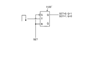
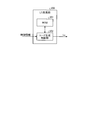
- FIG. 1 is a diagram showing a schematic configuration example of a light receiving device according to the first embodiment.
- the light receiving device 1a according to the first embodiment includes a pixel 10, a counting unit 11, a time code generation unit 12, and an acquisition unit 13.
- the light receiving device 1a counts the number of photons (photons) incident on the pixel 10 within the specified exposure period Tsh (for example, the shutter period). Based on the counted number of photons, it is possible to determine the illuminance during the exposure period Tsh.
- Pixel 10 converts the incident light into an electric signal by photoelectric conversion and outputs it. More specifically, the pixel 10 includes a photoelectric conversion element that converts light into an electric charge by photoelectric conversion, and a signal processing circuit that reads an electric charge from the photoelectric conversion element and outputs it as an electric signal. In the present disclosure, the pixel 10 converts photons (photons) incident on the photoelectric conversion element into an electric signal, and outputs pulses Vpls corresponding to the incident of the photons. In the present disclosure, a single photon avalanche diode is used as the photoelectric conversion element included in the pixel 10.
- SPAD Single Photon Avalanche Diode
- SPAD Single Photon Avalanche Diode
- SPAD has a characteristic that when a large negative voltage that causes avalanche multiplication is applied to the cathode, the electrons generated in response to the incident of one photon cause avalanche multiplication and a large current flows.
- the incident of one photon can be detected with high sensitivity.
- photons are incident on the photoelectric conversion element included in the pixel 10 is described as “photons are incident on the pixel 10.”
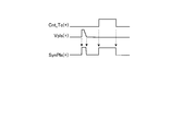
- the counting unit 11 counts the pulse Vpls output from the pixel 10 within the designated exposure period Tsh.
- the counting unit 11 starts counting the pulses Vpls, for example, at the start of the exposure period Tsh.
- the counting unit 11 outputs a write signal WRen instructing the writing of the number Nct of the measured pulse Vpls at a predetermined timing.
- the counting unit 11 outputs a write signal WRen instructing writing when the number Nct exceeds the threshold value Nth before the end of the exposure period Tsh. Further, for example, when the number Ncnt does not exceed the threshold value Nth even when the exposure period Tsh ends, the counting unit 11 outputs the write signal WRen instructing writing at the end point of the exposure period Tsh.
- the write signal WRen instructing writing will be described as the write signal WRen (W).
- the write signal WRen is supplied to the acquisition unit 13.
- the write signal WRen defaults to the low state, and by shifting from the low state to the high state, the acquisition unit 13 is instructed to write.
- the time code generation unit 12 generates a time code Tc that is initialized at the start timing of the exposure period Tsh and whose value changes in the cycle of the designated sampling frequency. For example, the time code generation unit 12 generates a time code Tc in which the value "0" is set as an initial value and the value increases by 1 for each cycle. The time code Tc generated by the time code generation unit 12 is supplied to the acquisition unit 13.
- the cycle of the designated sampling frequency at which the time code Tc is generated is, in other words, the cycle at which the time code Tc is updated.
- this cycle will be referred to as an update cycle.
- the acquisition unit 13 includes, for example, a memory, acquires the time code Tc supplied from the time code generation unit 12 at the timing when the write signal WRen shifts from the low state to the high state, and writes the acquired time code Tc to the memory. ..
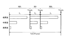
- FIG. 2A is a diagram showing an example of the relationship between the count value of the number of photons and time.
- the count value changes in a linear function with respect to time.
- Ct_m shows the time transition of the count value in the case of medium illuminance (medium illuminance).
- the straight line Ct_h indicating the time transition of the count value when the illuminance is higher than the medium illuminance (high illuminance) has a slope larger than that of the straight line Ct_m.
- the slope of the straight line Ct_l indicating the time transition of the count value when the illuminance is lower than the medium illuminance (low illuminance) is smaller than the straight line Ct_m.
- FIG. 2B is a diagram showing an example in which the threshold value Nth is added to the above-described FIG. 2A.
- the times when the count value reaches the threshold value Nth in high illuminance and medium illuminance are time Tth_h and time Tth_m, respectively. Since the count value has a linear function relationship with time, the count values of high illuminance and medium illuminance in the exposure period Tsh can be predicted based on the threshold value Nth and the time Tth_h and the time Tth_m. In the following, the predicted count values for high illuminance and medium illuminance will be referred to as predicted count values Npre_h and Npre_m, respectively.
- Npre Nth ⁇ (Tsh / Tth).
- Npre_h and Npre_m Nth ⁇ (Tsh / Tth_m)... (3)
- the straight line Ct_l has not reached the threshold value Nth within the exposure period Tsh.
- the count value at the end of the exposure period Tsh can be regarded as the predicted count value Npre_l based on the straight line Ct_l.
- counting by the counting unit 11 can be stopped.
- the counting by the counting unit 11 after the time when the count value reaches the threshold value Nth is stopped.
- the illuminance in the region (including) is medium illuminance
- the illuminance in the region between the straight line Ct_m and the X axis (time axis) is low illuminance.
- the straight line Ct_h in FIG. 2A and the time Tth_h in FIG. 2B indicate the boundary between the high illuminance and the medium illuminance
- the straight line Ct_m in FIG. 2A and the time Tth_m in FIG. Show boundaries.
- high illuminance is represented by a straight line Ct_h or time Tth_h
- medium illuminance is represented by a straight line Ct_m and time Tth_m.
- the predicted count values Npre_h and Npre_m represent the predicted count values Npre in high illuminance and medium illuminance, respectively.
- the acquisition unit 13 acquires the time Tth_h and the time Tth_m as the time code Tc from the time code generation unit 12 and writes them in the memory.
- the threshold value Nth and the exposure period Tsh are, for example, designated values and are fixed values. Therefore, by reading out the time Tth_h and the time Tth_m from the memory and executing the calculation in accordance with the above equation (1), the predicted count value Npre_h and the predicted count value Npre_m can be calculated.
- the time code generation unit 12 determines the update cycle according to the number of photons incident on the pixel 10 per unit time in the case of high illuminance. As a result, it is possible to count the number of photons in the case of high illuminance with high accuracy.
- the time code generation unit 12 changes the update cycle for generating the time code Tc, and changes the update cycle according to the elapsed time in the exposure period Tsh. More specifically, the time code generation unit 12 sets the shortest update cycle at the start time of the exposure period Tsh, and sets the update cycle with the passage of time from the start time to the end time of the exposure period Tsh. Lengthen. Thereby, the time interval in which the time code Tc changes can be lengthened with the passage of time in the exposure period Tsh.
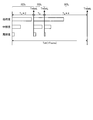
- FIG. 3 is a diagram for schematically explaining the generation of the time code Tc by the time code generation unit 12 according to the first embodiment.
- FIG. 3 from the top, the passage of time, an example of a count value in the case of low illuminance, an example of a count value in the case of high illuminance, an example of time code Tc in the case of equal intervals, and a time in the case of variable intervals.
- An example of the code Tc is shown respectively.
- the count value may not exceed the threshold value Nth within the exposure period Tsh.
- the count value may not exceed the threshold value Nth within the exposure period Tsh.
- the count value has not reached the threshold value Nth.
- the time code generation unit 12 generates the time code Tc at equal intervals according to a constant update cycle.
- the time code Tc is reset at the start of the exposure period Tsh, the time code Tc is generated at equal intervals as the exposure period Tsh elapses, and the time with the value "2047" at the end of the exposure period Tsh.
- Code Tc has been generated. That is, the counting unit 11 has a counter capable of counting 11 bits.
- the time code Tc corresponding to the time Tth is a value "11", and this value "11" is written to the memory by the acquisition unit 13.
- the time code Tc value "2047" at the end of the exposure period Tsh is written to the memory by the acquisition unit 13. Therefore, in the example of FIG. 3, when the time code generation unit 12 generates the time code Tc at equal intervals, the acquisition unit 13 needs a memory having a bit width of 11 bits.
- the time code generation unit 12 changes the update cycle as the exposure period Tsh elapses, and generates the time code Tc at variable intervals. At this time, the time code generation unit 12 generates the time code Tc by the shortest update cycle in the exposure period Tsh at the start of the exposure period Tsh. The update cycle is lengthened as the exposure period Tsh elapses, and at the end of the exposure period Tsh, the time code Tc is generated by the longest update cycle within the exposure period Tsh.
- the time code generation unit 12 classifies the illuminance into three stages of, for example, high illuminance, medium illuminance, and low illuminance, and the time code Tc at intervals according to different update cycles. That is, assuming that the update periods corresponding to high illuminance, medium illuminance, and low illuminance are update periods f h , f m, and f l , respectively, the relationship between these update periods f h , f m, and f l is f h >f m > a f l.
- the time code generation unit 12 generates a time code Tc at intervals according to the high illuminance update cycle f h from the start time of the exposure period Tsh to the first time point of the exposure period Tsh.
- the time code generation unit 12 generates a time code Tc at intervals according to the update cycle f m of medium illuminance from the first time point to the second time point when a predetermined time has elapsed. Further, the time code generation unit 12 generates the time code Tc at intervals according to the low illuminance update period f l from the second time point to the end time point of the exposure period Tsh.
- the time code generation unit 12 resets the time code Tc at the start of the exposure period Tsh, and sets the time code Tc values "1" to "8” to high illuminance. Values “9” to “16” are assigned to medium illuminance, and values "17" to “31” are assigned to low illuminance.
- the memory of the acquisition unit 13 may have, for example, a bit width of 5 bits.
- the time code Tc with respect to the time Tth is a value "8", and this value "8" is written to the memory by the acquisition unit 13.
- counting is continued until the end of the exposure period Tsh, but since the interval of the time code Tc is longer than in the case of high illuminance, the time at the end of the exposure period Tsh.
- the value "31" of the code Tc is written to the memory of the acquisition unit 13.
- the predicted count value Npre rapidly increases as the time Tth, which is the elapsed time from the start time of the exposure period Tsh, approaches 0, and the time Tth is further 0. In some cases it becomes infinite. Therefore, in the period when the time Tth is extremely short, the predicted count value Npre becomes an extremely large value, and the predicted count value Npre within the period becomes a value that does not make sense in reality. This means that the time code Tc in the period is unnecessary. Therefore, the time code generation unit 12 sets the shortest update cycle when a predetermined time elapses from the start time of the exposure period Tsh, and updates with the passage of time from that time toward the end time of the exposure period Tsh. It is preferable to lengthen the cycle.
- the predetermined time for setting the update cycle can be, for example, the time at which it is estimated that the predicted count value Npre corresponding to the predetermined illuminance (for example, the desired maximum illuminance) is obtained after the start of the exposure period Tsh. ..
- the time code Tc acquired when the number of photons detected by the pixel 10 in the exposure period Tsh reaches the threshold value Nth is obtained after the exposure period Tsh. It is generated at intervals according to the update cycle that changes with. Therefore, the bit width of the memory for writing the time code Tc can be kept small. As a result, the circuit area can be reduced.
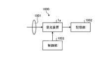
- FIG. 4 is a block diagram schematically showing the configuration of an example of an electronic device to which the light receiving device 1a according to the first embodiment is applied.
- the electronic device 1000 includes an optical system including a lens 1001, a light receiving device 1a, a storage unit 1002, and a control unit 1003.
- the optical system guides the light incident on the lens 1001 to the light receiving surface of the pixel 10 in the light receiving device 1a.
- the storage unit 1002 includes a storage medium that stores data, such as a memory, and a control unit that controls reading and writing with respect to the storage medium.
- the storage unit 1002 stores the output data output from the light receiving device 1a.
- the control unit 1003 controls the light receiving device 1a to execute the operation of causing the light receiving device 1a to output the above-mentioned output data. For example, the control unit 1003 can instruct the light receiving device 1a of the start time point and the end time point (the length of the exposure period Tsh) of the exposure period Tsh. Further, for example, the control unit 1003 can output a reference signal for the update cycle for generating the time code Tc to the light receiving device 1a. Further, for example, the control unit 1003 can instruct the light receiving device 1a of the timing for switching the interval of the time code Tc between high illuminance, medium illuminance, and low illuminance.
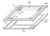
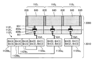
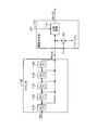
- FIG. 5 is a schematic diagram showing an example of a device configuration applicable to the light receiving device 1a according to the first embodiment.
- the light receiving device 1a is configured by stacking a light receiving chip 2000, which is a semiconductor chip, and a logic chip 2010, respectively. Note that in FIG. 5, the light receiving chip 2000 and the logic chip 2010 are shown in a separated state for the sake of explanation.
- the light receiving chip 2000 includes a pixel array unit 2001 in which a plurality of photoelectric conversion elements 110 included in a plurality of pixels 10 on a one-to-one basis are arranged, for example, in a two-dimensional lattice pattern.
- the logic chip 2010 is provided with a logic array unit 2011 including a signal processing unit that processes a signal acquired by the photoelectric conversion element 110.
- Each circuit included in the light receiving chip 2000 and each circuit included in the logic chip 2010 are electrically connected by a CCC (Copper-Copper Connection) or the like.
- a storage unit 2012 that stores a signal acquired by the photoelectric conversion element 110 in close proximity to the logic array unit 2011, and an element control unit 2013 that controls the operation as the light receiving device 1a. , Can be provided.
- a part of the wiring included in the wiring layer of the light-receiving chip 2000 and a part of the wiring included in the wiring layer of the logic chip 2010 are directly bonded to each other, so that the light-receiving chip 2000 and the logic chip are connected.
- the wiring in this case can be formed of a conductive material such as metal, using copper as an example.
- connection form between the light receiving chip 2000 and the logic chip 2010 is not limited to CCC.
- the light receiving chip 2000 and the logic chip 2010 can be connected by a bump connection, a through electrode, or the like.
- the electrical connection between the light receiving chip 2000 and the logic chip 2010 is performed, for example, by transmitting a pixel signal generated by the light receiving chip 2000 to the logic chip 2010 or in the light receiving chip 2000 of a power source applied from the outside.
- the purpose is to supply the logic chip 2010.
- the power applied from the outside is supplied to the wiring layer of the light receiving chip 2000 via a bonding pad (leading electrode) provided outside the pixel array section 2001 in the light receiving chip 2000, for example.
- the wiring layer of the light receiving chip 2000 and the wiring layer of the logic chip 2010 are directly connected by the connection portion such as the CCC described above, and power is supplied from the light receiving chip 2000 to the logic chip 2010.
- connection portion for making an electrical connection between the light receiving chip 2000 and the logic chip 2010 is provided for each pixel 10, but this is an example of this example. Not limited. For example, a configuration in which one connection portion is provided for a plurality of pixels 10 or a configuration in which a plurality of connection portions are provided for one pixel 10 may be used.
- the element control unit 2013 can be arranged for other driving or control purposes, for example, in the vicinity of the photoelectric conversion element 110, in addition to the control of the logic array unit 2011.
- the element control unit 2013 can be provided in an arbitrary region of the light receiving chip 2000 and the logic chip 2010 so as to have an arbitrary function.
- the photoelectric conversion element 110 among the elements included in the pixel 10 is arranged on the light receiving chip 2000, but this is not limited to this example. That is, a signal processing circuit that converts the electric charge read from the photoelectric conversion element 110 into an electric signal may be further arranged on the light receiving chip 2000. Furthermore, a circuit for performing other signal processing on the electric signal output from the signal processing circuit may be arranged for the light receiving chip 2000.
- FIG. 6 is a plan view showing the configuration of an example of the light receiving chip 2000 applicable to the first embodiment.
- the light receiving chip 2000 is provided with a pixel array unit 2001, and the pixel array unit 2001 is provided with a plurality of photoelectric conversion elements 110 in a two-dimensional lattice pattern. Details of the photoelectric conversion element 110 will be described later.
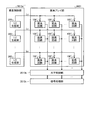
- FIG. 7 is a block diagram showing a configuration of an example of logic chip 2010 applicable to the first embodiment.
- a vertical control unit 2013a, a logic array unit 2011, a horizontal control unit 2013b, a signal processing unit 2013c, and a storage unit 2012 are arranged on the logic chip 2010.
- the vertical control unit 2013a, the horizontal control unit 2013b, and the signal processing unit 2013c can be configured to be included in the element control unit 2013.
- logic circuits 2014 are arranged for each photoelectric conversion element 110.
- Each of these logic circuits 2014 is connected to the corresponding photoelectric conversion element 110 via a signal line.
- the circuit including the photoelectric conversion element 110 and the logic circuit 2014 corresponding to the photoelectric conversion element 110 functions as a pixel circuit that generates a pixel signal by one pixel 10.
- the vertical synchronization signal and the horizontal synchronization signal output from the control unit 1003 are supplied to the vertical control unit 2013a and the horizontal control unit 2013b, respectively. Further, the exposure control signal output from the control unit 1003 is supplied to the logic array unit 2011 and the signal processing unit 2013c, respectively.
- the predetermined direction of the two-dimensional lattice (for example, the horizontal direction in FIGS. 6 and 7) is the row direction, and the direction perpendicular to the row is the column direction. That is, the pixel circuits (photoelectric conversion element 110 and logic circuit 2014) are arranged and arranged in the row direction and the column direction with respect to the pixel array unit 2001 and the logic array unit 2011, respectively.
- a set of pixel circuits in the row direction is referred to as a “row”, and a set of pixel circuits in the column direction is referred to as a “column”.
- the vertical control unit 2013a selects rows in order in synchronization with the vertical synchronization signal.
- the logic circuit 2014 includes the counting unit 11 and the acquisition unit 13 described with reference to FIG. 1, and can output the time code Tc stored in the memory of the acquisition unit 13.
- the time code Tc output from each logic circuit 2014 is supplied to the signal processing unit 2013c.
- the horizontal control unit 2013b outputs a pixel signal by sequentially selecting columns in synchronization with the horizontal synchronization signal.
- the signal processing unit 2013c further receives information (exposure start timing, exposure time, etc.) indicating the exposure period Tsh from the control unit 1003.
- the signal processing unit 2013c calculates the predicted count value Npre based on each time code Tc supplied from each logic circuit 2014, for example, according to the above-mentioned equation (1).
- the signal processing unit 2013c outputs each calculated predicted count value Npre.
- Each predicted count value Npre output from the signal processing unit 2013c is supplied to and stored in the storage unit 2012.
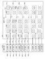
- FIG. 8 is a block diagram showing a configuration of an example of the pixel array unit 2001 and the vertical control unit 2013a according to the first embodiment. Further, in FIG. 8, a more specific configuration of the pixel circuit is shown with respect to the pixel array unit 2001.
- the pixel array unit 2001 includes a plurality of pixel circuits 100a. Note that FIG. 8 shows an excerpt of each pixel circuit 100a included in one line among the pixel circuits 100a arranged in a two-dimensional grid pattern in the pixel array unit 2001.
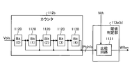
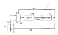
- the pixel circuit 100a includes a photoelectric conversion element 110, a signal processing unit 111a, a counter 112, a threshold value determination unit 113a, and a memory 114.
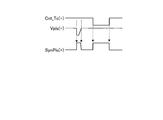
- the photoelectric conversion element 110 outputs a signal Vph according to the incident of photons.
- the signal Vph is transmitted from the light receiving chip 2000 to the logic chip 2010 via a coupling unit by CCC, for example, and is supplied to the signal processing unit 111a arranged in the logic chip 2010.
- the signal processing unit 111a shapes the signal Vph output from the photoelectric conversion element 110 and outputs it as pulses Vpls according to the incident of photons.
- the output timing of the pulse Vpls is controlled according to the signal SH_ON supplied from the TC generator 120 described later.
- the counter 112 counts the number of pulses Vpls output from the signal processing unit 111a, and outputs the count result as photon information PhInfo.
- the threshold value determination unit 113a makes a determination based on the threshold value Nth with respect to the photon information PhInfo output from the counter 112.
- the threshold value determination unit 113a determines that the number of photons incident on the photoelectric conversion element 110 exceeds the threshold value Nth based on the photon information PhInfo
- the threshold value determination unit 113a outputs a write signal WRen (W).
- the counter 112 and the threshold value determination unit 113a constitute the counting unit 11 of FIG.
- the memory 114 corresponds to the acquisition unit 13 in FIG. 1 and stores the time code Tc supplied from the TC generation unit 120, which will be described later, via the signal line 142 in accordance with the write signal WRen.
- the memory 114 includes a memory control unit that controls writing data to the memory 114 itself and reading data from the memory 114.
- the vertical control unit 2013a includes a TC (time code) generation unit 120 for each line.
- the TC generation unit 120 corresponds to the time code generation unit 12 shown in FIG.
- the TC generation unit 120 generates an update cycle that changes with the passage of the exposure period Tsh under the control of the control unit 1003, and generates a time code Tc based on this update cycle.
- the control unit 1003 generates a reference timing signal and supplies it to the TC generation unit 120.
- the TC generation unit 120 generates the time code Tc at a predetermined update cycle based on this reference timing signal.
- the time code Tc generated by the TC generation unit 120 is input to the pixel circuits 100a, 100a, ... Via the signal line 142, and is input to the memory 114 of each pixel circuit 100a, 100a, ... Each is supplied and stored.
- Each time code Tc stored in the memory 114 of each pixel circuit 100a, 100a, ... Is read from each memory 114 via the signal line 142.
- control unit 1003 instructs, for example, the start timing of the exposure period Tsh to the TC generation unit 120 and supplies information indicating the length of the exposure period Tsh to the TC generation unit 120.
- the TC generation unit 120 generates a signal SH_ON instructing the timing at which the signal processing unit 111a outputs the pulse Vpls.
- the TC generation unit 120 generates the signal SH_ON based on, for example, a predetermined clock signal.
- the signal SH_ON generated by the TC generation unit 120 is input to the pixel circuits 100a, 100a, ... Via the signal line 141, and is supplied to the signal processing unit 111a.
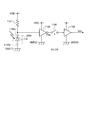
- FIG. 9 is a diagram showing a configuration of an example of the signal processing unit 111a applicable to the first embodiment.
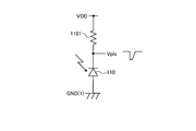
- the signal processing unit 111a includes a resistor 1101, an inverter 1102, an amplifier 1103, and a switch 1104.
- the cathode is connected to the terminal of the power supply potential VDD via the resistor 1101, and the anode is connected to the terminal of the potential GND (1) whose potential is lower than the power supply potential VDD.
- the terminal of the potential GND(1) is, for example, a ground terminal.
- the photoelectric conversion element 110 is not limited to SPAD. It is also possible to apply an avalanche photodiode (APD) or a normal photodiode as the photoelectric conversion element 110.
- APD avalanche photodiode
- APD normal photodiode
- One end of the resistor 1101 is connected to the power potential VDD, and the other end is connected to the cathode of the photoelectric conversion element 110. Every time the incident of photons is detected in the photoelectric conversion element 110, a photocurrent flows through the resistor 1101, and the cathode potential of the photoelectric conversion element 110 drops to a value in the initial state lower than the power supply potential VDD (quenching operation).
- a signal extracted from the connection point between the resistor 1101 and the cathode of the photoelectric conversion element 110 is input to the inverter 1102.
- the inverter 1102 inverts the input signal of the cathode potential of the photoelectric conversion element 110, and supplies the inverted output signal Vsig to the amplifier 1103 via the switch 1104.
- the amplifier 1103 shapes the inverted output signal Vsig and outputs it as pulses Vpls.
- the ground-side potential GND (2) to which the inverter 1102 and the amplifier 1103 are connected is different from the ground-side potential GND (1) to which the anode of the photoelectric conversion element 110 is connected.
- the photoelectric conversion element 110 is formed on the light receiving chip 2000.
- the resistor 1101, the inverter 1102, the amplifier 1103, and the switch 1104 are formed on the logic chip 2010.
- the cathode of the photoelectric conversion element 110 is connected to a connection point where the resistor 1101 and the input end of the inverter 1102 are connected via, for example, a coupling portion 1105a formed by CCC.
- the anode of the photoelectric conversion element 110 is connected to a supply line that supplies the ground-side potential (1) arranged on the logic chip 2010 via, for example, a coupling portion 1105b by CCC.
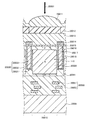
- FIG. 10A is a diagram showing an example of a configuration of a photoelectric conversion element 110 as a SPAD applicable to the first embodiment.
- the photoelectric conversion element 110 includes a multiplication region as a SPAD pixel using SPAD and a photoelectric conversion unit (N ⁇ region) 840 that performs photoelectric conversion, and the outermost surface on the back surface side of the photoelectric conversion unit 840 is It is used as a light irradiation unit that is irradiated with light.
- an anode electrode (not shown) is electrically connected to the P-type semiconductor region 760.
- the P-type semiconductor region 760 is configured so that the lower layer has a lower impurity concentration.
- the P-type semiconductor region 700 and the P ⁇ type semiconductor region 710 are formed from the P-type semiconductor region 760 along the pixel isolation portion 831 including the metal layer 830, and the P-type semiconductor region 760 to the avalanche portion 720 are electrically connected. It is connected to the.
- the avalanche portion 720 is configured by joining a P+ type semiconductor region 730 and an N+ type semiconductor region 740.
- the P-type semiconductor region 700 is configured by accumulating opposite charges (holes) so that the charges (electrons) to be read by the avalanche unit 720 pass through.
- the P-type semiconductor region 710 is preferably a low-concentration region in order to raise the central potential so that the electric charge passes through the avalanche portion 720.
- the N + type semiconductor region 740 is connected to the electrode 801 via the N + type semiconductor region 750. Further, an N ⁇ type semiconductor region 780 is formed on the side surfaces of the P + type semiconductor region 730 and the N + type semiconductor region 740. Further, a P + type semiconductor region 790 that is electrically connected to the N + type semiconductor region 740 and the N ⁇ type semiconductor region 780 is provided, and the P + type semiconductor region 790 is grounded (GND) via the electrode 800.
- a fixed charge film 810 is provided on the side surface of the pixel separation portion 831 and the upper layer of the P-type semiconductor region 760.
- a color filter 822 is provided on the fixed charge film 810 via an insulating film 821.
- An on-chip lens 820 is provided above the color filter 822.
- the color filter 822 is provided according to the application.
- FIG. 10B is a diagram showing an example of the configuration of the light receiving unit 2010 including the photoelectric conversion element 110 as a photodiode, which can be applied to the first embodiment.
- the photoelectric conversion element 110 which is a photodiode, receives incident light 20001 incident from the back surface (upper surface in FIG. 10B) side of the semiconductor substrate 20018.
- a flattening film 2013, a color filter 2001, and a microlens 20011 are provided above the photoelectric conversion element 110, and incident light 20001 incident through each part is received by the light receiving surface 200017 to perform photoelectric conversion. Be seen.
- the N-type semiconductor region 20020 is formed as a charge storage region for accumulating charges (electrons).
- the N-type semiconductor region 20020 is provided inside the P-type semiconductor region 2016, 20041 of the semiconductor substrate 20018.
- the front surface (lower surface) side of the semiconductor substrate 20018 of the N-type semiconductor region 20020 is provided with a P-type semiconductor region 20044 having a higher impurity concentration than the back surface (upper surface) side. That is, the photoelectric conversion element 110 has a HAD (Hole-Accumulation Diode) structure, so as to suppress the generation of dark current at each interface between the upper surface side and the lower surface side of the N-type semiconductor region 20020.
- HAD Hole-Accumulation Diode
- a pixel separation unit 20030 that electrically separates the plurality of light receiving units 20010 is provided inside the semiconductor substrate 20018, and the photoelectric conversion element 110 is provided in a region partitioned by the pixel separation unit 20030. ing.
- the pixel separation unit 20030 is formed in a grid shape so as to be interposed between a plurality of light receiving units 2001, and the photoelectric conversion element 110 is It is formed in the region partitioned by the pixel separation unit 20030.
- each photoelectric conversion element 110 the anode is grounded, and the signal charge (eg, electrons) accumulated in the photoelectric conversion element 110 in the light receiving unit 20010 is not shown by, for example, a MOSFET (Metal Oxide Semiconductor Field Effect Transistor). It is read out via a transfer transistor or the like and output as an electric signal to a VSL (vertical signal line) (not shown).
- MOSFET Metal Oxide Semiconductor Field Effect Transistor
- the wiring layer 20050 is provided on the front surface (lower surface) of the semiconductor substrate 20018, which is opposite to the back surface (upper surface) on which the light shielding film 20014, the color filter 20012, the microlens 20011, and the like are provided.
- the wiring layer 20050 includes the wiring 20051 and the insulating layer 20052, and is formed so that the wiring 20051 is electrically connected to each element in the insulating layer 20052.
- the wiring layer 20050 is a layer of so-called multi-layer wiring, and is formed by alternately laminating the interlayer insulating film constituting the insulating layer 20052 and the wiring 20051 a plurality of times.
- wiring 20051 wiring to a transistor for reading charge from a photoelectric conversion element 110 such as a transfer Tr, and wiring such as VSL are laminated via an insulating layer 20052.
- a support substrate 20061 is provided on the surface of the wiring layer 20050 opposite to the side on which the photoelectric conversion element 110 is provided.
- a substrate made of a silicon semiconductor having a thickness of several hundred ⁇ m is provided as a support substrate 20061.
- the light-shielding film 2014 is provided on the back surface side (upper surface in the figure) of the semiconductor substrate 20018.
- the light-shielding film 2014 is configured to block a part of the incident light 20001 directed from above the semiconductor substrate 20018 toward the back surface of the semiconductor substrate 20018.
- the light-shielding film 20014 is provided above the pixel separation unit 20030 provided inside the semiconductor substrate 20018.
- the light-shielding film 2014 is provided on the back surface (upper surface) of the semiconductor substrate 20018 so as to project in a convex shape via an insulating film 2015 made of a silicon oxide film or the like.
- the light shielding film 20014 is not provided and is opened so that the incident light 20001 enters the photoelectric conversion element 110. ing.
- the planar shape of the light shielding film 2014 is a grid pattern that partitions the plurality of light receiving portions 20010, and the incident light 20001 passes through the light receiving surface 200017. An opening is formed.
- the light-shielding film 2014 is formed of a light-shielding material that blocks light.
- the light-shielding film 2014 is formed by sequentially laminating a titanium (Ti) film and a tungsten (W) film.
- the light-shielding film 2014 can be formed, for example, by sequentially laminating a titanium nitride (TiN) film and a tungsten (W) film.
- the light shielding film 20014 is covered with the planarization film 20013.
- the flattening film 2013 is formed by using an insulating material that transmits light.
- the pixel separation section 20030 has a groove section 20031, a fixed charge film 20032, and an insulating film 20033.
- the fixed charge film 20032 is formed on the back surface (upper surface) side of the semiconductor substrate 20018 so as to cover the groove portion 20031 partitioning between the plurality of light receiving portions 20010. Specifically, the fixed charge film 20032 is provided so as to cover the inner surface of the groove portion 20033 formed on the back surface (upper surface) side of the semiconductor substrate 20018 with a constant thickness. An insulating film 20033 is provided (filled) so as to fill the inside of the groove 20031 covered with the fixed charge film 20032.
- the fixed charge film 20032 is made of a high dielectric material having a negative fixed charge so that a positive charge (hole) accumulation region is formed at the interface with the semiconductor substrate 20018 and the generation of dark current is suppressed. Is formed. Since the fixed charge film 20032 is formed so as to have a negative fixed charge, an electric field is applied to the interface with the semiconductor substrate 20018 by the negative fixed charge, and a positive charge (hole) storage region is formed.
- the fixed charge film 20032 can be formed of, for example, a hafnium oxide film (HfO 2 film).
- the fixed charge film 20032 can be formed so as to contain at least one of other oxides such as hafnium, zirconium, aluminum, tantalum, titanium, magnesium, yttrium, and lanthanoid elements.
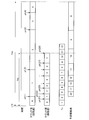
- FIG. 11 is a block diagram showing a configuration of an example of the TC generation unit 120 according to the first embodiment.
- FIG. 12 is an example timing chart for explaining the operation of the TC generation unit 120 according to the first embodiment.
- the TC generation unit 120 includes a time counter 121, a frequency division set value storage unit 122, a frequency determination unit 123, and a code generation unit 124.
- the time counter 121 is driven at a constant frequency and counts, for example, the reference clock signal supplied from the control unit 1003.
- the time counter 121 counts the reference clock signal by, for example, initializing the count value to "0" at the start of the exposure period Tsh, increasing the count value by "1" at the rising or falling edge of the reference clock signal. ..
- the exposure period Tsh has a length of 128 counts of the reference clock signal.
- the count value of the time counter 121 is "0" at the start of the exposure period Tsh and "127" at the end.
- the frequency division set value storage unit 122 stores a plurality of frequency division values in advance, and outputs the frequency division value required from the stored frequency division values in response to the request of the frequency determination unit 123. .. As an example, the frequency division set value storage unit 122 stores the values "31", "63", and "127" as the frequency frequency division value.
- the frequency determination unit 123 inputs the count value of the time counter 121 and the frequency division value output from the frequency division set value storage unit 122.
- the frequency determination unit 123 outputs frequency information based on the input count value and frequency frequency division value.
- the initial value of the frequency information is “1”.
- the frequency determination unit 123 determines whether or not the input count value and the frequency division value match. If it is determined that the count value and the frequency division value match and the currently input frequency division value is not the maximum value, the frequency determination unit 123 adds 1 to the frequency information. And output. At the same time, the frequency determination unit 123 requests the frequency division set value storage unit 122 for a frequency division value that is one larger than the currently input frequency division value.
- the code generation unit 124 outputs the time code Tc based on the reference clock signal and the frequency information output from the frequency determination unit 123. At this time, the code generation unit 124 divides the reference clock signal by the number of times according to the frequency information to change the update cycle, and controls the time interval of the time code Tc. For example, the code generation unit 124 frequency-divides the reference clock signal once when the value of the frequency information is “1”, and generates the time code Tc according to the half of the update cycle of the reference clock signal. Further, for example, the code generation unit 124 divides the reference clock signal twice with the value of the frequency information being “2”, and generates the time code Tc in accordance with the 1/4 update cycle of the reference clock signal.
- the clock shows a count value obtained by counting the reference clock signal by the time counter 121.
- the clock value is set to "0" at the start of the exposure period Tsh and "127" at the end.
- the frequency determination unit 123 acquires the value “31” which is the initial value of the frequency division value from the frequency division setting value storage unit 122, and the value “1” which is the initial value of the frequency information. Is output.
- the code generation unit 124 divides the reference clock signal once based on the frequency information of the value "1", and sets a time code Tc whose value increases by 1 according to the frequency (update cycle) of 1/2 of the reference clock signal. Generate.
- the frequency determination unit 123 determines that the clock value matches the frequency fractional value “31”
- the frequency setting unit 122 stores a frequency that is one greater than the current frequency fractional value “31”. Request the frequency division value "63”.
- the frequency determination unit 123 adds "1" to the value "1" of the frequency information to obtain the value "2".
- the code generator 124 divides the reference clock signal twice according to the value “2” of the frequency information, and generates the time code Tc whose value increases by 1 according to the frequency of 1 ⁇ 4 of the reference clock signal.
- the code generation unit 124 sets the value “0” according to the half frequency of the reference clock signal during the period when the frequency information has the value “1” (clock values “0” to “31”). To the value “15” are incremented by one, the time code Tc is sequentially generated. When the frequency information switches from the value “1” to the value “2”, the code generation unit 124 generates the time code Tc that increases by 1 from the next value “16” according to the frequency of 1 ⁇ 4 of the reference clock signal. ..
- each time the clock value matches the frequency division value the division ratio for dividing the reference clock signal is increased and the frequency division is performed.
- the peripheral price is being updated. Therefore, the update cycle is sequentially lengthened according to the passage of time in the exposure period Tsh, and the time interval of the time code Tc is sequentially lengthened.
- the time code Tc'generated at a fixed time interval within the exposure period Tsh is used.
- the time code Tc' is generated according to a frequency of 1/2 of the frequency of the reference clock signal.
- the time code Tc'at the end of the exposure period Tsh has a value of "63", which is 6-bit data.
- the time code Tc at the end of the exposure period Tsh becomes the value “31”, which is 5 bits. It becomes the data of.
- the time interval of the time code Tc variable, the number of bits of the time code Tc can be reduced, and the size of the memory for storing the time Tth acquired by the time code Tc can be reduced.
- the period in which the division ratio to the reference clock signal is the smallest (1/2) is the period in which the time code Tc is generated according to the shortest update period, and the time Tth when the number of incident photons reaches the threshold value Nth is calculated. , Can be obtained with the highest accuracy.
- the division ratio becomes larger, the update cycle for generating the time code Tc becomes longer, and the acquisition accuracy of the time Tth becomes lower.
- the time Tth can be efficiently obtained by making the time interval of the time code Tc the shortest at the start of the exposure period Tsh and gradually increasing the time interval of the time code Tc as the exposure period Tsh elapses. Become. Further, since it is possible to set an appropriate time interval of the time code Tc for high illuminance, medium illuminance, and low illuminance, it is possible to suppress quantization noise.
- the time counter 121 is driven at a constant frequency to count the reference clock signal, but this is not limited to this example.
- the frequency that drives the time counter 121 may be variable.
- FIG. 13 is an example timing chart for explaining the operation of the TC generation unit 120 when the frequency for driving the time counter 121 is variable according to the first embodiment. Since the meaning of each part of the timing chart of FIG. 13 is the same as that of the timing chart of FIG. 12 described above, the description thereof will be omitted here.
- the time counter 121 is driven with a clock value of "32" or later and a frequency halved before that.
- the frequency frequency division values stored in the frequency division set value storage unit 122 are set to the values "31", "47", and "63".
- the operations of the frequency determination unit 123 and the code generation unit 124 are the same as those in FIG. 12 described above. Even in this case, the time interval of the time code Tc can be made variable based on the frequency division value and the frequency information, and the number of bits of the time code Tc can be reduced.
- a numerical value that increases by 1 is applied as the time code Tc, but this is not limited to this example. That is, the increment of the time code Tc is not limited to 1. Furthermore, if the values do not overlap, a value other than simple increase or simple decrease may be used for the time code Tc.
- FIG. 14 is a timing chart showing an example in which the Gray code is applied to the time code Tc as an example of values other than simple increase or simple decrease, which can be applied to the first embodiment. Since the meaning of each part of the timing chart of FIG. 14 is the same as that of the timing chart of FIG. 12 described above, the description thereof will be omitted here. Further, FIG. 14 shows an excerpt of the period in which the frequency division value in FIG. 12 is the value “31”.
- the Gray code is a code in which the Hamming distance between the adjacent codes is always 1, and has a characteristic that only 1 bit always changes when changing from a certain value to an adjacent value.
- the Gray code is a code in which the Hamming distance between the adjacent codes is always 1, and has a characteristic that only 1 bit always changes when changing from a certain value to an adjacent value.
- the frequency determination unit 123 generates frequency information for the code generation unit 124 to generate the time code Tc based on the frequency division value and the count value of the time counter 121.
- the frequency information may be generated using a PLL (Phase Locked Loop).
- FIG. 15 is a block diagram showing an example of a configuration for generating a time code Tc using a PLL, which is applicable to the first embodiment.
- the TC generation unit 120 ′ includes a frequency division setting value storage unit 122, a clock generation unit 125, a PLL circuit 126, and a code generation unit 127. Similar to the TC generation unit 120 shown in FIG. 11, the frequency division set value storage unit 122 stores a plurality of frequency frequency division values (for example, the values “31”, “63” and “127”) in advance.
- the clock generation unit 125 generates a clock signal having a stable frequency based on, for example, a reference clock signal supplied from the control unit 1003.
- the clock signal generated by the clock generation unit 125 and the frequency division value output from the frequency division set value storage unit 122 in response to the request of the PLL circuit 126 are input.
- the PLL circuit 126 generates a clock signal having a frequency corresponding to the frequency division value based on the input clock signal.
- the clock signal generated by the PLL circuit 126 is supplied to the code generation unit 127.
- the code generation unit 127 includes, for example, a counter and a comparison unit.
- the counter counts the clock signal supplied from the PLL circuit 126.
- the comparison unit compares the count value counted by the counter with the threshold value Nth. When the code generation unit 127 determines that the count value is equal to or higher than the threshold value Nth, the code generation unit 127 outputs the count value as a time code Tc.
- the code generation unit 127 determines that the count value is equal to or higher than the threshold value Nth and the currently input frequency frequency division value is not the maximum value, the code generation unit 127 currently refers to the frequency division setting value storage unit 122. Request a frequency division value that is one higher than the input frequency division value. As a result, the frequency of the clock signal generated by the PLL circuit 126 can be lowered. At this time, by controlling the clock signal for generating the time code Tc by the PLL circuit 126, finer control of the time code Tc becomes possible.
- 16A and 16B are block diagrams showing an example of the configuration of the counter 112a of the first example applicable to the first embodiment.
- the threshold value Nth is set to the value "31" in decimal notation and the value "0b11111" in binary notation. In the binary notation, the leading character string “0b” indicates that the subsequent character string (“11111” in this example) is a value in binary notation.
- the counter 112a includes a plurality of counters 1120, 1120, ..., Each of which counts 1 bit.
- the counters 1120, 1120, ... Have a configuration in which T (toggle) flip-flops (hereinafter, abbreviated as T-FF) are connected in series.
- the counter 112a in which each counter 1120 counts bits can be configured.
- the counter 112a in the counter 112a, five counters 1120 are connected in series, so that the counter 112a has bits from "0" (Bit (0)) to "4" (Bit (4)). It operates as a 5-bit counter.
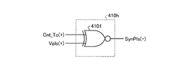
- the threshold determination unit 113a (a) includes, for example, a 1-bit counter 1130, and when a value “1” is input from the counter 112a, 1 bit is output from the counter 1130 and the number of incident photons reaches the threshold Nth. Therefore, the write signal WRen(W) to the memory 114 is output.
- FIG. 17 is a block diagram showing the configuration of an example of the counter 112b of the second example applicable to the first embodiment.
- counters 112b are connected in series with counters 1120, 1120, ... By T-FF, respectively.
- the counter 112b is output from the output terminals Q of the counters 1120, 1120, ..., And each of the extracted bits is output as a bit string.
- the counter 112b since the counter 112b includes five counters 1120, it is output as a 5-bit bit string.
- the bit string output from the counter 112b is supplied to the threshold value determination unit 113a (b) as photon information PhInfo.
- the threshold value determination unit 113a (b) corresponds to the threshold value determination unit 113a in FIG. 8 and includes the comparison circuit 1131.
- the photon information PhInfo supplied to the threshold value determination unit 113a(b) is input to the comparison circuit 1131.
- the comparison circuit 1131 compares the input photon information PhInfo with the threshold value Nth, and outputs a write signal WRen(W) to the memory 114 when the value indicated by the photon information PhInfo and the threshold value Nth match. To do.
- the counter 112b and the threshold value determination unit 113a (b) of this second example it is possible to set an arbitrary value within the range of the number of bits corresponding to the number of counters 1120 as the threshold value Nth.
- FIG. 18 is a block diagram showing an example of the configuration of the counter 112c of the third example applicable to the first embodiment.
- the counter 112c according to the third example is connected in series with counters 1120, 1120, ... By T-FF, respectively.
- the counter 112c outputs three signals, which are the input and output of the counter 1120 corresponding to the MSB and the pulse Vpls input to the counter 112c, as photon information PhInfo.
- the photon information PhInfo output from the counter 112c is supplied to the threshold value determination unit 113a (c) corresponding to the threshold value determination unit 113a in FIG.
- the threshold value determination unit 113a (c) includes a 3-input AND circuit 1132.
- the three signals included in the photon information PhInfo input to the threshold value determination unit 113a (c) are input to the three input terminals of the AND circuit 1132.
- the threshold value determination unit 113a(c) outputs the write signal WRen(W) to the memory 114 when the three values included in the photon information PhInfo become “1”. Since the pulse Vpls input to the counter 112c is used as the determination condition based on the logical product, the write signal WRen can be output in synchronization with the input of the pulse Vpls.
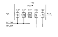
- FIGS. 19A and 19B are block diagrams showing an example of the configuration of the counter 112d of the fourth example applicable to the first embodiment.
- the counters 112d are connected in series with counters 1120', 1120', ..., which are asynchronous T-FFs (hereinafter, SRT-FFs), respectively.
- SRT-FF makes it possible to determine the initial state by a control signal from the outside.
- Each counter 1120' which is an SRT-FF, has a terminal S and a terminal R in addition to the input terminal T, as shown in FIG. 19B.
- the signal SET is input to the terminal R and is inverted and input to the terminal S.
- the signal RST_CNT is input as the above-mentioned signal SET to the three counters 1120'(Bit (0), Bit (1) and Bit (2)) on the LSB (Least Significant Bit) side. .. Further, the signal SET_CNT is input as the above-mentioned signal SET to the two counters 1120'(Bit (3) and Bit (4)) on the MSB side. For example, when resetting the counters 1120', 1120', ..., Which are included in the counter 112d, the signal RST_CNT is set to the value "0" and the signal SET_CNT is set to the value "1" as the initialization process.
- the threshold value Nth can be controlled by initializing the counters 1120', 1120',... In this way.
- the counter 112d is input by inputting eight pulses Vpls. Overflows and the photon information PhInfo having the value “1” is output. That is, in this case, the threshold value Nth is controlled to the value “8”.
- FIG. 20 is a block diagram showing an example of the configuration of the counter 112e of the fifth example applicable to the first embodiment.
- the counters 112e are connected in series with counters 1120', 1120', ..., Which are asynchronous T-FFs (hereinafter, SRT-FFs), respectively.
- SRT-FFs asynchronous T-FFs
- Each bit of the 5-bit signal INIT_CNT_DATA is input via switches 1121, 1121, ... As the signal SET described with reference to FIG. 19B, respectively.
- Each switch 1121 is simultaneously controlled on (closed) and off (open) by a 1-bit signal INIT_CNT.
- each bit of the signal INIT_CNT_DATA By setting each bit of the signal INIT_CNT_DATA to, for example, a value “0” and turning on each switch 1121 at a predetermined timing by the signal INIT_CNT, the value “0” is written to each counter 1120′, 1120′,... 1120′, 1120′,... Can be reset.
- FIG. 21 is a diagram showing a configuration of an example of counters 112f 1 , 112f 2 and 112f 3 of a sixth example applicable to the first embodiment. Any of the counters 112a to 112e described above may be applied to these counters 112f 1 , 112f 2 and 112f 3 .
- FIG. 21 In the example of FIG. 21, three photoelectric conversion elements 110 1 , 110 2 and 110 3 are shown.
- the pixel separation unit 831 and the photoelectric conversion unit 840 are excerpted from the configuration shown in FIG.
- these photoelectric conversion elements 110 1 , 110 2 and 110 3 are arranged on light receiving chip 2000.
- the counters 112f 1 , 112f 2 and 112f 3 are arranged on the logic chip 2010.
- the photoelectric conversion elements 110 1 , 110 2 and 110 3 on the light receiving chip 2000 are connected to the connection portion 850a of the light receiving chip 2000 via the electrode 801'.
- the connection portion 850a is connected to the connection portion 850b in the logic chip 2010 by, for example, CCC.
- the counters 112f 1 , 112f 2 and 112f 3 are connected to the connecting portions 850b via the corresponding electrodes 851.
- each signal Vph output by the photoelectric conversion elements 110 1 , 110 2 and 110 3 in response to the incident of photons is sent to each counter 112f via the electrodes 801', the connecting portions 850a and 850b, and the electrodes 851. 1 , 112f 2 and 112f 3 .
- the counter 112a shown in FIG. 16A is applied as each of the counters 112f 1 , 112f 2, and 112f 3 . Further, it is assumed that the counters 112f 1 , 112f 2 and 112f 3 are 6-bit counters including 6 counters 1120 (Bit (0)) to 1120 (Bit (5)), respectively.
- Counters 1120 (Bit (0)), 1120 (Bit (1)), 1120 (Bit (2)) and 1120 (Bit (3)) are collectively referred to as counters 1120a 1 , 1120a 2 and 1120a 3 .
- 1120 (Bit(5)) are collectively described as counters 1120b 1 , 1120b 2 and 1120b 3 .
- each counter 1120a 1 on the LSB side included in the counter 112f 1 is counted at a higher speed than each counter 1120b 1 on the MSB side. Therefore, each counter 1120a 1 on the LSB side included in the counter 112f 1 is arranged at a position on the logic chip 2010 immediately below the corresponding photoelectric conversion element 110 1 .
- the MSB-side counters 1120b 1 , 1120b 2 and 1120b 3 included in the counters 112f 1 , 112f 2 and 112f 3 are collectively arranged on the logic chip 2010.
- the counters 1120b 1 , 1120b 2 and 1120b 3 do not have to be in close proximity to the corresponding counters 1120a 1 , 1120a 2 and 1120a 3 on the LSB side.
- the counters 1120b 1 to 1120b 3 on the MSB side are summarized for the three photoelectric conversion elements 110 1 to 110 3 , but this is not limited to this example, and the two photoelectric conversion elements 110 and Counters 1120 on the MSB side may be arranged together for four or more photoelectric conversion elements 110.
- FIG. 22 is a diagram showing the configuration of an example of the counters 112g 1 , 112g 2 and 112g 3 of the seventh example applicable to the first embodiment. Any of the counters 112a to 112e described above may be applied to these counters 112g 1 , 112g 2 and 112g 3 .
- each of the counters 1120a 1 to 1120a 3 on the LSB side has the corresponding photoelectric conversion on the logic chip 2010, as in the sixth example described above. It is arranged at a position corresponding directly under the elements 110 1 to 110 3 .
- the counter 1120 of MSB side contained in the counters 112g 1 ⁇ 112g 3 (Bit ( 4)) and 1120 (Bit (5)) is gathered by each of the counters 112 g 1 ⁇ 112 g 3, logic as a counter 1120c It is placed on the chip 2010.
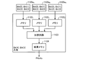
- FIG. 23 is a block diagram showing a configuration of an example of the counter 1120c applicable to the first embodiment.
- the counter 1120c includes a memory 1122 1, 1122 2 and 1122 3, an adder 1123, a result memory 1124, the.
- the memory 1122 1 is supplied with the output of the LSB side counter 1120 a 1 corresponding to the photoelectric conversion element 110 1 .
- the memory 1122 1 stores the output values supplied from the counters 1120a 1 . That is, the memory 1122 1 stores the overflow value in the counter 1120a 1 .
- the memory 1122 1 functions as a counter for counting the bits on the MSB side.
- the memories 1122 2 and 1122 3 also store the overflow values in the LSB side counters 1120a 2 and 1120a 3 corresponding to the photoelectric conversion elements 110 2 and 110 3 , respectively.
- the values stored in the memories 1122 1 , 1122 2 and 1122 3 are added by the adder circuit 1123 and stored in the result memory 1124.
- the value read from the result memory 1124 is output as photon information PhInfo and is supplied to, for example, the threshold value determination unit 113a.
- FIG. 24 is a block diagram showing a configuration of an example of the counter 112h of the eighth example applicable to the first embodiment.
- the counter 112h includes an analog counter 1125a.
- the voltage extracted by the analog counter 1125a is supplied as photon information PhInfo to the threshold value determination unit 113a(d) corresponding to the threshold value determination unit 113a in FIG.
- the threshold value determining unit 113a(d) includes a comparator 1133, and the comparator 1133 compares the photon information PhInfo supplied from the counter 112h with the threshold value Nth supplied as a voltage value.
- the comparator 1133 outputs the write signal WRen(W) when the voltage value of the photon information PhInfo is higher than the voltage value of the threshold value Nth, for example.
- the ninth example is an example in which the pulse Vpls is counted using an analog counter and a digital counter that counts with two values of “0” and “1”.
- FIG. 25 is a block diagram showing a configuration of an example of the counter 112i of the ninth example applicable to the first embodiment.
- the counter 112i includes an analog counter 1125b and a digital counter 112j serially connected to the analog counter 1125b.
- the digital counter 112j any of the counters 112a to 112e described above may be applied.
- the analog counter 1125b applied to the ninth example has a capacitor like the analog counter 1125a described above, and stores an electric charge corresponding to the voltage of the input pulse Vpls in the capacitor.
- the analog counter 1125b according to the ninth example is further configured to monitor the amount of charge accumulated in the capacitor and output a pulse when a predetermined amount or more of charge is accumulated in the capacitor.
- the analog counter 1125b detects the amount of charge stored in the capacitor in predetermined gradations (for example, 16 gradations) and outputs a pulse for each gradation.
- the analog counter 1125b detects one gradation in response to the input of one pulse Vpls.
- the analog counter 1125b resets the counter when the amount of charge accumulated in the capacitor reaches a predetermined gradation.
- the digital counter 112j counts the pulses output from the analog counter 1125b, and outputs the count value as photon information PhInfo.
- the photon information PhInfo is supplied to the threshold value determination unit 113a, for example, when the digital counter 112j corresponds to the counter 112a described above.
- the pulse Vpls are counted by using a digital counter, an analog counter, and a counter composed of a memory and an adder.
- FIG. 26 is a block diagram showing a configuration of an example of the counter 112k of the tenth example applicable to the first embodiment.
- the counter 112k includes a digital counter 1126, an analog counter 1125c serially connected to the digital counter 1126, a memory 1127, and an adder 1128.
- the digital counter 1126 is, for example, a 1-bit counter and can be configured by using one T-FF. Further, it is assumed that the analog counter 1125b described above is applied to the analog counter 1125c.
- the digital counter 1126 outputs a voltage indicating a value "1" in response to the input of the pulse Vpls. This voltage is supplied to the analog counter 1125c and stored in the capacitor.
- the analog counter 1125c detects the amount of charge stored in the capacitor in predetermined gradations (for example, 16 gradations) and outputs a pulse for each gradation.
- the adder 1128 has first and second input terminals, and adds and outputs a signal input to the first input terminal and a signal input to the second input terminal.
- the output of the adder 1128 is input to and stored in the memory 1127.
- the signal read from the memory 1127 is output as photon information PhInfo and is supplied to the second input terminal of the adder 1128.
- the counter can be configured by the adder 1128 and the memory 1127.
- the memory 1127 can be configured by using a capacitor.
- the photon information PhInfo output from the memory 1127 is supplied to the threshold value determination unit 113a (d) corresponding to the threshold value determination unit 113a in FIG.
- the threshold value determination unit 113a (d) for example, the same configuration as the threshold value determination unit 113a (d) described with reference to FIG. 24 can be applied. That is, the threshold value determination unit 113a (d) compares the photon information PhInfo supplied from the counter 112k with the threshold value Nth supplied as a voltage value by the comparator 1133, and writes the write signal WRen (W) according to the comparison result. ) Is output.
- FIG. 27 is a diagram illustrating an arrangement example of the TC generation unit 120 and the pixel circuit 100 according to the first arrangement example according to the first embodiment.
- a TC generation unit 120 is provided for each pixel circuit 100. That is, the vertical control unit 2013a includes a number of TC generation units 120 corresponding to the number of pixel circuits 100 included in the pixel array unit 2001. Each TC generation unit 120 supplies the signal SH_ON and the time code Tc to the corresponding pixel circuit 100, respectively.
- the issuance speed (time interval) of the time code Tc can be controlled for each pixel circuit 100. Therefore, it is possible to suppress variations in each pixel circuit 100.
- FIG. 28 is a diagram showing an arrangement example of the TC generation unit 120 and the pixel circuit 100 according to the second arrangement example according to the first embodiment.
- a TC generation unit 120 is provided for each row of each pixel circuit 100 arranged in a two-dimensional grid pattern in the pixel array unit 2001. .. That is, the second arrangement example according to the first embodiment has a configuration corresponding to FIG. 8 described above.
- the TC generator 120 commonly supplies the time code Tc and the signal SH_ON to each pixel circuit 100 arranged in the corresponding row of the two-dimensional lattice.
- the configuration according to the second arrangement example according to the first embodiment is compatible with the existing sensor. In addition, it is possible to reduce wiring as compared with the configuration according to the first arrangement example according to the first embodiment described above.
- FIG. 29 is a diagram illustrating an arrangement example of the TC generation unit 120 and the pixel circuit 100 according to the third arrangement example according to the first embodiment.
- a TC generation unit 120 is provided in every two rows of each pixel circuit 100 arranged in a two-dimensional grid pattern in the pixel array unit 2001. There is.
- the TC generation unit 120 commonly supplies the time code Tc and the signal SH_ON to each pixel circuit 100 arranged in the corresponding two rows of the two-dimensional lattice.
- FIG. 30 is a diagram showing a third arrangement example according to the first embodiment, paying attention to the pixel array unit 2001.
- each pixel circuit 100 arranged in a two-dimensional lattice in the pixel array section 2001 can handle a group 150 of two rows of a two-dimensional lattice as a unit. That is, the TC generation unit 120 is provided for each group 150, and the time code Tc and the signal SH_ON from the corresponding TC generation unit 120 are supplied to each pixel circuit 100 included in the group 150.
- the configuration according to the third arrangement example according to the first embodiment can reduce the wiring as compared with the configuration according to the second arrangement example according to the first embodiment described above.
- FIG. 31 is a diagram showing an arrangement example of the TC generation unit 120 and the pixel circuit 100 according to the fourth arrangement example according to the first embodiment.
- the TC generation unit 120 is provided for each region in the pixel array unit 2001.
- the time code Tc and the signal SH_ON are commonly supplied from the TC generation unit 120 corresponding to the region to each pixel circuit 100 included in each region.
- one TC generation unit 120 to the time code Tc for the group 150 by each pixel circuit 100 included in the region provided in the pixel array unit 2001.
- the signal SH_ON is also supplied.
- the bias condition of each pixel circuit 100 can be controlled for each region.
- the bias condition of each pixel circuit 100 can be controlled for each region.
- the fifth arrangement example according to the first embodiment is an example in which a color filter is provided in the photoelectric conversion element 110 included in each pixel circuit 100.
- the pixel circuits 100 including the photoelectric conversion elements 110 provided with the color filters of the same color are grouped together, and TC generation is performed for each group.
- a unit 120 is provided.
- FIG. 32 is a diagram showing an arrangement example of the TC generation unit 120 and the pixel circuits 100R, 100G and 100B according to the fifth arrangement example according to the first embodiment.
- the pixel circuits 100R, 100G, and 100B each include a photoelectric conversion element 110 provided with R (red), G (green), and B (blue) color filters.
- the pixel circuits 100R, 100G, and 100B are arranged according to the Bayer array. That is, in each pixel circuit 100R, 100G and 100B, one pixel circuit 100R and 100B and two pixel circuits 100G are arranged in a 2 ⁇ 2 array so that pixel circuits of the same color are not adjacent to each other. Will be done.
- the pixel circuits 100R and 100G are alternately arranged in the first row from the top.
- the time code Tc R1 and the signal SH_ON R1 (not shown) are supplied from the TC generator 120R 1 to the group 150R 1 including each pixel circuit 100R arranged in the first row.
- the time code Tc G11 and the signal SH_ON G11 (not shown) are supplied from the TC generation unit 120G 11 to the group 150G 11 including each pixel circuit 100G arranged in the first line.
- the time code Tc G12 and the signal SH_ON G12 are supplied from the TC generator 120G 12 to the group 150G 12 including each pixel circuit 100G arranged in the second line. Further, the time code Tc B1 and the signal SH_ON B1 (not shown) are supplied from the TC generation unit 120B 1 to the group 150B 1 including each pixel circuit 100B arranged in the second row.
- the TC generator 120R 2 outputs the time code Tc R2. And the signal SH_ON R2 (not shown) is supplied. Further, the time code Tc G21 and the signal SH_ON G21 (not shown) are supplied from the TC generator 120G 21 to the group 150G 21 including each pixel circuit 100G arranged in the third row.
- the time code Tc G22 and the signal SH_ON G22 are supplied from the TC generator 120G 22 to the group 150G 22 including each pixel circuit 100G arranged on the fourth line. Further, the time code Tc B2 and the signal SH_ON B2 (not shown) are supplied from the TC generation unit 120B 2 to the group 150B 2 including each pixel circuit 100B arranged in the fourth line.
- pixel circuits provided with color filters of the same color are grouped into the same group for each of the 5th and 6th rows, the 7th row and the 8th row,...
- the time code Tc and the signal SH_ON are supplied from the common TC generator.
- Each photoelectric conversion element 110 provided with R color, G color and B color color filters has different sensitivity to incident photons.
- the TC generation unit 120 is provided for each of the pixel circuits 100R, 100G, and 100B for each color of the color filter. Therefore, it is possible to correct the different sensitivity of the photoelectric conversion element 110 depending on the color of the color filter by controlling the number of photons prediction based on the predicted count value Npre.
- FIG. 33 is a diagram showing an arrangement example of the TC generation unit 120 and the pixel circuits 100R, 100G 1 , 100G 2 and 100B according to the sixth arrangement example according to the first embodiment.
- the pixel circuits 100G 1 and 100G 2 respectively correspond to the two G pixels included in the Bayer array.
- all the pixel circuits 100R, 100G 1 , 100G 2 and 100B included in the pixel array unit 2001 are included in one group 150RGB.
- a time code Tc RGB and a signal SH_ON RGB (not shown) are commonly supplied by one TC generator 120 RGB to all the pixel circuits 100R, 100G 1 , 100G 2 and 100B included in the group 150 RGB .
- the arrangement of the pixel circuits 100R, 100G and 100B, and the arrangement of the pixel circuits 100R, 100G 1 , 100G 2 and 100B is not limited to the Bayer type. ..
- the color filter provided in the pixel circuit 100 is not limited to the primary color filters of three colors of R, G, and B, and for example, the complementary colors of four colors of C (cyan), M (magenta), Y (yellow), and G. It may be a system filter.
- each pixel circuit 100 may be provided with another type of optical filter.
- an IR filter may be provided for each pixel circuit 100 in order to selectively transmit light in the infrared region.
- each pixel circuit 100 may be provided with a transparent filter that transmits light in a wide wavelength band including the R, G, and B wavelength bands, for example. Also in this case, it is conceivable to provide a transparent filter for one pixel circuit 100 of the pixel circuits 100 provided with the G color filter in the Bayer array, similarly to the above-described IR filter.
- a color filter array different from the Bayer type array there is a 4-split Bayer type RGB array.
- the four-division Bayer RGB array four R color filters, G color filters, and B color filters each having 2 ⁇ 2 photoelectric conversion elements 110 arranged in a one-to-one correspondence are provided in the 2 ⁇ 2 matrix. It is arranged according to the Bayer array in the unit of.
- the array of each pixel circuit 100 provided with the R, G, and B color filters may be used as the 4-split Bayer type RGB array.
- FIG. 34 is a block diagram showing a configuration of an example of the pixel array unit 2001 and the vertical control unit 2013a according to the first modification of the first embodiment.
- the vertical control unit 2013a has the same configuration as the vertical control unit 2013a in FIG. 8 described above, and thus the description thereof will be omitted here.
- the pixel circuit 100b includes a photoelectric conversion element 110, a signal processing unit 111b, a counter 112, a threshold value determination unit 113a-1, and a memory 114, similarly to the pixel circuit 100a shown in FIG. ,including.
- the write signal WRen output from the threshold determination unit 113 is supplied to the memory 114 and the signal processing unit 111b.
- the signal processing unit 111b limits the operation of the photoelectric conversion element 110 when the counted number of photons exceeds the threshold value Nth within the exposure period Tsh and the write signal WRen is in a state of instructing the writing of the time code Tc. ..
- the signal processing unit 111b disconnects the connection to the power potential VDD to the photoelectric conversion element 110 in response to the write signal WRen (W), and at the start of the exposure period Tsh, the power potential VDD to the photoelectric conversion element 110 is reached. It is possible to restore the connection of the.
- the power consumption in the pixel circuit 100b can be reduced.
- FIG. 35 is a block diagram showing a configuration of an example of the pixel array unit 2001 and the vertical control unit 2013a according to the second modification of the first embodiment.
- the vertical control unit 2013a has the same configuration as the vertical control unit 2013a in FIG. 8 described above, and thus the description thereof will be omitted here. Further, in the pixel array section 2001, the functions of the signal processing section 111b' and the threshold value determining section 113a-2 of the pixel circuit 100c are changed as compared with the pixel circuit 100b of FIG.
- the threshold value determination unit 113a-2 in response to the detection of the threshold value Nth by the threshold value determination unit 113a-2, the photoelectric conversion element 110 Limit operation.
- the threshold value determination unit 113a-2 in response to the detection of the threshold value Nth by the threshold value determination unit 113a-2, the photoelectric conversion element 110 Limit operation.
- the threshold value determination unit 113a-2 according to the second modification of the first embodiment generates and generates a signal PhGating for limiting the operation of the photoelectric conversion element 110, separately from the write signal WRen.
- the signal PhGating is supplied to the signal processing unit 111b′.
- the signal processing unit 111b' limits the operation of the photoelectric conversion element 110 according to the signal PhGating. For example, the signal processing unit 111b′ disconnects the connection to the power supply potential VDD with respect to the photoelectric conversion element 110 according to the signal PhGating, and connects the connection to the power supply potential VDD with respect to the photoelectric conversion element 110 at the start of the exposure period Tsh. It is possible to recover.
- the power consumption in the pixel circuit 100c can be reduced.
- a dual mode counter capable of switching between a count operation and a storage operation is used as a counter for counting the pulses Vpls corresponding to the incidence of photons on the photoelectric conversion element 110.
- the dual mode counter for example, the memory 114 in the pixel circuit 100a shown in FIG. 8 can be omitted, and the circuit area can be reduced.
- FIG. 36 is a block diagram showing the configuration of an example of a pixel array unit 2001 and a vertical control unit 2013a according to a third modification of the first embodiment.
- the vertical control unit 2013a has the same configuration as the vertical control unit 2013a in FIG. 8 described above, and a description thereof will be omitted here.
- the pixel circuit 100d has a different function of the threshold value determination unit 113a-3 as compared with the pixel circuit 100a of FIG. 8, the memory 114 is omitted, and the dual circuit 100d is replaced with the counter 112.
- a mode counter 115 is provided.
- pulses Vpls corresponding to the incident of photons on the photoelectric conversion element 110 are input to the dual mode counter 115. Further, the time code Tc output from the TC generator 120 is input to the dual mode counter 115.
- the dual mode counter 115 has a count operation mode and a storage operation mode as operation modes. Further, the storage operation mode includes a writing operation mode and a holding operation mode. The dual mode counter 115 switches these operation modes according to the signal WRen_CNT supplied from the threshold value determination unit 113 ”. The dual mode counter 115 counts the operation mode when the signal WRen_CNT indicates a count operation. The operation mode is switched, the pulse Vpls supplied from the signal processing unit 111a is counted, and the photon information PhInfo indicating the count result is output. Further, the dual mode counter 115 indicates that the signal WRen_CNT indicates a storage operation. The operation mode is switched to the storage operation mode and the input time code Tc is stored.
- the threshold value determination unit 113a-3 outputs a signal WRen_CNT indicating a counting operation at the start of the exposure period Tsh.
- the operation mode of the dual mode counter 115 is switched to the count operation mode.
- the dual mode counter 115 counts the pulse Vpls supplied from the signal processing unit 111a and outputs the count result as photon information PhInfo.
- the threshold value determination unit 113a-3 stores, for example, when it is determined that the number of photons incident on the photoelectric conversion element 110 within the exposure period Tsh has reached the threshold value Nth.
- a signal WRen_CNT indicating the operation is output.
- the dual mode counter 115 switches the operation mode to the storage operation mode according to this signal WRen_CNT, stops counting the pulse Vpls, and stores the time code Tc.
- FIG. 37A to 37C are diagrams for explaining the operation of the dual mode counter 115 applicable to the third modification of the first embodiment.
- FIG. 37A is a diagram showing a state of the dual mode counter 115 in the count operation mode.
- FIG. 37B is a diagram showing a state of the dual mode counter 115 in the write operation mode in the storage operation mode.
- FIG. 37C is a diagram showing a state of the dual mode counter 115 in the holding operation mode in the storage operation mode.
- the dual mode counter 115 is a 5-bit counter.
- the dual mode counter 115 applicable to the third modification of the first embodiment has five D-FFs (D flip-flops) 1140 0 , 1140 1 , 1140 2 , 1140 3 corresponding to the number of bits to be counted. And 1140 4 .
- D-FFs D flip-flops
- D-FF1140 0 is, terminal D and terminal QB, is connected via a switch 1142 0 controlled in accordance with signals WRen_CNT.
- the terminal QB indicates a terminal with an overline on "Q" in the figure.
- the terminal D and the terminal QB pass through the switches 1142 1 , 1142 2 , 1142 3 and 1142 4 respectively controlled according to the signal WRen_CNT. Is connected.
- the common selection end of the switch 1143 0 controlled according to the signal WRen_CNT is connected to the terminal CK of the D-FF 1140 0 .
- the pulse Vpls is input to the first selection end of the switch 1143 0 , and the low-level potential and the high-level potential are connected to the second and third selection ends, respectively.
- the terminals QB of the preceding stage are connected to the first selection terminals of the respective terminals CK, and the second and third selection terminals of the low level respectively.
- the common selective ends of switches 1143 1 , 1143 2 , 1143 3 and 1143 4 controlled according to the signal WRen_CNT, to which the potential and the high level potential are connected, are connected.
- each of the D-FFs 1140 0 , 1140 1 , 1140 2 , 1140 3 and 1140 4 outputs the respective bits (Bit(0), Bit(1), Bit(2), Bit(3) and Bit(3)) from the output terminal Q. (4)) is output.
- the photon information PhInfo is output from the output terminal QB of the D-FF 1140 4 in the final stage.
- Each D-FF1140 0 ⁇ 1140 4, the switches 1141 0-1141 4, the switches 1142 0-1142 4, and, the switches 1143 0-1143 4 is controlled in the same state, respectively, in each of the operation modes .. Therefore, in the following, unless otherwise stated, we perform a D-FF1140 0, the description of the D-FF1140 0 switch 1141 connected to the 0, 1142 0 and 1143 0 as an example.
- switch 1141 0 off (open) state
- the switch 1142 0 is controlled to be turned on (closed) state
- the switch 1143 0 common It is controlled to connect the selection end to the first selection end.
- D-FF1140 0 together with output and terminal QB and the terminal D are connected, a pulse Vpls the terminal CK is input from the output terminal Q and QB, inverted every falling edge of the input pulse Vpls The output is retrieved.
- Output terminal QB of the D-FF1140 0 is input to the next-stage D-FF1140 1 terminal CK.
- the D-FF 1140 1 takes out from the output terminals Q and QB an output that is inverted every time the output of the terminal QB of the D-FF 1140 0 falls.
- the dual mode counter 115 operates as a counter that counts the pulse Vpls in the count operation mode.
- the switch 1141 0 is controlled to be in the on state and the switch 1142 0 is controlled to be in the off state, and the switch 1143 0 is set as the common selection end to the third selection end. Controlled to connect to.
- a predetermined bit of the time code Tc is input to the terminal D of the D-FF 1140 0 via the switch 11410, the terminal CK is set to the high state, and the terminal D of the D-FF 1140 0 is supplied with the time code Tc. The value of a predetermined bit is written.
- the operation of the dual mode counter 115 is shifted to the holding operation mode, as shown in FIG. 37C, the switches 1141 0 and 1142 0 are controlled to the off state, and the switch 1143 0 causes the common selection end to become the second selection end. Controlled to connect to.
- the terminal CK is set to the low state, and the value written in the terminal D is held in the D-FF 1140 0 .
- the retention mode it is possible from the output terminal Q each of D-FF1140 0 ⁇ 1140 4, taking out the D-FF1140 0 ⁇ written in 1140 fourth terminal D held value.
- the predicted count value Npre predicted based on the time Tth at which the count value reaches the threshold value Nth is a 15-bit value and the threshold value Nth is a 9-bit value.
- the significant figure of the predicted count value Npre is a 9-bit value. That is, of the 15 bits of the predicted count value Npre, 6 bits are invalid numbers. Further, in this case, the bit on the LSB side of the predicted count value Npre is considered to have low importance. Therefore, the number of bits of the predictive count value Npre can be reduced by ignoring the 15-bit value of the predictive count value Npre by ignoring the predetermined bits on the LSB side.
- the 15-bit predicted count value Npre is represented by an 8-bit significant figure and a 3-bit shift amount.
- the value "20480” in decimal notation is the 15-bit value "0b101000000000000000” in binary notation.
- the 3-bit shift amount “0b111” is applied to this 15-bit value, the following expression (5) is obtained.
- 0b101000000000000 0b101000000 ⁇ 2 ⁇ (0b111)... (5)
- the 15-bit predicted count value Npre can be expressed as, for example, an 11-bit value "0b111100000” by using an 8-bit value "0b1010000” and a 3-bit shift amount "0b111".
- the first 3 bits indicate the shift amount. In this way, the number of bits of the predicted count value Npre can be reduced from 15 bits to 11 bits.
- the signal processing unit 2013c applies the above equation (5) when, for example, calculating the predicted count value Npre based on the time code Tc read from the memory 114 of each pixel circuit 100a. Then, the number of bits of the calculated predicted count value Npre is reduced. As a result, for example, it is possible to reduce the processing and memory capacity in the signal processing unit 2013c and the traffic when outputting the calculated predicted count value Npre to the outside.
- the correlation prediction count value Npre_related can also be calculated based on the prediction count value Npre_reduce with a reduced number of bits described using the equations (4) and (5).
- Npre_related Npre_reduce + Noffset ... (7)
- the signal processing unit 2013c is calculated by applying the above equation (6) when calculating the predicted count value Npre based on, for example, the time code Tc read from the memory 114 of each pixel circuit 100a.
- the correlation predicted count value Npre_related corresponding to the predicted count value Npre is calculated. Thereby, for example, it is possible to reduce the load of the processing in the signal processing unit 2013c and the processing for the predicted count value Npre outside.
- the conversion process for the predicted count value Npre is described as a process of adding an offset value, but this is not limited to this example. That is, for example, in the signal processing unit 2013c, it is possible to perform various conversion processes on the predicted count value Npre depending on its use and the like.
- This conversion processing can also include processing for converting the data format, such as Gray code.
- FIG. 38 is a diagram showing a schematic configuration example of the light receiving device according to the second embodiment.
- the light receiving device 1b according to the second embodiment includes a pixel 10, a counting unit 11, a luminance value code generation unit 20, and an acquisition unit 13.
- the pixel 10 includes a photoelectric conversion element that converts light into an electric charge by photoelectric conversion, and a signal processing circuit that reads an electric charge from the photoelectric conversion element and outputs it as an electric signal.
- the SPAD can be applied as in the first embodiment described above.
- the light receiving device 1b predicts the brightness value according to the number of photons incident on the pixel 10 within the designated exposure period Tsh, and the brightness generated by the brightness value code generation unit 20 corresponding to the predicted brightness value.
- the value code Lc is acquired by the acquisition unit 13.
- the counting unit 11 counts the pulse Vpls output from the pixel 10 within the specified exposure period Tsh, and when the number Ncnt of the counted pulse Vpls exceeds the threshold value Nth before the end of the exposure period Tsh. ,
- the write signal WRen (W) is output.
- the write signal WRen is supplied to the acquisition unit 13.
- the brightness value code generation unit 20 predicts the brightness value at the end time of the exposure period Tsh according to the elapsed time from the start time of the exposure period Tsh to the time when writing is instructed by the write signal WRen(W). Then, a luminance value code Lc indicating the predicted luminance value is generated. The luminance value code Lc generated by the luminance value code generation unit 20 is supplied to the acquisition unit 13.
- the acquisition unit 13 includes a memory, for example, and is supplied from the brightness value code generation unit 20 at the timing when writing is instructed by the write signal WRen(W), that is, at the timing when the write signal WRen changes from the low state to the high state.
- the obtained luminance value code Lc is acquired, and the acquired luminance value code Lc is written to the memory.
- the light receiving device 1b according to the second embodiment is the light receiving chip 2000 made of a semiconductor chip and the logic chip 2010, which are described with reference to FIG. 5, in the same manner as the light receiving device 1a according to the first embodiment described above. A structure in which and is laminated can be applied.
- the brightness (luminance value) for a certain pixel (photoelectric conversion element 110) and the average photon arrival interval Ta, which is the average incident interval of photons incident on the pixel, are in an inversely proportional relationship.
- Lx (T ⁇ k) / Ta... (8)
- Tth ev Nth ⁇ Ta (9)
- the luminance value Lx in the equation (10) is a value expected when the number of photons Pn incident on the photoelectric conversion element 110 reaches the threshold value Nth, and is a prediction predicted at the threshold value Nth.
- the brightness value is Lpre.
- FIG. 39 is a diagram showing an example relationship between the time Tth at which the number of photons Pn reaches the threshold value Nth and the predicted luminance value Lpre according to the second embodiment.
- the luminance value Lx in the above equation (10) is shown as the predicted luminance value Lpre.
- the expected time Tth ev the time Tth when the number Pn of photons incident on the photoelectric conversion element 110 reaches the threshold value Nth can be used.
- the predicted brightness value Lpre in the exposure period Tsh can be obtained by referring to the curve LT according to Expression (10) based on the time Tth 0 .
- the threshold value Nth, the time T (exposure period Tsh), and the coefficient k are constants given in advance.
- the luminance value code generation unit 20 can store the curve LT in advance as a table in which the predicted luminance value Lpre and the time Tth are associated with each other.
- the table stores the predicted luminance value Lpre as a discrete value, the luminance value code Lc, in association with the corresponding time Tth.
- the brightness value code generation unit 20 may calculate the predicted brightness value Lpre using the threshold value Nth, the time T (exposure period Tsh) and the coefficient k based on the measured time Tth. Also in this case, the calculated predicted luminance value Lpre is processed into discrete values and used as the luminance value code Lc.
- FIG. 40 is a diagram for schematically explaining the generation of the predicted luminance value Lpre by the luminance value code generation unit 20 according to the second embodiment.
- FIG. 40 from the top, the passage of time, an example of the count value in the case of low illuminance, an example of the count value in the case of high illuminance, an example of evenly spaced time codes Tc, and an example of the predicted brightness value Lpre are shown. Each is shown.
- the passage of time an example of the count value in the case of low illuminance, an example of the count value in the case of high illuminance, and an example of the time code Tc at equal intervals are the same as the corresponding parts in FIG. 3 described above. Therefore, the description here will be omitted.
- the time scale is longer than that in FIG.
- the predicted luminance value Lpre is shown with the passage of time. It schematically shows how it decreases in inverse proportion to the time Tth. More specifically, in the example of FIG. 40, the predicted luminance value Lpre has values of "22", “17”, “14”, ... At short intervals on the side close to the start time t 0 of the exposure period Tsh. , The value decreases rapidly. On the other hand, near the end of the exposure period Tsh, the change in the predicted luminance value Lpre with time becomes small, and the change interval also becomes long.
- the timing at which the eighth photon Ph (28) is detected is the time Tth when the count value exceeds the threshold value Nth.
- the value “11” of the time code Tc corresponding to this time Tth is set.
- the predicted brightness value Lpre has a value of "10".
- the predicted luminance value Lpre increases rapidly as the time Tth approaches 0, and becomes infinite when the time Tth is 0. Therefore, in the period when the time Tth is extremely short, the predicted luminance value Lpre becomes an extremely large value, and the predicted luminance value Lpre within the period becomes a value that does not make sense in reality. This means that the predicted luminance value Lpre in the period is unnecessary. Therefore, for example, in the table in which the predicted luminance value Lpre and the time Tth are associated with each other, the time Tth is targeted only for the time after the predetermined time has elapsed from the start time of the exposure period Tsh, and the predicted brightness before that time The value Lpre can not be defined in the table.
- the predicted brightness value Lpre predicted in the exposure period Tsh is directly obtained based on the time Tth when the number Pn of photons incident on the photoelectric conversion element 110 reaches the threshold Nth. Can be done.
- the light receiving device 1b according to the second embodiment can reduce the load of the process of converting the time code Tc into the luminance value as compared with the light receiving device 1a according to the first embodiment. ..
- the signal processing unit 2013c reads each time code from each logic circuit 2014 included in the logic array unit 2011 (see FIG. 7). A process of converting each Tc into a brightness value is executed. That is, in the light receiving device 1a according to the first embodiment, the signal processing unit 2013c converts, for example, at least each time code Tc read from the logic circuit 2014 for one row included in the logic array unit 2011 into a brightness value. It is necessary to end the processing to be performed within one horizontal synchronization period.
- each of the logic circuits 2014 included in the logic array unit 2011, a process of converting the time Tth when the number of incident photons reaches the threshold Nth into a brightness value is performed. Running. Since the conversion process of the time information into the luminance value is distributed and executed in each logic circuit 2014, each conversion process can be small and the processing in the signal processing unit 2013c can be reduced.
- FIG. 41 is a block diagram showing an example configuration of the pixel array unit 2001 and the vertical control unit 2013a according to the second embodiment. Further, in FIG. 41, a more specific configuration of the pixel circuit is shown with respect to the pixel array unit 2001. In FIG. 41, the same reference numerals are given to the parts common to those in FIG. 8 described above, and detailed description thereof will be omitted.
- the pixel array unit 2001 has a configuration corresponding to the pixel array unit 2001 described with reference to FIG. 8, and a plurality of pixel circuits 100a'corresponding to the pixel circuit 100a of FIG. 8 respectively. including. Note that, in FIG. 41, among the pixel circuits 100 a ′ arranged in a two-dimensional lattice pattern in the pixel array section 2001, the pixel circuits 100 a ′ included in one row are extracted and shown.
- the pixel circuit 100a' includes a photoelectric conversion element 110, a signal processing unit 111a, a counter 112, a threshold value determination unit 113b, and a memory 114.
- the photoelectric conversion element 110, the signal processing unit 111a, the counter 112, and the threshold value determination unit 113b have the same functions as the photoelectric conversion element 110, the signal processing unit 111a, the counter 112, and the threshold value determination unit 113a in FIG. , The description here is omitted.
- SPAD can be applied in the same manner as in the first embodiment described above.
- the memory 114 stores the luminance value code Lc as the predicted luminance value Lpre supplied from the LC generation unit 200, which will be described later, in response to the write signal WRen (W) supplied from the threshold value determination unit 113b.
- the vertical control unit 2013a' corresponds to the vertical control unit 2013a in FIG. 8 and includes an LC (luminance value code) generation unit 200 for each row.
- a timer 210 is included in common to each line.
- the LC generation unit 200 corresponds to the above-mentioned luminance value code generation unit 20.
- the LC generation unit 200 has a luminance value that changes in inverse proportion to the elapsed time from the start time of the exposure period Tsh, which has been described with reference to FIGS. 39 and 40, based on, for example, the time information supplied from the timer 210. Generate code Lc.
- the timer 210 generates, for example, based on a clock signal, for each change in the predicted luminance value Lpre described with reference to FIG. 40, time information indicating the timing of the change.
- FIG. 42 is a block diagram showing a configuration of an example of the LC generation unit 200 applicable to the second embodiment.
- the luminance value code Lc is stored as a table associated with the time Tth.
- the LC generation unit 200 includes a ROM (Read Only Memory) 201 and a code generation control unit 202.
- the ROM 201 stores in advance a table in which the luminance value code Lc and the time Tth are associated with each other.
- the code generation control unit 202 reads the luminance value code Lc corresponding to the time information supplied from the outside, for example, the timer 210, from the ROM 201.
- the luminance value code Lc read from the ROM 201 by the code generation control unit 202 is input to each pixel circuit 100a′, 100a′,... Included in the pixel array unit 2001 and supplied to each memory 114. Will be done.
- control unit 1003 instructs the LC generation unit 200 to start the exposure period Tsh, and supplies information indicating the length of the exposure period Tsh to the LC generation unit 200.
- the LC generation unit 200 generates a signal SH_ON instructing the timing at which the signal processing unit 111a outputs the pulse Vpls.
- the LC generation unit 200 generates the signal SH_ON based on, for example, a predetermined clock signal.
- the signal SH_ON generated by the LC generation unit 200 is input to the pixel circuits 100a', 100a', ..., And is supplied to the signal processing unit 111a.
- the counters 112a to 112i and the digital counters 112j described with reference to FIGS. 16A and 16B, FIGS. 17, 18, 19A and 19B, and FIGS. 20 to 26 are similar to the pixel circuit 100a described above. It is also applicable to the pixel circuit 100a'according to the second embodiment.
- FIG. 43 is a diagram showing an arrangement example of the LC generation unit 200 and the pixel circuit 100 ′ according to the first arrangement example according to the second embodiment.
- the first arrangement example according to the second embodiment corresponds to the first arrangement example according to the first embodiment described with reference to FIG. 27, and as shown in FIG. 43, the LC generation unit 200 Is provided for each pixel circuit 100'. That is, the vertical control unit 2013a'includes a number of LC generation units 200 corresponding to the number of pixel circuits 100' included in the pixel array unit 2001. Each LC generation unit 200 supplies the signal SH_ON and the luminance value code Lc to the corresponding pixel circuit 100', respectively.
- the issuing speed (time interval) of the luminance value code Lc can be controlled for each pixel circuit 100'. Therefore, it is possible to suppress the variation between the pixel circuits 100'.
- FIG. 44 is a diagram showing an arrangement example of the LC generation unit 200 and the pixel circuit 100 ′ according to the second arrangement example according to the second embodiment.
- the second arrangement example according to the second embodiment corresponds to the second arrangement example according to the first embodiment described with reference to FIG. 28, and as shown in FIG. 44, the vertical control unit 2013a
- the pixel array unit 2001 is provided with an LC generation unit 200 for each row of each pixel circuit 100'arranged in a two-dimensional grid. That is, the second arrangement example according to the second embodiment is The LC generation unit 200 supplies the brightness value code Lc and the signal SH_ON in common to each pixel circuit 100'arranged in the corresponding rows of the two-dimensional lattice. ..
- the configuration according to the second arrangement example according to the second embodiment is compatible with the existing sensor. In addition, it is possible to reduce the wiring as compared with the configuration according to the first arrangement example according to the second embodiment described above.
- FIG. 45 is a diagram showing an arrangement example of the LC generation unit 200 and the pixel circuit 100 ′ according to the third arrangement example according to the second embodiment.
- the third arrangement example according to the second embodiment corresponds to the third arrangement example according to the first embodiment described with reference to FIG. 29, and as shown in FIG. 45, the pixel array unit 2001
- An LC generation unit 200 is provided for every two rows of each pixel circuit 100'arranged in a two-dimensional lattice.
- the LC generation unit 200 commonly supplies the luminance value code Lc and the signal SH_ON to each pixel circuit 100'arranged in the corresponding two rows of the two-dimensional lattice.
- the configuration according to the third arrangement example according to the second embodiment can reduce the wiring as compared with the configuration according to the second arrangement example according to the second embodiment described above.
- FIG. 46 is a diagram illustrating an arrangement example of the LC generation unit 200 and the pixel circuit 100′ according to the fourth arrangement example according to the second embodiment.
- the fourth arrangement example according to the second embodiment corresponds to the fourth arrangement example according to the first embodiment described with reference to FIG. 31, and as shown in FIG. 46, the pixel array unit 2001
- a luminance value code Lc and a signal SH_ON (not shown) are commonly supplied to each pixel circuit 100 ′ included in each area from the LC generation unit 200 corresponding to the area.
- the brightness from one LC generation unit 200 is relative to the group 150'by each pixel circuit 100'included in the region provided in the pixel array unit 2001.
- the value code Lc and the signal SH_ON are supplied.
- the bias condition of each pixel circuit 100' can be controlled for each region.
- the fifth arrangement example according to the second embodiment corresponds to the fifth arrangement example according to the first embodiment described with reference to FIG. 32, and is a photoelectric conversion included in each pixel circuit 100'. This is an example of the case where the element 110 is provided with a color filter.
- the pixel circuit 100' including the photoelectric conversion element 110 provided with the color filter of the same color is collectively grouped, and each group is LC.
- a generation unit 200 is provided.
- FIG. 47 shows a photoelectric conversion provided with an LC generation unit 200 and R (red), G (green), and B (blue) color filters, respectively, according to a fifth arrangement example according to the second embodiment. It is a figure which shows the arrangement example of the pixel circuit 100R', 100G' and 100B' including the element 110.
- a luminance value code Lc R1 and a signal SH_ON R1 are supplied from the LC generation unit 200R 1 to a group 150R 1 ′ including each pixel circuit 100R′ arranged in the first row from the top. Be supplied. Further, the luminance value code Lc G11 and the signal SH_ON G11 (not shown) are supplied from the LC generation unit 200G 11 to the group 150G 11 ′ including the pixel circuits 100G′ arranged in the first row.
- the luminance value from the LC generator 200G 12 code Lc G12 and signal SH_ON G12 (not shown) is supplied. Further, the luminance value code Lc B1 and the signal SH_ON B1 (not shown) are supplied from the LC generation unit 200B 1 to the group 150B 1 ′ including the pixel circuits 100B′ arranged in the second row.
- the luminance value from the LC generator 200R 2 Code Lc R2 and signal SH_ON R2 are supplied. Further, the luminance value code Lc G21 and the signal SH_ON G21 (not shown) are supplied from the LC generation unit 200G 21 to the group 150G 21 ′ including the pixel circuits 100G′ arranged in the third row.
- the luminance from the LC generator 200G 22 value code Lc G22 and signal SH_ON G22 (not shown) is supplied. Further, the luminance value code Lc B2 and the signal SH_ON B2 (not shown) are supplied from the LC generation unit 200B 2 to the group 150B 2 ′ including the pixel circuits 100B′ arranged in the fourth row.
- the pixel circuits provided with the same color filter for each of the 5th and 6th lines, the 7th line, the 8th line, and so on are grouped in the same group.
- the luminance value code Lc and the signal SH_ON are supplied from the common TC generation unit.
- Each photoelectric conversion element 110 provided with R color, G color and B color color filters has different sensitivity to incident photons.
- the LC generation unit 200 is provided for each of the pixel circuits 100R', 100G', and 100B' collectively for each color of the color filter. Therefore, the sensitivity of the photoelectric conversion element 110, which differs depending on the color of the color filter, is corrected by controlling the predicted luminance value Lpre based on the time Tth for achieving the threshold value Nth (for example, adjusting the table value stored in the ROM 201). Is possible.
- each of the pixel circuits 100R', 100G' and 100B respectively like the 6th and 7th arrangement examples of the 1st Embodiment described above.
- each of the pixel circuits 100R', the arrangement of 100G 1 ', 100G 2' and 100B ' is not limited to Bayer.
- the color filter provided in the pixel circuit 100' is not limited to the primary color filter using the three colors of R, G, and B, and is, for example, the four colors of C (cyan), M (magenta), Y (yellow), and G. It may be a complementary color filter.
- each pixel circuit 100 may be provided with other types of optical filters such as IR filters and transparent filters.
- other types of optical filters such as IR filters and transparent filters may be provided for each pixel circuit 100.
- the array of each pixel circuit 100'provided with R, G, and B color filters may be the above-mentioned 4-split Bayer type RGB array.
- the sixth arrangement example according to the second embodiment corresponds to the sixth arrangement example according to the first embodiment described with reference to FIG. 33, and is a photoelectric conversion included in each pixel circuit 100'.
- FIG. 48 LC generator 200 according to the sixth arrangement example of according to the second embodiment, as well, the pixel circuits 100R ', 100G 1', is a diagram illustrating an arrangement example of 100G 2 'and 100B'.
- all the pixel circuits 100R′, 100G 1 ′, 100G 2 ′ and 100B′ included in the pixel array unit 2001 are included in one group 150RGB′.
- All the pixel circuits 100R in the group 150RGB respect ', 100G 1', 100G 2 ' and 100B', with one LC generator 200RGB, (not shown) luminance value code Lc RGB and signal SH_ON RGB is common Is supplied.
- FIG. 49 is a block diagram showing a configuration of an example of the pixel array unit 2001 and the vertical control unit 2013a ′ according to the first modification of the second embodiment.
- the vertical control unit 2013a' has the same configuration as the vertical control unit 2013a in FIG. 41 described above, and therefore the description thereof is omitted here.
- the pixel circuit 100b′ corresponds to the pixel circuit 100b according to the first modification of the first embodiment described with reference to FIG. 34, and includes the photoelectric conversion element 110 and the signal processing unit. 111b, the counter 112, the threshold value determination part 113b-1, and the memory 114 are included.
- the write signal WRen (W) output from the threshold value determination unit 113b-1 is supplied to the memory 114 and the signal processing unit 111b.
- the signal processing unit 111b limits the operation of the photoelectric conversion element 110 when the counted number of photons exceeds the threshold value Nth within the exposure period Tsh and the write signal WRen is in a state of instructing the writing of the luminance value code Lc. To do. Since the same method as that of the first modification of the first embodiment described above can be applied to limit the operation of the photoelectric conversion element 110, description thereof will be omitted here.
- FIG. 50 is a block diagram showing a configuration of an example of the pixel array unit 2001 and the vertical control unit 2013a ′ according to the second modification of the second embodiment.
- the vertical control unit 2013a' has the same configuration as the vertical control unit 2013a' in FIG. 41 described above, and therefore the description thereof is omitted here. Further, in the pixel array section 2001, the functions of the signal processing section 111b' and the threshold value determining section 113b-2 of the pixel circuit 100c' are changed as compared with the pixel circuit 100b'' of FIG.
- the second modification of the second embodiment corresponds to the pixel circuit 100c according to the second modification of the first embodiment described with reference to FIG. 35, and the threshold value by the threshold value determination unit 113b-2.
- the operation of the photoelectric conversion element 110 is limited according to the detection of Nth.
- the same method as that of the second modification of the first embodiment described above can be applied to limit the operation of the photoelectric conversion element 110, and thus the description thereof is omitted here.
- the third modification of the second embodiment corresponds to the pixel circuit 100d according to the third modification of the first embodiment described with reference to FIG. 36, and the incident of photons on the photoelectric conversion element 110.
- a dual mode counter as a counter for counting the pulses Vpls according to the above, for example, the memory 114 in the pixel circuit 100a shown in FIG. 41 can be omitted, and the circuit area can be reduced.
- FIG. 51 is a block diagram showing the configuration of an example of a pixel array section 2001 and a vertical control section 2013a' according to a third modification of the second embodiment.
- the vertical control unit 2013a' has the same configuration as the vertical control unit 2013a' in FIG. 41 described above, and therefore description thereof will be omitted here.
- the pixel circuit 100d' has changed the function of the threshold value determination unit 113b-3 as compared with the pixel circuit 100a of FIG. 41, the memory 114 is omitted, and the counter 112 is replaced.
- a dual mode counter 115 is provided.
- pulses Vpls corresponding to the incident of photons on the photoelectric conversion element 110 are input to the dual mode counter 115. Further, the luminance value code Lc output from the TC generation unit 120 is input to the dual mode counter 115. Since the configuration and operation of the dual mode counter 115 are the same as the configuration and operation of the dual mode counter 115 described with reference to FIGS. 37A to 37C, the description thereof will be omitted here.
- the dual mode counter 115 switches the operation mode between the count operation mode and the storage operation mode according to the signal WRen_CNT supplied from the threshold value determination unit 113b-3.
- the storage operation mode includes a writing operation mode and a holding operation mode.
- the dual mode counter 115 switches the operation mode to the count operation mode, counts the pulses Vpls supplied from the signal processing unit 111a', and displays the photon information PhInfo indicating the count result. Output.
- the dual mode counter 115 switches the operation mode to the storage operation mode and stores the input luminance value code Lc.
- the compression processing for the predicted count value Npre described using the equations (5) and (6) and the conversion processing for converting the predicted count value Npre into the correlation value described using the equation (7) It is also applicable to this second embodiment and each modification.
- the predicted count value Npre in the equations (5), (6) and (7) is read as the predicted luminance value Lpre.
- the update cycle of the predicted luminance value Lpre is variable. That is, in the example of FIG. 40, the update cycle is shortened on the side close to the start time t 0 of the exposure period Tsh, and the update cycle is lengthened as time elapses from the start time t 0 .
- the update cycle of the predicted brightness value Lpre is fixed.
- FIG. 52 is a diagram for schematically explaining the generation of the predicted luminance value Lpre by the luminance value code generation unit 20 according to the fourth modification of the second embodiment.
- the passage of time an example of the count value in the case of low illuminance, an example of the count value in the case of high illuminance, an example of evenly-spaced time codes Tc, and an example of the predicted luminance value Lpre are shown from the top in FIG. Each is shown.
- the passage of time an example of the count value in the case of low illuminance, an example of the count value in the case of high illuminance, and an example of the time code Tc at equal intervals are the same as the corresponding parts in FIG. 40 described above. Therefore, the description here will be omitted.
- the predicted luminance value Lpre is obtained based on the number of photons incident on the photoelectric conversion element 110, and the update cycle for acquiring the predicted luminance value Lpre is variable. Further, the change of the luminance value code Lc indicating the acquired predicted luminance value Lpre is also variable.
- FIG. 53 is a diagram showing a schematic configuration example of the light receiving device according to the third embodiment.
- the light receiving device 1c according to the third embodiment includes a pixel 10, a counting unit 11, a brightness value code generating unit 20', and an acquiring unit 13.
- the pixel 10 includes a photoelectric conversion element that converts light into an electric charge by photoelectric conversion, and a signal processing circuit that reads the electric charge from the photoelectric conversion element and outputs the electric signal.
- the light receiving device 1c predicts a brightness value according to the number of photons incident on the pixel 10 within the specified exposure period Tsh, and is generated by the brightness value code generation unit 20′ corresponding to the predicted brightness value.
- the brightness value code Lc is acquired by the acquisition unit 13.
- the predicted brightness value Lpre changes in inverse proportion to the time Tth at which the number Pn of photons reaches the threshold value Nth (see FIG. 39).
- the amount of change in the predicted luminance value Lpre per unit time becomes smaller as the time elapses from the start time of the exposure period Tsh.
- the unit time indicates the resolution with respect to time
- the amount of change in the predicted luminance value Lpre per unit time indicates the resolution of the predicted luminance value Lpre.
- FIG. 54 is a diagram showing an example relationship between the resolution of the predicted luminance value Lpre (luminance value resolution) and the time resolution (time resolution) applicable to the third embodiment. From FIG. 54, it can be seen that when the time resolution is constant, the luminance value resolution decreases with the passage of time from the start time of the exposure period Tsh. In other words, when the luminance value resolution is constant, the time resolution becomes lower as time elapses from the start time of the exposure period Tsh. For example, the time resolution may be lower than the time resolution near the start time of the exposure period Tsh as the time elapses from the start time.
- the time interval at which the brightness value code generation unit 20' generates the brightness value code Lc is changed according to the passage of time from the start time of the exposure period Tsh.
- the light receiving device 1c controls the change of the luminance value code Lc generated by the luminance value code generation unit 20'according to the passage of time from the start time of the exposure period Tsh.
- FIG. 55 is a diagram for explaining the generation of the luminance value code Lc in the case of high illuminance and medium illuminance according to the third embodiment.
- the elapsed time, an example of the count value in the case of medium illuminance, an example of the count value in the case of high illuminance, a time value, and an example of the brightness value code Lc are shown from the top.
- the time value is a value that is incremented at predetermined time intervals, and is supplied from, for example, a timer.
- the luminance value code Lc is generated by the luminance code generation unit 20'at intervals according to different update cycles by classifying the illuminance into three stages of, for example, high illuminance, medium illuminance and low illuminance.
- a high illuminance period, a medium illuminance period, and a low illuminance period are assigned to the exposure period Tsh.
- the period of high illuminance is from the start time of the exposure period Tsh to a predetermined time
- the period from the predetermined time to another predetermined time is the period of medium illuminance.
- the period from the other predetermined period to the end of the exposure period Tsh is defined as the low illuminance period.
- the luminance value code generation unit 20 ′ generates the luminance value code Lc at intervals according to the highest update cycle for the period of high illuminance among the periods of high illuminance, medium illuminance, and low illuminance. Further, the luminance value code generation unit 20'generates the luminance value code Lc with discontinuous values during the period of high illuminance. For example, the luminance value code generation unit 20'generates the luminance code Lc whose value is gradually reduced from the position closest to the start time of the exposure period Tsh to the position farthest from the start point of the exposure period Tsh in the high illuminance period (FIG. In the example of 55, the values are "28", "22", "17", "13").
- the predicted luminance value Lpre becomes an extremely large value in a period in which the time Tth is extremely short, and the predicted luminance value Lpre in the period is realistic. Is a value that does not make sense. This means that the luminance value code Lc in the period is unnecessary. Therefore, for example, the brightness value code generation unit 20′ sets the brightness value code Lc having the largest value at the time when a predetermined time has elapsed from the start time of the period in the period of high illuminance, and the period before the time is set. In, the luminance value code Lc may not be set. In the example of FIG.
- the value code Lc is not set.
- the brightness value code generation unit 20 generates the brightness value code Lc with continuous values during the period of medium illuminance and low illuminance. For example, the luminance value code generation unit 20′ generates the luminance value code Lc with the value reduced by “1” toward the position farthest from the position closest to the start point of the exposure period Tsh in the period of medium illuminance ( In the example of FIG. 55, the values "11", “10", “9”). A specific example will be described later, but the luminance value code Lc is generated with continuous values even in the low illuminance period as in the medium illuminance period.
- the period corresponding to each luminance value code Lc is the expected time Tth ev and the luminance value Lx, which are described using the equation (6) and the like in the above second embodiment.
- the exposure period Tsh is set so that it becomes longer as it goes away from the start point. This can be similarly applied to the periods of high illuminance and low illuminance.
- the value of each luminance value code Lc is changed stepwise, so that the period corresponding to each luminance value code Lc can have the same length.
- the counting unit 11 instructs the acquisition unit 13 to write the brightness value code Lc generated by the brightness value code generation unit 20'by the write signal WRen.
- the value “9” of the brightness value code Lc corresponding to the time Tth_m is acquired by the acquisition unit 13 according to the write signal WRen and written in the memory.
- the counting unit 11 instructs the acquisition unit 13 to write the brightness value code Lc generated by the brightness value code generation unit 20 ′ by the write signal WRen.
- the value “13” of the brightness value code Lc corresponding to the time Tth_h is acquired by the acquisition unit 13 according to the write signal WRen and written in the memory.
- time values corresponding to the time Tth_h for high illuminance and the time Tth_m for medium illuminance are the values “11” and “127”, respectively.
- FIG. 56 is a diagram for explaining the generation of the luminance value code Lc in the case of low illuminance according to the third embodiment.
- the passage of time an example of a count value in the case of low illuminance, an example of a time value, and an example of a luminance value code Lc are shown from the upper row.
- the timing at which the eighth photon Ph (58) is detected is the time Tth_l when the count value exceeds the threshold value Nth.
- the counting unit 11 instructs the acquisition unit 13 to write the brightness value code Lc generated by the brightness value code generation unit 20'by the write signal WRen.
- the value “7” of the brightness value code Lc corresponding to the time Tth_l is acquired by the acquisition unit 13 according to the write signal WRen and is written in the memory.
- the average photon arrival interval Ta is much longer than in the case of high illuminance or medium illuminance described above, and the time at the time when the eighth photon Ph (38) is detected and the counter overflows.
- the value will be very large.
- the time value is the value “1234” that requires 11 bits.
- the number of photons may not reach the threshold value Nth until the end of the exposure period Tsh, and in this case, the time value becomes a larger value counted up to the end of the exposure period Tsh. That is, when the acquisition unit 13 counts time at a constant frequency and the count value is acquired by the acquisition unit 13, the acquisition unit 13 needs to have a memory with a very large bit width in order to handle low illuminance. A large area is required for the memory circuit.
- the brightness value code Lc based on the predicted brightness value Lpre becomes smaller as the time elapses from the start of the exposure period Tsh. Therefore, even when the brightness value code Lc is acquired at the end of the exposure period Tsh, the acquired brightness value code Lc does not have a large value, and the bit width of the memory can be suppressed. Area can be reduced.
- the predicted brightness value Lpre predicted during the exposure period Tsh is the time at which the number Pn of photons incident on the photoelectric conversion element 110 reaches the threshold Nth. It can be obtained directly based on Tth.
- the light receiving device 1c according to the third embodiment can reduce the load of the process of converting the time code Tc into the luminance value as compared with the light receiving device 1a according to the first embodiment. ..
- the fourth embodiment is applicable to any of the first to third embodiments described above.
- the fourth embodiment is applied to the light receiving device 1a according to the first embodiment.
- the light receiving device 1a includes the pixel circuit 100a shown in FIG.
- the high-light part reaches the threshold value Nth in a short time (time Tth_h), while the low-light part is low-light.
- time Tth_h a short time
- the number of photons is counted until the end of the exposure period Tsh. Therefore, if the object largely moves from the time Tth_h when the count value reaches the threshold value Nth in the high illuminance portion to the end point of the exposure period Tsh, a large difference occurs in the measurement result in each part in the object. .. This means that an appropriate measurement result may not be obtained for the object.
- the counting of the number of photons is executed in a period different from that of the first to third embodiments described above. More specifically, in the first to third embodiments described above, the number of photons was counted based on one exposure period Tsh. On the other hand, in the fourth embodiment, the number of photons is counted based on the divided exposure period Tsh_div in which the exposure period Tsh is divided.
- Processing such as division of the exposure period Tsh can be executed, for example, according to the control of the vertical control unit 2013a in response to the instruction of the control unit 1003.
- FIG. 57 is a diagram for explaining the divided exposure of the first example according to the fourth embodiment.
- the exposure period Tsh is defined as one frame (Flame)
- the exposure period Tsh is divided into five equal parts
- each of the divided parts is defined as the divided exposure period Tsh_div.
- the threshold value determination unit 113a determines the photon information PhInfo based on the threshold value Nth_div which is 1/5 of the threshold value Nth with respect to the exposure period Tsh.
- the time for the number of incident photons to reach the threshold value Nth_div in the case of medium illuminance is 1/5 of the time Tth_m in the exposure period Tsh, which is the time Tth_m / 5.
- the time for the number of incident photons to reach the threshold value Nth_div in the case of high illuminance is 1/5 of the time Tth_h in the exposure period Tsh, which is the time Tth_h / 5.
- the threshold determination unit 113a outputs the write signal WRen(W) at the times Tth_m/5 and Tth_h/5 in each divided exposure period Tsh_div, and writes the time code Tc in the memory 114.
- the threshold value determination unit 113 a outputs the write signal WRen(W) at the end points Tread 1 , Tread 2 , Tread 3 , Tread 4 and Tread 5 of each divided exposure period Tsh_div and outputs the write signal WRen(W) to the memory 114. Write the time code Tc.
- the pixel circuit 100a performs exposure five times in the exposure period Tsh with a divided exposure period Tsh_div which is 1/5 of the exposure period Tsh.
- the time code Tc read from the pixel circuit 100a via the signal line 142 is supplied to the signal processing unit 2013c.
- the signal processing unit 2013c calculates the predicted count value Npre based on the time code Tc supplied from the pixel circuit 100a.
- the signal processing unit 2013c, for each divided exposure period time code are read out in Tsh_div Tc 1, Tc 2, Tc 3, Tc 4 and Tc 5, for example, based on the equation (1), the prediction respectively Count values Npre 1 , Npre 2 , Npre 3 , Npre 4 and Npre 5 are calculated.
- the second example according to the fourth embodiment is an example of determining whether or not to perform the divided exposure according to the illuminance according to the number of photons incident on the photoelectric conversion element 110.
- FIG. 58 is a diagram for explaining the divided exposure of the second example according to the fourth embodiment.
- the exposure period Tsh is divided into five equal parts in the same manner as in the first example described with reference to FIG. 57.
- the pixel circuit 100a acquires the time code Tc according to the number of photons incident in the exposure period Tsh without dividing the exposure period Tsh.
- the exposure period Tsh when the illuminance is low illuminance, the exposure period Tsh is not divided, and when the illuminance is medium illuminance and high illuminance, the exposure period Tsh is divided into five divided exposure periods Tsh_div.
- the pixel circuit 100a has a plurality of exposure periods Tsh when the average time interval Ta of the photons incident on the photoelectric conversion element 110 is less than or equal to a predetermined value. It can be said that the time code Tc is acquired for each divided exposure period Tsh_div.
- FIG. 59 is a block diagram showing a configuration of an example of a pixel circuit applicable to the second example of the fourth embodiment.
- the write signal WRen output from the threshold value determination unit 113a (c) is supplied to the memory 114 and is input to one input end of the AND circuit 117.
- the signal READOUT_en is supplied to the other input terminal of the AND circuit 117.
- the signal line 142 through which the time code Tc is transmitted is connected to the memory 114 via the switch 116.
- the switch 116 is controlled in the on (closed) and on (open) states according to the output of the AND circuit 117.
- the write signal WRen indicates a write instruction in the high state. Further, it is assumed that the output from the AND circuit 117 of the switch 116 is controlled to be turned on by "1" (high) and turned off by "0" (low).
- the signal READOUT_en is supplied from the vertical control unit 2013a, for example, according to an instruction from the control unit 1003 based on the predicted count value Npre by the signal processing unit 2013c (see FIG. 7).
- control unit 1003 instructs the vertical control unit 2013a to set the signal READOUT_en to the high state by default.
- the write signal WRen (W) is output from the threshold value determination unit 113a, so that the switch 116 is turned on and the time code Tc supplied from the signal line 142 is written to the memory 114.
- the control unit 1003 determines that the illuminance is low. Instruct the vertical control unit 2013a to shift READOUT_en to the low state. Then, the control unit 1003 instructs the vertical control unit 2013a to shift the signal READOUT_en from the low state to the high state at the ending point Tread 4 of the divided exposure period Tsh_div 4 , which is the last division point of the exposure period Tsh, for example. Instruct. This makes it possible to write the time code Tc in the case of low illuminance to the memory 114.
- a third example according to the fourth embodiment is an example in which when the exposure period Tsh is divided into a plurality of divided exposure periods Tsh_div, different lengths of the divided exposure period Tsh_div are included.
- FIG. 60 is a diagram for explaining the divided exposure of the third example according to the fourth embodiment.
- FIG At 60 example the exposure period Tsh, the two divided exposure periods Tsh_div300 1 and 300 2 having a T 1 first time, one divided with short second time T 2 than the first time T 1
- the exposure period is divided into Tsh_div301.
- each divided exposure period Tsh_div 300 1 , 300 2 and 301 is not particularly limited, but for example, it is considered that the length of each divided exposure period Tsh_div 300 1 and 300 2 is set to be twice the length of divided exposure period Tsh_div 301. ..
- the number of times the predicted count value Npre for predicting the number of photons is calculated and the number of times the time code Tc is read out from the memory 114 are each three, and for example, each of the times is five times as described above.
- the number of times of each processing can be reduced with respect to the first example of the form. In this way, when the exposure period Tsh is divided into a plurality of divided exposure periods Tsh_div, by including the divided exposure periods Tsh_div of different lengths, the predicted count value Npre can be calculated and read from the memory 114. It is possible to reduce the power consumption.
- the fourth example according to the fourth embodiment is an example in which the exposure period Tsh is divided into a plurality of divided exposure periods Tsh_div having the same length, and the value of the threshold Nth in each divided exposure period Tsh_div is made different.
- FIG. 61 is a diagram for explaining divisional exposure of the fourth example according to the fourth embodiment.
- the exposure period Tsh are each divided into five division exposure period equal length Tsh_div302 1, 302 2, 302 3 , 302 4 and 302 5. Then, set the threshold value Nth 1 on the divided exposure period Tsh_div302 1, 302 3 and 302 5, the divided exposure period Tsh_div302 2 and 302 4, sets the threshold value Nth 2 threshold Nth 1 smaller value.
- the time code Tc read from the pixel circuit 100a via the signal line 142 is supplied to the signal processing unit 2013c.
- the signal processing unit 2013c calculates the predicted count value Npre based on the time code Tc supplied from the pixel circuit 100a.
- the signal processing unit 2013c uses, for example, the formula (1) for the time codes Tc 11 , Tc 12 , Tc 13 , Tc 14, and Tc 15 read in the divided exposure periods Tsh_div 302 1 to 302 5 , respectively. Based on this, the predicted count values Npre 11 , Npre 12 , Npre 13 , Npre 14 and Npre 15 are calculated, respectively.
- the predicted count values Npre 11 , Npre 13 and Npre 15 are values calculated based on the determination result by the threshold value Nth 1 .
- the predicted count values Npre 12 and Npre 14 are values calculated based on the determination result by the threshold value Nth 2 having a value different from the threshold value Nth 1 .
- a fifth example according to the fourth embodiment is an example in which when the exposure period Tsh is divided into a plurality of divided exposure periods Tsh_div, different lengths of the divided exposure period Tsh_div are included. At this time, in the fifth example according to the fourth embodiment, the length of each divided exposure period Tsh_div is sequentially increased by a predetermined multiple (for example, double) from the start time to the end time of the exposure period Tsh. The exposure period Tsh is divided.
- FIG. 62 is a diagram for explaining the divided exposure of the fifth example according to the fourth embodiment.
- the exposure period Tsh is divided into three divided exposure periods Tsh_div303 1 , 303 2 and 303 3 in order from the start time of the exposure period Tsh.
- the length of the first divided exposure period Tsh_div303 1 is set to time T s
- the length of the next divided exposure period Tsh_div303 2 is set to time T s ⁇ 2.
- the method of dividing the exposure period Tsh according to the fifth example according to the fourth embodiment is a method of realizing a high dynamic range (HDR) function that enables a clear image to be obtained in an environment with a large illuminance difference. It can be applied to one, digital overlap.
- the digital overlap is a technique for expanding a dynamic range by using information of a plurality of frames having different charge accumulation times (exposure times) in the case of imaging.
- the exposure is performed based on the time code Tc read from the plurality of pixel circuits 100a arranged in a two-dimensional lattice pattern in the pixel array unit 2001 (and the logic array unit 2011).
- the predicted count value Npre Ts based on the time Ts is calculated.
- the predicted count value Npre Ts2 based on the exposure time T s ⁇ 2 and the predicted count value Npre Ts4 based on the exposure time T s ⁇ 4 are calculated based on the time code Tc read from the plurality of pixel circuits 100a. To do.
- By applying the processing by the digital overlap technique to these predicted count values Npre Ts , Npre Ts2 and Npre Ts4 it is possible to expand the dynamic range related to the detection of incident photons.
- the sixth example according to the fourth embodiment is an example in which the order of the divided exposure periods Tsh_div 303 1 , 303 2, and 303 3 in the fifth example according to the above-described fourth embodiment is changed.
- FIG. 63 is a diagram for explaining the divided exposure of the sixth example according to the fourth embodiment.
- each divided exposure period Tsh_div303 1 to 303 3 is arranged in the order of monotonically increasing length from the start time of the exposure period Tsh.
- the divided exposure periods Tsh_div303 1 to 303 3 are arranged in an order different from the order of monotonically increasing or monotonically decreasing the length. ing. That is, in the example of FIG. 63, three divided exposure periods Tsh_div303 1 to 303 3 having lengths of time T s , time T s ⁇ 2, and time T s ⁇ 4 are divided exposures from the start of the exposure period Tsh, respectively.
- the period Tsh_div303 2 , the divided exposure period Tsh_div303 1 , and the divided exposure period Tsh_div303 3 are arranged in this order.
- the lengths are three divided exposure periods Tsh_div303 1 to 303 3 having the lengths of time T s , time T s ⁇ 2, and time T s ⁇ 4, respectively. They are arranged in a different order than the order of monotonous increase or monotonous decrease. Even in this case, the processing by the digital overlap technique can be applied to the predicted count values Npre Ts , Npre Ts2 and Npre Ts4 calculated in the divided exposure periods Tsh_div303 1 to 303 3 . It is possible to expand the dynamic range related to the detection of incident photons.
- FIG. 64 is a diagram showing a schematic configuration example of the light receiving device according to the fifth embodiment.
- the light receiving device 1d includes a pixel 10, a counting unit 11, and a time code generating unit 12.
- the counting unit 11 counts the pulse Vpls output from the pixel 10 when the exposure period Tsh is started.
- the counting unit 11 switches the target of the coefficient from the pulse Vpls to the time code Tc when the number of counted pulses Vpls reaches the threshold value Nth at time t x, for example.
- the counting unit 11 outputs the time code number Cnt_Tc(t x ) which is the number of time codes counted from the time t x .
- the time t x can be obtained from the number of time codes Cnt_Tc (t x ), and the exposure period Tsh is based on the obtained time t x. It is possible to predict the number of photons that will be incident inside.
- the time code Tc does not have to include a value that changes with time series, and for example, a pulse for each update cycle can be used as the time code Tc.
- the time code number Cnt_Tc(t x ) is a count value obtained by counting the pulse number.
- time code Tc will be described as a pulse for each update cycle.
- the prediction of the number of photons based on the time code number Cnt_Tc(t x ) is performed by a circuit in the subsequent stage, for example, the signal processing unit 2013c (see FIG. 7). Not limited to this, the prediction of the number of photons may be performed inside the light receiving device 1d or outside the light receiving device 1d.
- FIG. 65 is a block diagram schematically showing an example of the configuration of the counting unit 11 according to the fifth embodiment.
- the counting unit 11 includes a counter 112, a threshold value determination unit 113c, and a selector 400.
- the pulse Vpls output from the pixel 10 is input to one input end, and the time code Tc generated by the time code generation unit 12 is simply input to the other input.
- the selector 400 selects and outputs one of the input pulse Vpls and the time code Tc according to the selection signal SEL output from the threshold value determination unit 113c.
- the output of the selector 400 is input to the counter 112.
- the counter 112 counts the number of pulses Vpls or time code Tc input from the selector 400, and outputs the count result as photon information PhInfo.
- the threshold value determination unit 113c makes a determination based on the threshold value Nth with respect to the photon information PhInfo output from the counter 112. More specifically, the threshold value determination unit 113c determines whether or not the count result included in the photon information PhInfo, that is, the number of pulses Vpls or the time code Tc has reached the threshold value Nth.
- the values of the threshold value Nth and the time code Tc are set such that the number of counted time codes Tc is less than the threshold value Nth even when the time code Tc is counted from the start to the end of the exposure period Tsh. Is set to. Therefore, the threshold value determination unit 113c determines the threshold value Nth with respect to the number of pulse Vpls in the pulse Vpls or the time code Tc.
- the threshold judgment unit 113c outputs the selector selection signal SEL and the enable signal EN.
- the threshold value determination unit 113c determines that the count number has reached the threshold value Nth, the threshold value determination unit 113c shifts the selection signal SEL and the enable signal EN to predetermined states, respectively.
- the selection signal SEL and the enable signal EN when the count number reaches the threshold value Nth are referred to as the selection signal SEL (Nth) and the enable signal EN (Nth), respectively, and the selection signal SEL and the enable signal EN are designated as the selection signal SEL ( The transition to Nth) and the enable signal EN(Nth) is described as outputting the selection signal SEL(Nth) and the enable signal EN(Nth).
- the selector 400 selects the time code Tc from the input pulse Vpls and the time code Tc according to the selection signal SEL(Nth). That is, when the count number of the pulse Vpls reaches the threshold value Nth by the threshold value determination unit 113c, the information input from the selector 400 to the counter 112 is switched from the pulse Vpls to the time code Tc.
- the counter 112 counts the number of input time codes Tc.
- the pixel 10 stops the operation of the photoelectric conversion element 110 in response to the enable signal EN (Nth).
- EN the enable signal EN
- a switch whose opening / closing is controlled by the enable signal EN is inserted on the side of at least one end of the resistor 1101. More specifically, the switch is inserted between the resistor 1101 and the power supply potential VDD, and between the resistor 1101 and the connection point to which the photoelectric conversion element 110 and the inverter 1102 are connected. To do. Not limited to this, the switch may be inserted on the side of at least one end of the photoelectric conversion element 110.
- the pixel 10 opens this switch according to the enable signal EN(Nth) to stop the application of the voltage of the power supply potential VDD to the photoelectric conversion element 110.
- the pixel 10 outputs the enable signal EN at the start of the next exposure period Tsh, closes this switch, and starts applying the power supply potential VDD to the photoelectric conversion element 110. This makes it possible to reduce the power consumption of the photoelectric conversion element 110.
- FIG. 66 is a diagram for explaining the prediction of the number of photons applicable to the fifth embodiment.
- the horizontal axis indicates the passage of time from the start of the exposure period Tsh.
- the vertical axis shows the number of photons, that is, the number of pulses Vpls, for the straight lines Ct 1 to Ct 3 , and the change in the time code Tc for the polygonal line Tc.
- the time code generation unit 120 updates the time code Tc at the update cycle shown in FIG. That is, the exposure period Tsh is set to a length of 128 clocks (0 clock to 127 clocks), and the time code Tc is set with 2 clocks as the update cycle for the period of 32 clocks (0 clock to 31 clocks) from the start of the exposure period Tsh. Update.
- the time code Tc is used for the next 32 clocks (32 to 63 clocks) with 4 clocks as the update cycle, and for the next 64 clocks (64 to 127 clocks) with 8 clocks as the update cycle. To update.
- the update cycle is 2 clocks from the start of the exposure period Tsh to time t 10, 4 clocks from time t 10 to t 11 and 8 clocks from time t 11 to the end of exposure period Tsh.
- the update cycles are 2 clocks from the start of the exposure period Tsh to time t 10, 4 clocks from time t 10 to t 11 and 8 clocks from time t 11 to the end of exposure period Tsh.
- a straight line Ct 1 indicates that the number of counted photons reaches the threshold value Nth at the time t 1 .
- the straight line Ct 2 indicates that the number of counted photons reaches the threshold value Nth at the time t 2 after the time t 1 .
- the number of updates of the time code Tc from the beginning of the exposure period Tsh is known, for update cycle at each time point of the time code Tc is also known, the time t 1 and based from t 2 to the count time code number Cnt_Tc respectively (t 1) and Cnt_Tc (t 2), the inverse operation, it is possible to determine the respective times t 1 and t 2.
- time t x Tsh- ⁇ Tc_sh (t x )... (13)
- the time ⁇ Tc_sh(t x ) is calculated based on the number of time codes Cnt_Tc(t x ) counted from the time t x . That is, when the update cycle of the time code Tc is as shown in FIG. 12, the time ⁇ Tc_sh (t x ) is based on the value of the time code number Cnt_Tc (t x ), and the following equations (14) to (16) are used. Is required at. In each equation, ": (colon)" indicates that the description before it is a condition for the number of time codes Cnt_Tc (t x ). Further, [Ck] indicates that the immediately preceding numerical value is the number of clocks.
- the signal processing unit 2013c performs calculations of the above-mentioned formula based on the number of time code output from the counter 112 Cnt_Tc (t x) (13 ) ⁇ (16), the time t x the number of photons reaches the threshold value Nth Ask for. Then, according to the above equation (1), the predicted count value Npre is obtained by using the time t x as the time Tth of the equation (1).
- the selection signal SEL(Nth) is not output and the selector 400 is selected.
- FIG. 67 is a block diagram showing a configuration of an example of a pixel circuit according to a fifth embodiment.
- the vertical control unit 2013a can apply the same configuration as the vertical control unit 2013a described with reference to FIG. 8, so description thereof will be omitted here.
- the pixel array unit 2001 includes a plurality of pixel circuits 100e. Note that, in FIG. 67, as in the example of FIG. 8, each pixel circuit 100e included in one line is excerpted from each pixel circuit 100e arranged in a two-dimensional grid pattern in the pixel array unit 2001. ..
- the pixel circuit 100e includes a photoelectric conversion element 110, a signal processing unit 111a, a selector 400, a counter 112, and a threshold value determination unit 113c.
- a photoelectric conversion element 110 includes a photoelectric conversion element 110, a signal processing unit 111a, a selector 400, a counter 112, and a threshold value determination unit 113c.
- the operation of the photoelectric conversion element 110 is controlled according to the enable signal EN output from the threshold value determination unit 113c.
- the photoelectric conversion element 110 outputs a signal Vph according to the incident of photons, and the signal processing unit 111a shapes the signal Vph output from the photoelectric conversion element 110 and outputs it as pulses Vpls.
- the pulses Vpls are input to one input end of the selector 400.
- the time code Tc generated by the time code generation unit 120 is input to the other input end of the selector 400.
- the selector 400 outputs one of the pulse Vpls input to one input end and the time code Tc input to the other input end according to the selection signal SEL output from the threshold value determination unit 113c.
- the output of the selector 400 is input to the counter 112.
- the counter 112 is input with a signal indicating the exposure period Tsh, for example, a signal that is in the high state during the exposure period Tsh and is in the low state during the other period.
- the counter 112 counts the pulse Vpls or the time code Tc output from the selector 400 during the exposure period Tsh, and outputs the count value (the number of photons or the time code number Cnt_Tc(t x )) as photon information PhInfo.
- the threshold value determination unit 113c determines the threshold value based on the photon information PhInfo output from the counter 112. Further, the threshold value determination unit 113c outputs the selection signal SEL and the enable signal EN. When the threshold value determination unit 13c determines that the number of photons has reached the threshold value Nth based on the photon information PhInfo, the threshold value determination unit 13c shifts the selection signal SEL to the selection signal SEL (Nth) and changes the enable signal EN to the enable signal EN (Nth). Make a transition.
- the threshold value determination unit 113c outputs a count value (for example, the number of time codes Cnt_Tc (t x )) supplied from the counter 112 at the end of the exposure period Tsh, and supplies the count value to, for example, the signal processing unit 2013c.
- a count value for example, the number of time codes Cnt_Tc (t x )
- FIG. 68 is a block diagram showing a configuration of an example of the counter 112 and the threshold value determination unit 113c applicable to the fifth embodiment.
- the counter 112 the counter 112b capable of outputting a bit string, which has been described with reference to FIG. 17, is applied. Since the basic counting operation of the counter 112b is the same as that of the counter 112b described with reference to FIG. 17, the description thereof will be omitted here.
- the photon information PhInfo output from the counter 112 is input to the threshold value determination unit 113c.
- the threshold value determination unit 113c includes the comparison circuit 1131'and outputs the selection signal SEL and the enable signal EN.
- the comparison circuit 1131′ compares the photon information PhInfo with the threshold value Nth, and when the value indicated by the photon information PhInfo and the threshold value Nth match, the selection signal SEL and the enable signal EN are respectively selected signal SEL(Nth). And transition to the state of the enable signal EN (Nth).
- the switch 401 included in the threshold determination unit 113c has one end connected to an input path through which the bit string is input from the counter 112, and the other end connected to the outside (for example, a vertical signal line).
- the vertical signal line is a signal line connected to each pixel circuit 100e arranged in the column direction among the pixel circuits 100e arranged in a two-dimensional grid in the pixel array unit 2001, and is, for example, horizontal. It is connected to the signal processing unit 2013c via the control unit 2013b.
- the opening and closing of the switch 401 is controlled by a signal indicating the exposure period Tsh.
- the switch 401 is controlled to the open state within the exposure period Tsh by the signal, and is controlled from the open state to the closed state at the timing when the exposure period Tsh ends.
- the count value for example, the number of time codes Cnt_Tc (t x )
- the threshold value determination unit 113c is output from the threshold value determination unit 113c to the outside.
- the light receiving device 1d switches the counting target from the number of photons to the time code Tc when the number of counted photons reaches the threshold value Nth. Then, the predicted count value Npre is obtained based on the number of time codes Cnt_Tc (t x ) at the end of the exposure period Tsh. Therefore, the memory for storing the time code Tc can be omitted.
- the light receiving device 1d obtains the time t x when the number of photons reaches the threshold value Nth based on the time code number Cnt_Tc (t x ) output from the threshold value determination unit 113c. Therefore, the time code number Cnt_Tc (t x ) is time information indicating the time when the number of photons reaches the threshold value Nth and reaches the time t x , and the threshold value determination unit 113c functions as an acquisition unit for acquiring the time information. To do.
- the first modification of the fifth embodiment is an example in which the selector 400 of the fifth embodiment is provided with a 1-bit counter at one input end to which the pulse Vpls are input.
- the counting unit 11 according to the first modification of the fifth embodiment will be described with reference to FIGS. 69A and 69B.
- FIG. 69A is a block diagram schematically showing an example of the configuration of the counting unit 11 according to the first modified example of the fifth embodiment.
- a 1-bit counter 402 (denoted as 1b counter 402 in the drawing) is inserted between the pixel 10 and one input end of the selector 400 in the configuration of FIG.
- the pulse Vpls output from the pixel 10 is input to the 1-bit counter 402, and the output of the 1-bit counter 402 is input to one input end of the selector 400.
- the time code Tc is input to the other input end of the selector 400.
- FIG. 69B is a sequence diagram showing an operation example of the 1-bit counter applicable to the first modification of the fifth embodiment.
- the output of the 1-bit counter 402 (denoted as 1b counter output in the figure) transitions between the high state and the low state at each rising edge of the pulse Vpls. That is, the 1-bit counter 402 counts 1 every 2 pulses of the pulse Vpls.
- the output of the 1-bit counter 402 shows an even count value in the same state as the initial state and an odd count value in the state inverted with respect to the initial state. Therefore, the resolution of the count value of the pulse Vpls is the same as that in the case where the 1-bit counter 402 is not used.
- Such a 1-bit counter 402 can be configured using, for example, a flip-flop circuit.
- the counting operation of the pulse Vpls by the counter 112 is halved as compared with the case where the 1-bit counter 402 is not used. It is possible to reduce the power consumption of the counter 112. Further, the use of the 1-bit counter 402 does not reduce the resolution.
- the prediction method according to the fifth embodiment described with reference to FIG. 66 can be applied to the prediction of the number of photons in the first modified example of the fifth embodiment, and thus the description thereof is omitted here. ..
- the counter 112 counts the combined pulse SynPls, which is a combination of the pulse Vpls output from the pixel 10 and the time code Tc supplied from the time code generation unit 120.
- the time code Tc will be described as being a pulse for each update cycle. Since the number of time code Tc and the update cycle in the exposure period Tsh are known, the count period is obtained by subtracting the number of time code Tc included in the count period from the count value obtained by the counter 112 counting the synthetic pulse SynPls. It is possible to obtain the number of pulses Vpls within.
- FIG. 70 is a block diagram schematically showing an example of the configuration of the counting unit 11 according to the second modification of the fifth embodiment.
- the counting unit 11 includes a synthesis unit 410, a counter 112, and a threshold value determination unit 113d.
- the counting unit 11 according to the second modification of the fifth embodiment does not include the selector 400, unlike the first modification of the fifth embodiment and the fifth embodiment described above.
- the threshold value determination unit 113d is supplied with a clock Ck based on the reference clock, and when the count value counted by the counter 112 reaches the threshold value Nth.
- the enable signal EN(Nth) is output.
- the threshold value determination unit 113d outputs information indicating the time t x when the count value reaches the threshold value Nth.
- the information indicating the time t x can be expressed in units of, for example, a clock Ck based on the reference clock.
- the pulse Vpls output from the pixel 10 and the time code Tc generated by the time code generation unit 120 are input to the synthesis unit 410.
- the synthesis unit 410 synthesizes these pulse Vpls and the time code Tc, and outputs the synthesis pulse SynPls.
- the counter 112 counts this composite pulse SynPls and outputs the counted composite pulse number CntSp as photon information PhInfo.
- the threshold determination unit 113d determines whether the photon information PhInfo, that is, the combined pulse number CntSp has reached the threshold Nth. When the threshold value determination unit 113d determines that the combined pulse number CntSp has reached the threshold value Nth, the threshold value determination unit 113d outputs an enable signal EN (Nth) to stop the operation of the photoelectric conversion element 110. Further, the threshold value determination unit 113d outputs information indicating the time t x when the combined pulse number CntSp reaches the threshold value Nth. The information indicating the time t x is supplied from the threshold value determination unit 113d to, for example, the signal processing unit 2013c.
- the pulse Vpls are input to the synthesis unit 410 via the 1-bit counter 402 described in the first modification of the fifth embodiment. It may be configured as follows.
- FIG. 71 is a diagram for explaining the prediction of the number of photons applicable to the second modification of the fifth embodiment. Since the meaning of each part in FIG. 71 is the same as that in FIG. 66 described above, the description thereof will be omitted here.
- the straight line Ct 4 indicates the combined pulse number CntSp(t 4 ) that achieved the threshold value Nth at the time t 4 .
- the combined pulse number CntSp (t 4 ) includes the time code number CntTc (t 4 ) up to the time t 4 in addition to the pulse number CntVpls (t x ) which is the number of pulse Vpls. Therefore, in order to correctly predict the number of photons, as shown by an arrow in FIG. 71, the number of combined pulses CntSp (t 4 ), that is, the number of time codes CntTc (t 4 ) is subtracted from the threshold value Nth. It is necessary to obtain the number of pulses CntVpls (t x ).
- the value Nth' which is obtained by subtracting the time code number CntTc (t x ) from the combined pulse number CntSp (t x ) that achieved this threshold value Nth, is obtained according to the following equation (17). It is used as the threshold Nth in Expression (1). Further, the time t x is used as the time Tth in the equation (1). Thereby, the predicted count value Npre is obtained.
- the number of time codes CntTc(t x ) at time t x can be calculated by the following equations (18) to (20).
- the update cycle of the time code Tc is shown in FIG. 12, and the time t x is the clock (Ck) from the start of the exposure period Tsh. ) Units shall be measured.
- Cnt (t x) is information indicating the time t x, the count number of the clock Ck at time t x.
- the decimal point is truncated.
- the signal processing unit 2013c calculates the time code number CntTc (t x ) by the above equations (18) to (20) based on the time t x supplied from the threshold value determination unit 113d.
- the signal processing unit 2013c further subtracts the time code number CntTc (t x ) calculated in this way from the threshold value Nth as shown in the following equation (21) to obtain the value Nth'.
- Nth' Nth-CntTc (t x )... (21)
- the signal processing unit 2013c applies the value Nth′ obtained by the equation (21) to the above equation (17) to obtain the predicted count value.
- the synthesis unit 410 according to the second modification of the fifth embodiment can be configured by using a logic circuit.
- the pixel 10 outputs pulses Vpls by either a positive pulse or a negative pulse depending on the connection method of the photoelectric conversion element 110 included in the pixel 10.
- 72A and 72B are diagrams for explaining a connection method of the photoelectric conversion element 110 that outputs pulses Vpls as negative pulses and positive pulses.
- FIGS. 72A and 72B attention is paid to the connection between the photoelectric conversion element 110 and the resistor 1101 for the quenching operation, and the description of the signal processing unit 111a is omitted.
- FIG. 72A is a diagram corresponding to FIG. 9 described above, and shows an example of a connection method of the photoelectric conversion element 110 that outputs pulses Vpls as negative pulses.
- the cathode of the photoelectric conversion element 110 is connected to the power supply potential VDD via the resistor 1101, and the anode is connected to the potential GND (1) which is, for example, the ground potential.
- the pulse Vpls as a negative pulse in which the pulse portion is in the low state and the non-pulse portion is in the high state is output.
- FIG. 72B shows an example of the connection method of the photoelectric conversion element 110 that outputs the pulse Vpls as a positive pulse.
- the photoelectric conversion element 110 has a cathode connected to the power supply potential VDD and an anode connected to the potential GND(1) that is, for example, the ground potential via the resistor 1101.
- the pulse Vpls as a positive pulse whose pulse portion is in the high state and whose non-pulse portion is in the low state is output.
- the time code Tc is generated by the time code generation unit 120 outside the pixel 10. Therefore, it is possible to select whether to generate the time code Tc by a positive pulse or a negative pulse by designing the time code generation unit 120.
- 73A and 73B are diagrams for explaining a first example of the configuration of the synthesis unit 410 applicable to the second modification of the fifth embodiment.
- the symbol (+) given to each signal indicates that the signal is a signal by a positive pulse
- the symbol (-) indicates the signal. Indicates that the signal is due to a negative pulse.
- the combining unit 410a is configured by using an AND circuit 4100.
- the time code Tc( ⁇ ) based on the negative pulse is input to one input terminal of the AND circuit 4100, and the pulse Vpls( ⁇ ) based on the negative pulse is input to the other input terminal.
- the AND circuit 4100 outputs a synthetic pulse SynPls ( ⁇ ) in which the period in which the non-pulse portion coincides with the time code Tc ( ⁇ ) and the pulse Vpls ( ⁇ ) is a negative pulse.
- the counter 112 counts this negative pulse.
- FIG. 74A and 74B are diagrams for explaining a second example of the configuration of the synthesis unit 410 applicable to the second modification of the fifth embodiment.
- the combining unit 410b according to the second example is configured using an XNOR (eXclusive NOR) circuit 4101.
- FIG. 74B shows a truth table of the XNOR circuit 4101.
- the XNOR circuit 4101 sets the output Output to “1” when the input values of the two inputs Input A and Input B match, and when the input values of Input A and Input B do not match. , Output Output becomes “0”.
- the time code Tc ( ⁇ ) is input to one of the inputs Input A and Input B of the XNOR circuit 4101, and the pulse Vpls ( ⁇ ) is input to the other.
- the synthesis unit 410b obtains a synthesis pulse SynPls ( ⁇ ) due to a negative pulse, which is substantially the same as the synthesis unit 410a using the AND circuit 4100 according to the first example described with reference to FIGS. 73A and 73B. Can be done.
- composition of combining section 75A and 75B are diagrams for explaining a third example of the configuration of the synthesis unit 410 applicable to the second modification of the fifth embodiment.
- the synthesizer 410c according to the third example is configured using the NAND circuit 4102.
- a time code Tc ( ⁇ ) due to a negative pulse is input to one input end of the NAND circuit 4102, and a pulse Vpls ( ⁇ ) due to a negative pulse is input to the other input end.
- Tc ( ⁇ ) due to a negative pulse is input to one input end of the NAND circuit 4102
- Vpls ( ⁇ ) due to a negative pulse
- the NAND circuit 4102 outputs a combined pulse SynPls (+) in which the period in which the non-pulse portion and the pulse portion overlap with the time code Tc (-) and the pulse Vpls (-) is a positive pulse. To do. The counter 112 counts this positive pulse.
- FIG. 76A and 76B are diagrams for explaining a fourth example of the configuration of the synthesis unit 410 applicable to the second modification of the fifth embodiment.
- the combining unit 410d according to the fourth example is configured using an XOR (eXclusive OR) circuit 4103.
- FIG. 76B shows a truth table of the XOR circuit 4103.
- the XOR circuit 4103 sets the output Output to “0” when the input values of the two inputs Input A and Input B match, and when the input values of Input A and Input B do not match. , Output becomes “1”.
- the time code Tc ( ⁇ ) is input to one of the inputs Input A and Input B of the XOR circuit 4103, and the pulse Vpls ( ⁇ ) is input to the other.
- the synthesis unit 410d obtains a synthesis pulse SynPls (+) by a positive pulse, which is substantially the same as the synthesis unit 410c using the NAND circuit 4102 according to the third example described with reference to FIGS. 75A and 75B. Can be done.
- 77A and 77B are diagrams for explaining a fifth example of the configuration of the synthesis unit 410 applicable to the second modification of the fifth embodiment.
- the synthesizer 410e according to the fifth example is configured using the OR circuit 4104.
- a positive pulse time code Tc (+) is input to one input end of the OR circuit 4104, and a positive pulse pulse Vpls (+) is input to the other input end.
- the OR circuit 4104 outputs a combined pulse SynPls (+) in which at least one of the time code Tc (+) and the pulse Vpls (+) is a positive pulse for a period of being a positive pulse.
- the counter 112 counts this positive pulse.
- FIG. 78 is a diagram for explaining the sixth example of the configuration of the combining unit 410 applicable to the second modification example of the fifth embodiment.
- the synthesis unit 410f according to the sixth example is configured by using the XOR circuit 4103.
- the time code Tc (+) is input to one of the inputs Input A and Input B of the XOR circuit 4103, and the pulse Vpls (+) is input to the other.
- the synthesis unit 410f obtains a synthesis pulse SynPls (+) by a positive pulse, which is substantially the same as the synthesis unit 410e using the OR circuit 4104 according to the fifth example described with reference to FIGS. 77A and 77B. Can be done.
- FIGS. 79A and 79B are diagrams for explaining a seventh example of the configuration of the synthesis unit 410 applicable to the second modification of the fifth embodiment.
- the synthesis unit 410g according to the seventh example is configured by using the NOR circuit 4105.
- the time code Tc (+) by the positive pulse is input to one input end of the NOR circuit 4105, and the pulse Vpls (+) by the positive pulse is input to the other input end.
- the NOR circuit 4105 outputs a combined pulse SynPls ( ⁇ ) in which at least one of the time code Tc (+) and the pulse Vpls (+) is a positive pulse and is a negative pulse.
- the counter 112 counts this negative pulse.
- FIG. 80 is a diagram for explaining the eighth example of the configuration of the combining unit 410 applicable to the second modification example of the fifth embodiment.
- the synthesis unit 410h according to the eighth example is configured by using the XNOR circuit 4101.
- the time code Tc (+) is input to one of the inputs Input A and Input B of the XNOR circuit 4101, and the pulse Vpls (+) is input to the other.
- the synthesis unit 410h obtains a synthesis pulse SynPls (-) by a negative pulse, which is substantially the same as the synthesis unit 410g according to the seventh example using the NOR circuit 4105 described with reference to FIGS. 79A and 79B. Can be done.
- the predicted count value is obtained based on the synthetic pulse SynPls in which the time code Tc and the pulse Vpls are combined by the synthesis unit 410 composed of the logic circuit. Therefore, the counting unit 11 according to the second modification of the fifth embodiment omits the selector 400 included in the counting unit 11 in the above-described fifth embodiment and the first modification of the fifth embodiment. It is possible to reduce the circuit area.
- the sixth embodiment is an example in which the light receiving devices 1a to 1d according to the first to fourth embodiments described above are applied to a device (distance measuring device) for measuring a distance.
- FIG. 81 is a block diagram showing the configuration of an example of the distance measuring device according to the sixth embodiment.
- distance measuring apparatus 3000 includes an optical pulse transmitter 3010, an optical pulse receiver 3011, and an RS flip-flop 3012.
- the ToF type sensor measures the time required for the object 3020 to be irradiated with light emitted from a position close to the ToF type sensor and to be reflected by the object 3020 and returned to the object. Measure the distance to 3020.
- FIG. 82 is a timing chart showing the operation timing of an example of the ToF type sensor applicable to the sixth embodiment. The operation of the ranging device 3000 will be described with reference to FIG. 82.
- the optical pulse transmitter 3010 emits light based on the supplied trigger pulse (optical transmission pulse).
- the optical pulse receiver 3011 receives the reflected light that is emitted from the object 3020 and is reflected by the object 3020.
- Any of the above-described light receiving devices 1a, 1b, and 1c can be applied as the optical pulse receiver 3011.
- the description will be made assuming that the light receiving device 1a is applied as the optical pulse receiver 3011.
- the difference between the time when the transmitted light pulse is emitted and the time when the received light pulse is received corresponds to the time corresponding to the distance to the object, that is, the light flight time ToF.
- the trigger pulse is supplied to the optical pulse transmitter 3010 and the RS flip-flop 3012.
- the optical pulse is transmitted for a short time. Further, the RS flip-flop 3012 is reset by the trigger pulse.
- the RS flip-flop 3012 is reset by, for example, pulses Vpls based on the generated photons.
- the RS flip-flop 3012 can generate a gate signal having a pulse width corresponding to the optical flight time ToF.
- the optical flight time ToF can be calculated by counting the generated gate signal using a clock signal or the like.
- the calculated optical flight time ToF is output from the distance measuring device 300 as a digital signal of distance information indicating the distance.
- FIG. 83 is a diagram showing a usage example in which the light receiving devices 1a, 1b, and 1c according to the above-mentioned first to fourth embodiments and their respective modifications according to the seventh embodiment are used.
- the light receiving devices 1a, 1b, and 1c described above can be used in various cases for sensing light such as visible light, infrared light, ultraviolet light, and X-rays as described below.
- -A device that captures images used for viewing, such as digital cameras and mobile devices with camera functions.
- ⁇ In-vehicle sensors that take images of the front, rear, surroundings, and inside of the vehicle, such as automatic driving, safety driving, and recognition of the driver's condition; surveillance cameras that monitor traveling vehicles and roads; A device used for traffic, such as a distance measurement sensor for distance measurement.
- a device used for home appliances such as TVs, refrigerators, and air conditioners in order to photograph a user's gesture and operate the device according to the gesture.
- -A device used for medical care or healthcare such as an endoscope or a device for taking an angiogram by receiving infrared light.
- -Devices used for security such as surveillance cameras for crime prevention and cameras for person authentication.
- -A device used for beauty such as a skin measuring device that photographs the skin and a microscope that photographs the scalp.
- -Devices used for sports such as action cameras and wearable cameras for sports applications.
- -A device used for agriculture such as a camera for monitoring the condition of fields and crops.
- FIG. 84 is a block diagram showing a schematic configuration example of a vehicle control system that is an example of a mobile body control system to which the technology according to the present disclosure can be applied.
- the vehicle control system 12000 includes a plurality of electronic control units connected via a communication network 12001.
- vehicle control system 12000 includes drive system control unit 12010, body system control unit 12020, vehicle exterior information detection unit 12030, vehicle interior information detection unit 12040, and integrated control unit 12050.
- integrated control unit 12050 As the functional configuration of the integrated control unit 12050, a microcomputer 12051, an audio/video output unit 12052, and an in-vehicle network I/F (interface) 12053 are shown.
- the drive system control unit 12010 controls the operation of devices related to the drive system of the vehicle according to various programs.
- the drive system control unit 12010 provides a driving force generator for generating the driving force of the vehicle such as an internal combustion engine or a driving motor, a driving force transmission mechanism for transmitting the driving force to the wheels, and a steering angle of the vehicle. It functions as a control device such as a steering mechanism for adjusting and a braking device for generating braking force of the vehicle.
- the body system control unit 12020 controls the operation of various devices mounted on the vehicle body according to various programs.
- the body system control unit 12020 functions as a keyless entry system, a smart key system, a power window device, or a control device for various lamps such as headlamps, back lamps, brake lamps, blinkers or fog lamps.
- the body system control unit 12020 may be input with radio waves transmitted from a portable device that substitutes for the key or signals of various switches.
- the body system control unit 12020 receives inputs of these radio waves or signals and controls a vehicle door lock device, a power window device, a lamp, and the like.
- the vehicle exterior information detection unit 12030 detects information outside the vehicle equipped with the vehicle control system 12000.
- the imaging unit 12031 is connected to the vehicle outside information detection unit 12030.
- the vehicle outside information detection unit 12030 causes the image pickup unit 12031 to capture an image of the outside of the vehicle and receives the captured image.
- the vehicle exterior information detection unit 12030 may perform object detection processing or distance detection processing such as people, vehicles, obstacles, signs, or characters on the road surface based on the received image.
- the vehicle exterior information detection unit 12030 for example, performs image processing on the received image, and performs object detection processing and distance detection processing based on the result of the image processing.
- the imaging unit 12031 is an optical sensor that receives light and outputs an electric signal according to the amount of the light received.
- the imaging unit 12031 can output the electric signal as an image or as distance measurement information.
- the light received by the imaging unit 12031 may be visible light or invisible light such as infrared light.
- the in-vehicle information detection unit 12040 detects in-vehicle information.
- a driver state detection unit 12041 that detects the state of the driver is connected.
- the driver state detection unit 12041 includes, for example, a camera that images the driver, and the in-vehicle information detection unit 12040 determines the degree of fatigue or concentration of the driver based on the detection information input from the driver state detection unit 12041. It may be calculated or it may be determined whether the driver is asleep.
- the microcomputer 12051 calculates the control target value of the driving force generator, the steering mechanism, or the braking device based on the information inside and outside the vehicle acquired by the vehicle exterior information detection unit 12030 or the vehicle interior information detection unit 12040, and the drive system control unit.
- a control command can be output to 12010.
- the microcomputer 12051 realizes functions of ADAS (Advanced Driver Assistance System) including avoidance or impact mitigation of vehicle, follow-up traveling based on inter-vehicle distance, vehicle speed maintenance traveling, vehicle collision warning, vehicle lane departure warning, etc. It is possible to perform cooperative control for the purpose.
- ADAS Advanced Driver Assistance System
- the microcomputer 12051 controls the driving force generator, the steering mechanism, the braking device, and the like based on the information around the vehicle acquired by the vehicle exterior information detection unit 12030 or the vehicle interior information detection unit 12040. It is possible to perform cooperative control for the purpose of autonomous driving or the like that autonomously travels without depending on operation.
- the microcomputer 12051 can output a control command to the body system control unit 12020 based on the information outside the vehicle acquired by the outside information detection unit 12030.
- the microcomputer 12051 controls the headlamps according to the position of the preceding vehicle or the oncoming vehicle detected by the external information detection unit 12030, and performs cooperative control for the purpose of antiglare such as switching the high beam to the low beam. It can be carried out.
- the audio image output unit 12052 transmits an output signal of at least one of audio and image to an output device capable of visually or audibly notifying information to the passengers of the vehicle or outside the vehicle.
- an audio speaker 12061, a display unit 12062, and an instrument panel 12063 are illustrated as output devices.
- the display unit 12062 may include, for example, at least one of an onboard display and a heads-up display.
- FIG. 85 is a diagram showing an example of the installation position of the imaging unit 12031.
- the vehicle 12100 has image pickup units 12101, 12102, 12103, 12104, and 12105 as the image pickup unit 12031.
- the imaging units 12101, 12102, 12103, 12104, and 12105 are provided, for example, at positions such as the front nose of the vehicle 12100, the side mirrors, the rear bumper, the back door, and the upper part of the windshield inside the vehicle.
- the imaging unit 12101 provided on the front nose and the imaging unit 12105 provided on the upper part of the windshield in the vehicle interior mainly acquire an image in front of the vehicle 12100.
- the image capturing units 12102 and 12103 provided in the side mirrors mainly acquire images of the side of the vehicle 12100.
- the imaging unit 12104 provided on the rear bumper or the back door mainly acquires an image of the rear of the vehicle 12100.
- the front images acquired by the image capturing units 12101 and 12105 are mainly used for detecting a preceding vehicle, a pedestrian, an obstacle, a traffic signal, a traffic sign, a lane, or the like.
- FIG. 85 shows an example of the shooting range of the imaging units 12101 to 12104.
- the imaging range 12111 indicates the imaging range of the imaging unit 12101 provided on the front nose
- the imaging ranges 12112 and 12113 indicate the imaging ranges of the imaging units 12102 and 12103 provided on the side mirrors
- the imaging range 12114 indicates The imaging range of the imaging unit 12104 provided on the rear bumper or the back door is shown.
- a bird's-eye view image of the vehicle 12100 as viewed from above can be obtained.
- At least one of the image capturing units 12101 to 12104 may have a function of acquiring distance information.
- at least one of the image capturing units 12101 to 12104 may be a stereo camera including a plurality of image capturing elements or may be an image capturing element having pixels for phase difference detection.
- the microcomputer 12051 based on the distance information obtained from the imaging units 12101 to 12104, the distance to each three-dimensional object within the imaging range 12111 to 12114 and the temporal change of this distance (relative speed with respect to the vehicle 12100). It is possible to extract the closest three-dimensional object on the traveling path of the vehicle 12100, which is traveling in a substantially same direction as the vehicle 12100 at a predetermined speed (for example, 0 km/h or more), as a preceding vehicle. it can. Further, the microcomputer 12051 can set an inter-vehicle distance to be secured in front of the preceding vehicle in advance, and can perform automatic braking control (including follow-up stop control), automatic acceleration control (including follow-up start control), and the like. In this way, it is possible to perform cooperative control for the purpose of autonomous driving or the like that autonomously travels without depending on the operation of the driver.
- automatic braking control including follow-up stop control
- automatic acceleration control including follow-up start control
- the microcomputer 12051 uses the distance information obtained from the imaging units 12101 to 12104 to convert three-dimensional object data regarding a three-dimensional object into another three-dimensional object such as a two-wheeled vehicle, an ordinary vehicle, a large vehicle, a pedestrian, and a utility pole. It can be classified and extracted and used for automatic avoidance of obstacles. For example, the microcomputer 12051 identifies an obstacle around the vehicle 12100 into an obstacle visible to the driver of the vehicle 12100 and an obstacle difficult to see. Then, the microcomputer 12051 determines the collision risk indicating the risk of collision with each obstacle, and when the collision risk is equal to or higher than the set value and there is a possibility of collision, the microcomputer 12051 via the audio speaker 12061 or the display unit 12062. By outputting an alarm to the driver and performing forced deceleration and avoidance steering via the drive system control unit 12010, driving support for collision avoidance can be provided.
- the microcomputer 12051 uses the distance information obtained from the imaging units 12101 to 12104 to convert three-dimensional object data regarding a
- At least one of the imaging units 12101 to 12104 may be an infrared camera that detects infrared rays.
- the microcomputer 12051 can recognize a pedestrian by determining whether or not a pedestrian is present in the captured images of the imaging units 12101 to 12104. To recognize such a pedestrian, for example, a procedure of extracting a feature point in an image captured by the image capturing units 12101 to 12104 as infrared cameras, and a pattern matching process on a series of feature points indicating the contour of an object are performed to determine whether the pedestrian is a pedestrian. Is performed by the procedure for determining.
- the audio image output unit 12052 causes the recognized pedestrian to have a rectangular contour line for emphasis.
- the display unit 12062 is controlled so as to superimpose and display. Further, the audio image output unit 12052 may control the display unit 12062 so as to display an icon or the like indicating a pedestrian at a desired position.
- the technology according to the present disclosure can be applied to, for example, the imaging unit 12031 among the configurations described above.
- the light receiving devices 1a to 1c according to the above-described first to fourth embodiments of the present disclosure and each modification can be applied to the imaging unit 12031.
- a counting unit that counts the number of detections, which is the number of times a photon is detected on the light receiving element within the exposure period, and outputs a counting value.
- a setting unit for setting a cycle for updating time information according to the elapsed time in the exposure period An acquisition unit that acquires the time information indicating the time when the count value reaches the threshold value before the exposure period elapses.
- a light receiving device including.
- the setting unit The light receiving device according to (1) or (2) above, which outputs a code that changes according to the cycle as the time information.
- the acquisition unit is When the count value reaches the threshold value, the time information is acquired, The light receiving device according to any one of (1) to (3).
- the acquisition unit is Based on the time from the time when the count value reaches the threshold value to the time when the exposure period ends, the time information indicating the time when the count value reaches the threshold value is acquired.
- the light receiving device according to any one of (1) to (3) above.
- the counting unit From the time when the count value reaches the threshold value to the time when the exposure time ends, the number of updates, which is the number of times the time information is updated, is counted.
- the acquisition unit is Based on the number of updates, the time information indicating the time when the count value reaches the threshold value is acquired.
- the light receiving device according to (5) above.
- the counting unit The number of updates, which is the number of times the time information is updated, and the number of detections, and outputs a combined count value obtained by counting the number of times the combining unit combines the values.
- the acquisition unit is Based on the time when the synthetic count value reaches the threshold value, the number of updates is subtracted from the synthetic count value to obtain the number of detections in the time.
- the light receiving device according to (5) above.
- the counting unit The count value is output based on the value counted by the counter that counts each of a plurality of pulse inputs input to one input end.
- the light receiving device according to any one of (5) to (7) above.
- the synthesis part The number of updates and the number of detections are combined using a logic circuit.
- the light receiving device according to (7) above.
- the counting unit The count is performed for each divided exposure period in which the exposure period is divided.
- the acquisition unit is Any of (1) to (9) above, wherein when the count value reaches the threshold value in each of the divided exposure periods, each time when the count value reaches the threshold value is acquired as the time information for each divided exposure period
- the light receiving device as described in 1.
- the counting unit The light receiving device according to (10) or (11), wherein the counting is performed for each divided exposure period when the average time interval at which the photons are incident on the light receiving element is not more than a predetermined time.
- the acquisition unit is The light receiving device according to any one of (10) to (12), wherein the time information is acquired using the threshold values that are different in at least two of the divided exposure periods.
- the acquisition unit is The light receiving device according to any one of (1) to (13), wherein when the count value reaches the threshold value before the exposure period elapses, the detection operation by the light receiving element is stopped.
- the counting unit The light receiving device according to any one of (1) to (4), which includes a function of acquiring the time information by the acquisition unit, and switches and executes the counting function and the acquisition function.
- the light receiving elements are arranged in a two-dimensional grid pattern.
- the setting unit The light receiving device according to any one of (1) to (15), which is provided for each of the light receiving elements arranged in the two-dimensional lattice.
- the light receiving elements are arranged in a two-dimensional grid pattern.
- the setting unit The light receiving device according to any one of (1) to (15), which is provided for each group including a plurality of the light receiving elements in the two-dimensional lattice-shaped arrangement.
- the setting unit The light-receiving device according to (17), which is provided for each of the groups in row units of the array.
- the setting unit The light receiving device according to (17), which is provided for each group including a plurality of rows of the array.
- the setting unit The light-receiving device according to (17), wherein the light-receiving device is provided for each of the groups according to a region divided into a plurality of lines in the row direction of the array.
- the light receiving element is provided with a color filter.
- the setting unit The light-receiving device according to (17), which is provided for each group including the light-receiving element provided with the color filter of the same color.
- the setting unit The light-receiving device according to (17), which is provided for the group including all the light-receiving elements arranged in the two-dimensional lattice.
- the light receiving device according to any one of (1) to (21), wherein the light receiving element is a single photon avalanche diode.
- the counting unit Each has multiple counters that count each bit A light receiving device according to any one of (1) to (22), wherein each counter that counts each bit of a predetermined bit or more among the plurality of counters is shared by the plurality of light receiving elements.
- At least the counting unit is arranged on the second substrate.
- the counting unit The light receiving device according to (23), wherein each counter that counts each bit less than a predetermined bit among the plurality of counters is arranged at a position corresponding to the light receiving element on the second substrate.
- the setting unit The light receiving device according to any one of (1) to (4) above, wherein the time information is expressed by using a Gray code.
- a counting unit that counts the number of times a photon is detected on a light receiving element within the exposure period and outputs a counting value.
- the brightness value update unit that updates the brightness value and When the count value reaches the threshold value before the exposure period elapses, the acquisition unit that acquires the brightness value corresponding to the arrival time at which the threshold value is reached, and the acquisition unit.
- the brightness value updating unit The brightness value is updated every cycle, and the brightness value is updated at the shortest cycle within the exposure period at that time, starting when a predetermined time has elapsed from the start of the exposure period.
- the light receiving device according to. (30) The counting unit, The count is performed for each divided exposure period obtained by dividing the exposure period, The acquisition unit is When the count value reaches the threshold value in each of the divided exposure periods, each of the brightness values corresponding to the arrival time in each of the divided exposure periods is acquired as the time information for each of the divided exposure periods.
- the light receiving device according to any one of (26) to (29).
- the counting unit The light receiving device according to (30), wherein the counting is performed for each of the divided exposure periods in which the exposure period is divided into periods having different lengths.
- the counting unit The light receiving device according to (30), wherein the counting is performed for each divided exposure period when the average time interval at which the photons are incident on the light receiving element is not more than a predetermined time.
- the acquisition unit is The light receiving device according to any one of (30) to (32), wherein the time information is acquired using the threshold values that are different in at least two of the divided exposure periods.
- the acquisition unit is The light receiving device according to any one of (26) to (33), wherein when the count value reaches the threshold value before the exposure period elapses, the detection operation by the light receiving element is stopped.
- the counting unit The light receiving device according to any one of (26) to (34), which includes a function of acquiring the luminance value by the acquisition unit, and switches between the counting function and the acquiring function.
- the light receiving elements are arranged in a two-dimensional grid pattern.
- the brightness value updating unit The light receiving device according to any one of (26) to (35), which is provided for each of the light receiving elements arranged in the two-dimensional lattice.
- the light receiving elements are arranged in a two-dimensional grid pattern.
- the brightness value updating unit The light receiving device according to any one of (26) to (35), which is provided for each group including a plurality of the light receiving elements in the two-dimensional lattice-shaped arrangement.
- the brightness value updating unit The light-receiving device according to (37), which is provided for each of the groups in row units of the array.
- the brightness value updating unit The light receiving device according to (37), which is provided for each group including a plurality of rows of the array.
- the brightness value update unit The light-receiving device according to (37), wherein the light-receiving device is provided for each of the groups by a plurality of regions divided in the row direction of the array.
- the light receiving element is provided with a color filter.
- the brightness value update unit The light-receiving device according to (37), which is provided for each group including the light-receiving element provided with the color filter of the same color.
- the brightness value update unit The light-receiving device according to (37), which is provided for the group including all the light-receiving elements arranged in the two-dimensional lattice. (43) The light-receiving device according to any one of (26) to (42), wherein the light-receiving element is a single-photon avalanche diode. (44) The counting unit Each has multiple counters that count each bit A light receiving device according to any one of (26) to (43), wherein each counter that counts each bit of a predetermined bit or more among the plurality of counters is shared by the plurality of light receiving elements.
- the counting unit The light receiving device according to (44), wherein each counter that counts each bit less than a predetermined bit among the plurality of counters is arranged at a position corresponding to the light receiving element on the second substrate.
Landscapes
- Engineering & Computer Science (AREA)
- Multimedia (AREA)
- Signal Processing (AREA)
- Physics & Mathematics (AREA)
- General Physics & Mathematics (AREA)
- Spectroscopy & Molecular Physics (AREA)
- Transforming Light Signals Into Electric Signals (AREA)
- Photometry And Measurement Of Optical Pulse Characteristics (AREA)
- Light Receiving Elements (AREA)
Abstract
Description
1.第1の実施形態
1-1.第1の実施形態の概略
1-2.第1の実施形態に適用可能な構成
1-3.第1の実施形態に係るタイムコードTc生成処理
1-4.第1の実施形態に適用可能なカウンタの構成例
1-4-1.カウンタの第1の例
1-4-2.カウンタの第2の例
1-4-3.カウンタの第3の例
1-4-4.カウンタの第4の例
1-4-5.カウンタの第5の例
1-4-6.カウンタの第6の例
1-4-7.カウンタの第7の例
1-4-8.カウンタの第8の例
1-4-9.カウンタの第9の例
1-4-10.カウンタの第10の例
1-5.第1の実施形態に適用可能なTC生成部および画素回路の配置
1-5-1.第1の実施形態に係る第1の配置例
1-5-2.第1の実施形態に係る第2の配置例
1-5-3.第1の実施形態に係る第3の配置例
1-5-4.第1の実施形態に係る第4の配置例
1-5-5.第1の実施形態に係る第5の配置例
1-5-6.第1の実施形態に係る第6の配置例
1-6.第1の実施形態の第1の変形例
1-7.第1の実施形態の第2の変形例
1-8.第1の実施形態の第3の変形例
1-9.第1の実施形態および各変形例に適用可能なデータ処理
2.第2の実施形態
2-1.第2の実施形態に適用可能な構成の概略
2-2.第2の実施形態の原理的な説明
2-3.第2の実施形態に適用可能なLC生成部および画素回路の配置
2-3-1.第2の実施形態に係る第1の配置例
2-3-2.第2の実施形態に係る第2の配置例
2-3-3.第2の実施形態に係る第3の配置例
2-3-4.第2の実施形態に係る第4の配置例
2-3-5.第2の実施形態に係る第5の配置例
2-3-6.第2の実施形態に係る第6の配置例
2-4.第2の実施形態の第1の変形例
2-5.第2の実施形態の第2の変形例
2-6.第2の実施形態の第3の変形例
2-7.第2の実施形態の第4の変形例
3.第3の実施形態
4.第4の実施形態
4-1.第4の実施形態に係る第1の例
4-2.第4の実施形態に係る第2の例
4-3.第4の実施形態に係る第3の例
4-4.第4の実施形態に係る第4の例
4-5.第4の実施形態に係る第5の例
4-6.第4の実施形態に係る第6の例
5.第5の実施形態
5-1.第5の実施形態の第1の変形例
5-2.第5の実施形態の第2の変形例
5-2-1.光電変換素子の出力について
5-2-2.合成部の構成の第1の例
5-2-3.合成部の構成の第2の例
5-2-4.合成部の構成の第3の例
5-2-5.合成部の構成の第4の例
5-2-6.合成部の構成の第5の例
5-2-7.合成部の構成の第6の例
5-2-8.合成部の構成の第7の例
5-2-9.合成部の構成の第8の例
6.第6の実施形態
7.第7の実施形態
(1-1.第1の実施形態の概略)
本開示の第1の実施形態について説明する。図1は、第1の実施形態に係る受光装置の概略的な構成例を示す図である。図1において、第1の実施形態に係る受光装置1aは、画素10と、計数部11と、タイムコード生成部12と、取得部13と、を含む。受光装置1aは、指定された露光期間Tsh(例えばシャッタ期間)内に画素10に入射されたフォトン(光子)の数を計数する。計数されたフォトン数に基づき、露光期間Tshにおける照度を求めることが可能である。
Npre=Nth×(Tsh/Tth) …(1)
Npre_h=Nth×(Tsh/Tth_h) …(2)
Npre_m=Nth×(Tsh/Tth_m) …(3)
次に、第1の実施形態に係る受光装置1aに適用可能な構成の例について説明する。図4は、第1の実施形態に係る受光装置1aが適用された電子機器の一例の構成を概略的に示すブロック図である。図4において、電子機器1000は、レンズ1001を含む光学系と、受光装置1aと、記憶部1002と、制御部1003と、を含む。光学系は、レンズ1001に入射した光を受光装置1aにおける画素10の受光面に導く。
図11および図12を用いて、第1の実施形態に係るTC生成部120の動作について説明する。図11は、第1の実施形態に係るTC生成部120の一例の構成を示すブロック図である。また、図12は、第1の実施形態に係るTC生成部120の動作を説明するための一例のタイミングチャートである。
次に、第1の実施形態に適用可能なカウンタ112(図8参照)の構成例について説明する。
まず、第1の実施形態に適用可能なカウンタ112の第1の例について説明する。図16Aおよび図16Bは、第1の実施形態に適用可能な第1の例のカウンタ112aの一例の構成を示すブロック図である。なお、以下では、特に記載の無い限り、閾値Nthを10進数表記で値「31」、2進数表記で値「0b11111」とする。なお、2進数表記において、先頭の文字列「0b」は、後続する文字列(この例では「11111」)が2進数表記による値であることを示している。
次に、第1の実施形態に適用可能なカウンタ112の第2の例について説明する。図17は、第1の実施形態に適用可能な第2の例のカウンタ112bの一例の構成を示すブロック図である。
次に、第1の実施形態に適用可能なカウンタ112の第3の例について説明する。図18は、第1の実施形態に適用可能な第3の例のカウンタ112cの一例の構成を示すブロック図である。
次に、第1の実施形態に適用可能なカウンタ112の第4の例について説明する。図19Aおよび図19Bは、第1の実施形態に適用可能な第4の例のカウンタ112dの一例の構成を示すブロック図である。
次に、第1の実施形態に適用可能なカウンタ112の第5の例について説明する。図20は、第1の実施形態に適用可能な第5の例のカウンタ112eの一例の構成を示すブロック図である。
次に、第1の実施形態に適用可能なカウンタ112の第6の例について説明する。カウンタ112の第6の例は、カウンタ112を構成する各カウンタ1120、1120、…(または1120’、1120’、…)の配置を工夫した例である。図21は、第1の実施形態に適用可能な第6の例のカウンタ112f1、112f2および112f3の一例の構成を示す図である。なお、これらカウンタ112f1、112f2および112f3は、上述したカウンタ112a~112eの何れを適用してもよい。
次に、第1の実施形態に適用可能なカウンタ112の第7の例について説明する。カウンタ112の第7の例は、上述した第6の例において、MSB側の各カウンタ1120b1~1120b3を共有化した例である。図22は、第1の実施形態に適用可能な第7の例のカウンタ112g1、112g2および112g3の一例の構成を示す図である。なお、これらカウンタ112g1、112g2および112g3は、上述したカウンタ112a~112eの何れを適用してもよい。
次に、第1の実施形態に適用可能なカウンタ112の第8の例について説明する。上述したカウンタ112の第1~第7の例では、光電変換素子110に対するフォトンの入射に応じたパルスVplsを、値「0」および「1」の2値でカウントするデジタルカウンタを用いてカウントしていた。この第8の例では、アナログカウンタを用いてパルスVplsをカウントする。
次に、第1の実施形態に適用可能なカウンタ112の第9の例について説明する。この第9の例では、アナログカウンタと、値「0」および「1」の2値でカウントするデジタルカウンタと、を用いてパルスVplsをカウントする例である。
次に、第1の実施形態に適用可能なカウンタ112の第10の例について説明する。この第9の例では、デジタルカウンタと、アナログカウンタと、メモリと加算器とで構成されるカウンタと、を用いてパルスVplsをカウントする例である。
次に、第1の実施形態に係るTC生成部120および画素回路100aの配置の例について説明する。なお、以下では、便宜上、画素回路100aを画素回路100として説明を行う。また、以下の図27~図33において、TC生成部120から出力される信号SH_ONの記載を省略している。
まず、第1の実施形態に係るTC生成部120および画素回路100の第1の実施形態に係る第1の配置例について説明する。図27は、第1の実施形態に係る第1の配置例に係るTC生成部120および画素回路100の配置例を示す図である。
次に、第1の実施形態に係るTC生成部120および画素回路100の第1の実施形態に係る第2の配置例について説明する。図28は、第1の実施形態に係る第2の配置例に係るTC生成部120および画素回路100の配置例を示す図である。第1の実施形態に係る第2の配置例では、図28に示すように、画素アレイ部2001に2次元格子状に配列される各画素回路100の行毎にTC生成部120を設けている。すなわち、第1の実施形態に係る第2の配置例は、上述した図8に対応する構成を有する。TC生成部120は、2次元格子の対応する行に配置される各画素回路100に対して共通してタイムコードTcおよび信号SH_ONを供給する。
次に、第1の実施形態に係るTC生成部120および画素回路100の第1の実施形態に係る第3の配置例について説明する。図29は、第1の実施形態に係る第3の配置例に係るTC生成部120および画素回路100の配置例を示す図である。第1の実施形態に係る第3の配置例では、図29に示すように、画素アレイ部2001に2次元格子状に配列される各画素回路100の2行毎にTC生成部120を設けている。TC生成部120は、2次元格子の対応する2行に配置される各画素回路100に対して共通してタイムコードTcおよび信号SH_ONを供給する。
次に、第1の実施形態に係るTC生成部120および画素回路100の第1の実施形態に係る第4の配置例について説明する。図31は、第1の実施形態に係る第4の配置例に係るTC生成部120および画素回路100の配置例を示す図である。
次に、第1の実施形態に係るTC生成部120および画素回路100の第1の実施形態に係る第5の配置例について説明する。この第1の実施形態に係る第5の配置例は、各画素回路100に含まれる光電変換素子110にカラーフィルタが設けられる場合の例である。第1の実施形態に係る第5の配置例では、画素アレイ部2001の各行において、同色のカラーフィルタが設けられる光電変換素子110を含む画素回路100を纏めてグループとし、このグループ毎にTC生成部120を設ける。
次に、第1の実施形態に係るTC生成部120および画素回路100の第1の実施形態に係る第6の配置例について説明する。この第1の実施形態に係る第6の配置例は、各画素回路100に含まれる光電変換素子110にカラーフィルタが設けられ、且つ、1つのTC生成部120を、画素アレイ部2001に含まれる全ての画素回路100に共通して設ける例である。
次に、第1の実施形態の第1の変形例について説明する。図34は、第1の実施形態の第1の変形例に係る画素アレイ部2001および垂直制御部2013aの一例の構成を示すブロック図である。
次に、第1の実施形態の第2の変形例について説明する。図35は、第1の実施形態の第2の変形例に係る画素アレイ部2001および垂直制御部2013aの一例の構成を示すブロック図である。
次に、第1の実施形態の第3の変形例について説明する。第1の実施形態の第3の変形例では、光電変換素子110に対するフォトンの入射に応じたパルスVplsをカウントするカウンタとして、カウント動作と記憶動作とを切り替え可能とされたデュアルモードカウンタを用いる。デュアルモードカウンタを用いることで、例えば図8に示した画素回路100aにおけるメモリ114を省略することができ、回路面積を削減することが可能となる。
次に、第1の実施形態およびその各変形例に適用可能な、予測カウント値Npreに対するデータ処理について説明する。先ず、予測カウント値Npreに対するデータ処理の第1の例として、予測カウント値Npreに対する圧縮処理について説明する。図2Bを用いて説明したように、第1の実施形態および各変形例では、フォトン数のカウント値が閾値Nthに到達した時間Tthに対応するタイムコードTcに基づき、予測カウント値Npreを算出する。
Npre=Nth×(Tsh/Tth)=512×(1000/25)=20480 …(4)
0b101000000000000=0b10100000×2^(0b111) …(5)
Npre_related=Npre+Noffset …(6)
Npre_related=Npre_reduce+Noffset …(7)
(2-1.第2の実施形態に適用可能な構成の概略)
次に、本開示の第2の実施形態について説明する。第2の実施形態は、光電変換素子110に入射されたフォトン数を輝度値に変換するようにした例である。図38は、第2の実施形態に係る受光装置の概略的な構成例を示す図である。図38において、第2の実施形態に係る受光装置1bは、画素10と、計数部11と、輝度値コード生成部20と、取得部13と、を含む。画素10は、図1の説明と同様に、光電変換により光を電荷に変換する光電変換素子と、光電変換素子から電荷を読み出して電気信号として出力する信号処理回路と、を含む。画素10が含む光電変換素子としては、上述した第1の実施形態と同様に、SPADを適用できる。受光装置1bは、指定された露光期間Tsh内に画素10に入射されたフォトンの数に応じて輝度値を予測し、予測した輝度値に対応する、輝度値コード生成部20により生成された輝度値コードLcを、取得部13により取得する。
ここで、第2の実施形態に係るフォトン数の輝度値への変換について、原理的な説明を行う。ある画素(光電変換素子110)に対する輝度(輝度値)と、その画素に入射するフォトンの平均の入射間隔である平均フォトン到達間隔Taと、は反比例の関係にある。
Lx=(T×k)/Ta …(8)
Tthev=Nth×Ta …(9)
Tthev={Nth×(T×k)}/Lx …(10)
次に、第1の実施形態に係るLC生成部200および画素回路100a’の配置の例について説明する。なお、以下では、便宜上、画素回路100a’を画素回路100’として説明を行う。また、以下の図43~図48において、タイマ210の記載、および、LC生成部200から出力される信号SH_ONの記載を省略している。
まず、第2の実施形態に係るLC生成部200および画素回路100’の第2の実施形態に係る第1の配置例について説明する。図43は、第2の実施形態に係る第1の配置例に係るLC生成部200および画素回路100’の配置例を示す図である。
次に、第2の実施形態に係るLC生成部200および画素回路100’の第2の実施形態に係る第2の配置例について説明する。図44は、第2の実施形態に係る第2の配置例に係るLC生成部200および画素回路100’の配置例を示す図である。第2の実施形態に係る第2の配置例は、図28を用いて説明した第1の実施形態に係る第2の配置例に対応するもので、図44に示すように、垂直制御部2013a”に対し、画素アレイ部2001に2次元格子状に配列される各画素回路100’の行毎にLC生成部200を設けている。すなわち、第2の実施形態に係る第2の配置例は、上述した図41に対応する構成を有する。LC生成部200は、2次元格子の対応する行に配置される各画素回路100’に対して共通して輝度値コードLcおよび信号SH_ONを供給する。
次に、第2の実施形態に係るLC生成部200および画素回路100’の第2の実施形態に係る第3の配置例について説明する。図45は、第2の実施形態に係る第3の配置例に係るLC生成部200および画素回路100’の配置例を示す図である。第2の実施形態に係る第3の配置例は、図29を用いて説明した第1の実施形態に係る第3の配置例に対応するもので、図45に示すように、画素アレイ部2001に2次元格子状に配列される各画素回路100’の2行毎にLC生成部200を設けている。LC生成部200は、2次元格子の対応する2行に配置される各画素回路100’に対して共通して輝度値コードLcおよび信号SH_ONを供給する。
次に、第2の実施形態に係るLC生成部200および画素回路100’の第2の実施形態に係る第4の配置例について説明する。図46は、第2の実施形態に係る第4の配置例に係るLC生成部200および画素回路100’の配置例を示す図である。
次に、第2の実施形態に係るLC生成部200および画素回路100’の第2の実施形態に係る第5の配置例について説明する。この第2の実施形態に係る第5の配置例は、図32を用いて説明した第1の実施形態に係る第5の配置例に対応するもので、各画素回路100’に含まれる光電変換素子110にカラーフィルタが設けられる場合の例である。第2の実施形態に係る第5の配置例では、画素アレイ部2001の各行において、同色のカラーフィルタが設けられる光電変換素子110を含む画素回路100’を纏めてグループとし、このグループ毎にLC生成部200を設ける。
次に、第2の実施形態に係るLC生成部200および画素回路100’の第2の実施形態に係る第6の配置例について説明する。この第2の実施形態に係る第6の配置例は、図33を用いて説明した第1の実施形態に係る第6の配置例に対応するもので、各画素回路100’に含まれる光電変換素子110にカラーフィルタが設けられ、且つ、1つのLC生成部200を、画素アレイ部2001に含まれる全ての画素回路100’に共通して設ける例である。
次に、第2の実施形態の第1の変形例について説明する。図49は、第2の実施形態の第1の変形例に係る画素アレイ部2001および垂直制御部2013a’の一例の構成を示すブロック図である。
次に、第2の実施形態の第2の変形例について説明する。図50は、第2の実施形態の第2の変形例に係る画素アレイ部2001および垂直制御部2013a’の一例の構成を示すブロック図である。
次に、第2の実施形態の第3の変形例について説明する。第2の実施形態の第3の変形例は、図36を用いて説明した第1の実施形態の第3の変形例に係る画素回路100dに対応するもので、光電変換素子110に対するフォトンの入射に応じたパルスVplsをカウントするカウンタとして、デュアルモードカウンタを用いることで、例えば図41に示した画素回路100aにおけるメモリ114を省略することができ、回路面積を削減することが可能となる。
次に、第2の実施形態の第4の変形例について説明する。上述した第2の実施形態では、図40に示されるように、予測輝度値Lpreの更新周期を可変としていた。すなわち、図40の例では、露光期間Tshの開始時点t0に近い側では、更新周期を短くし、開始時点t0から時間が経過するに連れ、更新周期を長くしている。これに対して、第2の実施形態の第4の変形例では、予測輝度値Lpreの更新周期を固定的とする。
次に、本開示の第3の実施形態について説明する。第3の実施形態は、光電変換素子110に対して入射されるフォトン数に基づき予測輝度値Lpreを求めると共に、予測輝度値Lpreを取得するための更新周期を可変とする。また、取得された予測輝度値Lpreを示す輝度値コードLcの変化も、可変とする。
次に、本開示の第4の実施形態について説明する。第4の実施形態は、フォトン数のカウントを、上述した第1乃至第3の実施形態とは異なる期間において実行するようにしている。
第4の実施形態に係る第1の例について説明する。図57は、第4の実施形態に係る第1の例の分割露光を説明するための図である。図57において、露光期間Tshを1フレーム(Frame)とし、露光期間Tshを5等分に分割し、分割されたそれぞれを分割露光期間Tsh_divとする。閾値判定部113aは、各分割露光期間Tsh_divにおいて、露光期間Tshに対する閾値Nthの1/5の値の閾値Nth_divに基づきフォトン情報PhInfoに対する判定を行う。
Npre=Npre1+Npre2+Npre3+Npre4+Npre5 …(11)
次に、第4の実施形態に係る第2の例について説明する。第4の実施形態に係る第2の例は、光電変換素子110に入射するフォトン数による照度に応じて分割露光を行うか否かを判定する例である。
次に、第4の実施形態に係る第3の例について説明する。第4の実施形態に係る第3の例は、露光期間Tshを複数の分割露光期間Tsh_divに分割する際に、異なる長さの分割露光期間Tsh_divを含ませる例である。
次に、第4の実施形態に係る第4の例について説明する。第4の実施形態に係る第4の例は、露光期間Tshを長さが等しい複数の分割露光期間Tsh_divに分割し、各分割露光期間Tsh_divにおける閾値Nthの値を異ならせる例である。
Npre=Npre11+k×Npre12+Npre13+k×Npre14+Npre15 …(12)
次に、第4の実施形態に係る第5の例について説明する。第4の実施形態に係る第5の例は、露光期間Tshを複数の分割露光期間Tsh_divに分割する際に、異なる長さの分割露光期間Tsh_divを含ませる例である。このとき、第4の実施形態に係る第5の例では、各分割露光期間Tsh_divの長さが露光期間Tshの開始時点から終了時点に向けて順次所定倍(例えば2倍)になるように、露光期間Tshを分割する。
次に、第4の実施形態に係る第6の例について説明する。第4の実施形態に係る第6の例は、上述した第4の実施形態に係る第5の例における各分割露光期間Tsh_div3031、3032および3033の順序を変更した例である。
次に、本開示の第5の実施形態について説明する。図64は、第5の実施形態に係る受光装置の概略的な構成例を示す図である。図64において、受光装置1dは、画素10と、計数部11と、タイムコード生成部12と、を含む。
tx=Tsh-ΔTc_sh(tx) …(13)
8<Cnt_Tc(tx)≦16:ΔTc_sh(tx)=64[Ck]+(Cnt_Tc(tx)-8[Tc])×4[Ck] …(15)
Cnt_Tc(tx)>16:ΔTc_sh(tx)=96[Ck]+(Cnt_Tc(tx)-16[Tc])×2[Ck] …(16)
次に、第5の実施形態の第1の変形例について説明する。第5の実施形態の第1の変形例は、第5の実施形態のセレクタ400の、パルスVplsが入力される一方の入力端に1ビットカウンタを設けた例である。図69Aおよび図69Bを用いて、第5の実施形態の第1の変形例に係る計数部11について説明する。
次に、第5の実施形態の第2の変形例について説明する。第5の実施形態の第2の変形例では、画素10から出力されたパルスVplsと、タイムコード生成部120から供給されるタイムコードTcとを合成した合成パルスSynPlsを、カウンタ112で計数する。なお、ここでは、上述したように、タイムコードTcを、更新周期毎のパルスであるものとして説明を行う。露光期間Tsh内におけるタイムコードTcの数および更新周期は既知なので、カウンタ112が合成パルスSynPlsを計数したカウント値から、カウント期間内に含まれるタイムコードTcの数を減算することで、当該カウント期間内のパルスVpls数を得ることができる。
Npre=Nth’×(Tsh/tx) …(17)
31[Ck]<Cnt(tx)≦63[Ck]:CntTc(tx)=32[Ck]/2+(Cnt(tx)-32[Ck])/4 …(19)
63[Ck]<Cnt(tx)≦127[Ck]:CntTc(tx)=32[Ck]/2+32[Ck]/4+(Cnt(tx)-64[Ck])/8 …(20)
Nth’=Nth-CntTc(tx) …(21)
次に、第5の実施形態の第2の変形例に適用可能な合成部410の構成例について説明する。第5の実施形態の第2の変形例に係る合成部410は、論理回路を用いて構成することが可能である。
図73Aおよび図73Bは、第5の実施形態の第2の変形例に適用可能な合成部410の構成の第1の例について説明するための図である。なお、図73Aおよび図73B、ならびに、以下の同様の図において、各信号に付与される記号(+)は、その信号が正パルスによる信号であることを示し、記号(-)は、その信号が負パルスによる信号であることを示している。
図74Aおよび図74Bは、第5の実施形態の第2の変形例に適用可能な合成部410の構成の第2の例について説明するための図である。図74Aに示されるように、第2の例による合成部410bは、XNOR(eXclusive NOR)回路4101を用いて構成される。図74Bは、XNOR回路4101の真理値表を示す。図74Bに示されるように、XNOR回路4101は、2つの入力InputAおよびInputBの入力値が一致する場合に出力Outputが「1」となり、InputAおよびInputBの入力値が一致しない場合に、出力Outputが「0」となる。
図75Aおよび図75Bは、第5の実施形態の第2の変形例に適用可能な合成部410の構成の第3の例について説明するための図である。図75Aに示されるように、第3の例による合成部410cは、NAND回路4102を用いて構成される。NAND回路4102の一方の入力端に、負パルスによるタイムコードTc(-)が入力され、他方の入力端に、負パルスによるパルスVpls(-)が入力される。NAND回路4102は、図75Bに示されるように、タイムコードTc(-)とパルスVpls(-)とで非パルス部分とパルス部分とが重なる期間が正パルスとなる合成パルスSynPls(+)を出力する。カウンタ112は、この正パルスをカウントする。
図76Aおよび図76Bは、第5の実施形態の第2の変形例に適用可能な合成部410の構成の第4の例について説明するための図である。図76Aに示されるように、第4の例による合成部410dは、XOR(eXclusive OR)回路4103を用いて構成される。図76Bは、XOR回路4103の真理値表を示す。図76Bに示されるように、XOR回路4103は、2つの入力InputAおよびInputBの入力値が一致する場合に出力Outputが「0」となり、InputAおよびInputBの入力値が一致しない場合に、出力Outputが「1」となる。
図77Aおよび図77Bは、第5の実施形態の第2の変形例に適用可能な合成部410の構成の第5の例について説明するための図である。図77Aに示されるように、第5の例による合成部410eは、OR回路4104を用いて構成される。OR回路4104の一方の入力端に、正パルスによるタイムコードTc(+)が入力され、他方の入力端に、正パルスによるパルスVpls(+)が入力される。OR回路4104は、図77Bに示されるように、タイムコードTc(+)およびパルスVpls(+)の少なくとも一方が正パルスになる期間が正パルスとなる合成パルスSynPls(+)を出力する。カウンタ112は、この正パルスをカウントする。
図78は、第5の実施形態の第2の変形例に適用可能な合成部410の構成の第6の例について説明するための図である。図78に示されるように、第6の例による合成部410fは、XOR回路4103を用いて構成される。合成部410fにおいて、XOR回路4103の入力InputAおよびInputBの一方にタイムコードTc(+)を入力し、他方にパルスVpls(+)を入力する。これにより、合成部410fは、図77Aおよび図77Bを用いて説明した、第5の例によるOR回路4104を用いた合成部410eとほぼ同様の、正パルスによる合成パルスSynPls(+)を得ることができる。
図79Aおよび図79Bは、第5の実施形態の第2の変形例に適用可能な合成部410の構成の第7の例について説明するための図である。図79Aに示されるように、第7の例による合成部410gは、NOR回路4105を用いて構成される。NOR回路4105の一方の入力端に、正パルスによるタイムコードTc(+)が入力され、他方の入力端に、正パルスによるパルスVpls(+)が入力される。NOR回路4105は、図79Bに示されるように、タイムコードTc(+)およびパルスVpls(+)の少なくとも一方が正パルスなる期間が負パルスとなる合成パルスSynPls(-)を出力する。カウンタ112は、この負パルスをカウントする。
図80は、第5の実施形態の第2の変形例に適用可能な合成部410の構成の第8の例について説明するための図である。図80に示されるように、第8の例による合成部410hは、XNOR回路4101を用いて構成される。合成部410hにおいて、XNOR回路4101の入力InputAおよびInputBの一方にタイムコードTc(+)を入力し、他方にパルスVpls(+)を入力する。これにより、合成部410hは、図79Aおよび図79Bを用いて説明した、NOR回路4105を用いた第7の例による合成部410gとほぼ同様の、負パルスによる合成パルスSynPls(-)を得ることができる。
次に、本開示の第6の実施形態について説明する。第6の実施形態は、上述した第1~第4の実施形態に係る各受光装置1a~1dを、距離を測定する装置(測距装置)に適用した場合の例である。
次に、本開示の第7の実施形態として、本開示の第1~4の実施形態および各変形例に係る受光装置の適用例について説明する。図83は、第7の実施形態による、上述の第1~第4の実施形態およびその各変形例に係る受光装置1a、1bおよび1cを使用する使用例を示す図である。
・自動停止等の安全運転や、運転者の状態の認識等のために、自動車の前方や後方、周囲、車内等を撮影する車載用センサ、走行車両や道路を監視する監視カメラ、車両間等の測距を行う測距センサ等の、交通の用に供される装置。
・ユーザのジェスチャを撮影して、そのジェスチャに従った機器操作を行うために、TVや、冷蔵庫、エアーコンディショナ等の家電に供される装置。
・内視鏡や、赤外光の受光による血管撮影を行う装置等の、医療やヘルスケアの用に供される装置。
・防犯用途の監視カメラや、人物認証用途のカメラ等の、セキュリティの用に供される装置。
・肌を撮影する肌測定器や、頭皮を撮影するマイクロスコープ等の、美容の用に供される装置。
・スポーツ用途等向けのアクションカメラやウェアラブルカメラ等の、スポーツの用に供される装置。
・畑や作物の状態を監視するためのカメラ等の、農業の用に供される装置。
(移動体への適用例)
本開示に係る技術は、さらに、自動車、電気自動車、ハイブリッド電気自動車、自動二輪車、自転車、パーソナルモビリティ、飛行機、ドローン、船舶、ロボットといった各種の移動体に搭載される装置に対して適用されてもよい。
(1)
露光期間内で受光素子への光子の入射を検知した回数である検知回数を計数して計数値を出力する計数部と、
時間情報を更新する周期を前記露光期間における経過時間に応じて設定する設定部と、
前記露光期間が経過する前に前記計数値が閾値に到達した時間を示す前記時間情報を取得する取得部と、
を備える
受光装置。
(2)
前記設定部は、
前記周期の設定を前記露光期間の開始時から所定時間が経過した時点から開始し、当該時点での該周期を、該露光期間内において最も短い周期に設定する
前記(1)に記載の受光装置。
(3)
前記設定部は、
前記周期に応じて変化するコードを前記時間情報として出力する
前記(1)または(2)に記載の受光装置。
(4)
前記取得部は、
前記計数値が前記閾値に到達した場合に、前記時間情報を取得する、
前記(1)乃至(3)の何れかに記載の受光装置。
(5)
前記取得部は、
前記計数値が前記閾値に到達した時点から前記露光期間の終了の時点までの時間に基づき、前記計数値が前記閾値に到達した時間を示す前記時間情報を取得する、
前記(1)乃至(3)の何れかに記載の受光装置。
(6)
前記計数部は、
前記計数値が前記閾値に到達した時点から前記露光時間の終了の時点までの間、前記時間情報が更新される回数である更新回数を計数し、
前記取得部は、
前記更新回数に基づき前記計数値が閾値に到達した時間を示す前記時間情報を取得する、
前記(5)に記載の受光装置。
(7)
前記計数部は、
前記時間情報が更新される回数である更新回数と前記検知回数と、を合成部により合成した回数を計数した合成計数値を出力し、
前記取得部は、
前記合成計数値が前記閾値に到達した時間に基づき、前記合成計数値から前記更新回数を減じて、該時間における前記検知回数を求める、
前記(5)に記載の受光装置。
(8)
前記計数部は、
1つの入力端に入力される複数のパルス入力毎に計数を行うカウンタにより前記検知回数を計数された値に基づき前記計数値を出力する、
前記(5)乃至(7)の何れかに記載の受光装置。
(9)
前記合成部は、
論理回路を用いて前記更新回数と前記検知回数とを合成する、
前記(7)に記載の受光装置。
(10)
前記計数部は、
前記露光期間を分割した分割露光期間毎に前記計数を行い、
前記取得部は、
前記分割露光期間それぞれにおいて前記計数値が前記閾値に到達した場合に、前記閾値に到達した各時間を、該分割露光期間毎の前記時間情報としてそれぞれ取得する
前記(1)乃至(9)の何れかに記載の受光装置。
(11)
前記計数部は、
前記露光期間を長さが異なる期間を含んで分割した前記分割露光期間毎に前記計数を行う
前記(10)に記載の受光装置。
(12)
前記計数部は、
前記受光素子への前記光子が入射する平均時間間隔が所定以下の場合に、前記分割露光期間毎の前記計数を行う
前記(10)または(11)に記載の受光装置。
(13)
前記取得部は、
前記分割露光期間のうち少なくとも2つの前記分割露光期間で異なる前記閾値を用いて前記時間情報を取得する
前記(10)乃至(12)の何れかに記載の受光装置。
(14)
前記取得部は、
前記露光期間が経過する前に前記計数値が前記閾値に到達した場合に、前記受光素子による前記検知の動作を停止させる
前記(1)乃至(13)の何れかに記載の受光装置。
(15)
前記計数部は、
前記取得部による前記時間情報の取得の機能を含み、前記計数の機能と、該取得の機能と、を切り替えて実行する
前記(1)乃至(4)の何れかに記載の受光装置。
(16)
前記受光素子は、2次元格子状に配列され、
前記設定部は、
前記2次元格子状に配列された前記受光素子毎に設けられる
前記(1)乃至(15)の何れかに記載の受光装置。
(17)
前記受光素子は、2次元格子状に配列され、
前記設定部は、
前記2次元格子状の配列において複数の前記受光素子を含むグループ毎に設けられる
前記(1)乃至(15)の何れかに記載の受光装置。
(18)
前記設定部は、
前記配列の行単位の前記グループ毎に設けられる
前記(17)に記載の受光装置。
(18)
前記設定部は、
前記配列の複数の行を含む前記グループ毎に設けられる
前記(17)に記載の受光装置。
(19)
前記設定部は、
前記配列の行方向に複数に分割された領域による前記グループ毎に設けられる
前記(17)に記載の受光装置。
(20)
前記受光素子は、カラーフィルタが設けられ、
前記設定部は、
同色の前記カラーフィルタが設けられた前記受光素子を含む前記グループ毎に設けられる
前記(17)に記載の受光装置。
(21)
前記設定部は、
前記2次元格子状に配列された全ての前記受光素子を含む前記グループに対して設けられる
前記(17)に記載の受光装置。
(22)
前記受光素子は、単一光子アバランシェダイオードである
前記(1)乃至(21)の何れかに記載の受光装置。
(23)
前記計数部は、
それぞれ各ビットの計数を行う複数のカウンタを有し、
該複数のカウンタのうち所定ビット以上の各ビットの計数を行う各カウンタを、複数の前記受光素子で共有する
前記(1)乃至(22)の何れかに受光装置。
(24)
第1の基板と、該第1の基板に積層される第2の基板とを含み、
前記第1の基板に前記受光素子が配置され、
前記第2の基板に、少なくとも前記計数部が配置され、
前記計数部は、
前記複数のカウンタのうち所定ビット未満の各ビットの計数を行う各カウンタが、前記第2の基板における前記受光素子と対応する位置に配置される
前記(23)に記載の受光装置。
(25)
前記設定部は、
前記時間情報をグレイコード用いて表現する
前記(1)乃至(4)の何れかに記載の受光装置。
(26)
露光期間内で受光素子への光子の入射を検知した回数を計数して計数値を出力する計数部と、
輝度値を更新する輝度値更新部と、
前記露光期間が経過する前に前記計数値が閾値に到達した場合に、該閾値に到達した到達時間に対応する前記輝度値を取得する取得部と、
を備える
受光装置。
(27)
前記取得部は、
前記露光期間開始時から所定時間が経過した時点から、該露光期間の終了時までに入射される前記光子による輝度を前記到達時間に基づき予測した値を前記輝度値として取得する
前記(26)に記載の受光装置。
(28)
前記輝度値更新部は、
前記露光期間における照度および前記露光期間の開始時からの経過時間に応じて前記輝度値を更新する
前記(26)または(27)に記載の受光装置。
(29)
前記輝度値更新部は、
前記輝度値の更新を周期毎に行うと共に、前記露光期間の開始時から所定時間が経過した時点で開始し、該時点において該露光期間内で最も短い周期で前記輝度値の更新を行う
前記(28)に記載の受光装置。
(30)
前記計数部は、
前記露光期間を分割した分割露光期間毎に前記計数を行い、
前記取得部は、
前記分割露光期間それぞれにおいて前記計数値が前記閾値に到達した場合に、該分割露光期間それぞれにおける前記到達時間に対応する前記輝度値それぞれを、該分割露光期間毎の前記時間情報としてそれぞれ取得する
前記(26)乃至(29)の何れかに記載の受光装置。
(31)
前記計数部は、
前記露光期間を長さが異なる期間を含んで分割した前記分割露光期間毎に前記計数を行う
前記(30)に記載の受光装置。
(32)
前記計数部は、
前記受光素子への前記光子が入射する平均時間間隔が所定以下の場合に、前記分割露光期間毎の前記計数を行う
前記(30)に記載の受光装置。
(33)
前記取得部は、
前記分割露光期間のうち少なくとも2つの前記分割露光期間で異なる前記閾値を用いて前記時間情報を取得する
前記(30)乃至(32)の何れかに記載の受光装置。
(34)
前記取得部は、
前記露光期間が経過する前に前記計数値が前記閾値に到達した場合に、前記受光素子による前記検知の動作を停止させる
前記(26)乃至(33)の何れかに記載の受光装置。
(35)
前記計数部は、
前記取得部による前記輝度値の取得の機能を含み、前記計数の機能と、該取得の機能と、を切り替えて実行する
前記(26)乃至(34)の何れかに記載の受光装置。
(36)
前記受光素子は、2次元格子状に配列され、
前記輝度値更新部は、
前記2次元格子状に配列された前記受光素子毎に設けられる
前記(26)乃至(35)の何れかに記載の受光装置。
(37)
前記受光素子は、2次元格子状に配列され、
前記輝度値更新部は、
前記2次元格子状の配列において複数の前記受光素子を含むグループ毎に設けられる
前記(26)乃至(35)の何れかに記載の受光装置。
(38)
前記輝度値更新部は、
前記配列の行単位の前記グループ毎に設けられる
前記(37)に記載の受光装置。
(39)
前記輝度値更新部は、
前記配列の複数の行を含む前記グループ毎に設けられる
前記(37)に記載の受光装置。
(40)
前記輝度値更新部は、
前記配列の行方向に複数に分割された領域による前記グループ毎に設けられる
前記(37)に記載の受光装置。
(41)
前記受光素子は、カラーフィルタが設けられ、
前記輝度値更新部は、
同色の前記カラーフィルタが設けられた前記受光素子を含む前記グループ毎に設けられる
前記(37)に記載の受光装置。
(42)
前記輝度値更新部は、
前記2次元格子状に配列された全ての前記受光素子を含む前記グループに対して設けられる
前記(37)に記載の受光装置。
(43)
前記受光素子は、単一光子アバランシェダイオードである
前記(26)乃至(42)の何れかに記載の受光装置。
(44)
前記計数部は、
それぞれ各ビットの計数を行う複数のカウンタを有し、
該複数のカウンタのうち所定ビット以上の各ビットの計数を行う各カウンタを、複数の前記受光素子で共有する
前記(26)乃至(43)の何れかに受光装置。
(45)
第1の基板と、該第1の基板に積層される第2の基板とを含み、
前記第1の基板に前記受光素子が配置され、
前記第2の基板に、少なくとも前記計数部が配置され、
前記計数部は、
前記複数のカウンタのうち所定ビット未満の各ビットの計数を行う各カウンタが、前記第2の基板における前記受光素子と対応する位置に配置される
前記(44)に記載の受光装置。
10 画素
11 計数部
12 タイムコード生成部
13 取得部
20,20’ 輝度値コード生成部
100,100a,100b,100c,100d,100a’,100b’,100c’,100d’,100R,100G,100G1,100G2,100B,100’,100R’,100G’,100G1’,100G2’,100B’ 画素回路
110 光電変換素子
111a,111b,111b’,111c 信号処理部
112,112a,112b,112c,112d,112e,112f1,112f2,112f3,112g,112h,112i,112k,1120,1120’,1120a1,1120a2,1120a3,1120b1,1120b2,1130 カウンタ
112j デジタルカウンタ
113a,113a-1,113a-2,113a-3,113a(a),113a(b),113a(c),113a(d),113b,113b-1,113b-2,113b-3,113c 閾値判定部
114 メモリ
120,120’ TC生成部
121 時間カウンタ
122 分周設定値記憶部
123 周波数判定部
124,127 コード生成部
125 クロック生成部
126 PLL回路
141,142 信号線
150,150’,150R1,150G11,150G12,150G21,150G22,150B1,150B2,150R1’,150G11’,150G12’,150G21’,150G22’,150B1’,150B2’ グループ
200 LC生成部
3001,3002,301,3021,3022,3023,3024,3025,3031,3032,3033 分割露光期間Tsh_div
400 セレクタ
402 1ビットカウンタ
410,410a,410b,410c,410d,410e,410f,410g,410h 合成部
1003 制御部
1125a,1125b アナログカウンタ
1126 デジタルカウンタ
1131,1131’ 比較回路
1132 AND回路
2000 受光チップ
2001 画素アレイ部
2010 ロジックチップ
2011 ロジックアレイ部
2013 素子制御部
2013a,2013a’,2013a” 垂直制御部
2013b 水平制御部
2013c 信号処理部
2014 論理回路
Claims (26)
- 露光期間内で受光素子への光子の入射を検知した回数である検知回数を計数して計数値を出力する計数部と、
時間情報を更新する周期を前記露光期間における経過時間に応じて設定する設定部と、
前記露光期間が経過する前に前記計数値が閾値に到達した時間を示す前記時間情報を取得する取得部と、
を備える
受光装置。 - 前記設定部は、
前記周期の設定を前記露光期間の開始時から所定時間が経過した時点から開始し、当該時点での該周期を、該露光期間内において最も短い周期に設定する
請求項1に記載の受光装置。 - 前記設定部は、
前記周期に応じて変化するコードを前記時間情報として出力する
請求項1に記載の受光装置。 - 前記取得部は、
前記計数値が前記閾値に到達した場合に、前記時間情報を取得する、
請求項1に記載の受光装置。 - 前記取得部は、
前記計数値が前記閾値に到達した時点から前記露光期間の終了の時点までの時間に基づき、前記計数値が前記閾値に到達した時間を示す前記時間情報を取得する、
請求項1に記載の受光装置。 - 前記計数部は、
前記計数値が前記閾値に到達した時点から前記露光期間の終了の時点までの間、前記時間情報が更新される回数である更新回数を計数し、
前記取得部は、
前記更新回数に基づき前記計数値が閾値に到達した時間を示す前記時間情報を取得する、
請求項5に記載の受光装置。 - 前記計数部は、
前記時間情報が更新される回数である更新回数と前記検知回数と、を合成部により合成した回数を計数した合成計数値を出力し、
前記取得部は、
前記合成計数値が前記閾値に到達した時間に基づき、前記合成計数値から前記更新回数を減じて、該時間における前記検知回数を求める、
請求項5に記載の受光装置。 - 前記計数部は、
1つの入力端に入力される複数のパルス入力毎に計数を行うカウンタにより前記検知回数を計数された値に基づき前記計数値を出力する、
請求項5に記載の受光装置。 - 前記合成部は、
論理回路を用いて前記更新回数と前記検知回数とを合成する、
請求項7に記載の受光装置。 - 前記計数部は、
前記露光期間を分割した分割露光期間毎に前記計数を行い、
前記取得部は、
前記分割露光期間それぞれにおいて前記計数値が前記閾値に到達した場合に、前記閾値に到達した各時間を、該分割露光期間毎の前記時間情報としてそれぞれ取得する
請求項1に記載の受光装置。 - 前記計数部は、
前記露光期間を長さが異なる期間を含んで分割した前記分割露光期間毎に前記計数を行う
請求項10に記載の受光装置。 - 前記取得部は、
前記露光期間が経過する前に前記計数値が前記閾値に到達した場合に、前記受光素子による前記検知の動作を停止させる
請求項1に記載の受光装置。 - 前記計数部は、
前記取得部による前記時間情報の取得の機能を含み、前記計数の機能と、該取得の機能と、を切り替えて実行する
請求項1に記載の受光装置。 - 前記受光素子は、2次元格子状に配列され、
前記設定部は、
前記2次元格子状の配列において複数の前記受光素子を含むグループ毎に設けられる
請求項1に記載の受光装置。 - 前記受光素子は、カラーフィルタが設けられ、
前記設定部は、
同色の前記カラーフィルタが設けられた前記受光素子を含む前記グループ毎に設けられる
請求項14に記載の受光装置。 - 前記設定部は、
前記2次元格子状に配列された全ての前記受光素子を含む前記グループに対して設けられる
請求項14に記載の受光装置。 - 前記受光素子は、単一光子アバランシェダイオードである
請求項1に記載の受光装置。 - 露光期間内で受光素子への光子の入射を検知した回数を計数して計数値を出力する計数部と、
輝度値を更新する輝度値更新部と、
前記露光期間が経過する前に前記計数値が閾値に到達した場合に、該閾値に到達した到達時間に対応する前記輝度値を取得する取得部と、
を備える
受光装置。 - 前記取得部は、
前記露光期間の開始時から所定時間が経過した時点から、該露光期間の終了時までに入射される前記光子による輝度を前記到達時間に基づき予測した値を前記輝度値として取得する
請求項18に記載の受光装置。 - 前記輝度値更新部は、
前記露光期間における照度および前記露光期間の開始時からの経過時間に応じて前記輝度値を更新する
請求項18に記載の受光装置。 - 前記輝度値更新部は、
前記輝度値の更新を周期毎に行うと共に、前記露光期間の開始時から所定時間が経過した時点で開始し、該時点において該露光期間内で最も短い周期で前記輝度値の更新を行う
請求項20に記載の受光装置。 - 前記計数部は、
前記露光期間を分割した分割露光期間毎に前記計数を行い、
前記取得部は、
前記分割露光期間それぞれにおいて前記計数値が前記閾値に到達した場合に、該分割露光期間それぞれにおける前記到達時間に対応する前記輝度値それぞれを、該分割露光期間毎の前記輝度値としてそれぞれ取得する
請求項18に記載の受光装置。 - 前記取得部は、
前記露光期間が経過する前に前記計数値が前記閾値に到達した場合に、前記受光素子による前記検知の動作を停止させる
請求項18に記載の受光装置。 - 前記受光素子は、2次元格子状に配列され、
前記輝度値更新部は、
前記2次元格子状の配列において複数の前記受光素子を含むグループ毎に設けられる
請求項18に記載の受光装置。 - 前記輝度値更新部は、
前記2次元格子状に配列された全ての前記受光素子を含む前記グループに対して設けられる
請求項24に記載の受光装置。 - 前記受光素子は、単一光子アバランシェダイオードである
請求項18に記載の受光装置。
Priority Applications (5)
| Application Number | Priority Date | Filing Date | Title |
|---|---|---|---|
| US17/428,408 US11754442B2 (en) | 2019-03-07 | 2020-03-06 | Light-receiving apparatus with cycle setting according to photon count determinations |
| EP20767256.9A EP3936840A4 (en) | 2019-03-07 | 2020-03-06 | LIGHT RECEIPT DEVICE |
| JP2021503676A JP7374174B2 (ja) | 2019-03-07 | 2020-03-06 | 受光装置 |
| CN202080013323.8A CN113424027B (zh) | 2019-03-07 | 2020-03-06 | 光接收装置 |
| US18/332,215 US12188816B2 (en) | 2019-03-07 | 2023-06-09 | Light-receiving apparatus with cycle setting according to illumination categories for updating luminance value |
Applications Claiming Priority (4)
| Application Number | Priority Date | Filing Date | Title |
|---|---|---|---|
| JP2019041786 | 2019-03-07 | ||
| JP2019-041786 | 2019-03-07 | ||
| JP2020-038225 | 2020-03-05 | ||
| JP2020038225 | 2020-03-05 |
Related Child Applications (2)
| Application Number | Title | Priority Date | Filing Date |
|---|---|---|---|
| US17/428,408 A-371-Of-International US11754442B2 (en) | 2019-03-07 | 2020-03-06 | Light-receiving apparatus with cycle setting according to photon count determinations |
| US18/332,215 Continuation US12188816B2 (en) | 2019-03-07 | 2023-06-09 | Light-receiving apparatus with cycle setting according to illumination categories for updating luminance value |
Publications (1)
| Publication Number | Publication Date |
|---|---|
| WO2020179928A1 true WO2020179928A1 (ja) | 2020-09-10 |
Family
ID=72337480
Family Applications (1)
| Application Number | Title | Priority Date | Filing Date |
|---|---|---|---|
| PCT/JP2020/009871 Ceased WO2020179928A1 (ja) | 2019-03-07 | 2020-03-06 | 受光装置 |
Country Status (6)
| Country | Link |
|---|---|
| US (2) | US11754442B2 (ja) |
| EP (1) | EP3936840A4 (ja) |
| JP (1) | JP7374174B2 (ja) |
| CN (1) | CN113424027B (ja) |
| TW (1) | TWI857021B (ja) |
| WO (1) | WO2020179928A1 (ja) |
Cited By (9)
| Publication number | Priority date | Publication date | Assignee | Title |
|---|---|---|---|---|
| JP2022106660A (ja) * | 2021-01-07 | 2022-07-20 | キヤノン株式会社 | 光電変換装置、光検出システム |
| JP2023032283A (ja) * | 2021-08-26 | 2023-03-09 | キヤノン株式会社 | 光電変換装置、撮像装置、制御方法、及びコンピュータプログラム |
| WO2023047975A1 (ja) * | 2021-09-24 | 2023-03-30 | キヤノン株式会社 | 光電変換装置、撮像装置、制御方法、及びコンピュータプログラム |
| JP2023061645A (ja) * | 2021-10-20 | 2023-05-02 | キヤノン株式会社 | 光電変換装置、光電変換システム、移動体、機器 |
| JP2023178686A (ja) * | 2022-06-06 | 2023-12-18 | キヤノン株式会社 | 光電変換装置、光電変換システム |
| WO2025005212A1 (ja) | 2023-06-30 | 2025-01-02 | キヤノン株式会社 | 光電変換装置および光電変換装置を有する光電変換システム |
| JP2025529407A (ja) * | 2022-09-27 | 2025-09-04 | エックスオー セミコンダクタ インコーポレイテッド | 単光子アバランシェダイオード基盤のイメージセンサー及びその駆動方法 |
| JP2025530535A (ja) * | 2022-12-12 | 2025-09-11 | エックスオー セミコンダクタ インコーポレイテッド | 単光子アバランシェダイオード基盤のイメージセンサー及びその駆動方法 |
| JP7851445B2 (ja) | 2021-01-07 | 2026-04-24 | キヤノン株式会社 | 光電変換装置、光検出システム |
Families Citing this family (8)
| Publication number | Priority date | Publication date | Assignee | Title |
|---|---|---|---|---|
| EP3989535B1 (en) * | 2020-10-20 | 2025-09-24 | Canon Kabushiki Kaisha | Photoelectric conversion device, method of controlling photoelectric conversion device, and information processing apparatus |
| US12183754B2 (en) * | 2021-08-24 | 2024-12-31 | Globalfoundries Singapore Pte. Ltd. | Single-photon avalanche diodes with deep trench isolation |
| CN114553103B (zh) * | 2022-01-24 | 2025-09-05 | 江西九二盐业有限责任公司 | 一种大包装生产线汇总智能让包系统 |
| CN116559841B (zh) * | 2023-07-07 | 2023-10-27 | 苏州识光芯科技术有限公司 | 光子计数方法、装置、芯片及设备 |
| KR102912961B1 (ko) * | 2023-11-06 | 2026-01-15 | 엑소반도체 주식회사 | Spad 기반 이미지 센서 및 이의 동작 방법 |
| US20250189370A1 (en) * | 2023-12-12 | 2025-06-12 | Samsung Electronics Co., Ltd. | Solid-state imaging device |
| WO2025155931A1 (en) * | 2024-01-17 | 2025-07-24 | Government Of The United States Of America, As Represented By The Secretary Of Commerce | Metrological photon counter and metrologically counting photons at room temperature |
| US12324252B1 (en) * | 2024-04-29 | 2025-06-03 | Globalfoundries Singapore Pte. Ltd. | Structures including a photodetector and multiple cathode contacts |
Citations (4)
| Publication number | Priority date | Publication date | Assignee | Title |
|---|---|---|---|---|
| US20120057152A1 (en) * | 2010-09-06 | 2012-03-08 | King Abdulaziz City Science And Technology | High-speed analog photon counter and method |
| JP2014081253A (ja) * | 2012-10-16 | 2014-05-08 | Toyota Central R&D Labs Inc | 光検出器 |
| WO2017042993A1 (ja) * | 2015-09-10 | 2017-03-16 | ソニー株式会社 | 補正装置、補正方法および測距装置 |
| JP2019009768A (ja) * | 2017-06-23 | 2019-01-17 | キヤノン株式会社 | 固体撮像素子、撮像装置及び撮像方法 |
Family Cites Families (12)
| Publication number | Priority date | Publication date | Assignee | Title |
|---|---|---|---|---|
| CA2650066A1 (en) | 2009-01-16 | 2010-07-16 | Karim S. Karim | Photon counting and integrating pixel readout architecture with dynamic switching operation |
| WO2010149593A1 (en) * | 2009-06-22 | 2010-12-29 | Toyota Motor Europe Nv/Sa | Pulsed light optical rangefinder |
| JP5521721B2 (ja) * | 2009-08-28 | 2014-06-18 | ソニー株式会社 | 撮像素子およびカメラシステム |
| US8716643B2 (en) | 2010-09-06 | 2014-05-06 | King Abdulaziz City Science And Technology | Single photon counting image sensor and method |
| EP2437484B1 (en) * | 2010-10-01 | 2017-02-15 | Sony Semiconductor Solutions Corporation | Imaging device and camera system |
| US9210350B2 (en) | 2013-12-09 | 2015-12-08 | Omnivision Technologies, Inc. | Low power imaging system with single photon avalanche diode photon counters and ghost image reduction |
| WO2016003451A1 (en) * | 2014-07-02 | 2016-01-07 | The Johns Hopkins University | Photodetection circuit and operating method thereof |
| CN108291961B (zh) * | 2015-12-08 | 2022-06-28 | 松下知识产权经营株式会社 | 固体摄像装置、距离测定装置及距离测定方法 |
| US11105925B2 (en) * | 2017-03-01 | 2021-08-31 | Ouster, Inc. | Accurate photo detector measurements for LIDAR |
| JP6730217B2 (ja) * | 2017-03-27 | 2020-07-29 | 株式会社デンソー | 光検出器 |
| EP3748316B1 (en) * | 2018-02-02 | 2022-04-20 | Sony Semiconductor Solutions Corporation | Solid-state imaging element, imaging device, and control method for solid-state imaging element |
| US10616512B2 (en) * | 2018-07-27 | 2020-04-07 | Wisconsin Alumni Research Foundation | Systems, methods, and media for high dynamic range imaging using dead-time-limited single photon detectors |
-
2020
- 2020-03-06 WO PCT/JP2020/009871 patent/WO2020179928A1/ja not_active Ceased
- 2020-03-06 TW TW109107561A patent/TWI857021B/zh active
- 2020-03-06 CN CN202080013323.8A patent/CN113424027B/zh active Active
- 2020-03-06 US US17/428,408 patent/US11754442B2/en active Active
- 2020-03-06 JP JP2021503676A patent/JP7374174B2/ja active Active
- 2020-03-06 EP EP20767256.9A patent/EP3936840A4/en active Pending
-
2023
- 2023-06-09 US US18/332,215 patent/US12188816B2/en active Active
Patent Citations (4)
| Publication number | Priority date | Publication date | Assignee | Title |
|---|---|---|---|---|
| US20120057152A1 (en) * | 2010-09-06 | 2012-03-08 | King Abdulaziz City Science And Technology | High-speed analog photon counter and method |
| JP2014081253A (ja) * | 2012-10-16 | 2014-05-08 | Toyota Central R&D Labs Inc | 光検出器 |
| WO2017042993A1 (ja) * | 2015-09-10 | 2017-03-16 | ソニー株式会社 | 補正装置、補正方法および測距装置 |
| JP2019009768A (ja) * | 2017-06-23 | 2019-01-17 | キヤノン株式会社 | 固体撮像素子、撮像装置及び撮像方法 |
Cited By (16)
| Publication number | Priority date | Publication date | Assignee | Title |
|---|---|---|---|---|
| JP2025092560A (ja) * | 2021-01-07 | 2025-06-19 | キヤノン株式会社 | 光電変換装置、光検出システム |
| JP2022106660A (ja) * | 2021-01-07 | 2022-07-20 | キヤノン株式会社 | 光電変換装置、光検出システム |
| JP7851445B2 (ja) | 2021-01-07 | 2026-04-24 | キヤノン株式会社 | 光電変換装置、光検出システム |
| JP7661212B2 (ja) | 2021-01-07 | 2025-04-14 | キヤノン株式会社 | 光電変換装置、光検出システム |
| JP2023032283A (ja) * | 2021-08-26 | 2023-03-09 | キヤノン株式会社 | 光電変換装置、撮像装置、制御方法、及びコンピュータプログラム |
| JP7774995B2 (ja) | 2021-08-26 | 2025-11-25 | キヤノン株式会社 | 光電変換装置、撮像装置、制御方法、及びコンピュータプログラム |
| WO2023047975A1 (ja) * | 2021-09-24 | 2023-03-30 | キヤノン株式会社 | 光電変換装置、撮像装置、制御方法、及びコンピュータプログラム |
| JP2023046662A (ja) * | 2021-09-24 | 2023-04-05 | キヤノン株式会社 | 光電変換装置、撮像装置、制御方法、及びコンピュータプログラム |
| JP7661191B2 (ja) | 2021-09-24 | 2025-04-14 | キヤノン株式会社 | 光電変換装置、撮像装置、制御方法、及びコンピュータプログラム |
| JP2023061645A (ja) * | 2021-10-20 | 2023-05-02 | キヤノン株式会社 | 光電変換装置、光電変換システム、移動体、機器 |
| JP7775021B2 (ja) | 2021-10-20 | 2025-11-25 | キヤノン株式会社 | 光電変換装置、光電変換システム、移動体、機器 |
| JP2023178686A (ja) * | 2022-06-06 | 2023-12-18 | キヤノン株式会社 | 光電変換装置、光電変換システム |
| JP2025529407A (ja) * | 2022-09-27 | 2025-09-04 | エックスオー セミコンダクタ インコーポレイテッド | 単光子アバランシェダイオード基盤のイメージセンサー及びその駆動方法 |
| JP2025530535A (ja) * | 2022-12-12 | 2025-09-11 | エックスオー セミコンダクタ インコーポレイテッド | 単光子アバランシェダイオード基盤のイメージセンサー及びその駆動方法 |
| WO2025005212A1 (ja) | 2023-06-30 | 2025-01-02 | キヤノン株式会社 | 光電変換装置および光電変換装置を有する光電変換システム |
| KR20260007348A (ko) | 2023-06-30 | 2026-01-13 | 캐논 가부시끼가이샤 | 광전 변환장치 및 광전 변환장치를 갖는 광전 변환 시스템 |
Also Published As
| Publication number | Publication date |
|---|---|
| EP3936840A4 (en) | 2022-06-08 |
| US20230358608A1 (en) | 2023-11-09 |
| JPWO2020179928A1 (ja) | 2020-09-10 |
| EP3936840A1 (en) | 2022-01-12 |
| US20220155153A1 (en) | 2022-05-19 |
| TW202104854A (zh) | 2021-02-01 |
| TWI857021B (zh) | 2024-10-01 |
| CN113424027A (zh) | 2021-09-21 |
| CN113424027B (zh) | 2024-04-12 |
| US12188816B2 (en) | 2025-01-07 |
| US11754442B2 (en) | 2023-09-12 |
| JP7374174B2 (ja) | 2023-11-06 |
Similar Documents
| Publication | Publication Date | Title |
|---|---|---|
| JP7374174B2 (ja) | 受光装置 | |
| US11101305B2 (en) | Imaging element and electronic device | |
| JP7171199B2 (ja) | 固体撮像装置、及び電子機器 | |
| JP7029890B2 (ja) | 撮像素子、撮像素子の制御方法、及び、電子機器 | |
| CN116348737A (zh) | 光接收装置、光接收装置的控制方法以及测距系统 | |
| JP2020072471A (ja) | 固体撮像素子、撮像装置、および、固体撮像素子の制御方法 | |
| JP7370413B2 (ja) | 固体撮像装置、及び電子機器 | |
| WO2018163873A1 (ja) | 固体撮像装置および電子機器 | |
| CN113711585A (zh) | 固态摄像装置和测距装置 | |
| KR102674469B1 (ko) | 비교기 및 촬상 장치 | |
| JP2022078127A (ja) | 撮像素子及び電子機器 | |
| US20210385394A1 (en) | Solid-state imaging apparatus and electronic | |
| JP7743465B2 (ja) | 光電変換装置、移動体、光電変換方法、及びコンピュータプログラム | |
| TW202312679A (zh) | 光電轉換裝置和光電轉換系統 | |
| WO2020090311A1 (ja) | 固体撮像素子 | |
| WO2020166349A1 (ja) | 受光装置、ヒストグラム生成方法、および測距システム | |
| WO2025177720A1 (ja) | 光検出装置および光検出システム | |
| JP7703546B2 (ja) | 光検出装置 | |
| WO2020090459A1 (ja) | 固体撮像装置、及び電子機器 | |
| WO2022004289A1 (ja) | 光検出装置、および電子機器 | |
| WO2023243222A1 (ja) | 撮像装置 | |
| JP2025075978A (ja) | 光電変換装置、移動体 | |
| WO2023132151A1 (ja) | 撮像素子および電子機器 | |
| KR20240087828A (ko) | 촬상 장치 | |
| KR20250087444A (ko) | 장치 및 시스템 |
Legal Events
| Date | Code | Title | Description |
|---|---|---|---|
| 121 | Ep: the epo has been informed by wipo that ep was designated in this application |
Ref document number: 20767256 Country of ref document: EP Kind code of ref document: A1 |
|
| ENP | Entry into the national phase |
Ref document number: 2021503676 Country of ref document: JP Kind code of ref document: A |
|
| NENP | Non-entry into the national phase |
Ref country code: DE |
|
| WWE | Wipo information: entry into national phase |
Ref document number: 2020767256 Country of ref document: EP |
|
| ENP | Entry into the national phase |
Ref document number: 2020767256 Country of ref document: EP Effective date: 20211007 |
|
| WWW | Wipo information: withdrawn in national office |
Ref document number: 2020767256 Country of ref document: EP |