WO2020189104A1 - データ保護体、データ保護シールおよび描画装置 - Google Patents
データ保護体、データ保護シールおよび描画装置 Download PDFInfo
- Publication number
- WO2020189104A1 WO2020189104A1 PCT/JP2020/005432 JP2020005432W WO2020189104A1 WO 2020189104 A1 WO2020189104 A1 WO 2020189104A1 JP 2020005432 W JP2020005432 W JP 2020005432W WO 2020189104 A1 WO2020189104 A1 WO 2020189104A1
- Authority
- WO
- WIPO (PCT)
- Prior art keywords
- layer
- data
- cover layer
- confidential information
- reversible
- Prior art date
- Legal status (The legal status is an assumption and is not a legal conclusion. Google has not performed a legal analysis and makes no representation as to the accuracy of the status listed.)
- Ceased
Links
Images
















Classifications
-
- B—PERFORMING OPERATIONS; TRANSPORTING
- B41—PRINTING; LINING MACHINES; TYPEWRITERS; STAMPS
- B41J—TYPEWRITERS; SELECTIVE PRINTING MECHANISMS, i.e. MECHANISMS PRINTING OTHERWISE THAN FROM A FORME; CORRECTION OF TYPOGRAPHICAL ERRORS
- B41J2/00—Typewriters or selective printing mechanisms characterised by the printing or marking process for which they are designed
- B41J2/435—Typewriters or selective printing mechanisms characterised by the printing or marking process for which they are designed characterised by selective application of radiation to a printing material or impression-transfer material
- B41J2/475—Typewriters or selective printing mechanisms characterised by the printing or marking process for which they are designed characterised by selective application of radiation to a printing material or impression-transfer material for heating selectively by radiation or ultrasonic waves
- B41J2/4753—Typewriters or selective printing mechanisms characterised by the printing or marking process for which they are designed characterised by selective application of radiation to a printing material or impression-transfer material for heating selectively by radiation or ultrasonic waves using thermosensitive substrates, e.g. paper
-
- B—PERFORMING OPERATIONS; TRANSPORTING
- B42—BOOKBINDING; ALBUMS; FILES; SPECIAL PRINTED MATTER
- B42D—BOOKS; BOOK COVERS; LOOSE LEAVES; PRINTED MATTER CHARACTERISED BY IDENTIFICATION OR SECURITY FEATURES; PRINTED MATTER OF SPECIAL FORMAT OR STYLE NOT OTHERWISE PROVIDED FOR; DEVICES FOR USE THEREWITH AND NOT OTHERWISE PROVIDED FOR; MOVABLE-STRIP WRITING OR READING APPARATUS
- B42D25/00—Information-bearing cards or sheet-like structures characterised by identification or security features; Manufacture thereof
- B42D25/30—Identification or security features, e.g. for preventing forgery
- B42D25/36—Identification or security features, e.g. for preventing forgery comprising special materials
-
- G—PHYSICS
- G09—EDUCATION; CRYPTOGRAPHY; DISPLAY; ADVERTISING; SEALS
- G09F—DISPLAYING; ADVERTISING; SIGNS; LABELS OR NAME-PLATES; SEALS
- G09F3/00—Labels, tag tickets, or similar identification or indication means; Seals; Postage or like stamps
- G09F3/02—Forms or constructions
-
- B—PERFORMING OPERATIONS; TRANSPORTING
- B32—LAYERED PRODUCTS
- B32B—LAYERED PRODUCTS, i.e. PRODUCTS BUILT-UP OF STRATA OF FLAT OR NON-FLAT, e.g. CELLULAR OR HONEYCOMB, FORM
- B32B27/00—Layered products comprising a layer of synthetic resin
- B32B27/06—Layered products comprising a layer of synthetic resin as the main or only constituent of a layer, which is next to another layer of the same or of a different material
- B32B27/08—Layered products comprising a layer of synthetic resin as the main or only constituent of a layer, which is next to another layer of the same or of a different material of synthetic resin
-
- B—PERFORMING OPERATIONS; TRANSPORTING
- B32—LAYERED PRODUCTS
- B32B—LAYERED PRODUCTS, i.e. PRODUCTS BUILT-UP OF STRATA OF FLAT OR NON-FLAT, e.g. CELLULAR OR HONEYCOMB, FORM
- B32B27/00—Layered products comprising a layer of synthetic resin
- B32B27/06—Layered products comprising a layer of synthetic resin as the main or only constituent of a layer, which is next to another layer of the same or of a different material
- B32B27/10—Layered products comprising a layer of synthetic resin as the main or only constituent of a layer, which is next to another layer of the same or of a different material of paper or cardboard
-
- B—PERFORMING OPERATIONS; TRANSPORTING
- B32—LAYERED PRODUCTS
- B32B—LAYERED PRODUCTS, i.e. PRODUCTS BUILT-UP OF STRATA OF FLAT OR NON-FLAT, e.g. CELLULAR OR HONEYCOMB, FORM
- B32B27/00—Layered products comprising a layer of synthetic resin
- B32B27/18—Layered products comprising a layer of synthetic resin characterised by the use of special additives
- B32B27/20—Layered products comprising a layer of synthetic resin characterised by the use of special additives using fillers, pigments, thixotroping agents
-
- B—PERFORMING OPERATIONS; TRANSPORTING
- B32—LAYERED PRODUCTS
- B32B—LAYERED PRODUCTS, i.e. PRODUCTS BUILT-UP OF STRATA OF FLAT OR NON-FLAT, e.g. CELLULAR OR HONEYCOMB, FORM
- B32B27/00—Layered products comprising a layer of synthetic resin
- B32B27/30—Layered products comprising a layer of synthetic resin comprising vinyl (co)polymers; comprising acrylic (co)polymers
- B32B27/308—Layered products comprising a layer of synthetic resin comprising vinyl (co)polymers; comprising acrylic (co)polymers comprising acrylic (co)polymers
-
- B—PERFORMING OPERATIONS; TRANSPORTING
- B32—LAYERED PRODUCTS
- B32B—LAYERED PRODUCTS, i.e. PRODUCTS BUILT-UP OF STRATA OF FLAT OR NON-FLAT, e.g. CELLULAR OR HONEYCOMB, FORM
- B32B27/00—Layered products comprising a layer of synthetic resin
- B32B27/36—Layered products comprising a layer of synthetic resin comprising polyesters
-
- B—PERFORMING OPERATIONS; TRANSPORTING
- B32—LAYERED PRODUCTS
- B32B—LAYERED PRODUCTS, i.e. PRODUCTS BUILT-UP OF STRATA OF FLAT OR NON-FLAT, e.g. CELLULAR OR HONEYCOMB, FORM
- B32B7/00—Layered products characterised by the relation between layers; Layered products characterised by the relative orientation of features between layers, or by the relative values of a measurable parameter between layers, i.e. products comprising layers having different physical, chemical or physicochemical properties; Layered products characterised by the interconnection of layers
- B32B7/04—Interconnection of layers
- B32B7/12—Interconnection of layers using interposed adhesives or interposed materials with bonding properties
-
- B—PERFORMING OPERATIONS; TRANSPORTING
- B41—PRINTING; LINING MACHINES; TYPEWRITERS; STAMPS
- B41M—PRINTING, DUPLICATING, MARKING, OR COPYING PROCESSES; COLOUR PRINTING
- B41M5/00—Duplicating or marking methods; Sheet materials for use therein
- B41M5/26—Thermography ; Marking by high energetic means, e.g. laser otherwise than by burning, and characterised by the material used
-
- B—PERFORMING OPERATIONS; TRANSPORTING
- B41—PRINTING; LINING MACHINES; TYPEWRITERS; STAMPS
- B41M—PRINTING, DUPLICATING, MARKING, OR COPYING PROCESSES; COLOUR PRINTING
- B41M5/00—Duplicating or marking methods; Sheet materials for use therein
- B41M5/26—Thermography ; Marking by high energetic means, e.g. laser otherwise than by burning, and characterised by the material used
- B41M5/28—Thermography ; Marking by high energetic means, e.g. laser otherwise than by burning, and characterised by the material used using thermochromic compounds or layers containing liquid crystals, microcapsules, bleachable dyes or heat- decomposable compounds, e.g. gas- liberating
-
- B—PERFORMING OPERATIONS; TRANSPORTING
- B41—PRINTING; LINING MACHINES; TYPEWRITERS; STAMPS
- B41M—PRINTING, DUPLICATING, MARKING, OR COPYING PROCESSES; COLOUR PRINTING
- B41M5/00—Duplicating or marking methods; Sheet materials for use therein
- B41M5/26—Thermography ; Marking by high energetic means, e.g. laser otherwise than by burning, and characterised by the material used
- B41M5/30—Thermography ; Marking by high energetic means, e.g. laser otherwise than by burning, and characterised by the material used using chemical colour formers
- B41M5/323—Organic colour formers, e.g. leuco dyes
-
- B—PERFORMING OPERATIONS; TRANSPORTING
- B41—PRINTING; LINING MACHINES; TYPEWRITERS; STAMPS
- B41M—PRINTING, DUPLICATING, MARKING, OR COPYING PROCESSES; COLOUR PRINTING
- B41M5/00—Duplicating or marking methods; Sheet materials for use therein
- B41M5/26—Thermography ; Marking by high energetic means, e.g. laser otherwise than by burning, and characterised by the material used
- B41M5/40—Thermography ; Marking by high energetic means, e.g. laser otherwise than by burning, and characterised by the material used characterised by the base backcoat, intermediate, or covering layers, e.g. for thermal transfer dye-donor or dye-receiver sheets; Heat, radiation filtering or absorbing means or layers; combined with other image registration layers or compositions; Special originals for reproduction by thermography
- B41M5/42—Intermediate, backcoat, or covering layers
-
- B—PERFORMING OPERATIONS; TRANSPORTING
- B41—PRINTING; LINING MACHINES; TYPEWRITERS; STAMPS
- B41M—PRINTING, DUPLICATING, MARKING, OR COPYING PROCESSES; COLOUR PRINTING
- B41M5/00—Duplicating or marking methods; Sheet materials for use therein
- B41M5/26—Thermography ; Marking by high energetic means, e.g. laser otherwise than by burning, and characterised by the material used
- B41M5/40—Thermography ; Marking by high energetic means, e.g. laser otherwise than by burning, and characterised by the material used characterised by the base backcoat, intermediate, or covering layers, e.g. for thermal transfer dye-donor or dye-receiver sheets; Heat, radiation filtering or absorbing means or layers; combined with other image registration layers or compositions; Special originals for reproduction by thermography
- B41M5/46—Thermography ; Marking by high energetic means, e.g. laser otherwise than by burning, and characterised by the material used characterised by the base backcoat, intermediate, or covering layers, e.g. for thermal transfer dye-donor or dye-receiver sheets; Heat, radiation filtering or absorbing means or layers; combined with other image registration layers or compositions; Special originals for reproduction by thermography characterised by the light-to-heat converting means; characterised by the heat or radiation filtering or absorbing means or layers
-
- B—PERFORMING OPERATIONS; TRANSPORTING
- B42—BOOKBINDING; ALBUMS; FILES; SPECIAL PRINTED MATTER
- B42D—BOOKS; BOOK COVERS; LOOSE LEAVES; PRINTED MATTER CHARACTERISED BY IDENTIFICATION OR SECURITY FEATURES; PRINTED MATTER OF SPECIAL FORMAT OR STYLE NOT OTHERWISE PROVIDED FOR; DEVICES FOR USE THEREWITH AND NOT OTHERWISE PROVIDED FOR; MOVABLE-STRIP WRITING OR READING APPARATUS
- B42D25/00—Information-bearing cards or sheet-like structures characterised by identification or security features; Manufacture thereof
- B42D25/30—Identification or security features, e.g. for preventing forgery
- B42D25/351—Translucent or partly translucent parts, e.g. windows
-
- B—PERFORMING OPERATIONS; TRANSPORTING
- B42—BOOKBINDING; ALBUMS; FILES; SPECIAL PRINTED MATTER
- B42D—BOOKS; BOOK COVERS; LOOSE LEAVES; PRINTED MATTER CHARACTERISED BY IDENTIFICATION OR SECURITY FEATURES; PRINTED MATTER OF SPECIAL FORMAT OR STYLE NOT OTHERWISE PROVIDED FOR; DEVICES FOR USE THEREWITH AND NOT OTHERWISE PROVIDED FOR; MOVABLE-STRIP WRITING OR READING APPARATUS
- B42D25/00—Information-bearing cards or sheet-like structures characterised by identification or security features; Manufacture thereof
- B42D25/40—Manufacture
- B42D25/405—Marking
- B42D25/41—Marking using electromagnetic radiation
-
- B—PERFORMING OPERATIONS; TRANSPORTING
- B42—BOOKBINDING; ALBUMS; FILES; SPECIAL PRINTED MATTER
- B42D—BOOKS; BOOK COVERS; LOOSE LEAVES; PRINTED MATTER CHARACTERISED BY IDENTIFICATION OR SECURITY FEATURES; PRINTED MATTER OF SPECIAL FORMAT OR STYLE NOT OTHERWISE PROVIDED FOR; DEVICES FOR USE THEREWITH AND NOT OTHERWISE PROVIDED FOR; MOVABLE-STRIP WRITING OR READING APPARATUS
- B42D25/00—Information-bearing cards or sheet-like structures characterised by identification or security features; Manufacture thereof
- B42D25/40—Manufacture
- B42D25/45—Associating two or more layers
- B42D25/465—Associating two or more layers using chemicals or adhesives
- B42D25/47—Associating two or more layers using chemicals or adhesives using adhesives
-
- G—PHYSICS
- G09—EDUCATION; CRYPTOGRAPHY; DISPLAY; ADVERTISING; SEALS
- G09F—DISPLAYING; ADVERTISING; SIGNS; LABELS OR NAME-PLATES; SEALS
- G09F3/00—Labels, tag tickets, or similar identification or indication means; Seals; Postage or like stamps
- G09F3/02—Forms or constructions
- G09F3/0291—Labels or tickets undergoing a change under particular conditions, e.g. heat, radiation, passage of time
-
- G—PHYSICS
- G09—EDUCATION; CRYPTOGRAPHY; DISPLAY; ADVERTISING; SEALS
- G09F—DISPLAYING; ADVERTISING; SIGNS; LABELS OR NAME-PLATES; SEALS
- G09F3/00—Labels, tag tickets, or similar identification or indication means; Seals; Postage or like stamps
- G09F3/02—Forms or constructions
- G09F3/0291—Labels or tickets undergoing a change under particular conditions, e.g. heat, radiation, passage of time
- G09F3/0294—Labels or tickets undergoing a change under particular conditions, e.g. heat, radiation, passage of time where the change is not permanent, e.g. labels only readable under a special light, temperature indicating labels and the like
-
- G—PHYSICS
- G09—EDUCATION; CRYPTOGRAPHY; DISPLAY; ADVERTISING; SEALS
- G09F—DISPLAYING; ADVERTISING; SIGNS; LABELS OR NAME-PLATES; SEALS
- G09F3/00—Labels, tag tickets, or similar identification or indication means; Seals; Postage or like stamps
- G09F3/08—Fastening or securing by means not forming part of the material of the label itself
- G09F3/10—Fastening or securing by means not forming part of the material of the label itself by an adhesive layer
-
- G—PHYSICS
- G11—INFORMATION STORAGE
- G11B—INFORMATION STORAGE BASED ON RELATIVE MOVEMENT BETWEEN RECORD CARRIER AND TRANSDUCER
- G11B7/00—Recording or reproducing by optical means, e.g. recording using a thermal beam of optical radiation by modifying optical properties or the physical structure, reproducing using an optical beam at lower power by sensing optical properties; Record carriers therefor
- G11B7/002—Recording, reproducing or erasing systems characterised by the shape or form of the carrier
- G11B7/0033—Recording, reproducing or erasing systems characterised by the shape or form of the carrier with cards or other card-like flat carriers, e.g. flat sheets of optical film
-
- G—PHYSICS
- G11—INFORMATION STORAGE
- G11B—INFORMATION STORAGE BASED ON RELATIVE MOVEMENT BETWEEN RECORD CARRIER AND TRANSDUCER
- G11B7/00—Recording or reproducing by optical means, e.g. recording using a thermal beam of optical radiation by modifying optical properties or the physical structure, reproducing using an optical beam at lower power by sensing optical properties; Record carriers therefor
- G11B7/004—Recording, reproducing or erasing methods; Read, write or erase circuits therefor
- G11B7/0045—Recording
-
- G—PHYSICS
- G11—INFORMATION STORAGE
- G11B—INFORMATION STORAGE BASED ON RELATIVE MOVEMENT BETWEEN RECORD CARRIER AND TRANSDUCER
- G11B7/00—Recording or reproducing by optical means, e.g. recording using a thermal beam of optical radiation by modifying optical properties or the physical structure, reproducing using an optical beam at lower power by sensing optical properties; Record carriers therefor
- G11B7/12—Heads, e.g. forming of the optical beam spot or modulation of the optical beam
- G11B7/135—Means for guiding the beam from the source to the record carrier or from the record carrier to the detector
-
- G—PHYSICS
- G11—INFORMATION STORAGE
- G11B—INFORMATION STORAGE BASED ON RELATIVE MOVEMENT BETWEEN RECORD CARRIER AND TRANSDUCER
- G11B7/00—Recording or reproducing by optical means, e.g. recording using a thermal beam of optical radiation by modifying optical properties or the physical structure, reproducing using an optical beam at lower power by sensing optical properties; Record carriers therefor
- G11B7/24—Record carriers characterised by shape, structure or physical properties, or by the selection of the material
- G11B7/24003—Shapes of record carriers other than disc shape
- G11B7/24012—Optical cards
-
- G—PHYSICS
- G11—INFORMATION STORAGE
- G11B—INFORMATION STORAGE BASED ON RELATIVE MOVEMENT BETWEEN RECORD CARRIER AND TRANSDUCER
- G11B7/00—Recording or reproducing by optical means, e.g. recording using a thermal beam of optical radiation by modifying optical properties or the physical structure, reproducing using an optical beam at lower power by sensing optical properties; Record carriers therefor
- G11B7/24—Record carriers characterised by shape, structure or physical properties, or by the selection of the material
- G11B7/241—Record carriers characterised by shape, structure or physical properties, or by the selection of the material characterised by the selection of the material
- G11B7/252—Record carriers characterised by shape, structure or physical properties, or by the selection of the material characterised by the selection of the material of layers other than recording layers
- G11B7/254—Record carriers characterised by shape, structure or physical properties, or by the selection of the material characterised by the selection of the material of layers other than recording layers of protective topcoat layers
- G11B7/2542—Record carriers characterised by shape, structure or physical properties, or by the selection of the material characterised by the selection of the material of layers other than recording layers of protective topcoat layers consisting essentially of organic resins
-
- B—PERFORMING OPERATIONS; TRANSPORTING
- B32—LAYERED PRODUCTS
- B32B—LAYERED PRODUCTS, i.e. PRODUCTS BUILT-UP OF STRATA OF FLAT OR NON-FLAT, e.g. CELLULAR OR HONEYCOMB, FORM
- B32B2307/00—Properties of the layers or laminate
- B32B2307/40—Properties of the layers or laminate having particular optical properties
- B32B2307/402—Coloured
- B32B2307/4026—Coloured within the layer by addition of a colorant, e.g. pigments, dyes
-
- B—PERFORMING OPERATIONS; TRANSPORTING
- B32—LAYERED PRODUCTS
- B32B—LAYERED PRODUCTS, i.e. PRODUCTS BUILT-UP OF STRATA OF FLAT OR NON-FLAT, e.g. CELLULAR OR HONEYCOMB, FORM
- B32B2307/00—Properties of the layers or laminate
- B32B2307/40—Properties of the layers or laminate having particular optical properties
- B32B2307/412—Transparent
-
- B—PERFORMING OPERATIONS; TRANSPORTING
- B32—LAYERED PRODUCTS
- B32B—LAYERED PRODUCTS, i.e. PRODUCTS BUILT-UP OF STRATA OF FLAT OR NON-FLAT, e.g. CELLULAR OR HONEYCOMB, FORM
- B32B2307/00—Properties of the layers or laminate
- B32B2307/50—Properties of the layers or laminate having particular mechanical properties
- B32B2307/546—Flexural strength; Flexion stiffness
-
- B—PERFORMING OPERATIONS; TRANSPORTING
- B32—LAYERED PRODUCTS
- B32B—LAYERED PRODUCTS, i.e. PRODUCTS BUILT-UP OF STRATA OF FLAT OR NON-FLAT, e.g. CELLULAR OR HONEYCOMB, FORM
- B32B2307/00—Properties of the layers or laminate
- B32B2307/70—Other properties
- B32B2307/724—Permeability to gases, adsorption
- B32B2307/7242—Non-permeable
- B32B2307/7246—Water vapor barrier
-
- B—PERFORMING OPERATIONS; TRANSPORTING
- B32—LAYERED PRODUCTS
- B32B—LAYERED PRODUCTS, i.e. PRODUCTS BUILT-UP OF STRATA OF FLAT OR NON-FLAT, e.g. CELLULAR OR HONEYCOMB, FORM
- B32B2307/00—Properties of the layers or laminate
- B32B2307/70—Other properties
- B32B2307/748—Releasability
-
- B—PERFORMING OPERATIONS; TRANSPORTING
- B32—LAYERED PRODUCTS
- B32B—LAYERED PRODUCTS, i.e. PRODUCTS BUILT-UP OF STRATA OF FLAT OR NON-FLAT, e.g. CELLULAR OR HONEYCOMB, FORM
- B32B2429/00—Carriers for sound or information
-
- B—PERFORMING OPERATIONS; TRANSPORTING
- B32—LAYERED PRODUCTS
- B32B—LAYERED PRODUCTS, i.e. PRODUCTS BUILT-UP OF STRATA OF FLAT OR NON-FLAT, e.g. CELLULAR OR HONEYCOMB, FORM
- B32B2554/00—Paper of special types, e.g. banknotes
-
- B—PERFORMING OPERATIONS; TRANSPORTING
- B41—PRINTING; LINING MACHINES; TYPEWRITERS; STAMPS
- B41J—TYPEWRITERS; SELECTIVE PRINTING MECHANISMS, i.e. MECHANISMS PRINTING OTHERWISE THAN FROM A FORME; CORRECTION OF TYPOGRAPHICAL ERRORS
- B41J2/00—Typewriters or selective printing mechanisms characterised by the printing or marking process for which they are designed
- B41J2/435—Typewriters or selective printing mechanisms characterised by the printing or marking process for which they are designed characterised by selective application of radiation to a printing material or impression-transfer material
- B41J2/475—Typewriters or selective printing mechanisms characterised by the printing or marking process for which they are designed characterised by selective application of radiation to a printing material or impression-transfer material for heating selectively by radiation or ultrasonic waves
- B41J2/4753—Typewriters or selective printing mechanisms characterised by the printing or marking process for which they are designed characterised by selective application of radiation to a printing material or impression-transfer material for heating selectively by radiation or ultrasonic waves using thermosensitive substrates, e.g. paper
- B41J2002/4756—Erasing by radiation
-
- G—PHYSICS
- G11—INFORMATION STORAGE
- G11B—INFORMATION STORAGE BASED ON RELATIVE MOVEMENT BETWEEN RECORD CARRIER AND TRANSDUCER
- G11B7/00—Recording or reproducing by optical means, e.g. recording using a thermal beam of optical radiation by modifying optical properties or the physical structure, reproducing using an optical beam at lower power by sensing optical properties; Record carriers therefor
- G11B7/24—Record carriers characterised by shape, structure or physical properties, or by the selection of the material
- G11B7/241—Record carriers characterised by shape, structure or physical properties, or by the selection of the material characterised by the selection of the material
- G11B7/242—Record carriers characterised by shape, structure or physical properties, or by the selection of the material characterised by the selection of the material of recording layers
- G11B7/244—Record carriers characterised by shape, structure or physical properties, or by the selection of the material characterised by the selection of the material of recording layers comprising organic materials only
- G11B7/246—Record carriers characterised by shape, structure or physical properties, or by the selection of the material characterised by the selection of the material of recording layers comprising organic materials only containing dyes
Definitions
- This disclosure relates to a data protection body, a data protection sticker and a drawing device.
- Patent Document 1 has a problem that it cannot be visualized without using an infrared sensor. Therefore, it is desirable to provide a data protection body and a data protection sticker capable of visualization in the visible wavelength range. It is also desirable to provide a drawing device for visualizing or invisible such data protectors and data protection stickers.
- the first data protection body is arranged in at least one of a data layer configured so that confidential information can be recorded as a visible image and above and below the data layer, and is located in the visible wavelength range. It includes one or a plurality of cover layers configured so that the color-developing state and the decoloring state can be changed.
- the second data protector according to the embodiment of the present disclosure is arranged in at least one of a data layer in which confidential information is recorded as a visible image and above and below the data layer, and has a color development state in the visible wavelength range and a color development state. It includes one or a plurality of cover layers configured so that the decolorized state can be changed.
- the first and second data protection bodies one or one configured so that the color development state and the decolorization state in the visible wavelength region can be transitioned to at least one of the upper side and the lower side of the data layer.
- a plurality of cover layers are provided.
- the confidential information can be concealed by making one or a plurality of cover layers in a colored state to make the data layer invisible, or by hindering the recognition of the confidential information by the cover layer.
- the confidential information can be visually recognized in the visible wavelength range.
- the first data protection sticker according to the embodiment of the present disclosure is a sticker that protects a data layer in which confidential information can be recorded as a visible image.
- This data protection sticker comprises one or more cover layers configured to control the visibility and invisibility of confidential information in the visible wavelength range, and an adhesive layer provided at a position facing the one or more cover layers. I have.
- the second data protection sticker according to the embodiment of the present disclosure is a sticker that protects the data layer in which confidential information is recorded as a visible image.
- This data protection sticker comprises one or more cover layers configured to control the visibility and invisibility of confidential information in the visible wavelength range, and an adhesive layer provided at a position facing the one or more cover layers. I have.
- the first and second data protection seals are attached to the data layer, and one or more cover layers are colored.
- the confidential information can be concealed by making the data invisible or by preventing the cover layer from recognizing the confidential information. Further, by making one or a plurality of cover layers in a decolorized state and making the data layer visible, the confidential information can be visually recognized in the visible wavelength range.
- the drawing device is a device that performs at least one of writing and erasing on the data protection body.
- the data protector is configured to include a first reversible material capable of controlling color development and decolorization in the visible wavelength region, and has a data layer in which confidential information is recorded as a visible image and a data layer in the visible wavelength region. It is composed of a second reversible material whose color development and decolorization can be controlled, and includes one or more cover layers arranged at least one above and below the data layer.
- This drawing device includes a light source unit and an optical unit.
- the light source unit is the first laser beam or the condition under the condition that the reaction of color development and decolorization of the first reversible material does not occur and the reaction of either color development or decolorization of the second reversible material occurs.
- the optical unit irradiates the laser beam emitted from the light source unit toward the data layer or one or more cover layers to write and erase at least one of the data layer or one or more cover layers. ..
- the drawing apparatus by irradiating the laser beam emitted from the light source unit toward one or more cover layers, at least one of writing and erasing on one or more cover layers is performed. Will be.
- one or more cover layers are put into a color-developing state to make the data layer invisible, or one or more cover layers hinder the recognition of confidential information. By doing so, the confidential information can be concealed.
- one or a plurality of cover layers are decolorized and the data layer is made visible, so that confidential information can be visually recognized in the visible wavelength range. Can be done.
- At least one of writing and erasing on the data layer is performed by irradiating the data layer with the laser beam emitted from the light source unit.
- the confidential information can be written to the data layer by writing to the data protection body by the drawing device.
- the data layer can be erased by erasing the data layer with the drawing device.
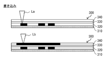
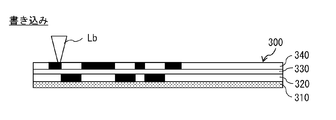
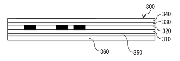
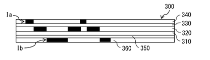
- FIG. 1 It is a figure which shows the cross-sectional composition example of the data protection sticker which concerns on 1st Embodiment of this disclosure. It is a figure which shows the state that the data protection sticker of FIG. 1 is attached to a document. It is a figure which shows the schematic configuration example of the drawing apparatus which draws on the data protection sticker of FIG. It is a figure which shows the schematic structure example of the scanner part of FIG. It is a figure which shows an example of writing and erasing on a data protection sticker using the drawing apparatus of FIG. It is a figure which shows one modification of the writing of FIG. It is a figure which shows one modification of the writing of FIG. It is a figure which shows one modification of the writing of FIG. It is a figure which shows one modification of the cross-sectional structure of the data protection sticker of FIG.
- FIGS. 1 to 5 Example of providing one cover layer on the data protection sticker 2.
- Modification example of the first embodiment Modification A (FIGS. 6 and 7) Example of writing inverted image data and image data of a complicated pattern to the cover layer Modification B
- Example of using a phase change material for the cover layer Deformation example D (FIGS. 8 to 11)
- Example of providing two cover layers on the data protection sticker Deformation example E (FIGS.
- FIG. 28 Example of providing one cover layer on the card 6.
- Modification example of the third embodiment Modification L (FIG. 29) Example where the data layer is irreversible 7.
- Deformation example common to each embodiment Deformation example M (FIGS. 30 to 32)
- Deformation example N (FIGS. 33 to 35)
- Example of providing a water vapor barrier layer and an ultraviolet ray blocking layer on a document Deformation example O (FIGS. 36 to 38)
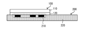
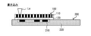
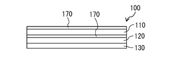
- FIG. 1 shows a schematic configuration example of the data protection sticker 100 according to the present embodiment.
- the data protection sticker 100 is a layer that protects the data layer 210 (described later) in which confidential information is recorded as a visible image.
- the data protection sticker 100 includes, for example, a cover layer 110, an adhesive layer 120, and a protective layer 130.
- the cover layer 110, the adhesive layer 120, and the protective layer 130 are laminated in this order.
- the adhesive layer 120 and the protective layer 130 are provided at positions facing the cover layer 110.
- the protective layer 130 is a layer that protects the adhesive layer 120, and is peeled off from the adhesive layer 120 when the data protection sticker 100 is used.
- the protective layer 130 is a flexible resin layer, and is formed of, for example, polyethylene terephthalate (PET) or the like.
- PET polyethylene terephthalate
- the adhesive layer 120 is a layer for attaching the data protection sticker 100 to, for example, a document, and is formed of, for example, an acrylic adhesive.
- the cover layer 110 is a layer for blindfolding the confidential information recorded on the document or the like (hereinafter, simply referred to as "confidential information") by attaching the cover layer 110 to the document or the like.
- the cover layer 110 is configured to be capable of transitioning between a color development state and a decolorization state in the visible wavelength range.
- the color of the cover layer 110 at the time of color development is preferably black with an optical density of 1.5 or more.
- the optical density of the color of the cover layer 110 at the time of color development may be such that the visible image of the data layer 210 cannot be visually recognized.
- the visible image of the cover layer 110 may be composed of multiple colors or may be composed of a single color.
- the cover layer 110 When the cover layer 110 attached to a document or the like is in a colored state in the visible wavelength range, the cover layer 110 hinders the visual recognition or recognition of confidential information. When the cover layer 110 hinders the visibility of the confidential information, all or part of the confidential information is invisible by the cover layer 110. On the other hand, when the cover layer 110 hinders the recognition of the confidential information, although all or part of the confidential information is visible through the cover layer 110, the confidential information is stored by the cover layer 110. It looks like a visible image that is different from the original visible image.
- the cover layer 110 attached to a document or the like when the cover layer 110 attached to a document or the like is in a decolorized state in the visible wavelength range, the cover layer 110 does not interfere with the visibility of confidential information. At this time, the confidential information is visible through the cover layer 110.
- the cover layer 110 is composed of, for example, a leuco dye (reversible heat-sensitive color-developing composition) and a photothermal converter that generates heat during writing.
- the cover layer 110 is further composed of, for example, a color developer and a polymer.
- the leuco dye combines with a developer to develop a color in the visible wavelength range, or separates from the developer to cause a decolorization in the visible wavelength range.
- the cover layer 110 reaches the writing temperature due to heat, for example, the leuco dye contained in the cover layer 110 develops a predetermined color in the visible wavelength range by combining with a developer. Further, the cover layer 110 becomes transparent in the visible wavelength region in the decolorized state.
- the photothermal converter absorbs light in the near infrared region (700 nm to 2500 nm) and generates heat, for example. In the present specification, the near-infrared region refers to a wavelength band of 700 nm to 2500 nm.
- the photothermal converter contained in the cover layer 110 has, for example, an absorption peak at a wavelength of ⁇ 1 (700 nm ⁇ ⁇ 1 ⁇ 2500 nm).
- FIG. 2 shows how the data protection sticker 100 is attached to the document 200.
- the protective layer 130 is peeled off from the adhesive layer 120, and the cover layer 110 is attached to the data layer 210 of the document 200 by the adhesive layer 120.
- Document 200 includes a base material layer 220 and a data layer 210 in which confidential information is recorded as a visible image.
- the base material layer 220 is made of an opaque material such as paper.
- the data layer 210 is, for example, a printing layer in which confidential information is irreversibly fixed on the base material layer 220, and is composed of, for example, a visible image formed by offset printing.
- the data layer 210 may be characters or pictures written by hand on the base material layer 220.
- the data layer 210 is composed of visible images such as numbers, characters, barcodes, two-dimensional codes, photographs and figures.
- FIG. 3 shows a schematic configuration example of the drawing device 1 that writes and erases the data protection sticker 100 on the cover layer 110.
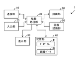
- the drawing device 1 includes, for example, a communication unit 10, an input unit 20, a display unit 30, a storage unit 40, an image recognition unit 50, a drawing unit 60, and an information processing unit 70.
- the drawing device 1 is connected to the network via the communication unit 10.
- the network is, for example, a communication line such as LAN or WAN.
- a terminal device is connected to the network.
- the drawing device 1 is configured to be able to communicate with the terminal device via a network.
- the terminal device is, for example, a mobile terminal, and is configured to be able to communicate with the drawing device 1 via a network.
- the communication unit 10 communicates with an external device such as a terminal device.
- the communication unit 10 outputs one or more input image data received from an external device such as a mobile terminal to the information processing unit 70, for example.
- the information processing unit 70 stores one or a plurality of input image data input from the communication unit 10 in the storage unit 40.
- the one or more input image data is, for example, data in which the gradation value of each drawing coordinate is described.
- the input unit 20 receives input from the user (for example, an execution instruction).
- the input unit 20 outputs the information input by the user to the information processing unit 70.
- the information processing unit 70 executes a predetermined process based on the information input from the input unit 20.
- the display unit 30 displays the screen based on various screen data created by the information processing unit 70.
- the display unit 30 is composed of, for example, a liquid crystal panel, an organic EL (Electro Luminescence) panel, or the like.
- the image recognition unit 50 performs measurement in response to a measurement command from the information processing unit 70.
- the image recognition unit 50 acquires the visible image data of the data layer 210, for example, by measuring the surface of the data layer 210.
- the visible image data is, for example, data in which the gradation value of each drawing coordinate is described.
- the image recognition unit 50 outputs the visible image data obtained by measuring the surface of the data layer 210 to the information processing unit 70.
- the information processing unit 70 stores the visible image data input from the image recognition unit 50 in the storage unit 40.
- the storage unit 40 stores, for example, the program 41 and the image data 42.
- Program 41 includes a series of steps for writing and erasing the data protection sticker 100 on the cover layer 110.
- the image data 42 is, for example, data in which gradation values of each drawing coordinate are described, and is image data used when writing to the data protection sticker 100 and an image used when erasing the data protection sticker 100. Includes data.
- the image data 42 may be image data used for both writing and erasing the data protection sticker 100.
- the information processing unit 70 writes or erases the cover layer 110 when the program 41 is loaded. For example, one or more input image data input from the communication unit 10 and visible image data input from the image recognition unit 50 are stored in the storage unit 40. One or more input image data or visible image data may also be used when writing to the cover layer 110.
- the information processing unit 70 includes, for example, a CPU (Central Processing Unit) and a GPU (Graphics Processing Unit).
- the information processing unit 70 executes, for example, the program 41 stored in the storage unit 40. The execution of the program 41 in the information processing unit 70 will be described in detail later.
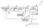
- FIG. 4 shows a schematic configuration example of the drawing unit 60.
- the drawing unit 60 includes, for example, a signal processing circuit 61, a laser drive circuit 62, a light source unit 63, an adjustment mechanism 64, a scanner drive circuit 65, and a scanner unit 66.
- the drawing unit 60 writes or erases the cover layer 110 by controlling the output of the light source unit 63 based on the output set value input from the information processing unit 70.
- the output set value is, for example, a command voltage value corresponding to the gradation value of each drawing coordinate of the image data 42, one or a plurality of input image data or the visible image data.
- the signal processing circuit 61 acquires an output set value input from the information processing unit 70 as an image signal Din.
- the signal processing circuit 61 generates, for example, a pixel signal Dout corresponding to the scanner operation of the scanner unit 66 from the image signal Din.
- the pixel signal Dout causes the light source unit 63 to output a laser beam having a power corresponding to the output set value.
- the signal processing circuit 61 together with the laser drive circuit 62, controls the peak value of the current pulse applied to the light source unit 63 (light source 63A) according to the pixel signal Dout.
- the laser drive circuit 62 drives the light source 63A of the light source unit 63 according to the pixel signal Dout, for example.
- the laser drive circuit 62 controls the brightness (brightness) of the laser beam, for example, in order to draw an image corresponding to the pixel signal Dout.
- the laser drive circuit 62 has, for example, a drive circuit that drives the light source 63A.
- the light source 63A writes and erases the data protection sticker 100 by outputting a laser beam having a power corresponding to the output set value to the data protection sticker 100.
- the light source 63A emits a laser beam in the near infrared region.
- the light source 63A is, for example, a semiconductor laser that emits a laser beam La having a wavelength of ⁇ 1.
- the light source unit 63 has, for example, a light source 63A and a lens 63e.
- the adjustment mechanism 64 is a mechanism for adjusting the focus of the light (laser beam La) emitted from the light source unit 63.
- the adjustment mechanism 64 is, for example, a mechanism for adjusting the position of the lens 63e by a manual operation by the user.
- the adjusting mechanism 64 may be a mechanism for adjusting the position of the lens 63e by a mechanical operation.
- the scanner drive circuit 65 drives the scanner unit 66 in synchronization with, for example, the projected video clock signal input from the signal processing circuit 61. Further, when a signal about the irradiation angle of the two-axis scanner 66A described later is input from the scanner unit 66, for example, the scanner drive circuit 65 is set to a desired irradiation angle based on the signal. Drives the scanner unit 66.
- the scanner unit 66 causes, for example, raster scan the light (laser beam La) incident from the light source unit 63 on the surface of the data protection sticker 100.
- the scanner unit 66 has, for example, a biaxial scanner 66A and an f ⁇ lens 66B.
- the 2-axis scanner 66A is, for example, a galvano mirror.
- the f ⁇ lens 66B converts the constant velocity rotational scan by the biaxial scanner 66A into a constant velocity linear scan of a spot moving on the focal plane (the surface of the data protection seal 100).
- the scanner unit 66 may be composed of a 1-axis scanner and an f ⁇ lens. In this case, it is preferable that the data protection sticker 100 is provided with a uniaxial stage that displaces the data protection sticker 100 in a direction orthogonal to the scanning direction of the uniaxial scanner.
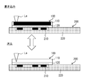
- the user prepares the uncolored data protection sticker 100 and sets it in the drawing unit 60.
- the user instructs the information processing unit 70 to write via the input unit 20.
- the information processing unit 70 converts the image data 42 read from the storage unit 40 into the output setting value of the drawing unit 60, and inputs the output setting value obtained by the conversion to the drawing unit 60.
- the drawing unit 60 writes to the data protection sticker 100 based on the input output set value (see the upper diagram of FIG. 5).
- the signal processing circuit 61 of the drawing unit 60 acquires the output set value input from the information processing unit 70 as an image signal Din.
- the signal processing circuit 61 synchronizes with the scanner operation of the scanner unit 66 from the image signal Din and generates a light emitting signal according to the characteristics such as the wavelength of the laser beam.
- the signal processing circuit 61 outputs the generated light emission signal to the laser drive circuit 62 of the drawing unit 60.
- the laser drive circuit 62 drives the light source 63A of the light source unit 63 according to the light emission signal. At this time, the laser drive circuit 62 emits the laser beam La from the light source 63A and scans it on the data protection sticker 100, for example.
- the laser beam La having a wavelength of ⁇ 1 is absorbed by the photothermal converter in the cover layer 110, so that the cover layer 110 reaches the writing temperature due to the heat generated from the photothermal converter, and the leuco dye is colored. Combines with the agent to develop a predetermined color in the visible wavelength range. In this way, the drawing unit 60 writes to the data protection sticker 100.
- the user prepares the data protection sticker 100 written as described above and sets it in the drawing unit 60.
- the user instructs the information processing unit 70 to erase via the input unit 20.
- the information processing unit 70 sets the output set value so that the temperature of the cover layer 110 to be erased becomes a temperature condition suitable for erasing due to heat generated by the photothermal converter.
- the drawing unit 60 erases the data protection sticker 100 based on the input output set value (see the lower diagram of FIG. 5).
- the signal processing circuit 61 of the drawing unit 60 acquires the output set value input from the information processing unit 70 as an image signal Din.
- the signal processing circuit 61 generates a light emitting signal from the image signal Din in synchronization with the scanner operation of the scanner unit 66 and corresponds to characteristics such as the wavelength of the laser light, and outputs the light emission signal to the laser drive circuit 62 of the drawing unit 60.
- the laser drive circuit 62 drives the light source 63A of the light source unit 63 according to the light emission signal. At this time, the laser drive circuit 62 emits the laser beam La from the light source 63A and scans it on the data protection sticker 100, for example. As a result, for example, the laser beam La having a wavelength of ⁇ 1 is absorbed by the photothermal converter in the cover layer 110, whereby the heat generated from the photothermal converter makes the cover layer 110 a temperature condition suitable for decolorization, and the leuco dye. Separates from the developer and decolorizes. In this way, the drawing unit 60 erases the data protection sticker 100.
- the data protection seal 100 is attached to the data layer 210 to develop a color of the cover layer 110 to make the confidential information invisible, or the cover layer 110 recognizes the confidential information.
- Confidential information can be concealed by hindering. Further, by erasing the cover layer 110 and visualizing the confidential information, the confidential information can be visually recognized in the visible wavelength range. Therefore, in the data protection sticker 100 according to the present embodiment, the confidential information can be visualized in the visible wavelength region.
- the protective layer 130 that protects the adhesive layer 120 is provided. This makes it easier to handle the data protection sticker 100 as compared with the case where the protection layer 130 is not provided.
- the cover layer 110 is composed of a leuco dye, a photothermal converter, a color developer, and a polymer.
- the cover layer 110 is irradiated with a laser beam having an emission wavelength corresponding to the absorption wavelength of the photothermal converter to generate heat of the photothermal converter, so that the cover layer 110 reaches the writing temperature, and the color developer and the leuco dye are used. Can combine with each other to bring the leuco dye into a colored state in the visible wavelength range.
- the cover layer 110 is colored to make the data layer 210 invisible, or the cover layer 110 hinders the recognition of the confidential information, so that the confidential information can be concealed.
- the cover layer 110 when the cover layer 110 is set to a temperature condition suitable for decolorization by heat generation due to laser irradiation, the developer and the leuco dye are separated from each other, and the leuco dye can be decolorized in the visible wavelength range. As a result, the visible image of the cover layer 110 is erased, the cover layer 110 is in the decolorized state, and the data layer 210 is in the visible state, so that the confidential information can be visually recognized in the visible wavelength range.
- the data layer 210 is a printing layer in which confidential information is irreversibly fixed on the base material layer 220.
- the confidential information printed on the data layer 210 can be visually recognized in the visible wavelength range.
- the drawing apparatus 1 by irradiating the cover layer 110 with the laser beam La emitted from the light source unit 63, either writing or erasing of the cover layer 110 is performed.
- the confidential information of the data layer 210 can be made invisible, or the cover layer 110 hinders the recognition of the confidential information, so that the confidential information can be concealed. ..
- the data layer 210 is visualized and the confidential information can be visually recognized. Therefore, in the drawing apparatus 1 according to the present embodiment, the confidential information can be visualized in the visible wavelength region.
- the information processing unit 70 obtains the visible image data read from the storage unit 40 by performing predetermined processing.
- the processed image data may be converted into the image data of the cover layer 110.
- the processed image data is, for example, a shade image data having a pattern different from the pattern of the visible image data of the data layer 210.
- it may be inverted image data in which visible image data is inverted as shown in FIG. 6, or may be image data having a complicated pattern as shown in FIG. 7, for example. ..
- the entire confidential information is in a visible state via the cover layer 110.
- the confidential information looks like a visible image (for example, a solid image) different from the original visible image of the confidential information due to the cover layer 110.
- image data having a complicated pattern as shown in FIG. 7 is written to the cover layer 110, a part of the confidential information is visible through the cover layer 110.
- the cover layer 110 makes the confidential information look like a visible image (for example, a striped image) different from the original visible image of the confidential information. Therefore, by writing to the cover layer 110, the confidential information can be blindfolded by the cover layer 110 as in the above embodiment. On the other hand, by erasing the cover layer 110, the confidential information can be visually recognized through the cover layer 110 as in the above embodiment.
- the cover layer 110 may be configured to include, for example, a photochromic material.
- the photochromic material include a diarylethene compound and the like.
- the photochromic material is configured so that it can transition between a color development state (coloring state) and a decolorization state in the visible wavelength range.
- the photochromic material has an absorption peak in the ultraviolet region in the decolorized state, and when irradiated with ultraviolet rays having a wavelength near the absorption peak, the absorption peak shifts to the visible light region and becomes a colored state.
- the photochromic material is colored to make the cover layer 110 invisible, or the cover layer 110 hinders the recognition of confidential information. Confidential information can be concealed. Further, by irradiating strong visible light close to the absorption peak wavelength in the color-developed state to decolorize the photochromic material and visualizing the cover layer 110, confidential information can be visually recognized. Therefore, even in the data protection sticker 100 according to this modification, the confidential information can be visualized in the visible wavelength range.
- the cover layer 110 is, for example, a material whose light transmittance in the visible wavelength region can be controlled by a phase change, or a color-developed state and a decolorized state in the visible wavelength region by a phase change. It may be composed of a material that can be changed. As such a material, a phase change material capable of transitioning between two phases, amorphous and crystalline, can be used. For example, a germanium-antimony tellurium alloy Ge 2 Sb 2 Te 5 film becomes a transparent amorphous phase when heated to a high temperature of about 600 ° C. and rapidly cooled, and becomes an opaque crystal when heated to a medium temperature of about 160 ° C. and slowly cooled.
- the amorphous phase can be made into a visible state of confidential information, and the crystalline phase can be made into an invisible state of confidential information.
- the confidential information can be concealed by changing the phase changing material to a crystalline phase to make the cover layer 110 opaque, or by the cover layer 110 hindering the recognition of the confidential information. Further, by changing the phase changing material to an amorphous phase and making the cover layer 110 transparent, the confidential information can be visually recognized. Therefore, even in the data protection sticker 100 according to this modification, the confidential information can be visualized in the visible wavelength range.
- the data protection seal 100 may include one or more cover layers having the same functions as the cover layer 110 in addition to the cover layer 110.
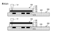
- the data protection sticker 100 may include cover layers 110 and 140, for example, as shown in FIG.
- the data protection sticker 100 may include an adhesive heat insulating layer 150 between the cover layer 110 and the cover layer 140.
- the adhesive heat insulating layer 150 is a layer of an adhesive or an adhesive for adhering the cover layer 140 to the cover layer 110, and is a layer that prevents heat from propagating between the cover layer 110 and the cover layer 140. ..
- the adhesive heat insulating layer 150 is made of, for example, an adhesive or an adhesive made of a synthetic resin having a thermal conductivity of 0.3 (W / m ⁇ K) or less.
- the thickness of the adhesive heat insulating layer 150 is preferably 3 ⁇ m or more, and more preferably 6 ⁇ m or more.
- the cover layer 140 is a layer for blindfolding confidential information by attaching it to a document or the like.
- the cover layer 140 is configured to be capable of transitioning between a color development state and a decolorization state in the visible wavelength range.
- the color of the cover layer 140 at the time of color development is preferably black with an optical density of 1.5 or more.
- the optical density of the color of the cover layer 140 at the time of color development may be such that the visible image of the data layer 210 cannot be visually recognized.
- the visible image of the cover layer 140 may be composed of multiple colors or may be composed of a single color. When the visible image of the data layer 210 is a single color, the color difference ⁇ E * between the data layer 210 and the cover layer 110 is preferably 1.2 or less.
- the color difference ⁇ E * between the data layer 210 and the cover layer 110 may be such that the visible image of the data layer 210 cannot be visually recognized.
- the above color difference ⁇ E * has two colors (L * 1 , a * 1 , b * 1 ) and (L * 2 , a * 2 , b * 2 ) in the L * a * b * color space.
- the cover layer 140 When the cover layer 140 attached to a document or the like is in a colored state in the visible wavelength range, the cover layer 140 hinders the visual recognition or recognition of confidential information. When the cover layer 140 obstructs the visibility of the confidential information, all or part of the confidential information is invisible by the cover layer 140. On the other hand, when the cover layer 140 hinders the recognition of the confidential information, the confidential information is visible by the cover layer 140, although all or part of the confidential information is visible through the cover layer 140. It looks like a visible image that is different from the original visible image.
- the cover layer 140 attached to a document or the like when the cover layer 140 attached to a document or the like is in a decolorized state in the visible wavelength range, the cover layer 140 does not interfere with the visibility of confidential information. At this time, the confidential information is visible through the cover layer 140.
- the cover layer 140 is composed of, for example, a leuco dye and a photothermal converter that generates heat during writing.
- the cover layer 140 is further composed of, for example, a color developer and a polymer.
- the leuco dye combines with a developer to develop a color in the visible wavelength range, or separates from the developer to cause a decolorization in the visible wavelength range.
- the cover layer 140 reaches the writing temperature due to heat, for example, the leuco dye contained in the cover layer 140 develops a predetermined color in the visible wavelength range by combining with a developer. Further, the cover layer 140 becomes transparent in the visible wavelength region in the decolorized state.
- the photothermal converter absorbs light in the near infrared region (700 nm to 2500 nm) and generates heat, for example.
- the photothermal converter contained in the cover layer 140 has, for example, an absorption peak at a wavelength of ⁇ 2 ( ⁇ 2 ⁇ ⁇ 1, 700 nm ⁇ ⁇ 2 ⁇ 2500 nm).
- the wavelength ⁇ 1 of the absorption peak of the photothermal converter contained in the cover layer 110 is included in the cover layer 140. It is preferable that the wavelength is longer than the wavelength ⁇ 2 of the absorption peak of the photothermal converter. This is because, for example, when writing or erasing the cover layer 110 via the cover layer 140 by using the drawing device 1 provided with the drawing unit 60 of FIG. 9 described later, the laser beam having a wavelength ⁇ 1 is emitted from the cover layer 140. This is to make it difficult to be absorbed by.
- FIG. 9 shows a schematic configuration example of the drawing unit 60 that writes and erases the data protection sticker 100 shown in FIG.
- the drawing unit 60 includes, for example, a signal processing circuit 61, a laser drive circuit 62, a light source unit 63, an adjustment mechanism 64, a scanner drive circuit 65, and a scanner unit 66.
- the drawing unit 60 executes drawing on the data protection sticker 100 by controlling the output of the light source unit 63 based on the output setting value input from the information processing unit 70.
- the signal processing circuit 61 acquires an output set value input from the information processing unit 70 as an image signal Din.
- the signal processing circuit 61 generates, for example, a pixel signal Dout corresponding to the scanner operation of the scanner unit 66 from the image signal Din.
- the pixel signal Dout causes the light source unit 63 (for example, the light sources 63A and 63B described later) to output a laser beam having a power corresponding to the output set value.
- the signal processing circuit 61 together with the laser drive circuit 62, controls the peak value of the current pulse applied to the light source unit 63 (for example, the light sources 63A and 63B) according to the pixel signal Dout.
- the laser drive circuit 62 drives the light sources 63A and 63B of the light source unit 63 according to the pixel signal Dout, for example.
- the laser drive circuit 62 controls the brightness (brightness) of the laser beam, for example, in order to draw an image corresponding to the pixel signal Dout.
- the laser drive circuit 62 includes, for example, a drive circuit 62A for driving the light source 63A and a drive circuit 62B for driving the light source 63B.
- the light sources 63A and 63B output the laser beam of the power corresponding to the output set value to the data protection sticker 100 to write and erase the data protection sticker 100.
- the light sources 63A and 63B emit laser light in the near infrared region.
- the light source 63A is, for example, a semiconductor laser that emits a laser beam La having a wavelength of ⁇ 1.
- the light source 63B is, for example, a semiconductor laser that emits a laser beam Lb having a wavelength of ⁇ 2.
- the light source unit 63 has a plurality of light sources having different emission wavelengths in the near infrared region.
- the light source unit 63 has, for example, two light sources 63A and 63B.
- the light source unit 63 further has, for example, an optical system that combines laser beams emitted from a plurality of light sources (for example, two light sources 63A and 63B).
- the light source unit 63 has, for example, a reflection mirror 63a, a dichroic mirror 63b, and a lens 63e as such an optical system.
- the laser beams La and Lb emitted from the two light sources 63A and 63B are made into substantially parallel light (colimated light) by, for example, a collimating lens. After that, for example, the laser beam La is reflected by the reflection mirror 63a and reflected by the dichroic mirror 63b, and the laser beam Lb is transmitted through the dichroic mirror 63b so that the laser beam La and the laser beam La are combined. To.
- the combined wave light Lm of the laser light La and the laser light La passes through the dichroic mirror 63c.
- the light source unit 63 outputs the combined wave light Lm obtained by the combined wave by the above optical system to the scanner unit 66.
- the adjustment mechanism 64 is a mechanism for adjusting the focus of the combined wave light Lm emitted from the light source unit 63.
- the adjustment mechanism 64 is, for example, a mechanism for adjusting the position of the lens 63e by a manual operation by the user.
- the adjusting mechanism 64 may be a mechanism for adjusting the position of the lens 63e by a mechanical operation.
- the scanner drive circuit 65 drives the scanner unit 66 in synchronization with, for example, the projected video clock signal input from the signal processing circuit 61. Further, in the scanner drive circuit 65, for example, when a signal about the irradiation angle of the 2-axis scanner 66A or the like is input from the scanner unit 66, the scanner unit so as to obtain a desired irradiation angle based on the signal. Drive 66.
- the scanner unit 66 causes, for example, raster scan the combined wave light Lm incident from the light source unit 63 on the surface of the data protection sticker 100.
- the scanner unit 66 has, for example, a biaxial scanner 66A and an f ⁇ lens 66B.
- the 2-axis scanner 66A is, for example, a galvano mirror.
- the f ⁇ lens 66B converts the constant velocity rotational scan by the biaxial scanner 66A into a constant velocity linear scan of a spot moving on the focal plane (the surface of the data protection seal 100).
- the scanner unit 66 may be composed of a 1-axis scanner and an f ⁇ lens. In this case, it is preferable that the data protection sticker 100 is provided with a uniaxial stage that displaces the data protection sticker 100 in a direction orthogonal to the scanning direction of the uniaxial scanner.
- the user prepares the uncolored data protection sticker 100 and sets it in the drawing unit 60.
- the user instructs the information processing unit 70 to write via the input unit 20.
- the information processing unit 70 converts the image data 42 read from the storage unit 40 into the output setting value of the drawing unit 60, and inputs the output setting value obtained by the conversion to the drawing unit 60.
- the drawing unit 60 writes to the cover layers 110 and 140 of the data protection sticker 100 based on the input output set value.
- the signal processing circuit 61 of the drawing unit 60 acquires the output set value input from the information processing unit 70 as an image signal Din.
- the signal processing circuit 61 synchronizes with the scanner operation of the scanner unit 66 from the image signal Din and generates a light emitting signal according to the characteristics such as the wavelength of the laser beam.
- the signal processing circuit 61 outputs the generated light emission signal to the laser drive circuit 62 of the drawing unit 60.
- the laser drive circuit 62 drives the light sources 63A and 63B of the light source unit 63 according to the light emission signal. At this time, the laser drive circuit 62 emits the laser beam La from the light source 63A, emits the laser beam Lb from the light source 63B, and scans the combined light Lm on the data protection sticker 100. As a result, the laser beam La of the wavelength ⁇ 1 contained in the synthetic light Lm is absorbed by the photothermal converter in the cover layer 110, so that the cover layer 110 reaches the writing temperature due to the heat generated from the photothermal converter.
- the leuco dye combines with the color developer to develop a predetermined color in the visible wavelength range (upper part of FIG. 10).
- the laser beam Lb having a wavelength of ⁇ 2 contained in the synthetic light Lm is absorbed by the photothermal converter in the cover layer 140, whereby the cover layer 140 reaches the writing temperature due to the heat generated from the photothermal converter, and the leuco The dye combines with the developer to develop a predetermined color in the visible wavelength range (lower figure of FIG. 10). In this way, the drawing unit 60 writes to the data protection sticker 100 shown in FIG.
- the user prepares the data protection sticker 100 written as described above and sets it in the drawing unit 60.
- the user instructs the information processing unit 70 to erase via the input unit 20.
- the information processing unit 70 sets the output set value so that the temperature of the cover layers 110 and 140 to be erased becomes a temperature condition suitable for erasing due to heat generated by the photothermal converter.
- the drawing unit 60 erases the data protection sticker 100 based on the input output set value.
- the signal processing circuit 61 of the drawing unit 60 acquires the output set value input from the information processing unit 70 as an image signal Din.
- the signal processing circuit 61 generates a light emitting signal from the image signal Din in synchronization with the scanner operation of the scanner unit 66 and corresponds to characteristics such as the wavelength of the laser light, and outputs the light emission signal to the laser drive circuit 62 of the drawing unit 60.
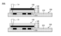
- the laser drive circuit 62 drives the light sources 63A and 63B of the light source unit 63 according to the light emission signal. At this time, the laser drive circuit 62 emits the laser beam La from the light source 63A, emits the laser beam Lb from the light source 63B, and scans the combined light Lm on the data protection sticker 100. As a result, the laser beam La of the wavelength ⁇ 1 contained in the synthetic light Lm is absorbed by the photothermal converter in the cover layer 110, whereby the temperature at which the cover layer 110 is suitable for decoloring due to the heat generated from the photothermal converter. As a condition, the leuco dye separates from the developer and decolorizes (upper part of FIG. 11).
- the laser beam Lb having a wavelength of ⁇ 2 contained in the synthetic light Lm is absorbed by the photothermal converter in the cover layer 140, so that the cover layer 140 is suitable for decoloring due to the heat generated from the photothermal converter.
- the leuco dye separates from the developer and decolorizes (lower figure of FIG. 11). In this way, the drawing unit 60 erases the data protection sticker 100.
- the data protection seal 100 is attached to the data layer 210, and the cover layers 110 and 140 are colored to make the confidential information invisible, or the cover layers 110 and 140 are used for the confidential information. Confidential information can be concealed by hindering recognition. Further, by erasing the cover layers 110 and 140 to visualize the confidential information, the confidential information can be visually recognized in the visible wavelength range. Therefore, in the data protection sticker 100 according to the present modification, the confidential information can be visualized in the visible wavelength region.
- the cover layers 110 and 140 are composed of a leuco dye, a photothermal converter, a color developer, and a polymer.
- the cover layers 110 and 140 are irradiated with laser light having an emission wavelength corresponding to the absorption wavelength of the photothermal converter to generate heat of the photothermal converter, so that the cover layers 110 and 140 reach the writing temperature and develop color.
- the agent and the leuco dye can bind to each other to bring the leuco dye into a colored state in the visible wavelength range.
- the cover layers 110 and 140 are colored to make the data layer 210 invisible, and the cover layers 110 and 140 hinder the recognition of the confidential information, so that the confidential information can be concealed.
- the cover layers 110 and 140 are set to temperature conditions suitable for decolorization due to heat generated by laser irradiation, the developer and the leuco dye are separated from each other, and the leuco dye can be decolorized in the visible wavelength range. it can. As a result, the visible images of the cover layers 110 and 140 are erased, and by putting the cover layers 110 and 140 in a decolorized state and making the data layer 210 visible, the confidential information can be visually recognized in the visible wavelength range.
- the drawing apparatus 1 by irradiating the cover layer 110 with the synthetic light Lm emitted from the light source unit 63, either writing or erasing of the cover layers 110 or 140 is performed. ..
- the confidential information of the data layer 210 is made invisible, and the cover layers 110 and 140 hinder the recognition of the confidential information.
- Confidential information can be concealed.
- the data layer 210 is visualized and the confidential information can be visually recognized. Therefore, in the drawing apparatus 1 according to the present modification, the confidential information can be visualized in the visible wavelength region.
- the adhesive heat insulating layer 150 is provided between the cover layer 110 and the cover layer 140, the adhesive heat insulating layer 150 hinders heat propagation between the cover layer 110 and the cover layer 140. Be done. Thereby, for example, when the cover layer 110 is being colored or decolorized, it is possible to prevent the cover layer 140 from being erroneously developed or decolorized.
- the reversible data layer 230 may be provided in the document 200 instead of the data layer 210.
- the reversible data layer 230 is configured so that confidential information can be recorded as a visible image, and is configured to include, for example, a reversible material capable of transitioning between a color development state and a decolorization state in the visible wavelength range. Confidential information is recorded as a visible image on the reversible data layer 230.
- the confidential information is recorded in the reversible data layer 230 as a visible image by the color development of the reversible material described above.
- the optical density of the color of the cover layer 110 at the time of color development may be such that the visible image of the reversible data layer 230 cannot be visually recognized.
- the visible image of the cover layer 110 may be composed of multiple colors or may be composed of a single color.
- the color difference ⁇ E * between the reversible data layer 230 and the cover layer 110 is preferably 1.2 or less.
- the color difference ⁇ E * between the data layer 210 and the cover layer 110 may be such that the visible image of the data layer 210 cannot be visually recognized.
- the reversible data layer 230 is composed of, for example, a leuco dye and a photothermal converter that generates heat during writing.
- the reversible data layer 230 is further configured to include, for example, a color developer and a polymer.
- the leuco dye combines with a developer to develop a color in the visible wavelength range, or separates from the developer to cause a decolorization in the visible wavelength range.
- the leuco dye contained in the reversible data layer 230 develops a predetermined color in the visible wavelength region by combining with a developer when the reversible data layer 230 reaches the writing temperature due to heat, for example. Further, the reversible data layer 230 becomes transparent in the visible wavelength region in the decolorized state.
- the photothermal converter absorbs light in the near infrared region (700 nm to 2500 nm) and generates heat, for example.
- the photothermal converter contained in the reversible data layer 230 has, for example, an absorption peak at wavelength ⁇ 2.
- the cover layer 110 is configured to be a reversible material having different transition conditions from the reversible data layer 230.
- the cover layer 110 is colored or decolorized when irradiated with a laser beam having a wavelength ⁇ 1 and the reversible data layer 230 is colored or decolorized when irradiated with a laser beam having a wavelength ⁇ 2.
- the wavelength ⁇ 2 of the absorption peak of the photothermal converter contained in the reversible data layer 230 is the wavelength ⁇ 2 of the photothermal converter contained in the cover layer 110. It is preferable that the wavelength is longer than the wavelength ⁇ 1 of the absorption peak of.
- the wavelength ⁇ 1 of the absorption peak of the photothermal converter contained in the cover layer 110 is preferably shorter than the wavelength ⁇ 2 of the absorption peak of the photothermal converter contained in the reversible data layer 230. This is because, for example, when the drawing device 1 provided with the drawing unit 60 of FIG. 9 is used to write or erase the reversible data layer 230 via the cover layer 110, the laser beam having a wavelength of ⁇ 2 is applied to the cover layer 110. This is to make it difficult to be absorbed by.
- the adhesive layer 120 is a layer for adhering the cover layer 110 to the reversible data layer 230, and also prevents heat from propagating between the cover layer 110 and the reversible data layer 230. It is preferably a heat insulating layer.
- the pressure-sensitive adhesive layer 120 is composed of, for example, a pressure-sensitive adhesive or an adhesive made of a synthetic resin having a thermal conductivity of 0.3 (W / m ⁇ K) or less.
- the thickness of the adhesive heat insulating layer 150 is preferably 3 ⁇ m or more, and more preferably 6 ⁇ m or more.
- the user prepares the uncolored reversible data layer 230 and the data protection sticker 100, and sets them in the drawing unit 60.
- the user instructs the information processing unit 70 to write via the input unit 20.
- the information processing unit 70 converts the two input image data read from the storage unit 40 into the output setting values of the drawing unit 60, and inputs the two output setting values obtained by the conversion to the drawing unit 60.
- the drawing unit 60 writes to the reversible data layer 230 and the data protection sticker 100 based on the two input output setting values.
- the signal processing circuit 61 of the drawing unit 60 acquires the two output setting values input from the information processing unit 70 as the image signal Din.
- the signal processing circuit 61 synchronizes with the scanner operation of the scanner unit 66 from the image signal Din and generates a light emitting signal according to the characteristics such as the wavelength of the laser beam.
- the signal processing circuit 61 outputs the generated light emission signal to the laser drive circuit 62 of the drawing unit 60.
- the drive circuit 62A drives the light source 63A of the light source unit 63 according to the light emission signal generated from one of the output set values.
- the drive circuit 62B drives the light source 63B of the light source unit 63 according to the light emission signal generated from the other output set value.
- the drive circuit 62A emits the laser beam La from the light source 63A
- the drive circuit 62B emits the laser beam Lb from the light source 63B, and scans the combined light Lm on the data protection sticker 100.
- the laser beam La of the wavelength ⁇ 1 contained in the synthetic light Lm is absorbed by the photothermal converter in the cover layer 110, so that the cover layer 110 reaches the writing temperature due to the heat generated from the photothermal converter.
- the leuco dye combines with the color developer to develop a predetermined color in the visible wavelength range (lower figure of FIG. 13). Further, the laser beam Lb having a wavelength of ⁇ 2 contained in the synthetic light Lm is absorbed by the photothermal converter in the reversible data layer 230, whereby the heat generated from the photothermal converter causes the reversible data layer 230 to reach the writing temperature. Upon reaching it, the leuco dye combines with the developer to develop a predetermined color in the visible wavelength range (upper part of FIG. 13). In this way, the drawing unit 60 writes to the reversible data layer 230 and the data protection sticker 100 shown in FIG.
- the user prepares the reversible data layer 230 and the data protection sticker 100 written as described above, and sets them in the drawing unit 60.
- the user instructs the information processing unit 70 to erase the data protection sticker 100 via the input unit 20.
- the information processing unit 70 sets the output set value so that the temperature of the cover layer 110 to be erased becomes a temperature condition suitable for erasing due to heat generated by the photothermal converter.
- the drawing unit 60 erases the data protection sticker 100 based on the input output set value.
- the signal processing circuit 61 of the drawing unit 60 acquires the output set value input from the information processing unit 70 as an image signal Din.
- the signal processing circuit 61 generates a light emitting signal from the image signal Din in synchronization with the scanner operation of the scanner unit 66 and corresponds to characteristics such as the wavelength of the laser light, and outputs the light emission signal to the laser drive circuit 62 of the drawing unit 60.
- the laser drive circuit 62 drives the light source 63A of the light source unit 63 according to the light emission signal. At this time, the laser drive circuit 62 emits the laser beam La from, for example, the light source 63A, and scans the laser beam La on the data protection sticker 100. As a result, the laser beam La is absorbed by the photothermal converter in the cover layer 110, so that the heat generated from the photothermal converter makes the cover layer 110 a temperature condition suitable for decolorization, and the leuco dye is a developer. The color is erased separately from the above (upper part of FIG. 14). In this way, the drawing unit 60 erases the data protection sticker 100.
- the user may further instruct the information processing unit 70 to erase the reversible data layer 230 via the input unit 20.
- the information processing unit 70 converts the image data 42 read from the storage unit 40 into the output setting value of the drawing unit 60, and inputs the output setting value obtained by the conversion to the drawing unit 60.
- the information processing unit 70 sets the output set value so that the temperature of the reversible data layer 230 to be erased becomes a temperature condition suitable for erasing due to heat generated by the photothermal converter.
- the drawing unit 60 erases the reversible data layer 230 based on the input output set value.
- the signal processing circuit 61 of the drawing unit 60 acquires the output set value input from the information processing unit 70 as an image signal Din.
- the signal processing circuit 61 generates a light emitting signal from the image signal Din in synchronization with the scanner operation of the scanner unit 66 and corresponds to characteristics such as the wavelength of the laser light, and outputs the light emission signal to the laser drive circuit 62 of the drawing unit 60.
- the laser drive circuit 62 drives the light source 63B of the light source unit 63 according to the light emission signal. At this time, the laser drive circuit 62 emits the laser beam Lb from, for example, the light source 63B, and scans the laser beam Lb on the data protection sticker 100. As a result, the laser beam Lb is absorbed by the photothermal converter in the reversible data layer 230, whereby the heat generated from the photothermal converter makes the reversible data layer 230 a temperature condition suitable for decolorization, and the leuco dye. Separates from the developer and decolorizes (lower figure of FIG. 14). In this way, the drawing unit 60 erases the reversible data layer 230.
- the data protection seal 100 is attached to the reversible data layer 230, and the cover layer 110 is colored to make the confidential information invisible, or the cover layer 110 recognizes the confidential information. Confidential information can be concealed by hindering it. Further, by erasing the cover layer 110 and visualizing the confidential information, the confidential information can be visually recognized in the visible wavelength range. Therefore, in the data protection sticker 100 according to the present modification, the confidential information can be visualized in the visible wavelength region.
- the cover layer 110 is composed of a leuco dye, a photothermal converter, a color developer, and a polymer.
- the cover layer 110 is irradiated with a laser beam having an emission wavelength corresponding to the absorption wavelength of the photothermal converter to generate heat of the photothermal converter, so that the cover layer 110 reaches the writing temperature, and the color developer and the leuco dye are used.
- the cover layer 110 is colored to make the reversible data layer 230 invisible, and the cover layer 110 hinders the recognition of the confidential information, so that the confidential information can be concealed.
- the cover layer 110 when the cover layer 110 is set to a temperature condition suitable for decolorization by heat generation due to laser irradiation, the developer and the leuco dye are separated from each other, and the leuco dye can be decolorized in the visible wavelength range. As a result, the visible image of the cover layer 110 is erased, the cover layer 110 is in the decolorized state, and the reversible data layer 230 is in the visible state, so that the confidential information can be visually recognized in the visible wavelength range. Further, since the erasing process of the cover layer 110 requires a laser beam having a specific wavelength, it is possible to realize the data protection sticker 100 having a higher security level than the case of visualizing by simply raising the temperature.
- the reversible data layer 230 is configured to include a reversible material capable of transitioning between a color development state and a decolorization state in the visible wavelength region, like the cover layer 110.
- the reversible data layer 230 is configured to include a reversible material having different transition conditions from the cover layer 110.
- the cover layer 110 is configured to include a reversible material having different transition conditions from the reversible data layer 230.
- the drawing apparatus 1 can transition only the color development and decolorization of either the reversible data layer 230 or the cover layer 110.
- the visualization and invisibility of the confidential information can be controlled by transitioning only the color development and decolorization of the cover layer 110 by using the drawing device 1.
- the reversible data layer 230 can be rewritten by using the drawing device 1.
- the adhesive layer 120 when the adhesive layer 120 is the adhesive heat insulating layer described above, the adhesive layer 120 hinders heat propagation between the cover layer 110 and the reversible data layer 230. Thereby, for example, when the cover layer 110 is colored or decolorized, it is possible to prevent the reversible data layer 230 from being erroneously developed or decolorized.
- a protective layer 130 that protects the adhesive layer 120 is provided. This makes it easier to handle the data protection sticker 100 as compared with the case where the protection layer 130 is not provided.
- FIG. 15 shows a schematic configuration example of the document 300 according to the present embodiment.
- Document 300 includes, for example, a base material layer 310, a reversible data layer 320 formed on the base material layer 310, an adhesive heat insulating layer 330, and a cover layer 340.
- the reversible data layer 320, the adhesive heat insulating layer 330, and the cover layer 340 are laminated on the base material layer 310 in this order.
- the positions of the reversible data layer 320 and the cover layer 340 may be interchanged.
- the adhesive heat insulating layer 330 and the cover layer 340 are provided at positions facing the reversible data layer 320.
- the cover layer 340 is located above the reversible data layer 320.
- the base material layer 310 is made of an opaque material such as paper or synthetic resin.
- the adhesive heat insulating layer 330 is a layer for bonding the cover layer 340 to the reversible data layer 320, and is a layer that hinders heat propagation between the cover layer 340 and the reversible data layer 320.
- the adhesive heat insulating layer 330 is made of, for example, an adhesive or an adhesive made of a synthetic resin having a thermal conductivity of 0.3 (W / m ⁇ K) or less.
- the thickness of the adhesive heat insulating layer 330 is preferably 3 ⁇ m or more, and more preferably 6 ⁇ m or more.
- the reversible data layer 320 and the cover layer 340 are configured so that the color development state and the decolorization state in the visible wavelength range can be changed.
- the cover layer 340 is configured to include a reversible material having different transition conditions from the reversible data layer 320.
- the reversible data layer 320 is configured to include a reversible material having different transition conditions from the cover layer 340.
- the optical density of the color of the cover layer 340 at the time of color development may be such that the visible image of the reversible data layer 320 cannot be visually recognized.
- the visible image of the cover layer 340 may be composed of multiple colors or may be composed of a single color.
- the color difference ⁇ E * between the reversible data layer 320 and the cover layer 340 is preferably 1.2 or less.
- the color difference ⁇ E * between the reversible data layer 320 and the cover layer 340 may be such that the visible image of the reversible data layer 320 cannot be visually recognized.
- the cover layer 340 is a layer for blindfolding the confidential information written in the reversible data layer 320.
- the cover layer 340 hinders the visual recognition or recognition of confidential information.
- the cover layer 340 obstructs the visibility of the confidential information, all or part of the confidential information is invisible by the cover layer 340.
- the cover layer 340 hinders the recognition of the confidential information, the confidential information is visible by the cover layer 340, although all or part of the confidential information is visible through the cover layer 340. It looks like a visible image that is different from the original visible image.
- the cover layer 340 when the cover layer 340 is in the decolorized state in the visible wavelength range, the cover layer 340 does not interfere with the visibility of the confidential information. At this time, the confidential information is visible through the cover layer 340.
- the reversible data layer 320 is composed of, for example, a leuco dye and a photothermal converter that generates heat during writing.
- the reversible data layer 320 is further composed of, for example, a color developer and a polymer.
- the leuco dye combines with a developer to develop a color in the visible wavelength range, or separates from the developer to cause a decolorization in the visible wavelength range.
- the leuco dye contained in the reversible data layer 320 for example, when the reversible data layer 320 reaches the writing temperature due to heat, develops a predetermined color in the visible wavelength region by combining with a developer. Further, the reversible data layer 320 becomes transparent in the visible wavelength region in the decolorized state.
- the photothermal converter absorbs light in the near infrared region (700 nm to 2500 nm) and generates heat, for example.
- the photothermal converter contained in the reversible data layer 320 has, for example, an absorption peak at wavelength ⁇ 1.
- the cover layer 340 is composed of, for example, a leuco dye and a photothermal converter that generates heat during writing.
- the cover layer 340 is further composed of, for example, a color developer and a polymer.
- the leuco dye combines with a developer to develop a color in the visible wavelength range, or separates from the developer to cause a decolorization in the visible wavelength range.
- the leuco dye contained in the cover layer 340 for example, when the cover layer 340 reaches the writing temperature due to heat, develops a predetermined color in the visible wavelength region by combining with a developer. Further, the cover layer 340 becomes transparent in the visible wavelength region in the decolorized state.
- the photothermal converter absorbs light in the near infrared region (700 nm to 2500 nm) and generates heat, for example.
- the photothermal converter contained in the cover layer 340 has an absorption peak at a wavelength of ⁇ 2 (700 nm ⁇ ⁇ 2 ⁇ 2500 nm), for example.
- ⁇ 2 700 nm ⁇ ⁇ 2 ⁇ 2500 nm
- the wavelength ⁇ 1 of the absorption peak of the photothermal converter contained in the reversible data layer 320 is the photothermal conversion contained in the cover layer 340. It is preferable that the wavelength is longer than the wavelength ⁇ 2 of the absorption peak of the agent. This is because, for example, when the drawing device 1 provided with the drawing unit 60 of FIG.
- the laser beam having a wavelength ⁇ 1 is applied to the cover layer 340. This is to make it difficult to be absorbed by.
- the wavelength ⁇ 2 of the absorption peak of the photothermal converter contained in the cover layer 340 is included in the reversible data layer 320. It is preferable that the wavelength is longer than the wavelength ⁇ 1 of the absorption peak of the photothermal converter. This is because, for example, when the drawing device 1 provided with the drawing unit 60 of FIG. 9 is used to write or erase the cover layer 340 via the reversible data layer 320, the laser beam having a wavelength of ⁇ 2 is reversible data. This is to make it difficult for the layer 320 to be absorbed.
- the user prepares the uncolored reversible data layer 320 and the cover layer 340, and sets them in the drawing unit 60.
- the user instructs the information processing unit 70 to write via the input unit 20.
- the information processing unit 70 converts the two input image data read from the storage unit 40 into the output setting values of the drawing unit 60, and inputs the two output setting values obtained by the conversion to the drawing unit 60.
- the drawing unit 60 writes to the reversible data layer 320 and the cover layer 340 based on the two input output setting values.
- the signal processing circuit 61 of the drawing unit 60 acquires the two output setting values input from the information processing unit 70 as the image signal Din.
- the signal processing circuit 61 synchronizes with the scanner operation of the scanner unit 66 from the image signal Din and generates a light emitting signal according to the characteristics such as the wavelength of the laser beam.
- the signal processing circuit 61 outputs the generated light emission signal to the laser drive circuit 62 of the drawing unit 60.
- the drive circuit 62A drives the light source 63A of the light source unit 63 according to the light emission signal generated from one of the output set values.
- the drive circuit 62B drives the light source 63B of the light source unit 63 according to the light emission signal generated from the other output set value.
- the drive circuit 62A emits the laser beam La from the light source 63A
- the drive circuit 62B emits the laser beam Lb from the light source 63B, and scans the combined light Lm on the document 300.
- the laser beam La of the wavelength ⁇ 1 contained in the synthetic light Lm is absorbed by the photothermal converter in the reversible data layer 320, whereby the heat generated from the photothermal converter causes the reversible data layer 320 to write at the writing temperature.
- the leuco dye combines with the developer to develop a predetermined color in the visible wavelength range (upper part of FIG. 16).
- the laser beam Lb having a wavelength of ⁇ 2 contained in the synthetic light Lm is absorbed by the photothermal converter in the cover layer 340, whereby the cover layer 340 reaches the writing temperature due to the heat generated from the photothermal converter, and the leuco The dye combines with the developer to develop a predetermined color in the visible wavelength range (lower figure of FIG. 16). That is, the light source 63B is a laser beam under the condition that the color development and decolorization reaction of the reversible material in the reversible data layer 320 does not occur and the color development reaction of the reversible material in the cover layer 340 occurs. Is emitted. In this way, the light source 63A writes to the reversible data layer 320 shown in FIG. 15, and the light source 63B writes to the cover layer 340 shown in FIG.
- the user prepares the reversible data layer 320 and the cover layer 340 written as described above, and sets them in the drawing unit 60.
- the user instructs the information processing unit 70 to erase the cover layer 340 via the input unit 20.
- the information processing unit 70 sets the output set value so that the temperature of the cover layer 340 to be erased becomes a temperature condition suitable for color erasing due to heat generated by the photothermal converter.
- the drawing unit 60 erases the cover layer 340 based on the input output set value.
- the signal processing circuit 61 of the drawing unit 60 acquires the output set value input from the information processing unit 70 as an image signal Din.
- the signal processing circuit 61 generates a light emitting signal from the image signal Din in synchronization with the scanner operation of the scanner unit 66 and corresponds to characteristics such as the wavelength of the laser light, and outputs the light emission signal to the laser drive circuit 62 of the drawing unit 60.
- the laser drive circuit 62 drives the light source 63A of the light source unit 63 according to the light emission signal. At this time, the laser drive circuit 62 emits the laser beam La from, for example, the light source 63A, and scans the laser beam La on the document 300. As a result, the laser beam La is absorbed by the photothermal converter in the cover layer 340, whereby the heat generated from the photothermal converter makes the cover layer 340 a temperature condition suitable for decolorization, and the leuco dye becomes a color developer. The color is erased by separating from (the upper part of FIG. 17).
- the light source 63B is a laser under the condition that the color development and decolorization reaction of the reversible material in the reversible data layer 320 does not occur, and the decolorization reaction of the reversible material in the cover layer 340 occurs. Emit light. In this way, the light source 63A erases the reversible data layer 320 shown in FIG. 15, and the light source 63B erases the cover layer 340 shown in FIG.
- the user may further instruct the information processing unit 70 to erase the reversible data layer 320 via the input unit 20.
- the information processing unit 70 converts the image data 42 read from the storage unit 40 into the output setting value of the drawing unit 60, and inputs the output setting value obtained by the conversion to the drawing unit 60.
- the information processing unit 70 sets the output set value so that the temperature of the reversible data layer 320 to be erased becomes a temperature condition suitable for erasing due to heat generated by the photothermal converter.
- the drawing unit 60 erases the reversible data layer 320 based on the input output set value.
- the signal processing circuit 61 of the drawing unit 60 acquires the output set value input from the information processing unit 70 as an image signal Din.
- the signal processing circuit 61 generates a light emitting signal from the image signal Din in synchronization with the scanner operation of the scanner unit 66 and corresponds to characteristics such as the wavelength of the laser light, and outputs the light emission signal to the laser drive circuit 62 of the drawing unit 60.
- the laser drive circuit 62 drives the light source 63B of the light source unit 63 according to the light emission signal. At this time, the laser drive circuit 62 emits the laser beam Lb from, for example, the light source 63B, and scans the laser beam Lb on the document 300. As a result, the laser beam Lb is absorbed by the photothermal converter in the reversible data layer 320, whereby the heat generated from the photothermal converter makes the reversible data layer 320 a temperature condition suitable for decolorization, and the leuco dye. Separates from the developer and decolorizes (lower figure of FIG. 17). In this way, the drawing unit 60 erases the reversible data layer 320.
- the cover layer 340 is colored to make the confidential information invisible, or the cover layer 340 hinders the recognition of the confidential information, so that the confidential information can be concealed. Further, by erasing the cover layer 340 and visualizing the confidential information, the confidential information can be visually recognized in the visible wavelength range. Therefore, in the document 300 according to the present embodiment, the confidential information can be visualized in the visible wavelength region.
- the cover layer 340 is composed of a leuco dye, a photothermal converter, a color developer, and a polymer.
- the cover layer 340 is irradiated with a laser beam having an emission wavelength corresponding to the absorption wavelength of the photothermal converter to generate heat of the photothermal converter, so that the cover layer 340 reaches the writing temperature, and the color developer and the leuco dye are used.
- the cover layer 340 is colored to make the reversible data layer 320 invisible, and the cover layer 340 hinders the recognition of the confidential information, so that the confidential information can be concealed.
- the cover layer 340 when the cover layer 340 is set to a temperature condition suitable for decolorization by heat generation due to laser irradiation, the developer and the leuco dye are separated from each other, and the leuco dye can be decolorized in the visible wavelength range. As a result, the visible image of the cover layer 340 is erased, the cover layer 340 is in the decolorized state, and the reversible data layer 320 is in the visible state, so that the confidential information can be visually recognized in the visible wavelength range. Further, since the erasing process of the cover layer 340 requires a laser beam having a specific wavelength, it is possible to realize the document 300 having a higher security level than the case of visualizing by simply raising the temperature.
- the reversible data layer 320 is configured to include a reversible material capable of transitioning between a color development state and a decolorization state in the visible wavelength region, similarly to the cover layer 340.
- the reversible data layer 320 is configured to include a reversible material having different transition conditions from the cover layer 340.
- the cover layer 340 is configured to include a reversible material having different transition conditions from the reversible data layer 320.
- the drawing apparatus 1 can transition only the color development and decolorization of either the reversible data layer 320 or the cover layer 340.
- the visualization and invisibility of the confidential information can be controlled by transitioning only the color development and decolorization of the cover layer 340 using the drawing device 1.
- the reversible data layer 320 can be rewritten by using the drawing device 1.
- the adhesive heat insulating layer 330 is provided between the cover layer 340 and the reversible data layer 320, the adhesive heat insulating layer 330 betweens the cover layer 340 and the reversible data layer 320. Heat propagation is hindered. Thereby, for example, when the cover layer 340 is colored or decolorized, it is possible to prevent the reversible data layer 320 from being erroneously developed or decolorized.
- the base material layer 310 is made of paper.
- the document 300 having a high security level can be realized without impairing the convenience as a paper medium (for example, printing can be performed on the base material layer 310).
- the information processing unit 70 determines the visible image data read from the storage unit 40.
- the processed image data obtained by performing the processing of may be converted into image data to be written in the cover layer 340.
- the processed image data is, for example, a shade image data having a pattern different from that of the visible image data of the reversible data layer 320.
- the processed image data may be, for example, inverted image data obtained by inverting the visible image data of the reversible data layer 320 as shown in FIG. 18, or may be complicated as shown in FIG. 19, for example. It may be image data of a pattern.
- the light source unit 63 emits a laser beam so that the cover layer 340 becomes an inverted image of the visible image or an image different from the visible image by the laser irradiation by the scanner unit 66.
- the input image data used for writing the reversible data layer 320 is stored in the storage unit 40, the input image data is used for processing instead of acquiring the visible image data by the image recognition unit 50.
- Image data may be generated. That is, it is easy to write the reversible data layer 320 and the cover layer 340 with the same drawing device 1, or to write the input image data recorded in the reversible data layer 320 to the cover layer. It is also possible to omit the image recognition unit 50 from the drawing device 1 if it can be referred to.
- inverted image data in which visible image data is inverted, as shown in FIG. 18, is written to the cover layer 340
- the entire confidential information is in a visible state via the cover layer 340.
- the confidential information looks like a visible image (for example, a solid image) different from the original visible image of the confidential information due to the cover layer 340.
- image data having a complicated pattern as shown in FIG. 19 is written to the cover layer 340
- a part of the confidential information is visible through the cover layer 340.
- the cover layer 340 makes the confidential information look like a visible image (for example, a striped image) different from the original visible image of the confidential information.
- the confidential information can be blindfolded by the cover layer 340 as in the above embodiment.
- the confidential information can be visually recognized through the cover layer 340 as in the above embodiment.
- the cover layer 340 of the reversible data layer 320 and the cover layer 340 may be configured to include, for example, a photochromic material.
- the photochromic material include a diarylethene compound and the like.
- the photochromic material is configured so that it can transition between a color development state (coloring state) and a decolorization state in the visible wavelength range.
- the photochromic material has an absorption peak in the ultraviolet region in the decolorized state, and when irradiated with ultraviolet rays having a wavelength near the absorption peak, the absorption peak shifts to the visible light region and becomes a colored state.
- the photochromic material is colored to make the confidential information invisible, and the cover layer 340 hinders the recognition of the confidential information.
- Information can be kept secret.
- the confidential information can be visually recognized. Therefore, even in the document 300 according to this modification, the confidential information can be visualized in the visible wavelength range.
- At least the cover layer 340 of the reversible data layer 320 and the cover layer 340 is, for example, a material whose light transmittance in the visible wavelength region can be controlled by a phase change, or , It may be composed of a material capable of transitioning between a color development state and a decolorization state in the visible wavelength region by a phase change.
- a phase change material capable of transitioning between two phases, amorphous and crystalline, can be used.
- a germanium-antimony tellurium alloy Ge 2 Sb 2 Te 5 film becomes a transparent amorphous phase when heated to a high temperature of about 600 ° C.
- the amorphous phase can be made into a visible state of confidential information, and the crystalline phase can be made into an invisible state of confidential information.
- the confidential information can be concealed by changing the phase change material to a crystalline phase to make the cover layer 340 opaque or by preventing the cover layer 340 from recognizing the confidential information. Further, by changing the phase changing material to an amorphous phase and making the cover layer 340 transparent, the confidential information can be visually recognized. Therefore, even in the document 300 according to this modification, the confidential information can be visualized in the visible wavelength range.
- the document 300 may include one or more cover layers having the same functions as the cover layer 340, in addition to the cover layer 340.
- Document 300 shows the adhesive heat insulating layer 350 and the cover layer 360 on the back surface of the base material layer 310 (that is, the side opposite to the cover layer 340 in the positional relationship with the reversible data layer 320) as shown in FIG. May be further provided.
- the adhesive heat insulating layer 350 and the cover layer 360 are laminated in this order from the back surface side of the base material layer 310.
- the adhesive heat insulating layer 350 is a layer of an adhesive or an adhesive for adhering the cover layer 360 to the back surface of the base material layer 310, and prevents heat from propagating between the cover layer 340 and the cover layer 360. It is a layer.
- the adhesive heat insulating layer 350 is made of, for example, an adhesive or an adhesive made of a synthetic resin having a thermal conductivity of 0.3 (W / m ⁇ K) or less.
- the thickness of the adhesive heat insulating layer 150 is preferably 3 ⁇ m or more, and more preferably 6 ⁇ m or more.
- the cover layer 360 is a layer for blindfolding confidential information that can be seen through the base material layer 310 when the base material layer 310 is made of a light-transmitting material.
- the cover layer 360 is configured so that the color development state and the decolorization state in the visible wavelength range can be changed. At this time, the optical density of the color of the cover layer 360 at the time of color development may be such that the visible image of the reversible data layer 320 cannot be visually recognized.
- the visible image of the cover layer 360 may be composed of multiple colors or may be composed of a single color.
- the color difference ⁇ E * between the reversible data layer 320 and the cover layer 360 is preferably 1.2 or less.
- the color difference ⁇ E * between the reversible data layer 320 and the cover layer 360 may be such that the visible image of the reversible data layer 320 cannot be visually recognized.
- the cover layer 360 When the cover layer 360 is in a color-developing state in the visible wavelength range, the cover layer 360 hinders the visual recognition or recognition of confidential information. When the cover layer 360 obstructs the visibility of the confidential information, all or part of the confidential information is invisible by the cover layer 360. On the other hand, when the cover layer 360 hinders the recognition of the confidential information, although all or part of the confidential information is visible through the cover layer 360, the confidential information is the confidential information by the cover layer 360. It looks like a visible image that is different from the original visible image.
- the cover layer 360 when the cover layer 360 is in the decolorized state in the visible wavelength range, the cover layer 360 does not interfere with the visibility of the confidential information. At this time, the confidential information is visible through the cover layer 360.
- the cover layer 360 is composed of, for example, a leuco dye and a photothermal converter that generates heat during writing.
- the cover layer 360 is further composed of, for example, a color developer and a polymer.
- the leuco dye combines with a developer to develop a color in the visible wavelength range, or separates from the developer to cause a decolorization in the visible wavelength range.
- the leuco dye contained in the cover layer 360 for example, when the cover layer 360 reaches the writing temperature due to heat, develops a predetermined color in the visible wavelength region by combining with a developer. Further, the cover layer 360 becomes transparent in the visible wavelength region in the decolorized state.
- the photothermal converter absorbs light in the near infrared region (700 nm to 2500 nm) and generates heat, for example.
- the photothermal converter contained in the cover layer 360 has, for example, an absorption peak at a wavelength of ⁇ 3 ( ⁇ 3 ⁇ ⁇ 1, ⁇ 2, 700 nm ⁇ ⁇ 3 ⁇ 2500 nm). That is, the cover layer 360 is configured to include a reversible material whose transition conditions are different from those of the reversible data layer 320 and the cover layer 340. In this modification, when the cover layer 360 is arranged below the reversible data layer 320 and the cover layer 340, the wavelength ⁇ 3 of the absorption peak of the photothermal converter contained in the cover layer 360 is the reversible data layer 320 and the cover.
- the wavelength is longer than the wavelengths ⁇ 1 and ⁇ 2 of the absorption peaks of the photothermal converter contained in the layer 340. This is done, for example, when writing or erasing the cover layer 360 via the reversible data layer 320 and the cover layer 340 using the drawing device 1 provided with the drawing unit 60 of FIG. 21 described later, the wavelength ⁇ 3. This is because the laser beam is less likely to be absorbed by the reversible data layer 320 and the cover layer 340.
- FIG. 21 shows a schematic configuration example of the drawing unit 60 that writes and erases the document 300 shown in FIG. 20.
- the drawing unit 60 includes, for example, a signal processing circuit 61, a laser drive circuit 62, a light source unit 63, an adjustment mechanism 64, a scanner drive circuit 65, and a scanner unit 66.
- the drawing unit 60 executes drawing on the document 300 by controlling the output of the light source unit 63 based on the output setting value input from the information processing unit 70.
- the signal processing circuit 61 acquires an output set value input from the information processing unit 70 as an image signal Din.
- the signal processing circuit 61 generates, for example, a pixel signal Dout corresponding to the scanner operation of the scanner unit 66 from the image signal Din.
- the pixel signal Dout causes the light source unit 63 (for example, the light sources 63A, 63B, 63C described later) to output a laser beam having a power corresponding to the output set value.
- the signal processing circuit 61 together with the laser drive circuit 62, controls the peak value of the current pulse applied to the light source unit 63 (for example, the light sources 63A, 63B, 63C) according to the pixel signal Dout.
- the laser drive circuit 62 drives each of the light sources 63A, 63B, 63C of the light source unit 63 according to the pixel signal Dout, for example.
- the laser drive circuit 62 controls the brightness (brightness) of the laser beam, for example, in order to draw an image corresponding to the pixel signal Dout.
- the laser drive circuit 62 includes, for example, a drive circuit 62A for driving the light source 63A, a drive circuit 62B for driving the light source 63B, and a drive circuit 62C for driving the light source 63C.
- the light sources 63A, 63B, and 63C output the laser beam of the power corresponding to the output set value to the document 300 to write and erase the document 300.
- the light sources 63A, 63B, and 63C emit laser light in the near infrared region.
- the light source 63A is, for example, a semiconductor laser that emits a laser beam La having a wavelength of ⁇ 1.
- the light source 63B is, for example, a semiconductor laser that emits a laser beam Lb having a wavelength of ⁇ 2.
- the light source 63C is, for example, a semiconductor laser that emits a laser beam Lc having a wavelength of ⁇ 3.
- the light source unit 63 has a plurality of light sources having different emission wavelengths in the near infrared region.
- the light source unit 63 has, for example, three light sources 63A, 63B, and 63C.
- the light source unit 63 further has, for example, an optical system that combines laser beams emitted from a plurality of light sources (for example, three light sources 63A, 63B, 63C).
- the light source unit 63 has, for example, a reflection mirror 63a, a dichroic mirror 63b, and a lens 63e as such an optical system.
- the laser beams La and Lb emitted from the two light sources 63A and 63B are made into substantially parallel light (colimated light) by, for example, a collimating lens. After that, for example, the laser beam La is reflected by the reflection mirror 63a and reflected by the dichroic mirror 63b, and the laser beam Lb is transmitted through the dichroic mirror 63b so that the laser beam La and the laser beam La are combined. To. The combined wave light of the laser light La and the laser light La passes through the dichroic mirror 63c.
- the laser light Lc emitted from the light source 63C is made into substantially parallel light (colimated light) by, for example, a collimating lens. After that, the laser beam Lc is reflected by, for example, the reflection mirror 63d and is reflected by the dichroic mirror 63c. As a result, the combined wave light transmitted through the dichroic mirror 63c and the laser light Lc reflected by the dichroic mirror 63c are combined. For example, the light source unit 63 outputs the combined wave light Lm obtained by the combined wave by the above optical system to the scanner unit 66.
- the adjustment mechanism 64 is a mechanism for adjusting the focus of the combined wave light Lm emitted from the light source unit 63.
- the adjustment mechanism 64 is, for example, a mechanism for adjusting the position of the lens 63e by a manual operation by the user.
- the adjusting mechanism 64 may be a mechanism for adjusting the position of the lens 63e by a mechanical operation.
- the scanner drive circuit 65 drives the scanner unit 66 in synchronization with, for example, the projected video clock signal input from the signal processing circuit 61. Further, when a signal about the irradiation angle of the two-axis scanner 66A described later is input from the scanner unit 66, for example, the scanner drive circuit 65 is set to a desired irradiation angle based on the signal. Drives the scanner unit 66.
- the scanner unit 66 causes, for example, raster scan the combined wave light Lm incident from the light source unit 63 on the surface of the document 300.
- the scanner unit 66 has, for example, a biaxial scanner 66A and an f ⁇ lens 66B.
- the 2-axis scanner 66A is, for example, a galvano mirror.
- the f ⁇ lens 66B converts the constant velocity rotational scan by the biaxial scanner 66A into a constant velocity linear scan of a spot moving on the focal plane (the surface of the document 300).
- the scanner unit 66 may be composed of a 1-axis scanner and an f ⁇ lens. In this case, it is preferable that the document 300 is provided with a uniaxial stage that displaces the document 300 in a direction orthogonal to the scanning direction of the uniaxial scanner.
- the user prepares the uncolored reversible data layer 230, the cover layer 340, and the cover layer 360, and sets them in the drawing unit 60.
- the user instructs the information processing unit 70 to write via the input unit 20.
- the information processing unit 70 converts the three input image data read from the storage unit 40 into output setting values of the drawing unit 60 for writing to the reversible data layer 230, the cover layer 340, and the cover layer 360, and converts the data.
- the three output setting values obtained in the above are input to the drawing unit 60.
- the drawing unit 60 writes to the reversible data layer 230, the cover layer 340, and the cover layer 360 based on the three input output setting values.
- the signal processing circuit 61 of the drawing unit 60 acquires the output set value input from the information processing unit 70 as an image signal Din.
- the signal processing circuit 61 synchronizes with the scanner operation of the scanner unit 66 from the image signal Din and generates a light emitting signal according to the characteristics such as the wavelength of the laser beam.
- the signal processing circuit 61 outputs the generated light emission signal to the laser drive circuit 62 of the drawing unit 60.
- the drive circuit 62A drives the light source 63A of the light source unit 63 according to the light emission signal generated from the first output set value.
- the drive circuit 62B drives the light source 63B of the light source unit 63 according to the light emission signal generated from the second output set value.
- the drive circuit 62C drives the light source 63C of the light source unit 63 according to the light emission signal generated from the third output set value.
- the drive circuit 62A emits the laser beam La from the light source 63A
- the drive circuit 62B emits the laser beam Lb from the light source 63B
- the drive circuit 62C emits the laser beam Lc from the light source 63C.
- the light Lm is scanned on the document 300.
- the laser beam La of the wavelength ⁇ 1 contained in the synthetic light Lm is absorbed by the photothermal converter in the reversible data layer 230, whereby the heat generated from the photothermal converter causes the reversible data layer 230 to write at the writing temperature. Is reached, and the leuco dye combines with the developer to develop a predetermined color in the visible wavelength range (upper part of FIG. 22).
- the laser beam Lb having a wavelength of ⁇ 2 contained in the synthetic light Lm is absorbed by the photothermal converter in the cover layer 340, whereby the cover layer 340 reaches the writing temperature due to the heat generated from the photothermal converter, and the leuco The dye combines with the developer to develop a predetermined color in the visible wavelength range (middle diagram of FIG. 22).
- the laser beam Lc having a wavelength of ⁇ 3 contained in the synthetic light Lm is absorbed by the photothermal converter in the cover layer 360, whereby the cover layer 360 reaches the writing temperature due to the heat generated from the photothermal converter, and the leuco The dye combines with the developer to develop a predetermined color in the visible wavelength range (lower figure of FIG. 22). In this way, the drawing unit 60 writes to the document 300 shown in FIG.
- the user prepares the reversible data layer 230, the cover layer 340, and the cover layer 360 written as described above, and sets them in the drawing unit 60.
- the user instructs the information processing unit 70 to erase the cover layers 340 and 360 via the input unit 20.
- the information processing unit 70 sets the output set value so that the temperature of the cover layers 340 and 360 to be erased becomes a temperature strip suitable for erasing due to heat generated by the photothermal converter.
- the drawing unit 60 erases the cover layers 340 and 360 based on the input output set value.
- the signal processing circuit 61 of the drawing unit 60 acquires the output set value input from the information processing unit 70 as an image signal Din.
- the signal processing circuit 61 generates a light emitting signal from the image signal Din in synchronization with the scanner operation of the scanner unit 66 and corresponds to characteristics such as the wavelength of the laser light, and outputs the light emission signal to the laser drive circuit 62 of the drawing unit 60.
- the laser drive circuit 62 drives the light sources 63B and 63C of the light source unit 63 according to the light emission signal. At this time, the laser drive circuit 62 emits laser beams Lb and Lc from, for example, the light source 63B, and scans the laser beams Lb and Lc on the document 300. As a result, the laser beam Lb is absorbed by the photothermal converter in the cover layer 340, so that the heat generated from the photothermal converter makes the cover layer 340 a temperature condition suitable for decolorization, and the leuco dye is a developer. The color is erased separately from the above (upper part of FIG. 23).
- the laser beam Lc is absorbed by the photothermal converter in the cover layer 360, whereby the heat generated from the photothermal converter makes the cover layer 360 a temperature condition suitable for decolorization, and the leuco dye is removed from the developer. Separate and decolorize (middle figure of FIG. 23). In this way, the drawing unit 60 erases the cover layers 340 and 360.
- the user may further instruct the information processing unit 70 to erase the reversible data layer 320 via the input unit 20.
- the information processing unit 70 converts the image data 42 read from the storage unit 40 into the output setting value of the drawing unit 60, and inputs the output setting value obtained by the conversion to the drawing unit 60.
- the information processing unit 70 sets the output set value so that the temperature of the reversible data layer 320 to be erased becomes a temperature condition suitable for erasing due to heat generated by the photothermal converter.
- the drawing unit 60 erases the reversible data layer 320 based on the input output set value.
- the signal processing circuit 61 of the drawing unit 60 acquires the output set value input from the information processing unit 70 as an image signal Din.
- the signal processing circuit 61 generates a light emitting signal from the image signal Din in synchronization with the scanner operation of the scanner unit 66 and corresponds to characteristics such as the wavelength of the laser light, and outputs the light emission signal to the laser drive circuit 62 of the drawing unit 60.
- the laser drive circuit 62 drives the light source 63A of the light source unit 63 according to the light emission signal. At this time, the laser drive circuit 62 emits the laser beam La from, for example, the light source 63A, and scans the laser beam La on the document 300. As a result, the laser beam La is absorbed by the photothermal converter in the reversible data layer 320, and the heat generated from the photothermal converter makes the reversible data layer 320 a temperature condition suitable for decolorization, and the leuco dye is used. Separates from the developer and decolorizes (lower figure of FIG. 23). In this way, the drawing unit 60 erases the reversible data layer 320.
- the cover layers 340 and 360 are colored to make the confidential information invisible, and the cover layers 340 and 360 hinder the recognition of the confidential information to conceal the confidential information. Can be done. Further, by erasing the cover layers 340 and 360 to visualize the confidential information, the confidential information can be visually recognized in the visible wavelength range. Therefore, in the document 300 according to this modification, the confidential information can be visualized in the visible wavelength region.
- the cover layers 340 and 360 are composed of a leuco dye, a photothermal converter, a color developer and a polymer.
- the cover layers 340 and 360 are irradiated with laser light having an emission wavelength corresponding to the absorption wavelength of the photothermal converter to generate heat of the photothermal converter, so that the cover layers 340 and 360 reach the writing temperature and develop color.
- the agent and the leuco dye can bind to each other to bring the leuco dye into a colored state in the visible wavelength range.
- the cover layers 340 and 360 are colored to make the reversible data layer 320 invisible, and the cover layers 340 and 360 hinder the recognition of the confidential information, so that the confidential information can be concealed.
- the cover layers 340 and 360 are set to temperature conditions suitable for decolorization due to heat generated by laser irradiation, the developer and the leuco dye are separated from each other, and the leuco dye can be decolorized in the visible wavelength range. it can.
- the visible images of the cover layers 340 and 360 are erased, and the cover layers 340 and 360 are in the decolorized state and the reversible data layer 320 is in the visible state so that the confidential information can be visually recognized in the visible wavelength range. it can.
- the erasing process of the cover layers 340 and 360 requires laser light having a specific wavelength, it is possible to realize the document 300 having a higher security level than the case of visualizing by simply raising the temperature.
- the reversible data layer 320 is configured to include a reversible material capable of transitioning between a color development state and a decolorization state in the visible wavelength region, like the cover layers 340 and 360.
- the drawing apparatus 1 is configured so that only one of the reversible data layer 320 and the cover layers 340 and 360 can be colored or decolorized. As a result, it is possible to control the visualization and invisibility of the confidential information by shifting only the color development and decolorization of the cover layers 340 and 360 using the drawing device 1. Further, the reversible data layer 320 can be rewritten by using the drawing device 1.
- the cover layers 340 and 360 are provided so as to sandwich the base material layer 310 and the reversible data layer 320 from above and below.
- the cover layers 340 and 360 provide the confidential information. It is possible to control the visualization and invisibility of.
- the information processing unit 70 performs predetermined processing on the visible image data read from the storage unit 40.
- the second processed image data obtained by performing the first processing is converted into image data to be drawn on the cover layer 340, and the visible image data read from the storage unit 40 is subjected to predetermined processing.
- the processed image data may be converted into image data drawn on the cover layer 360.
- the pattern Ic in which the pattern Ia of the first processed image data and the pattern Ib of the second processed image data are superimposed on each other is reversible.
- the first processed image data and the second processed image data are generated so as to have a pattern different from the pattern Id of the visible image data of the sex data layer 320.
- the pattern Ic and the pattern Id can be visually distinguished from each other, but this is for the sake of explanation only, and in reality, the pattern Ic and the pattern Id can be visually distinguished from each other. It has become difficult.
- the pattern Ic may be, for example, an inverted pattern of the pattern Id as shown in FIG. 25, or may be a complicated striped pattern as shown in FIG. 26, for example. Good.
- the light source unit 63 emits a laser beam so that the cover layers 340 and 360 become an inverted image of the visible image or an image different from the visible image by the laser irradiation by the scanner unit 66.
- the pattern Ic is a pattern in which the pattern Id is inverted, it is difficult to visually distinguish between the pattern Ic and the pattern Id. Therefore, not only visually but also when measuring with a device for measuring the transmittance. Even if there is, since the transmittance is constant no matter which part is measured, the confidential information can be effectively concealed. Further, when the pattern Ic is a complicated striped pattern, it becomes difficult to visually recognize the confidential information, so that the confidential information can be effectively concealed.
- the document 300 may include a data layer 370 in which confidential information is recorded as a visible image instead of the reversible data layer 320.
- the data layer 370 is, for example, a print layer in which confidential information is irreversibly fixed on the base material layer 310, and is composed of, for example, a visible image formed by offset printing.
- the data layer 370 may be characters or pictures written by hand on the base material layer 310.
- the data layer 370 is composed of visible images such as numbers, characters, barcodes, two-dimensional codes, photographs and figures.
- the optical density of the color of the cover layer 340 at the time of color development may be such that the visible image of the data layer 370 cannot be visually recognized.
- the visible image of the cover layer 340 may be composed of multiple colors or may be composed of a single color.
- the color difference ⁇ E * between the data layer 370 and the cover layer 340 is preferably 1.2 or less.
- the color difference ⁇ E * between the data layer 370 and the cover layer 340 may be such that the visible image of the data layer 370 cannot be visually recognized.
- the cover layer 340 is colored to make the data layer 370 invisible, or the cover layer 340 hinders the recognition of the confidential information, so that the confidential information can be concealed. Further, by visualizing the data layer 370 with the cover layer 340 in a decolorized state, the confidential information can be visually recognized in the visible wavelength range. Therefore, in the document 300 according to this modification, the confidential information can be visualized in the visible wavelength region.
- FIG. 28 shows a schematic configuration example of the card 400 according to the present embodiment.
- the card 400 includes, for example, a base material layer 410, a reversible data layer 420 formed on the base material layer 410, an adhesive heat insulating layer 430, and a cover layer 440.
- the reversible data layer 420, the adhesive heat insulating layer 430, and the cover layer 440 are laminated on the base material layer 410 in this order.
- the positions of the reversible data layer 420 and the cover layer 440 may be interchanged.
- the adhesive heat insulating layer 430 and the cover layer 440 are provided at positions facing the reversible data layer 420.
- the base material layer 410 is made of, for example, an opaque resin material.
- the adhesive heat insulating layer 430 is a layer for bonding the cover layer 440 to the reversible data layer 420, and is a layer that prevents heat from propagating between the cover layer 440 and the reversible data layer 420.
- the adhesive heat insulating layer 430 is composed of, for example, an adhesive or an adhesive made of a synthetic resin having a thermal conductivity of 0.3 (W / m ⁇ K) or less.
- the thickness of the adhesive heat insulating layer 330 is preferably 3 ⁇ m or more, and more preferably 6 ⁇ m or more.
- the reversible data layer 420 and the cover layer 440 are configured so that the color development state and the decolorization state in the visible wavelength range can be changed.
- the cover layer 440 is configured to include a reversible material having different transition conditions from the reversible data layer 420.
- the reversible data layer 420 is configured to include a reversible material having different transition conditions from the cover layer 440.
- the optical density of the color of the cover layer 440 at the time of color development may be such that the visible image of the reversible data layer 420 cannot be visually recognized.
- the visible image of the cover layer 440 may be composed of multiple colors or may be composed of a single color.
- the color difference ⁇ E * between the reversible data layer 420 and the cover layer 440 is preferably 1.2 or less.
- the color difference ⁇ E * between the reversible data layer 420 and the cover layer 440 may be such that the visible image of the reversible data layer 420 cannot be visually recognized.
- the cover layer 440 is a layer for blindfolding the confidential information written in the reversible data layer 420.
- the cover layer 440 hinders the visual recognition or recognition of confidential information.
- the cover layer 440 obstructs the visibility of the confidential information, all or part of the confidential information is invisible by the cover layer 440.
- the cover layer 440 hinders the recognition of the confidential information, the confidential information is visible by the cover layer 440, although all or part of the confidential information is visible through the cover layer 440. It looks like a visible image that is different from the original visible image.
- the cover layer 440 when the cover layer 440 is in the decolorized state in the visible wavelength range, the cover layer 440 does not interfere with the visibility of the confidential information. At this time, the confidential information is visible through the cover layer 440.
- the reversible data layer 420 includes, for example, a leuco dye and a photothermal converter that generates heat during writing.
- the reversible data layer 420 is further configured to include, for example, a color developer and a polymer.
- the leuco dye combines with a developer to develop a color in the visible wavelength range, or separates from the developer to cause a decolorization in the visible wavelength range.
- the leuco dye contained in the reversible data layer 420 develops a predetermined color in the visible wavelength region by combining with a developer when the reversible data layer 420 reaches the writing temperature by heat, for example. Further, the reversible data layer 420 becomes transparent in the visible wavelength region in the decolorized state.
- the photothermal converter absorbs light in the near infrared region (700 nm to 2500 nm) and generates heat, for example.
- the photothermal converter contained in the reversible data layer 420 has, for example, an absorption peak at a wavelength of ⁇ 1 (700 nm ⁇ ⁇ 1 ⁇ 2500 nm).
- the cover layer 440 is composed of, for example, a leuco dye and a photothermal converter that generates heat during writing.
- the cover layer 440 is further composed of, for example, a color developer and a polymer.
- the leuco dye combines with a developer to develop a color in the visible wavelength range, or separates from the developer to cause a decolorization in the visible wavelength range.
- the cover layer 440 reaches the writing temperature due to heat, for example, the leuco dye contained in the cover layer 440 develops a predetermined color in the visible wavelength range by combining with a developer. Further, the cover layer 440 becomes transparent in the visible wavelength region in the decolorized state.
- the photothermal converter absorbs light in the near infrared region (700 nm to 2500 nm) and generates heat, for example.
- the photothermal converter contained in the cover layer 440 has, for example, an absorption peak at a wavelength of ⁇ 2 ( ⁇ 2 ⁇ ⁇ 1, 700 nm ⁇ ⁇ 2 ⁇ 2500 nm).
- the wavelength ⁇ 1 of the absorption peak of the photothermal converter contained in the reversible data layer 420 is the photothermal conversion contained in the cover layer 440. It is preferable that the wavelength is longer than the wavelength ⁇ 2 of the absorption peak of the agent. This is because, for example, when the drawing device 1 provided with the drawing unit 60 of FIG.
- the laser beam having a wavelength ⁇ 1 is applied to the cover layer 440. This is to make it difficult to be absorbed by.
- the wavelength ⁇ 2 of the absorption peak of the photothermal converter contained in the cover layer 440 is included in the reversible data layer 420. It is preferable that the wavelength is longer than the wavelength ⁇ 1 of the absorption peak of the photothermal converter. This is because, for example, when the drawing device 1 provided with the drawing unit 60 of FIG. 9 is used to write or erase the cover layer 440 via the reversible data layer 420, the laser beam having a wavelength of ⁇ 2 is reversible data. This is to make it difficult to be absorbed by the layer 420.
- Writing and erasing to the reversible data layer 420 and cover layer 440 can be performed in the same manner as writing and erasing to the reversible data layer 320 and cover layer 340 according to the second embodiment.
- the cover layer 440 is colored to make the confidential information invisible, or the cover layer 440 hinders the recognition of the confidential information, so that the confidential information can be concealed. Further, by erasing the cover layer 440 and visualizing the confidential information, the confidential information can be visually recognized in the visible wavelength range. Therefore, in the card 400 according to the present embodiment, the confidential information can be visualized in the visible wavelength region.
- the cover layer 440 is composed of a leuco dye, a photothermal converter, a color developer, and a polymer.
- the cover layer 440 is irradiated with a laser beam having an emission wavelength corresponding to the absorption wavelength of the photothermal converter to generate heat of the photothermal converter, so that the cover layer 440 reaches the writing temperature, and the color developer and the leuco dye are used.
- the cover layer 440 is colored to make the reversible data layer 420 invisible, and the cover layer 440 hinders the recognition of the confidential information, so that the confidential information can be concealed.
- the cover layer 440 when the cover layer 440 is set to a temperature condition suitable for decolorization by heat generation due to laser irradiation, the developer and the leuco dye are separated from each other, and the leuco dye can be decolorized in the visible wavelength range. As a result, the visible image of the cover layer 440 is erased, the cover layer 440 is in a decolorized state, and the reversible data layer 420 is in a visible state, so that the confidential information can be visually recognized in the visible wavelength range. Further, since the erasing process of the cover layer 440 requires a laser beam having a specific wavelength, it is possible to realize the card 400 having a higher security level than the case of visualizing by simply raising the temperature.
- the reversible data layer 420 is configured to include a reversible material capable of transitioning a color development state and a decolorization state in the visible wavelength region, like the cover layer 440.
- the reversible data layer 420 is configured to include a reversible material having different transition conditions from the cover layer 440.
- the cover layer 440 is configured to include a reversible material having different transition conditions from the reversible data layer 420.
- the drawing apparatus 1 can transition only the color development and decolorization of either the reversible data layer 420 or the cover layer 440.
- the visualization and invisibility of the confidential information can be controlled by shifting only the color development and decolorization of the cover layer 440 using the drawing device 1.
- the reversible data layer 420 can be rewritten by using the drawing device 1.
- the adhesive heat insulating layer 430 is provided between the cover layer 440 and the reversible data layer 420, the adhesive heat insulating layer 430 betweens the cover layer 440 and the reversible data layer 420.
- the heat is prevented from propagating.
- the cover layer 440 is colored or decolorized, it is possible to prevent the reversible data layer 420 from being erroneously developed or decolorized.
- the card 400 can have the same configuration as the above-described modified examples F, G, H, I, and J.
- a data layer 450 in which confidential information is recorded as a visible image may be provided instead of the reversible data layer 420.
- the data layer 450 is a printing layer in which confidential information is irreversibly fixed on the base material layer 410, and is composed of, for example, a visible image formed by offset printing.
- the data layer 450 may be characters or pictures written by hand on the base material layer 410.
- the data layer 450 is composed of visible images such as numbers, characters, barcodes, two-dimensional codes, photographs and figures.
- the confidential information can be concealed by developing the color of the cover layer 440 to make the reversible data layer 420 invisible, or by hindering the recognition of the confidential information by the cover layer 440.
- the confidential information can be visually recognized in the visible wavelength range. Therefore, even in such a case, the confidential information can be visualized in the visible wavelength region in the document 300.
- the data protection seal 100 may include, for example, a pair of water vapor barrier layers 160 that sandwich the cover layer 110 from above and below, as shown in FIG. Any one of the pair of water vapor barrier layers 160 can be omitted if necessary.
- the water vapor barrier layer 160 protects the cover layer 110, and has, for example, a characteristic of a water vapor permeability of 0.1 g / m 2 / day or less.
- the data protection sticker 100 may include, for example, a pair of ultraviolet cut layers 170 that sandwich the cover layer 110 from above and below, as shown in FIG. 31. Good.
- the ultraviolet cut layer 170 protects the cover layer 110, and has, for example, a characteristic that the light transmittance in light having a wavelength shorter than 420 nm is 70% or less. Any one of the pair of UV cut layers 170 can be omitted if necessary.
- the data protection seal 100 includes, for example, a pair of water vapor barrier layers 160 that sandwich the cover layer 110 from above and below, and the cover layer 110, as shown in FIG. 32. May be provided with a pair of ultraviolet cut layers 170 that sandwich the above from the vertical direction. Any one of the pair of water vapor barrier layers 160 can be omitted if necessary. Any one of the pair of UV cut layers 170 can be omitted if necessary.
- the document 300 may include, for example, a pair of water vapor barrier layers 380 that sandwich the cover layer 340 from above and below, as shown in FIG. 33. Any one of the pair of water vapor barrier layers 380 can be omitted if necessary.
- the water vapor barrier layer 380 protects the cover layer 340, and has, for example, a characteristic of a water vapor permeability of 0.1 g / m 2 / day or less.
- the document 300 may include, for example, a pair of ultraviolet cut layers 390 that sandwich the cover layer 340 from above and below, as shown in FIG. 34.
- the ultraviolet cut layer 390 protects the cover layer 340, and has, for example, a characteristic that the light transmittance in light having a wavelength shorter than 420 nm is 70% or less. Any one of the pair of UV cut layers 390 can be omitted if necessary.
- the document 300 includes, for example, as shown in FIG. 35, a pair of water vapor barrier layers 380 that sandwich the cover layer 340 from above and below, and the cover layer 340 up and down.
- a pair of ultraviolet cut layers 390 sandwiched from the direction may be provided. Any one of the pair of water vapor barrier layers 380 can be omitted if necessary. Any one of the pair of UV cut layers 390 can be omitted if necessary.
- the card 400 may include, for example, a pair of water vapor barrier layers 460 that sandwich the cover layer 440 from above and below, as shown in FIG. 36. Any one of the pair of water vapor barrier layers 460 can be omitted if necessary.
- the water vapor barrier layer 460 protects the cover layer 440, and has, for example, a characteristic of a water vapor permeability of 0.1 g / m 2 / day or less.
- the card 400 may include, for example, a pair of ultraviolet cut layers 470 that sandwich the cover layer 440 from above and below, as shown in FIG. 37.
- the ultraviolet cut layer 470 protects the cover layer 440, and has, for example, a characteristic that the light transmittance in light having a wavelength shorter than 420 nm is 70% or less. Any one of the pair of UV cut layers 470 can be omitted if necessary.
- the ultraviolet cut layer 470 in this way, the natural decolorization of the cover layer 440 can be suppressed, and the confidential information can be stored in a confidential state for a long period of time even in a harsh environment. ..
- the card 400 has, for example, as shown in FIG. 38, a pair of water vapor barrier layers 460 sandwiching the cover layer 440 from above and below, and the cover layer 440 up and down.
- a pair of ultraviolet cut layers 470 sandwiched from the direction may be provided. Any one of the pair of water vapor barrier layers 460 can be omitted if necessary. Any one of the pair of UV cut layers 470 can be omitted if necessary.
- the present disclosure may have the following structure.
- a data layer in which confidential information can be recorded as a visible image A data protector having one or more cover layers arranged on at least one of the upper and lower sides of the data layer and configured to be able to transition between a color development state and a decolorization state in the visible wavelength region.
- the data layer is composed of a reversible material capable of transitioning between a color development state and a decolorization state in the visible wavelength region and having different transition conditions from the one or more cover layers.
- the data protection body according to (1) wherein the confidential information is recorded in the data layer as a visible image by the color development of the reversible material.
- the one or more cover layers include a material capable of controlling the light transmittance in the visible wavelength region by a phase change, or a material capable of transitioning a color development state and a decolorization state in the visible wavelength region by a phase change.
- a data protection sticker that protects the data layer that is configured so that confidential information can be recorded as a visible image.
- One or more cover layers configured so that the color development state and the decolorization state in the visible wavelength range can be changed.
- a data protection sticker comprising an adhesive layer provided at a position facing the one or more cover layers.
- a data protection sticker that protects the data layer in which confidential information is recorded as a visible image.
- a data protection sticker comprising an adhesive layer provided at a position facing the one or more cover layers.
- a data layer and said 1 of a data protector comprising a second reversible material capable of transitioning to, and comprising one or more cover layers arranged at least one above and below the data layer.
- a drawing device that writes and erases at least one of a plurality of cover layers.
- the first laser beam or the above-mentioned condition under the condition that the color development and decolorization reaction of the first reversible material does not occur and the color development and decolorization reaction of the second reversible material occurs.
- At least one laser of the second laser beam under the condition that the color development and decolorization reaction of the second reversible material does not occur and the color development and decolorization reaction of the first reversible material occurs.
- a light source that emits light and By irradiating the laser beam emitted from the light source unit toward the data layer or the one or more cover layers, at least one of writing and erasing the data layer or the one or more cover layers is performed.
- the light source unit emits laser light so that the one or a plurality of cover layers become an inverted image of the visible image or an image different from the visible image by laser irradiation by the optical unit (19). Drawing device.
- one or more cover layers may be in a colored state to make the data layer invisible, or the cover layer may hinder the recognition of confidential information.
- the confidential information can be concealed, and by making one or more cover layers in a decolorized state and making the data layer visible, the confidential information can be visually recognized in the visible wavelength range. Therefore, the confidential information can be visualized in the visible wavelength range.
- the first and second data protection seals are attached to the data layer, and one or more cover layers are colored. Confidential information can be concealed by making the data layer invisible or the cover layer hindering the recognition of confidential information, and one or more cover layers are decolorized to make the data layer visible. As a result, the confidential information can be visually recognized in the visible wavelength range, so that the confidential information can be visualized in the visible wavelength range.
- one or a plurality of cover layers are brought into a colored state to make the data layer invisible, or the cover layer is concealed.
- one or more cover layers are decolorized to make the data layer visible. Since the confidential information can be visually recognized in the visible wavelength range, the confidential information can be visualized in the visible wavelength range.
Landscapes
- Physics & Mathematics (AREA)
- Optics & Photonics (AREA)
- Engineering & Computer Science (AREA)
- Health & Medical Sciences (AREA)
- General Health & Medical Sciences (AREA)
- Toxicology (AREA)
- General Physics & Mathematics (AREA)
- Theoretical Computer Science (AREA)
- Manufacturing & Machinery (AREA)
- Chemical & Material Sciences (AREA)
- General Chemical & Material Sciences (AREA)
- Chemical Kinetics & Catalysis (AREA)
- Electromagnetism (AREA)
- Heat Sensitive Colour Forming Recording (AREA)
- Optical Record Carriers And Manufacture Thereof (AREA)
- Credit Cards Or The Like (AREA)
- Electronic Switches (AREA)
- Laser Beam Printer (AREA)
- Thermal Transfer Or Thermal Recording In General (AREA)
Abstract
Description
1.第1の実施の形態(図1~図5)
データ保護シールに1つのカバー層を設けた例
2.第1の実施の形態の変形例
変形例A(図6、図7)
カバー層に反転画像データ、複雑な模様の画像データを書き込む例
変形例B
カバー層にフォトクロミック材料を用いた例
変形例C
カバー層に相変化材料を用いた例
変形例D(図8~図11)
データ保護シールに2つのカバー層を設けた例
変形例E(図12~図14)
データ層が可逆性となっている例
3.第2の実施の形態(図15~図17)
書類に1つのカバー層を設けた例
4.第2の実施の形態の変形例
変形例F(図18、図19)
カバー層に反転画像データ、複雑な模様の画像データを書き込む例
変形例G
カバー層にフォトクロミック材料を用いた例
変形例H
カバー層に相変化材料を用いた例
変形例I(図20~図23)
書類に2つのカバー層を設けた例
変形例J(図24~図26)
変形例Iにおいて複数のカバー層に
反転画像データ、複雑な模様の画像データを書き込む例
変形例K(図27)
データ層が不可逆性となっている例
5.第3の実施の形態(図28)
カードに1つのカバー層を設けた例
6.第3の実施の形態の変形例
変形例L(図29)
データ層が不可逆性となっている例
7.各実施の形態に共通の変形例
変形例M(図30~図32)
データ保護シールに水蒸気バリア層、紫外線カット層を設けた例
変形例N(図33~図35)
書類に水蒸気バリア層、紫外線カット層を設けた例
変形例O(図36~図38)
カードに水蒸気バリア層、紫外線カット層を設けた例
[構成]
本開示の第1の実施の形態に係るデータ保護シール100について説明する。図1は、本実施の形態に係るデータ保護シール100の概略構成例を表したものである。データ保護シール100は、秘匿情報が可視画像として記録されたデータ層210(後述)を保護する層である。データ保護シール100は、例えば、カバー層110、粘着層120および保護層130を備えている。カバー層110、粘着層120および保護層130は、この順に積層されている。粘着層120および保護層130は、カバー層110と対向する位置に設けられている。
まず、ユーザは、未発色のデータ保護シール100を用意し、描画部60にセットする。次に、ユーザは、入力部20を介して情報処理部70に書き込みを指示する。すると、情報処理部70は、記憶部40から読み出した画像データ42を描画部60の出力設定値に変換し、変換により得られた出力設定値を描画部60に入力する。描画部60は、入力された出力設定値に基づいてデータ保護シール100への書き込みを行う(図5の上段の図参照)。
まず、ユーザは、上記のようにして書き込まれたデータ保護シール100を用意し、描画部60にセットする。次に、ユーザは、入力部20を介して情報処理部70に消去を指示する。すると、情報処理部70は、消去対象のカバー層110の温度が光熱変換剤による発熱により消色に適した温度条件となるような出力設定値に設定する。描画部60は、入力された出力設定値に基づいてデータ保護シール100の消去を行う(図5の下段の図参照)。
次に、本実施の形態に係るデータ保護シール100および描画装置1の効果について説明する。
以下に、上記実施の形態に係るデータ保護シール100の変形例について説明する。
上記実施の形態において、画像認識部50によって可視画像データが取得された場合には、情報処理部70は、記憶部40から読み出した可視画像データに対して所定の加工を行うことにより得られた加工画像データを、カバー層110の画像データに変換してもよい。加工画像データは、例えば、データ層210の可視画像データのパターンとは異なるパターンの濃淡画像データである。例えば、図6に示したような、可視画像データを反転させた反転画像データとなっていてもよいし、例えば、図7に示したような、複雑な模様の画像データとなっていてもよい。
上記実施の形態およびその変形例において、カバー層110は、例えば、フォトクロミック材料を含んで構成されていてもよい。フォトクロミック材料としては、例えば、ジアリールエテン化合物などが挙げられる。フォトクロミック材料は、可視波長域での発色状態(着色状態)および消色状態を遷移可能に構成されている。フォトクロミック材料は、消色状態では紫外線域に吸収ピークを持ち、吸収ピーク付近の波長を持つ紫外線が照射されると吸収ピークが可視光域にシフトして発色状態となる。従って、消色状態での吸収ピークに近い波長の紫外線を照射することでフォトクロミック材料を発色させて、カバー層110を不可視化したり、カバー層110が秘匿情報の認識を妨げたりすることで、秘匿情報を秘匿することができる。また、発色状態での吸収ピーク波長に近い強い可視光を照射することでフォトクロミック材料を消色させて、カバー層110を可視化することで、秘匿情報を視認することができる。従って、本変形例に係るデータ保護シール100においても、秘匿情報を可視波長域で可視化することができる。
上記実施の形態およびその変形例において、カバー層110は、例えば、相変化により可視波長域での光透過率を制御可能な材料、または、相変化により可視波長域での発色状態および消色状態を遷移可能な材料を含んで構成されていてもよい。このような材料として、アモルファスと結晶の2つの相を相互に遷移可能な相変化材料を用いることができる。例えば、ゲルマニウム・アンチモン・テルル合金Ge2Sb2Te5の膜は、600℃程度の高温に加熱して急冷すると透明なアモルファス相となり、160℃程度の中温に加熱して徐冷すると不透明な結晶相となる。このような相変化材料をカバー層110に使用することで、アモルファス相を秘匿情報の可視状態、結晶相を秘匿情報の不可視状態とすることができる。相変化材料を結晶相に変化させて、カバー層110を不透明化したり、カバー層110が秘匿情報の認識を妨げたりすることで、秘匿情報を秘匿することができる。また、相変化材料をアモルファス相に変化させて、カバー層110を透明化することで、秘匿情報を視認することができる。従って、本変形例に係るデータ保護シール100においても、秘匿情報を可視波長域で可視化することができる。
上記実施の形態およびその変形例において、データ保護シール100は、カバー層110の他に、カバー層110と同様の機能を備えた1または複数のカバー層を備えていてもよい。データ保護シール100は、例えば、図8に示したように、カバー層110,140を備えていてもよい。このとき、データ保護シール100は、カバー層110と、カバー層140との間に、粘着断熱層150を備えていてもよい。粘着断熱層150は、カバー層140をカバー層110に貼り合わせるための粘着剤または接着剤の層であるとともに、カバー層110とカバー層140との間を熱が伝搬するのを妨げる層である。粘着断熱層150は、例えば、熱伝導率0.3(W/m・K)以下の合成樹脂からなる粘着剤または接着剤によって構成されている。粘着断熱層150の厚さは3μm以上が望ましく、6μm以上であるとさらに望ましい。
ΔE*=((L*2-L*1)2+(a*2-a*1)2+(b*2-b*1)2)1/2
まず、ユーザは、未発色のデータ保護シール100を用意し、描画部60にセットする。次に、ユーザは、入力部20を介して情報処理部70に書き込みを指示する。すると、情報処理部70は、記憶部40から読み出した画像データ42を描画部60の出力設定値に変換し、変換により得られた出力設定値を描画部60に入力する。描画部60は、入力された出力設定値に基づいてデータ保護シール100のカバー層110,140への書き込みを行う。
まず、ユーザは、上記のようにして書き込まれたデータ保護シール100を用意し、描画部60にセットする。次に、ユーザは、入力部20を介して情報処理部70に消去を指示する。すると、情報処理部70は、消去対象のカバー層110,140の温度が光熱変換剤による発熱により消色に適した温度条件となるような出力設定値に設定する。描画部60は、入力された出力設定値に基づいてデータ保護シール100の消去を行う。
次に、本変形例に係るデータ保護シール100および描画装置1の効果について説明する。
上記実施の形態およびその変形例において、例えば、図12に示したように、書類200において、データ層210の代わりに、可逆性データ層230が設けられていてもよい。可逆性データ層230は、秘匿情報が可視画像として記録可能に構成されており、例えば、可視波長域での発色状態および消色状態を遷移可能な可逆性材料を含んで構成されている。可逆性データ層230には、秘匿情報が可視画像として記録される。秘匿情報は、上記の可逆性材料の発色によって可視画像として可逆性データ層230に記録される。このとき、カバー層110の発色時の色彩の光学濃度は、可逆性データ層230の可視画像が視認できない濃度であればよい。カバー層110の可視画像は、多色で構成されていてもよいし、単色で構成されていてもよい。可逆性データ層230の可視画像が単色である場合、可逆性データ層230とカバー層110との色差ΔE*は1.2以下となっていることが好ましい。なお、データ層210とカバー層110との色差ΔE*は、データ層210の可視画像が視認できない程度であればよい。
まず、ユーザは、未発色の可逆性データ層230およびデータ保護シール100を用意し、描画部60にセットする。次に、ユーザは、入力部20を介して情報処理部70に書き込みを指示する。すると、情報処理部70は、記憶部40から読み出した2つの入力画像データを描画部60の出力設定値に変換し、変換により得られた2つの出力設定値を描画部60に入力する。描画部60は、入力された2つの出力設定値に基づいて可逆性データ層230およびデータ保護シール100への書き込みを行う。
まず、ユーザは、上記のようにして書き込まれた可逆性データ層230およびデータ保護シール100を用意し、描画部60にセットする。次に、ユーザは、入力部20を介して情報処理部70に、データ保護シール100の消去を指示する。すると、情報処理部70は、消去対象のカバー層110の温度が光熱変換剤による発熱により消色に適した温度条件となるような出力設定値に設定する。描画部60は、入力された出力設定値に基づいてデータ保護シール100の消去を行う。
次に、本変形例に係るデータ保護シール100および描画装置1の効果について説明する。
[構成]
本開示の第2の実施の形態に係る書類300について説明する。図15は、本実施の形態に係る書類300の概略構成例を表したものである。書類300は、例えば、基材層310と、基材層310上に形成された可逆性データ層320、粘着断熱層330およびカバー層340とを備えている。可逆性データ層320、粘着断熱層330およびカバー層340は、基材層310上にこの順に積層されている。可逆性データ層320とカバー層340の位置を入れ替えてもよい。粘着断熱層330およびカバー層340は、可逆性データ層320と対向する位置に設けられている。カバー層340は、可逆性データ層320の上方に配置されている。
まず、ユーザは、未発色の可逆性データ層320およびカバー層340を用意し、描画部60にセットする。次に、ユーザは、入力部20を介して情報処理部70に書き込みを指示する。すると、情報処理部70は、記憶部40から読み出した2つの入力画像データを描画部60の出力設定値に変換し、変換により得られた2つの出力設定値を描画部60に入力する。描画部60は、入力された2つの出力設定値に基づいて可逆性データ層320およびカバー層340への書き込みを行う。
まず、ユーザは、上記のようにして書き込まれた可逆性データ層320およびカバー層340を用意し、描画部60にセットする。次に、ユーザは、入力部20を介して情報処理部70に、カバー層340の消去を指示する。すると、情報処理部70は、消去対象のカバー層340の温度が光熱変換剤による発熱により消色に適した温度条件となるような出力設定値に設定する。描画部60は、入力された出力設定値に基づいてカバー層340の消去を行う。
次に、本実施の形態に係る書類300および描画装置1の効果について説明する。
以下に、上記実施の形態に係る書類300の変形例について説明する。
上記第2の実施の形態において、画像認識部50によって可逆性データ層320の可視画像データが取得された場合には、情報処理部70は、記憶部40から読み出した可視画像データに対して所定の加工を行うことにより得られた加工画像データを、カバー層340に書き込む画像データに変換してもよい。加工画像データは、例えば、可逆性データ層320の可視画像データのパターンとは異なるパターンの濃淡画像データである。加工画像データは、例えば、図18に示したような、可逆性データ層320の可視画像データを反転させた反転画像データとなっていてもよいし、例えば、図19に示したような、複雑な模様の画像データとなっていてもよい。このとき、光源部63は、スキャナ部66によるレーザ照射により、カバー層340が可視画像の反転画像または可視画像とは異なる画像となるようなレーザ光を出射する。可逆性データ層320の書き込みの際に使用した入力画像データが記憶部40に記憶されている場合には、画像認識部50によって可視画像データを取得する代わりに当該入力画像データを使用して加工画像データを生成してもよい。つまり、可逆性データ層320の書き込みとカバー層340の書き込みを同一の描画装置1で実施する場合、あるいは可逆性データ層320に記録されている入力画像データをカバー層の書き込みを行う際に容易に参照可能であるならば、描画装置1から画像認識部50を省略することも可能である。
上記第2の実施の形態およびその変形例において、可逆性データ層320およびカバー層340のうち少なくともカバー層340は、例えば、フォトクロミック材料を含んで構成されていてもよい。フォトクロミック材料としては、例えば、ジアリールエテン化合物などが挙げられる。フォトクロミック材料は、可視波長域での発色状態(着色状態)および消色状態を遷移可能に構成されている。フォトクロミック材料は、消色状態では紫外線域に吸収ピークを持ち、吸収ピーク付近の波長を持つ紫外線が照射されると吸収ピークが可視光域にシフトして発色状態となる。従って、消色状態での吸収ピークに近い波長の紫外線を照射することでフォトクロミック材料を発色させて、秘匿情報を不可視化したり、カバー層340が秘匿情報の認識を妨げたりすることで、秘匿情報を秘匿することができる。また、発色状態での吸収ピーク波長に近い強い可視光を照射することでフォトクロミック材料を消色させて、カバー層340を可視化することで、秘匿情報を視認することができる。従って、本変形例に係る書類300においても、秘匿情報を可視波長域で可視化することができる。
上記第2の実施の形態およびその変形例において、可逆性データ層320およびカバー層340のうち少なくともカバー層340は、例えば、相変化により可視波長域での光透過率を制御可能な材料、または、相変化により可視波長域での発色状態および消色状態を遷移可能な材料を含んで構成されていてもよい。このような材料として、アモルファスと結晶の2つの相を相互に遷移可能な相変化材料を用いることができる。例えば、ゲルマニウム・アンチモン・テルル合金Ge2Sb2Te5の膜は、600℃程度の高温に加熱して急冷すると透明なアモルファス相となり、160℃程度の中温に加熱して徐冷すると不透明な結晶相となる。このような相変化材料をカバー層340に使用することで、アモルファス相を秘匿情報の可視状態、結晶相を秘匿情報の不可視状態とすることができる。相変化材料を結晶相に変化させて、カバー層340を不透明化したり、カバー層340が秘匿情報の認識を妨げたりすることで、秘匿情報を秘匿することができる。また、相変化材料をアモルファス相に変化させて、カバー層340を透明化することで、秘匿情報を視認することができる。従って、本変形例に係る書類300においても、秘匿情報を可視波長域で可視化することができる。
上記第2の実施の形態およびその変形例において、書類300は、カバー層340の他に、カバー層340と同様の機能を備えた1または複数のカバー層を備えていてもよい。書類300は、例えば、図20に示したように、基材層310の裏面(つまり、可逆性データ層320との位置関係でカバー層340とは反対側)に粘着断熱層350およびカバー層360を更に備えていてもよい。粘着断熱層350およびカバー層360は、基材層310の裏面側からこの順に積層されている。粘着断熱層350は、カバー層360を基材層310の裏面に貼り合わせるための粘着剤または接着剤の層であるとともに、カバー層340とカバー層360との間を熱が伝搬するのを妨げる層である。粘着断熱層350は、例えば、熱伝導率0.3(W/m・K)以下の合成樹脂からなる粘着剤または接着剤によって構成されている。粘着断熱層150の厚さは3μm以上が望ましく、6μm以上であるとさらに望ましい。
次に、描画システム1における可逆性データ層230、カバー層340およびカバー層360への書き込みの一例について説明する。
まず、ユーザは、未発色の可逆性データ層230、カバー層340およびカバー層360を用意し、描画部60にセットする。次に、ユーザは、入力部20を介して情報処理部70に書き込みを指示する。すると、情報処理部70は、記憶部40から読み出した3つの入力画像データを、可逆性データ層230、カバー層340およびカバー層360に書き込むための描画部60の出力設定値に変換し、変換により得られた3つの出力設定値を描画部60に入力する。描画部60は、入力された3つの出力設定値に基づいて可逆性データ層230、カバー層340およびカバー層360への書き込みを行う。
まず、ユーザは、上記のようにして書き込まれた可逆性データ層230、カバー層340およびカバー層360を用意し、描画部60にセットする。次に、ユーザは、入力部20を介して情報処理部70に、カバー層340,360の消去を指示する。すると、情報処理部70は、消去対象のカバー層340,360の温度が光熱変換剤による発熱により消色に適した温度条となるような出力設定値に設定する。描画部60は、入力された出力設定値に基づいてカバー層340,360の消去を行う。
次に、本変形例に係る書類300および描画装置1の効果について説明する。
上記変形例Iにおいて、画像認識部50によって可逆性データ層320の可視画像データが取得された場合には、情報処理部70は、記憶部40から読み出した可視画像データに対して所定の加工を行うことにより得られた第1加工画像データを、カバー層340に描画する画像データに変換するとともに、記憶部40から読み出した可視画像データに対して所定の加工を行うことにより得られた第2加工画像データを、カバー層360に描画する画像データに変換してもよい。このとき、情報処理部70は、例えば、図24、図25に示したように、第1加工画像データのパターンIaと第2加工画像データのパターンIbとを互いに重ね合わせたパターンIcが、可逆性データ層320の可視画像データのパターンIdとは異なるパターンとなるように、第1加工画像データおよび第2加工画像データを生成する。なお、図25では、パターンIcとパターンIdとが視覚的に区別可能となっているが、それは、あくまでも説明のためであって、実際には、パターンIcとパターンIdとの視覚的な区別が困難となっている。
上記第2の実施の形態およびその変形例において、書類300は、可逆性データ層320の代わりに、秘匿情報が可視画像として記録されたデータ層370を備えていてもよい。データ層370は、例えば、基材層310上に秘匿情報が不可逆に固定された印刷層であり、例えば、オフセット印刷によって形成された可視画像によって構成されている。なお、データ層370は、基材層310上に手書きで書いた文字や絵などであってもよい。データ層370は、例えば、数字、文字、バーコード、2次元コード、写真および図形などの可視画像によって構成されている。このとき、カバー層340の発色時の色彩の光学濃度は、データ層370の可視画像が視認できない濃度であればよい。カバー層340の可視画像は、多色で構成されていてもよいし、単色で構成されていてもよい。データ層370の可視画像が単色である場合、データ層370とカバー層340との色差ΔE*は1.2以下となっていることが好ましい。なお、データ層370とカバー層340との色差ΔE*は、データ層370の可視画像が視認できない程度であればよい。
[構成]
本開示の第3の実施の形態に係るカード400について説明する。図28は、本実施の形態に係るカード400の概略構成例を表したものである。カード400は、例えば、基材層410と、基材層410上に形成された可逆性データ層420、粘着断熱層430およびカバー層440とを備えている。可逆性データ層420、粘着断熱層430およびカバー層440は、基材層410上にこの順に積層されている。可逆性データ層420とカバー層440の位置を入れ替えてもよい。粘着断熱層430およびカバー層440は、可逆性データ層420と対向する位置に設けられている。
次に、本実施の形態に係るカード400の効果について説明する。
[[変形例M]]
上記第1の実施の形態およびその変形例において、データ保護シール100は、例えば、図30に示したように、カバー層110を上下方向から挟み込む一対の水蒸気バリア層160を備えていてもよい。一対の水蒸気バリア層160のうちいずれか一方は、必要に応じて省略が可能である。水蒸気バリア層160は、カバー層110を保護するものであり、例えば、水蒸気透過率0.1g/m2/day以下の特性を有している。このように、水蒸気バリア層160を設けることで、カバー層110の自然消色を抑制することができ、過酷な環境下においても長期間に渡って秘匿情報を秘匿状態のまま保存することができる。
上記第2の実施の形態およびその変形例において、書類300は、例えば、図33に示したように、カバー層340を上下方向から挟み込む一対の水蒸気バリア層380を備えていてもよい。一対の水蒸気バリア層380のうちいずれか一方は、必要に応じて省略が可能である。水蒸気バリア層380は、カバー層340を保護するものであり、例えば、水蒸気透過率0.1g/m2/day以下の特性を有している。このように、水蒸気バリア層380を設けることで、カバー層340の自然消色を抑制することができ、過酷な環境下においても長期間に渡って秘匿情報を秘匿状態のまま保存することができる。
上記第3の実施の形態およびその変形例において、カード400は、例えば、図36に示したように、カバー層440を上下方向から挟み込む一対の水蒸気バリア層460を備えていてもよい。一対の水蒸気バリア層460のうちいずれか一方は、必要に応じて省略が可能である。水蒸気バリア層460は、カバー層440を保護するものであり、例えば、水蒸気透過率0.1g/m2/day以下の特性を有している。このように、水蒸気バリア層460を設けることで、カバー層440の自然消色を抑制することができ、過酷な環境下においても長期間に渡って秘匿情報を秘匿状態のまま保存することができる。
(1)
秘匿情報が可視画像として記録可能に構成されたデータ層と、
前記データ層の上方および下方の少なくとも一方に配置され、可視波長域での発色状態および消色状態を遷移可能に構成された1または複数のカバー層と
を備えた
データ保護体。
(2)
前記データ層は、可視波長域での発色状態および消色状態を遷移可能であって、かつ前記1または複数のカバー層とは遷移条件が異なる可逆性材料を含んで構成され、
前記秘匿情報は、前記可逆性材料の発色によって可視画像として前記データ層に記録される
(1)に記載のデータ保護体。
(3)
前記1または複数のカバー層は、ロイコ色素を含んで構成されている
(1)または(2)に記載のデータ保護体。
(4)
前記1または複数のカバー層は、フォトクロミック材料を含んで構成されている
(1)または(2)に記載のデータ保護体。
(5)
前記1または複数のカバー層は、相変化により可視波長域での光透過率を制御可能な材料、または、相変化により可視波長域での発色状態および消色状態を遷移可能な材料を含んで構成されている
(1)または(2)に記載のデータ保護体。
(6)
前記1または複数のカバー層は、前記可視画像のパターンとは異なるパターンの濃淡画像を含んで構成されている
(1)ないし(5)のいずれか1つに記載のデータ保護体。
(7)
前記1または複数のカバー層を保護する、水蒸気透過率0.1g/m2/day以下の1または複数の水蒸気バリア層を更に備えた
(1)ないし(6)のいずれか1つに記載のデータ保護体。
(8)
前記1または複数のカバー層を保護する、420nmよりも短波長の光における光透過率が70%以下である1または複数の紫外線カット層を更に備えた
(1)ないし(7)のいずれか1つに記載のデータ保護体。
(9)
前記1または複数のカバー層と前記データ層との間に断熱層を更に備えた
(1)ないし(8)のいずれか1つに記載のデータ保護体。
(10)
前記データ層を支持する基材を更に備え、
前記基材は、紙で構成されている
(1)ないし(9)のいずれか1つに記載のデータ保護体。
(11)
前記データ層を支持する基材を更に備え、
前記基材は、合成樹脂で構成されている
(1)ないし(9)のいずれか1つに記載のデータ保護体。
(12)
秘匿情報が可視画像として記録されたデータ層と、
前記データ層の上方および下方の少なくとも一方に配置され、可視波長域での発色状態および消色状態を遷移可能に構成された1または複数のカバー層と
を備えた
データ保護体。
(13)
前記データ層は、基材上に前記秘匿情報が不可逆に固定された印刷層である
(12)に記載のデータ保護体。
(14)
秘匿情報が可視画像として記録可能に構成されたデータ層を保護するデータ保護シールであって、
可視波長域での発色状態および消色状態を遷移可能に構成された1または複数のカバー層と、
前記1または複数のカバー層と対向する位置に設けられた粘着層と
を備えた
データ保護シール。
(15)
前記1または複数のカバー層は、前記データ層とは遷移条件が異なる可逆性材料を含んで構成される
(14)に記載のデータ保護シール。
(16)
前記粘着層を保護する保護層を更に備えた
(14)または(15)に記載のデータ保護シール。
(17)
秘匿情報が可視画像として記録されたデータ層を保護するデータ保護シールであって、
可視波長域での発色状態および消色状態を遷移可能に構成された1または複数のカバー層と、
前記1または複数のカバー層と対向する位置に設けられた粘着層と
を備えた
データ保護シール。
(18)
前記粘着層を保護する保護層を更に備えた
(17)に記載のデータ保護シール。
(19)
可視波長域での発色状態および消色状態を遷移可能な第1可逆性材料を含んで構成され、秘匿情報が可視画像として記録されるデータ層と、可視波長域での発色状態および消色状態を遷移可能な第2可逆性材料を含んで構成され、前記データ層の上方および下方の少なくとも一方に配置された1または複数のカバー層とを備えたデータ保護体の、前記データ層および前記1または複数のカバー層に対する書き込みおよび消去の少なくとも一方を行う描画装置であって、
前記第1可逆性材料の発色および消色の反応が生じない条件であって、かつ前記第2可逆性材料の発色および消色のいずれかの反応が生じる条件の第1レーザ光、または、前記第2可逆性材料の発色および消色の反応が生じない条件であって、かつ前記第1可逆性材料の発色および消色のいずれかの反応が生じる条件の第2レーザ光の少なくとも一方のレーザ光を出射する光源部と、
前記光源部から出射された前記レーザ光を前記データ層、または前記1または複数のカバー層に向けて照射することにより、前記データ層、または前記1または複数のカバー層に対する書き込みおよび消去の少なくとも一方を行う光学部と
を備えた
描画装置。
(20)
前記光源部は、前記光学部によるレーザ照射により、前記1または複数のカバー層が前記可視画像の反転画像または前記可視画像とは異なる画像となるようなレーザ光を出射する
(19)に記載の描画装置。
Claims (20)
- 秘匿情報が可視画像として記録可能に構成されたデータ層と、
前記データ層の上方および下方の少なくとも一方に配置され、可視波長域での発色状態および消色状態を遷移可能に構成された1または複数のカバー層と
を備えた
データ保護体。 - 前記データ層は、可視波長域での発色状態および消色状態を遷移可能であって、かつ前記1または複数のカバー層とは遷移条件が異なる可逆性材料を含んで構成され、
前記秘匿情報は、前記可逆性材料の発色によって可視画像として前記データ層に記録される
請求項1に記載のデータ保護体。 - 前記1または複数のカバー層は、ロイコ色素を含んで構成されている
請求項1に記載のデータ保護体。 - 前記1または複数のカバー層は、フォトクロミック材料を含んで構成されている
請求項1に記載のデータ保護体。 - 前記1または複数のカバー層は、相変化により可視波長域での光透過率を制御可能な材料、または、相変化により可視波長域での発色状態および消色状態を遷移可能な材料を含んで構成されている
請求項1に記載のデータ保護体。 - 前記1または複数のカバー層は、前記可視画像のパターンとは異なるパターンの濃淡画像を含んで構成されている
請求項1に記載のデータ保護体。 - 前記1または複数のカバー層を保護する、水蒸気透過率0.1g/m2/day以下の1または複数の水蒸気バリア層を更に備えた
請求項1に記載のデータ保護体。 - 前記1または複数のカバー層を保護する、420nmよりも短波長の光における光透過率が70%以下である1または複数の紫外線カット層を更に備えた
請求項1に記載のデータ保護体。 - 前記1または複数のカバー層と前記データ層との間に断熱層を更に備えた
請求項1に記載のデータ保護体。 - 前記データ層を支持する基材を更に備え、
前記基材は、紙で構成されている
請求項1に記載のデータ保護体。 - 前記データ層を支持する基材を更に備え、
前記基材は、合成樹脂で構成されている
請求項1に記載のデータ保護体。 - 秘匿情報が可視画像として記録されたデータ層と、
前記データ層の上方および下方の少なくとも一方に配置され、可視波長域での発色状態および消色状態を遷移可能に構成された1または複数のカバー層と
を備えた
データ保護体。 - 前記データ層は、基材上に前記秘匿情報が不可逆に固定された印刷層である
請求項12に記載のデータ保護体。 - 秘匿情報が可視画像として記録可能に構成されたデータ層を保護するデータ保護シールであって、
可視波長域での発色状態および消色状態を遷移可能に構成された1または複数のカバー層と、
前記1または複数のカバー層と対向する位置に設けられた粘着層と
を備えた
データ保護シール。 - 前記1または複数のカバー層は、前記データ層とは遷移条件が異なる可逆性材料を含んで構成される
請求項14に記載のデータ保護シール。 - 前記粘着層を保護する保護層を更に備えた
請求項14に記載のデータ保護シール。 - 秘匿情報が可視画像として記録されたデータ層を保護するデータ保護シールであって、
可視波長域での発色状態および消色状態を遷移可能に構成された1または複数のカバー層と、
前記1または複数のカバー層と対向する位置に設けられた粘着層と
を備えた
データ保護シール。 - 前記粘着層を保護する保護層を更に備えた
請求項17に記載のデータ保護シール。 - 可視波長域での発色状態および消色状態を遷移可能な第1可逆性材料を含んで構成され、秘匿情報が可視画像として記録されるデータ層と、可視波長域での発色状態および消色状態を遷移可能な第2可逆性材料を含んで構成され、前記データ層の上方および下方の少なくとも一方に配置された1または複数のカバー層とを備えたデータ保護体の、前記データ層および前記1または複数のカバー層に対する書き込みおよび消去の少なくとも一方を行う描画装置であって、
前記第1可逆性材料の発色および消色の反応が生じない条件であって、かつ前記第2可逆性材料の発色および消色のいずれかの反応が生じる条件の第1レーザ光、または、前記第2可逆性材料の発色および消色の反応が生じない条件であって、かつ前記第1可逆性材料の発色および消色のいずれかの反応が生じる条件の第2レーザ光の少なくとも一方のレーザ光を出射する光源部と、
前記光源部から出射された前記レーザ光を前記データ層、または前記1または複数のカバー層に向けて照射することにより、前記データ層、または前記1または複数のカバー層に対する書き込みおよび消去の少なくとも一方を行う光学部と
を備えた
描画装置。 - 前記光源部は、前記光学部によるレーザ照射により、前記1または複数のカバー層が前記可視画像の反転画像または前記可視画像とは異なる画像となるようなレーザ光を出射する
請求項19に記載の描画装置。
Priority Applications (5)
| Application Number | Priority Date | Filing Date | Title |
|---|---|---|---|
| EP20773643.0A EP3944220A4 (en) | 2019-03-20 | 2020-02-13 | PRIVACY, PRIVACY SEAL AND IMAGE DRAWING DEVICE |
| US17/436,138 US12466197B2 (en) | 2019-03-20 | 2020-02-13 | Data protector, data protection seal, and drawing device |
| KR1020217029482A KR20210142108A (ko) | 2019-03-20 | 2020-02-13 | 데이터 보호체, 데이터 보호 시일 및 묘화 장치 |
| JP2021506238A JP7505482B2 (ja) | 2019-03-20 | 2020-02-13 | データ保護体および描画装置 |
| CN202080020916.7A CN113632156B (zh) | 2019-03-20 | 2020-02-13 | 数据保护器、数据保护封条及绘图装置 |
Applications Claiming Priority (2)
| Application Number | Priority Date | Filing Date | Title |
|---|---|---|---|
| JP2019-052744 | 2019-03-20 | ||
| JP2019052744 | 2019-03-20 |
Publications (1)
| Publication Number | Publication Date |
|---|---|
| WO2020189104A1 true WO2020189104A1 (ja) | 2020-09-24 |
Family
ID=72520724
Family Applications (1)
| Application Number | Title | Priority Date | Filing Date |
|---|---|---|---|
| PCT/JP2020/005432 Ceased WO2020189104A1 (ja) | 2019-03-20 | 2020-02-13 | データ保護体、データ保護シールおよび描画装置 |
Country Status (6)
| Country | Link |
|---|---|
| US (1) | US12466197B2 (ja) |
| EP (1) | EP3944220A4 (ja) |
| JP (1) | JP7505482B2 (ja) |
| KR (1) | KR20210142108A (ja) |
| CN (1) | CN113632156B (ja) |
| WO (1) | WO2020189104A1 (ja) |
Families Citing this family (1)
| Publication number | Priority date | Publication date | Assignee | Title |
|---|---|---|---|---|
| EP4667232A1 (en) * | 2024-06-17 | 2025-12-24 | TOPPAN Security SAS | Identification document with hidden personalized information |
Citations (9)
| Publication number | Priority date | Publication date | Assignee | Title |
|---|---|---|---|---|
| JPH0773490A (ja) * | 1993-08-31 | 1995-03-17 | Sony Corp | 焦点制御装置及び焦点制御装置の安定化方法 |
| JP2003073579A (ja) * | 2001-08-31 | 2003-03-12 | Fuji Photo Film Co Ltd | 色素形成材料、画像形成材料および画像形成方法 |
| JP2003145965A (ja) * | 2001-11-15 | 2003-05-21 | Toppan Printing Co Ltd | 偽造防止印刷物 |
| JP2004272177A (ja) * | 2003-03-05 | 2004-09-30 | Hiromi Ishikawa | 個人情報保護シール |
| JP2004334824A (ja) * | 2003-05-08 | 2004-11-25 | Kanasugi Kogei:Kk | 機密情報隠蔽システム。 |
| JP2007065266A (ja) | 2005-08-31 | 2007-03-15 | Toppan Printing Co Ltd | 機密情報隠蔽シール及び情報記載書類及び機密情報読取装置及び機密情報読取方法 |
| US20100237605A1 (en) * | 2004-04-12 | 2010-09-23 | Vidler Bryan W | Data carrier for health related information |
| JP2013076799A (ja) * | 2011-09-30 | 2013-04-25 | Dainippon Printing Co Ltd | ホログラムシート |
| JP2019052744A (ja) | 2017-09-19 | 2019-04-04 | Ntn株式会社 | トリポード型等速自在継手 |
Family Cites Families (13)
| Publication number | Priority date | Publication date | Assignee | Title |
|---|---|---|---|---|
| US6280891B2 (en) * | 1994-05-04 | 2001-08-28 | Hologram Industries S.A. | Multi-layer assembly and method for marking articles and resulting marked articles |
| DE69820894T2 (de) * | 1997-10-23 | 2004-12-30 | Zeon Corp. | Thermoplastisches Ringöffnungspolymer auf der Basis von Dicyclopentadien, hydrierte Derivate davon und Verfahren zur Herstellung von beiden |
| JP4539909B2 (ja) * | 2004-10-01 | 2010-09-08 | 日本発條株式会社 | 識別媒体およびその識別方法 |
| US7452847B2 (en) * | 2004-11-02 | 2008-11-18 | Ricoh Company, Ltd. | Reversible thermosensitive recording medium, reversible thermosensitive recording label, reversible thermosensitive recording device, image processing apparatus, and image processing method |
| JP4486876B2 (ja) | 2004-12-15 | 2010-06-23 | シャープ株式会社 | 多分割読出ccd補正処理装置および方法 |
| JP2007271965A (ja) * | 2006-03-31 | 2007-10-18 | Toppan Printing Co Ltd | 隠蔽シール及びその隠蔽シールを用いた機密情報用書類及び機密情報読取方法及び機密情報読取装置 |
| CN101104350A (zh) * | 2006-07-10 | 2008-01-16 | 东芝泰格有限公司 | 可逆热敏记录介质和使用热敏记录介质记录图像的方法 |
| US8488428B2 (en) * | 2008-05-14 | 2013-07-16 | Nbcuniversal Media, Llc | Enhanced security of optical article |
| JP2010032684A (ja) * | 2008-07-28 | 2010-02-12 | Toppan Printing Co Ltd | 隠蔽シール、機密情報用書類及び機密情報読取方法 |
| JP2010195035A (ja) * | 2009-01-30 | 2010-09-09 | Ricoh Co Ltd | 感熱記録媒体及びそれを用いた画像処理方法 |
| DE102009052749A1 (de) * | 2009-11-11 | 2011-06-09 | Giesecke & Devrient Gmbh | Kartenförmiger Datenträger |
| US20160096105A1 (en) * | 2014-10-02 | 2016-04-07 | Appvion, Inc. | Direct Thermal Variable Printing Substrate |
| KR20170047006A (ko) * | 2015-10-22 | 2017-05-04 | 씨제이제일제당 (주) | 온도감지 표시 포장용 인쇄물 및 이를 이용한 포장재 |
-
2020
- 2020-02-13 KR KR1020217029482A patent/KR20210142108A/ko active Pending
- 2020-02-13 US US17/436,138 patent/US12466197B2/en active Active
- 2020-02-13 EP EP20773643.0A patent/EP3944220A4/en active Pending
- 2020-02-13 JP JP2021506238A patent/JP7505482B2/ja active Active
- 2020-02-13 CN CN202080020916.7A patent/CN113632156B/zh active Active
- 2020-02-13 WO PCT/JP2020/005432 patent/WO2020189104A1/ja not_active Ceased
Patent Citations (9)
| Publication number | Priority date | Publication date | Assignee | Title |
|---|---|---|---|---|
| JPH0773490A (ja) * | 1993-08-31 | 1995-03-17 | Sony Corp | 焦点制御装置及び焦点制御装置の安定化方法 |
| JP2003073579A (ja) * | 2001-08-31 | 2003-03-12 | Fuji Photo Film Co Ltd | 色素形成材料、画像形成材料および画像形成方法 |
| JP2003145965A (ja) * | 2001-11-15 | 2003-05-21 | Toppan Printing Co Ltd | 偽造防止印刷物 |
| JP2004272177A (ja) * | 2003-03-05 | 2004-09-30 | Hiromi Ishikawa | 個人情報保護シール |
| JP2004334824A (ja) * | 2003-05-08 | 2004-11-25 | Kanasugi Kogei:Kk | 機密情報隠蔽システム。 |
| US20100237605A1 (en) * | 2004-04-12 | 2010-09-23 | Vidler Bryan W | Data carrier for health related information |
| JP2007065266A (ja) | 2005-08-31 | 2007-03-15 | Toppan Printing Co Ltd | 機密情報隠蔽シール及び情報記載書類及び機密情報読取装置及び機密情報読取方法 |
| JP2013076799A (ja) * | 2011-09-30 | 2013-04-25 | Dainippon Printing Co Ltd | ホログラムシート |
| JP2019052744A (ja) | 2017-09-19 | 2019-04-04 | Ntn株式会社 | トリポード型等速自在継手 |
Also Published As
| Publication number | Publication date |
|---|---|
| JPWO2020189104A1 (ja) | 2020-09-24 |
| JP7505482B2 (ja) | 2024-06-25 |
| CN113632156B (zh) | 2024-03-08 |
| KR20210142108A (ko) | 2021-11-24 |
| CN113632156A (zh) | 2021-11-09 |
| US20220126596A1 (en) | 2022-04-28 |
| US12466197B2 (en) | 2025-11-11 |
| EP3944220A4 (en) | 2022-08-24 |
| EP3944220A1 (en) | 2022-01-26 |
Similar Documents
| Publication | Publication Date | Title |
|---|---|---|
| JP7513159B2 (ja) | 描画方法 | |
| JP2009139940A (ja) | 画像表示装置 | |
| JP7505482B2 (ja) | データ保護体および描画装置 | |
| JP2022093420A (ja) | 描画及び消去装置および照射方法 | |
| US3953117A (en) | Single image plane two color photochromic display technique | |
| US11823004B2 (en) | Information medium, recording apparatus, and reading apparatus | |
| JPWO2020189104A5 (ja) | ||
| CN100483524C (zh) | 光记录媒体及其表面表示方法 | |
| WO2022209205A1 (ja) | 描画システムおよび描画方法 | |
| JP4835708B2 (ja) | 光記録型表示媒体および記録装置 | |
| KR20100066317A (ko) | 디스플레이 장치 | |
| JPH01250926A (ja) | レーザーでアドレスできる液晶セル | |
| WO2023176942A1 (ja) | 描画物、および描画物の形成方法 | |
| JP7334742B2 (ja) | 描画システム、および、特性関数の生成方法 | |
| JP7348861B2 (ja) | 情報形成媒体 | |
| JPWO2018235446A1 (ja) | 消去装置および消去方法 | |
| JP2000015866A (ja) | 画像記録装置 | |
| JPH11277913A (ja) | 可逆性感熱記録媒体 | |
| CN101342846A (zh) | 辨识视觉信息结构与其应用 | |
| JP2005111935A (ja) | 露光装置 |
Legal Events
| Date | Code | Title | Description |
|---|---|---|---|
| 121 | Ep: the epo has been informed by wipo that ep was designated in this application |
Ref document number: 20773643 Country of ref document: EP Kind code of ref document: A1 |
|
| ENP | Entry into the national phase |
Ref document number: 2021506238 Country of ref document: JP Kind code of ref document: A |
|
| NENP | Non-entry into the national phase |
Ref country code: DE |
|
| ENP | Entry into the national phase |
Ref document number: 2020773643 Country of ref document: EP Effective date: 20211020 |
|
| WWG | Wipo information: grant in national office |
Ref document number: 17436138 Country of ref document: US |