WO2020209384A1 - 鉛フリーはんだ合金及びはんだ接合部 - Google Patents
鉛フリーはんだ合金及びはんだ接合部 Download PDFInfo
- Publication number
- WO2020209384A1 WO2020209384A1 PCT/JP2020/016201 JP2020016201W WO2020209384A1 WO 2020209384 A1 WO2020209384 A1 WO 2020209384A1 JP 2020016201 W JP2020016201 W JP 2020016201W WO 2020209384 A1 WO2020209384 A1 WO 2020209384A1
- Authority
- WO
- WIPO (PCT)
- Prior art keywords
- mass
- solder
- solder alloy
- lead
- less
- Prior art date
- Legal status (The legal status is an assumption and is not a legal conclusion. Google has not performed a legal analysis and makes no representation as to the accuracy of the status listed.)
- Ceased
Links
Images


Classifications
-
- C—CHEMISTRY; METALLURGY
- C22—METALLURGY; FERROUS OR NON-FERROUS ALLOYS; TREATMENT OF ALLOYS OR NON-FERROUS METALS
- C22C—ALLOYS
- C22C13/00—Alloys based on tin
- C22C13/02—Alloys based on tin with antimony or bismuth as the next major constituent
-
- B—PERFORMING OPERATIONS; TRANSPORTING
- B23—MACHINE TOOLS; METAL-WORKING NOT OTHERWISE PROVIDED FOR
- B23K—SOLDERING OR UNSOLDERING; WELDING; CLADDING OR PLATING BY SOLDERING OR WELDING; CUTTING BY APPLYING HEAT LOCALLY, e.g. FLAME CUTTING; WORKING BY LASER BEAM
- B23K35/00—Rods, electrodes, materials, or media, for use in soldering, welding, or cutting
- B23K35/02—Rods, electrodes, materials, or media, for use in soldering, welding, or cutting characterised by mechanical features, e.g. shape
- B23K35/0222—Rods, electrodes, materials, or media, for use in soldering, welding, or cutting characterised by mechanical features, e.g. shape for use in soldering or brazing
-
- B—PERFORMING OPERATIONS; TRANSPORTING
- B23—MACHINE TOOLS; METAL-WORKING NOT OTHERWISE PROVIDED FOR
- B23K—SOLDERING OR UNSOLDERING; WELDING; CLADDING OR PLATING BY SOLDERING OR WELDING; CUTTING BY APPLYING HEAT LOCALLY, e.g. FLAME CUTTING; WORKING BY LASER BEAM
- B23K35/00—Rods, electrodes, materials, or media, for use in soldering, welding, or cutting
- B23K35/22—Rods, electrodes, materials, or media, for use in soldering, welding, or cutting characterised by the composition or nature of the material
- B23K35/24—Selection of soldering or welding materials proper
- B23K35/26—Selection of soldering or welding materials proper with the principal constituent melting at less than 400°C
-
- B—PERFORMING OPERATIONS; TRANSPORTING
- B23—MACHINE TOOLS; METAL-WORKING NOT OTHERWISE PROVIDED FOR
- B23K—SOLDERING OR UNSOLDERING; WELDING; CLADDING OR PLATING BY SOLDERING OR WELDING; CUTTING BY APPLYING HEAT LOCALLY, e.g. FLAME CUTTING; WORKING BY LASER BEAM
- B23K35/00—Rods, electrodes, materials, or media, for use in soldering, welding, or cutting
- B23K35/22—Rods, electrodes, materials, or media, for use in soldering, welding, or cutting characterised by the composition or nature of the material
- B23K35/24—Selection of soldering or welding materials proper
- B23K35/26—Selection of soldering or welding materials proper with the principal constituent melting at less than 400°C
- B23K35/262—Sn as the principal constituent
-
- B—PERFORMING OPERATIONS; TRANSPORTING
- B23—MACHINE TOOLS; METAL-WORKING NOT OTHERWISE PROVIDED FOR
- B23K—SOLDERING OR UNSOLDERING; WELDING; CLADDING OR PLATING BY SOLDERING OR WELDING; CUTTING BY APPLYING HEAT LOCALLY, e.g. FLAME CUTTING; WORKING BY LASER BEAM
- B23K35/00—Rods, electrodes, materials, or media, for use in soldering, welding, or cutting
- B23K35/22—Rods, electrodes, materials, or media, for use in soldering, welding, or cutting characterised by the composition or nature of the material
- B23K35/24—Selection of soldering or welding materials proper
- B23K35/26—Selection of soldering or welding materials proper with the principal constituent melting at less than 400°C
- B23K35/264—Bi as the principal constituent
-
- B—PERFORMING OPERATIONS; TRANSPORTING
- B23—MACHINE TOOLS; METAL-WORKING NOT OTHERWISE PROVIDED FOR
- B23K—SOLDERING OR UNSOLDERING; WELDING; CLADDING OR PLATING BY SOLDERING OR WELDING; CUTTING BY APPLYING HEAT LOCALLY, e.g. FLAME CUTTING; WORKING BY LASER BEAM
- B23K2103/00—Materials to be soldered, welded or cut
- B23K2103/08—Non-ferrous metals or alloys
Definitions
- the present invention relates to lead-free solder alloys and solder joints.
- Lead-free solder has become widespread as a bonding material for electronic components in order to reduce the burden on the global environment.
- Sn—Ag—Cu-based solder alloys and Sn—Cu—Ni-based solder alloys containing Sn as a main component are known.
- the Sn—Ag—Cu based solder alloy has a melting point of 217 ° C.
- the Sn—Cu—Ni based solder alloy has a melting point of 227 ° C.
- a conventionally used Sn—Pb eutectic composition It is higher than the melting point of 183 ° C.
- a Sn-Bi-based or Sn-In-based lead-free substrate whose melting point is lowered by containing a predetermined amount of Bi or In in a substrate of a personal computer or the like that requires bonding of electronic components having low heat resistance.
- a solder alloy has been applied.
- Patent Documents 1 to 4 studies are being conducted to improve the characteristics of Sn—Bi-based solder alloys.
- Patent Document 1 states that Sn-57 or 45% by mass Bi-x% by mass M (where M is at least one metal selected from the group consisting of copper, silver, nickel, germanium, antimony, and indium. Yes, x is 4.0 or less), and a solder joint characterized by containing an arbitrary content or 5 to 20% by mass of a thermosetting adhesive with respect to the solder alloy.
- M is at least one metal selected from the group consisting of copper, silver, nickel, germanium, antimony, and indium.
- x is 4.0 or less
- the material is disclosed. With such a configuration, it is said that the reflow temperature can be sufficiently lowered and a lead-free solder alloy joint having sufficient characteristics can be obtained as a substitute for the Sn—Pb solder alloy.
- Patent Document 2 discloses a lead-free solder alloy characterized by containing Bi 20 to 57% by weight, Sb 0.2 to 5% by weight, Ga 0.01 to 1% by weight, and the balance Sn. With such a configuration, it is possible to solder at a low temperature equal to or lower than that of the Sn—Pb solder alloy (eutectic composition), so that workability can be improved even when joining heat-sensitive electronic components, and the solder alloy It is said that good physical characteristics can be ensured.
- Sn—Pb solder alloy eutectic composition
- solder alloy containing one or two selected from the group consisting of the above and having an alloy composition consisting of the balance Sn is disclosed.
- the solder has a low melting point sufficient to suppress thermal strain of the substrate at the time of soldering, has excellent ductility, has high tensile strength, and is soldered to an electrode treated by electroless Ni plating. It is possible to suppress the formation of a P-rich layer at the bonding interface during attachment to improve the shear strength of the solder joint, and when the solder joint made of the solder alloy uses a thinner substrate than before. However, it is said that excellent connection reliability can be ensured.
- Patent Document 4 20 to 60% by mass of Bi is added, one or more elements are selected from Cu, Ni and P, the selected Cu is 0 to 3% by mass, and the selected Ni is. , 0.005 to 0.5% by mass, said P selected is added in an amount of 0.005 to 0.05% by mass, and a lead-free solder is disclosed in which the balance consists of Sn and unavoidable impurities. With such a configuration, it is said that lead-free solder having a lower melting point than leaded solder and excellent fatigue resistance can be provided without using Ag, In and Sb.
- an object of the present invention is to maintain a low melting point of a Sn—Bi-based solder alloy, have better physical properties than conventional ones, and form a joint portion having higher reliability than conventional ones. It is to provide a lead-free solder alloy.
- the present inventor has found that the above-mentioned problems can be solved by containing a specific amount of a specific component in the Sn—Bi solder alloy.
- the first of the present invention is that Bi is 32% by mass or more and 40% by mass or less, Sb is 0.1% by mass or more and 1.0% by mass or less, Cu is 0.1% by mass or more and 1.0% by mass or less, and Ni is used.
- the present invention relates to a lead-free solder alloy containing 0.001 part by mass or more and 0.1 part by mass or less, and the balance is Sn and unavoidable impurities.
- Bi may be contained in an amount of 36% by mass or more and 38% by mass or less.
- (1) Ag may be contained in an amount of 0.3% by mass or less, or (2) at least one selected from Fe and Co is contained, and each content thereof is 0.001. It may be mass% or more and 0.1 mass% or less, and (3) contains at least one selected from Ga, Mn, V, P and Ge, and the content thereof is 0.001 mass% or more. It may be 0.01% by mass or less.
- the second aspect of the present invention relates to a solder joint formed by using the above-mentioned lead-free solder alloy.
- the unavoidable impurities are those that are present in the raw material of the solder or are inevitably mixed in the manufacturing process.
- the Sn—Bi-based solder alloy maintains a low melting point, has better physical properties than the conventional one, and is lead-free capable of forming a more reliable joint than the conventional one. Solder alloys can be provided.
- (A) It is an image figure of the SEM photograph which showed the cross section of the solder joint part of the lead-free solder alloy of Example 1 and a copper foil substrate in the initial.
- (B) It is an enlarged view (1000 times) of the part shown by (1) of FIG. 1 (a).
- (C) It is an enlarged view (3000 times) of the part shown by (2) of FIG. 1 (a).
- (A) It is an image figure of the SEM photograph which showed the cross section of the solder joint part of the lead-free solder alloy of Example 1 and a copper foil substrate after aging.
- (B) It is an enlarged view of the part shown by (3) of FIG. 3 (a).
- (C) It is an enlarged view of the part shown by (4) of FIG. 3 (a). It is an image figure (600 times) of the SEM photograph which showed the cross section of the joint interface part of the solder joint part of the lead-free solder alloy of Example 1 and a copper foil substrate after aging.
- (A) It is an image figure (1000 times) of the SEM photograph (1000 times) which showed the cross section of the solder joint part of the lead-free solder alloy of Example 3 and a copper foil substrate in the initial.
- (B) It is an image figure (1000 times) of the SEM photograph (1000 times) which showed the cross section of the solder joint part of the lead-free solder alloy of Example 3 and a copper foil substrate after the aging treatment.
- (A) It is an image figure (1000 times) of the SEM photograph (1000 times) which showed the cross section of the solder joint part of the lead-free solder alloy of Example 4 and a copper foil substrate in the initial.
- (B) It is an image figure (1000 times) of the SEM photograph (1000 times) which showed the cross section of the solder joint part of the lead-free solder alloy of Example 4 and a copper foil substrate after the aging treatment.
- (A) It is an image figure (1000 times) of the SEM photograph (1000 times) which showed the cross section of the solder joint part of the lead-free solder alloy of Comparative Example 4 and a copper foil substrate in the initial.
- (B) It is an image figure (1000 times) of the SEM photograph (1000 times) which showed the cross section of the solder joint part of the lead-free solder alloy of Comparative Example 4 and a copper foil substrate after the aging treatment.
- solder alloy has Bi of 32% by mass or more and 40% by mass or less and Sb of 0.1% by mass or more and 1.0. It contains% by mass or less, Cu in an amount of 0.1% by mass or more and 1.0% by mass or less, Ni in an amount of 0.001 part by mass or more and 0.1 part by mass or less, and the balance is composed of Sn and unavoidable impurities.
- the content of Bi is 32% by mass or more and 40% by mass or less. If it is lower than 32% by mass, the melting point lowering effect tends to be insufficient. On the other hand, if it is more than 40% by mass, the solder alloy becomes brittle and the desired physical properties tend not to be obtained.
- the content of Bi may be in such a range, but is preferably 36% by mass or more and 38% by mass or less.
- the content of Sb is 0.1% by mass or more and 1.0% by mass or less. Preferably, it is 0.1% by mass or more and 0.6% by mass or less. It is known that Sb has an effect of imparting ductility to the Sn—Bi solder alloy and suppressing a volume change by suppressing a phase change from ⁇ —Sn to ⁇ —Sn. However, in relation to other metal components, various effects as described above can be exhibited only when Sb is contained in such a range.
- the Cu content is 0.1% by mass or more and 1.0% by mass or less. Preferably, it is 0.3% by mass or more and 0.7% by mass or less.
- Cu is known to have the effect of imparting ductility to Sn—Bi solder alloys. However, in relation to other metal components, various effects as described above can be exhibited only when Cu is contained in such a range.
- Ni is 0.001% by mass or more and 0.1% by mass or less. It is preferably 0.005% by mass or more and 0.07% by mass or less, and more preferably 0.01% by mass or more and 0.05% by mass or less. It is known that Ni has an action of suppressing the generation of an intermetallic compound between Cu and Sn, an action of suppressing an increase in melting point and a decrease in fluidity, and an action of improving the strength and bondability of an alloy. However, in relation to other metal components, the effect of suppressing the Cu6Sn5 ⁇ - ⁇ 'transformation that occurs at 186 ° C. is exhibited for the first time when Ni is contained in such a range.
- the solder alloy according to the embodiment may contain elements other than Bi, Sb, Cu and Ni with respect to Sn, if necessary.
- examples of such an element include Ag, Fe, Co, Ga, Mn, V, Ge, P, Si, Ca, Ti and the like. Of these, Ag, Fe, Co, Ga, Mn, V, Ge and P are preferable, and Ge, Ag, Fe, Co, Ga, Mn and V are more preferable.
- the content of Ag is preferably 0.3% by mass or less, more preferably 0.1% by mass or less.
- the treatment at a high temperature such as the aging treatment is performed, particles of Ag3Sn, which is an intermetallic compound, are generated and coarsened, so that the long-term reliability tends to decrease.
- Ag is generally expensive, the manufacturing cost of the solder alloy increases. Therefore, the smaller the Ag content, the better.
- Fe and Co have the effect of stabilizing the solder joint. Further, it can be contained when it is necessary to prevent iron from being eaten by the iron tip of the soldering iron and the nozzle.
- the content of these is preferably 0.001% by mass or more and 0.1% by mass or less, respectively.
- Ge, Ga, Mn, V, and P have the effect of preventing oxidation of the surface of the solder alloy.
- Ge, Ga, Mn, and V are preferable.
- the surface of the solder alloy is oxidized to form an oxide film, water generated when the oxide film is reduced during solder bonding can cause voids. Therefore, it is considered that the film thickness of the oxide film is reduced by suppressing the oxidation of the surface, which is advantageous for the bonding quality and reliability.
- the content of these is preferably 0.001% by mass or more and 0.01% by mass or less, respectively.
- Ge also has the effect of further improving the creep strength.
- Si, Ca, and Ti also have the effect of preventing oxidation of the surface of the solder alloy.
- the content of these is preferably 0.001% by mass or more and 0.01% by mass or less, respectively.
- the solder alloy according to the embodiment may contain unavoidable impurities. However, even if unavoidable impurities are contained, the above-mentioned effects can be obtained.
- the form of the solder alloy is not particularly limited and can be appropriately selected according to the application.
- the shape can be rod-shaped.
- soldering is performed by reflow soldering, it may be a paste-like irregular shape, or may have a ball-like or preform-like shape.
- soldering is performed using a soldering iron, there is a case where the solder is formed into a linear shape.
- the solder joint according to the embodiment of the present invention is formed by using the above-mentioned solder alloy. More specifically, in the solder joint portion, for example, an electrode terminal of an electronic component and an electrode terminal such as a metal wiring on a substrate are joined by the above-mentioned solder alloy. Since the solder joint is formed by using the above-mentioned solder alloy, deterioration of the solder alloy during long-term use is suppressed, it has good heat and fatigue characteristics, and it has high reliability.
- Examples 1 to 36 Comparative Examples 1 to 14
- Each metal was mixed according to a conventional method so as to have the compositions shown in Tables 1 to 3, and a solder alloy was prepared. Using the obtained solder alloy, an evaluation test was conducted according to the method described below. Since each solder alloy mixes the metals used as raw materials so as to have the composition ratios shown in Tables 1 to 3, it contains unavoidable impurities caused by the raw materials.
- FIGS. 5 to 8 show a bar graph of the "rate of change" shown in Tables 5 to 8. Wavy lines are provided as a reference in FIGS. 5 and 7 at a position where the rate of change is 90%, and in FIGS. 6 and 8 at a position where the rate of change is 100%.
- solder alloys of Examples 23 to 26 and Comparative Examples 1 and 2 were prepared, and about 1 kg of each of these solder alloys was put into a solder bath and heated at 220 ° C. to prepare a molten solder alloy.
- the test piece was fixed to the tip of a rod-shaped rotating body of a screw type stirrer (manufactured by Shinto Scientific Co., Ltd. (HEIDON), BL600), and the test piece was immersed so that the immersion depth of the test piece was 40 mm. ..
- the rod-shaped rotating body was rotated at 50 rpm with the central axis in the length direction as the rotation axis.
- the central axis was tilted by 10 ° with respect to the liquid level of the molten solder.
- the iron reduction rate was calculated by using the difference in the area of the immersed portion of the test piece before and after immersion as the amount of iron erosion, and the degree of corrosion (iron erosion) was evaluated.
- the area of the immersed portion of the test piece before and after immersion was measured with a digital microscope VHX-7000 manufactured by KEYENCE CORPORATION.
- the iron reduction rate was calculated as follows. The evaluation results are shown in Table 9. The evaluation criteria were that the iron reduction rate was " ⁇ " for less than 5.0%, “ ⁇ ” for 5.0% or more and less than 10.0%, and "x" for 10.0% or more.
- Iron reduction rate (%) (Area before immersion-Area after immersion) / Area to be immersed before immersion ⁇ 100
- ⁇ Oxidation film thickness test> The molten solder of the solder alloys of Examples 27 to 36 and Comparative Examples 8 to 10, 13 and 14 was poured into a mold to obtain a test piece (width 2 cm ⁇ length 10 cm ⁇ thickness 1 cm).
- Oxidation film thickness measuring device (Surface Scan SERA QC-100, manufactured by ECI Technology) The surface oxide film thickness (total of SnO and SnO 2 ) of the test piece on the day of production was measured using, and after obtaining the initial film thickness D 0 , the test piece was placed in an environment of room temperature 25 ° C. and humidity 65% 168. It was exposed for a long time and naturally oxidized.
- the oxide film thickness was measured again in the same manner to obtain a post-exposure film thickness D.
- the rate of change (D / D 0 ⁇ 100) with respect to the initial film thickness D 0 was calculated and evaluated.
- the evaluation criteria were that the rate of change in the oxide film thickness on the surface of the solder alloy before and after exposure was " ⁇ " for less than 25%, " ⁇ " for 25% or more and less than 50%, and "x" for 50% or more.
- the evaluation results are shown in Table 11.
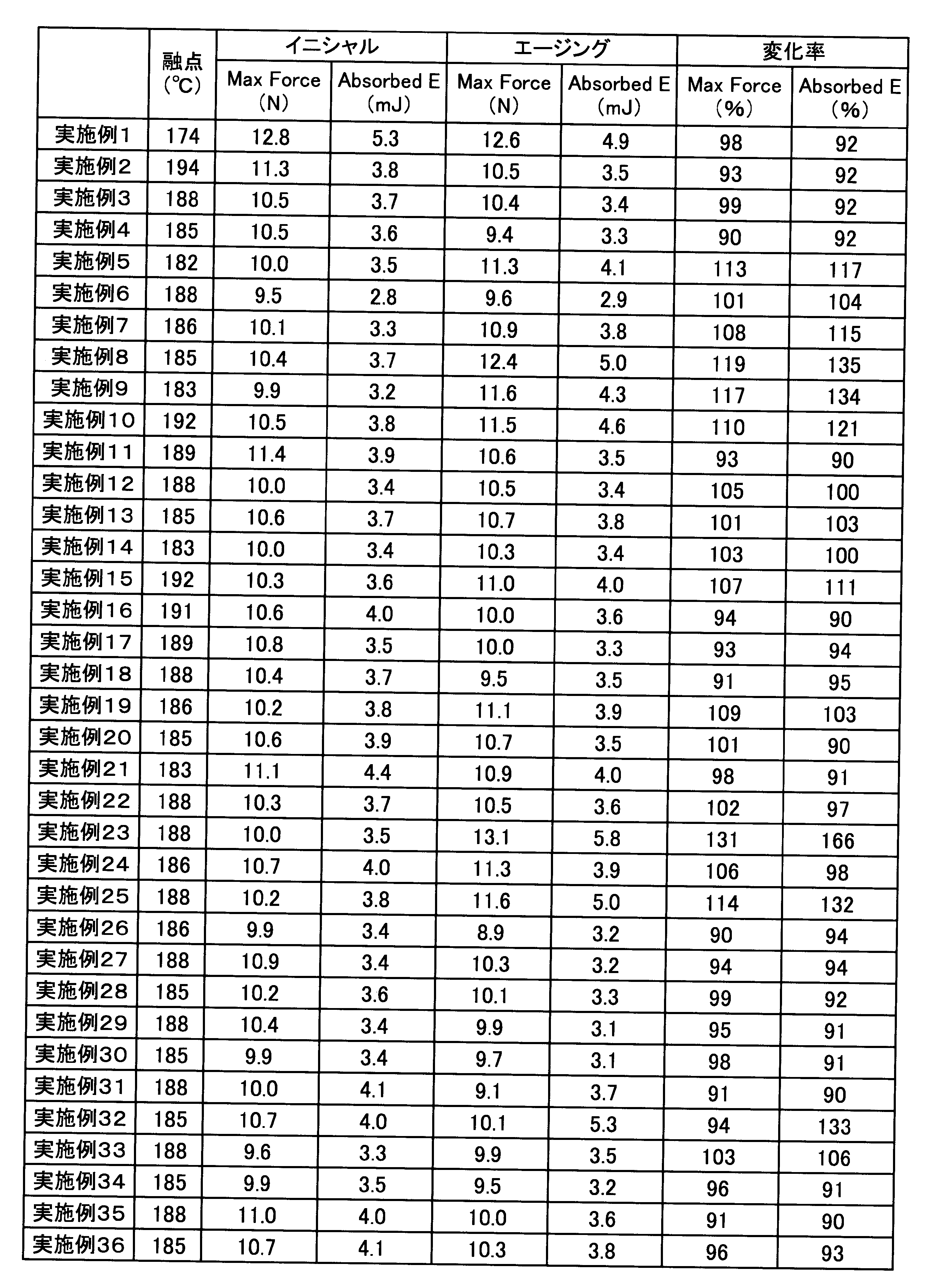
- Sn is used as the matrix phase, and Bi, Sb, Cu, and Ni are contained in a specific range to have a good shear stress, which is equivalent to or equal to the initial after aging. It can be seen that it has the above shear stress. Further, as shown in FIGS. 1 to 4, it can be seen that the generation of voids after initials and aging is suppressed. In particular, paying attention to the light gray Cu6Sn5 intermetallic compound (IMC) layer in the explanatory view of FIG. 13A, after the aging treatment of Comparative Example 4, the dark gray Cu3Sn IMC layer was formed on the surface of the black copper substrate. Many Kirkendal voids are recognized as black dots.
- IMC intermetallic compound
- the solder alloy having a specific range of component composition as described above has a low melting point based on the Bi content, is suppressed from deterioration during long-term use, and has good heat and fatigue characteristics. It is possible. Therefore, a highly reliable solder joint can be formed. Further, by containing a predetermined arbitrary element in a predetermined range in addition to the essential components of Sn, Bi, Sb, Cu and Ni, in addition to the function based on the essential component, the function peculiar to each of these arbitrary elements. Can also be demonstrated.
Landscapes
- Engineering & Computer Science (AREA)
- Mechanical Engineering (AREA)
- Chemical & Material Sciences (AREA)
- Materials Engineering (AREA)
- Metallurgy (AREA)
- Organic Chemistry (AREA)
- Electric Connection Of Electric Components To Printed Circuits (AREA)
- Connections Effected By Soldering, Adhesion, Or Permanent Deformation (AREA)
Abstract
Description
表1~3に示す組成となるように、定法に従い各金属を混合し、はんだ合金を作製した。得られたはんだ合金を用い、以下に説明する方法に従って評価試験を行った。尚、各はんだ合金は、各原料となる金属を表1~3に示す組成比になるように混合するため、原料に起因する不可避不純物を含む。


<インパクトシェア試験>
1)実施例1~36、比較例1~14で得られたはんだ合金からなる直径0.5mmの球状はんだボールを準備した。
2)銅箔基板を準備し、実装箇所に「フラックスRM-5」(日本スペリア社製)を0.01g塗布した後、はんだボールを搭載した。
3)昇温温度1.5℃/秒、最高温度200℃又は250℃で50秒間の条件でリフロー加熱し、接合させた後、冷却し、IPAにて洗浄して、フラックスを除去したものを測定用サンプルとした。
4)上記の手順で作製した測定用サンプルの一部を150℃に保持した電気炉内に100時間放置し、エージング処理を行った。
5)エージング処理を行わなかった測定用サンプル(イニシャル)、エージング処理した測定用サンプル(エージング)をインパクトシェア試験機(DAGE社製 4000HS)にセットした。
6)測定条件は、実施例1及び比較例1については10mm/秒、1000mm/秒、2000mm/秒の3種のシェア速度で実施し、実施例2~36及び比較例2~14については10mm/秒、1000mm/秒の2種のシェア速度で実施し、せん断負荷応力(N)、吸収エネルギー(Absorbed E)(mJ)を測定した。せん断負荷応力のうち、最大値(Max force)を接合強度として評価した。また、シェア速度が10mm/秒、1000mm/秒の場合について、イニシャルとエージング後の各測定値の変化率(エージング後/イニシャル×100)を算出し、エージングによる影響を評価した。測定結果を表4~8に示す。表5、7はシェア速度が10mm/秒、表6、8はシェア速度が1000mm/秒の場合の実施例1~36及び比較例1~14の結果を示したものである。また、表5~8に示した「変化率」について棒グラフとしてまとめたものを図5~8に示した。図5、7には、変化率が90%の位置に、また、図6、8には、変化率が100%の位置に、基準として波線を設けている。



実施例1、3、4及び比較例4、5で得られたはんだ合金を用い、<インパクトシェア試験>の1)~3)と同様にして測定用サンプルを作製した。測定サンプルの断面をSEMにより撮影した。得られたSEM写真のイメージ図を図1~4、9~12に示す。
ノズルに対応する薄片(純鉄製、幅10mm×長さ50mm×厚さ20μm)にフラックス(株式会社日本スペリア社製、NS-65)を塗布した後、錫メッキした。錫メッキされた薄片を試験片として以下の試験に使用した。
鉄減少率(%)=(浸漬前の面積-浸漬後の面積)/浸漬前の浸漬対象面積×100

実施例22、比較例7、11~14のはんだ合金を用いて作製したはんだ試料(直径6.5mmφ、高さ1.24mm)を用い、JIS Z 3198-3に準拠して広がり率(%)を算出し、評価した。評価基準は、広がり率が、80.0%以上を「○」、75.0%以上80.0%未満を「△」、75.0%未満を「×」とした。評価結果を表10に示す。

実施例27~36、比較例8~10、13、14のはんだ合金の溶湯はんだを鋳型に流し込み、テストピース(幅2cm×長さ10cm×厚さ1cm)を得た。酸化膜厚測定装置(ECIテクノロジー社製、Surface Scan SERA QC-100)
を用いて作製当日のテストピースの表面酸化膜厚(SnO及びSnO2の合計)を計測し、初期膜厚D0を得た後、テストピースを、室温25℃、湿度65%の環境に168時間曝し、自然酸化させた。その後、再び酸化膜厚を同様にして計測し、暴露後膜厚Dを得た。初期膜厚D0に対する変化率(D/D0×100)を算出し、評価した。評価基準は、暴露前後におけるはんだ合金表面の酸化膜厚の変化率が、25%未満を「○」、25%以上50%未満を「△」、50%以上を「×」とした。評価結果を表11に示す。

Claims (6)
- Biを32質量%以上40質量%以下、Sbを0.1質量%以上1.0質量%以下、Cuを0.1質量%以上1.0質量%以下、Niを0.001質量部以上0.1質量部以下含有し、残部がSn及び不可避不純物からなる、鉛フリーはんだ合金。
- Biを36質量%以上38質量%以下含有する、請求項1記載の鉛フリーはんだ合金。
- Agを0.3質量%以下含有する、請求項1又は2に記載の鉛フリーはんだ合金。
- Fe及びCoから選択される少なくとも1種を含有し、各含有量が0.001質量%以上0.1質量%以下である、請求項1~3の何れか1項に記載の鉛フリーはんだ合金。
- Ga、Mn、V、P及びGeから選択される少なくとも1種を含有し、各含有量が0.001質量%以上0.01質量%以下である、請求項1~4の何れか1項に記載の鉛フリーはんだ合金。
- 請求項1~5の何れか1項に記載の鉛フリーはんだ合金を用いて形成されたはんだ接合部。
Priority Applications (13)
| Application Number | Priority Date | Filing Date | Title |
|---|---|---|---|
| ES20786727T ES2938369T3 (es) | 2019-04-11 | 2020-04-10 | Aleación de soldadura sin plomo y pieza de unión por soldadura |
| KR1020217036760A KR102346712B1 (ko) | 2019-04-11 | 2020-04-10 | 무연땜납합금 및 땜납접합부 |
| BR112021020323-0A BR112021020323B1 (pt) | 2019-04-11 | 2020-04-10 | Liga de solda branca isenta de chumbo, e, parte de junta de solda branca |
| IL287143A IL287143B2 (en) | 2019-04-11 | 2020-04-10 | Lead-free solder alloy and solder joint part |
| US17/272,246 US11839937B2 (en) | 2019-04-11 | 2020-04-10 | Lead-free solder alloy and solder joint part |
| EP20786727.6A EP3828294B1 (en) | 2019-04-11 | 2020-04-10 | Lead-free solder alloy and solder joint part |
| MYPI2021004960A MY191908A (en) | 2019-04-11 | 2020-04-10 | Lead-free solder alloy and solder joint part |
| CA3136585A CA3136585C (en) | 2019-04-11 | 2020-04-10 | Lead-free solder alloy and solder joint part |
| PL20786727.6T PL3828294T3 (pl) | 2019-04-11 | 2020-04-10 | Bezołowiowy stop lutowniczy i element połączenia lutowanego |
| JP2020549069A JP6804126B1 (ja) | 2019-04-11 | 2020-04-10 | 鉛フリーはんだ合金及びはんだ接合部 |
| PH1/2021/552086A PH12021552086A1 (en) | 2019-04-11 | 2020-04-10 | Lead-free solder alloy and solder joint part |
| CN202080004183.8A CN112513300A (zh) | 2019-04-11 | 2020-04-10 | 无铅焊料合金和焊料接合部 |
| MX2021002203A MX2021002203A (es) | 2019-04-11 | 2020-04-10 | Aleacion de soldadura y pieza de union de soldadura sin plomo. |
Applications Claiming Priority (2)
| Application Number | Priority Date | Filing Date | Title |
|---|---|---|---|
| JP2019-075946 | 2019-04-11 | ||
| JP2019075946 | 2019-04-11 |
Publications (1)
| Publication Number | Publication Date |
|---|---|
| WO2020209384A1 true WO2020209384A1 (ja) | 2020-10-15 |
Family
ID=72751327
Family Applications (1)
| Application Number | Title | Priority Date | Filing Date |
|---|---|---|---|
| PCT/JP2020/016201 Ceased WO2020209384A1 (ja) | 2019-04-11 | 2020-04-10 | 鉛フリーはんだ合金及びはんだ接合部 |
Country Status (17)
| Country | Link |
|---|---|
| US (1) | US11839937B2 (ja) |
| EP (1) | EP3828294B1 (ja) |
| JP (1) | JP6804126B1 (ja) |
| KR (1) | KR102346712B1 (ja) |
| CN (2) | CN112513300A (ja) |
| BR (1) | BR112021020323B1 (ja) |
| CA (1) | CA3136585C (ja) |
| ES (1) | ES2938369T3 (ja) |
| HU (1) | HUE061181T2 (ja) |
| IL (1) | IL287143B2 (ja) |
| MX (1) | MX2021002203A (ja) |
| MY (1) | MY191908A (ja) |
| PH (1) | PH12021552086A1 (ja) |
| PL (1) | PL3828294T3 (ja) |
| PT (1) | PT3828294T (ja) |
| TW (1) | TWI819210B (ja) |
| WO (1) | WO2020209384A1 (ja) |
Cited By (3)
| Publication number | Priority date | Publication date | Assignee | Title |
|---|---|---|---|---|
| JP2022058311A (ja) * | 2020-09-30 | 2022-04-11 | 株式会社日本スペリア社 | 鉛フリーはんだ合金及びはんだ接合部 |
| WO2022234690A1 (ja) * | 2021-05-06 | 2022-11-10 | 株式会社日本スペリア社 | 鉛フリーソルダペースト |
| JP7262695B1 (ja) * | 2023-01-24 | 2023-04-21 | 株式会社タムラ製作所 | はんだ合金、接合部、接合材、ソルダペースト、接合構造体および電子制御装置 |
Families Citing this family (3)
| Publication number | Priority date | Publication date | Assignee | Title |
|---|---|---|---|---|
| JP7161140B1 (ja) * | 2022-07-22 | 2022-10-26 | 千住金属工業株式会社 | はんだ合金、はんだボール、はんだペーストおよびはんだ継手 |
| WO2024042663A1 (ja) | 2022-08-24 | 2024-02-29 | 株式会社タムラ製作所 | はんだ合金、接合部、接合材、ソルダペースト、接合構造体および電子制御装置 |
| CN115383349B (zh) * | 2022-10-09 | 2023-11-07 | 云南锡业集团(控股)有限责任公司研发中心 | 微合金化调控微观结构获得高韧性无铅锡铋焊料的方法 |
Citations (6)
| Publication number | Priority date | Publication date | Assignee | Title |
|---|---|---|---|---|
| JPH0740079A (ja) | 1993-07-28 | 1995-02-10 | Nippon Superiashiya:Kk | 無鉛はんだ合金 |
| JP2007090407A (ja) | 2005-09-30 | 2007-04-12 | Toshiba Corp | 電子部品の接合材料、プリント回路配線基板、及び電子機器 |
| JP2014140865A (ja) | 2013-01-23 | 2014-08-07 | Hitachi Metals Ltd | 無鉛はんだ |
| WO2015019966A1 (ja) * | 2013-08-05 | 2015-02-12 | 千住金属工業株式会社 | 鉛フリーはんだ合金 |
| WO2018028080A1 (zh) * | 2016-08-11 | 2018-02-15 | 北京康普锡威科技有限公司 | 一种SnBiSb系低温无铅焊料及其制备方法 |
| JP2018121055A (ja) * | 2017-01-20 | 2018-08-02 | レノボ・シンガポール・プライベート・リミテッド | はんだ接合方法、およびはんだ継手 |
Family Cites Families (13)
| Publication number | Priority date | Publication date | Assignee | Title |
|---|---|---|---|---|
| US6156132A (en) | 1998-02-05 | 2000-12-05 | Fuji Electric Co., Ltd. | Solder alloys |
| CN1919522A (zh) * | 2005-09-23 | 2007-02-28 | 东莞市千岛金属锡品有限公司 | 一种环保型高温抗氧化焊料 |
| CN102029479A (zh) * | 2010-12-29 | 2011-04-27 | 广州有色金属研究院 | 一种低银无铅焊料合金及其制备方法和装置 |
| US20160074971A1 (en) * | 2013-04-18 | 2016-03-17 | Senju Metal Industry Co., Ltd. | Lead-Free Solder Alloy |
| JP6111952B2 (ja) * | 2013-09-25 | 2017-04-12 | 日立金属株式会社 | 無鉛はんだ合金、接合材及び接合体 |
| EP3138658B1 (en) * | 2014-04-30 | 2020-11-04 | Nihon Superior Co., Ltd. | Lead-free solder alloy |
| WO2016178000A1 (en) * | 2015-05-02 | 2016-11-10 | Alpha Metals, Inc. | Lead-free solder alloy with low melting point |
| CN105195915B (zh) * | 2015-10-30 | 2017-05-24 | 苏州优诺电子材料科技有限公司 | 一种低温无铅焊料合金 |
| CN105215569A (zh) * | 2015-10-30 | 2016-01-06 | 苏州优诺电子材料科技有限公司 | 一种无铅焊料合金 |
| JP7216419B2 (ja) * | 2017-03-31 | 2023-02-01 | 株式会社日本スペリア社 | 鉛フリーはんだ合金及びはんだ継手 |
| JP6477965B1 (ja) * | 2018-03-08 | 2019-03-06 | 千住金属工業株式会社 | はんだ合金、はんだペースト、はんだボール、やに入りはんだおよびはんだ継手 |
| CN112638574A (zh) * | 2018-08-31 | 2021-04-09 | 铟泰公司 | SnBi和SnIn焊锡合金 |
| CN109158795B (zh) * | 2018-10-12 | 2021-08-06 | 苏州优诺电子材料科技有限公司 | 一种低温焊料合金粉及其制备方法 |
-
2020
- 2020-04-10 JP JP2020549069A patent/JP6804126B1/ja active Active
- 2020-04-10 PH PH1/2021/552086A patent/PH12021552086A1/en unknown
- 2020-04-10 CN CN202080004183.8A patent/CN112513300A/zh active Pending
- 2020-04-10 IL IL287143A patent/IL287143B2/en unknown
- 2020-04-10 PT PT207867276T patent/PT3828294T/pt unknown
- 2020-04-10 MY MYPI2021004960A patent/MY191908A/en unknown
- 2020-04-10 BR BR112021020323-0A patent/BR112021020323B1/pt active IP Right Grant
- 2020-04-10 EP EP20786727.6A patent/EP3828294B1/en active Active
- 2020-04-10 US US17/272,246 patent/US11839937B2/en active Active
- 2020-04-10 ES ES20786727T patent/ES2938369T3/es active Active
- 2020-04-10 KR KR1020217036760A patent/KR102346712B1/ko active Active
- 2020-04-10 TW TW109112255A patent/TWI819210B/zh active
- 2020-04-10 PL PL20786727.6T patent/PL3828294T3/pl unknown
- 2020-04-10 HU HUE20786727A patent/HUE061181T2/hu unknown
- 2020-04-10 CN CN202111287526.9A patent/CN113897511A/zh active Pending
- 2020-04-10 MX MX2021002203A patent/MX2021002203A/es unknown
- 2020-04-10 WO PCT/JP2020/016201 patent/WO2020209384A1/ja not_active Ceased
- 2020-04-10 CA CA3136585A patent/CA3136585C/en active Active
Patent Citations (7)
| Publication number | Priority date | Publication date | Assignee | Title |
|---|---|---|---|---|
| JPH0740079A (ja) | 1993-07-28 | 1995-02-10 | Nippon Superiashiya:Kk | 無鉛はんだ合金 |
| JP2007090407A (ja) | 2005-09-30 | 2007-04-12 | Toshiba Corp | 電子部品の接合材料、プリント回路配線基板、及び電子機器 |
| JP2014140865A (ja) | 2013-01-23 | 2014-08-07 | Hitachi Metals Ltd | 無鉛はんだ |
| WO2015019966A1 (ja) * | 2013-08-05 | 2015-02-12 | 千住金属工業株式会社 | 鉛フリーはんだ合金 |
| JP5679094B1 (ja) | 2013-08-05 | 2015-03-04 | 千住金属工業株式会社 | 鉛フリーはんだ合金 |
| WO2018028080A1 (zh) * | 2016-08-11 | 2018-02-15 | 北京康普锡威科技有限公司 | 一种SnBiSb系低温无铅焊料及其制备方法 |
| JP2018121055A (ja) * | 2017-01-20 | 2018-08-02 | レノボ・シンガポール・プライベート・リミテッド | はんだ接合方法、およびはんだ継手 |
Non-Patent Citations (1)
| Title |
|---|
| See also references of EP3828294A4 |
Cited By (6)
| Publication number | Priority date | Publication date | Assignee | Title |
|---|---|---|---|---|
| JP2022058311A (ja) * | 2020-09-30 | 2022-04-11 | 株式会社日本スペリア社 | 鉛フリーはんだ合金及びはんだ接合部 |
| JP7835370B2 (ja) | 2020-09-30 | 2026-03-25 | 株式会社日本スペリア社 | 鉛フリーはんだ合金及びはんだ接合部 |
| WO2022234690A1 (ja) * | 2021-05-06 | 2022-11-10 | 株式会社日本スペリア社 | 鉛フリーソルダペースト |
| JPWO2022234690A1 (ja) * | 2021-05-06 | 2022-11-10 | ||
| JP7262695B1 (ja) * | 2023-01-24 | 2023-04-21 | 株式会社タムラ製作所 | はんだ合金、接合部、接合材、ソルダペースト、接合構造体および電子制御装置 |
| WO2024157366A1 (ja) * | 2023-01-24 | 2024-08-02 | 株式会社タムラ製作所 | はんだ合金、接合部、接合材、ソルダペースト、接合構造体および電子制御装置 |
Also Published As
| Publication number | Publication date |
|---|---|
| PL3828294T3 (pl) | 2023-03-13 |
| KR102346712B1 (ko) | 2021-12-31 |
| EP3828294A4 (en) | 2021-07-07 |
| IL287143B1 (en) | 2024-08-01 |
| MY191908A (en) | 2022-07-18 |
| CN112513300A (zh) | 2021-03-16 |
| PT3828294T (pt) | 2023-01-26 |
| IL287143B2 (en) | 2024-12-01 |
| HUE061181T2 (hu) | 2023-05-28 |
| JP6804126B1 (ja) | 2020-12-23 |
| US20220016733A1 (en) | 2022-01-20 |
| JPWO2020209384A1 (ja) | 2021-04-30 |
| EP3828294A1 (en) | 2021-06-02 |
| EP3828294B1 (en) | 2022-11-16 |
| BR112021020323B1 (pt) | 2022-08-30 |
| CA3136585A1 (en) | 2020-10-15 |
| US11839937B2 (en) | 2023-12-12 |
| CN113897511A (zh) | 2022-01-07 |
| PH12021552086A1 (en) | 2022-05-23 |
| KR20210149831A (ko) | 2021-12-09 |
| TWI819210B (zh) | 2023-10-21 |
| TW202045291A (zh) | 2020-12-16 |
| MX2021002203A (es) | 2021-05-14 |
| IL287143A (en) | 2021-12-01 |
| CA3136585C (en) | 2022-09-13 |
| BR112021020323A2 (ja) | 2021-12-14 |
| ES2938369T3 (es) | 2023-04-10 |
Similar Documents
| Publication | Publication Date | Title |
|---|---|---|
| JP6804126B1 (ja) | 鉛フリーはんだ合金及びはんだ接合部 | |
| AU757312B2 (en) | Leadless solder | |
| WO2012128356A1 (ja) | 鉛フリーはんだ合金 | |
| WO2019094242A1 (en) | Low-silver tin based alternative solder alloy to standard sac alloys for high reliability applications | |
| JP5973992B2 (ja) | はんだ合金 | |
| JP4453473B2 (ja) | 鉛フリーはんだ合金と、それを用いたはんだ材料及びはんだ接合部 | |
| TWI821211B (zh) | 用於電子應用之成本效益高的無鉛焊料合金 | |
| CN1168571C (zh) | 无铅软钎焊料合金 | |
| EP3707286A1 (en) | High reliability lead-free solder alloy for electronic applications in extreme environments | |
| JP3758090B2 (ja) | SnCu系無鉛はんだ合金 | |
| JP2022058311A (ja) | 鉛フリーはんだ合金及びはんだ接合部 |
Legal Events
| Date | Code | Title | Description |
|---|---|---|---|
| ENP | Entry into the national phase |
Ref document number: 2020549069 Country of ref document: JP Kind code of ref document: A |
|
| 121 | Ep: the epo has been informed by wipo that ep was designated in this application |
Ref document number: 20786727 Country of ref document: EP Kind code of ref document: A1 |
|
| WWE | Wipo information: entry into national phase |
Ref document number: MX/A/2021/002203 Country of ref document: MX |
|
| ENP | Entry into the national phase |
Ref document number: 2020786727 Country of ref document: EP Effective date: 20210226 |
|
| WWP | Wipo information: published in national office |
Ref document number: MX/A/2021/002203 Country of ref document: MX |
|
| ENP | Entry into the national phase |
Ref document number: 3136585 Country of ref document: CA |
|
| NENP | Non-entry into the national phase |
Ref country code: DE |
|
| REG | Reference to national code |
Ref country code: BR Ref legal event code: B01A Ref document number: 112021020323 Country of ref document: BR |
|
| ENP | Entry into the national phase |
Ref document number: 20217036760 Country of ref document: KR Kind code of ref document: A |
|
| ENP | Entry into the national phase |
Ref document number: 112021020323 Country of ref document: BR Kind code of ref document: A2 Effective date: 20211008 |
|
| WWG | Wipo information: grant in national office |
Ref document number: MX/A/2021/002203 Country of ref document: MX |