WO2020226031A1 - 光デバイスおよび光検出システム - Google Patents
光デバイスおよび光検出システム Download PDFInfo
- Publication number
- WO2020226031A1 WO2020226031A1 PCT/JP2020/016394 JP2020016394W WO2020226031A1 WO 2020226031 A1 WO2020226031 A1 WO 2020226031A1 JP 2020016394 W JP2020016394 W JP 2020016394W WO 2020226031 A1 WO2020226031 A1 WO 2020226031A1
- Authority
- WO
- WIPO (PCT)
- Prior art keywords
- light
- mirror
- optical
- wavelength
- waveguide
- Prior art date
- Legal status (The legal status is an assumption and is not a legal conclusion. Google has not performed a legal analysis and makes no representation as to the accuracy of the status listed.)
- Ceased
Links
Images








Classifications
-
- G—PHYSICS
- G02—OPTICS
- G02B—OPTICAL ELEMENTS, SYSTEMS OR APPARATUS
- G02B6/00—Light guides; Structural details of arrangements comprising light guides and other optical elements, e.g. couplings
- G02B6/10—Light guides; Structural details of arrangements comprising light guides and other optical elements, e.g. couplings of the optical waveguide type
- G02B6/12—Light guides; Structural details of arrangements comprising light guides and other optical elements, e.g. couplings of the optical waveguide type of the integrated circuit kind
- G02B6/122—Basic optical elements, e.g. light-guiding paths
- G02B6/124—Geodesic lenses or integrated gratings
-
- G—PHYSICS
- G01—MEASURING; TESTING
- G01S—RADIO DIRECTION-FINDING; RADIO NAVIGATION; DETERMINING DISTANCE OR VELOCITY BY USE OF RADIO WAVES; LOCATING OR PRESENCE-DETECTING BY USE OF THE REFLECTION OR RERADIATION OF RADIO WAVES; ANALOGOUS ARRANGEMENTS USING OTHER WAVES
- G01S7/00—Details of systems according to groups G01S13/00, G01S15/00, G01S17/00
- G01S7/48—Details of systems according to groups G01S13/00, G01S15/00, G01S17/00 of systems according to group G01S17/00
- G01S7/481—Constructional features, e.g. arrangements of optical elements
- G01S7/4817—Constructional features, e.g. arrangements of optical elements relating to scanning
-
- G—PHYSICS
- G01—MEASURING; TESTING
- G01S—RADIO DIRECTION-FINDING; RADIO NAVIGATION; DETERMINING DISTANCE OR VELOCITY BY USE OF RADIO WAVES; LOCATING OR PRESENCE-DETECTING BY USE OF THE REFLECTION OR RERADIATION OF RADIO WAVES; ANALOGOUS ARRANGEMENTS USING OTHER WAVES
- G01S7/00—Details of systems according to groups G01S13/00, G01S15/00, G01S17/00
- G01S7/48—Details of systems according to groups G01S13/00, G01S15/00, G01S17/00 of systems according to group G01S17/00
- G01S7/481—Constructional features, e.g. arrangements of optical elements
- G01S7/4818—Constructional features, e.g. arrangements of optical elements using optical fibres
-
- G—PHYSICS
- G02—OPTICS
- G02F—OPTICAL DEVICES OR ARRANGEMENTS FOR THE CONTROL OF LIGHT BY MODIFICATION OF THE OPTICAL PROPERTIES OF THE MEDIA OF THE ELEMENTS INVOLVED THEREIN; NON-LINEAR OPTICS; FREQUENCY-CHANGING OF LIGHT; OPTICAL LOGIC ELEMENTS; OPTICAL ANALOGUE/DIGITAL CONVERTERS
- G02F1/00—Devices or arrangements for the control of the intensity, colour, phase, polarisation or direction of light arriving from an independent light source, e.g. switching, gating or modulating; Non-linear optics
- G02F1/29—Devices or arrangements for the control of the intensity, colour, phase, polarisation or direction of light arriving from an independent light source, e.g. switching, gating or modulating; Non-linear optics for the control of the position or the direction of light beams, i.e. deflection
- G02F1/295—Analog deflection from or in an optical waveguide structure]
-
- G—PHYSICS
- G01—MEASURING; TESTING
- G01S—RADIO DIRECTION-FINDING; RADIO NAVIGATION; DETERMINING DISTANCE OR VELOCITY BY USE OF RADIO WAVES; LOCATING OR PRESENCE-DETECTING BY USE OF THE REFLECTION OR RERADIATION OF RADIO WAVES; ANALOGOUS ARRANGEMENTS USING OTHER WAVES
- G01S17/00—Systems using the reflection or reradiation of electromagnetic waves other than radio waves, e.g. lidar systems
- G01S17/88—Lidar systems specially adapted for specific applications
- G01S17/93—Lidar systems specially adapted for specific applications for anti-collision purposes
Definitions
- This disclosure relates to optical devices and photodetection systems.
- Patent Document 1 discloses a configuration in which scanning by light can be performed by using a driving device that rotates a mirror.
- Patent Document 2 discloses an optical phased array having a plurality of nanophotonic antenna elements arranged two-dimensionally. Each antenna element is optically coupled to a variable light delay line (ie, phase shifter). In this optical phased array, a coherent optical beam is guided to each antenna element by a waveguide, and the phase shifter shifts the phase of the optical beam. As a result, the amplitude distribution of the far-field radiation pattern can be changed.
- a variable light delay line ie, phase shifter
- Patent Document 3 describes a waveguide provided with an optical waveguide layer in which light is waveguideed inside and first-distributed Bragg reflectors formed on the upper and lower surfaces of the optical waveguide layer, and a waveguide for causing light to enter the waveguide.
- a light deflecting element including a light incident port and a light emitting port formed on the surface of the waveguide for emitting light incident from the light incident port and waveguide in the waveguide is disclosed.
- One aspect of the present disclosure provides a novel optical device capable of realizing scanning by light with a relatively simple configuration.
- the optical device has a first reflective surface, a first mirror extending along a first direction, and a second reflective surface facing the first reflective surface.
- a second mirror extending along the first direction and an optical waveguide layer located between the first mirror and the second mirror and propagating light along the first direction.
- the transmittance of the first mirror is higher than the transmittance of the second mirror, and the light is incident from the normal direction of the reflecting surface of at least one of the first mirror and the second mirror.
- the reflection spectrum with respect to the light includes a maximum point in a wavelength region where the transmittance is 90% or more, and first and second bending points on the long wavelength side of the maximum point.
- a one-dimensional scan or a two-dimensional scan using light can be realized with a relatively simple configuration.
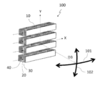
- FIG. 1 is a perspective view schematically showing an example of an optical scanning device.
- FIG. 2 is a diagram schematically showing an example of a cross-sectional structure of one waveguide element and propagating light.
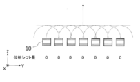
- FIG. 3A is a diagram showing a cross section of a waveguide array that emits light in a direction perpendicular to the exit surface of the waveguide array.
- FIG. 3B is a diagram showing a cross section of a waveguide array that emits light in a direction different from the direction perpendicular to the exit surface of the waveguide array.
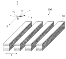
- FIG. 4 is a perspective view schematically showing an example of a waveguide array in a three-dimensional space.
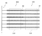
- FIG. 5 is a schematic view of the waveguide array and the phase shifter array as viewed from the normal direction (Z direction) of the light emitting surface.
- FIG. 6A is a diagram schematically showing how light is emitted from the emission surface when the propagation angle is small.
- FIG. 6B is a diagram schematically showing how light is emitted from the emission surface when the propagation angle is large.
- FIG. 7 is a diagram showing the result of calculating the relationship between the propagation length and the beam line width of the emitted light.
- FIG. 8 is a diagram showing a reflection spectrum of a conventional DBR with respect to an incident angle of 0 °.
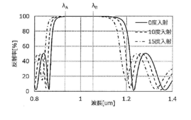
- FIG. 9 is a diagram showing the reflection spectra of a conventional DBR for incident angles of 0 °, 10 °, and 15 °.
- FIG. 10A is a diagram showing an example of the relationship between the incident angle and the reflectance at a wavelength of 940 nm.
- FIG. 10B is a diagram showing an example of the relationship between the incident angle and the reflectance at a wavelength of 1100 nm.
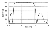
- FIG. 11 is a diagram showing a reflection spectrum of the chirp DBR of the present embodiment with respect to an incident angle of 0 °.
- FIG. 12 is a diagram showing an example of the relationship between the incident angle and the reflectance at a wavelength of 940 nm.
- FIG. 13 is a diagram showing an example of the relationship between the emission angle and the propagation length.
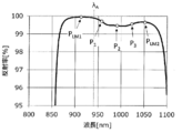
- FIG. 14 is a diagram showing a reflection spectrum of another chirp DBR of the present embodiment with respect to an incident angle of 0 °.
- FIG. 15 is a diagram showing a configuration example of an optical scanning device in which elements such as an optical turnout, a waveguide array, a phase shifter array, and a light source are integrated on a circuit board.
- FIG. 16 is a schematic view showing a state in which a two-dimensional scan is performed by irradiating a light beam such as a laser far from the light scanning device.
- FIG. 17 is a block diagram showing a configuration example of a LiDAR system capable of generating a ranging image.
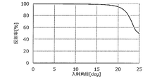
- FIG. 18 is a diagram showing an example of the relationship between the incident angle ⁇ and the reflectance at a propagation length of 100 ⁇ m.
- the present inventor has found that a conventional optical scanning device has a problem that it is difficult to scan a space with light without complicating the configuration of the device.
- the present inventor paid attention to the above-mentioned problems in the prior art, and examined the configuration for solving these problems.
- the present inventor has found that the above problems can be solved by using a waveguide element having a pair of mirrors facing each other and an optical waveguide layer sandwiched between the mirrors.
- One of the pair of mirrors in the waveguide element has a higher light transmittance than the other, and emits a part of the light propagating in the optical waveguide layer to the outside.
- the direction (or exit angle) of the emitted light can be changed by adjusting the refractive index or thickness of the optical waveguide layer or the wavelength of the light input to the optical waveguide layer, as will be described later. More specifically, by changing the refractive index, thickness, or wavelength, the component of the wave vector of the emitted light in the direction along the longitudinal direction of the optical waveguide layer can be changed. As a result, a one-dimensional scan is realized.
- a two-dimensional scan can be realized. More specifically, by giving an appropriate phase difference to the light supplied to the plurality of waveguide elements and adjusting the phase difference, it is possible to change the direction in which the light emitted from the plurality of waveguide elements strengthens each other. it can. Due to the change in the phase difference, the component of the wave vector of the emitted light in the direction intersecting the longitudinal direction of the optical waveguide layer changes. This makes it possible to realize a two-dimensional scan. Even when performing a two-dimensional scan, it is not necessary to change the refractive index, thickness, or wavelength of light of the plurality of optical waveguide layers by different amounts.
- Two-dimensional scanning can be performed.
- one-dimensional or two-dimensional scanning by light can be realized with a relatively simple configuration.
- the refractive index, the thickness, and the wavelength is selected from the group consisting of the refractive index of the optical waveguide layer, the thickness of the optical waveguide layer, and the wavelength input to the optical waveguide layer. Means at least one to be done. Any one of the refractive index, the thickness, and the wavelength may be controlled independently in order to change the emission direction of the light. Alternatively, any two or all of these three may be controlled to change the light emission direction. Instead of or in addition to controlling the index of refraction or thickness, the wavelength of light input to the optical waveguide layer may be controlled.
- the above basic principle can be applied not only to applications that emit light but also to applications that receive optical signals.
- the direction of the light that can be received can be changed one-dimensionally.
- the phase difference of light is changed by a plurality of phase shifters connected to a plurality of waveguide elements arranged in one direction, the direction of receivable light can be changed two-dimensionally.
- the optical scanning device and the optical receiving device of the present disclosure can be used as an antenna in an optical detection system such as a LiDAR (Light Detection and Ringing) system, for example.
- a LiDAR Light Detection and Ringing
- the LiDAR system uses short wavelength electromagnetic waves (visible light, infrared rays, or ultraviolet rays) as compared with a radar system using radio waves such as millimeter waves, it is possible to detect the distance distribution of an object with high resolution.
- a LiDAR system can be mounted on a moving body such as an automobile, a UAV (Unmanned Aerial Vehicle, so-called drone), or an AGV (Automated Guided Vehicle), and can be used as one of collision avoidance technologies.
- UAV Unmanned Aerial Vehicle, so-called drone
- AGV Automatic Guided Vehicle
- optical scanning device and the optical receiving device may be collectively referred to as "optical device”.
- a device used for an optical scanning device or an optical receiving device may also be referred to as an “optical device”.
- optical device is also used for the optical components that make up an optical scanning device or optical receiving device.
- light refers to electromagnetic waves including not only visible light (wavelength of about 400 nm to about 700 nm) but also ultraviolet rays (wavelength of about 10 nm to about 400 nm) and infrared rays (wavelength of about 700 nm to about 1 mm). means.
- ultraviolet rays may be referred to as “ultraviolet light” and infrared rays may be referred to as “infrared light”.
- scanning by light means changing the direction of light.
- One-dimensional scanning means changing the direction of light linearly along a direction that intersects that direction.
- Tele-dimensional scanning means changing the direction of light two-dimensionally along a plane that intersects the direction.
- FIG. 1 is a perspective view schematically showing an example of the optical scanning device 100.
- the optical scanning device 100 includes a waveguide array including a plurality of waveguide elements 10.
- Each of the plurality of waveguide elements 10 has a shape extending in the first direction (X direction in FIG. 1).
- the plurality of waveguide elements 10 are regularly arranged in a second direction (Y direction in FIG. 1) intersecting the first direction.
- the plurality of waveguide elements 10 propagate the light in the first direction and emit the light in the third direction D3 which intersects the virtual plane parallel to the first and second directions.
- the first direction (X direction) and the second direction (Y direction) are orthogonal to each other, but both may not be orthogonal to each other.
- a plurality of waveguide elements 10 are arranged at equal intervals in the Y direction, but they do not necessarily have to be arranged at equal intervals.
- Each of the plurality of waveguide elements 10 is located between the first mirror 30 and the second mirror 40 (hereinafter, each of which may be simply referred to as a "mirror") facing each other and the mirror 30 and the mirror 40. It has an optical waveguide layer 20 to be used. Each of the mirror 30 and the mirror 40 has a reflective surface intersecting the third direction D3 at the interface with the optical waveguide layer 20. The mirror 30, the mirror 40, and the optical waveguide layer 20 have a shape extending in the first direction (X direction).
- the reflecting surface of the first mirror 30 and the reflecting surface of the second mirror 40 face each other substantially in parallel.
- the first mirror 30 has a property of transmitting a part of the light propagating in the optical waveguide layer 20.
- the first mirror 30 has a higher light transmittance than the second mirror 40 for the light. Therefore, a part of the light propagating in the optical waveguide layer 20 is emitted to the outside from the first mirror 30.
- Such mirrors 30 and 40 are, for example, multilayer mirrors formed by a multilayer film made of a dielectric (sometimes referred to as a "multilayer reflector” or a "Distributed Bragg Reflector (DBR)"). possible.
- the phase of the light input to each waveguide element 10 is controlled, and the refractive index or thickness of the optical waveguide layer 20 in these waveguide elements 10 or the wavelength of the light input to the optical waveguide layer 20 is synchronized. By changing at the same time, a two-dimensional scan using light can be realized.
- the present inventor analyzed the operating principle of the waveguide element 10 in order to realize such a two-dimensional scan. Based on the result, we succeeded in realizing a two-dimensional scan by light by driving a plurality of waveguide elements 10 in synchronization.
- each waveguide element 10 when light is input to each waveguide element 10, light is emitted from the emission surface of each waveguide element 10.
- the exit surface is located on the opposite side of the reflection surface of the first mirror 30.
- the direction D3 of the emitted light depends on the refractive index, the thickness, and the wavelength of the light of the optical waveguide layer.
- at least one of the refractive index, thickness, and wavelength of each optical waveguide layer is synchronously controlled so that the light emitted from each waveguide element 10 is in substantially the same direction.
- the X-direction component of the wave number vector of the light emitted from the plurality of waveguide elements 10 can be changed.
- the direction D3 of the emitted light can be changed along the direction 101 shown in FIG.
- the emitted light interferes with each other.
- the direction in which the light intensifies due to interference can be changed. For example, when a plurality of waveguide elements 10 having the same size are arranged at equal intervals in the Y direction, light having a different phase is input to the plurality of waveguide elements 10 by a fixed amount. By changing the phase difference, the component in the Y direction of the wave number vector of the emitted light can be changed.
- the direction D3 in which the emitted light is strengthened by interference can be changed along the direction 102 shown in FIG. ..
- a two-dimensional scan using light can be realized.
- optical scanning device 100 The operating principle of the optical scanning device 100 will be described below.
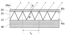
- FIG. 2 is a diagram schematically showing an example of a cross-sectional structure of one waveguide element 10 and propagating light.
- the X direction and the direction perpendicular to the Y direction shown in FIG. 1 are defined as the Z direction, and a cross section parallel to the XZ plane of the waveguide element 10 is schematically shown.
- a pair of mirrors 30 and mirrors 40 are arranged so as to sandwich the optical waveguide layer 20.
- the light 22 introduced from one end of the optical waveguide layer 20 in the X direction is the first reflecting surface 30s and the lower surface (lower surface) of the first mirror 30 provided on the upper surface (upper surface in FIG. 2) of the optical waveguide layer 20.
- the light transmittance of the first mirror 30 is higher than the light transmittance of the second mirror 40. Therefore, a part of the light can be mainly output from the exit surface 30es of the first mirror 30.
- the first reflecting surface 30s may be simply referred to as a “reflecting surface 30s”
- the second reflecting surface 40s may be simply referred to as a “reflecting surface 40s”.
- the light propagation angle means the angle of incidence on the interface between the mirror 30 or the mirror 40 and the optical waveguide layer 20.
- Light that is incident at an angle closer to perpendicular to the mirror 30 or 40 can also propagate. That is, light incident on the interface can be propagated at an angle smaller than the critical angle of total reflection. Therefore, the group velocity of light in the propagation direction of light is significantly lower than the speed of light in free space.
- the waveguide element 10 has the property that the light propagation conditions change significantly with respect to changes in the wavelength of light, the thickness of the optical waveguide layer 20, and the refractive index of the optical waveguide layer 20.
- the waveguide element 10 is also referred to as a "reflective waveguide” or a “slow light waveguide”.
- the emission angle ⁇ of the light emitted from the waveguide element 10 into the air is expressed by the following equation (1).
- the light emission direction is changed by changing any of the wavelength ⁇ of the light in the air, the refractive index n w of the optical waveguide layer 20, and the thickness d of the optical waveguide layer 20. Can be done.
- the optical scanning device 100 of the present disclosure at least one of the wavelength ⁇ of the light input to the optical waveguide layer 20, the refractive index n w of the optical waveguide layer 20, and the thickness d of the optical waveguide layer 20 is controlled. Thereby, the emission direction of the light is controlled.
- the wavelength ⁇ of light may remain constant during operation without change. In that case, light scanning can be realized with a simpler configuration.
- the wavelength ⁇ is not particularly limited.
- the wavelength ⁇ is in the wavelength range of 400 nm to 1100 nm (visible light to near infrared light), which provides high detection sensitivity with a photodetector or image sensor that detects light by absorbing light with general silicon (Si). Can be included in.
- the wavelength ⁇ may be included in the near infrared light wavelength range of 1260 nm to 1625 nm, which has a relatively low transmission loss in an optical fiber or Si waveguide. These wavelength ranges are examples.
- the wavelength range of the light used is not limited to the wavelength range of visible light or infrared light, and may be, for example, the wavelength range of ultraviolet light.
- the optical scanning device 100 may include a first adjusting element that changes at least one of the refractive index, thickness, and wavelength of the optical waveguide layer 20 in each waveguide element 10.
- the light emission direction can be significantly changed by changing at least one of the refractive index n w, the thickness d, and the wavelength ⁇ of the optical waveguide layer 20. ..
- the emission angle of the light emitted from the mirror 30 can be changed in the direction along the waveguide element 10.
- Such a one-dimensional scan can be realized by using at least one waveguide element 10.
- the optical waveguide layer 20 may include a liquid crystal material or an electro-optical material.
- the optical waveguide layer 20 may be sandwiched by a pair of electrodes. By applying a voltage to the pair of electrodes, the refractive index of the optical waveguide layer 20 can be changed.
- At least one actuator may be connected to at least one of the first mirror 30 and the second mirror 40.
- the thickness of the optical waveguide layer 20 can be changed by changing the distance between the first mirror 30 and the second mirror 40 by at least one actuator. If the optical waveguide layer 20 is formed of a liquid, the thickness of the optical waveguide layer 20 can easily change.
- FIG. 3A is a diagram showing a cross section of a waveguide array that emits light in a direction perpendicular to the exit surface of the waveguide array.
- FIG. 3A also shows the amount of phase shift of the light propagating through each waveguide element 10.
- the phase shift amount is a value based on the phase of the light propagating through the waveguide element 10 at the left end.
- the waveguide array of the present disclosure includes a plurality of waveguide elements 10 arranged at equal intervals.
- the broken line arc indicates the wave plane of the light emitted from each waveguide element 10.
- the straight line shows the wave surface formed by the interference of light.
- the arrows indicate the direction of the light emitted from the waveguide array (ie, the direction of the wave vector).
- the phases of the light propagating in the optical waveguide layer 20 in each waveguide element 10 are the same.
- the light is emitted in a direction (Z direction) perpendicular to both the arrangement direction (Y direction) of the waveguide element 10 and the direction (X direction) in which the optical waveguide layer 20 extends.
- FIG. 3B is a diagram showing a cross section of a waveguide array that emits light in a direction different from the direction perpendicular to the exit surface of the waveguide array.
- the phases of the light propagating in the optical waveguide layer 20 in the plurality of waveguide elements 10 are different by a fixed amount ( ⁇ ) in the arrangement direction.
- the light is emitted in a direction different from the Z direction.
- ⁇ the component in the Y direction of the wave number vector of light can be changed.
- the light emission angle ⁇ 0 is expressed by the following equation (2).
- the direction of the light emitted from the optical scanning device 100 is not parallel to the XZ plane or the YZ plane. That is, ⁇ ⁇ 0 ° and ⁇ 0 ⁇ 0 °.
- FIG. 4 is a perspective view schematically showing an example of a waveguide array in a three-dimensional space.
- the thick arrow shown in FIG. 4 indicates the direction of the light emitted from the optical scanning device 100.
- ⁇ is the angle formed by the light emission direction and the YZ plane.
- ⁇ satisfies equation (1).
- ⁇ 0 is the angle formed by the light emission direction and the XZ plane.
- ⁇ 0 satisfies equation (2).
- phase shifter for changing the phase of the light may be provided before introducing the light into the waveguide element 10.
- the optical scan device 100 of the present disclosure includes a plurality of phase shifters connected to each of the plurality of waveguide elements 10 and a second adjusting element for adjusting the phase of light propagating through each phase shifter.
- Each phase shifter includes a waveguide that is directly connected to the optical waveguide layer 20 in one of the plurality of waveguide elements 10 or via another waveguide.
- the second adjusting element changes the phase difference of the light propagating from the plurality of phase shifters to the plurality of waveguide elements 10, so that the direction of the light emitted from the plurality of waveguide elements 10 (that is, the third).
- the direction D3) of is changed.
- a plurality of arranged phase shifters may be referred to as a "phase shifter array" as in the waveguide array.
- FIG. 5 is a schematic view of the waveguide array 10A and the phase shifter array 80A as viewed from the normal direction (Z direction) of the light emitting surface.
- all phase shifters 80 have the same propagation characteristics, and all waveguide elements 10 have the same propagation characteristics.
- Each phase shifter 80 and each waveguide element 10 may have the same length or may have different lengths.
- the respective phase shift amounts can be adjusted by the drive voltage. Further, by adopting a structure in which the length of each phase shifter 80 is changed in equal steps, it is possible to give the phase shift in equal steps with the same drive voltage.
- the optical scan device 100 drives an optical turnout 90 that branches and supplies light to a plurality of phase shifters 80, a first drive circuit 110 that drives each waveguide element 10, and each phase shifter 80.
- a second drive circuit 210 is further provided.
- the straight arrow shown in FIG. 5 represents the input of light.
- Two-dimensional scanning can be realized by independently controlling the first drive circuit 110 and the second drive circuit 210, which are provided separately.
- the first drive circuit 110 functions as one element of the first adjustment element
- the second drive circuit 210 functions as one element of the second adjustment element.
- the first drive circuit 110 changes the angle of light emitted from the optical waveguide layer 20 by changing at least one of the refractive index and the thickness of the optical waveguide layer 20 in each waveguide element 10.
- the second drive circuit 210 changes the phase of the light propagating inside the waveguide 20a by changing the refractive index of the waveguide 20a in each phase shifter 80.
- the optical turnout 90 may be configured by a waveguide in which light is propagated by total internal reflection, or may be configured by a reflection type waveguide similar to the waveguide element 10.
- each light may be introduced into the phase shifter 80.
- a passive phase control structure by adjusting the length of the waveguide up to the phase shifter 80 can be used.
- a phase shifter that has the same function as the phase shifter 80 and can be controlled by an electric signal may be used.
- the phase may be adjusted before being introduced into the phase shifter 80 so that the light having the same phase is supplied to all the phase shifters 80.
- the control of each phase shifter 80 by the second drive circuit 210 can be simplified.
- An optical device having the same configuration as the above-mentioned optical scanning device 100 can also be used as an optical receiving device. Details such as the operating principle and operating method of the optical device are disclosed in US Patent Application Publication No. 2018/0224709. The entire disclosure of this document is incorporated herein by reference.
- the beam width of the light emitted from the slow light waveguide 10 determines the resolution of the scan.
- the scan resolution is improved, and when the beam line width is widened, the scan resolution is lowered.
- the relationship between the beam line width of the light emitted from the conventional slow light waveguide 10 and the emission angle will be described.
- the distant pattern of light emitted from the slow light waveguide 10 corresponds to the Fourier transform of the electric field distribution on the exit surface 30es shown in FIG. That is, the longer the propagation length of the light 22 propagating in the optical waveguide layer 20, the narrower the beam line width of the emitted light in the distance. On the contrary, the shorter the propagation length of the light propagating in the optical waveguide layer 20, the wider the beam line width of the emitted light in the distance.
- the propagation length means a distance at which the intensity of the light 22 propagating while attenuating the optical waveguide layer 20 is reduced by a factor of 1 / e. e is the base of the natural logarithm.
- the beam line width means an angle ⁇ that extends to both sides around the emission angle ⁇ . Specifically, the beam line width is described as the full width at half maximum of the emitted light in the angle spectrum.
- FIGS. 6A and 6B are diagrams schematically showing how light is emitted from the emission surface 30es when the propagation angle ⁇ is relatively small and relatively large, respectively.
- the reflectance of the mirror 30 is constant regardless of the propagation angle ⁇ .
- the propagation angle ⁇ since the propagation angle ⁇ is small, the number of times the reflecting surface 30s reflects the light 22 per unit length increases. Therefore, the propagation length L p becomes short.
- FIG. 6B since the propagation angle ⁇ is large, the number of times that the reflecting surface 30s reflects the light 22 per unit length is reduced. Therefore, the propagation length L p becomes long.
- the propagation length L p indicated by the double-headed arrow in FIGS. 6A and 6B is schematically represented, and does not represent the actual length.
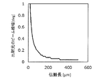
- FIG. 7 is a diagram showing an example of the relationship between the propagation length L p and the beam line width ⁇ of the emitted light.
- the line width of the light beam emitted from one slow light waveguide 10 in which conditions such as the dimensions and the dielectric constant of each component are appropriately set is calculated by changing the propagation length in various ways. The result is shown.
- the beam line width ⁇ of the emitted light becomes narrower.
- the emission angle ⁇ increases. Therefore, as the emission angle ⁇ increases, the beam line width ⁇ of the emitted light decreases.
- the resolution of the scan changes when the emission angle ⁇ changes.
- the present inventors have found the above problems and examined the configuration of an optical device to solve these problems. As a result, it has been found that the above problem can be solved by using a mirror having a special characteristic that has not existed in the past as at least one mirror of the two mirrors in the slow light waveguide.
- the embodiments of the present disclosure described below are based on this finding. Hereinafter, exemplary embodiments of the present disclosure will be described.
- the light 22 propagates through the optical waveguide layer 20 while being reflected by the reflecting surface 30s of the mirror 30 and the reflecting surface 40s of the mirror 40.
- the reflectance of the mirror 30 and the mirror 40 is about 99% even on the light emitting side.
- the mirror 30 and the mirror 40 can be formed from, for example, a DBR.
- An example of the reflection spectrum when light is incident on the reflection surface of the conventional DBR will be described below.
- the incident angle at which light is incident on the reflecting surface corresponds to the propagation angle ⁇ .
- a Synopsys DiffractMod was used to calculate the reflection spectrum.
- the refractive index of the medium on the incident side of the DBR in this example is 1.68.
- the DBR corresponds to the mirror 30 in the slow light waveguide 10, and the medium on the incident side corresponds to the optical waveguide layer 20 in the slow light waveguide 10.
- This DBR has a structure in which 9 high-refractive index layers and 8 low-refractive index layers are alternately laminated.
- Each high refractive index layer has a refractive index of 2.28 and a thickness of 111 nm.
- Each low index of refraction layer has a refractive index of 1.47 and a thickness of 173 nm.
- the reflection spectrum of the conventional DBR shows a reflectance of almost 100% in the stop band as designed, and a low reflectance in the stop band away from the stop band.
- the stop band means a wavelength region in which incident light is strongly reflected by Bragg reflection due to a periodic structure.
- the range in which the incident angle ⁇ is 0 ° or more and 25 ° or less corresponds to the range in which the emission angle ⁇ is 0 ° or more and about 60 ° or less.
- the wavelength dependence of the reflectance of light having a wavelength of ⁇ A is small. Therefore, for the reason described above, the beam line width ⁇ of the emitted light becomes narrower as the emission angle ⁇ increases.
- FIG. 10A the wavelength dependence of the reflectance of light having a wavelength of ⁇ A is small. Therefore, for the reason described above, the beam line width ⁇ of the emitted light becomes narrower as the emission angle ⁇ increases.
- FIG. 10A the wavelength dependence of the reflectance of light having a wavelength of
- the beam line width ⁇ of the emitted light becomes narrower as the emission angle ⁇ increases in the range where the incident angle ⁇ is 0 ° or more and about 15 ° or less, and the incident angle ⁇ is about 15 ° or more and 25 ° or less. In the range, it increases as the emission angle ⁇ increases. In both the examples of FIGS. 10A and 10B, the beam line width ⁇ of the emitted light changes greatly depending on the emission angle ⁇ .
- the present inventors do not significantly change the beam line width ⁇ of the emitted light depending on the emission angle ⁇ by using a mirror whose reflectance gradually decreases as the incident angle ⁇ increases.
- an optical scanning device can be realized. Specifically, by providing an inflection point on the long wavelength side from the maximum value in the reflection spectrum of the mirror, a mirror whose reflectance gradually decreases as the incident angle ⁇ increases has been realized.
- a chirp DBR in which the thicknesses of the high refractive index layer and the low refractive index layer are appropriately adjusted is used as a mirror having an inflection point in the reflection spectrum.
- the term "chirp DBR” means a DBR in which the thickness of the plurality of high refractive index layers and / or the thickness of the plurality of low refractive index layers differs depending on the layer.
- the chap DBR includes not only a DBR in which the thickness of the plurality of high refractive index layers and / or the thickness of the plurality of low refractive index layers gradually increases or decreases along the stacking direction, but also a plurality of high refractive index layers. Also included is a DBR in which the thickness and / or the thickness of the plurality of low index layers varies irregularly or randomly along the stacking direction.
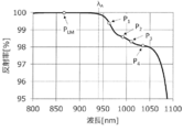
- the reflection spectra in the wavelength range the reflectivity is 95% or more, one maximum point P LM, and inflection points from the inflection point P 1 on the long wavelength side of the maximum point P LM including the P 4.
- the reflectance decreases monotonically on the long wavelength side of the maximum point PLM .
- the inflection point means a point where the second derivative of the reflectance with respect to wavelength becomes zero. At the inflection point, the reflectance changes linearly with respect to the wavelength.
- the local maximum point P LM, and the inflection point P 4 from the inflection point P 1 is present in the wavelength region showing the reflectivity of 95% or more.
- the reflectance may also be present in the wavelength region of 90% or more.
- FIG. 7 shows that the propagation length needs to be about 100 ⁇ m or more in order to reduce the beam line width ⁇ to about 0.2 ° or less.
- FIG. 18 is a diagram showing the relationship between the incident angle ⁇ and the reflectance when the propagation length is 100 ⁇ m. As shown in FIG. 18, in order to maintain the propagation length up to an incident angle of 25 degrees, the reflectance needs to be about 90% or more.
- the reflectance gradually and monotonically decreases in a very high wavelength region where the reflectance is about 95% to 99.9%. More specifically, the reflectance gradually decreases as the incident angle ⁇ increases in the wavelength range.
- the wavelength range is about 940 nm or more and about 1090 nm or less.
- the reflectance does not decrease sharply as shown in FIG. 10B.
- the reflectance is high when the incident angle ⁇ is relatively small, and low when the incident angle ⁇ is relatively large.
- a method for designing a chirp DBR for obtaining a desired reflection spectrum as shown in FIG. 11 is described in, for example, H. A. It is described in Macleod “Thin-Film Optical Filters, 3rd Ed.” (P.193-P.204) IoT Publishing (Bristol and Philadelphia).
- the maximum point PLM and the inflection point of the reflection spectrum may be present in a wavelength region showing a reflectance of 95% or more. With such a configuration, the reflectance can be gradually changed while maintaining a high reflectance.
- the maximum point PLM and the inflection point of the reflection spectrum may be present in a wavelength region showing a reflectance of 90% or more. In the present embodiment, when there is one or more inflection points, the reflectance gradually changes within a range of at least an incident angle ⁇ of 0 ° or more and about 10 ° or less.
- the reflectance when there are two or more inflection points, gradually changes within a range in which the incident angle ⁇ is at least 0 ° or more and about 15 ° or less.
- the change in reflectance with respect to the change in incident angle can be made gentle in a wide angle range.
- a gradual change in the reflectance can be realized while maintaining a high reflectance.
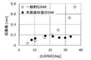
- FIG. 13 is a diagram showing an example of the relationship between the emission angle ⁇ and the propagation length L p .
- the white circles correspond to the case where the mirror 30 in the slow light waveguide 10 is formed from the conventional DBR in the above-mentioned example.
- the black circles correspond to the case where the mirror 30 in the slow light waveguide 10 is formed from the chirp DBR in the above-mentioned example.
- the mirror 40 in the slow light waveguide 10 is formed from a conventional DBR different from the above-mentioned example.
- the DBR has a structure in which 11 high-refractive index layers and 10 low-refractive index layers are alternately laminated.
- the high refractive index layer has a refractive index of 2.28 and a thickness of 107 nm.
- the low refractive index layer has a refractive index of 1.47 and a thickness of 172 nm.
- the refractive index of the optical waveguide layer 20 is 1.68.
- the refractive index of air, which is a medium on the light emitting side, is 1.0.
- the propagation length L p increases as the emission angle ⁇ increases.
- the chirp DBR of the present embodiment it can be seen that the propagation length L p does not change so much even if the emission angle ⁇ increases.
- the chirp DBR of the present embodiment can suppress the dependence of the propagation length L p on the emission angle ⁇ . If the propagation length L p is substantially constant regardless of the emission angle ⁇ , the beam line width ⁇ of the emitted light shown in FIG. 7 is also substantially constant with respect to the emission angle ⁇ . In the example shown in FIG. 13, the propagation length L p is about 150 ⁇ m on average. As shown in FIG.
- the propagation length Lp ⁇ 150 ⁇ m corresponds to the beam line width ⁇ 0.1 ° of the emitted light. Therefore, even if the emission angle ⁇ changes, the beam line width ⁇ of the emitted light can be maintained at about 0.1 degrees. As a result, it is possible to suppress a change in scan resolution due to the emission angle ⁇ . Further, since the beam line width ⁇ of the emitted light is 0.1 °, high resolution can be maintained regardless of the emission angle ⁇ .
- the inflection point P LM1 , the maximum point P LM2 on the longer wavelength side, and the long wavelength side of the maximum point P LM1 in and from the inflection point P 1 on the short wavelength side of the maximum point P LM2 comprises an inflection point P 3.
- the reflectance is increased at the short wavelength side of the maximum point P LM2 a long wavelength side of the maximum point P LM1, after decreases with increasing wavelength. That is, the reflectance does not decrease monotonically on the long wavelength side of the maximum point PLM1 .
- the reflectance decreases monotonically on the long wavelength side of the maximum point PLM2 . Even in this case, the reflectance gradually decreases, more specifically, stepwise as the incident angle ⁇ increases in an extremely high wavelength region where the reflectance is about 99.5% to 99.9%.
- the wavelength range is about 940 nm or more and about 1000 nm or less.
- the dependence of the beam line width ⁇ of the emitted light on the emission angle ⁇ can be suppressed. Further, even if the emission angle ⁇ changes, the beam line width ⁇ of the emitted light can be kept narrow.
- the wavelength ⁇ of the light 22 propagating in the optical waveguide layer 20 is a wavelength equal to or higher than the maximum point and lower than the first inflection point.
- the wavelength range may be included in, for example, a wavelength range of 0.8 ⁇ m or more and 1.2 ⁇ m or less that can be used in the above-mentioned LiDAR system.
- One of the mirror 30 and the mirror 40 may exhibit such a reflection spectrum, or both the mirror 30 and the mirror 40 may exhibit such a reflection spectrum.
- light is emitted from the mirror 30 and the light is reflected by the mirror 40, but the present invention is not limited to this example. Light may be reflected by the mirror 30 and emitted from the mirror 40, or light may be emitted from both the mirror 30 and the mirror 40.
- the wavelength ⁇ of the light 22 propagating in the optical waveguide layer 20 the maximum point P LM, the wavelength represented by the following equation using the first inflection point P 1.
- FIG. 15 is a diagram showing a configuration example of an optical scan device 100 in which elements such as an optical turnout 90, a waveguide array 10A, a phase shifter array 80A, and a light source 130 are integrated on a circuit board (for example, a chip).
- the light source 130 can be, for example, a light emitting element such as a semiconductor laser.
- the light source 130 in this example emits light of a single wavelength having a wavelength of ⁇ in free space.
- the optical turnout 90 branches the light from the light source 130 and introduces it into a waveguide in a plurality of phase shifters.
- an electrode 62A and a plurality of electrodes 62B are provided on the chip.
- a control signal is supplied to the waveguide array 10A from the electrode 62A.
- Control signals are sent from the plurality of electrodes 62B to the plurality of phase shifters 80 in the phase shifter array 80A.
- the electrode 62A and the plurality of electrodes 62B may be connected to a control circuit (not shown) that generates the above control signal.
- the control circuit may be provided on the chip shown in FIG. 15, or may be provided on another chip in the optical scanning device 100.
- all the components shown in FIG. 15 can be integrated on a chip of about 2 mm ⁇ 1 mm.
- FIG. 16 is a schematic view showing a state in which a light beam such as a laser is irradiated far from the optical scanning device 100 to perform a two-dimensional scan.
- the two-dimensional scan is performed by moving the beam spot 310 horizontally and vertically.
- a two-dimensional distance measurement image can be acquired by combining with a known TOF (Time Of Flight) method.
- the TOF method is a method of calculating the flight time of light and obtaining the distance by irradiating a laser and observing the reflected light from an object.
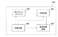
- FIG. 17 is a block diagram showing a configuration example of a LiDAR system 300, which is an example of an optical detection system capable of generating such a ranging image.
- the LiDAR system 300 includes an optical scanning device 100, a photodetector 400, a signal processing circuit 600, and a control circuit 500.
- the photodetector 400 detects the light emitted from the optical scanning device 100 and reflected from the object.
- the photodetector 400 can be, for example, an image sensor sensitive to the wavelength ⁇ of light emitted from the optical scanning device 100, or a photodetector including a light receiving element such as a photodiode.
- the photodetector 400 outputs an electric signal according to the amount of received light.
- the signal processing circuit 600 calculates the distance to the object based on the electric signal output from the photodetector 400, and generates the distance distribution data.
- the distance distribution data is data showing a two-dimensional distribution of distance (that is, a distance measurement image).
- the control circuit 500 is a processor that controls the optical scanning device 100, the photodetector 400, and the signal processing circuit 600.
- the control circuit 500 controls the timing of irradiation of the light beam from the optical scanning device 100 and the timing of exposure and signal readout of the photodetector 400, and instructs the signal processing circuit 600 to generate a distance measurement image.
- the frame rate for acquiring a distance measurement image can be selected from, for example, 60 fps, 50 fps, 30 fps, 25 fps, 24 fps, etc., which are commonly used in moving images. Further, considering the application to an in-vehicle system, the larger the frame rate, the higher the frequency of acquiring the distance measurement image, and the more accurately the obstacle can be detected. For example, when traveling at 60 km / h, an image can be acquired every time the car moves about 28 cm at a frame rate of 60 fps. At a frame rate of 120 fps, an image can be acquired every time the car moves about 14 cm. At a frame rate of 180 fps, an image can be acquired every time the car moves about 9.3 cm.
- the time required to acquire one ranging image depends on the speed of the beam scan. For example, in order to acquire an image having a resolution of 100 ⁇ 100 at 60 fps, it is necessary to perform a beam scan at 1.67 ⁇ s or less for each point.
- the control circuit 500 controls the emission of the light beam by the optical scanning device 100 and the signal storage / reading by the photodetector 400 at an operating speed of 600 kHz.
- the optical scanning device of the present disclosure has almost the same configuration and can also be used as an optical receiving device.
- the optical receiving device includes the same waveguide array 10A as the optical scanning device, and a first adjusting element that adjusts the direction of receivable light.
- Each first mirror 30 of the waveguide array 10A transmits light incident on the opposite side of the first reflecting surface from the third direction.
- Each optical waveguide layer 20 of the waveguide array 10A propagates the light transmitted through the first mirror 30 in the second direction.
- the direction of receivable light can be changed by the first adjusting element changing the refractive index and thickness of the optical waveguide layer 20 in each waveguide element 10 and at least one of the wavelengths of light.
- the second adjusting element for changing the phase difference between the two is provided, the direction of the receivable light can be changed two-dimensionally.
- an optical receiving device in which the light source 130 in the optical scanning device 100 shown in FIG. 15 is replaced with a receiving circuit can be configured.
- the light is sent to the optical turnout 90 through the phase shifter array 80A, finally collected at one place, and sent to the receiving circuit.
- the sensitivity of the optical receiver device can be adjusted by the adjusting elements separately incorporated in the waveguide array and the phase shifter array 80A.
- the directions of the wave vector are opposite.
- the incident light has an optical component in the direction in which the waveguide element 10 extends (X direction in the figure) and an optical component in the arrangement direction of the waveguide elements 10 (Y direction in the figure).
- the sensitivity of the light component in the X direction can be adjusted by an adjusting element incorporated in the waveguide array 10A.
- the sensitivity of the optical component in the arrangement direction of the waveguide element 10 can be adjusted by the adjusting element incorporated in the phase shifter array 80A. From the phase difference ⁇ of the light when the sensitivity of the optical receiving device is maximized, the refractive index n w and the thickness d of the optical waveguide layer 20, ⁇ and ⁇ 0 shown in FIG. 4 can be found. Thereby, the incident direction of the light can be specified.
- the optical device has a first reflecting surface, a first mirror extending along a first direction, and a second reflecting surface facing the first reflecting surface.
- a second mirror extending along the first direction, an optical waveguide located between the first mirror and the second mirror, and propagating light along the first direction.
- the transmittance of the first mirror is higher than the transmittance of the second mirror.
- the reflection spectrum of at least one of the first mirror and the second mirror with respect to the light incident from the normal direction of the reflecting surface is the maximum point in the wavelength region where the reflectance is 90% or more, and the reflection spectrum from the maximum point. Also includes the first and second turning points on the long wavelength side.
- the reflectance of at least one of the first mirror and the second mirror gradually decreases as the incident angle of light increases. Therefore, it is possible to suppress that the beam line width of the light emitted from at least one of the first mirror and the second mirror changes depending on the emission angle.
- the optical device according to the second item has a wavelength of the first inflection point shorter than the wavelength of the second inflection point in the optical device according to the first item.
- the wavelength ⁇ of the light propagating in the optical waveguide layer is a wavelength equal to or higher than the maximum point and equal to or lower than the first inflection point.
- the reflectance of at least one of the first mirror and the second mirror gradually decreases as the incident angle of light increases. As a result, it is possible to suppress the beam line width of the emitted light from changing depending on the emission angle.
- the optical device according to the third item is the optical device according to the first or second item, and the wavelength range is included in 0.8 ⁇ m or more and 1.2 ⁇ m or less.
- This optical device can be applied to LiDAR systems.
- the optical device according to the fourth item is a distributed Bragg reflector in which at least one of the first mirror and the second mirror has a laminated structure in the optical device according to any one of the first to third items. including.
- the optical device according to the fifth item is the optical device according to the fourth item, and the distributed Bragg reflector is a chirp DBR.
- the optical device according to the sixth item is the optical device according to the first item, in which the first mirror has the reflection spectrum.
- the optical scanning device and the optical receiving device in the present disclosure can be used for applications such as a rider system mounted on a vehicle such as an automobile, a UAV, or an AGV.
Landscapes
- Physics & Mathematics (AREA)
- Engineering & Computer Science (AREA)
- General Physics & Mathematics (AREA)
- Computer Networks & Wireless Communication (AREA)
- Radar, Positioning & Navigation (AREA)
- Remote Sensing (AREA)
- Optics & Photonics (AREA)
- Nonlinear Science (AREA)
- Microelectronics & Electronic Packaging (AREA)
- Optical Integrated Circuits (AREA)
- Optical Modulation, Optical Deflection, Nonlinear Optics, Optical Demodulation, Optical Logic Elements (AREA)
Abstract
Description
以下、一例として、2次元スキャンを行う光スキャンデバイスの構成を説明する。ただし、必要以上に詳細な説明は省略する場合がある。例えば、既によく知られた事項の詳細説明および実質的に同一の構成に対する重複する説明を省略することがある。これは、以下の説明が不必要に冗長になることを避け、当業者の理解を容易にするためである。なお、発明者らは、当業者が本開示を十分に理解するために添付図面および以下の説明を提供するのであって、これらによって特許請求の範囲に記載の主題を限定することを意図するものではない。以下の説明において、同一または類似する構成要素については、同じ参照符号を付している。
図2は、1つの導波路素子10の断面の構造および伝搬する光の例を模式的に示す図である。図2では、図1に示すX方向およびY方向に垂直な方向をZ方向とし、導波路素子10のXZ面に平行な断面が模式的に示されている。導波路素子10において、一対のミラー30とミラー40が光導波層20を挟むように配置されている。光導波層20のX方向における一端から導入された光22は、光導波層20の上面(図2における上側の表面)に設けられた第1のミラー30の第1の反射面30sおよび下面(図2における下側の表面)に設けられた第2のミラー40の第2の反射面40sによって反射を繰り返しながら光導波層20内を伝搬する。第1のミラー30の光透過率は、第2のミラー40の光透過率よりも高い。このため、主に第1のミラー30の出射面30esから光の一部を出力することができる。以下では、第1の反射面30sを、単に「反射面30s」と称し、第2の反射面40sを、単に「反射面40s」と称することがある。
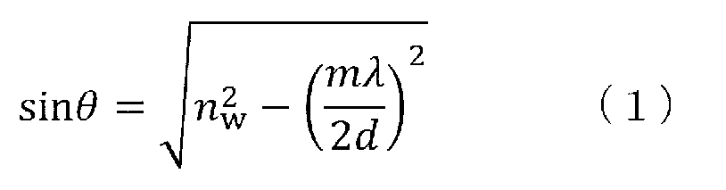
複数の導波路素子10が一方向に配列された導波路アレイにおいて、それぞれの導波路素子10から出射される光の干渉により、光の出射方向は変化する。各導波路素子10に供給する光の位相を調整することにより、光の出射方向を変化させることができる。以下、その原理を説明する。
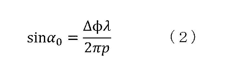
それぞれの導波路素子10から出射される光の位相を制御するために、例えば、導波路素子10に光を導入する前段に、光の位相を変化させる位相シフタが設けられ得る。本開示の光スキャンデバイス100は、複数の導波路素子10のそれぞれに接続された複数の位相シフタと、各位相シフタを伝搬する光の位相を調整する第2調整素子とを備える。各位相シフタは、複数の導波路素子10の対応する1つにおける光導波層20に直接的にまたは他の導波路を介して繋がる導波路を含む。第2調整素子は、複数の位相シフタから複数の導波路素子10へ伝搬する光の位相の差をそれぞれ変化させることにより、複数の導波路素子10から出射される光の方向(すなわち、第3の方向D3)を変化させる。以下の説明では、導波路アレイと同様に、配列された複数の位相シフタを「位相シフタアレイ」と称することがある。
スローライト導波路10から出射される光のビーム線幅は、スキャンの分解能を決定する。ビーム線幅が狭くなると、スキャンの分解能は向上し、ビーム線幅が広くなると、スキャンの分解能は低下する。以下、従来のスローライト導波路10から出射される光のビーム線幅と、出射角度との関係を説明する。

図15は、回路基板(たとえば、チップ)上に光分岐器90、導波路アレイ10A、位相シフタアレイ80A、および光源130などの素子を集積した光スキャンデバイス100の構成例を示す図である。光源130は、例えば、半導体レーザーなどの発光素子であり得る。この例における光源130は、自由空間における波長がλである単一波長の光を出射する。光分岐器90は、光源130からの光を分岐して複数の位相シフタにおける導波路に導入する。図15に示す例において、チップ上には電極62Aと、複数の電極62Bとが設けられている。導波路アレイ10Aには、電極62Aから制御信号が供給される。位相シフタアレイ80Aにおける複数の位相シフタ80には、複数の電極62Bから制御信号がそれぞれ送られる。電極62A、および複数の電極62Bは、上記の制御信号を生成する不図示の制御回路に接続され得る。制御回路は、図15に示すチップ上に設けられていてもよいし、光スキャンデバイス100における他のチップに設けられていてもよい。
本開示の光スキャンデバイスは、ほぼ同一の構成で、光受信デバイスとしても用いることができる。光受信デバイスは、光スキャンデバイスと同一の導波路アレイ10Aと、受信可能な光の方向を調整する第1調整素子とを備える。導波路アレイ10Aの各第1のミラー30は、第3の方向から第1の反射面の反対側に入射する光を透過させる。導波路アレイ10Aの各光導波層20は、第2の方向に第1のミラー30を透過した光を伝搬させる。第1調整素子が各導波路素子10における前記光導波層20の屈折率および厚さ、ならびに光の波長の少なくとも1つを変化させることにより、受信可能な光の方向を変化させることができる。さらに、光受信デバイスが、光スキャンデバイスと同一の複数の位相シフタ80、または80aおよび80bと、複数の導波路素子10から複数の位相シフタ80、または80aおよび80bを通過して出力される光の位相の差をそれぞれ変化させる第2調整素子を備える場合には、受信可能な光の方向を2次元的に変化させることができる。
11 光導波路
10A 導波路アレイ
15、15a、15b、15c、15m グレーティング
20 光導波層
22 誘電体部材
30 第1のミラー
40 第2のミラー
30es 出射面
30s 第1の反射面
40s 第2の反射面
51 誘電体層
62a、62b、62A、62B 電極
73 複数の隔壁
80 位相シフタ
80A 位相シフタアレイ
90 光分岐器
100 光スキャンデバイス
111 接続領域
112 非接続領域
110 導波路アレイの駆動回路
130 光源
210 位相シフタアレイの駆動回路
310 ビームスポット
400 光検出器
500 制御回路
600 信号処理回路
Claims (8)
- 第1の反射面を有し、第1の方向に沿って延びる第1のミラーと、
前記第1の反射面に対向する第2の反射面を有し、前記第1の方向に沿って延びる第2のミラーと、
前記第1のミラーと前記第2のミラーの間に位置し、光を前記第1の方向に沿って伝搬させる光導波層と、
を備え、
前記第1のミラーの透過率は、前記第2のミラーの透過率よりも高く、
前記第1のミラーおよび前記第2のミラーの少なくとも一方の、反射面の法線方向から入射する光に対する反射スペクトルは、反射率が90%以上である波長域において極大点、および前記極大点よりも長波長側に第1の変曲点および第2の変曲点を含む、
光デバイス。 - 前記第1の変曲点の波長は前記第2の変曲点の波長よりも短く、
前記光導波層を伝搬する前記光の波長λは、前記極大点以上、前記第1の変曲点以下の波長である、
請求項1に記載の光デバイス。 - 前記波長域は、0.8μm以上1.2μm以下に含まれる、
請求項1または2に記載の光デバイス。 - 前記第1のミラーおよび前記第2のミラーの少なくとも一方は、積層構造を備える分布ブラッグ反射器を含む、
請求項1から3のいずれかに記載の光デバイス。 - 前記分布ブラッグ反射器は、チャープDBRである
請求項4に記載の光デバイス。 - 前記第1のミラーが前記反射スペクトルを有する、
請求項1に記載の光デバイス。 - 第1の反射面を有し、第1の方向に沿って延びる第1のミラーと、
前記第1の反射面に対向する第2の反射面を有し、前記第1の方向に沿って延びる第2のミラーと、
前記第1のミラーと前記第2のミラーの間に位置し、光を前記第1の方向に沿って伝搬させる光導波層と、
を備え、
前記第1のミラーの透過率は、前記第2のミラーの透過率よりも高く、
前記第1のミラーおよび前記第2のミラーの少なくとも一方の、反射面の法線方向から入射する光に対する反射スペクトルは、反射率が90%以上である波長域において極大点PLM、および前記極大点よりも長波長側に第1の変曲点P1および第2の変曲点P2を含み、
前記第1のミラーを介して出射した光が空間をスキャンするように偏向される、
光スキャンデバイス。 - 前記スキャンに用いられる波長λが、
(PLM+P1)/2 < λ < P1
を満たす、請求項7に記載の光スキャンデバイス。
Priority Applications (4)
| Application Number | Priority Date | Filing Date | Title |
|---|---|---|---|
| JP2021518328A JP7486105B2 (ja) | 2019-05-09 | 2020-04-14 | 光デバイスおよび光検出システム |
| EP20802445.5A EP3968084B1 (en) | 2019-05-09 | 2020-04-14 | Optical device and optical detection system |
| CN202080023953.3A CN113614632B (zh) | 2019-05-09 | 2020-04-14 | 光设备及光检测系统 |
| US17/488,391 US12038606B2 (en) | 2019-05-09 | 2021-09-29 | Optical device and photodetection system |
Applications Claiming Priority (2)
| Application Number | Priority Date | Filing Date | Title |
|---|---|---|---|
| JP2019-089232 | 2019-05-09 | ||
| JP2019089232 | 2019-05-09 |
Related Child Applications (1)
| Application Number | Title | Priority Date | Filing Date |
|---|---|---|---|
| US17/488,391 Continuation US12038606B2 (en) | 2019-05-09 | 2021-09-29 | Optical device and photodetection system |
Publications (1)
| Publication Number | Publication Date |
|---|---|
| WO2020226031A1 true WO2020226031A1 (ja) | 2020-11-12 |
Family
ID=73051127
Family Applications (1)
| Application Number | Title | Priority Date | Filing Date |
|---|---|---|---|
| PCT/JP2020/016394 Ceased WO2020226031A1 (ja) | 2019-05-09 | 2020-04-14 | 光デバイスおよび光検出システム |
Country Status (5)
| Country | Link |
|---|---|
| US (1) | US12038606B2 (ja) |
| EP (1) | EP3968084B1 (ja) |
| JP (1) | JP7486105B2 (ja) |
| CN (1) | CN113614632B (ja) |
| WO (1) | WO2020226031A1 (ja) |
Families Citing this family (1)
| Publication number | Priority date | Publication date | Assignee | Title |
|---|---|---|---|---|
| US12164097B2 (en) * | 2020-02-24 | 2024-12-10 | Massachusetts Institute Of Technology | Bragg light source for dark-field imaging devices |
Citations (6)
| Publication number | Priority date | Publication date | Assignee | Title |
|---|---|---|---|---|
| JPH10233528A (ja) * | 1996-12-18 | 1998-09-02 | Sharp Corp | 半導体発光ダイオード |
| JPH1187767A (ja) * | 1997-09-11 | 1999-03-30 | Sharp Corp | 発光ダイオード |
| JP2006047872A (ja) * | 2004-08-06 | 2006-02-16 | Fuji Xerox Co Ltd | 光スイッチ並びにそれを用いた光分配装置及び光多重化装置 |
| US20120230352A1 (en) * | 2011-03-10 | 2012-09-13 | Coherent, Inc. | High-power cw fiber-laser |
| JP2013016591A (ja) | 2011-07-01 | 2013-01-24 | Denso Corp | 光偏向素子および光偏向モジュール |
| US20180224709A1 (en) | 2017-02-09 | 2018-08-09 | Panasonic Intellectual Property Management Co., Ltd. | Optical scanning device including waveguide array |
Family Cites Families (14)
| Publication number | Priority date | Publication date | Assignee | Title |
|---|---|---|---|---|
| US5305336A (en) * | 1992-01-29 | 1994-04-19 | At&T Bell Laboratories | Compact optical pulse source |
| JP2005227324A (ja) * | 2004-02-10 | 2005-08-25 | Matsushita Electric Ind Co Ltd | 表示素子および表示装置 |
| KR20070097404A (ko) | 2005-01-20 | 2007-10-04 | 로무 가부시키가이샤 | 광 변조막을 갖는 광 제어 장치 |
| JP2006220746A (ja) * | 2005-02-08 | 2006-08-24 | Rohm Co Ltd | 光制御装置およびそれに用いる構造体 |
| WO2013168266A1 (ja) | 2012-05-10 | 2013-11-14 | パイオニア株式会社 | 駆動装置 |
| EP3388892A1 (en) | 2013-01-08 | 2018-10-17 | Massachusetts Institute Of Technology | Optical phased arrays |
| JP5910970B2 (ja) | 2013-01-29 | 2016-04-27 | 日本電信電話株式会社 | 波長選択スイッチ |
| CN108700790B (zh) * | 2016-01-22 | 2021-10-22 | 国立大学法人横浜国立大学 | 光偏转器及激光雷达装置 |
| EP3521920B1 (en) * | 2016-09-29 | 2021-09-29 | Panasonic Intellectual Property Management Co., Ltd. | Optical scan device, light receiving device, and optical detection system |
| JP2018124271A (ja) * | 2017-01-31 | 2018-08-09 | パナソニックIpマネジメント株式会社 | 撮像システム |
| JP7018564B2 (ja) * | 2017-02-09 | 2022-02-14 | パナソニックIpマネジメント株式会社 | 光スキャンデバイス、光受信デバイス、および光検出システム |
| KR102162047B1 (ko) * | 2017-02-17 | 2020-10-06 | 호쿠요덴키 가부시키가이샤 | 물체 포착 장치 |
| CN108627974A (zh) | 2017-03-15 | 2018-10-09 | 松下知识产权经营株式会社 | 光扫描系统 |
| JP2018156059A (ja) | 2017-03-15 | 2018-10-04 | パナソニックIpマネジメント株式会社 | 光スキャンシステム |
-
2020
- 2020-04-14 CN CN202080023953.3A patent/CN113614632B/zh active Active
- 2020-04-14 EP EP20802445.5A patent/EP3968084B1/en active Active
- 2020-04-14 JP JP2021518328A patent/JP7486105B2/ja active Active
- 2020-04-14 WO PCT/JP2020/016394 patent/WO2020226031A1/ja not_active Ceased
-
2021
- 2021-09-29 US US17/488,391 patent/US12038606B2/en active Active
Patent Citations (6)
| Publication number | Priority date | Publication date | Assignee | Title |
|---|---|---|---|---|
| JPH10233528A (ja) * | 1996-12-18 | 1998-09-02 | Sharp Corp | 半導体発光ダイオード |
| JPH1187767A (ja) * | 1997-09-11 | 1999-03-30 | Sharp Corp | 発光ダイオード |
| JP2006047872A (ja) * | 2004-08-06 | 2006-02-16 | Fuji Xerox Co Ltd | 光スイッチ並びにそれを用いた光分配装置及び光多重化装置 |
| US20120230352A1 (en) * | 2011-03-10 | 2012-09-13 | Coherent, Inc. | High-power cw fiber-laser |
| JP2013016591A (ja) | 2011-07-01 | 2013-01-24 | Denso Corp | 光偏向素子および光偏向モジュール |
| US20180224709A1 (en) | 2017-02-09 | 2018-08-09 | Panasonic Intellectual Property Management Co., Ltd. | Optical scanning device including waveguide array |
Non-Patent Citations (2)
| Title |
|---|
| H. A. MACLEOD: "Thin-film Optical Filters", LOP PUBLISHING, pages: 193 - 204 |
| See also references of EP3968084A4 |
Also Published As
| Publication number | Publication date |
|---|---|
| US12038606B2 (en) | 2024-07-16 |
| CN113614632B (zh) | 2025-08-01 |
| EP3968084A1 (en) | 2022-03-16 |
| CN113614632A (zh) | 2021-11-05 |
| JP7486105B2 (ja) | 2024-05-17 |
| EP3968084A4 (en) | 2022-06-29 |
| JPWO2020226031A1 (ja) | 2020-11-12 |
| EP3968084B1 (en) | 2024-10-16 |
| US20220019022A1 (en) | 2022-01-20 |
Similar Documents
| Publication | Publication Date | Title |
|---|---|---|
| JP7796361B2 (ja) | 光デバイス | |
| JP7429928B2 (ja) | 光デバイスおよび光検出システム | |
| WO2020084850A1 (ja) | 光検出システム | |
| US12147094B2 (en) | Optical device and photodetection system | |
| CN113614571B (zh) | 光设备、光检测系统及其制造方法 | |
| JP7486105B2 (ja) | 光デバイスおよび光検出システム | |
| WO2022113427A1 (ja) | 光デバイスおよび光検出システム | |
| JP6931237B2 (ja) | 光偏向デバイス、及びライダー装置 | |
| JP7394395B2 (ja) | 光デバイスおよび光検出システム | |
| US20250389949A1 (en) | Optical device | |
| JP7519584B2 (ja) | 光デバイス | |
| WO2023218703A1 (ja) | 光デバイスおよび光検出システム |
Legal Events
| Date | Code | Title | Description |
|---|---|---|---|
| 121 | Ep: the epo has been informed by wipo that ep was designated in this application |
Ref document number: 20802445 Country of ref document: EP Kind code of ref document: A1 |
|
| ENP | Entry into the national phase |
Ref document number: 2021518328 Country of ref document: JP Kind code of ref document: A |
|
| NENP | Non-entry into the national phase |
Ref country code: DE |
|
| ENP | Entry into the national phase |
Ref document number: 2020802445 Country of ref document: EP Effective date: 20211209 |
|
| WWG | Wipo information: grant in national office |
Ref document number: 202080023953.3 Country of ref document: CN |