WO2020235535A1 - 電子部品取付装置、電子装置の製造方法及びストラップの製造方法 - Google Patents
電子部品取付装置、電子装置の製造方法及びストラップの製造方法 Download PDFInfo
- Publication number
- WO2020235535A1 WO2020235535A1 PCT/JP2020/019679 JP2020019679W WO2020235535A1 WO 2020235535 A1 WO2020235535 A1 WO 2020235535A1 JP 2020019679 W JP2020019679 W JP 2020019679W WO 2020235535 A1 WO2020235535 A1 WO 2020235535A1
- Authority
- WO
- WIPO (PCT)
- Prior art keywords
- electronic components
- electronic component
- electronic
- adherend
- transfer mechanism
- Prior art date
- Legal status (The legal status is an assumption and is not a legal conclusion. Google has not performed a legal analysis and makes no representation as to the accuracy of the status listed.)
- Ceased
Links
Images










Classifications
-
- H—ELECTRICITY
- H05—ELECTRIC TECHNIQUES NOT OTHERWISE PROVIDED FOR
- H05K—PRINTED CIRCUITS; CASINGS OR CONSTRUCTIONAL DETAILS OF ELECTRIC APPARATUS; MANUFACTURE OF ASSEMBLAGES OF ELECTRICAL COMPONENTS
- H05K13/00—Apparatus or processes specially adapted for manufacturing or adjusting assemblages of electric components
- H05K13/04—Mounting of components, e.g. of leadless components
- H05K13/0478—Simultaneously mounting of different components
- H05K13/0482—Simultaneously mounting of different components using templates; using magazines, the configuration of which corresponds to the sites on the boards where the components have to be attached
-
- H—ELECTRICITY
- H05—ELECTRIC TECHNIQUES NOT OTHERWISE PROVIDED FOR
- H05K—PRINTED CIRCUITS; CASINGS OR CONSTRUCTIONAL DETAILS OF ELECTRIC APPARATUS; MANUFACTURE OF ASSEMBLAGES OF ELECTRICAL COMPONENTS
- H05K13/00—Apparatus or processes specially adapted for manufacturing or adjusting assemblages of electric components
- H05K13/0053—Arrangements for assisting the manual mounting of components, e.g. special tables or light spots indicating the place for mounting
-
- H—ELECTRICITY
- H05—ELECTRIC TECHNIQUES NOT OTHERWISE PROVIDED FOR
- H05K—PRINTED CIRCUITS; CASINGS OR CONSTRUCTIONAL DETAILS OF ELECTRIC APPARATUS; MANUFACTURE OF ASSEMBLAGES OF ELECTRICAL COMPONENTS
- H05K13/00—Apparatus or processes specially adapted for manufacturing or adjusting assemblages of electric components
- H05K13/04—Mounting of components, e.g. of leadless components
- H05K13/0404—Pick-and-place heads or apparatus, e.g. with jaws
- H05K13/0408—Incorporating a pick-up tool
- H05K13/0409—Sucking devices
-
- H—ELECTRICITY
- H05—ELECTRIC TECHNIQUES NOT OTHERWISE PROVIDED FOR
- H05K—PRINTED CIRCUITS; CASINGS OR CONSTRUCTIONAL DETAILS OF ELECTRIC APPARATUS; MANUFACTURE OF ASSEMBLAGES OF ELECTRICAL COMPONENTS
- H05K13/00—Apparatus or processes specially adapted for manufacturing or adjusting assemblages of electric components
- H05K13/04—Mounting of components, e.g. of leadless components
- H05K13/0404—Pick-and-place heads or apparatus, e.g. with jaws
- H05K13/0408—Incorporating a pick-up tool
- H05K13/041—Incorporating a pick-up tool having multiple pick-up tools
-
- H—ELECTRICITY
- H05—ELECTRIC TECHNIQUES NOT OTHERWISE PROVIDED FOR
- H05K—PRINTED CIRCUITS; CASINGS OR CONSTRUCTIONAL DETAILS OF ELECTRIC APPARATUS; MANUFACTURE OF ASSEMBLAGES OF ELECTRICAL COMPONENTS
- H05K13/00—Apparatus or processes specially adapted for manufacturing or adjusting assemblages of electric components
- H05K13/04—Mounting of components, e.g. of leadless components
- H05K13/043—Feeding one by one by other means than belts
-
- H—ELECTRICITY
- H05—ELECTRIC TECHNIQUES NOT OTHERWISE PROVIDED FOR
- H05K—PRINTED CIRCUITS; CASINGS OR CONSTRUCTIONAL DETAILS OF ELECTRIC APPARATUS; MANUFACTURE OF ASSEMBLAGES OF ELECTRICAL COMPONENTS
- H05K13/00—Apparatus or processes specially adapted for manufacturing or adjusting assemblages of electric components
- H05K13/04—Mounting of components, e.g. of leadless components
- H05K13/0478—Simultaneously mounting of different components
Definitions
- the present invention relates to an electronic component mounting device, a method for manufacturing an electronic device, and a method for manufacturing a strap.
- a method for manufacturing an electronic device which includes a step of attaching one or more of a large number of electronic components closely placed at a predetermined location to an adherend to manufacture the electronic device.
- a manufacturing method may be used when attaching an IC chip to an electronic device.
- a semiconductor wafer is cut using a laser or the like to break up a large number of chips into individual pieces.
- a large number of IC chips are arranged in a plurality of columns and a plurality of rows without gaps.
- a plurality of IC chips are placed on a stretchable sheet, and the intervals between the IC chips are adjusted by stretching the sheets, and a plurality of antennas and the like are arranged at predetermined intervals.
- a method of attaching to each antenna of the formed antenna sheet (adhesion) has been proposed.
- a method of using a plate having a plurality of recesses into which the electronic component is fitted is also known.
- recesses of the plate are formed at positions corresponding to a plurality of attachment positions on the adherend, a large number of electronic components are placed on the plate, and the plate is vibrated or tilted to vibrate or tilt the plate.
- An electronic component is fitted into the recess of the recess, and the electronic component of the recess is attached to the adherend.
- the antenna can be used.
- the IC chip cannot be attached properly.
- the distance between adjacent IC chips will change, so it will be necessary to consider the type of sheet and elasticity each time such a change is made, resulting in a wide variety of products. If it is dealt with, the cost may increase.
- the present invention has been made in view of such inconveniences, and the subject of the present invention is that electronic components can be attached to an adherend accurately and efficiently, and the type of adherend can be easily changed. It is an object of the present invention to provide an electronic component mounting device and a method for manufacturing the electronic device.
- the invention made to solve the above problems is An electronic component mounting device that mounts a plurality of electronic components placed at predetermined locations on an adherend at different intervals.
- a take-out mechanism for taking out some of the plurality of electronic components from the plurality of electronic components placed at the predetermined locations, and The electronic components taken out by the take-out mechanism are conveyed, and the electronic components are moved so as to have different intervals for attaching the plurality of electronic components to the adherend before reaching the adherend, and the electronic components are moved.
- a transport mechanism that transports to the adherend and A mounting transfer mechanism that attaches the electronic components transported by the transfer mechanism to the predetermined position of the adherend, and To be equipped.
- the take-out mechanism takes out the plurality of the electronic components, and the transport mechanism transports the taken-out electronic components and before reaching the adherend, the plurality of electronic components.
- the electronic components are moved so as to be attached to the adherend at different intervals, the electronic components are transported to the adherend, and the mounting transfer mechanism transfers the electronic components transported by the transport mechanism to the predetermined adherend. Install in position.
- the electronic component mounting device can mount the plurality of electronic components on the adherend at the same time, so that the electronic components can be mounted efficiently.
- the transport mechanism simply changes the interval between the electronic components. Can be accommodated.
- the electronic components can be attached with higher accuracy than the conventional one using a stretchable sheet.
- the electronic components are arranged in a plurality of rows having different intervals, and the electronic components taken out by the take-out mechanism are held, and these electronic components are held. It is preferable to have a first transfer mechanism for moving the components to the alignment section and a second transfer mechanism for transferring the electronic components moved to the alignment section to the mounting transfer mechanism.
- the electronic components can be temporarily placed in a plurality of rows having the above-mentioned different intervals in the alignment portion between the take-out mechanism and the mounting transfer mechanism. Therefore, for example, inspection of electronic components Even if the above is performed, the influence on the mounting operation can be reduced. Further, since the first transfer mechanism can temporarily place the electronic component in the alignment portion in an arrangement that is easy to attach to the adherend, the attachment efficiency can be improved.
- the first transfer mechanism is placed in the alignment portion by moving a plurality of rows of the electronic components side by side in a state where the electronic components have different intervals between the rows, and placing the second transfer mechanism. Transports a plurality of electronic components in the same row from the alignment unit while maintaining a state in which the electronic components are spaced apart from each other, and the mounting transfer mechanism transports the electronic components between the electronic components. It is preferable to mount them on the adherend at different intervals.
- the first transfer mechanism simultaneously sucks and takes out a plurality of electronic components from the mounting table, moves the electronic components to the alignment unit, and mounts the electronic components.
- the placement on the alignment portion by the first transfer mechanism is repeated a plurality of times, and the electronic components are arranged in a plurality of rows with the above-mentioned different spacing between the rows.
- the second transfer mechanism simultaneously sucks and takes out a plurality of electronic components in the same row having the above-mentioned different intervals between the columns from the alignment unit, and simultaneously mounts the plurality of electronic components in the same row on the adherend. Place.
- the electronic component mounting device can mount a plurality of electronic components on the adherend at the same time, so that the electronic components can be mounted efficiently.
- the electronic component mounting device even if the distance between the attachment positions of the adherend is changed due to a change in the type of the adherend, etc., between the rows of electronic components to be placed on the alignment portion. It can be dealt with simply by changing the interval. Further, the electronic components can be attached with higher accuracy than the conventional one using a stretchable sheet.
- the second transfer mechanism may hold and transfer the electronic components arranged in the same row at predetermined row intervals such as odd-numbered rows and even-numbered rows.
- the second transfer mechanism includes a take-out means for simultaneously sucking a plurality of electronic components in the same row from the alignment portion, and a temporary placement portion for delivering a plurality of electronic parts in the same row taken out by the take-out means. It is preferable that the attachment / transfer mechanism attracts a plurality of the electronic components in the same row delivered to the temporary placement portion and attaches them to the adherend. Since the second transfer mechanism has the temporary storage portion in this way, the timing of receiving the electronic component from the alignment unit by the extraction means, the timing of delivery to the temporary installation portion by the extraction means, and the timing of delivery from the temporary installation portion by the mounting transfer means. It is possible to adjust the timing of receiving the electronic component and the timing of placing the electronic component on the adherend by the mounting transfer means, whereby the efficiency of the mounting work of the electronic component can be further improved.
- the second transfer mechanism mounts a plurality of the electronic components in the same row from the take-out means, and inverts the placed electronic components and delivers them to the temporary storage portion. It is preferable to further have an inversion means.
- the front and back may be distinguished (for example, a circuit may be formed on only one surface), and even in such a case, the second transfer mechanism means uses the reversing means. By having it, a desired surface of the electronic component can be placed on the adherend.
- the temporary placement portion is provided with a correction means for correcting the position of the placed electronic component.
- the electronic component can be placed on the adherend at a more accurate position than the state in which the temporary placement portion is placed on the alignment portion.
- the second transfer mechanism simultaneously adsorbs a plurality of rows of electronic components from the alignment portion. As a result, the efficiency of the work of taking out the electronic components from the alignment portion by the second transfer mechanism can be improved.
- the second transfer mechanism places a plurality of rows of the electronic components on the adherend at the same time. As a result, the efficiency of mounting work of electronic components by the second transfer mechanism can be improved.
- the alignment unit moves the placed electronic component between the first transfer mechanism and the first delivery position for delivering the electronic component and the second transfer mechanism and the second delivery position for delivering the electronic component. It is preferable to move. As a result, the degree of freedom of the arrangement location between the component of the first transfer mechanism and the component of the second transfer mechanism is improved.
- the first transfer mechanism is provided with a suction holding device capable of changing the number of electronic components to be sucked. This makes it possible to change the number of electronic components attracted by the first transfer mechanism from the mounting table.
- the direction in which the plurality of electronic components held by the second transfer mechanism are lined up is preferably parallel to the direction in which the plurality of adherends to be attached are lined up.
- the transport mechanism has a plurality of the alignment portions and can be positioned at the mounting position and the taking-out position, respectively. Since the transport mechanism can be positioned in the mounting position and the taking-out position, it is possible to always position one of the rearranging tables in both positions. Therefore, electronic components can always be placed and taken out, which is efficient. Moreover, since the loading and unloading can be efficiently separated, if one loading position and two loadings are used, the loading operation can always be performed, which is efficient.
- the second transfer mechanism may transfer in a state where the intervals between the electronic components are different from each other. As a result, the electronic component can be easily and surely transferred by the second transfer mechanism.
- the second transfer mechanism transports a plurality of rows of electronic components in one transport operation, and the patterns of spacing between the plurality of rows of electronic components are different. As a result, it is possible to transfer a plurality of rows of electronic components having different interval patterns by one transfer operation.
- the take-out mechanism takes out the plurality of electronic components in a line.
- the electronic component may be an IC chip used in an RFID device or a strap on which an IC chip is mounted. Thereby, the RFID device can be easily and surely manufactured by the electronic component mounting device.
- the plurality of electronic components may be placed in close contact with the above-mentioned stand. As a result, a large number of electronic components can be mounted on the mounting table.
- "closeness” means that they are closely attached so that there is no gap.
- the take-out mechanism may adsorb and hold the electronic component. As a result, a plurality of electronic components can be easily and surely taken out by the taking-out mechanism.
- the attachment / transfer mechanism may attach a plurality of the electronic components to the adherend at the same height position. As a result, a plurality of electronic components can be easily and surely attached to the adherend by the attachment / transfer mechanism.
- the electronic component mounting device may further include an adherend position confirming member for confirming the adhered position of the adherend before the electronic component is attached.
- the electronic component mounting device calculates the distance between the adherend positions based on the adhered position of the adherend confirmed by the adherend position confirmation member, and attaches the electronic component based on the calculated interval. Can be done.
- the electronic component attachment device can also be suitably used for an adherend having a repeating pattern in which the adherence positions are different in the row direction.
- the electronic component mounting device can be suitably used even for an adherend in which the patterns of different intervals are not repeated.
- the invention made to solve the above problems is A method of manufacturing an electronic device in which a plurality of electronic components placed in a predetermined place are attached to an adherend at different intervals.
- some of the plurality of electronic components are taken out from the plurality of electronic components placed at predetermined locations, and the taken-out electronic components are transported before reaching the adherend. Easy and reliable by moving each electronic component so that the distance between adjacent electronic components is different from each other, transporting the electronic component to the adherend, and attaching the transported electronic component to a predetermined position of the adherend. Electronic devices can be manufactured.
- the transfer step includes a step of attaching the electronic component with a first interval pattern and a step of attaching the electronic component with a second interval pattern different from the first interval pattern. It is good to have.
- a plurality of electronic components are efficiently attached to a predetermined position of the adherend. By attaching it, it is possible to manufacture an electronic device more easily and reliably.
- the invention made to solve the above problems is A method of manufacturing an electronic device that simultaneously attaches multiple electronic components to an adherend at different intervals.
- a take-out process that takes out and holds multiple electronic components from a predetermined location, The first transport step of transporting the plurality of the electronic components taken out in the take-out step to the alignment portion and placing the electronic components on the alignment portion, A second transport step of transporting the electronic component placed on the alignment portion to the adherend while holding the electronic component, and The mounting transfer step of attaching the electronic component transported in the second transfer step to a predetermined position of the adherend, and To be equipped.
- a plurality of electronic components are taken out and held from a predetermined location, the plurality of the taken-out electronic components are conveyed to an aligning portion, and the electronic components are placed on the aligning portion.
- An electronic device can be easily and surely manufactured by transporting the electronic component placed on the alignment portion to the adherend while holding the electronic component, and attaching the transported electronic component to a predetermined position of the adherend. Can be done.
- the electronic components are placed on the aligning portion so that a plurality of the electronic components can be arranged and transported in a row in the second transfer step. Good. As a result, a plurality of electronic components can be easily and reliably transported in the second transport step.
- the invention made to solve the above problems is A method of manufacturing an electronic device that simultaneously attaches multiple electronic components to an adherend at different intervals.
- the take-out process of taking out multiple electronic components from a predetermined location A holding step of holding the plurality of electronic components taken out in the taking-out step side by side in a transport mechanism at different intervals when the plurality of electronic components are attached to the adherend.
- a transport process in which the electronic component is held by the transport mechanism and transported to the adherend The mounting transfer step of attaching the electronic component transported in the transfer process to a predetermined position of the adherend, and To be equipped.
- a plurality of electronic components are taken out from a predetermined location, and the plurality of the taken-out electronic components are held side by side in a transport mechanism at predetermined intervals, and the transport mechanism is used to hold the electronic components.
- An electronic device can be easily and surely manufactured by transporting the transported electronic component to the adherend in a held state and attaching the transported electronic component to a predetermined position of the adherend.
- the invention made to solve the above problems is A method of manufacturing straps used in RFID devices.
- a process of transporting an electrode sheet on which a pair of electrodes are formed with a predetermined gap along the longitudinal direction to a predetermined position and The process of arranging multiple IC chips in multiple rows at intervals, A step of transporting the plurality of IC chips to the predetermined position while holding them in a row state, contacting the pair of electrodes, and placing the plurality of IC chips in the gaps of the pair of electrodes.
- the IC chips In the method of manufacturing the strap, by mounting a plurality of IC chips on the electrode sheet transported to a predetermined position by the transport process, the IC chips come into contact with the pair of electrodes and a pair of electrodes.
- An electronic device arranged in a gap between electrodes can be easily and reliably manufactured.
- the electronic component mounting device, the method for manufacturing the electronic device, and the method for manufacturing the strap of the present invention can accurately and efficiently attach the electronic component to the adherend, and when the type of the adherend is changed. Can be easily dealt with.
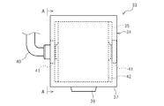
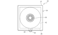
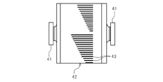
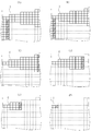
- FIG. 3 is a cross-sectional view taken along the line AA of FIG. It is a bottom view of the collet part used for a suction holding device. It is a side view of the displacement body used for a suction holding device. It is a schematic enlarged plan view of the main part for sequentially schematically explaining the state of the mounting table in the state where the electronic component is taken out in the electronic component mounting device.
- FIG. 1 It is a schematic enlarged plan view of the main part for sequentially schematically explaining the state of the mounting table in the state where the electronic component is taken out in the electronic component mounting device. It is a schematic plan view for demonstrating the internal structure of the housing of the suction holding device of another embodiment of this invention. It is a schematic side view of the suction holding device of another embodiment of this invention. It is a schematic front view of the rotating body used for the suction holding device of another embodiment. It is a schematic perspective view of the rotating body of another embodiment of this invention. It is a schematic front view of the suction holding device of another embodiment of this invention.
- FIG. 5 is an enlarged plan view of a schematic main part for schematically explaining a state of a mounting table according to another embodiment of the present invention.
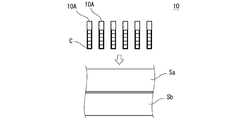
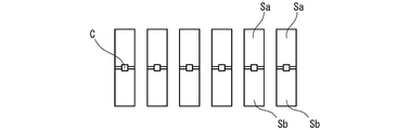
- FIG. 5 is an enlarged plan view of a schematic main part for schematically explaining a state of a mounting table according to another embodiment of the present invention. It is a schematic explanatory drawing for demonstrating the state before placing an IC chip on an electrode sheet in the method of manufacturing a strap of another embodiment of this invention.
- the electronic component mounting device 100 is an electronic component mounting device that mounts a plurality of electronic components placed at predetermined locations on an adherend at different intervals.
- the electronic component mounting device 100 takes out an electronic component in a state where a large number of electronic components C are closely arranged in a state of being arranged in a plurality of columns and a plurality of rows, and covers the electronic component (here, an IC chip C). It is a device attached to a kimono (RFID tag A in this embodiment).
- “row” and “column” mean an array in the X direction and an array in the Y direction in FIG. 1, respectively.
- the IC chip C is formed by cutting, for example, a thin disk disk-shaped semiconductor wafer W on which a large number of circuit patterns are formed in a grid pattern.
- the electronic component mounting device 100 is a device that takes out a plurality of IC chips C in a row from a large number of IC chips C arranged in a plurality of columns and a plurality of rows without gaps, and attaches each of the IC chips C to the RFID tag A. is there. It should be noted that each figure is a schematic drawing and schematically shows the size, number and the like of each member.
- the electronic component mounting device 100 includes a mounting table 1 on which a semiconductor wafer W is mounted, a sheet transport mechanism 2 for transporting a sheet of RFID tag A as an adherend, and electronic components from the mounting stand 1 to the sheet transport mechanism 2. It has a component transfer mechanism 3 that conveys the IC chip C, and an attachment transfer mechanism 80 that attaches and transfers the IC chip C conveyed by the component transfer mechanism 3 to the RFID tag A. Further, the electronic component mounting device 100 has a control unit 100A that controls the operation of each member.
- the mounting table 1 is mounted in a state in which the semiconductor wafer W is cut by a laser or the like as described above and is separated into pieces on IC chips C arranged in a plurality of columns and a plurality of rows without gaps. Further, the mounting table 1 has an adjusting means for adjusting the alignment direction of the mounted IC chips C. Specifically, the mounting table 1 has an imaging unit (not shown) that images the mounted semiconductor wafer W and a case where the alignment direction of the electronic component C is not correct (when it does not match the XY direction of FIG. 1). ) Has a rotating portion (not shown) that rotates the semiconductor wafer W about a rotation axis that passes through the center of the mounting table 1 and extends in a direction orthogonal to the paper surface of FIG.
- the component transport mechanism 3 transports the suction holding device 33 as a take-out mechanism for picking up and taking out a plurality of IC chips C, and the IC chips C taken out by the suction holding device 33, and is adjacent to each other before reaching the RFID tag A.
- the component transport mechanism 3 that moves each IC chip C so that the intervals between the IC chips C are different (the intervals at which a plurality of IC chips C are attached to the RFID tag A) and conveys the IC chips C to the RFID tag A.
- the component transport mechanism 3 includes a mounting table 10 as an alignment portion in which the IC chip C is temporarily placed between the mounting table 1 and the sheet transport mechanism 2, and ICs from the mounting table 1 to the mounting table 10.
- the component transfer mechanism 3 it has a first transfer mechanism 30 for transferring the chip C, and a second transfer mechanism 50 for transferring the IC chip C from the mounting table 10 to the RFID tag A.
- the IC chip C on the mounting table 1 is first moved to the mounting table 10 by the first transfer mechanism 30 and temporarily placed on the mounting table 10, and the IC chip C on the mounting table 10 is temporarily placed. Is transported to the antenna of the RFID tag A by the second transfer mechanism 50.
- the first transfer mechanism 30 transfers the IC chip C in the first direction (X direction in FIG. 1)
- the second transfer mechanism 50 transfers the IC chip C in the second direction (Y in FIG. 1) orthogonal to the first direction.
- the IC chip C is transferred in the direction).
- the first transfer mechanism 30 moves the IC chip C from the mounting table 1 to the mounting table 10 so that the rows of the IC chips C on the mounting table 10 have different intervals D1 and D2.
- the first transfer mechanism 30 simultaneously sucks a plurality of (eight in this embodiment) IC chips C from the mounting table 1.
- the first transfer mechanism 30 alternates the intervals D1 and the intervals D2 between the rows of the IC chips C on the mounting table 10 so that the intervals D1, D2, D1, D2, D1 are provided. It is handed over to the mounting table 10 so as to be.
- the patterns of the intervals D1, D2, D1, D2, and D1 are hereinafter referred to as different interval D1, D2 patterns.
- the second transfer mechanism 50 has a plurality of IC chips C in the same row (six in the present embodiment) from the mounting table 10 in which the IC chips C are arranged in the state of the intervals D1 and D2 with different columns. Is a mechanism that simultaneously attracts the IC chips C and conveys a plurality of IC chips C in the same row to the antenna of the RFID tag A.
- the IC chips C in a plurality of rows are transferred onto the mounting table 10 by a plurality of transfer operations of the IC chips C from the mounting table 1 to the mounting table 10.
- the IC chips C are arranged in a predetermined number of rows (6 rows in the illustrated example) with the rows having different intervals D1 and D2.
- the predetermined number of columns is the same as the number of IC chips C simultaneously mounted on the RFID tag A.
- a plurality of IC chips in the same row in the illustrated example, 1 row and 6 columns (6 columns)
- the second transfer mechanism 50 From the mounting table 10 in which the IC chips C are arranged in different intervals D1 and D2 patterns, a plurality of IC chips in the same row (in the illustrated example, 1 row and 6 columns (6 columns)) are provided by the second transfer mechanism 50.
- C is taken out, the IC chip C is transferred to the antenna of the RFID tag A, and the IC chip C is placed on the RFID tag A.
- the mounting table 10 receives the IC chip C from the first transfer mechanism 30 as described above, and the IC chip C is received by the second transfer mechanism 50.
- the mounting table 10 slides to approach and separate from the second transfer mechanism 50. That is, the mounting table 10 is separated from the second transfer mechanism 50 to deliver the first transfer mechanism 30 and the IC chip C, and the second transfer mechanism 50 approaches the second transfer mechanism 50. And the second delivery position P2 to deliver the IC chip C.
- the mounting table 10 is slidably supported by rails (not shown) arranged between the first delivery position P1 and the second delivery position P2.
- the first transfer mechanism 30 simultaneously takes out eight IC chips C arranged in a row from the mounting table 1 and moves them to the mounting table 10.
- the first transfer mechanism 30 has a suction holding device 33 that can move in the horizontal direction (X and Y directions in FIGS. 1 and 2) and in the vertical direction (direction orthogonal to the paper surface in FIG. 1) (FIG. 1). 2).
- the first transfer mechanism 30 has a pillar portion 30a, a traveling body 31, and a vertically moving body 32. Rails are arranged on the pillar portion 30a along the transfer direction of the first transfer mechanism 30.
- the traveling body 31 travels along the pillar portion 30a.
- the vertical moving body 32 is supported by the traveling body 31 so as to be vertically movable, and the suction holding device 33 is movably supported in a direction perpendicular to the transport direction of the first transfer mechanism 30 (Y direction in FIGS. 1 and 2).
- the suction holding device 33 can suck and hold a plurality of IC chips C arranged in a row from the mounting table 1 as described above.
- the suction holding device 33 can change the number of IC chips C to be sucked.
- the suction holding device 33 is displaced (rotated) relative to the suction tool 34 in which the degassing port 36 (see FIG. 4) is formed and the suction tool 34. It includes a displacement body 42.
- the suction port 38 By communicating with the degassing port 36, the suction port 38 (see FIGS. 4 and 5) exerts a suction force.
- the displacement body 42 is provided so that the communication state between the plurality of suction ports 38 and the degassing port 36 can be selectively changed depending on the relative position with the suction tool 34.
- the suction tool 34 has a negative pressure chamber 35 (see FIGS. 3 and 4) that becomes a negative pressure by suction of the degassing port 36.
- the suction port 38 is formed so as to communicate with the negative pressure chamber 35.
- the displacement body 42 is arranged in the negative pressure chamber 35, and the communication state between the plurality of suction ports 38 and the negative pressure chamber 35 can be selectively changed depending on the relative rotation position of the displacement body 42 with respect to the suction port 38. Has been done.
- the displacement body 42 is a tubular body that can rotate while the peripheral wall is in contact with the inner wall of the negative pressure chamber 35.
- a plurality of elongated holes 43 parallel to the rotation axis of the cylinder and having different lengths are formed through the peripheral wall of the cylinder.
- the suction tool 34 has a housing 37 in which a negative pressure chamber 35 is formed and a degassing port 36 is formed, and a housing 37 of the housing 37. It has a collet portion 39 attached to the lower part to form a suction port 38.
- the plurality of suction ports 38 of the collet portion 39 are arranged in a direction orthogonal to the paper surface of FIG. 4, and the plurality of suction ports 38 are arranged in a row. More specifically, as shown in FIG. 5 showing the tip end side of the collet portion 39, the tip of the collet portion 39 is formed in a planar shape, and a plurality of suction ports 38 are arranged side by side in this flat portion. Has been done.
- the collet portion 39 is formed so that the width becomes narrower toward the lower end. Further, the collet portion 39 is detachably attached to the lower part of the housing 37, and therefore, a new collet portion 39 having a different arrangement of the suction ports 38 can be attached according to a change of the target to be sucked or the like.
- the suction port 38 of the collet portion 39 communicates with a hole formed in the bottom surface of the negative pressure chamber 35.
- a suction hose 40 is attached to the suction tool 34, and the suction hose 40 is connected to the degassing port 36.
- the suction hose 40 is connected to a decompression means such as a vacuum pump and a blower.
- the displacement body 42 has a cylindrical shape, and as shown in FIGS. 3 and 4, the displacement body 42 is rotatably provided in the housing 37 while the inner wall (upper surface) and the peripheral wall (side surface of the cylinder) of the collet portion 39 are in contact with each other. Therefore, when the suction port 38 of the collet portion 39 is in contact with the peripheral wall of the tubular body, the tubular body hinders the communication state between the suction port 38 and the negative pressure chamber 35. Therefore, in this state, the suction port 38 cannot be sucked. Further, a plurality of elongated holes 43 are formed on the peripheral wall of the cylinder (see FIG. 6).
- the suction port 38 and the negative pressure chamber 35 are formed. It communicates through the elongated hole 43.
- the elongated holes 43 are parallel to the rotation axis of the tubular body and have different lengths, the elongated holes 43 are located at locations corresponding to the suction ports 38 of the collet portion 39 depending on the relative angle of the tubular body with respect to the housing 37. By changing, the number of suction ports 38 communicating with the negative pressure chamber 35 can be selectively changed.
- the second transfer mechanism 50 has a take-out mechanism 60 and a temporary placement portion 70.
- the mounting mechanism 60 simultaneously sucks and takes out 6 IC chips C in the same row from the alignment unit 10.
- Six IC chips C in the same row are delivered to the temporary storage portion 70. That is, the second transfer mechanism 50 takes out six IC chips C in the same row from the alignment unit 10 by the taking-out means 60, temporarily puts the taken-out IC chips C in the temporary putting part 70, and then temporarily puts them in the temporary putting part 70.
- the IC chip C on the temporary storage portion 70 is conveyed to the antenna sheet S.
- the second transfer mechanism 50 mounts a plurality of IC chips C in the same row from the take-out mechanism 60, and reverses the mounted IC chips C and delivers the reversing mechanism 90 to the temporary placement portion 70.
- the reversing mechanism 90 is provided between the take-out mechanism 60 and the temporary placement portion 70, and the IC chip C is first delivered from the take-out mechanism 60 to the reversing mechanism 90, and the reversing mechanism 90 turns the IC chip C upside down and delivers it to the temporary storage portion 70.
- the position where the IC chip C is delivered to the temporary storage portion 70 may be hereinafter referred to as a third delivery position P3.
- the reversing mechanism 90 is not shown.
- the take-out mechanism 60 simultaneously takes out six IC chips C in the same row from the alignment portion 10 of the second delivery position P2.
- the take-out mechanism 60 is provided so as to be movable between the second delivery position P2 and the third delivery position P3, and after receiving the IC chip C at the second delivery position P2 as described above, reaches the third delivery position P3. By moving, the IC chip C is transferred, and the IC chip C is delivered at the third delivery position P3.
- the take-out mechanism 60 supports a suction portion 61 that is movable and vertically movable on the alignment portion 10 (alignment portion 10 of the second delivery position P2) and the temporary placement portion 70, and the suction portion 61 that can move up and down. It also has a support portion 62 that can move in the horizontal direction (Y direction in FIGS. 1 and 2). As shown in FIG. 2, the second transfer mechanism 50 has rails 51 arranged along the row forming direction (Y direction) of the IC chips C, and the support portion 62 moves horizontally along the rails 51. It is supported as much as possible.
- the IC chip C is delivered from the take-out mechanism 60 at the third delivery position P3.
- the reversing mechanism 90 is provided so that the delivered IC chip C can be adsorbed. Further, the reversing mechanism 90 is provided so that the IC chip C to be sucked can be inverted and moved up and down. As a result, the reversing mechanism 90 inverts the delivered and adsorbed IC chip C, moves up and down so as to approach the temporary placement portion 70, and delivers the IC chip C to the temporary placement portion 70. Further, the reversing mechanism 90 is provided so as to be horizontally movable (movable in the Y direction or the X direction) so as to be separated from the third delivery position P3. Specifically, when the mounting transfer mechanism 80 receives the IC chip C from the temporary placement portion 70, the reversing mechanism 90 separates from the third delivery position P3.
- the temporary placement unit 70 includes a correction mechanism 71 that corrects the position of the mounted IC chip C.
- the correction mechanism 71 is not particularly limited, but a recess is formed on the upper surface of the correction mechanism 71 in the illustrated example. That is, the position of the IC chip C (distance between adjacent IC chips C) and the angle of the IC chip C are corrected by fitting the IC chip C delivered from the reversing mechanism 90 into the recess.
- the correction mechanism is, for example, a pair of plate-shaped members that are provided so as to be able to approach and separate from the IC chip C mounted on the temporary placement portion 70, and when they approach each other, they come into contact with each other so as to sandwich the IC chip C. May be good.
- the temporary placement portion 70 does not move in the transfer direction (Y direction) of the IC chip C of the second transfer mechanism 50. It is also possible to provide the temporary storage portion 70 so as to move between the second delivery position P2 and the third delivery position P3 so that the take-out mechanism 60 does not move in the Y direction.
- the receiving and transporting mechanism 75 transports the IC chip C received at the third delivery position P3 to the antenna sheet S.
- the receiving / transporting mechanism 75 simultaneously receives a plurality of IC chips C in the same row from the temporary storage portion 70 at the third delivery position P3.
- the receiving / transporting mechanism 75 is provided so as to be movable between the third delivery position P3 and the RFID tag A to which the IC chip C is attached.
- the receiving / transporting mechanism 75 is configured to receive all the IC chips C mounted on the temporary storage portion 70. It is also possible to configure the receiving and transporting mechanism 75 to receive a part and a plurality of IC chips C mounted on the temporary storage portion 70.
- the receiving and transporting mechanism 75 it is possible to configure the receiving and transporting mechanism 75 to receive four IC chips C in one row from a state in which eight IC chips C in one row are mounted on the temporary storage portion 70. Yes, in this case, it is possible to provide two receiving and transporting mechanisms 75 so as to receive the six IC chips C.
- the temporary storage unit 70 is configured so that the receiving / transporting mechanism 75 simultaneously receives all of the plurality of IC chips C in the same row that are simultaneously delivered by the taking-out mechanism 60, which complicates the entire device. It can be avoided and the efficiency of the mounting work can be improved.
- the mounting transfer mechanism 80 has a holding portion 81 that can move up and down on the RFID tag A, and a moving member 82 that supports the holding portion 81 so that it can move up and down.
- the mounting transfer mechanism 80 mounts the IC chip C transported to the antenna sheet S on which the RFID tag A is formed by the component transport mechanism 3 at a predetermined position of the RFID tag A.
- the moving member 82 is supported so as to be movable in the horizontal direction (Y direction in FIGS. 1 and 2) along the rail 51.
- the mounting transfer mechanism 80 mounts the IC chip C on the RFID tag A at the mounting position P4.
- the sheet transport mechanism 2 is a mechanism for transporting the antenna sheet S on which the RFID tag A to which the IC chip C is attached is formed as described above.
- the sheet transport mechanism 2 transports the antenna sheet S on which a large number of RFID tags A are formed.
- the sheet transport mechanism 2 transports the antenna sheet S along the alignment direction (row forming direction in the alignment portion 10 (X direction in FIG. 1)) of the plurality of IC chips C attracted and held by the mounting / transfer mechanism 80.
- a plurality of RFID tags A are arranged side by side in the longitudinal direction and the width direction (X direction and Y direction of FIG. 1) of the sheet, and the intervals corresponding to the different intervals D1 and D2 patterns, that is, the intervals D1. , D2, D1, D2, D1.
- a plurality of IC chips C in one row are simultaneously mounted on the plurality of RFID tags A by the attachment / transfer mechanism 80.
- the sheet transport mechanism 2 includes a supply device 95 that unwinds the antenna sheet S from the original fabric of the antenna sheet S, and a recovery device 96 that collects the antenna sheet S to which the IC chip C is attached.
- the IC chip C is transported between the supply device 95 and the recovery device 96 by the component transfer mechanism 3 to the RFID tag A of the antenna sheet S. Then, the IC chip C is attached to the RFID tag A by the attachment / transfer device 80.
- the recovery device 96 can be a winding device for winding the antenna sheet S, a cutting device for cutting the antenna sheet S, or the like.
- the sheet transport mechanism 2 includes a curing device 97 for curing the antenna sheet S on which the IC chip C is mounted as described above.
- the sheet transport mechanism 2 can further include a device for applying a fixing member such as an adhesive or a metal bond for fixing the IC chip C to the antenna of the RFID tag A.
- the electronic component attachment device 100 includes an adherend position confirmation member 100B for confirming the position of the antenna sheet S (plural RFID tags A) before the IC chip C is attached.
- the adherend position confirmation member 100B is composed of a camera.
- the adherend position confirmation member 100B images the antenna sheet S conveyed by the sheet transfer mechanism 2 on the upstream side of the mounting position P4.
- the adherend position confirmation member 100B is connected to the control unit 100A, and the electronic component mounting device 100 calculates the distance between the RFID tags A based on the position of the RFID tag A confirmed by the adherend position confirmation member 100B.
- the IC chip C can be attached based on the calculated interval.
- the method of mounting the IC chip C includes a first transfer step in which the IC chip C is transferred from the mounting table 1 to the mounting table 10 by the first transfer mechanism 30 and mounted, and a second transfer mechanism 50 from the mounting table 10. It has a second transfer step in which the IC chip C is transferred to the RFID tag A and placed on the RFID tag A.
- first transfer step Eight IC chips C from the mounting table 1 are simultaneously adsorbed, and the adsorbed IC chips C are transferred to the mounting table 10 and delivered to the mounting table 10.
- first transfer step a plurality of rows of IC chips C are arranged on the mounting table 10 with the rows having different intervals D1 and D2.
- the number of suction holding devices 33 is usually a predetermined number in one row (8 in this embodiment, but an appropriate number such as 20 or 100 or 5 depending on the size of the IC chip and electronic parts. (Select) IC chip C is adsorbed. However, when the first transfer step is repeated and the number of IC chips C on the mounting table 1 decreases, and the number of IC chips C in one row of the IC chips C on the mounting table 1 becomes less than a predetermined number, the predetermined number The suction holding device 33 sucks less than IC chips C.
- FIGS. 7 and 8 are drawings for sequentially schematically explaining the state of the mounting table 1 in the state where the IC chip C is taken out.
- 7 and 8 are partially enlarged views of a part (G in FIG. 1) in a state where the disk-shaped semiconductor wafer W is cut by a laser or the like and separated into a large number of IC chips C.
- a chip having a shape that cannot be used as an IC chip is removed.
- FIG. 7 is a drawing immediately after the removal of the IC chip C by the first transfer step is started in one semiconductor wafer W
- FIG. 8 is a drawing of the IC chip C in one semiconductor wafer W by the first transfer step. It is a drawing just before the completion of the extraction of.
- the eight IC chips C in front of the rightmost column (upper and lower sides of the drawing) in the drawing are taken out.
- FIG. 7B eight IC chips C in the adjacent row are sequentially taken out.
- FIG. 7C it becomes necessary to take out the IC chip C from a row different from the column taken out last time.
- FIGS. 7 (D) to 7 (F) the IC chip C is sequentially taken out by the first transfer step.
- the number of IC chips C taken out is the same.
- FIGS. 8A and 8B since there are a predetermined number (8) or more of IC chips C in the row to be taken out, the number of IC chips C to be taken out is eight. However, in FIGS. 8 (C) to 8 (F), there are no more than eight IC chips C in the row to be taken out, so that the number of IC chips C remaining in the row (less than a predetermined number) is taken out (for example, FIG. 8). In (C), 7).
- a step of taking out a plurality of lines (6 in this embodiment) of IC chips C from the aligning portion 10 by the take-out mechanism 60 and a step of reversing the IC chips C taken out by the take-out mechanism 60 are performed by the reversing mechanism 90.
- the transfer mechanism 80 has a step of transferring to the RFID tag A and placing it on the RFID tag A.
- the IC chip C is attached to the transfer mechanism 80.
- the sheet transport mechanism 2 transports the antenna sheet S. That is, the sheet transport mechanism 2 intermittently transports the RFID tag A.
- the first transfer mechanism 30 takes out a plurality of (8 in this embodiment) IC chips C from the mounting table 1 at the same time, and the second transfer mechanism 50 takes out.
- a plurality of IC chips C in the same row (six in this embodiment) in a state where there is a space between columns are taken out from the mounting table 10 by simultaneously adsorbing them, and the six IC chips C in the same row are taken out from the mounting table 10 by RFID tags. Place it on A at the same time.
- the electronic component mounting device 100 can mount a plurality of IC chips C on the RFID tag A at the same time, so that the IC chips C can be mounted efficiently.
- the electronic component (IC chip C) is not directly mounted on the adherend, but is mounted on the mounting table 10 before being mounted on the adherend (RFID tag A). C) is placed.
- the IC chip C can often be placed on the RFID tag A.
- the IC is more efficiently attached to the RFID tag A by using pick and place.
- Chip C can be attached.
- "efficiently" means that the amount of electronic components to be attached per fixed time is large.
- the electronic components are arranged at least in the row direction or the column direction, but the arranged electronic components do not necessarily have to be placed closely.
- the electronic component attachment device 10 is a row of electronic components to be mounted on the mounting table 10 even when the distance between the attachment positions of the adherend is changed due to a change in the type of the adherend or the like. It can be dealt with only by changing the interval between them (corresponding to the intervals D1 and D2 in FIG. 1). Moreover, since the temporary placement portion 70 is provided with a correction means for correcting the position of the placed electronic component, the position is more accurate than the state in which the temporary placement portion 70 is placed on the mounting table 10. Electronic components can be attached to the adherend.
- the second transfer mechanism 50 has a temporary placement portion 70 between the mounting table 10 and the RFID tag A, the timing of receiving the IC chip C from the mounting table 10 by the take-out mechanism 60 and the take-out are performed.
- the timing of delivery to the temporary mounting portion 70 by the mechanism 60, the timing of receiving the IC chip C from the temporary mounting portion 70 by the mounting transfer mechanism 80, and the timing of mounting the IC chip C on the RFID tag A by the mounting transfer mechanism 80 It is possible to improve the efficiency of the mounting work of the IC chip C.
- the mounting table 10 has a first delivery position P1 for delivering the IC chip C with the first transfer mechanism 30 and a second delivery position P2 for delivering the IC chip C with the second transfer mechanism 50. Since it moves between them, the degree of freedom in designing the arrangement location between the component of the first transfer mechanism 30 and the component of the second transfer mechanism 50 is improved.
- the suction holding device 33 is provided so that the number of IC chips C to be sucked can be changed, the number of IC chips C to be sucked by the first transfer mechanism 30 can be changed from the mounting table 1. Therefore, even when the number of IC chips C remaining on the mounting table 1 is reduced, the remaining IC chips C can be accurately adsorbed.
- the number of communication between the plurality of suction ports 38 and the degassing port 36 is changed depending on the angular position (posture) of the displacement body 42 with respect to the suction tool 34, and the number of communication with the degassing port 36 among the plurality of suction ports 38 is changed.
- the suction port 38 can exert a suction force, and at the same time, the other suction ports 38 among the plurality of suction ports 38 are not communicated with the degassing port 36. Therefore, by changing the angular position (posture) of the displacement body 42 with respect to the suction tool 34, the article is sucked only by the desired suction port 38, and the decrease in negative pressure due to the gas flowing in from the other suction ports 38 is avoided.
- the article can be suitably adsorbed by the desired suction port 38. Since the suction port 38 to be used can be selected only by the rotational movement of the displacement body 42 in this way, the number of parts is smaller and the size can be reduced as compared with the configuration in which the opening / closing mechanism is provided for each suction port 38.
- the mounting table 10 that moves between the first delivery position P1 and the second delivery position P2 has been described, but the present invention is not limited to this, and the mounting table 10 is not limited to this.
- the table 10 may not move horizontally.
- the mounting table 10 is limited to the one that slides and moves as in the above embodiment. Instead, the mounting table 10 may rotate and move. Specifically, a part of the mounting table is located at the first delivery position P1 and the other part is located at the second delivery position P2, and the first delivery position P1 and the second delivery position P2 A configuration is adopted in which the electronic components are placed and aligned at the first delivery position P1 and then the mounting table is rotated by adopting a configuration that rotates around an intermediate position and a vertical direction (direction orthogonal to the paper surface in FIG. 1). The electronic component may be positioned at the second delivery position P2.
- the aligning portion 10 may be a conveyor belt instead of a table. Specifically, it extends from at least the first delivery position P1 to the second delivery position P2, and when the electronic component is placed on the belt conveyor at the first delivery position P1, the belt conveyor is circulated and driven to perform the second delivery. The electronic component is conveyed to the position P2. At this time, a place where the electronic component of the belt is not placed is located at the first delivery position P1, and the electronic component to be attached next to the electronic component arranged at the second delivery position P2 is placed. Will be done. Then, when the attachment of the electronic component at the second delivery position P2 to the adherend is completed, the belt conveyor is circulated again and the electronic component located at the first delivery position P1 moves to the second delivery position P2. This operation is repeated, the electronic component is attached to the adherend. In such a configuration in which a plurality of mounting tables are provided, the alignment pattern of the electronic parts of one mounting table and the alignment pattern of the electronic parts of the other mounting table may be different.
- the present invention is not limited to this, and a guide capable of moving the IC chip C in column units.
- a guide capable of moving the IC chip C in column units.
- the electronic components are arranged at a high density, the columns of the electronic components are arranged at intervals corresponding to the intervals at the attachment positions of the adherends, and then specific rows are arranged at intervals between the electronic components. It is preferable to attach the electronic components without changing the above.
- the second transfer mechanism 50 is not limited to the one having the take-out mechanism 60, the temporary placement portion 70, the reversing mechanism 90, and the mounting transfer mechanism 80. Further, even when the second transfer mechanism 50 has the take-out mechanism 60, the temporary placement portion 70, and the attachment transfer mechanism 80, the second transfer mechanism 50 is not limited to the one having the reversing mechanism 90. However, depending on the IC chip C, the front and back may be distinguished (for example, a circuit may be formed on only one surface), and even in such a case, the second transfer mechanism 50 is inverted. By having the mechanism 90, a desired surface of the IC chip C can be placed on the antenna A.
- the transfer mechanism of the electronic component mounting device 100 of the above embodiment has a configuration including an alignment unit 10, a first transfer mechanism 30, and a second transfer mechanism 50, but the present invention is not limited to this.
- the transfer mechanism holds a large number of electronic components in the mounting portion at the same time, and while moving to the adherend, adjusts the spacing between the electronic components to match the spacing between the adherends and the spacing between the electronic components. After that, each electronic component may be attached to each adherend.
- the transfer mechanism 110 is such that the distance between the plurality of suction devices 101, the moving mechanism 102 that simultaneously moves the plurality of suction devices 101, and each suction device is a predetermined distance.
- An interval adjusting mechanism 103 for moving each suction device 101 and a vertical movement mechanism (not shown) for moving a plurality of suction devices 101 up and down at the same time are provided.
- the downward direction is the right side of the paper surface
- the upward direction is the left side of the paper surface.
- a configuration is adopted in which a plurality of rows of IC chips C are arranged on the mounting table 10 with the above-mentioned different intervals D1 and D2 of the RFID tag A mounting positions, but the present invention is not limited to this.
- the IC chip C may be mounted on the mounting table 10 so that it can be mounted more efficiently than when it is mounted by pick and place. It is not always necessary to mount the IC chips C in a row, and if it is possible to easily respond to changes in the distance between the adherends or the adherence positions and the electronic components can be mounted efficiently, what kind of mounting will be performed. You can do it.
- the electronic device may be manufactured by attaching the electronic component to a plurality of adherends.
- the electronic components arranged in the same row are attached to the adherend at the same time, but the electronic components may be taken out for each column and attached to a plurality of adherends in the column direction.
- first transfer mechanism 30 and the second transfer mechanism 50 transport the plurality of electronic components without changing the spacing between them.
- the configuration in which the electronic component spacing is changed while the electronic component is held is in a state in which wiring or suction tubes are complicatedly arranged, so that there are large restrictions in terms of space and configuration.
- the second transfer mechanism 50 can attach a plurality of electronic components to a plurality of adherends at the same time without changing the spacing between the electronic components.
- the suction device 101 has a suction cylinder 101a capable of sucking and holding an object (IC chip C) such as an electronic component at one end (lower end in this embodiment).
- the other end (upper end in this embodiment) of the suction cylinder 101a is supported by the guide 101b.
- the lower ends of each suction device 101 are located at the same height position.
- the suction device 101 is connected to a suction tube (not shown) at the lower end, and can suck the adherend at the lower end.
- the moving mechanism 102 moves a plurality of suction devices 101 at the same time.
- the moving mechanism 102 simultaneously moves all the suction devices 101 in the direction orthogonal to the paper surface of FIG.
- the interval adjusting mechanism 103 adjusts the interval of each suction device 101.
- the interval adjusting mechanism 103 includes a separation mechanism 103a for moving the suction devices 101 located at both ends in the direction in which the suction devices 101 are arranged so as to separate from each other, a pin 103c provided on each suction device, and each suction device. It is provided with a regulation plate 103b that regulates a relative movement range.
- the separation mechanism 103a moves the suction devices 101 located at both ends in the direction in which the suction devices 101 are arranged in a direction in which they separate from each other and in a direction in which they are close to each other.
- the regulation plate 103b is fixed to the suction device 101 by a pin 103c.
- the regulation plate 103b is provided with an elongated hole, and the pin 103c of the suction device 101 located adjacent to the suction device 101 to which the regulation plate 103b is fixed by the pin 103c is arranged inside the elongated hole. ..
- the relative movement range with respect to the suction device 101 located adjacent to the suction device 101 is determined by the elongated holes.
- the interval adjusting mechanism 103 is not limited to this, and may be configured to adjust and move the interval of the electronic components so that the interval of the attachment position of the adherend and the interval of each electronic component match.
- the vertical movement mechanism adjusts the distance between the adjacent suction devices 101 and the adjacent suction devices 101 to a predetermined distance by the interval adjustment mechanism 103, and then moves all the suction devices 101 in the vertical direction in order to attach the electronic component to the adherend.
- the configuration of this embodiment is not limited to this, and other configurations may be added.
- a positioning mechanism or the like for accurately aligning the position of the electronic component with the mounting position of the adherend may be provided.
- a plurality of suction devices 101 When the electronic component is attached to the electronic device, a plurality of suction devices 101 simultaneously suck and hold a plurality of electronic components from the mounting table and take them out (taken out in the state shown in FIG. 14B) by the interval adjusting mechanism 103. The distance between the adjacent electronic components is adjusted to match the distance between the attachment positions of the corresponding adherends (state of FIG. 14A). Then, when the suction device 101 moves onto the adherend, each suction device 101 is lowered by the vertical movement mechanism to place the electronic component at the attachment position of the adherend.
- the second transfer mechanism 50 simultaneously adsorbs one row of IC chips C from the mounting table 10, but the second transfer mechanism has a plurality of rows of IC chips from the mounting table. C may be adsorbed at the same time.
- the efficiency of the work of taking out the electronic components from the alignment portion by the second transfer mechanism can be improved.
- the take-out mechanism simultaneously adsorbs a plurality of two rows of electronic components (for example, in the case of a configuration in which eight are arranged in one row as in the above embodiment, eight are 16 in two rows) from the alignment unit, and this Two or more electronic components may be delivered to the reversing mechanism or the temporary storage portion.
- the second transfer mechanism 50 and the mounting transfer mechanism 80 have been described for mounting one line of IC chips C on the RFID tag A at the same time, but there are a plurality of second transfer mechanisms.
- An electronic component such as an IC chip C in a row may be simultaneously placed on an adherend such as an RFID tag A.
- the mounting transfer mechanism simultaneously receives a plurality of electronic components in two rows (for example, in the case of a configuration in which eight components are arranged in one row as in the above embodiment, eight components are 16 components in two rows) from the temporary receiving unit. A plurality of these two rows of electronic components may be placed on the adherend.
- the configuration is not limited to the above embodiment.
- the displacement body is a tubular body, but the displacement body may be a plate that slides while being in contact with the inner wall of the negative pressure chamber.
- the displacement body may be configured from the plate 142 having a stepped outer shape.
- the suction holding device does not include the displacement body 42 in the above embodiment, but includes a suction tool having the same configuration as the suction tool in the above embodiment and a plate 142 arranged on the bottom surface of the suction tool. ..
- FIG. 9 is a view of the bottom surface side of the suction tool from the inside of the negative pressure chamber.
- the desired suction port 138 provided on the bottom surface of the negative pressure chamber is communicated with the negative pressure chamber, and the other suction ports 138 are plated. It is also possible to make it impossible to communicate with the negative pressure chamber by blocking it with 142.
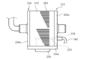
- the configuration in which the negative pressure chamber is provided has been described, but a plurality of communication passages are formed in the moving body, and a predetermined communication passage is communicated with the degassing port depending on the relative position of the moving body. It is also possible to adopt a configuration in which the air port and the desired suction port are communicated with each other. Specifically, the configurations shown in FIGS. 10 and 11 can be adopted.
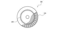
- the suction holding device 233 of FIGS. 10 and 11 has a suction tool 234 including a collet portion 239 in which a plurality of suction ports (not shown) are formed. The plurality of suction ports are provided so as to penetrate the collet portion 239 in the vertical direction (vertical direction in FIG. 10).
- the displacement body for selectively changing the communication state between the suction port and the degassing port 236 according to the relative position with the suction tool 234 is composed of a rotating body 242 that can rotate with respect to the collet portion 239. ..
- the rotating body 242 has a plurality of communication holes 235 formed along the rotation axis direction capable of communicating with the degassing port 236 at a predetermined rotation angle, and communication holes 235 formed from the outer surface to the communication holes 235, respectively, parallel to the rotation axis. Moreover, it has a plurality of elongated holes 243 having different lengths.
- the suction tool 234 has a pair of support portions 234a that rotatably support the columnar rotating body 242 from both sides, and the pair of support portions. It has a connecting portion 234b that connects 234a, and a collet portion 239 is attached to the connecting portion 234b. Further, a degassing port 236 is formed in one of the support portions 234a, and the degassing port 236 is connected to the suction hose 240.
- the communication hole 235 communicating with the degassing port 236 is changed by the relative rotation of the rotating body 243, and the elongated hole 243 communicating with the communication hole 235 communicating with the degassing port 236 becomes a negative pressure, and the collet Suction can be performed by the intake port communicating with the elongated hole 243 which has become the negative pressure among the plurality of intake ports of the unit 239.
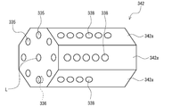
- the shape is not limited to a cylindrical shape or a columnar shape, and for example, as shown in FIG. Good.
- the rotating body 342, which is a moving body shown in FIG. 12, is provided in a polygonal columnar shape, and the rotating body 342 has a plurality of communication holes 335 formed along the rotation axis direction so as to be able to communicate with the degassing port 336 at a predetermined rotation angle. Is formed. Further, one or a plurality of suction ports 338 are formed on each side surface 342a of the rotating body 342, and the suction ports 338 on the same side surface 342a communicate with each other through the same communication hole 335.
- the number of suction ports 338 on each side surface 342a is different, so that it is possible to cope with a change in the number of electronic articles to be sucked.
- the size of the drawings is exaggerated for easy understanding.
- the size of the communication hole 335 varies depending on the electronic component, but when holding the IC chip, a very small hole is preferable.
- FIG. 12 also exaggerates the width of each side surface 342a.
- the suction holding device 33 sucks the electronic parts in only one row, but the suction holding device may suck the electronic parts in a plurality of rows. Further, in the above embodiment, the case where the suction holding device 33 sucks only one row of electronic parts C in one first transfer step in which the electronic parts are transferred from the mounting table 1 to the alignment unit 10 and placed. As described above, the present invention is not limited to this, and it is also possible to adsorb and transport a plurality of rows of electronic components in one first transport step. In this case, when the electronic components are placed on the alignment portion, they may be arranged one row at a time so as to have a space between the rows.
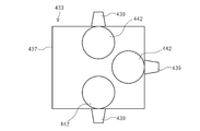
- the suction holding device 433 has a plurality of rotating bodies 442 and a plurality of collet portions 439. Since the rotating body 442 and the collet portion 439 have the same configuration as the moving body 42 and the collet portion 439 of the above embodiment, detailed description thereof will be omitted.
- FIG. 13 is schematically shown, three rotating bodies 442 are built in a negative pressure chamber (not shown) in the housing 437, and a plurality of suction ports (not shown) are provided on three side surfaces of the housing 437. The formed collet portion 439 is attached.
- the housing 437 is rotatable about a rotation axis extending in a direction orthogonal to the paper surface of FIG. 13.
- the electronic article can be adsorbed only by the suction port of each collet portion 439 selected by the rotation of the housing 437.
- the number of electronic components to be adsorbed is changed by the rotation of the rotating body 442.
- the housing 437 rotates so that each side surface faces downward, so that the electronic component adsorbed by each collet portion 439 can be delivered to the aligning portion.
- the suction holding mechanism 33 that picks up and takes out the electronic component by sucking it with a negative pressure is adopted, but the present invention is not limited to this, and the present invention is not limited to this. Any configuration may be used as long as a plurality of electronic components included in the electronic component group are taken out from the mounting table on which the electronic component group is mounted, apart from the electronic component group on the mounting table. For example, a configuration may be adopted in which electronic components arranged in a plurality of rows and a plurality of columns are taken out one column at a time by a conveyor or the like, or moved by a blade or the like to be taken out.
- the transfer direction of the first transfer mechanism 30 and the transfer direction of the second transfer mechanism 50 are substantially orthogonal to each other, but the present invention is not limited to this, and the transfer direction is not limited to this, depending on the device installation environment and the like. Both transfer directions may be the same direction, and may intersect in a state where they are not substantially orthogonal directions.
- one alignment unit may have a plurality of mounting tables or a plurality of first transfer mechanisms, or one mounting table may have a plurality of alignment units. ..
- an example of attaching an IC chip to an RFID tag antenna as an adherend as an electronic component has been described as an example, but in addition, an IC chip is attached to an RFID strap having an IC chip and a magnifying electrode.
- the electronic component attachment device of the present invention is used for attaching an RFID strap to an RFID tag, attaching an electronic component to an IoT board, attaching an electronic component to a sensor board, attaching an LED to an electronic device, and the like. It can be used for mounting and assembling electronic components.
- the defect of the IC chip C is not considered, but in the present invention, it is conceivable to add a configuration for detecting and removing the defective product when the electronic component contains a defective product. Be done.
- the operation is as follows. While the electronic components are transported from the mounting table to the mounting table for temporary storage, the electronic components are inspected for good quality. For example, when an electronic component is a printed electronics product such as an IC chip, an LED substrate, or an IoT substrate, it is judged whether there is a defect in appearance based on an image captured by a camera, and the electric component is energized in terms of function. Judge if there is any defect in.
- an electronic component is a printed electronics product such as an IC chip, an LED substrate, or an IoT substrate.
- the detection of defective products and the removal of defective products may be performed at any timing, but it is particularly preferable in the upstream process because the loss of other parts is reduced.
- the configuration in which the semiconductor wafer is cut and separated into individual IC chips and attached to the RFID tag has been described.
- a defective product is inspected and only a non-defective product is placed. It may be configured to be attached to the RFID tag from a place.
- the electronic component may be a printed electronic product such as an LED substrate or an IoT substrate, in addition to an IC chip.
- the present invention is not limited to this.
- a plurality of electronic components may be placed without being aligned on the mounting table, or may be placed separately in a plurality of rows.
- the mounting table 1 and the alignment unit 10 are used as separate tables, but these may be integrated.
- the electronic components are closely aligned on the mounting table without any gaps, but the electronic components of the present invention are also aligned on the mounting table with gaps.
- the component mounting device can be effectively used. That is, in the present invention, the electronic components closely aligned on the mounting table are arranged by the first transfer mechanism in the alignment section so as to have a space between the columns, and thereafter, a plurality of electronic components in the same row are arranged. Can be attached to the adherend at the same time, and can be effectively applied as long as the spacing between the electronic components arranged on the mounting table is not the same as the spacing between the attachment positions of the plurality of electronic components in the adherend.
- two intervals D1 and D2 having different attachment position intervals are applied to an adherend that is repeated in the row direction, but as shown in FIG. 15, the attachment position intervals are different. It is also applicable to an adherend in which three intervals D3, D4, and D5 are repeated in the row direction, and an adherend in which different intervals are not repeated in the row direction (an adherend having an irregular pattern of attachment positions). For example, it can be applied to all the adherends having different intervals).
- the antenna sheet on which the RFID tag is formed as the adherend has been described as an example, but it can be applied to the case where the electronic components are simultaneously attached to different adherends regardless of the type of the adherend.
- the one having one alignment portion has been described, but the one having a plurality of alignment portions can also be adopted. Further, when a plurality of alignment portions are provided, it is possible to make the alignment pattern different in each alignment portion. Specifically, for example, the odd-numbered columns may be used as the first interval pattern, and the even-numbered columns may be used as the second interval pattern (interval pattern different from the first interval pattern).
- the second transfer mechanism repeatedly transfers the electronic components in the same interval pattern, but the second transfer mechanism can also transfer the electronic components in different interval patterns. Specifically, it is also possible to repeat the step in which the second transfer mechanism transfers the electronic components in the first interval pattern and the step in which the electronic components are transferred in the second interval pattern.
- the second transfer mechanism can repeat the step of transferring the IC chip in the row L1 and the step of transferring the IC chip in the row L2.
- the transfer process may include a step of mounting the electronic components in a first spacing pattern and a step of mounting the electronic components in a second spacing pattern different from the first spacing pattern.
- the second transfer mechanism transfers one line of electronic components in one transfer operation, but it is also possible to have a structure in which the second transfer mechanism transfers a plurality of lines of electronic components at the same time. .. In this case, it is possible that the spacing patterns of the electronic components in a plurality of lines are different from each other. For example, the IC chip in the row L1 and the IC chip in the row L2 in FIG. 15 may be transferred at the same time.
- a plurality of electronic components J, K, M for example, semiconductors and sensors can be aligned and conveyed at the same time. In this case, a plurality of types of electronic components can be efficiently attached.
- each row of electronic components is arranged in an orderly manner in the alignment section.
- electronic components are arranged in a matrix in the alignment section, and electronic components in different columns are spaced apart in the row direction. It is also possible to take out (for example, take out the electronic parts in the first row, the fourth row, and the eighth row). Instead of taking out all the rows of electronic components, it is also possible to take out the electronic components at the positions corresponding to the positions of the adherends.
- the configuration for confirming the position of the adherend is used, but the present invention is not limited to this, and the configuration for confirming the position of the adherend may not be used. Further, the position of the adherend may be confirmed by a mechanism for confirming the position of the adherend, and the position of the electronic component on the mounting table may be adjusted. This position adjustment may be performed by the first transfer mechanism, or another position adjustment mechanism may be provided.
- an electrode sheet on which a pair of electrodes Sa and Sb are formed can also be used.
- the pair of electrodes Sa and Sb are each formed to have a predetermined width along the longitudinal direction.
- the pair of electrodes Sa and Sb are arranged side by side in the width direction with a gap formed in the center in the width direction interposed therebetween.
- the width of the pair of electrodes is the same, but may be different.
- the strap manufacturing device in FIG. 17 manufactures straps used for RFID tags and the like.
- the strap includes a pair of electrodes Sa and Sb arranged with a gap, and an IC chip C in contact with the pair of electrodes Sa and Sb and arranged in the gap between the pair of electrodes Sa and Sb. is there.
- the strap manufacturing apparatus includes an alignment case 10, an object transfer mechanism (not shown (the mechanism having the same function as the sheet transfer mechanism 2 in FIG. 1)), and an IC chip transfer mechanism (not shown (second transfer mechanism in FIG. 1)). 50 and a mechanism of the same type as the mounting transfer mechanism 80)).
- a semiconductor wafer is cut using a laser or the like to form a plurality of IC chips C, and then the plurality of IC chips C are arranged in a plurality of rows at intervals.
- the alignment case 10 is formed so that row-shaped grooves 10A are lined up, and a plurality of IC chips C are arranged in the grooves.
- the front row IC chip C in the groove 10A of the alignment case 10 moves, the remaining row of IC chips C moves forward by one IC chip C.
- the plurality of IC chip rows may all be arranged at the same predetermined interval, or may be arranged at different intervals.
- the intervals of the plurality of IC chip rows may be the same, or may be different.
- the plurality of IC chip rows may be arranged according to the interval of the object to be attached, or may be arranged at a predetermined interval.
- the mounting object transport mechanism transports the mounting target and moves the portion on which the IC chip is not mounted to the mounting position.
- the mounted object transport mechanism moves the place where the IC chip is mounted from the mounting position.
- the IC chip transport mechanism transports the IC chip C in the front row among the plurality of IC chip rows aligned in the alignment case 10A to the gap between a pair of electrodes in row units and places them.
- the IC chip transport mechanism transports the IC chips in the front row while maintaining the distance interval.
- the method of manufacturing a strap by the apparatus of FIG. 17 includes a step of transporting an electrode sheet on which a pair of electrodes are formed at a predetermined position with a predetermined gap along the longitudinal direction, and a plurality of IC chips as shown in FIG. 17A.
- the plurality of IC chips C are conveyed to the predetermined positions while being held in a row state, and as shown in FIG. 17B, they come into contact with a pair of electrodes Sa and Sb and are paired.
- a step of placing the IC chip in the gap between the electrodes Sa and Sb of the above is provided.
- the strap raw fabric in which the straps are connected can be manufactured by the alignment case 10A, the object to be mounted transport mechanism, and the IC chip transport mechanism, but even if the device is further provided with a cutting mechanism. good. That is, the method for manufacturing the strap can further include a step of cutting each strap as shown in FIG. 17C after the step of mounting the IC chip.
- the cutting device manufactures each strap by performing a cutting operation between successive IC chips. In addition to using a cutting tool for cutting, any laser, half-cut, or any other structure that can cut at least a part of the object to be mounted can be used.
- the strap manufacturing device is further equipped with a coating device for applying an adhesive or the like to the strap.
- a coating device for applying an adhesive or the like to the strap.
- a release paper supply mechanism for attaching the release paper to the surface to which the adhesive is applied.
- the spacing between the rows of the IC chips C is determined. Therefore, if the spacing between the rows of the IC chips C is to be changed to different spacing, different alignment cases are prepared. There is a need. In the device of FIG. 17, since the spacing between the mounted objects such as the IC chip C can be changed by changing the alignment case, it is possible to easily deal with various types of mounted objects having different mounting intervals.
- the configuration of the strap in FIG. 17 a configuration in which a pair of electrodes 17a and 17b are arranged on both sides in the width direction of the gap with a gap along the longitudinal direction of the original fabric is adopted, as shown in FIG.
- the pair of electrodes 17a and 17b may have a tapered shape toward the gap between the pair of electrodes.
- the gap between the pair of electrodes 17a and 17b is constantly provided as in the strap of FIG. 17, and the mounting accuracy in the longitudinal direction of the original fabric may be low. In other words, it is easy to attach because it is only necessary to attach the attached object accurately even at the position in the width direction. Therefore, the strap can be manufactured efficiently.
- the electronic component mounting device of the present invention can mount the electronic component on the adherend accurately and efficiently as described above, it can be suitably used, for example, when the IC chip of the semiconductor wafer is mounted on the antenna member. ..
Landscapes
- Engineering & Computer Science (AREA)
- Manufacturing & Machinery (AREA)
- Microelectronics & Electronic Packaging (AREA)
- Supply And Installment Of Electrical Components (AREA)
- Wire Bonding (AREA)
Abstract
Description
所定箇所に載置された複数の電子部品を異なる間隔で被着物に取り付ける電子部品取付装置であって、
上記所定箇所に載置された上記複数の電子部品から一部の複数の上記電子部品を取り出す取り出し機構と、
上記取り出し機構が取り出した上記電子部品を搬送し、上記被着物に到達する前に上記複数の電子部品が上記被着物へ取り付ける上記異なる間隔となるよう各上記電子部品を移動させ、上記電子部品を上記被着物まで搬送する搬送機構と、
上記搬送機構が搬送した電子部品を上記被着物の所定位置に取り付ける取付移送機構と、
を備える。
所定箇所に載置された複数の電子部品を異なる間隔で被着物に取り付ける電子装置の製造方法であって、
上記所定箇所に載置された上記複数の電子部品から一部の複数の上記電子部品を取り出す取り出し工程と、
上記取り出し工程で取り出された上記電子部品を搬送し、上記被着物に到達する前に上記複数の電子部品が上記被着物へ取り付ける上記異なる間隔となるよう各上記電子部品を移動させ、上記電子部品を上記被着物まで搬送する搬送工程と、
上記搬送工程にて搬送された電子部品を上記被着物の所定位置に取り付ける取付移送工程と、
を備える。
複数の電子部品を異なる間隔で被着物に同時に取り付ける電子装置の製造方法であって、
所定箇所から複数の電子部品を取り出し保持する取り出し工程と、
上記取り出し工程で取り出された複数の上記電子部品を整列部まで搬送し、整列部に上記電子部品を載置する第一搬送工程と、
上記整列部に載置された上記電子部品を保持しつつ上記被着物まで搬送する第二搬送工程と、
上記第二搬送工程で搬送された上記電子部品を上記被着物の所定位置に取り付ける取付移送工程と、
を備える。
複数の電子部品を異なる間隔で被着物に同時に取り付ける電子装置の製造方法であって、
所定箇所から複数の電子部品を取り出す取り出し工程と、
上記取り出し工程で取り出された複数の上記電子部品を、上記複数の電子部品が上記被着物へ取り付ける上記異なる間隔で搬送機構に並べて保持させる保持工程と、
上記搬送機構に上記電子部品を保持させた状態で上記被着物まで搬送する搬送工程と、
上記搬送工程で搬送された上記電子部品を上記被着物の所定位置に取り付ける取付移送工程と、
を備える。
RFID装置に用いられるストラップを製造する方法であって、
長手方向に沿って所定の隙間をあけて一対の電極が形成された電極シートを所定位置に搬送する工程と、
複数のICチップが間隔をあけて複数列で並べられる工程と、
上記複数のICチップを列状態で保持しながら上記所定位置まで搬送し、上記一対の電極に接触し且つ上記一対の電極の上記隙間に上記複数のICチップを載置する工程と、
を備える。
図1から図6に本発明の一実施形態に係る電子部品取付装置100の全体又は一部を示す。電子部品取付装置100は、所定箇所に載置された複数の電子部品を異なる間隔で被着物に取り付ける電子部品取付装置である。電子部品取付装置100は、複数列かつ複数行に整列された状態で多数の電子部品Cが密接して配置された状態において、電子部品を取り出し、その電子部品(ここではICチップC)を被着物(本実施形態においてはRFIDタグA)に取り付ける装置である。ここで、「行」と「列」は、それぞれ図1におけるX方向への配列とY方向への配列を意味する。以下、電子部品の一例としてICチップを例にとり説明する。ICチップCは、例えば多数の回路パターンが形成された薄板円盤状の半導体ウエハWが格子状に切断されて形成されている。電子部品取付装置100は、隙間なく複数列かつ複数行に整列された多数のICチップCから複数のICチップCを列状で取り出し、それらのICチップCのそれぞれをRFIDタグAに取り付ける装置である。なお、各図は模式的図面であり、各部材のサイズ、個数等を模式的に示すものである。
当該電子部品取付装置100は、半導体ウエハWが載置される載置台1と、被着物であるRFIDタグAのシートを搬送するシート搬送機構2と、載置台1からシート搬送機構2まで電子部品であるICチップCを搬送する部品搬送機構3と、部品搬送機構3によって搬送されたICチップCをRFIDタグAに取り付け移送する取付移送機構80とを有している。また、電子部品取付装置100は、各部材の動作を制御する制御部100Aを有している。
載置台1は、上述のように半導体ウエハWがレーザー等で切断され、隙間なく複数列かつ複数行に整列されたICチップCに個片化された状態で載置される。また、載置台1は、載置されたICチップCの整列方向を調整する調整手段を有している。具体的には、載置台1は、載置された半導体ウエハWを撮像する撮像部(図示省略)と、電子部品Cの整列方向が正しくない場合(図1のXY方向に合致していない場合)に、載置台1の中心を通り図1の紙面に直交する方向に伸びる回転軸を中心として半導体ウエハWを回転する回転部(図示省略)とを有している。
部品搬送機構3は、複数のICチップCをピックアップして取り出す取り出し機構としての吸着保持装置33と、吸着保持装置33が取り出したICチップCを搬送し、RFIDタグAに到達する前に隣り合うICチップCの間隔が上記異なる間隔(複数のICチップCがRFIDタグAへ取り付けられる間隔)となるよう各ICチップCを移動させ、ICチップCをRFIDタグAまで搬送する部品搬送機構3とを備えている。具体的には、部品搬送機構3は、載置台1及びシート搬送機構2の間でICチップCが仮置きされる整列部としての載置テーブル10と、載置台1から載置テーブル10までICチップCを移送する第一移送機構30と、載置テーブル10からRFIDタグAまでICチップCを移送する第二移送機構50とを有する。部品搬送機構3は、載置台1上のICチップCを、まず載置テーブル10まで第一移送機構30によって移動させて載置テーブル10に仮置きし、この載置テーブル10上のICチップCを第二移送機構50によってRFIDタグAのアンテナまで搬送する。本実施形態においては、第一移送機構30は第一方向(図1のX方向)にICチップCを移送し、第二移送機構50は第一方向に直交する第二方向(図1のY方向)にICチップCを移送する。
載置テーブル10は、上述のように第一移送機構30からICチップCを受け取り、第二移送機構50によってICチップCが受け取られる。この載置テーブル10は、第二移送機構50に接近及び離反するようスライド移動する。つまり、載置テーブル10は、第二移送機構50から離反して第一移送機構30とICチップCを受け渡す第一受渡位置P1と、第二移送機構50に接近して第二移送機構50とICチップCを受け渡す第二受渡位置P2とを移動する。なお、載置テーブル10は、第一受渡位置P1と第二受渡位置P2との間に配された図示省略のレールにスライド可能に支持されている。
第一移送機構30は、1列に並んだ8個のICチップCを同時に載置台1から取り出し、載置テーブル10に移動する。第一移送機構30は、水平方向(図1及び図2のX方向及びY方向)並びに上下方向(図1の紙面に直交する方向)に移動可能な吸着保持装置33を有している(図2参照)。また、第一移送機構30は、図2に示すように、柱部30aと、走行体31と、上下動体32とを有している。柱部30aは、第一移送機構30の移送方向に沿ってレールが配される。走行体31は、柱部30aに沿って走行する。上下動体32は、走行体31に上下動可能に支持されると共に吸着保持装置33を第一移送機構30の搬送方向に対する垂直方向(図1及び図2のY方向)に移動可能に支持する。
吸着保持装置33は、上述のように載置台1から1列に並んだ複数個のICチップCを吸着保持することができる。吸着保持装置33は、吸着するICチップCの個数を変更可能である。この吸着保持装置33は、図3~図6に示すように、脱気口36(図4参照)が形成された吸引具34と、この吸引具34に対して相対的に変位(回転)する変位体42とを備えている。脱気口36に連通することで吸着口38(図4及び図5参照)は吸引力を発揮する。変位体42は、吸引具34との相対位置によって複数の吸着口38と脱気口36との連通状態を選択的に変更可能に設けられている。
第二移送機構50は、図2に示すように、取出機構60と、仮置部70とを有する。図1及び図2を参照して、取付機構60は、整列部10から同一行6個のICチップCを同時に吸着して取り出す。仮置部70は、同一行6個のICチップCが受け渡される。つまり、第二移送機構50は、整列部10上から同一行6個のICチップCを取出手段60によって取り出して、この取り出されたICチップCを一度仮置部70に仮置きし、そして、この仮置部70上のICチップCを、アンテナシートSまで搬送するものである。
取付移送機構80は、RFIDタグA上を上下動可能な保有部81と、この保有部81を上下動可能に支持する移動部材82とを有している。取付移送機構80は、部品搬送機構3によってRFIDタグAが形成されたアンテナシートSまで搬送されたICチップCをRFIDタグAの所定位置に取り付ける。この移動部材82は、レール51に沿って水平方向(図1及び図2のY方向)に移動可能に支持されている。取付移送機構80は、実装位置P4においてICチップCをRFIDタグAに取り付ける。
図1を参照して、シート搬送機構2は、上述のようにICチップCを取り付けるRFIDタグAが形成されたアンテナシートSを搬送する機構である。本実施形態においては、シート搬送機構2は、多数のRFIDタグAが形成されたアンテナシートSを搬送している。シート搬送機構2は、取付移送機構80が吸着保持する複数のICチップCの整列方向(整列部10における行形成方向(図1のX方向))に沿ってアンテナシートSを搬送する。
電子部品取付装置100は、ICチップCを取り付けられる前においてアンテナシートS(複数のRFIDタグA)の位置を確認する被着物位置確認部材100Bを備える。被着物位置確認部材100Bは、カメラから構成されている。被着物位置確認部材100Bは、シート搬送機構2によって搬送されるアンテナシートSを実装位置P4よりも上流側で撮像する。被着物位置確認部材100Bは、制御部100Aに接続され、電子部品取付装置100は、被着物位置確認部材100Bにより確認されたRFIDタグAの位置に基づいてRFIDタグA同士の間隔を算出し、この算出した間隔に基づいてICチップCを取り付けることができる。
次に、本発明の一実施形態に係る電子装置の製造方法について説明する。この電子装置の製造方法は、上記構成からなる電子部品取付装置100を用い、ICチップCを取り付ける。
第一搬送工程では、載置台1から8個のICチップCが同時に吸着され、吸着されたICチップCが載置テーブル10に移送され、載置テーブル10に受け渡される。この第一搬送工程が繰り返し行われることで、載置テーブル10には列間が上記異なる間隔D1,D2を有する状態で複数のICチップCの列が並べられる。
第二搬送工程は、整列部10から1行複数個(本実施形態では6個)のICチップCを取出機構60が取出す工程と、この取出機構60が取り出したICチップCを反転機構90が反転する工程と、反転機構90が反転したICチップCを仮置部70に載置する工程と、仮置部70に載置された1行8個のICチップCを受取搬送機構75及び取付移送機構80がRFIDタグAまで移送しRFIDタグAに載置する工程とを有する。
電子部品取付装置100にあっては、第一移送機構30は、載置台1から複数個(本実施形態では8個)のICチップCを同時に吸着することで取り出し、第二移送機構50は、載置テーブル10から、列間に間隔を有する状態の同一行複数個(本実施形態では6個)のICチップCを同時に吸着することで取り出し、この同一行6個のICチップCをRFIDタグAに同時に載置する。このように電子部品取付装置100は、複数のICチップCを同時にRFIDタグAに載置することができるため、ICチップCの取付を効率的に行うことができる。
本発明は上記実施形態の構成に限定されるものではなく、本発明の意図する範囲内において適宜設計変更可能である。
2 搬送機構
3 移送機構
10 整列部
30 第一移送機構
50 第二移送機構
30a 柱部
31 走行体
32 上下動体
33 吸着保持装置
34 吸引具
35 負圧室
36 脱気口
37 筐体
38 吸着口
39 コレット部
40 吸引ホース
41 軸受部
42 移動体
43 長孔
50 第二移送機構
51 レール
60 取出手段
61 取出手段用吸着保持部
62 取出手段用支持部材
70 仮置部
71 修正手段
80 取付移送機構
81 保有部
82 移動部材
90 反転手段
95 供給装置
96 回収装置
100A 制御部
100B 被着物位置確認部材
C 電子部品
A 被着物
W 半導体ウエハ
S 長尺状シート
P1 第一受渡位置
P2 第二受渡位置
P3 第三受渡位置
P4 実装位置
Claims (29)
- 所定箇所に載置された複数の電子部品を異なる間隔で被着物に取り付ける電子部品取付装置であって、
上記所定箇所に載置された上記複数の電子部品から一部の複数の上記電子部品を取り出す取り出し機構と、
上記取り出し機構が取り出した上記電子部品を搬送し、上記被着物に到達する前に上記複数の電子部品が上記被着物へ取り付ける上記異なる間隔となるよう各上記電子部品を移動させ、上記電子部品を上記被着物まで搬送する搬送機構と、
上記搬送機構が搬送した電子部品を上記被着物の所定位置に取り付ける取付移送機構と、
を備えた電子部品取付装置。 - 上記搬送機構は、
上記取り出し機構と上記取付移送機構との間で、上記電子部品がそれぞれ上記異なる間隔を有する複数の列状に配置される整列部と、
上記取り出し機構が取り出した上記電子部品を保持するとともに、これらの上記電子部品を上記整列部に移動させる第一移送機構と、
上記整列部に移動された上記電子部品を上記取付移送機構まで移送する第二移送機構と、を有する、
請求項1に記載の電子部品取付装置。 - 上記第一移送機構は、上記整列部に上記電子部品が列間に上記異なる間隔を有する状態で複数列並べて移動させて載置し、
上記第二移送機構は、上記整列部から同一行複数個の電子部品を、各上記電子部品の間が上記異なる間隔となった状態を保持して搬送し、
上記取付移送機構は、各上記電子部品の間が上記異なる間隔となった状態で上記被着物上に取り付ける
請求項2に記載の電子部品取付装置。 - 上記第二移送機構が、
上記整列部から同一行複数個の電子部品を同時に吸着することで取り出す取出手段と、
上記取出手段が取り出した同一行複数個の電子部品が受け渡される仮置部と、有し、
上記取付移送機構が、上記仮置部に受け渡された同一行複数個の上記電子部品を吸着すると共に上記被着物に取り付ける請求項2又は請求項3に記載の電子部品取付装置。 - 上記第二移送機構が、上記取出手段から同一行複数個の上記電子部品が載置されると共に、載置された電子部品を反転して上記仮置部に受け渡す反転手段をさらに有する請求項4に記載の電子部品取付装置。
- 上記仮置部が、載置された上記電子部品の位置を修正する修正手段を備える請求項4又は請求項5に記載の電子部品取付装置。
- 上記第二移送機構が、上記整列部から複数行の電子部品を同時に吸着する請求項2から請求項6のいずれか1項に記載の電子部品取付装置。
- 上記第二移送機構が、複数行の上記電子部品を同時に被着物に載置する請求項2から請求項7のいずれか1項に記載の電子部品取付装置。
- 上記整列部が、配置された上記電子部品を、上記第一移送機構と電子部品を受け渡す第一受渡位置と、上記第二移送機構と電子部品を受け渡す第二受渡し位置との間を移動する請求項2から請求項8のいずれか1項に記載の電子部品取付装置。
- 上記第一移送機構が、吸着する電子部品の個数を変更可能な吸着保持装置を備えている請求項2から請求項9のいずれか1項に記載の電子部品取付装置。
- 上記第二移送機構によって保持された複数の上記電子部品の並ぶ方向は、取り付けられる複数の上記被着物が並ぶ方向と平行である請求項2から請求項10のいずれか1項に記載の電子部品取付装置。
- 上記搬送機構は、複数の上記整列部を有しており、それぞれ載置ポジションと取り出しポジションに位置可能である請求項2から請求項11のいずれか1項に記載の電子部品取付装置。
- 上記第二移送機構は、各上記電子部品間の間隔が上記異なる間隔となる状態で搬送する請求項2から請求項12のいずれか1項に記載の電子部品取付装置。
- 上記第二移送機構は、一度の搬送作業に際して複数行の電子部品を搬送し、複数行の電子部品の間隔のパターンが異なる請求項2から請求項13のいずれか1項に記載の電子部品取付装置。
- 上記取り出し機構は、上記複数の電子部品を一列に並んだ状態で取り出す請求項1から請求項14のいずれか1項に記載の電子部品取付装置。
- 上記電子部品は、RFID装置に用いられるICチップ又はICチップが搭載されたストラップである請求項1から請求項15のいずれか1項に記載の電子部品取付装置。
- 複数の上記電子部品は、上記載置台に密接して載置される請求項1から請求項16のいずれか1項に記載の電子部品取付装置。
- 上記取り出し機構は、上記電子部品を吸着保持する請求項1から請求項17のいずれか1項に記載の電子部品取付装置。
- 上記取付移送機構は複数の上記電子部品を同じ高さ位置で上記被着物に取り付ける請求項1から請求項18のいずれか1項に記載の電子部品取付装置。
- 上記電子部品が取り付けられる前において上記被着物の被着位置を確認する被着物位置確認部材をさらに備える請求項1から請求項19のいずれか1項に記載の電子部品取付装置。
- 上記被着位置が行方向に異なる間隔の繰り返しパターンを有する請求項1から請求項20のいずれか1項に記載の電子部品取付装置。
- 上記異なる間隔のパターンが行方向に繰り返されている請求項1から請求項21のいずれか1項に記載の電子部品取付装置。
- 上記異なる間隔のパターンが行方向に繰り返されていない請求項1から請求項22のいずれか1項に記載の電子部品取付装置。
- 所定箇所に載置された複数の電子部品を異なる間隔で被着物に取り付ける電子装置の製造方法であって、
上記所定箇所に載置された上記複数の電子部品から一部の複数の上記電子部品を取り出す取り出し工程と、
上記取り出し工程で取り出された上記電子部品を搬送し、上記被着物に到達する前に上記複数の電子部品が上記被着物へ取り付ける上記異なる間隔となるよう各上記電子部品を移動させ、上記電子部品を上記被着物まで搬送する搬送工程と、
上記搬送工程にて搬送された電子部品を上記被着物の所定位置に取り付ける取付移送工程と、
を備えた電子装置の製造方法。 - 上記搬送工程が、上記電子部品を第一の間隔パターンで取り付けるステップと、上記電子部品を第一の間隔パターンと異なる第二の間隔パターンで取り付けるステップとを有する請求項24に記載の電子部品の製造方法。
- 複数の電子部品を異なる間隔で被着物に同時に取り付ける電子装置の製造方法であって、
所定箇所から複数の電子部品を取り出し保持する取り出し工程と、
上記取り出し工程で取り出された複数の上記電子部品を整列部まで搬送し、整列部に上記電子部品を載置する第一搬送工程と、
上記整列部に載置された上記電子部品を保持しつつ上記被着物まで搬送する第二搬送工程と、
上記第二搬送工程で搬送された上記電子部品を上記被着物の所定位置に取り付ける取付移送工程と、
を備えた電子装置の製造方法。 - 上記第一搬送工程では、上記整列部上に上記第二搬送工程で複数の上記電子部品を列状に並べて搬送できるように上記電子部品を載置する請求項26に記載の電子装置の製造方法。
- 複数の電子部品を異なる間隔で被着物に同時に取り付ける電子装置の製造方法であって、
所定箇所から複数の電子部品を取り出す取り出し工程と、
上記取り出し工程で取り出された複数の上記電子部品を、上記複数の電子部品が上記被着物へ取り付ける上記異なる間隔で搬送機構に並べて保持させる保持工程と、
上記搬送機構に上記電子部品を保持させた状態で上記被着物まで搬送する搬送工程と、
上記搬送工程で搬送された上記電子部品を上記被着物の所定位置に取り付ける取付移送工程と、
を備えた電子装置の製造方法。 - RFID装置に用いられるストラップを製造する方法であって、
長手方向に沿って所定の隙間をあけて一対の電極が形成された電極シートを所定位置に搬送する工程と、
複数のICチップが間隔をあけて複数列で並べられる工程と、
上記複数のICチップを列状態で保持しながら上記所定位置まで搬送し、上記一対の電極に接触し且つ上記一対の電極の上記隙間に上記複数のICチップを載置する工程と、
を備えたストラップの製造方法。
Priority Applications (4)
| Application Number | Priority Date | Filing Date | Title |
|---|---|---|---|
| JP2021520785A JP7575097B2 (ja) | 2019-05-21 | 2020-05-18 | 電子部品取付装置、電子装置の製造方法及びストラップの製造方法 |
| US17/612,933 US12089340B2 (en) | 2019-05-21 | 2020-05-18 | Electronic component mounting device for mounting electronic components at certain intervals |
| CN202080037729.XA CN113874990A (zh) | 2019-05-21 | 2020-05-18 | 电子组件安装装置、电子装置的制造方法及条带的制造方法 |
| EP20809056.3A EP3975227A4 (en) | 2019-05-21 | 2020-05-18 | DEVICE FOR FIXING ELECTRONIC COMPONENTS, METHOD OF MANUFACTURING AN ELECTRONIC DEVICE AND METHOD OF MANUFACTURING A TAPE |
Applications Claiming Priority (2)
| Application Number | Priority Date | Filing Date | Title |
|---|---|---|---|
| JP2019095593 | 2019-05-21 | ||
| JP2019-095593 | 2019-05-21 |
Publications (1)
| Publication Number | Publication Date |
|---|---|
| WO2020235535A1 true WO2020235535A1 (ja) | 2020-11-26 |
Family
ID=73459407
Family Applications (1)
| Application Number | Title | Priority Date | Filing Date |
|---|---|---|---|
| PCT/JP2020/019679 Ceased WO2020235535A1 (ja) | 2019-05-21 | 2020-05-18 | 電子部品取付装置、電子装置の製造方法及びストラップの製造方法 |
Country Status (6)
| Country | Link |
|---|---|
| US (1) | US12089340B2 (ja) |
| EP (1) | EP3975227A4 (ja) |
| JP (1) | JP7575097B2 (ja) |
| CN (1) | CN113874990A (ja) |
| TW (1) | TW202106155A (ja) |
| WO (1) | WO2020235535A1 (ja) |
Cited By (1)
| Publication number | Priority date | Publication date | Assignee | Title |
|---|---|---|---|---|
| CN113451187A (zh) * | 2021-06-24 | 2021-09-28 | 深圳市创一智能装备有限公司 | 硅片的输送装置 |
Families Citing this family (1)
| Publication number | Priority date | Publication date | Assignee | Title |
|---|---|---|---|---|
| CN119174300A (zh) * | 2022-07-26 | 2024-12-20 | 雅马哈发动机株式会社 | 表面安装机和表面安装方法 |
Citations (4)
| Publication number | Priority date | Publication date | Assignee | Title |
|---|---|---|---|---|
| JPS5636196A (en) * | 1979-09-03 | 1981-04-09 | Sony Corp | Apparatus for assembling electronic device circuit |
| JP2006173190A (ja) | 2004-12-13 | 2006-06-29 | Hitachi Chem Co Ltd | 半導体装置の製造方法及びicチップ配列用支持材 |
| WO2010032427A1 (ja) * | 2008-09-19 | 2010-03-25 | パナソニック株式会社 | 部品実装装置及び部品実装方法 |
| WO2016125245A1 (ja) * | 2015-02-03 | 2016-08-11 | 富士機械製造株式会社 | 供給部品移載装置 |
Family Cites Families (11)
| Publication number | Priority date | Publication date | Assignee | Title |
|---|---|---|---|---|
| US6631557B2 (en) * | 2000-01-31 | 2003-10-14 | Shibaura Mechatronics Corporation | Method and apparatus for mounting electronic device |
| JP3636127B2 (ja) | 2001-10-12 | 2005-04-06 | 松下電器産業株式会社 | 電子部品実装装置および電子部品実装方法 |
| JP4810531B2 (ja) | 2005-04-06 | 2011-11-09 | 株式会社 ハリーズ | 電子部品の製造装置 |
| CN101341587B (zh) | 2005-12-22 | 2010-10-27 | 芝浦机械电子株式会社 | 电子部件的安装装置及安装方法 |
| DE102006051607B4 (de) | 2006-11-02 | 2008-11-20 | Mühlbauer Ag | Verfahren und Vorrichtung zum serienmäßigen Aufbringen und Befestigen von elektronischen Bauteilen auf Substraten |
| KR101639667B1 (ko) | 2010-08-10 | 2016-07-14 | 한화테크윈 주식회사 | 부품 실장기 |
| KR101649855B1 (ko) | 2010-11-12 | 2016-08-23 | 한화테크윈 주식회사 | 가변 피치 헤드를 이용한 부품 실장 최적화 방법 및 그 방법을 이용한 부품 실장기 |
| JP2015157348A (ja) * | 2014-01-21 | 2015-09-03 | ソニー株式会社 | 保持ヘッド、搬送装置、搬送方法、実装装置、実装方法、及び電子機器 |
| WO2016032427A1 (en) * | 2014-08-25 | 2016-03-03 | SoliDDD Corp. | Three-dimensional video production system |
| JP2018060993A (ja) * | 2016-09-29 | 2018-04-12 | 東レエンジニアリング株式会社 | 転写方法、実装方法、転写装置、及び実装装置 |
| JP7297673B2 (ja) * | 2017-11-21 | 2023-06-26 | 株式会社ジャルコ | 電子部品取付装置及び電子装置の製造方法 |
-
2020
- 2020-05-18 US US17/612,933 patent/US12089340B2/en active Active
- 2020-05-18 WO PCT/JP2020/019679 patent/WO2020235535A1/ja not_active Ceased
- 2020-05-18 CN CN202080037729.XA patent/CN113874990A/zh active Pending
- 2020-05-18 EP EP20809056.3A patent/EP3975227A4/en not_active Withdrawn
- 2020-05-18 JP JP2021520785A patent/JP7575097B2/ja active Active
- 2020-05-21 TW TW109116932A patent/TW202106155A/zh unknown
Patent Citations (4)
| Publication number | Priority date | Publication date | Assignee | Title |
|---|---|---|---|---|
| JPS5636196A (en) * | 1979-09-03 | 1981-04-09 | Sony Corp | Apparatus for assembling electronic device circuit |
| JP2006173190A (ja) | 2004-12-13 | 2006-06-29 | Hitachi Chem Co Ltd | 半導体装置の製造方法及びicチップ配列用支持材 |
| WO2010032427A1 (ja) * | 2008-09-19 | 2010-03-25 | パナソニック株式会社 | 部品実装装置及び部品実装方法 |
| WO2016125245A1 (ja) * | 2015-02-03 | 2016-08-11 | 富士機械製造株式会社 | 供給部品移載装置 |
Non-Patent Citations (1)
| Title |
|---|
| See also references of EP3975227A4 |
Cited By (1)
| Publication number | Priority date | Publication date | Assignee | Title |
|---|---|---|---|---|
| CN113451187A (zh) * | 2021-06-24 | 2021-09-28 | 深圳市创一智能装备有限公司 | 硅片的输送装置 |
Also Published As
| Publication number | Publication date |
|---|---|
| JPWO2020235535A1 (ja) | 2020-11-26 |
| CN113874990A (zh) | 2021-12-31 |
| US20220232745A1 (en) | 2022-07-21 |
| JP7575097B2 (ja) | 2024-10-29 |
| TW202106155A (zh) | 2021-02-01 |
| EP3975227A1 (en) | 2022-03-30 |
| US12089340B2 (en) | 2024-09-10 |
| EP3975227A4 (en) | 2023-07-05 |
Similar Documents
| Publication | Publication Date | Title |
|---|---|---|
| JP7297673B2 (ja) | 電子部品取付装置及び電子装置の製造方法 | |
| JP4905979B2 (ja) | 包装機への袋供給方法及び装置 | |
| TWI673806B (zh) | 熱壓鍵合裝置 | |
| CN114284170B (zh) | 用于将多个芯片贴片到载板的芯片贴片装置和方法 | |
| KR102158024B1 (ko) | 절단 장치, 반도체 패키지의 부착 방법 및 전자 부품의 제조 방법 | |
| CN106981444B (zh) | 热压键合装置 | |
| JP5035843B2 (ja) | 半導体処理装置 | |
| KR20170006343A (ko) | 플립칩 본딩 장치 및 방법 | |
| WO2020235535A1 (ja) | 電子部品取付装置、電子装置の製造方法及びストラップの製造方法 | |
| WO2013171863A1 (ja) | ダイボンダー装置 | |
| JP3304295B2 (ja) | ダイボンダ | |
| JP2004182293A (ja) | 半導体装置のテーピング装置 | |
| US10661401B2 (en) | Component mounted body manufacturing system and component mounted body manufacturing method | |
| CN101340809B (zh) | 自动装配机以及用于处理元器件的方法 | |
| JP2004121990A (ja) | ワーク搬送収納装置及びワーク搬送収納方法 | |
| WO2007083360A1 (ja) | 半導体製造装置及び製造方法 | |
| JP2019192820A (ja) | ワーク処理装置及びボール搭載装置 | |
| JP4165927B2 (ja) | 部品の移載装置 | |
| JP2010245479A (ja) | 半導体チップ搭載装置 | |
| JP2019096703A (ja) | 吸着保持装置 | |
| JP5405267B2 (ja) | 電子部品搬送装置 | |
| JP2001150255A (ja) | 部品供給装置 | |
| TWI919848B (zh) | 用於將多個晶粒貼片到載板的晶粒黏貼裝置和方法 | |
| WO2019171564A1 (ja) | 部品実装装置、部品実装システムおよび部品実装方法 | |
| TW202541219A (zh) | 用於將多個晶粒貼片到載板的晶粒黏貼裝置和方法 |
Legal Events
| Date | Code | Title | Description |
|---|---|---|---|
| 121 | Ep: the epo has been informed by wipo that ep was designated in this application |
Ref document number: 20809056 Country of ref document: EP Kind code of ref document: A1 |
|
| ENP | Entry into the national phase |
Ref document number: 2021520785 Country of ref document: JP Kind code of ref document: A |
|
| NENP | Non-entry into the national phase |
Ref country code: DE |
|
| ENP | Entry into the national phase |
Ref document number: 2020809056 Country of ref document: EP Effective date: 20211221 |
|
| WWW | Wipo information: withdrawn in national office |
Ref document number: 2020809056 Country of ref document: EP |