WO2021006061A1 - 放射線位置検出器 - Google Patents
放射線位置検出器 Download PDFInfo
- Publication number
- WO2021006061A1 WO2021006061A1 PCT/JP2020/025134 JP2020025134W WO2021006061A1 WO 2021006061 A1 WO2021006061 A1 WO 2021006061A1 JP 2020025134 W JP2020025134 W JP 2020025134W WO 2021006061 A1 WO2021006061 A1 WO 2021006061A1
- Authority
- WO
- WIPO (PCT)
- Prior art keywords
- scintillator
- unit
- light receiving
- receiving element
- array
- Prior art date
- Legal status (The legal status is an assumption and is not a legal conclusion. Google has not performed a legal analysis and makes no representation as to the accuracy of the status listed.)
- Ceased
Links
Images


Classifications
-
- G—PHYSICS
- G01—MEASURING; TESTING
- G01T—MEASUREMENT OF NUCLEAR OR X-RADIATION
- G01T1/00—Measuring X-radiation, gamma radiation, corpuscular radiation, or cosmic radiation
- G01T1/16—Measuring radiation intensity
- G01T1/161—Applications in the field of nuclear medicine, e.g. in vivo counting
- G01T1/164—Scintigraphy
- G01T1/1641—Static instruments for imaging the distribution of radioactivity in one or two dimensions using one or several scintillating elements; Radio-isotope cameras
- G01T1/1642—Static instruments for imaging the distribution of radioactivity in one or two dimensions using one or several scintillating elements; Radio-isotope cameras using a scintillation crystal and position sensing photodetector arrays, e.g. ANGER cameras
-
- G—PHYSICS
- G01—MEASURING; TESTING
- G01T—MEASUREMENT OF NUCLEAR OR X-RADIATION
- G01T1/00—Measuring X-radiation, gamma radiation, corpuscular radiation, or cosmic radiation
- G01T1/16—Measuring radiation intensity
- G01T1/161—Applications in the field of nuclear medicine, e.g. in vivo counting
- G01T1/164—Scintigraphy
- G01T1/1641—Static instruments for imaging the distribution of radioactivity in one or two dimensions using one or several scintillating elements; Radio-isotope cameras
- G01T1/1644—Static instruments for imaging the distribution of radioactivity in one or two dimensions using one or several scintillating elements; Radio-isotope cameras using an array of optically separate scintillation elements permitting direct location of scintillations
-
- G—PHYSICS
- G01—MEASURING; TESTING
- G01T—MEASUREMENT OF NUCLEAR OR X-RADIATION
- G01T1/00—Measuring X-radiation, gamma radiation, corpuscular radiation, or cosmic radiation
- G01T1/16—Measuring radiation intensity
- G01T1/20—Measuring radiation intensity with scintillation detectors
- G01T1/2002—Optical details, e.g. reflecting or diffusing layers
-
- G—PHYSICS
- G01—MEASURING; TESTING
- G01T—MEASUREMENT OF NUCLEAR OR X-RADIATION
- G01T1/00—Measuring X-radiation, gamma radiation, corpuscular radiation, or cosmic radiation
- G01T1/29—Measurement performed on radiation beams, e.g. position or section of the beam; Measurement of spatial distribution of radiation
- G01T1/2914—Measurement of spatial distribution of radiation
- G01T1/2985—In depth localisation, e.g. using positron emitters; Tomographic imaging (longitudinal and transverse section imaging; apparatus for radiation diagnosis sequentially in different planes, steroscopic radiation diagnosis)
Definitions
- the present invention relates to a radiation position detector, and more particularly to a radiation position detector suitable for use in the field of nuclear medicine imaging such as a positron imaging device and a positron emission tomography (PET) device.
- a radiation position detector suitable for use in the field of nuclear medicine imaging such as a positron imaging device and a positron emission tomography (PET) device.
- PET positron emission tomography
- a radiation position detector in which a scintillator and a light receiving element are optically connected is used to detect gamma rays of 511 keV. Therefore, the cross-sectional size of the scintillator with respect to the incident surface greatly affects the image quality. Further, the thickness of the scintillator is about 3 cm, and this thickness deteriorates the image quality when detecting obliquely incident gamma rays. To solve this problem, many three-dimensional PET detectors have been developed that can detect the depth position where the scintillator and gamma rays interact.
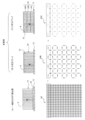
- the PET detector 10 includes a scintillator array 14 optically connected on a light receiving surface of the light receiving element array 12.
- 8 is radiation
- 12A is a light receiving element
- 16 is a reflector
- 18 is a light guide for diffusing light
- 20 is a resistance chain
- 22 is an analog-to-digital converter (ADC)
- 24 is a two-dimensional position histogram. ..
- the center of gravity calculation (FIG. 1 (D)) described in Patent Document 1 is used in order to simplify the signal processing, but an error occurs in the process of the calculation. Further, since the distribution of light is limited in the peripheral portion of the scintillator array 14, the scintillator identification performance deteriorates when a minute scintillator is used.
- a digital PET detector 10A in which the unit scintillator 14A and the unit light receiving element 12A and the ADC 22A have a one-to-one correspondence as illustrated in FIG. 2 is also used.
- the size of the scintillator array 14 is limited to the same size as the light receiving element array 12, and it is necessary to prepare a signal processing circuit (ADC22A) for each unit light receiving element 12A.
- Non-Patent Document 1 proposes a method of optically connecting a light receiving element to the upper and lower surfaces of a digital PET detector and detecting the depth from the output ratio.
- Non-Patent Document 2 in order to reduce the number of light receiving elements, a pair of scintillators are arranged so as to straddle the pair of light receiving elements to provide an optical path.
- a three-dimensional digital PET detector that discriminates the depth with a light receiving element only on the bottom surface by controlling has also been proposed.
- Non-Patent Document 3 describes that four scintillators are assigned to one light receiving element.
- Japanese Unexamined Patent Publication No. 2013-246156 Japanese Unexamined Patent Publication No. 2016-17851 Japanese Unexamined Patent Publication No. 2013-140024 JP-A-2009-53104 Japanese Unexamined Patent Publication No. 2016-145819 Japanese Unexamined Patent Publication No. 2017-72573
- the general PET detector illustrated in FIG. 1 is composed of a minute scintillator (14) and a small number of light receiving elements 12A, and is capable of efficient detection, but causes an error in the process of analog calculation.
- a digital PET detector that does not cause a calculation error by associating the unit scintillator 14A and the light receiving element 12A in a ratio of 1: 1 as illustrated in FIG. 2 has also been developed, but the size of the scintillator depends on the size of the light receiving element. Not only is this limited, but an arithmetic circuit (for example, ADC 22A) is required for each light receiving element 12A.
- Non-Patent Document 2 has 4 or 16 4 ⁇ 4 unit scintillators, and is adapted to correspond to a 2 ⁇ 2 or 8 ⁇ 8 light receiving element array.
- the specific configuration is different from that of the present invention, including the fact that the array has only one stage.
- the present invention has been made to solve the above-mentioned conventional problems, and even if the size of the scintillator is smaller than the size of the light receiving element, not only can it be identified without causing a calculation error, but also depth information can be acquired.
- An object of the present invention is to provide a radiation position detector.
- the present invention is a unit size in a radiation position detector in which a scintillator is optically connected on the light receiving surface of the light receiving element, the response of the scintillator element that detects radiation is identified on the light receiving surface, and the radiation detection position is obtained.
- a scintillator array consisting of a light receiving element array in which the unit light receiving elements of No. 1 are arranged in a two-dimensional plane and a plurality of scintillator elements optically connected to the light receiving element array, and the cross-sectional size of the incident surface is the size of the unit light receiving element.
- a set of two unit scintillators which has an area of 1/4 of that of the scintillator, is arranged so that at least a part of the incident surface side is optically connected and the other part is separated by a reflective material across the two unit light receiving elements.
- the scintillator unit is specified by the presence or absence of the light receiving signal in each unit light receiving element, and further, one unit scintillator of the scintillator unit is specified based on the strength of the light receiving signal when there is a signal.
- the scintillator unit can be arranged so as to straddle the unit light receiving element and the light receiving elements on four sides adjacent thereto.
- the detection depth can be identified from the output ratio of the light receiving element corresponding to the scintillator unit.
- the unit scintillator can be specified in two dimensions by calculating the center of gravity.
- the unit scintillator can be pixelated in the detection depth direction as well.
- the number of scintillator units constituting the two-dimensional scintillator array on the radiation incident side by providing a plurality of stages of the two-dimensional scintillator array in the detection depth direction is the number of scintillator units constituting the two-dimensional scintillator array on the light receiving element array side. Can be smaller than.
- the size of the scintillator that is, the spatial resolution (for example, 4 mm) can be reduced to 1/2 (for example, 2 mm) of the size of the unit light receiving element without incurring a large cost. Therefore, if the size of the unit light receiving element is the same, the number of unit scintillators can be increased to improve the spatial resolution of the digital detector. Alternatively, if the number of unit scintillators is the same (small size), the size of the unit light receiving element should be halved, the digital detector should be miniaturized, and it should be used for helmet-type PET for the brain and PET for small animals. Can be done.
- the figure which shows the structural example of the conventional general PET detector Similarly, a diagram showing a configuration example of a digital PET detector.
- the figure which shows the embodiment of this invention Top view showing the configuration in the case of 3 ⁇ 3 Similarly, a diagram showing an example of a scintillator arrangement pattern with respect to a central light receiving element and a scintillator identification method at the center in the case of 3 ⁇ 3.
- Top view showing how to identify the end showing another example of the arrangement pattern of the scintillator with respect to the central light receiving element.
- Example 2 of three layers when the center of gravity calculation is added
- enlarged view Top view showing a comparison between (A) a conventional optical distribution method and (B) a two-dimensional position histogram of Example 3 according to the method of the present invention in the calculation of the center of gravity of four layers.
- a scintillator is optically connected on the light receiving surface of the light receiving element, and the response of the scintillator element that detects radiation is transmitted on the light receiving surface.
- a digital PET detector which is a radiation position detector that identifies and obtains a radiation detection position
- a unit-sized approximate rectangular light-receiving element (simply referred to as a light-receiving element) 12A is densely arranged on a two-dimensional plane.
- a scintillator array 30 composed of an element array 12 and a plurality of scintillator elements (also referred to as unit scintillators) 36 optically connected to the light receiving element array 12, and the cross-sectional size of the incident surface is 1 / of the size of the light receiving element 12A.
- the scintillator unit 38 is specified by the scintillator array 30 in which the isolated scintillator units 38 are arranged so as to straddle the two light receiving elements 12A and the presence or absence of the light receiving signal in each light receiving element 12A, and further, the received light signal when there is a signal
- a position evaluation unit 40 for obtaining a two-dimensional radiation detection position by specifying one unit scintillator 36 of the scintillator unit 38 based on the strength of the scintillator unit 38 is provided.
- the scintillator can be composed of, for example, GAGG, LFS, LYSO, or the like, and the light receiving element array 12 can be composed of, for example, a semiconductor light receiving element such as MPPC or SiPM.
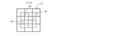
- FIG. 4 shows an arrangement example of the scintillator array 30 and the light receiving element array 12 when the number of light receiving elements is 3 ⁇ 3.
- the scintillator units 38A to 38D are arranged so as to straddle the four sides around the central light receiving element 12C. That is, the scintillator units 38A to 38D are arranged so as to evenly straddle the central light receiving element 12C and the other light receiving elements 12E, 12G, 12I, and 12K adjacent to the center light receiving element 12C.
- the scintillator unit 38A on the upper left emits light as shown in (a).
- the scintillator unit 38B on the lower left emits light as shown in (b).
- the scintillator unit 38C on the lower right side emits light as shown in (c).
- the scintillator unit 38D on the upper right emits light as shown in (d).
- the ratio of the outputs of the unit scintillators A and B in the scintillator units 38A to 38D changes as shown in the second stage of FIG. 5B depending on the incident position on the unit scintillators A and B. Therefore, the one with the larger output can be identified as the unit scintillator in which the radiation is incident. Further, the position in the depth direction can be specified by the output ratio of A and B.
- the incident position can be specified as shown in FIG.
- the scintillator unit 38E on the upper left emits light as shown in (a).
- the scintillator unit 38F on the lower left emits light as shown in (b).
- the lower right scintillator unit 38G emits light as shown in (c).
- the scintillator unit 38H on the upper right emits light as shown in (d). Therefore, as in FIG. 5B, the unit scintillator having the larger output may be specified.
- the arrangement of the scintillator with respect to the central light receiving element 12C is not limited to FIG. 5, and may be as shown in FIG.
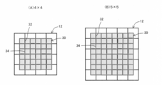
- the number of light receiving elements in the light receiving element array 12 is not 3 ⁇ 3 shown in FIGS. 4 to 7, but 4 ⁇ 4 shown in FIG. 8 (A), 5 ⁇ 5 shown in FIG. 8 (B), and the like. You may.
- the signal processing used in the present invention includes an independent signal readout (also referred to as digital readout) in which the ADC 22 is directly connected to each light receiving element 12A as shown in FIG. 9A, and a resistor as shown in FIG. 9B. It may be an analog readout in which the two-dimensional position histogram 24 is obtained by the calculation of the center of gravity via the chain 20.
- FIG. 10 (A) a two-dimensional position histogram 24 in a general PET detector, (B) a two-dimensional position histogram 24B in the case of a two-dimensional array according to the present invention, and (C) a three-stage scintillator array 30A to An example of a two-dimensional position histogram 24C in the case of a three-dimensional array provided with 30C is shown in comparison.
- the scintillator is projected onto the line reflecting the detection depth, and the number of points increases according to the number of stages of the array in the depth direction. You can see that.
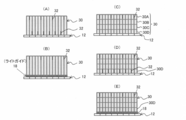
- the scintillator array 30 has one or three stages, and the optical adhesive 32 is arranged on the radiation incident side (upper side of the figure), but the modified example shown in FIG. 11 is shown. As shown in (A), the optical adhesive 32 is also provided on the light receiving element array 12 side of the one-stage scintillator array 30 to improve the light detection efficiency, or as shown in (B), the one-stage scintillator array.
- the light guide 18 is inserted between the 30 and the light receiving element array 12, or as shown in (C), the number of stacking stages of the scintillator array 30 is multiple (4 stages of 30A to 30D in the figure), or (D).
- the scintillator array 30 has a plurality of stages (4 stages of 30A to 30D in the figure), and the optical adhesive 32 is also arranged on the scintillator array 30D on the light receiving element array 12 side to improve the light detection efficiency.
- the light guide 18 can be inserted between the light receiving element array 12 and the scintillator array 30 in the scintillator array 30 having a plurality of stages (4 stages of 30A to 30D in the figure).
- the arrangement position of the optical adhesive 32, the presence / absence of the light guide 18, and the number of stages of the scintillator array 30 can be appropriately set.
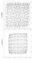
- the scintillator array is a rectangular parallelepiped as shown in FIG. 12 (A), but in this case, as shown in FIG. 12 (B), the overlapping regions are formed when arranged in a ring shape. appear.
- the number of scintillators is reduced toward the radiation incident side by using a plurality of scintillator arrays (three stages of 30A to 30C in the figure), and a stepped pyramid type is used.
- FIG. 12 (D) shows a configuration example of the scintillator array in each stage 30A to 30C.
- FIG. 13 shows Example 1 of a signal in digital processing when an LFS unit scintillator 36 of 3.1 ⁇ 3.1 ⁇ 20 mm is used.
- 36A is an optical discontinuity provided in the unit scintillator 36 by, for example, a laser.
- the unit scintillator 1 side in the example of the 1-2 scintillator unit With the center in between, the unit scintillator 1 side in the example of the 1-2 scintillator unit, the 2 side in the 2-5 example, the 3 side in the 3-6 example, and the 5 side in the 4-5 example. It can be identified that the radiation is incident on the 5 side in the example of 5-6, on the 8 side in the example of 5-8, on the 4 side in the example of 4-7, and on the 9 side in the example of 8-9. ..
- FIG. 14 shows Example 2 of a two-dimensional position histogram when the center of gravity is calculated in three layers using a 1.45 ⁇ 1.45 ⁇ 4.5 mm GAGG unit scintillator and a 3 ⁇ 3 mm MPPC light receiving element array. Shown in. As shown enlarged in FIG. 15, it is clear that the points on the line are separated.
- FIG. 16 shows (A) the optical distribution method described in Patent Document 4 when the center of gravity is calculated by the same 4-layer GAGG scintillator array, and (B) the two-dimensional position histogram of Example 3 in the case of the method of the present invention. Shown by comparison. Compared with the optical distribution method described in Patent Document 4, the two-dimensional position histogram is wider, and it is clear that the discriminating ability is improved.
- a head PET device such as a helmet type or a PET device for small animals proposed by the applicant requires a higher resolution than a whole body screening test for cancer, but according to the present invention, an existing resolution of, for example, 4 mm is required. Can be improved to half 2 mm without incurring a large cost, and depth detection is also possible.
- the present invention has been applied to a three-dimensional digital PET detector, but the application target of the present invention is not limited to this, and it is clear that the present invention can be similarly applied to a radiation detector other than PET. Is.
- the present invention is useful for a head PET device such as a PET device, particularly a helmet-type PET device, which requires higher resolution than a whole-body screening test for cancer.
Landscapes
- Physics & Mathematics (AREA)
- Health & Medical Sciences (AREA)
- Life Sciences & Earth Sciences (AREA)
- General Physics & Mathematics (AREA)
- High Energy & Nuclear Physics (AREA)
- Molecular Biology (AREA)
- Spectroscopy & Molecular Physics (AREA)
- Engineering & Computer Science (AREA)
- Biomedical Technology (AREA)
- General Health & Medical Sciences (AREA)
- Medical Informatics (AREA)
- Nuclear Medicine, Radiotherapy & Molecular Imaging (AREA)
- Optics & Photonics (AREA)
- Nuclear Medicine (AREA)
- Measurement Of Radiation (AREA)
Abstract
単位サイズの単位受光素子(12A、12C~12K)を2次元平面状に配置した受光素子アレイ12と、該受光素子アレイ12に光学接続される複数シンチレータ素子(36)からなるシンチレータアレイ30であって、入射面の断面サイズが、単位受光素子のサイズの1/4の面積である単位シンチレータ36を2個1組として、少なくとも入射面側の一部を光学接続し、それ以外を反射材34で隔離したシンチレータユニット38、38A~38Hを、2つの単位受光素子に跨いで配置したシンチレータアレイと、各単位受光素子における受光信号の有無により、シンチレータユニットを特定し、更に、信号が有る場合の前記受光信号の強弱に基づき、前記シンチレータユニットの一方の単位シンチレータを特定することにより2次元放射線検出位置を得る位置評価部40とを有する。これにより、デジタル検出器の空間分解能を、大きなコストを掛けずに2倍に向上する。
Description
本発明は、放射線位置検出器に係り、特に、ポジトロンイメージング装置や陽電子放射断層像撮像(PET)装置等の核医学イメージングの分野で用いるのに好適な放射線位置検出器に関する。
PETでは、511keVのガンマ線を検出するために、シンチレータと受光素子を光学接続した放射線位置検出器が用いられる。したがって、シンチレータの入射面に対する断面サイズが画質を大きく左右する。また、シンチレータの厚さは約3cmであり、この厚さが斜め入射のガンマ線を検出する際、画質を劣化させる。この問題を解決するために、シンチレータとガンマ線が相互作用した深さ位置を検出可能な3次元PET検出器も多数開発されている。
一般的なPET検出器を図1に例示する。このPET検出器10は、受光素子アレイ12の受光面上に光学接続されたシンチレータアレイ14を備えている。図において8は放射線、12Aは受光素子、16は反射材、18は光を拡散するためのライトガイド、20は抵抗チェーン、22はアナログデジタル変換器(ADC)、24は2次元位置ヒストグラムである。
このようなPET検出器では、信号処理を簡略化するため、例えば特許文献1に記載されているような重心演算(図1(D))が用いられるが、演算の過程で誤差を生じる。また、シンチレータアレイ14の周辺部では光の分布が制限されるため、微小なシンチレータを用いる場合シンチレータ識別の性能が劣化する。
一方、図2に例示するような、単位シンチレータ14Aと単位受光素子12A及びADC22Aを1対1対応させたデジタルPET検出器10Aも利用されている。しかしながら、シンチレータアレイ14のサイズは受光素子アレイ12と同じサイズに制限され、信号処理回路(ADC22A)も単位受光素子12Aごとに用意する必要がある。
一方、深さ方向の位置も検出可能な3次元PET検出器としては、特許文献2に記載されているように、特性の異なる2種類のシンチレータアレイを積層したり、特許文献3に記載されているように、上下面に受光素子を光学接続して出力比を利用したり、特許文献4に記載されているように、光学反射材やシンチレータの配置を層ごとに最適化して重心演算上で識別する方法が提案されている。又、非特許文献1には、デジタルPET検出器の上下面に受光素子を光学接続し、出力比から深さ検出する方法が提案されている。更に、特許文献5、6や非特許文献2に記載されているように、受光素子の数を低減するために1対のシンチレータを1対の受光素子に跨るように配置して光の経路を制御することで、底面のみの受光素子で深さ識別を行う3次元デジタルPET検出器も提案されている。又、非特許文献3には4つのシンチレータを1つの受光素子に割り当てることが記載されている。
W.W.Moses, et al., "Performance of a PET detector module utilizing an array of silicon photodiodes to identify the crystal of interaction", IEEE Trans. Nucl. Sci. Vol 40, 1036-1040, 1993.
H.Uchida, T.Sakai, H.Yamauchi, K.Hakamata, K.Shimizu,"A novel single-ended readout depth-of-interaction PET detector fabricated using sub-surface laser engraving", Phy. Med. Bio., 61(2016)6635
Zhang. et. al "A depth encoding PET detector using four-crystals-to-one-SiPM coupling and light-sharing window method" Medical Physics, https://aapm.onlinelibrary.wiley.com/doi/full/10.1002/mp.13603, 20 May 2019
図1に例示した一般的なPET検出器は、微小なシンチレータ(14)と少数の受光素子12Aから構成され、効率的な検出が可能であるが、アナログ演算の過程で誤差を生じる。一方、図2に例示したような、単位シンチレータ14Aと受光素子12Aを1:1で対応させることで演算誤差を生じないデジタルPET検出器も開発されているが、受光素子のサイズによってシンチレータのサイズが制限されるだけでなく、受光素子12Aごとに演算回路(例えばADC22A)を必要とする。
又、非特許文献2に記載の放射線位置検出器は、4×4の単位シンチレータが4個又は16個で、2×2又は8×8の受光素子アレイに対応するようにされており、シンチレータアレイが1段しかない点も含め、本発明とは具体的な構成が異なっている。
本発明は、前記従来の問題点を解消するべくなされたもので、シンチレータのサイズを受光素子のサイズよりも小さくしても、演算誤差を生じずに識別できるだけでなく、深さ情報も取得可能な放射線位置検出器を提供することを課題とする。
本発明は、受光素子の受光面上にシンチレータを光学接続し、放射線を検出したシンチレータ素子の応答を受光面上で識別して、放射線検出位置を得るようにした放射線位置検出器において、単位サイズの単位受光素子を2次元平面状に配置した受光素子アレイと、該受光素子アレイに光学接続される複数シンチレータ素子からなるシンチレータアレイであって、入射面の断面サイズが、前記単位受光素子のサイズの1/4の面積である単位シンチレータを2個1組として、少なくとも入射面側の一部を光学接続し、それ以外を反射材で隔離したシンチレータユニットを、2つの単位受光素子に跨いで配置したシンチレータアレイと、各単位受光素子における受光信号の有無により、シンチレータユニットを特定し、更に、信号が有る場合の前記受光信号の強弱に基づき、前記シンチレータユニットの一方の単位シンチレータを特定することにより2次元放射線検出位置を得る位置評価部と、を有することにより、前記課題を解決するものである。
ここで、前記シンチレータユニットを、前記単位受光素子とそれに隣接する四方の受光素子とを跨ぐように配置することができる。
又、前記シンチレータユニットに対応する受光素子の出力比から検出深さを識別するようにすることができる。
又、前記単位シンチレータの特定を、重心演算により2次元上で行うようにすることができる。
又、前記単位シンチレータを検出深さ方向にもピクセル化することができる。
又、2次元シンチレータアレイを検出深さ方向に複数段設け、放射線入射側の2次元シンチレータアレイを構成するシンチレータユニットの数を、前記受光素子アレイ側の2次元シンチレータアレイを構成するシンチレータユニットの数よりも小とすることができる。
本発明によれば、シンチレータのサイズ即ち空間分解能(例えば4mm)を、大きなコストを掛けずに単位受光素子のサイズの1/2(例えば2mm)に小さくすることができる。従って、単位受光素子のサイズが同じであれば、単位シンチレータの数を増やしてデジタル検出器の空間分解能を向上することができる。或いは、単位シンチレータの数が同じ(サイズは小)であれば、単位受光素子のサイズを半分にし、デジタル検出器を小型化して、脳に用いるヘルメット型のPETや小動物用のPETにも用いることができる。
更に、この検出器に重心演算を適用した場合、個々のシンチレータの分布は検出深さ情報を含んだ形で線状に局所的に投影されるため、低コストで演算誤差を大幅に低減できる。
以下、図面を参照して、本発明の実施の形態について詳細に説明する。なお、本発明は以下の実施形態及び実施例に記載した内容により限定されるものではない。又、以下に記載した実施形態及び実施例における構成要件には、当業者が容易に想定できるもの、実質的に同一のもの、いわゆる均等の範囲のものが含まれる。更に、以下に記載した実施形態及び実施例で開示した構成要素は適宜組み合わせてもよいし、適宜選択して用いてもよい。
本発明の実施形態は、図3(A)上面図及び(B)側面図に示す如く、受光素子の受光面上にシンチレータを光学接続し、放射線を検出したシンチレータ素子の応答を受光面上で識別して、放射線検出位置を得るようにした放射線位置検出器であるデジタルPET検出器において、単位サイズの略方形受光素子(単に受光素子と称する)12Aを2次元平面上に稠密に配置した受光素子アレイ12と、該受光素子アレイ12に光学接続される複数シンチレータ素子(単位シンチレータとも称する)36からなるシンチレータアレイ30であって、入射面の断面サイズが、前記受光素子12Aのサイズの1/4(ピッチは1/2)である単位シンチレータ36を2個1組として、入射面側の一部を光学接着剤32で光学接続し、それ以外を反射材(例えばポリテトラフルオロエチレン)34で隔離したシンチレータユニット38を、2つの受光素子12Aに跨いで配置したシンチレータアレイ30と、各受光素子12Aにおける受光信号の有無により、シンチレータユニット38を特定し、更に、信号が有る場合の前記受光信号の強弱に基づき、前記シンチレータユニット38の一方の単位シンチレータ36を特定することにより2次元放射線検出位置を得る位置評価部40と、を備えたものである。
前記シンチレータは、例えばGAGG、LFS、LYSO等で構成することができ、前記受光素子アレイ12は、例えばMPPC、SiPM等の半導体受光素子で構成することができる。
受光素子12Aのサイズの1/4のシンチレータを識別可能であるので、例えば4mm角のSiPMを用いる場合は2mm角の単位シンチレータを用いる。又、SiPMアレイが8×8である場合、シンチレータアレイは14×14が最大となる。
受光素子数が3×3である場合のシンチレータアレイ30と受光素子アレイ12の配置例を図4に示す。
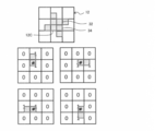
ここで、図5に示す如く、中央の受光素子12Cに着目すると、4組のシンチレータユニット38A~38Dが中央の受光素子12Cの周囲の4辺を跨るように配置されている。すなわち中央の受光素子12Cと、その四方に隣接する他の受光素子12E、12G、12I、12Kとを均等に跨いでシンチレータユニット38A~38Dが配置されている。
このうち、図5(A)第1段階として、中央の受光素子12Cの左上部に放射線が入射した場合には、(a)に示すように、左上のシンチレータユニット38Aが発光する。又、中央の受光素子12Cの左下部に放射線が入射した場合には、(b)に示すように、左下のシンチレータユニット38Bが発光する。又、中央の受光素子12Cの右下部に放射線が入射した場合には、(c)に示すように、右下のシンチレータユニット38Cが発光する。又、中央の受光素子12Cの右上部に放射線が入射した場合には、(d)に示すように、右上のシンチレータユニット38Dが発光する。
各シンチレータユニット38A~38Dにおける各単位シンチレータA、Bの出力の比は、単位シンチレータA、Bへの入射位置に応じて図5(B)第2段階のように変化する。従って、出力が大きい方を放射線が入射した単位シンチレータと特定できる。更に、AとBの出力比により、深さ方向位置も特定できる。
図5にシンチレータユニットが図示されていなかった端の受光素子12D~12Kに放射線が入射した場合にも、図6に示す如く入射位置を特定できる。
即ち、左又は上の受光素子12D又は12K(図では12D)に放射線が入射した場合は、(a)に示すように、左上のシンチレータユニット38Eが発光する。又、左又は左下の受光素子12E又は12F(図では12E)に放射線が入射した場合には、(b)に示すように、左下のシンチレータユニット38Fが発光する。又、下又は右下の受光素子12G又は12H(図では12H)に放射線が入射した場合は、(c)に示すように、右下のシンチレータユニット38Gが発光する。又、右又は右上の受光素子12I又は12J(図では12I)に放射線が入射した場合は、(d)に示すように、右上のシンチレータユニット38Hが発光する。従って、図5(B)と同様に出力の大きい方の単位シンチレータを特定すれば良い。
なお、中央の受光素子12Cに対するシンチレータの配置は、図5に限定されず、図7のようであっても良い。
又、受光素子アレイ12の受光素子数も図4~図7に示した3×3でなく、図8(A)に示す4×4や、図8(B)に示す5×5などであっても良い。
本発明で用いる信号処理は、図9(A)に示すように各受光素子12AにADC22が直接接続された独立信号読み出し(デジタル読み出しとも称する)の他、図9(B)に示す如く、抵抗チェーン20を介した重心演算で2次元位置ヒストグラム24を得るようにしたアナログ読み出しであっても良い。
図10に、(A)一般的なPET検出器における2次元位置ヒストグラム24と、本発明による(B)2次元アレイの場合の2次元位置ヒストグラム24B及び同じく(C)3段のシンチレータアレイ30A~30Cを備えた3次元アレイである場合の2次元位置ヒストグラム24Cの例を比較して示す。図10(A)の一般的なPET検出器の場合、検出した光子数によるばらつきを生じる。これに対して図10(B)、(C)の本発明による場合は、シンチレータが検出深さを反映してライン上に投影され、深さ方向のアレイの段数に応じて点の数が増えていることが分かる。
又、これまでの実施形態においては、シンチレータアレイ30が1段又は3段とされ、その放射線入射側(図の上側)に光学接着剤32が配置されていたが、図11に示す変形例のように、(A)に示す如く、1段シンチレータアレイ30の受光素子アレイ12側にも光学接着剤32を設けて光の検出効率を向上したり、(B)に示す如く、1段シンチレータアレイ30と受光素子アレイ12の間にライトガイド18を挿入したり、或いは、(C)に示す如く、シンチレータアレイ30の積層段数を複数(図では30A~30Dの4段)としたり、或いは(D)に示す如く、複数段(図では30A~30Dの4段)のシンチレータアレイ30で受光素子アレイ12側のシンチレータアレイ30Dにも光学接着剤32を配置して光の検出効率を向上したり、或いは(E)に示す如く、複数段(図では30A~30Dの4段)のシンチレータアレイ30で受光素子アレイ12とシンチレータアレイ30の間にライトガイド18を挿入したりすることが可能であり、光学接着剤32の配設位置、ライトガイド18の有無、シンチレータアレイ30の段数は、適宜設定可能である。
又、前記実施形態では、いずれもシンチレータアレイが図12(A)に示すように直方体とされていたが、この場合は、図12(B)に示す如く、リング状に配置した場合重なる領域が発生する。これに対して図12(C)に示す実施形態のように、シンチレータアレイを複数段(図では30A~30Cの3段)として、放射線入射側に向けてシンチレータの数を減らし階段状のピラミッド型とした場合には、図12(D)に示すように、リング状に配置する場合にも隙間なく配置して立体角を向上することができる。各段30A~30Cにおけるシンチレータアレイの構成例を図12(E)に示す。
3.1×3.1×20mmのLFS単位シンチレータ36を用いた場合のデジタル処理における信号の実施例1を図13に示す。図において、36Aは、例えばレーザによって単位シンチレータ36内に設けられた光学的不連続面である。
中心をはさんで、1-2のシンチレータユニットの例では単位シンチレータ1側に、2-5の例では2側に、3-6の例では3側に、4-5の例では5側に、5-6の例では5側に、5-8の例では8側に、4-7の例では4側に、8-9の例では9側に放射線が入射していることが識別できる。
又、1.45×1.45×4.5mmのGAGG単位シンチレータと3×3mmのMPPC受光素子アレイを用いて3層で重心演算を行った場合の2次元位置ヒストグラムの実施例2を図14に示す。図15に拡大して示す如く、ライン上の点が分離できていることが明らかである。
同じく4層のGAGGシンチレータアレイで重心演算を行った場合における(A)特許文献4に記載の光分配方式と、(B)本発明法による場合の実施例3の2次元位置ヒストグラムを図16に比較して示す。特許文献4に記載の光分配方式に比べて2次元位置ヒストグラムが広がっており、識別能が改善していることが明らかである。
出願人が提案したヘルメット型のような頭部PET装置や小動物用PET装置においては、癌の全身スクリーニング検査と比べて高い分解能を必要とするが、本発明によれば、既存の例えば4mmの分解能を、大きなコストをかけずに半分の2mmに向上することができ、更に深さ検出も可能となる。
なお、前記実施形態においては、本発明が3次元デジタルPET検出器に適用されていたが、本発明の適用対象はこれに限定されず、PET以外の放射線検出器にも同様に適用できることは明らかである。
本発明は、PET装置、特にヘルメット型PET装置など、癌の全身スクリーニング検査と比べても高い分解能を必要とする頭部PET装置に有用である。
10…PET検出器
12…受光素子アレイ
12A、12C~12K…受光素子
14、30、30A~30D…シンチレータアレイ
16、34…反射材
18…ライトガイド
20…抵抗チェーン
22、22A…アナログ-デジタル変換器(ADC)
24、24B、24C…2次元位置ヒストグラム
32…光学接着剤
36…単位シンチレータ
38、38A~38H…シンチレータユニット
40…位置評価部
12…受光素子アレイ
12A、12C~12K…受光素子
14、30、30A~30D…シンチレータアレイ
16、34…反射材
18…ライトガイド
20…抵抗チェーン
22、22A…アナログ-デジタル変換器(ADC)
24、24B、24C…2次元位置ヒストグラム
32…光学接着剤
36…単位シンチレータ
38、38A~38H…シンチレータユニット
40…位置評価部
Claims (6)
- 受光素子の受光面上にシンチレータを光学接続し、放射線を検出したシンチレータ素子の応答を受光面上で識別して、放射線検出位置を得るようにした放射線位置検出器において、
単位サイズの単位受光素子を2次元平面状に配置した受光素子アレイと、
該受光素子アレイに光学接続される複数シンチレータ素子からなるシンチレータアレイであって、入射面の断面サイズが、前記単位受光素子のサイズの1/4の面積である単位シンチレータを2個1組として、少なくとも入射面側の一部を光学接続し、それ以外を反射材で隔離したシンチレータユニットを、2つの単位受光素子に跨いで配置したシンチレータアレイと、
各単位受光素子における受光信号の有無により、シンチレータユニットを特定し、更に、信号が有る場合の前記受光信号の強弱に基づき、前記シンチレータユニットの一方の単位シンチレータを特定することにより2次元放射線検出位置を得る位置評価部と、
を有することを特徴とする放射線位置検出器。 - 前記シンチレータユニットが、前記単位受光素子とそれに隣接する四方の受光素子とを跨ぐように配置されていることを特徴とする請求項1に記載の放射線位置検出器。
- 前記シンチレータユニットに対応する受光素子の出力比から検出深さを識別するようにされていることを特徴とする請求項1又は2に記載の放射線位置検出器。
- 前記単位シンチレータの特定を、重心演算により2次元上で行うようにされていることを特徴とする請求項1乃至3のいずれかに記載の放射線位置検出器。
- 前記単位シンチレータが検出深さ方向にもピクセル化されていることを特徴とする請求項1に記載の放射線位置検出器。
- 2次元シンチレータアレイが検出深さ方向に複数段設けられ、放射線入射側の2次元シンチレータアレイを構成するシンチレータユニットの数が、前記受光素子アレイ側の2次元シンチレータアレイを構成するシンチレータユニットの数よりも小とされていることを特徴とする請求項5に記載の放射線位置検出器。
Priority Applications (3)
| Application Number | Priority Date | Filing Date | Title |
|---|---|---|---|
| JP2021530596A JP7384454B2 (ja) | 2019-07-08 | 2020-06-26 | 放射線位置検出器 |
| EP20836254.1A EP3998499A4 (en) | 2019-07-08 | 2020-06-26 | RADIATION POSITION DETECTOR |
| US17/619,962 US11982777B2 (en) | 2019-07-08 | 2020-06-26 | Radiation position detector |
Applications Claiming Priority (2)
| Application Number | Priority Date | Filing Date | Title |
|---|---|---|---|
| JP2019-126957 | 2019-07-08 | ||
| JP2019126957 | 2019-07-08 |
Publications (1)
| Publication Number | Publication Date |
|---|---|
| WO2021006061A1 true WO2021006061A1 (ja) | 2021-01-14 |
Family
ID=74114712
Family Applications (1)
| Application Number | Title | Priority Date | Filing Date |
|---|---|---|---|
| PCT/JP2020/025134 Ceased WO2021006061A1 (ja) | 2019-07-08 | 2020-06-26 | 放射線位置検出器 |
Country Status (4)
| Country | Link |
|---|---|
| US (1) | US11982777B2 (ja) |
| EP (1) | EP3998499A4 (ja) |
| JP (1) | JP7384454B2 (ja) |
| WO (1) | WO2021006061A1 (ja) |
Cited By (1)
| Publication number | Priority date | Publication date | Assignee | Title |
|---|---|---|---|---|
| WO2024111385A1 (ja) * | 2022-11-24 | 2024-05-30 | 国立研究開発法人量子科学技術研究開発機構 | シンチレータアレイ、放射線検出装置、及び陽電子放出断層撮影装置 |
Citations (11)
| Publication number | Priority date | Publication date | Assignee | Title |
|---|---|---|---|---|
| JPH0651069A (ja) * | 1992-07-28 | 1994-02-25 | Hamamatsu Photonics Kk | 放射線検出器 |
| JP2003240857A (ja) * | 2002-02-19 | 2003-08-27 | Shimadzu Corp | 放射線検出器 |
| JP2009053104A (ja) | 2007-08-28 | 2009-03-12 | Natl Inst Of Radiological Sciences | 放射線位置検出器 |
| US20110192982A1 (en) * | 2010-02-01 | 2011-08-11 | Siemens Medical Solutions Usa, Inc. | System and Method for Providing Depth of Interaction Detection Using Positron Emission Tomography |
| JP2013140024A (ja) | 2011-12-28 | 2013-07-18 | Waseda Univ | 放射線検出器 |
| JP2013246156A (ja) | 2012-05-29 | 2013-12-09 | Natl Inst Of Radiological Sciences | 3次元放射線位置検出器 |
| US20150226862A1 (en) * | 2009-10-27 | 2015-08-13 | University Of Washington Through Its Center For Commercialization | Optical-interface patterning for radiation detector crystals |
| JP2016017851A (ja) | 2014-07-08 | 2016-02-01 | 株式会社島津製作所 | 放射線撮影装置 |
| JP2016145819A (ja) | 2015-01-30 | 2016-08-12 | 浜松ホトニクス株式会社 | 放射線検出器 |
| WO2017046928A1 (ja) * | 2015-09-17 | 2017-03-23 | 株式会社島津製作所 | 情報処理装置、放射線検出器、放射線撮影装置、およびプログラム |
| JP2017072573A (ja) | 2015-01-30 | 2017-04-13 | 浜松ホトニクス株式会社 | 放射線検出器 |
Family Cites Families (5)
| Publication number | Priority date | Publication date | Assignee | Title |
|---|---|---|---|---|
| US8933410B2 (en) * | 2010-03-29 | 2015-01-13 | National Institute Of Radiological Sciences | Three-dimensional position-sensitive radiation detector and method of identifying radiation detected positions therein |
| WO2016059557A1 (en) * | 2014-10-17 | 2016-04-21 | Koninklijke Philips N.V. | Pet detector scintillator arrangement with light sharing and depth of interaction estimation |
| US9753149B2 (en) | 2015-01-30 | 2017-09-05 | Hamamatsu Photonics K.K. | Radiation detector |
| US10094937B2 (en) | 2015-01-30 | 2018-10-09 | Hamamatsu Photonics K.K. | Radiation detector |
| CN107710019B (zh) * | 2015-06-24 | 2019-09-13 | 株式会社岛津制作所 | 放射线检测器以及具备该放射线检测器的放射线摄影装置 |
-
2020
- 2020-06-26 EP EP20836254.1A patent/EP3998499A4/en active Pending
- 2020-06-26 WO PCT/JP2020/025134 patent/WO2021006061A1/ja not_active Ceased
- 2020-06-26 US US17/619,962 patent/US11982777B2/en active Active
- 2020-06-26 JP JP2021530596A patent/JP7384454B2/ja active Active
Patent Citations (11)
| Publication number | Priority date | Publication date | Assignee | Title |
|---|---|---|---|---|
| JPH0651069A (ja) * | 1992-07-28 | 1994-02-25 | Hamamatsu Photonics Kk | 放射線検出器 |
| JP2003240857A (ja) * | 2002-02-19 | 2003-08-27 | Shimadzu Corp | 放射線検出器 |
| JP2009053104A (ja) | 2007-08-28 | 2009-03-12 | Natl Inst Of Radiological Sciences | 放射線位置検出器 |
| US20150226862A1 (en) * | 2009-10-27 | 2015-08-13 | University Of Washington Through Its Center For Commercialization | Optical-interface patterning for radiation detector crystals |
| US20110192982A1 (en) * | 2010-02-01 | 2011-08-11 | Siemens Medical Solutions Usa, Inc. | System and Method for Providing Depth of Interaction Detection Using Positron Emission Tomography |
| JP2013140024A (ja) | 2011-12-28 | 2013-07-18 | Waseda Univ | 放射線検出器 |
| JP2013246156A (ja) | 2012-05-29 | 2013-12-09 | Natl Inst Of Radiological Sciences | 3次元放射線位置検出器 |
| JP2016017851A (ja) | 2014-07-08 | 2016-02-01 | 株式会社島津製作所 | 放射線撮影装置 |
| JP2016145819A (ja) | 2015-01-30 | 2016-08-12 | 浜松ホトニクス株式会社 | 放射線検出器 |
| JP2017072573A (ja) | 2015-01-30 | 2017-04-13 | 浜松ホトニクス株式会社 | 放射線検出器 |
| WO2017046928A1 (ja) * | 2015-09-17 | 2017-03-23 | 株式会社島津製作所 | 情報処理装置、放射線検出器、放射線撮影装置、およびプログラム |
Non-Patent Citations (4)
| Title |
|---|
| H. UCHIDAT. SAKAIH. YAMAUCHIK. HAKAMATAK. SHIMIZU: "A novel single-ended readout depth-of-interaction PET detector fabricated using sub-surface laser engraving", PHY. MED. BIO., vol. 61, 2016, pages 6635, XP020308538, DOI: 10.1088/0031-9155/61/18/6635 |
| See also references of EP3998499A4 |
| W. W. MOSES ET AL.: "Performance of a PET detector module utilizing an array of silicon photodiodes to identify the crystal of interaction", IEEE TRANS. NUCL. SCI., vol. 40, 1993, pages 1036 - 1040 |
| ZHANG: "A depth encoding PET detector using four-crystals-to-one-SiPM coupling and light-sharing window method", MEDICAL PHYSICS, 20 May 2019 (2019-05-20), Retrieved from the Internet <URL:https://aapm.onlinelibrary.wiley.com/doi/full/10.1002/mp.13603> |
Cited By (1)
| Publication number | Priority date | Publication date | Assignee | Title |
|---|---|---|---|---|
| WO2024111385A1 (ja) * | 2022-11-24 | 2024-05-30 | 国立研究開発法人量子科学技術研究開発機構 | シンチレータアレイ、放射線検出装置、及び陽電子放出断層撮影装置 |
Also Published As
| Publication number | Publication date |
|---|---|
| EP3998499A1 (en) | 2022-05-18 |
| JP7384454B2 (ja) | 2023-11-21 |
| JPWO2021006061A1 (ja) | 2021-01-14 |
| US11982777B2 (en) | 2024-05-14 |
| EP3998499A4 (en) | 2023-06-14 |
| US20220357467A1 (en) | 2022-11-10 |
Similar Documents
| Publication | Publication Date | Title |
|---|---|---|
| EP2751597B1 (en) | Modelling of tof-doi detector arrays | |
| CN109765599B (zh) | 基于硅光电倍增管的探测器、机架和pet设备 | |
| JP5011590B2 (ja) | 放射線位置検出器 | |
| CN103069302B (zh) | 像素化的探测器设备 | |
| JP2004532997A (ja) | Petスキャナ | |
| JP2013246156A (ja) | 3次元放射線位置検出器 | |
| US7088901B2 (en) | Light guide apparatus and method for a detector array | |
| US11686864B2 (en) | Scintillator array with high detective quantum efficiency | |
| US20180011205A1 (en) | Combined scintillation crystal, combined scintillation detector and radiation detection device | |
| JP7384454B2 (ja) | 放射線位置検出器 | |
| JP3220239B2 (ja) | 放射線検出器 | |
| US20170329021A1 (en) | System and method for combining detector signals | |
| JP6827316B2 (ja) | 放射線位置検出方法、放射線位置検出器及びpet装置 | |
| KR101587339B1 (ko) | 양전자방출 단층촬영장치용 검출기 모듈 및 이를 이용한 양전자방출 단층촬영장치 | |
| US10539686B2 (en) | Method for the signal processing of a photosensor | |
| EP3163325B1 (en) | An apparatus and associated methods for computed tomography | |
| KR101175697B1 (ko) | Pet 모듈에서의 광자 수집 효율 및 입사한 감마선 에너지 대 광전소자 어레이에서 출력된 전자의 수 간의 선형성 향상 방법 | |
| KR20210089439A (ko) | 에너지 분리에 기반한 방사선 검출기기용 방사선(감마선) 반응 깊이 측정 방법 및 방사선(감마선) 반응 깊이 측정 장치 | |
| Dokhale et al. | Intrinsic spatial resolution and parallax correction using depth-encoding PET detector modules based on position-sensitive APD readout | |
| JPH0524068Y2 (ja) | ||
| RU197875U1 (ru) | Детектор рентгеновского излучения с составным сцинтиллятором | |
| JP5851733B2 (ja) | Pet装置及び放射線検出器ユニット | |
| KR101717954B1 (ko) | 감마/엑스선 융합 영상 검출 장치 | |
| KR101746190B1 (ko) | 섬광픽셀과 반사체 형태 조합을 이용한 양전자방출 단층촬영장치용 검출기 모듈 및 이를 이용한 양전자방출 단층촬영장치 | |
| Benlloch Baviera et al. | Device for the detection of gamma rays with interaction depth and time-of-flight encoding |
Legal Events
| Date | Code | Title | Description |
|---|---|---|---|
| 121 | Ep: the epo has been informed by wipo that ep was designated in this application |
Ref document number: 20836254 Country of ref document: EP Kind code of ref document: A1 |
|
| ENP | Entry into the national phase |
Ref document number: 2021530596 Country of ref document: JP Kind code of ref document: A |
|
| ENP | Entry into the national phase |
Ref document number: 2020836254 Country of ref document: EP Effective date: 20220208 |