WO2021010244A1 - 圧電体膜および圧電素子 - Google Patents
圧電体膜および圧電素子 Download PDFInfo
- Publication number
- WO2021010244A1 WO2021010244A1 PCT/JP2020/026652 JP2020026652W WO2021010244A1 WO 2021010244 A1 WO2021010244 A1 WO 2021010244A1 JP 2020026652 W JP2020026652 W JP 2020026652W WO 2021010244 A1 WO2021010244 A1 WO 2021010244A1
- Authority
- WO
- WIPO (PCT)
- Prior art keywords
- piezoelectric
- film
- piezoelectric film
- iron
- crystal particles
- Prior art date
- Legal status (The legal status is an assumption and is not a legal conclusion. Google has not performed a legal analysis and makes no representation as to the accuracy of the status listed.)
- Ceased
Links
Images


Classifications
-
- H—ELECTRICITY
- H10—SEMICONDUCTOR DEVICES; ELECTRIC SOLID-STATE DEVICES NOT OTHERWISE PROVIDED FOR
- H10N—ELECTRIC SOLID-STATE DEVICES NOT OTHERWISE PROVIDED FOR
- H10N30/00—Piezoelectric or electrostrictive devices
- H10N30/704—Piezoelectric or electrostrictive devices based on piezoelectric or electrostrictive films or coatings
-
- H—ELECTRICITY
- H10—SEMICONDUCTOR DEVICES; ELECTRIC SOLID-STATE DEVICES NOT OTHERWISE PROVIDED FOR
- H10N—ELECTRIC SOLID-STATE DEVICES NOT OTHERWISE PROVIDED FOR
- H10N30/00—Piezoelectric or electrostrictive devices
- H10N30/20—Piezoelectric or electrostrictive devices with electrical input and mechanical output, e.g. functioning as actuators or vibrators
- H10N30/204—Piezoelectric or electrostrictive devices with electrical input and mechanical output, e.g. functioning as actuators or vibrators using bending displacement, e.g. unimorph, bimorph or multimorph cantilever or membrane benders
- H10N30/2047—Membrane type
-
- H—ELECTRICITY
- H10—SEMICONDUCTOR DEVICES; ELECTRIC SOLID-STATE DEVICES NOT OTHERWISE PROVIDED FOR
- H10N—ELECTRIC SOLID-STATE DEVICES NOT OTHERWISE PROVIDED FOR
- H10N30/00—Piezoelectric or electrostrictive devices
- H10N30/80—Constructional details
- H10N30/85—Piezoelectric or electrostrictive active materials
- H10N30/853—Ceramic compositions
- H10N30/8542—Alkali metal based oxides, e.g. lithium, sodium or potassium niobates
-
- H—ELECTRICITY
- H10—SEMICONDUCTOR DEVICES; ELECTRIC SOLID-STATE DEVICES NOT OTHERWISE PROVIDED FOR
- H10N—ELECTRIC SOLID-STATE DEVICES NOT OTHERWISE PROVIDED FOR
- H10N30/00—Piezoelectric or electrostrictive devices
- H10N30/01—Manufacture or treatment
- H10N30/07—Forming of piezoelectric or electrostrictive parts or bodies on an electrical element or another base
- H10N30/074—Forming of piezoelectric or electrostrictive parts or bodies on an electrical element or another base by depositing piezoelectric or electrostrictive layers, e.g. aerosol or screen printing
- H10N30/077—Forming of piezoelectric or electrostrictive parts or bodies on an electrical element or another base by depositing piezoelectric or electrostrictive layers, e.g. aerosol or screen printing by liquid phase deposition
- H10N30/078—Forming of piezoelectric or electrostrictive parts or bodies on an electrical element or another base by depositing piezoelectric or electrostrictive layers, e.g. aerosol or screen printing by liquid phase deposition by sol-gel deposition
-
- H—ELECTRICITY
- H10—SEMICONDUCTOR DEVICES; ELECTRIC SOLID-STATE DEVICES NOT OTHERWISE PROVIDED FOR
- H10N—ELECTRIC SOLID-STATE DEVICES NOT OTHERWISE PROVIDED FOR
- H10N30/00—Piezoelectric or electrostrictive devices
- H10N30/01—Manufacture or treatment
- H10N30/09—Forming piezoelectric or electrostrictive materials
- H10N30/093—Forming inorganic materials
- H10N30/097—Forming inorganic materials by sintering
-
- H—ELECTRICITY
- H10—SEMICONDUCTOR DEVICES; ELECTRIC SOLID-STATE DEVICES NOT OTHERWISE PROVIDED FOR
- H10N—ELECTRIC SOLID-STATE DEVICES NOT OTHERWISE PROVIDED FOR
- H10N30/00—Piezoelectric or electrostrictive devices
- H10N30/30—Piezoelectric or electrostrictive devices with mechanical input and electrical output, e.g. functioning as generators or sensors
- H10N30/308—Membrane type
Definitions
- the present invention relates to piezoelectric membranes and piezoelectric elements.
- the present application claims priority based on Japanese Patent Application No. 2019-130521 filed in Japan on July 12, 2019, the contents of which are incorporated herein by reference.
- Piezoelectric elements having a piezoelectric film and electrodes arranged on the upper and lower surfaces of the piezoelectric film are used in various piezoelectric devices such as vibration power generation elements, sensors, actuators, inkjet heads, and autofocus.
- a KNN-based piezoelectric film made of sodium potassium niobate (KNaNbO 3 ) is known as the piezoelectric film.
- KNaNbO 3 sodium potassium niobate
- the KNN-based piezoelectric film is attracting attention as a lead-free piezoelectric film.
- a CSD method chemical solution deposition: also referred to as a chemical solution volume method or a sol-gel method
- a sputtering method is known as a method for forming a piezoelectric film.
- the CSD method is a method of forming a piezoelectric film by applying a precursor solution (or a sol-gel solution) containing a metal element having a target composition to the surface of a substrate and calcining the obtained coating film.
- the sputtering method is a method of forming a piezoelectric film by colliding, for example, ionized argon or the like with an oxide target in a high vacuum and depositing the elements ejected by the collision on a substrate.
- the CSD method is an advantageous method in that a piezoelectric film can be manufactured by using a relatively small device without requiring a high vacuum.
- the KNN-based piezoelectric film formed by a method such as the CSD method or the sputtering method may have lattice defects of the alkali metal due to scattering of the alkali metal component during the film formation.
- a piezoelectric element using a KNN-based piezoelectric film in which a lattice defect has occurred has a problem that the electromechanical conversion efficiency tends to decrease due to a leakage current generated when a voltage is applied. In order to suppress the generation of leakage current in this KNN-based piezoelectric film, it is being studied to replace a part of Nb with another element.
- Patent Document 1 regarding a KNN-based piezoelectric film having a columnar structure formed by a sputtering method, 100 mol of KNN can be replaced with Nb, and when it is converted into an oxide, it is divalent or more and pentavalent. It is described that the composition contains an element having a smaller oxidation number in a proportion of 3.3 mol or less.
- the present invention has been made in view of the above-mentioned circumstances, and an object of the present invention is to reduce the leakage current even if the film thickness is thinned, and to obtain a KNN-based piezoelectric film and piezoelectric element having high electromechanical conversion efficiency. Is to provide.
- the piezoelectric film according to one aspect of the present invention contains iron-containing sodium niobate represented by the following general formula (1) and has an average aspect ratio of 3 or less. It is characterized by containing granular crystal particles.
- the granular crystal particles have an average particle diameter in the range of 10 nm or more and 300 nm or less. In this case, the contact area between the granular crystal particles becomes large, and the electron conductivity between the granular crystal particles is surely improved. Therefore, even if the film thickness is reduced, the generation of the leakage current of the piezoelectric film can be suppressed more reliably.
- the piezoelectric element according to one aspect of the present invention includes a piezoelectric layer and an electrode layer arranged on the surface of the piezoelectric layer, and the piezoelectric layer is a piezoelectric film according to one aspect of the present invention. including. According to the piezoelectric element having this configuration, since the piezoelectric layer includes the piezoelectric film according to the above aspect of the present invention, it is possible to suppress the generation of leakage current of the piezoelectric film even if the thickness is reduced.
- FIG. 1 is a schematic cross-sectional view of a piezoelectric element using a piezoelectric film according to an embodiment of the present invention.
- the piezoelectric element 1 includes a piezoelectric layer 11 made of a piezoelectric film 10 and an electrode layer 20 arranged on the surface of the piezoelectric layer 11.
- the piezoelectric film 10 is composed of granular crystal particles containing iron-containing sodium niobate.
- the granular crystal particles have a perovskite crystal structure.
- the iron of iron-containing sodium niobate has a function of replenishing the electronic defects when the electronic defects are generated due to the lattice defects of the alkali metal. Further, iron has an action of suppressing the growth of crystal particles into a columnar shape or a rectangular parallelepiped shape close to the columnar shape when forming a piezoelectric film by the CSD method, and making the crystal particles into granular crystal particles having a low aspect ratio. ..
- the iron-containing sodium niobate sodium is represented by the following general formula (1). (K x Na 1-x) a (Fe y Nb z) O 3 ⁇ (1)
- x represents a number satisfying 0 ⁇ x ⁇ 1.
- X is preferably a number satisfying 0.3 ⁇ x ⁇ 0.7, and particularly preferably a number satisfying 0.4 ⁇ x ⁇ 0.6.
- A represents a number satisfying 0.90 ⁇ a ⁇ 1.
- a is less than 1, it means that the alkali metal has a lattice defect.
- a is 0.90 or less, the number of lattice defects of the alkali metal becomes too large, and it may be difficult to maintain the perovskite crystal structure.
- a is preferably a number satisfying 0.95 ⁇ a ⁇ 1.00, and particularly preferably a number satisfying 0.98 ⁇ a ⁇ 1.00.
- the granular crystal particles have an average aspect ratio of 3 or less.
- the average aspect ratio is the average aspect ratio of 200 arbitrarily selected granular crystal particles.
- the aspect ratio is the ratio (major axis / minor axis) of the major axis (maximum length) and the minor axis (maximum major axis vertical diameter) of the granular crystal particles.
- the major axis and minor axis of the granular crystal particles are measured using an enlarged image of the granular crystal particles.
- Major axis of the granular crystal particles as shown in FIG. 2, the maximum distance L 1 between two points of the projection contour of the granular crystal grains 30.
- the minor axis of the granular crystal particles is the distance L 2 when the granular crystal particles 30 are sandwiched between two straight lines S 1 and S 2 parallel to the major axis.
- the average aspect ratio of the granular crystal particles is 3 or less, the contact area between the crystal particles becomes large, and the electron conductivity between the crystal particles is improved. Therefore, even if the film thickness is reduced, the generation of leakage current of the piezoelectric film can be suppressed.
- the average aspect ratio of the granular crystal particles is more preferably 2.5 or less, and particularly preferably 2 or less.
- the granular crystal particles preferably have an average particle diameter in the range of 10 nm or more and 300 nm or less. When the average particle size of the granular crystal particles is within this range, the contact area between the granular crystal particles is surely increased, and the electron conductivity between the granular crystal particles is further improved, so that the generation of leakage current is further suppressed. be able to.
- the average particle size of the granular crystal particles is more preferably in the range of 30 nm or more and 70 nm or less, and preferably in the range of 40 nm or more and 70 nm or less.
- the average particle size is the average of the major axis (maximum length) of 200 arbitrarily selected granular crystal particles.
- the film thickness of the piezoelectric film 10 (piezoelectric layer 11) is not particularly limited and can be appropriately adjusted according to the intended use.
- the film thickness of the piezoelectric film 10 is generally in the range of 0.5 ⁇ m or more and 5 ⁇ m or less.
- the electrode layer 20 formed on the surface of the piezoelectric film 10 includes an upper electrode 21 formed on the upper surface of the piezoelectric film 10 and a lower electrode 22 formed on the lower surface of the piezoelectric film 10. including.
- a material for the upper electrode 21 and the lower electrode 22 metals such as platinum (Pt) and iridium (Ir) can be used.
- the upper electrode 21 and the lower electrode 22 may be made of the same material or may be made of different materials.
- FIG. 3 is a flow chart of a method for manufacturing a piezoelectric membrane according to an embodiment of the present invention.
- the method for producing the piezoelectric film shown in FIG. 3 includes a coating step S01, a temporary firing step S02, a main firing step S03, and a film thickness determination step S04 of the piezoelectric film.
- the coating step S01 is a step of applying a coating liquid for forming a piezoelectric film on the substrate to obtain a coating film.
- a heat-resistant substrate having a lower electrode formed on the surface thereof can be used.
- a silicon substrate, a stainless steel substrate, an alumina substrate, or the like can be used.
- a thermal oxide film (SiOx film) may be formed on the surface of the silicon substrate by thermally oxidizing the surface of the silicon substrate.
- the heat-resistant substrate may further have an adhesion layer in order to improve the adhesion with the lower electrode.
- an aluminum oxide film (Al 2 O 3 film), a titanium film, a titanium oxide film (TIOx film, 0 ⁇ x ⁇ 2), and a laminated film thereof can be used.
- the aluminum oxide film and the titanium film can be formed by, for example, a sputtering method or a CSD method.
- the titanium oxide film can be formed by holding the titanium film in an air atmosphere at a temperature of 700 ° C. or higher and 800 ° C. or lower for 1 to 3 minutes and firing it.
- the Pt lower electrode is preferably oriented (111).
- the oriented Pt lower electrode can be formed by a sputtering method.
- a base layer may be provided on the surface of the lower electrode.
- a lanthanum nickelate film can be used as the base layer.
- the nickel acid lanthanum film can be formed by, for example, a method (CSD method) in which a sol-gel solution for producing a nickel acid lanthanum film by heating is applied to the surface of a lower electrode and heated.
- the coating liquid for forming a piezoelectric film contains potassium, sodium, iron and niobium at a ratio of producing iron-containing sodium niobate by heating.
- the coating liquid for forming a piezoelectric film contains potassium and sodium so as to be in the range of 0.9 mol or more and 1.2 mol or less as the total content of iron and niobium as 1 mol. Is preferable.
- the reason why the total amount of potassium and sodium is increased is that alkali metals such as potassium and sodium scatter more during film formation than heavy metals such as iron and niobium.
- the content of iron and niobium in the coating liquid is such that Fe is in the range of 0.006 mol or more and 0.04 mol or less with respect to 1 mol of niobium.
- the coating liquid for forming a piezoelectric film is preferably a sol-gel liquid containing potassium, sodium, iron and niobium.
- the sol-gel solution can be prepared, for example, as follows. First, 2-ethylhexanoic acid, octanoic anhydride, sodium 2-ethylhexanoate (sodium source), and dimethyl succinate are added to the reaction vessel and refluxed. Ratio of potassium 2-ethylhexanoate (potassium source), ethoxyniobium (niobium source), and iron 2-ethylhexanoate (iron source) to the obtained reaction product to produce iron-containing sodium niobate by heating. Add in and reflux the resulting mixture.
- the coating liquid for forming a piezoelectric film is applied onto the electrode of the substrate or the base layer formed on the surface of the electrode.
- the coating method of the coating liquid is not particularly limited, and a spin coating method, a dip coating method, an inkjet method, or the like can be used.
- the temporary firing step S02 is a step of temporarily firing the coating film obtained in the coating step S01 to obtain a temporary firing film.
- the heating temperature in the tentative firing step S02 is preferably a temperature at which the solvent of the coating liquid volatilizes or higher and the iron-containing sodium niobate does not crystallize.
- the temperature at which the iron-containing sodium niobate does not crystallize is set because if the iron-containing sodium niobate is crystallized in the preliminary firing step S02, crystallization is difficult to proceed in the next main firing step S03. .
- the heating temperature is preferably in the range of 200 ° C. or higher and 400 ° C. or lower.
- the heating time varies depending on the film thickness of the coating film, the content of the solvent, and the like, but is preferably within the range of 30 seconds or more and 5 minutes or less.
- the heating atmosphere is not particularly limited, but an air atmosphere or an oxygen atmosphere is preferable.
- a hot plate or an infrared rapid heat treatment device (RTA) can be used as the heating device.
- the heating device is preferably a hot plate.
- the temporary firing film obtained in the temporary firing step S02 is heated to generate granular crystal particles containing iron-containing sodium niobate and having a perovskite crystal structure, and the produced granular crystal particles are produced.
- This is a step of obtaining a piezoelectric film by sintering.
- the heating temperature in the main firing step S03 may be equal to or higher than the crystallization start temperature of the iron-containing sodium niobate niobate. Specifically, the heating temperature is preferably in the range of 650 ° C. or higher and 750 ° C. or lower.
- the temperature rising rate it is preferable to set the temperature rising rate within the range of 5 ° C./sec or more and 200 ° C./sec or less.
- the temperature rising rate is within the above range, the formation of the granular crystal particles and the sintering of the granular crystal particles proceed smoothly, so that the obtained piezoelectric film becomes dense and the density becomes high.
- the heating time varies depending on the thickness and size of the temporary firing film, but is preferably within the range of 30 seconds or more and 5 minutes or less.
- the heating atmosphere is not particularly limited, but an air atmosphere or an oxygen atmosphere is preferable.
- a hot plate or a rapid heat treatment device can be used as the heating device.
- the heating device is preferably RTA.
- the piezoelectric film thickness determination step S04 is a step of measuring the film thickness of the piezoelectric film obtained in the main firing step S03 and determining whether or not the piezoelectric film thickness is a desired film thickness. is there.
- the coating step S01, the temporary firing step S02, and the main firing step S03 are performed again to obtain the surface of the piezoelectric film.
- the piezoelectric film is laminated to increase the thickness of the entire piezoelectric film.
- the coating amount of the coating liquid in the coating step S01 is adjusted.
- the film thickness of the piezoelectric film is a desired film thickness (YES in FIG. 3)
- the production of the piezoelectric film is completed.
- the film thickness of the piezoelectric film can be measured using, for example, a spectroscopic interference type film thickness measuring device.
- the piezoelectric element can be manufactured by forming an upper electrode on the surface of the piezoelectric film obtained as described above.
- the piezoelectric film 10 of the present embodiment having the above configuration contains granular crystal particles containing iron-containing sodium niobate represented by the above general formula (1) and having an average aspect ratio of 3 or less. Therefore, the generation of leakage current can be suppressed even if the film thickness is reduced.
- the piezoelectric film 10 of the present embodiment when the average particle diameter of the granular crystal particles is within the range of 10 nm or more and 300 nm or less, the electron conductivity between the granular crystal particles is surely improved. Therefore, even if the film thickness is reduced, the leakage current of the piezoelectric film 10 can be suppressed more reliably.
- the piezoelectric layer 11 includes the above-mentioned piezoelectric film 10, it is possible to suppress the generation of leakage current even if the thickness is reduced and the size is reduced.
- Example 1 of the present invention (1) Preparation of Substrate A silicon substrate (size: length 20 mm ⁇ width 20 mm, thickness 0.5 mm) was prepared as a heat-resistant substrate. A thermal oxide film having a thickness of 500 nm was formed on the surface of the prepared silicon substrate by thermal oxidation. Next, an aluminum oxide film (Al 2 O 3 film) having a thickness of 80 nm was formed on the surface of this thermal oxide film by the CSD method. Next, a titanium film having a thickness of 20 nm is formed on the surface of this aluminum oxide film by a sputtering method, and then titanium is fired in an oxygen atmosphere at a temperature of 700 ° C. for 1 minute by rapid heat treatment (RTA).
- RTA rapid heat treatment
- the film was oxidized to form a titanium oxide film (TiO x film).
- a (111) oriented Pt lower electrode having a thickness of 100 nm was formed on the surface of the titanium oxide film by a sputtering method.
- a nickel acid lanthanum film (LNO film) having a thickness of 15 nm was formed on the surface of the Pt lower electrode by the CSD method. In this way, a substrate in which a thermal oxide film, an aluminum oxide film, a titanium oxide film, a Pt lower electrode, and a lanthanum nickelate film were laminated was produced on the surface of the silicon substrate.
- Piezoelectric Element A square Pt having a side length of 0.25 mm and a thickness of 100 nm is applied to the surface of the piezoelectric film of the substrate with the piezoelectric film obtained in (3) above by a sputtering method. Piezoelectric elements were manufactured by forming the upper electrode pieces into a grid shape of 6 pieces in the vertical direction and 6 pieces in the horizontal direction (36 pieces in total) at intervals of 2 mm.
- FIG. 4 shows an SEM photograph of a cross section of the piezoelectric film. Further, the major axis and the minor axis of 200 crystal particles were measured using the SEM photograph, and the average aspect ratio (the average of the major axis / minor axis) and the average particle diameter (the average of the major axis) were calculated. The results are shown in Table 1 below.
- the lower Pt electrode and the upper Pt electrode piece were connected via a power supply device (Keithley 236), and a voltage was applied between the lower Pt electrode and the upper Pt electrode piece.
- the current value at that time was measured as the leak current value.
- the leak current value was measured under the conditions that a voltage of 0 to 600 kV / cm was swept to LINEAR in steps of 5 kV / cm, a delay time of 0.1 seconds, and the number of integrations was 32 times.
- the leak current value was measured for each upper Pt electrode formed in a square shape.
- a substrate with a piezoelectric film and a piezoelectric element were produced in the same manner as in Example 1 of the present invention, except that the raw materials were blended so as to be K: Na: Fe: Nb).
- the evaluation results of the composition of the obtained piezoelectric film plate, the size of the particles, and the leakage current value of the piezoelectric vibrator are shown in Table 1 below.
- a substrate with a piezoelectric film and a piezoelectric element were produced in the same manner as in Example 1 of the present invention, except that the raw materials were blended so as to be K: Na: Fe: Nb).
- Table 1 below shows the evaluation results of the composition of the obtained substrate with the piezoelectric film, the size of the particles, and the leakage current value of the piezoelectric vibrator.
- a substrate with a piezoelectric film and a piezoelectric element were produced in the same manner as in Example 1 of the present invention, except that the raw materials were blended so as to be K: Na: Fe: Nb).
- the evaluation results of the composition of the obtained piezoelectric film, the particle size, and the leakage current value of the piezoelectric vibrator are shown in Table 1 below.
- Example 1 In the preparation of the (2) piezoelectric film forming coating solution of Example 1 of the present invention, the molar ratio of potassium, sodium, and niobium of the mixture was adjusted to 0.5: 0.5: 1 without adding 2-ethylhexanoic acid.
- Table 1 below shows the evaluation results of the composition of the obtained substrate with the piezoelectric film, the size of the particles, and the leakage current value of the piezoelectric vibrator.
- a substrate with a piezoelectric film and a piezoelectric element were produced in the same manner as in Example 1 of the present invention, except that the raw materials were blended so as to be K: Na: Fe: Nb).
- the evaluation results of the composition of the obtained piezoelectric film, the particle size, and the leakage current value of the piezoelectric vibrator are shown in Table 1 below.
- a substrate with a piezoelectric film and a piezoelectric element were produced in the same manner as in Example 1 of the present invention, except that the raw materials were blended so as to be K: Na: Fe: Nb).
- the evaluation results of the composition of the obtained piezoelectric film, the particle size, and the leakage current value of the piezoelectric vibrator are shown in Table 1 below.
- the piezoelectric films of Examples 1 to 4 of the present invention using iron-containing sodium niobate containing iron with respect to niobium within the range of the present invention all have an average aspect ratio of crystal particles of 3 or less and a leak current. The value was 1 ⁇ 10-5 / cm 2 or less.
- the piezoelectric film of Comparative Example 1 using sodium niobate containing no Fe had a large average aspect ratio, and the leakage current value exceeded 1 ⁇ 10-5 / cm 2 .
- the piezoelectric film of Comparative Example 2 using iron-containing sodium niobate containing iron in an amount smaller than the range of the present invention had a lower average aspect ratio as compared with Comparative Example 1, but a leak current.
- the piezoelectric film of Comparative Example 3 using iron-containing sodium niobate containing iron in an amount larger than the range of the present invention had an average aspect ratio of 1, but a leak current value of 1 ⁇ 10 ⁇ . It was over 5 / cm 2 . It is considered that this is because it is difficult to suppress the generation of leak current due to the excessive presence of iron at the grain boundaries.
- the piezoelectric film of Comparative Example 4 using manganese-containing potassium niobate sodium containing 0.01 mol of manganese with respect to 1 mol of niobium has an average aspect ratio of 7.0, which is equivalent to that of the piezoelectric film of Comparative Example 1. The leak current value exceeded 1 ⁇ 10-5 / cm 2 .
- Fe has an action of suppressing the growth of crystal particles in columns, and that the leakage current value is reduced by making the crystal particles granular with a low aspect ratio.
- the KNN-based piezoelectric film and piezoelectric element of the present embodiment are advantageously applied to various piezoelectric devices such as vibration power generation elements, sensors, actuators, inkjet heads, and autofocus.
- Piezoelectric element 10 Piezoelectric film 11 Piezoelectric layer 20
- Electrode layer 21 Upper electrode 22
- Lower electrode 30 Granular crystal particles S 1 , S 2 Straight
Landscapes
- Chemical & Material Sciences (AREA)
- Engineering & Computer Science (AREA)
- Materials Engineering (AREA)
- Ceramic Engineering (AREA)
- Manufacturing & Machinery (AREA)
- Dispersion Chemistry (AREA)
- Inorganic Chemistry (AREA)
- Inorganic Compounds Of Heavy Metals (AREA)
- Particle Formation And Scattering Control In Inkjet Printers (AREA)
- Compositions Of Oxide Ceramics (AREA)
Abstract
この圧電体膜は、下記の一般式(1)で表される鉄含有ニオブ酸カリウムナトリウムを含有し、平均アスペクト比が3以下である粒状結晶粒子を含む。 (KxNa1-x)a(FeyNbz)O3・・・(1) 式(1)中、xは、0<x<1を満足する数を表し、aは、0.90<a≦1を満足する数を表し、yとzは、y+z=1で、かつ0.006≦y/z≦0.04を満足する数を表す。
Description
本発明は、圧電体膜および圧電素子に関する。
本願は、2019年7月12日に日本に出願された特願2019-130521号に基づき優先権を主張し、その内容をここに援用する。
本願は、2019年7月12日に日本に出願された特願2019-130521号に基づき優先権を主張し、その内容をここに援用する。
圧電体膜と、圧電体膜の上下の面に配置されている電極とを有する圧電素子は、振動発電素子、センサ、アクチュエータ、インクジェットヘッド、オートフォーカスなどの様々な圧電デバイスに利用されている。圧電体膜としては、ニオブ酸カリウムナトリウム(KNaNbO3)からなるKNN系圧電体膜が知られている。KNN系圧電体膜は、非鉛系の圧電体膜として注目されている。
KNN系圧電体膜の成膜方法としては、CSD法(chemical solution deposition:化学溶液体積法あるいはゾルゲル法ともいう)、スパッタリング法が知られている。CSD法は、目的組成の金属元素を含む前駆体溶液(あるいはゾルゲル液)を、基板の表面に塗布し、得られた塗布膜を焼成することよって圧電体膜を成膜する方法である。スパッタリング法は、高真空中で酸化物ターゲットに対し、例えばイオン化されたアルゴンなどを衝突させ、それによってはじき出された元素を基板に蒸着させることよって圧電体膜を成膜する方法である。CSD法は、スパッタリング法と比較して、高真空を必要とせず、比較的小型の装置を用いて、圧電体膜を製造することができる点において有利な方法である。
CSD法やスパッタリング法などの方法を用いて成膜したKNN系圧電体膜は、成膜時にアルカリ金属成分が飛散することによって、アルカリ金属の格子欠陥が生じることがある。格子欠陥が生じたKNN系圧電体膜を用いた圧電素子は、電圧を印加した際にリーク電流が発生することによって電気機械変換効率が低下し易いという問題がある。このKNN系圧電体膜のリーク電流の発生を抑制するために、Nbの一部を他の元素で置換することが検討されている。例えば、特許文献1には、スパッタリング法により形成された柱状構造のKNN系圧電体膜に関して、KNN100モルに対し、Nbと置換することができ、かつ酸化物にしたときに2価以上、5価より小さい酸化数を有する元素を3.3モル以下の割合で含む組成とすることが記載されている。
近年の電子機器の小型化や省電力化の要求に伴って、圧電素子においても小型化と省電力化が望まれている。圧電素子の小型化と省電力化を実現するためには、薄膜でかつリーク電流が発生しにくい圧電体膜が必要となる。しかしながら、従来のKNN系圧電体膜は、圧電体膜を構成する結晶粒子が柱状もしくはそれに近い直方体形状であり、結晶粒子同士の接点が少ないため、膜厚を薄くするとリーク電流の発生を抑制することが難しくなるという問題があった。
本発明は、前述した事情に鑑みてなされたものであって、その目的は、膜厚を薄くしてもリーク電流が発生しにくく、電気機械変換効率が高いKNN系の圧電体膜および圧電素子を提供することにある。
上記の課題を解決するために、本発明の一態様に係る圧電体膜は、下記の一般式(1)で表される鉄含有ニオブ酸カリウムナトリウムを含有し、平均アスペクト比が3以下である粒状結晶粒子を含むことを特徴とする。
(KxNa1-x)a(FeyNbz)O3・・・(1)
式(1)中、xは、0<x<1を満足する数を表し、aは、0.90<a≦1を満足する数を表し、yとzは、y+z=1で、かつ0.006≦y/z≦0.04を満足する数を表す。
式(1)中、xは、0<x<1を満足する数を表し、aは、0.90<a≦1を満足する数を表し、yとzは、y+z=1で、かつ0.006≦y/z≦0.04を満足する数を表す。
この構成の圧電体膜によれば、上記の一般式(1)で表される鉄含有ニオブ酸カリウムナトリウムは、yとzが、y+z=1で、かつ0.006≦y/z≦0.04を満足するので、アルカリ金属の格子欠陥より電子欠陥が生じた場合は、鉄が電子欠陥を補充する。また、圧電体膜を構成する結晶粒子が、平均アスペクト比が3以下である粒状結晶粒子であるため、結晶粒子同士の接触面積が大きく、結晶粒子間の電子伝導性が向上する。このため、膜厚を薄くしても圧電体膜のリーク電流の発生を抑制することができる。
ここで、本発明の一態様に係る圧電体膜において、前記粒状結晶粒子は、平均粒子径が10nm以上300nm以下の範囲内にあることが好ましい。
この場合、粒状結晶粒子同士の接触面積が大きくなり、粒状結晶粒子間の電子伝導性が確実に向上する。このため、膜厚を薄くしても圧電体膜のリーク電流の発生をより確実に抑制することができる。
この場合、粒状結晶粒子同士の接触面積が大きくなり、粒状結晶粒子間の電子伝導性が確実に向上する。このため、膜厚を薄くしても圧電体膜のリーク電流の発生をより確実に抑制することができる。
本発明の一態様に係る圧電素子は、圧電体層と、前記圧電体層の表面に配置されている電極層とを備え、前記圧電体層は、上記本発明の一態様に係る圧電体膜を含む。
この構成の圧電素子によれば、圧電体層が上記本発明の一態様に係る圧電体膜を含むので、厚さを薄くしても圧電体膜のリーク電流の発生を抑制することができる。
この構成の圧電素子によれば、圧電体層が上記本発明の一態様に係る圧電体膜を含むので、厚さを薄くしても圧電体膜のリーク電流の発生を抑制することができる。
本発明の一態様によれば、膜厚を薄くしてもリーク電流が発生しにくいKNN系の圧電体膜および圧電素子を提供することが可能となる。
以下に、本発明の一実施形態に係る圧電体膜および圧電素子について、添付した図面を参照して説明する。
図1は、本発明の一実施形態に係る圧電体膜を用いた圧電素子の概略断面図である。
図1に示すように、圧電素子1は、圧電体膜10からなる圧電体層11と、圧電体層11の表面に配置されている電極層20とを備える。
図1に示すように、圧電素子1は、圧電体膜10からなる圧電体層11と、圧電体層11の表面に配置されている電極層20とを備える。
圧電体膜10は、鉄含有ニオブ酸カリウムナトリウムを含有する粒状結晶粒子からなる。粒状結晶粒子は、ペロブスカイト結晶構造を有する。鉄含有ニオブ酸カリウムナトリウムの鉄は、アルカリ金属の格子欠陥により電子欠陥が生じたときに、その電子欠陥を補充する機能がある。また、鉄は、CSD法により圧電体膜を成膜する際に、結晶粒子が柱状もしくはそれに近い直方体形状に成長することを抑制し、結晶粒子をアスペクト比が低い粒状結晶粒子とする作用がある。
鉄含有ニオブ酸カリウムナトリウムは、下記の一般式(1)で表される。
(KxNa1-x)a(FeyNbz)O3・・・(1)
(KxNa1-x)a(FeyNbz)O3・・・(1)
式(1)中、xは、0<x<1を満足する数を表す。Xは、0.3<x<0.7を満足する数であることが好ましく、0.4<x<0.6を満足する数であることが特に好ましい。
aは、0.90<a≦1を満足する数を表す。aが1未満である場合は、アルカリ金属が格子欠陥していることを意味する。aが0.90以下となると、アルカリ金属の格子欠陥が多くなりすぎて、ペロブスカイト結晶構造を維持することが困難となるおそれがある。aは、0.95<a≦1.00を満足する数であることが好ましく、0.98<a≦1.00を満足する数であることが特に好ましい。
yとzは、y+z=1で、かつ0.006≦y/z≦0.04を満足する数を表す。すなわち、鉄含有ニオブ酸カリウムナトリウムは、1モルのニオブに対して、鉄を0.006モル以上0.04モル以下の範囲内で含有する。鉄の含有量が少なくなりすぎると、鉄の添加効果が得られにくくなり、圧電体膜10のリーク電流の発生を抑制することが困難となるおそれがある。一方、鉄の含有量が多くなりすぎると、鉄が粒界に過剰に存在することによって圧電体膜10のリーク電流の発生を抑制することが困難となるおそれある。yとzは、0.01≦y/z≦0.03を満足する数であることが好ましく、0.015≦y/z≦0.025を満足する数であることが特に好ましい。
粒状結晶粒子は、平均アスペクト比が3以下である。平均アスペクト比は、任意に選択した200個の粒状結晶粒子のアスペクト比の平均である。アスペクト比は、粒状結晶粒子の長径(最大長)と短径(最大長垂直径)との比(長径/短径)である。粒状結晶粒子の長径と短径は、粒状結晶粒子の拡大画像を用いて計測する。粒状結晶粒子の長径は、図2に示すように、粒状結晶粒子30の投影輪郭線上の2点間での最大距離L1である。粒状結晶粒子の短径は、長径に対して平行な2本の直線S1、S2で粒状結晶粒子30を挟んだ際の距離L2である。
粒状結晶粒子の平均アスペクト比が3以下であることによって、結晶粒子同士の接触面積が大きくなり、結晶粒子間の電子伝導性が向上する。このため、膜厚を薄くしても圧電体膜のリーク電流の発生を抑制することができる。粒状結晶粒子の平均アスペクト比は、2.5以下であることがより好ましく、2以下であることが特に好ましい。
粒状結晶粒子は、平均粒子径が10nm以上300nm以下の範囲内にあることが好ましい。粒状結晶粒子の平均粒子径がこの範囲内にあると、粒状結晶粒子同士の接触面積が確実に大きくなり、粒状結晶粒子間の電子伝導性がより向上するので、リーク電流の発生をより抑制することができる。粒状結晶粒子は、平均粒子径が30nm以上70nm以下の範囲内にあることがより好ましく、40nm以上70nm以下の範囲内にあることが好ましい。平均粒子径は、任意に選択した200個の粒状結晶粒子の長径(最大長)の平均である。
圧電体膜10(圧電体層11)の膜厚は特に制限はなく、使用用途に応じて適宜調整することができる。圧電体膜10の膜厚は、一般に0.5μm以上5μm以下の範囲内である。
圧電体膜10の表面に形成されている電極層20は、圧電体膜10の上側表面に形成されている上部電極21と、圧電体膜10の下側表面に形成されている下部電極22とを含む。上部電極21と下部電極22の材料としては、白金(Pt)、イリジウム(Ir)などの金属を用いることができる。上部電極21と下部電極22は同一の材料で形成されていてもよいし、異なる材料で形成されていてもよい。
次に、圧電体膜10の製造方法を説明する。
図3は、本発明の一実施形態に係る圧電体膜の製造方法のフロー図である。
図3に示す圧電体膜の製造方法は、塗布工程S01、仮焼成工程S02、本焼成工程S03、圧電体膜の膜厚判定工程S04を含む。
図3は、本発明の一実施形態に係る圧電体膜の製造方法のフロー図である。
図3に示す圧電体膜の製造方法は、塗布工程S01、仮焼成工程S02、本焼成工程S03、圧電体膜の膜厚判定工程S04を含む。
(塗布工程S01)
塗布工程S01は、基板の上に圧電体膜形成用の塗布液を塗布して塗布膜を得る工程である。
塗布工程S01は、基板の上に圧電体膜形成用の塗布液を塗布して塗布膜を得る工程である。
基板としては、耐熱性基板の表面に下部電極を形成したものを用いることができる。耐熱性基板としては、シリコン基板、ステンレス鋼基板、アルミナ基板等を用いることができる。シリコン基板を用いる場合は、シリコン基板の表面を熱酸化させることにより、シリコン基板の表面に熱酸化膜(SiOx膜)を形成してもよい。耐熱性基板は、さらに、下部電極との密着性を向上させるために、密着層を有していてもよい。密着層としては、酸化アルミニウム膜(Al2O3膜)、チタン膜、チタン酸化膜(TiOx膜、0<x<2)およびこれらの積層膜を用いることができる。酸化アルミニウム膜およびチタン膜は、例えば、スパッタリング法やCSD法によって製膜することができる。一方、チタン酸化膜は、チタン膜を大気雰囲気中、700℃以上800℃以下の温度で1~3分間保持して焼成することにより成膜することができる。
下部電極の材料としてPtを用いる場合、Pt下部電極は、(111)配向していることが好ましい。(111)配向したPt下部電極は、スパッタリング法によって形成することができる。また、下部電極と圧電体膜との密着性を向上させるために、下部電極の表面に下地層を設けてもよい。下地層としては、ニッケル酸ランタン膜を用いることができる。ニッケル酸ランタン膜は、例えば、加熱によってニッケル酸ランタン膜を生成するゾルゲル液を、下部電極の表面に塗布して、加熱する方法(CSD法)によって成膜することができる。
圧電体膜形成用塗布液は、カリウム、ナトリウム、鉄およびニオブを、加熱することによって鉄含有ニオブ酸カリウムナトリウムを生成する割合で含む。圧電体膜形成用塗布液は、鉄とニオブの合計含有量を1モルとしたときに、カリウムとナトリウムを合計含有量として0.9モル以上1.2モル以下の範囲内となるように含むことが好ましい。カリウムとナトリウムの合計量を多くするのは、カリウムやナトリウムなどのアルカリ金属は、鉄やニオブなどの重金属と比較して成膜時の飛散量が大きいためである。また、塗布液の鉄とニオブの含有量は、1モルのニオブに対して、Feが0.006モル以上0.04モル以下の範囲内となる量である。
圧電体膜形成用塗布液は、カリウム、ナトリウム、鉄およびニオブを含むゾルゲル液であることが好ましい。ゾルゲル液は、例えば、次のようにして調製することができる。先ず反応容器に、2-エチルヘキサン酸、オクタン酸無水物、2-エチルヘキサン酸ナトリウム(ナトリウム源)、コハク酸ジメチルを投入して還流する。得られた反応生成物に、2-エチルヘキサン酸カリウム(カリウム源)、エトキシニオブ(ニオブ源)、2-エチルヘキサン酸鉄(鉄源)を、加熱により鉄含有ニオブ酸カリウムナトリウムを生成する割合で加え、得られた混合物を還流する。次いで、得られた反応生成物に、水と有機酸(例えば、酢酸)を加えて再度還流する。還流後、さらに、減圧蒸留して副生成物や未反応の残留物を除去した後、得られた液状組成物に2-エチルヘキサン酸を加えて希釈して濃度を調節することによって、ゾルゲル液を調製することができる。
圧電体膜形成用塗布液は、基板の電極あるいは電極の表面に形成された下地層の上に塗布する。塗布液の塗布方法は特に制限はなく、スピンコート法、ディップコート法、インクジェット法などを用いることができる。
(仮焼成工程S02)
仮焼成工程S02は、塗布工程S01で得られた塗布膜を仮焼成して、仮焼成膜を得る工程である。仮焼成工程S02での加熱温度は塗布液の溶媒が揮発する温度以上で、かつ鉄含有ニオブ酸カリウムナトリウムが結晶化しない温度であることが好ましい。鉄含有ニオブ酸カリウムナトリウムが結晶化しない温度とするのは、仮焼成工程S02で、鉄含有ニオブ酸カリウムナトリウムを結晶化させると、次の本焼成工程S03で結晶化が進みにくくなるためである。具体的には、加熱温度は、200℃以上400℃以下の範囲内にあることが好ましい。加熱時間は、塗布膜の膜厚や溶媒の含有量などによっても異なるが、30秒間以上5分間以下の範囲内にあることが好ましい。加熱雰囲気は特に制限はないが、大気雰囲気または酸素雰囲気が好ましい。加熱装置としては、ホットプレート、赤外線急速加熱処理装置(RTA)を用いることができる。加熱装置は、ホットプレートが好ましい。
仮焼成工程S02は、塗布工程S01で得られた塗布膜を仮焼成して、仮焼成膜を得る工程である。仮焼成工程S02での加熱温度は塗布液の溶媒が揮発する温度以上で、かつ鉄含有ニオブ酸カリウムナトリウムが結晶化しない温度であることが好ましい。鉄含有ニオブ酸カリウムナトリウムが結晶化しない温度とするのは、仮焼成工程S02で、鉄含有ニオブ酸カリウムナトリウムを結晶化させると、次の本焼成工程S03で結晶化が進みにくくなるためである。具体的には、加熱温度は、200℃以上400℃以下の範囲内にあることが好ましい。加熱時間は、塗布膜の膜厚や溶媒の含有量などによっても異なるが、30秒間以上5分間以下の範囲内にあることが好ましい。加熱雰囲気は特に制限はないが、大気雰囲気または酸素雰囲気が好ましい。加熱装置としては、ホットプレート、赤外線急速加熱処理装置(RTA)を用いることができる。加熱装置は、ホットプレートが好ましい。
(本焼成工程S03)
本焼成工程S03は、仮焼成工程S02で得られた仮焼成膜を加熱して、鉄含有ニオブ酸カリウムナトリウムを含み、ペロブスカイト結晶構造を有する粒状結晶粒子を生成させ、その生成した粒状結晶粒子を焼結させることによって圧電体膜を得る工程である。本焼成工程S03での加熱温度は、鉄含有ニオブ酸カリウムナトリウムの結晶化開始温度以上であればよい。具体的には、加熱温度は、650℃以上750℃以下の範囲内であることが好ましい。また、本焼成工程S03では、昇温速度を5℃/秒以上200℃/秒以下の範囲内に設定することが好ましい。昇温速度が上記の範囲にあることによって、粒状結晶粒子の生成と粒状結晶粒子の焼結とが円滑に進行するため、得られる圧電体膜は緻密となり、密度が高くなる。
本焼成工程S03は、仮焼成工程S02で得られた仮焼成膜を加熱して、鉄含有ニオブ酸カリウムナトリウムを含み、ペロブスカイト結晶構造を有する粒状結晶粒子を生成させ、その生成した粒状結晶粒子を焼結させることによって圧電体膜を得る工程である。本焼成工程S03での加熱温度は、鉄含有ニオブ酸カリウムナトリウムの結晶化開始温度以上であればよい。具体的には、加熱温度は、650℃以上750℃以下の範囲内であることが好ましい。また、本焼成工程S03では、昇温速度を5℃/秒以上200℃/秒以下の範囲内に設定することが好ましい。昇温速度が上記の範囲にあることによって、粒状結晶粒子の生成と粒状結晶粒子の焼結とが円滑に進行するため、得られる圧電体膜は緻密となり、密度が高くなる。
加熱時間は、仮焼成膜の厚みやサイズなどによっても異なるが、30秒間以上5分間以下の範囲内にあることが好ましい。加熱雰囲気は特に制限はないが、大気雰囲気または酸素雰囲気が好ましい。加熱装置としては、ホットプレート、急速加熱処理装置(RTA)を用いることができる。加熱装置は、RTAであることが好ましい。
(圧電体膜の膜厚判定工程S04)
圧電体膜の膜厚判定工程S04は、本焼成工程S03で得られた圧電体膜の膜厚を測定し、圧電体膜の膜厚が所望の膜厚であるか否かを判定する工程である。圧電体膜の膜厚が所望の膜厚よりも薄い場合(図3において、NOの場合)は、塗布工程S01、仮焼成工程S02、本焼成工程S03を再度行って、圧電体膜の表面に圧電体膜を積層して、圧電体膜全体の膜厚を厚くする。また、圧電体膜の膜厚が所望の膜厚よりも厚い場合は、塗布工程S01での塗布液の塗布量を調整する。圧電体膜の膜厚が所望の膜厚である場合(図3において、YESの場合)は、圧電体膜の製造は終了となる。圧電体膜の膜厚は、例えば、分光干渉式膜厚測定装置を用いて測定することができる。
圧電体膜の膜厚判定工程S04は、本焼成工程S03で得られた圧電体膜の膜厚を測定し、圧電体膜の膜厚が所望の膜厚であるか否かを判定する工程である。圧電体膜の膜厚が所望の膜厚よりも薄い場合(図3において、NOの場合)は、塗布工程S01、仮焼成工程S02、本焼成工程S03を再度行って、圧電体膜の表面に圧電体膜を積層して、圧電体膜全体の膜厚を厚くする。また、圧電体膜の膜厚が所望の膜厚よりも厚い場合は、塗布工程S01での塗布液の塗布量を調整する。圧電体膜の膜厚が所望の膜厚である場合(図3において、YESの場合)は、圧電体膜の製造は終了となる。圧電体膜の膜厚は、例えば、分光干渉式膜厚測定装置を用いて測定することができる。
圧電素子は、以上のようにして得られた圧電体膜の表面に上部電極を形成することによって作製することができる。
以上のような構成とされた本実施形態の圧電体膜10は、上述の一般式(1)に表される鉄含有ニオブ酸カリウムナトリウムを含有し、平均アスペクト比が3以下である粒状結晶粒子からなるので、膜厚を薄くしてもリーク電流の発生を抑制することができる。
また、本実施形態の圧電体膜10においては、粒状結晶粒子の平均粒子径が10nm以上300nm以下の範囲内にあることによって、粒状結晶粒子間の電子伝導性が確実に向上する。このため、膜厚を薄くしても圧電体膜10のリーク電流をより確実に抑制することができる。
本実施形態の圧電素子1は、圧電体層11が上記の圧電体膜10を含むので、厚さを薄くして小型化してもリーク電流の発生を抑制することができる。
以上、本発明の実施形態について説明したが、本発明はこれに限定されることはなく、その発明の技術的思想を逸脱しない範囲で適宜変更可能である。
次に、本発明の作用効果を実施例により説明する。
[本発明例1]
(1)基板の作製
耐熱性基板として、シリコン基板(サイズ:縦20mm×横20mm、厚さ0.5mm)を用意した。用意したシリコン基板の表面に、熱酸化により厚さ500nmの熱酸化膜を形成した。次に、この熱酸化膜の表面に、CSD法により厚さ80nmの酸化アルミニウム膜(Al2O3膜)を形成した。次に、この酸化アルミニウム膜の表面に、スパッタリング法により厚さ20nmのチタン膜を形成した後、急速加熱処理(RTA)にて酸素雰囲気中で700℃の温度で1分間焼成することにより、チタン膜を酸化させてチタン酸化膜(TiOx膜)を形成した。次に、このチタン酸化膜の表面に、スパッタリング法により(111)配向した厚さ100nmのPt下部電極を形成した。さらに、Pt下部電極の表面に、CSD法により厚さ15nmのニッケル酸ランタン膜(LNO膜)を形成した。こうして、シリコン基板の表面に、熱酸化膜、酸化アルミニウム膜、チタン酸化膜、Pt下部電極、ニッケル酸ランタン膜が積層された基板を作製した。
(1)基板の作製
耐熱性基板として、シリコン基板(サイズ:縦20mm×横20mm、厚さ0.5mm)を用意した。用意したシリコン基板の表面に、熱酸化により厚さ500nmの熱酸化膜を形成した。次に、この熱酸化膜の表面に、CSD法により厚さ80nmの酸化アルミニウム膜(Al2O3膜)を形成した。次に、この酸化アルミニウム膜の表面に、スパッタリング法により厚さ20nmのチタン膜を形成した後、急速加熱処理(RTA)にて酸素雰囲気中で700℃の温度で1分間焼成することにより、チタン膜を酸化させてチタン酸化膜(TiOx膜)を形成した。次に、このチタン酸化膜の表面に、スパッタリング法により(111)配向した厚さ100nmのPt下部電極を形成した。さらに、Pt下部電極の表面に、CSD法により厚さ15nmのニッケル酸ランタン膜(LNO膜)を形成した。こうして、シリコン基板の表面に、熱酸化膜、酸化アルミニウム膜、チタン酸化膜、Pt下部電極、ニッケル酸ランタン膜が積層された基板を作製した。
(2)圧電体膜形成用塗布液の調製
フラスコに、2-エチルヘキサン酸、オクタン酸無水物、2-エチルヘキサン酸ナトリウム、コハク酸ジメチルを、5:3:1:4のモル比で投入した後、150℃のオイルバスを用いて30分間還流を行った。還流後、2-エチルヘキサン酸カリウム、エトキシニオブ、2-エチルヘキサン酸鉄を加えて、カリウム、ナトリウム、鉄、ニオブを、モル比で0.5:0.5:0.02:0.98(=K:Na:Fe:Nb)の割合で含む混合物を生成させた後、150℃のオイルバスを用いて30分間還流を行った。還流後、水と酢酸を加えて再び150℃30分間還流を行った。還流後、アスピレーターを用いて0.015MPaまで減圧しながら蒸留することにより、副生成物や未反応の残留物を除去した。得られた液状組成物に2-エチルヘキサン酸を、液状組成物100質量部を加熱することによって生成する鉄含有ニオブ酸カリウムナトリウムの量が10質量部となるように加えて希釈した。得られた希釈液をフィルターでろ過することにより残留物を取り除いて、圧電体膜形成用塗布液を調製した。
フラスコに、2-エチルヘキサン酸、オクタン酸無水物、2-エチルヘキサン酸ナトリウム、コハク酸ジメチルを、5:3:1:4のモル比で投入した後、150℃のオイルバスを用いて30分間還流を行った。還流後、2-エチルヘキサン酸カリウム、エトキシニオブ、2-エチルヘキサン酸鉄を加えて、カリウム、ナトリウム、鉄、ニオブを、モル比で0.5:0.5:0.02:0.98(=K:Na:Fe:Nb)の割合で含む混合物を生成させた後、150℃のオイルバスを用いて30分間還流を行った。還流後、水と酢酸を加えて再び150℃30分間還流を行った。還流後、アスピレーターを用いて0.015MPaまで減圧しながら蒸留することにより、副生成物や未反応の残留物を除去した。得られた液状組成物に2-エチルヘキサン酸を、液状組成物100質量部を加熱することによって生成する鉄含有ニオブ酸カリウムナトリウムの量が10質量部となるように加えて希釈した。得られた希釈液をフィルターでろ過することにより残留物を取り除いて、圧電体膜形成用塗布液を調製した。
(3)圧電体膜付き基板の作製
上記(1)で作製した基板のLNO膜の表面に、上記(2)で調製した圧電体膜形成用塗布液を滴下し、回転速度3000rpmの条件で、20秒間スピンコーティングした(塗布工程S01)。次いで、得られた塗布膜付き基板を、ホットプレートを用いて250℃の3分間焼成した(仮焼成工程S02)。その後、RTAを用いて、酸素雰囲気中、50℃/秒の昇温速度で700℃まで昇温し、700℃で1分間焼成した(本焼成工程S03)。これらの工程を20回繰り返すことにより膜厚が1μmの圧電体膜を有する圧電体膜付き基板を作製した。
上記(1)で作製した基板のLNO膜の表面に、上記(2)で調製した圧電体膜形成用塗布液を滴下し、回転速度3000rpmの条件で、20秒間スピンコーティングした(塗布工程S01)。次いで、得られた塗布膜付き基板を、ホットプレートを用いて250℃の3分間焼成した(仮焼成工程S02)。その後、RTAを用いて、酸素雰囲気中、50℃/秒の昇温速度で700℃まで昇温し、700℃で1分間焼成した(本焼成工程S03)。これらの工程を20回繰り返すことにより膜厚が1μmの圧電体膜を有する圧電体膜付き基板を作製した。
(4)圧電素子の作製
上記(3)で得られた圧電体膜付き基板の圧電体膜の表面に、スパッタリング法により、一辺の長さ0.25mmで、厚さが100nmの正方形状のPt上部電極片を、2mmの間隔を空けて、縦方向に6個×横方向に6個(合計36個)の升目状に形成して、圧電素子を作製した。
上記(3)で得られた圧電体膜付き基板の圧電体膜の表面に、スパッタリング法により、一辺の長さ0.25mmで、厚さが100nmの正方形状のPt上部電極片を、2mmの間隔を空けて、縦方向に6個×横方向に6個(合計36個)の升目状に形成して、圧電素子を作製した。
[評価]
上記(3)で得られた圧電体膜付き基板について、XRF(蛍光X線分析)を用いて、圧電体膜中の金属元素量を測定し、その金属元素のモル比を算出することによって、圧電体膜の組成を求めた。その結果を、下記の表1に示す。なお、表1に記載した金属元素のモル比は、ペロブスカイト結晶を形成する(KNa)(FeNb)O3の組成を基準とした値である。
上記(3)で得られた圧電体膜付き基板について、XRF(蛍光X線分析)を用いて、圧電体膜中の金属元素量を測定し、その金属元素のモル比を算出することによって、圧電体膜の組成を求めた。その結果を、下記の表1に示す。なお、表1に記載した金属元素のモル比は、ペロブスカイト結晶を形成する(KNa)(FeNb)O3の組成を基準とした値である。
上記(3)で得られた圧電体膜付き基板の圧電体膜の断面を、SEM(株式会社日立ハイテク社製、SU8000)を用いて観察した。図4に、その圧電体膜の断面のSEM写真を示す。さらに、そのSEM写真を用いて、200個の結晶粒子の長径と短径を計測し、平均アスペクト比(長径/短径の平均)と平均粒子径(長径の平均)を算出した。その結果を、下記の表1に示す。
上記(4)で得られた圧電素子について、下部Pt電極と上部Pt電極片とを、電源装置(Keithley236)を介して接続し、下部Pt電極と上部Pt電極片との間に電圧を印加したときの電流値をリーク電流値として測定した。リーク電流値は、0~600kV/cmの電圧を5kV/cmのステップでLINEARに掃引し、遅延時間(delay time)0.1秒、積算回数32回の条件で測定した。リーク電流値は、升目状に形成した各上部Pt電極に対して測定した。各上部Pt電極と下部Pt電極との間に100kV/cmの電圧を印加したときのリーク電流値の平均を算出し、その値が1×10-5/cm2以下であったものをAとし、1×10-5/cm2を超えたものをBとした。この結果を、下記の表1に示す。
[本発明例2]
本発明例1の(2)圧電体膜形成用塗布液の調製において、混合物のカリウム、ナトリウム、鉄、ニオブのモル比を、0.5:0.5:0.01:0.99(=K:Na:Fe:Nb)となるように原料を配合したこと以外は、本発明例1と同様にして、圧電体膜付き基板と圧電素子を作製した。得られた圧電体膜板の組成と粒子のサイズおよび圧電振動子のリーク電流値の評価結果を、下記の表1に示す。
本発明例1の(2)圧電体膜形成用塗布液の調製において、混合物のカリウム、ナトリウム、鉄、ニオブのモル比を、0.5:0.5:0.01:0.99(=K:Na:Fe:Nb)となるように原料を配合したこと以外は、本発明例1と同様にして、圧電体膜付き基板と圧電素子を作製した。得られた圧電体膜板の組成と粒子のサイズおよび圧電振動子のリーク電流値の評価結果を、下記の表1に示す。
[本発明例3]
本発明例1の(2)圧電体膜形成用塗布液の調製において、混合物のカリウム、ナトリウム、鉄、ニオブのモル比を、0.5:0.5:0.03:0.97(=K:Na:Fe:Nb)となるように原料を配合したこと以外は、本発明例1と同様にして、圧電体膜付き基板と圧電素子を作製した。得られた圧電体膜付き基板の組成と粒子のサイズおよび圧電振動子のリーク電流値の評価結果を、下記の表1に示す。
本発明例1の(2)圧電体膜形成用塗布液の調製において、混合物のカリウム、ナトリウム、鉄、ニオブのモル比を、0.5:0.5:0.03:0.97(=K:Na:Fe:Nb)となるように原料を配合したこと以外は、本発明例1と同様にして、圧電体膜付き基板と圧電素子を作製した。得られた圧電体膜付き基板の組成と粒子のサイズおよび圧電振動子のリーク電流値の評価結果を、下記の表1に示す。
[本発明例4]
本発明例1の(2)圧電体膜形成用塗布液の調製において、混合物のカリウム、ナトリウム、鉄、ニオブのモル比を、0.5:0.5:0.035:0.965(=K:Na:Fe:Nb)となるように原料を配合したこと以外は、本発明例1と同様にして、圧電体膜付き基板と圧電素子を作製した。得られた圧電体膜の組成と粒子のサイズおよび圧電振動子のリーク電流値の評価結果を、下記の表1に示す。
本発明例1の(2)圧電体膜形成用塗布液の調製において、混合物のカリウム、ナトリウム、鉄、ニオブのモル比を、0.5:0.5:0.035:0.965(=K:Na:Fe:Nb)となるように原料を配合したこと以外は、本発明例1と同様にして、圧電体膜付き基板と圧電素子を作製した。得られた圧電体膜の組成と粒子のサイズおよび圧電振動子のリーク電流値の評価結果を、下記の表1に示す。
[比較例1]
本発明例1の(2)圧電体膜形成用塗布液の調製において、2-エチルヘキサン酸を加えずに、混合物のカリウム、ナトリウム、ニオブのモル比を、0.5:0.5:1(=K:Na:Nb)となるように原料を配合したこと以外は、本発明例1と同様にして、圧電体膜付き基板と圧電素子を作製した。得られた圧電体膜付き基板の組成と粒子のサイズおよび圧電振動子のリーク電流値の評価結果を、下記の表1に示す。
本発明例1の(2)圧電体膜形成用塗布液の調製において、2-エチルヘキサン酸を加えずに、混合物のカリウム、ナトリウム、ニオブのモル比を、0.5:0.5:1(=K:Na:Nb)となるように原料を配合したこと以外は、本発明例1と同様にして、圧電体膜付き基板と圧電素子を作製した。得られた圧電体膜付き基板の組成と粒子のサイズおよび圧電振動子のリーク電流値の評価結果を、下記の表1に示す。
[比較例2]
本発明例1の(2)圧電体膜形成用塗布液の調製において、混合物のカリウム、ナトリウム、鉄、ニオブのモル比を、0.5:0.5:0.005:0.995(=K:Na:Fe:Nb)となるように原料を配合したこと以外は、本発明例1と同様にして、圧電体膜付き基板と圧電素子を作製した。得られた圧電体膜の組成と粒子のサイズおよび圧電振動子のリーク電流値の評価結果を、下記の表1に示す。
本発明例1の(2)圧電体膜形成用塗布液の調製において、混合物のカリウム、ナトリウム、鉄、ニオブのモル比を、0.5:0.5:0.005:0.995(=K:Na:Fe:Nb)となるように原料を配合したこと以外は、本発明例1と同様にして、圧電体膜付き基板と圧電素子を作製した。得られた圧電体膜の組成と粒子のサイズおよび圧電振動子のリーク電流値の評価結果を、下記の表1に示す。
[比較例3]
本発明例1の(2)圧電体膜形成用塗布液の調製において、混合物のカリウム、ナトリウム、鉄、ニオブのモル比を、0.5:0.5:0.05:0.95(=K:Na:Fe:Nb)となるように原料を配合したこと以外は、本発明例1と同様にして、圧電体膜付き基板と圧電素子を作製した。得られた圧電体膜の組成と粒子のサイズおよび圧電振動子のリーク電流値の評価結果を、下記の表1に示す。
本発明例1の(2)圧電体膜形成用塗布液の調製において、混合物のカリウム、ナトリウム、鉄、ニオブのモル比を、0.5:0.5:0.05:0.95(=K:Na:Fe:Nb)となるように原料を配合したこと以外は、本発明例1と同様にして、圧電体膜付き基板と圧電素子を作製した。得られた圧電体膜の組成と粒子のサイズおよび圧電振動子のリーク電流値の評価結果を、下記の表1に示す。
[比較例4]
本発明例1の(2)圧電体膜形成用塗布液の調製において、2エチルヘキサン酸鉄の代わりに2-エチルヘキサン酸マンガンを用い、混合物のカリウム、ナトリウム、マンガン、ニオブのモル比を、0.5:0.5:0.01:0.99(=K:Na:Mn:Nb)となるように原料を配合したこと以外は、本発明例1と同様にして、圧電体膜付き基板と圧電素子を作製した。得られた圧電体膜の組成と粒子のサイズおよび圧電振動子のリーク電流値の評価結果を、下記の表1に示す。
本発明例1の(2)圧電体膜形成用塗布液の調製において、2エチルヘキサン酸鉄の代わりに2-エチルヘキサン酸マンガンを用い、混合物のカリウム、ナトリウム、マンガン、ニオブのモル比を、0.5:0.5:0.01:0.99(=K:Na:Mn:Nb)となるように原料を配合したこと以外は、本発明例1と同様にして、圧電体膜付き基板と圧電素子を作製した。得られた圧電体膜の組成と粒子のサイズおよび圧電振動子のリーク電流値の評価結果を、下記の表1に示す。
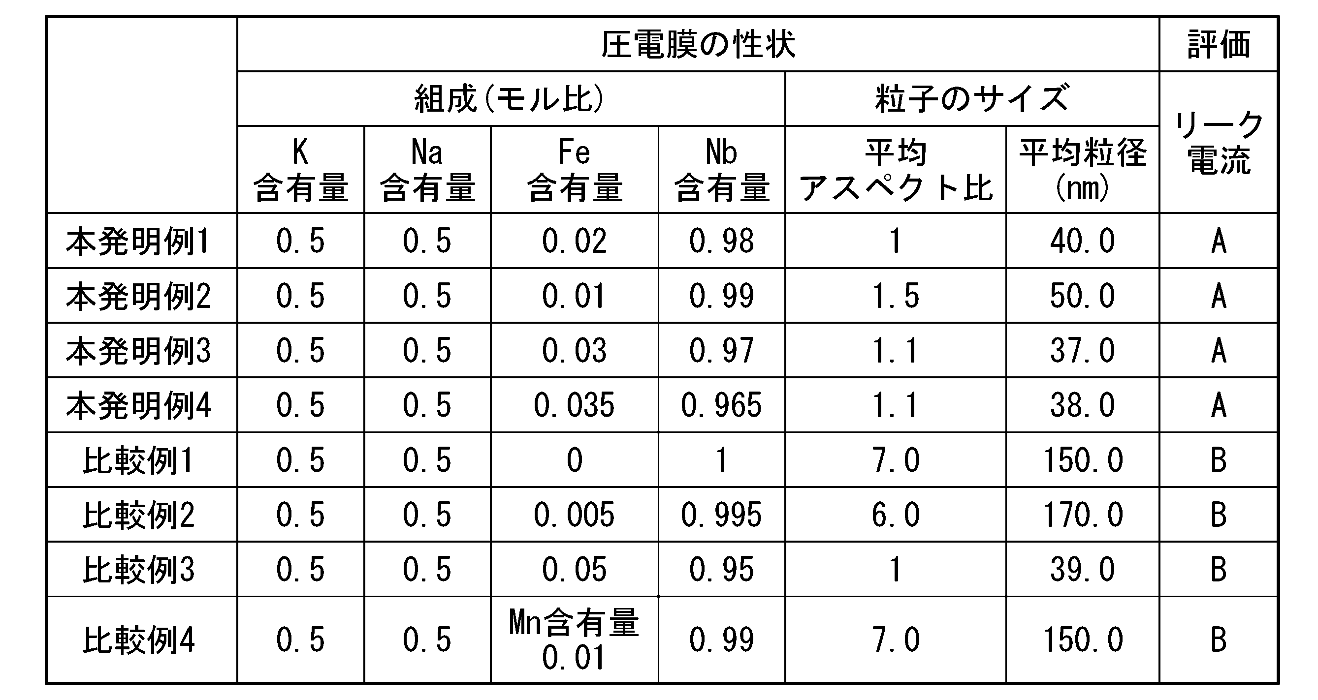
ニオブに対して鉄を本発明の範囲内で含む鉄含有ニオブ酸カリウムナトリウムを用いた本発明例1~4の圧電体膜は、いずれも結晶粒子の平均アスペクト比が3以下であり、リーク電流値が1×10⁻⁵/cm2以下であった。これに対して、Feを含まないニオブ酸カリウムナトリウムを用いた比較例1の圧電体膜は平均アスペクト比が大きく、リーク電流値が1×10-5/cm2を超えていた。また、鉄を本発明の範囲よりも少ない量で含む鉄含有ニオブ酸カリウムナトリウムを用いた比較例2の圧電体膜は、比較例1と比較すると、平均アスペクト比は低くなったが、リーク電流は1×10-5/cm2を超えていた。一方、鉄を本発明の範囲よりも多い量で含む鉄含有ニオブ酸カリウムナトリウムを用いた比較例3の圧電体膜は、平均アスペクト比が1であったが、リーク電流値は1×10-5/cm2を超えていた。これは、鉄が粒界に過剰に存在することによって、リーク電流の発生を抑制することが困難となったためであると考えられる。さらに1モルのニオブに対してマンガンを0.01モル含むマンガン含有ニオブ酸カリウムナトリウムを用いた比較例4の圧電体膜は、平均アスペクト比が7.0と比較例1の圧電体膜の同等であり、リーク電流値は1×10-5/cm2を超えていた。
これらの結果からFeは結晶粒子が柱状に成長することを抑制する作用を有すること、そしてその結晶粒子が、アスペクト比が低い粒状となることによってリーク電流値が低減されることが確認された。
本実施形態のKNN系の圧電体膜および圧電素子は、膜厚を薄くしてもリーク電流が発生しにくい。このため、本実施形態のKNN系の圧電体膜および圧電素子は、振動発電素子、センサ、アクチュエータ、インクジェットヘッド、オートフォーカスなどの様々な圧電デバイスに有利に適用である。
1 圧電素子
10 圧電体膜
11 圧電体層
20 電極層
21 上部電極
22 下部電極
30 粒状結晶粒子
S1、S2 直線
10 圧電体膜
11 圧電体層
20 電極層
21 上部電極
22 下部電極
30 粒状結晶粒子
S1、S2 直線
Claims (3)
- 下記の一般式(1)で表される鉄含有ニオブ酸カリウムナトリウムを含有し、平均アスペクト比が3以下である粒状結晶粒子を含む圧電体膜。
(KxNa1-x)a(FeyNbz)O3・・・(1)
式(1)中、xは、0<x<1を満足する数を表し、aは、0.90<a≦1を満足する数を表し、yとzは、y+z=1で、かつ0.006≦y/z≦0.04を満足する数を表す。 - 前記粒状結晶粒子は、平均粒子径が10nm以上300nm以下の範囲内にある請求項1に記載の圧電体膜。
- 圧電体層と、前記圧電体層の表面に配置されている電極層とを備え、
前記圧電体層は、請求項1または2に記載の圧電体膜を含む圧電素子。
Priority Applications (4)
| Application Number | Priority Date | Filing Date | Title |
|---|---|---|---|
| EP20841144.7A EP3972000A4 (en) | 2019-07-12 | 2020-07-08 | PIEZOELECTRICAL FILM AND PIEZOELECTRICAL ELEMENT |
| US17/617,660 US20220254987A1 (en) | 2019-07-12 | 2020-07-08 | Piezoelectric film and piezoelectric element |
| CN202080049293.6A CN114080696A (zh) | 2019-07-12 | 2020-07-08 | 压电体膜及压电元件 |
| KR1020227000404A KR20220031609A (ko) | 2019-07-12 | 2020-07-08 | 압전체막 및 압전 소자 |
Applications Claiming Priority (2)
| Application Number | Priority Date | Filing Date | Title |
|---|---|---|---|
| JP2019130521A JP7259605B2 (ja) | 2019-07-12 | 2019-07-12 | 圧電体膜および圧電素子 |
| JP2019-130521 | 2019-07-12 |
Publications (1)
| Publication Number | Publication Date |
|---|---|
| WO2021010244A1 true WO2021010244A1 (ja) | 2021-01-21 |
Family
ID=74210711
Family Applications (1)
| Application Number | Title | Priority Date | Filing Date |
|---|---|---|---|
| PCT/JP2020/026652 Ceased WO2021010244A1 (ja) | 2019-07-12 | 2020-07-08 | 圧電体膜および圧電素子 |
Country Status (7)
| Country | Link |
|---|---|
| US (1) | US20220254987A1 (ja) |
| EP (1) | EP3972000A4 (ja) |
| JP (1) | JP7259605B2 (ja) |
| KR (1) | KR20220031609A (ja) |
| CN (1) | CN114080696A (ja) |
| TW (1) | TWI825330B (ja) |
| WO (1) | WO2021010244A1 (ja) |
Cited By (1)
| Publication number | Priority date | Publication date | Assignee | Title |
|---|---|---|---|---|
| WO2022164955A1 (en) * | 2021-01-28 | 2022-08-04 | Kemet Electronics Corporation | Dielectric ceramic composition and ceramic capacitor using the same |
Families Citing this family (1)
| Publication number | Priority date | Publication date | Assignee | Title |
|---|---|---|---|---|
| CN114883476A (zh) * | 2022-05-12 | 2022-08-09 | 业泓科技(成都)有限公司 | 压电元件附着性的改善方法 |
Citations (6)
| Publication number | Priority date | Publication date | Assignee | Title |
|---|---|---|---|---|
| JP2012124354A (ja) * | 2010-12-09 | 2012-06-28 | Seiko Epson Corp | 液体噴射ヘッド、液体噴射装置、及び圧電素子 |
| JP2012121273A (ja) * | 2010-12-09 | 2012-06-28 | Seiko Epson Corp | 液体噴射ヘッド及び液体噴射装置並びに圧電素子 |
| JP2013225605A (ja) * | 2012-04-23 | 2013-10-31 | Seiko Epson Corp | 液体噴射ヘッド及び液体噴射装置並びに圧電素子 |
| WO2015033791A1 (ja) | 2013-09-09 | 2015-03-12 | 株式会社村田製作所 | 圧電薄膜素子及びその製造方法 |
| JP2015534257A (ja) * | 2012-09-21 | 2015-11-26 | Tdk株式会社 | 薄膜圧電素子、圧電アクチュエータ、圧電センサ、ハードディスクドライブおよびインクジェットプリンタ装置 |
| JP2019130521A (ja) | 2018-01-31 | 2019-08-08 | 興研株式会社 | フィルタユニット、フィルタユニットを備えたマスク |
Family Cites Families (7)
| Publication number | Priority date | Publication date | Assignee | Title |
|---|---|---|---|---|
| EP1972607B1 (en) * | 2006-01-12 | 2013-08-14 | Murata Manufacturing Co. Ltd. | Anisotropically shaped ceramic particles and process for production of the same |
| CN101817559B (zh) * | 2010-03-10 | 2012-03-28 | 西安交通大学 | 一种铌酸钾钠无铅压电厚膜的制备方法 |
| CN102959752B (zh) * | 2010-08-12 | 2015-09-02 | 株式会社村田制作所 | 压电薄膜元件的制造方法、压电薄膜元件以及压电薄膜元件用部件 |
| CN102311266B (zh) * | 2011-08-09 | 2013-07-17 | 同济大学 | 一种铌酸钾钠无铅压电陶瓷材料的制备方法 |
| US9065049B2 (en) * | 2012-09-21 | 2015-06-23 | Tdk Corporation | Thin film piezoelectric device |
| US9331262B2 (en) | 2013-05-20 | 2016-05-03 | Tdk Corporation | Thin film piezoelectric element, thin film piezoelectric actuator, thin film piezoelectric sensor, hard drive disk, and inkjet printer device |
| CN105174309A (zh) * | 2015-09-30 | 2015-12-23 | 齐齐哈尔大学 | 一种水热法制备钙钛矿型片状铌酸钾钠的方法 |
-
2019
- 2019-07-12 JP JP2019130521A patent/JP7259605B2/ja active Active
-
2020
- 2020-07-08 US US17/617,660 patent/US20220254987A1/en not_active Abandoned
- 2020-07-08 KR KR1020227000404A patent/KR20220031609A/ko not_active Ceased
- 2020-07-08 EP EP20841144.7A patent/EP3972000A4/en not_active Withdrawn
- 2020-07-08 WO PCT/JP2020/026652 patent/WO2021010244A1/ja not_active Ceased
- 2020-07-08 CN CN202080049293.6A patent/CN114080696A/zh active Pending
- 2020-07-09 TW TW109123154A patent/TWI825330B/zh active
Patent Citations (6)
| Publication number | Priority date | Publication date | Assignee | Title |
|---|---|---|---|---|
| JP2012124354A (ja) * | 2010-12-09 | 2012-06-28 | Seiko Epson Corp | 液体噴射ヘッド、液体噴射装置、及び圧電素子 |
| JP2012121273A (ja) * | 2010-12-09 | 2012-06-28 | Seiko Epson Corp | 液体噴射ヘッド及び液体噴射装置並びに圧電素子 |
| JP2013225605A (ja) * | 2012-04-23 | 2013-10-31 | Seiko Epson Corp | 液体噴射ヘッド及び液体噴射装置並びに圧電素子 |
| JP2015534257A (ja) * | 2012-09-21 | 2015-11-26 | Tdk株式会社 | 薄膜圧電素子、圧電アクチュエータ、圧電センサ、ハードディスクドライブおよびインクジェットプリンタ装置 |
| WO2015033791A1 (ja) | 2013-09-09 | 2015-03-12 | 株式会社村田製作所 | 圧電薄膜素子及びその製造方法 |
| JP2019130521A (ja) | 2018-01-31 | 2019-08-08 | 興研株式会社 | フィルタユニット、フィルタユニットを備えたマスク |
Non-Patent Citations (1)
| Title |
|---|
| See also references of EP3972000A4 |
Cited By (2)
| Publication number | Priority date | Publication date | Assignee | Title |
|---|---|---|---|---|
| WO2022164955A1 (en) * | 2021-01-28 | 2022-08-04 | Kemet Electronics Corporation | Dielectric ceramic composition and ceramic capacitor using the same |
| US11802087B2 (en) | 2021-01-28 | 2023-10-31 | Kemet Electronics Corporation | Dielectric ceramic composition and ceramic capacitor using the same |
Also Published As
| Publication number | Publication date |
|---|---|
| KR20220031609A (ko) | 2022-03-11 |
| EP3972000A1 (en) | 2022-03-23 |
| CN114080696A (zh) | 2022-02-22 |
| JP2021015915A (ja) | 2021-02-12 |
| TW202110746A (zh) | 2021-03-16 |
| TWI825330B (zh) | 2023-12-11 |
| JP7259605B2 (ja) | 2023-04-18 |
| US20220254987A1 (en) | 2022-08-11 |
| EP3972000A4 (en) | 2023-07-19 |
Similar Documents
| Publication | Publication Date | Title |
|---|---|---|
| JP5649316B2 (ja) | 圧電薄膜、圧電素子および圧電素子の製造方法 | |
| JP5903591B2 (ja) | 強誘電体膜、ゾルゲル溶液、成膜方法及び強誘電体膜の製造方法 | |
| US20100025617A1 (en) | Metal oxide | |
| WO2021010244A1 (ja) | 圧電体膜および圧電素子 | |
| JP6787192B2 (ja) | 圧電体膜 | |
| JP6167657B2 (ja) | 強誘電体膜付きシリコン基板 | |
| JP6347085B2 (ja) | 強誘電体膜及びその製造方法 | |
| JP6996019B1 (ja) | スパッタリングターゲット材、及びスパッタリングターゲット材の製造方法 | |
| JP6950404B2 (ja) | 圧電体膜形成用液組成物の製造方法及びこの液組成物を用いて圧電体膜を形成する方法 | |
| JP7464360B2 (ja) | 圧電積層体、圧電素子および圧電積層体の製造方法 | |
| US8237338B2 (en) | Ceramic, and piezoelectric/electrostriction element | |
| JP2020057713A (ja) | 配向性圧電体膜およびその製造方法、圧電体素子、並びに、液体吐出ヘッド | |
| US10770645B2 (en) | Oriented piezoelectric film, method for producing the oriented piezoelectric film, and liquid dispensing head | |
| US10790436B2 (en) | Oriented piezoelectric film and method of manufacturing same, and liquid ejection head | |
| JP7851603B2 (ja) | 積層構造体及びその製造方法、電子デバイス、電子機器並びにシステム | |
| JP2020055716A (ja) | 圧電体膜形成用塗工液組成物、その製造方法、配向性圧電体膜、並びに、液体吐出ヘッド | |
| JP7399753B2 (ja) | 圧電膜、圧電積層体、圧電素子および圧電積層体の製造方法 | |
| WO2012133529A1 (ja) | 圧電体基板の製造方法 | |
| JP7124445B2 (ja) | Bnt-bt系膜及びその形成方法 | |
| JP2020057693A (ja) | 積層圧電体膜 | |
| JP2019167286A (ja) | 圧電体膜形成用液組成物及びこの液組成物を用いて圧電体膜を形成する方法 | |
| US12581862B2 (en) | Piezoelectric film, piezoelectric stack, piezoelectric element, and method of manufacturing piezoelectric stack | |
| JP7230579B2 (ja) | 強誘電体膜の製造方法 | |
| JP2016025142A (ja) | 圧電組成物および圧電素子 | |
| JP2022044257A (ja) | 圧電膜素子及び圧電膜振動子 |
Legal Events
| Date | Code | Title | Description |
|---|---|---|---|
| 121 | Ep: the epo has been informed by wipo that ep was designated in this application |
Ref document number: 20841144 Country of ref document: EP Kind code of ref document: A1 |
|
| ENP | Entry into the national phase |
Ref document number: 2020841144 Country of ref document: EP Effective date: 20211214 |
|
| NENP | Non-entry into the national phase |
Ref country code: DE |