WO2021019964A1 - カレントトランスモジュール - Google Patents
カレントトランスモジュール Download PDFInfo
- Publication number
- WO2021019964A1 WO2021019964A1 PCT/JP2020/024550 JP2020024550W WO2021019964A1 WO 2021019964 A1 WO2021019964 A1 WO 2021019964A1 JP 2020024550 W JP2020024550 W JP 2020024550W WO 2021019964 A1 WO2021019964 A1 WO 2021019964A1
- Authority
- WO
- WIPO (PCT)
- Prior art keywords
- core
- current transformer
- bobbin
- casing
- hollow portion
- Prior art date
- Legal status (The legal status is an assumption and is not a legal conclusion. Google has not performed a legal analysis and makes no representation as to the accuracy of the status listed.)
- Ceased
Links
Images










Classifications
-
- H—ELECTRICITY
- H01—ELECTRIC ELEMENTS
- H01F—MAGNETS; INDUCTANCES; TRANSFORMERS; SELECTION OF MATERIALS FOR THEIR MAGNETIC PROPERTIES
- H01F27/00—Details of transformers or inductances, in general
- H01F27/28—Coils; Windings; Conductive connections
- H01F27/30—Fastening or clamping coils, windings, or parts thereof together; Fastening or mounting coils or windings on core, casing, or other support
- H01F27/306—Fastening or mounting coils or windings on core, casing or other support
-
- H—ELECTRICITY
- H01—ELECTRIC ELEMENTS
- H01F—MAGNETS; INDUCTANCES; TRANSFORMERS; SELECTION OF MATERIALS FOR THEIR MAGNETIC PROPERTIES
- H01F38/00—Adaptations of transformers or inductances for specific applications or functions
- H01F38/20—Instruments transformers
- H01F38/22—Instruments transformers for single phase AC
- H01F38/28—Current transformers
- H01F38/30—Constructions
-
- G—PHYSICS
- G01—MEASURING; TESTING
- G01R—MEASURING ELECTRIC VARIABLES; MEASURING MAGNETIC VARIABLES
- G01R15/00—Details of measuring arrangements of the types provided for in groups G01R17/00 - G01R29/00, G01R33/00 - G01R33/26 or G01R35/00
- G01R15/14—Adaptations providing voltage or current isolation, e.g. for high-voltage or high-current networks
- G01R15/18—Adaptations providing voltage or current isolation, e.g. for high-voltage or high-current networks using inductive devices, e.g. transformers
- G01R15/183—Adaptations providing voltage or current isolation, e.g. for high-voltage or high-current networks using inductive devices, e.g. transformers using transformers with a magnetic core
-
- H—ELECTRICITY
- H01—ELECTRIC ELEMENTS
- H01F—MAGNETS; INDUCTANCES; TRANSFORMERS; SELECTION OF MATERIALS FOR THEIR MAGNETIC PROPERTIES
- H01F27/00—Details of transformers or inductances, in general
- H01F27/02—Casings
-
- H—ELECTRICITY
- H01—ELECTRIC ELEMENTS
- H01F—MAGNETS; INDUCTANCES; TRANSFORMERS; SELECTION OF MATERIALS FOR THEIR MAGNETIC PROPERTIES
- H01F27/00—Details of transformers or inductances, in general
- H01F27/24—Magnetic cores
- H01F27/26—Fastening parts of the core together; Fastening or mounting the core on casing or support
-
- H—ELECTRICITY
- H01—ELECTRIC ELEMENTS
- H01F—MAGNETS; INDUCTANCES; TRANSFORMERS; SELECTION OF MATERIALS FOR THEIR MAGNETIC PROPERTIES
- H01F27/00—Details of transformers or inductances, in general
- H01F27/24—Magnetic cores
- H01F27/26—Fastening parts of the core together; Fastening or mounting the core on casing or support
- H01F27/266—Fastening or mounting the core on casing or support
-
- H—ELECTRICITY
- H01—ELECTRIC ELEMENTS
- H01F—MAGNETS; INDUCTANCES; TRANSFORMERS; SELECTION OF MATERIALS FOR THEIR MAGNETIC PROPERTIES
- H01F27/00—Details of transformers or inductances, in general
- H01F27/28—Coils; Windings; Conductive connections
-
- H—ELECTRICITY
- H01—ELECTRIC ELEMENTS
- H01F—MAGNETS; INDUCTANCES; TRANSFORMERS; SELECTION OF MATERIALS FOR THEIR MAGNETIC PROPERTIES
- H01F27/00—Details of transformers or inductances, in general
- H01F27/28—Coils; Windings; Conductive connections
- H01F27/32—Insulating of coils, windings, or parts thereof
-
- H—ELECTRICITY
- H01—ELECTRIC ELEMENTS
- H01F—MAGNETS; INDUCTANCES; TRANSFORMERS; SELECTION OF MATERIALS FOR THEIR MAGNETIC PROPERTIES
- H01F27/00—Details of transformers or inductances, in general
- H01F27/28—Coils; Windings; Conductive connections
- H01F27/32—Insulating of coils, windings, or parts thereof
- H01F27/324—Insulation between coil and core, between different winding sections, around the coil; Other insulation structures
- H01F27/325—Coil bobbins
-
- H—ELECTRICITY
- H01—ELECTRIC ELEMENTS
- H01F—MAGNETS; INDUCTANCES; TRANSFORMERS; SELECTION OF MATERIALS FOR THEIR MAGNETIC PROPERTIES
- H01F30/00—Fixed transformers not covered by group H01F19/00
- H01F30/06—Fixed transformers not covered by group H01F19/00 characterised by the structure
- H01F30/10—Single-phase transformers
Definitions
- the present invention relates to a current transformer module that detects a current flowing through a device for output control and overcurrent protection operation of various AC devices.
- a current transformer is used to detect the current in high-power electric devices such as air conditioners and IH devices that are operated by a household power supply.
- the current transformer includes a primary coil, a secondary coil, and a core forming a magnetic path common to these coils (see, for example, Patent Document 1).
- a current detection resistor is connected to the secondary coil, the commercial frequency of the power supply of the device is energized in the primary coil, and it is generated according to the current change on the primary side via the magnetic circuit.
- the potential difference between both ends is detected as a voltage as the end resistance for current detection of the next coil.
- the device takes the voltage into a microcomputer and controls an inverter circuit or the like to control the input / output of the device.
- the current transformer is housed in a resin casing and used as a current transformer module. While there is a demand for miniaturization of the current transformer module, it is necessary to secure a creepage distance for insulation between the primary coil and the secondary coil.
- An object of the present invention is to provide a current transformer module capable of simultaneously achieving miniaturization and securing a creepage distance of insulation.
- the current transformer module according to the present invention is It has a hollow portion that penetrates, and includes a resin bobbin in which a primary coil and a secondary coil are wound around the outer periphery of the hollow portion, and at least a core in which a leg is inserted in the hollow portion.
- Current transformer The casing that houses the current transformer and It is a current transformer module that has The bobbin has an insulating wall having a recess between the primary coil and the secondary coil. The casing is formed with a convex portion that fits into the recess.
- the primary side coil is U-shaped
- the secondary side coil is formed by winding a thin winding member
- the casing has a concave contact portion for suppressing the U-shaped primary side coil from coming off. Can be set up.
- the casing is composed of an upper case and a lower case.
- the bobbin is provided with an upper insulating wall having an upper recess at a position facing the upper case and a lower insulating wall having a lower recess at a position facing the lower case.
- the convex portion the upper case may be provided with an upper convex portion that fits into the upper concave portion, and the lower case may be provided with a lower convex portion that fits into the lower concave portion.
- the contact portion can be formed inside the upper surface of the upper case.
- the current transformer module according to the present invention is It has a hollow portion that penetrates, and includes a resin bobbin in which a primary coil and a secondary coil are wound around the outer periphery of the hollow portion, and at least a core in which a leg is inserted in the hollow portion.
- Current transformer The casing that houses the current transformer and It is a current transformer module equipped with The core is arranged with play in the penetrating direction of the hollow portion.
- the casing accommodates the bobbin in a positionable manner and accommodates the core in a positionable manner, so that the bobbin and the core are relatively positioned.
- one inner surface intersecting the penetrating direction of the hollow portion of the bobbin is in contact with the core and is formed parallel to the outer peripheral surface of the core, and the core is in contact with the inner surface to face the core. Is pressed against the bobbin, so that the core can be positioned on the bobbin.
- the bobbin has an insulating wall having a recess between the primary coil and the secondary coil.
- the casing is formed with a convex portion that fits into the recess. By fitting the convex portion into the recess, the bobbin can be configured to be positioned on the casing.
- the core can be configured to be positioned on the casing by abutting on the inner surface of the casing.
- the current transformer module of the present invention can achieve miniaturization of the bobbin and the current transformer module while ensuring the creepage distance of insulation between the primary side coil and the secondary side coil by the bobbin and casing of the current transformer.
- the bobbin and the core can be relatively positioned by positioning the bobbin and the core of the current transformer in the casing, respectively.
- FIG. 1 is a perspective view of a current transformer according to an embodiment of the present invention.
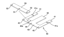
- FIG. 2 is an exploded perspective view of a core component for a current transformer of the present invention.
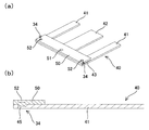
- FIG. 3 is a perspective view (a) and a cross-sectional view (b) of a core component for a current transformer in which an E-type core and an I-type core are integrated by caulking.
- FIG. 4 is a perspective view of an embodiment without a pilot hole, which is a core component for a current transformer in which an E-type core and an I-type core are integrated by caulking.
- FIG. 1 is a perspective view of a current transformer according to an embodiment of the present invention.
- FIG. 2 is an exploded perspective view of a core component for a current transformer of the present invention.
- FIG. 3 is a perspective view (a) and a cross-sectional view (b) of a core component for a current transformer in which an E-type core and an I-type core are integrated by caul
- FIG. 5 is a perspective view of a core component for a current transformer in which an E-type core and an I-type core are integrated by welding, in which (a) is an edge and (b) is a side surface welded. ..
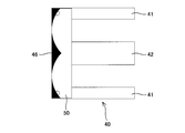
- FIG. 6 is a plan view showing a region where the magnetic flux density is low when the core component for the current transformer is incorporated in the current transformer.
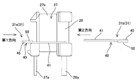
- FIG. 7 is a side view showing a process of inserting a core component for a current transformer into a bobbin around which a primary coil and a secondary coil are wound.
- FIG. 8 is a vertical cross-sectional view showing a process of inserting a core component for a current transformer into the bobbin.
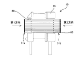
- FIG. 10 shows a step of adjusting a gap formed between a core component for a current transformer inserted and integrated from the first direction and a core component for a current transformer inserted and integrated from the second direction. It is a side view.
- FIG. 11 shows a state in which the core component for the current transformer inserted and integrated from the first direction and the core component for the current transformer inserted and integrated from the second direction are integrated by spot welding after adjusting the gap. It is a side view which shows.
- FIG. 12 is a side view showing an embodiment in which the core component for a current transformer inserted from the first direction and the core component for a current transformer inserted from the second direction are integrated after adjusting the gap.
- FIG. 13 is a side view showing an embodiment in which the front and back stacking order is changed when stacking the core components for the current transformer.
- FIG. 14 is an enlarged view of a butt portion of an E-type core and an I-type core (both manufactured by press punching) facing each other with a gap in between, and FIG. 14A is an enlarged view of shear sections and fracture surfaces abutted against each other.
- An embodiment, (b) shows an embodiment in which a shear section and a fracture surface are butted against each other.
- FIG. 15 is a perspective view showing a manufacturing mode of a current transformer in which a core component for a current transformer inserted from the first direction and a core component for a current transformer inserted from the second direction are each previously blocked and inserted into a bobbin.
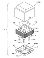
- FIG. 16 is an exploded view of the current transformer module according to the embodiment of the present invention.
- FIG. 17 is a perspective view of the current transformer module.
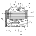
- FIG. 18 is a cross-sectional view of the current transformer module.
- FIG. 19 is a bottom view of the upper case.
- FIG. 20 is a plan view of the lower case.
- core component the current transformer core component 31 (hereinafter referred to as “core component”), the current transformer 10, and the current transformer module 12 according to the embodiment of the present invention will be described with reference to the drawings.
- FIG. 1 is a perspective view of a current transformer 10 according to an embodiment of the present invention.
- the current transformer 10 has a common magnetic path of the primary coil 26 and the secondary coil 27 on the resin bobbin 20 around which the primary coil 26 and the secondary coil 27 are wound. It is configured by mounting the core 30 forming the above.
- the primary side coil 26 is a U-shaped winding member
- the secondary side coil 27 is a thin winding member wound around the bobbin 20, and the outer circumference is protected by tape. There is.
- the core 30 is configured by laminating a plurality of core parts 31.
- FIG. 2 is an exploded perspective view of one core component 31 constituting the core 30.
- the core component 31 can be composed of an E-type core 40 and an I-type core 50.
- the E-type core 40 and the I-type core 50 can be obtained by press-punching an electromagnetic steel sheet such as a silicon steel sheet. For example, a thin strip-shaped electromagnetic steel plate can be adopted.
- the E-shaped core 40 includes three substantially rectangular legs 41, 42, 41 extending substantially in parallel and a substantially rectangular connecting portion 43 connecting one ends of these legs 41, 42, 41. It is desirable that the width dimension 43a of the connecting portion 43 is longer than the width dimension 41a of the leg portion 41 in order to suppress the leakage flux. Further, the I-type core 50 can have a substantially rectangular shape having substantially the same size as the connecting portion 43. It is desirable that the E-type core 40 and the I-type core 50 have pilot holes 44 and 51 for positioning. Further, in order to align the I-type core 50 with the E-type core 40 and facilitate stacking, the length-wise dimension of the I-type core 50 is smaller than the longitudinal dimension of the connecting portion 43 of the E-type core 40. It is desirable to reduce the size by 1 mm to 0.3 mm.
- the E-type core 40 and the I-type core 50 form a core component 31 by superimposing the I-type core 50 on the connecting portion 43 of the E-type core 40 and integrating them.
- Examples of the integration include caulking 34 shown in FIGS. 3 and 4, welding 35 shown in FIG. 5, and adhesion (not shown).
- a caulking hole 45 is formed in advance in one of the E-type core 40 or the I-type core 50 and a dowel 52 is formed in the other as shown in FIG. , As shown in FIGS. 3A and 3B, the E-type core 40 and the I-type core 50 may be overlapped and the caulking holes 45 and the dowels 52 may be aligned to perform the caulking 34.
- the caulking hole 45 can be formed at the same time when the E-type core 40 and the I-type core 50 are pressed and punched. When the caulking hole 45 is formed, it is desirable that the caulking hole 45 is formed in the E-shaped core 40 having a large area in order to suppress a decrease in strength or deformation of the core 30.
- FIG. 5 the outer edge of the connecting portion 43 of the E-type core 40 and the outer edge of the I-type core 50 are shown in FIG. 5 (a). Welding may be performed so as to straddle. Further, as shown in FIG. 5B, welding 35 may be performed so as to straddle both ends of the connecting portion 43 of the E-type core 40 and both ends of the I-type core 50. Welding 35 can exemplify laser welding, laser welding, and resistance welding (the same applies to welding according to the following description), but is not limited thereto.
- welding 35 is performed in the region 46 having a low magnetic flux density among the core parts 31, that is, in the corners and the center near the outer edge of the E-type core 40 and the I-type core 50. Is desirable. Since the region 46 is a region where the magnetic flux density is low even in the magnetic path, the influence on the performance can be suppressed even if the magnetic characteristics are slightly deteriorated.
- a plurality of core components 31 formed by integrating the E-type core 40 and the I-type core 50 are prepared (current transformer core component preparation step), and the core component 31 is mounted on the bobbin 20. ..
- the bobbin 20 is wound with a U-shaped primary coil 26 and a secondary coil 27 whose outer circumference is protected by tape 27b, and the bobbin 20 is orthogonal to these coils 26 and 27.
- a hollow portion 21 having a penetrating direction is prepared (bobbin preparation step).
- the core component 31 is laminated by sequentially inserting the central leg portion 42 into the hollow portion 21 of the bobbin 20. Specifically, as shown in the figure, the core parts 31 and 31 are alternately inserted into the hollow portion 21 in the opposite directions.
- the first core component 31 With the I-type core 50 facing upward, the legs 41, 42, 41 of the E-type core 40 facing the bobbin 20 side from the first direction, and the bobbin so that the central leg 42 is inserted into the hollow portion 21.
- the central leg portion 42 is inserted into the hollow portion 21 by approaching 20.
- the I-type core 50 faces downward
- the legs 41, 42, 41 of the E-type core 40 face the bobbin 20 side from the second direction
- the central leg 42 The bobbin 20 is approached so as to be inserted into the hollow portion 21, the central leg portion 42 is inserted into the hollow portion 21, and the legs 41, 42, 41 of the first core component 31 and the second core component 31 are inserted.
- the legs 41, 42, 41 of the above are overlapped.
- the core component inserted from the first direction will be referred to as a first core component 31a
- the core component inserted from the second direction will be referred to as a second core component 31b.
- the first core component 31a and the second core component 31b become the leg portion 41 as shown in FIG. , 42 (42 is not shown) are laminated in a stacked state (lamination step).
- the current transformer 10 can be obtained by this, but in this state, the first core component 31a and the second core component 31b are not fixed or the like, and are still inserted into the hollow portion 21. Therefore, as shown in FIG. 9, the first core parts 31a and the second core parts 31b are integrated with each other by aligning the edges so that the laminated first core parts 31a and the second core parts 31b do not come apart. It is desirable to do (integration step).
- the integration can be, for example, welding as shown by reference numeral 36 in FIG. Welding 36 can be exemplified by laser welding and resistance welding. In addition, it may be integrated by caulking or adhesive. When welding 36 is performed, it is desirable to perform welding in the region 46 having a low magnetic flux density described with reference to FIG.
- the tips of the legs 41, 42, 41 of the first core component 31a and the I-type core of the second core component 31b A gap 60 is formed between the 50 and the inner edge of the 50. Further, a gap 60 is formed between the tips of the legs 41, 42, 41 of the second core component 31b and the inner edge of the I-shaped core 50 of the first core component 31a.
- the gap 60 can be adjusted by pushing the first core component 31a and the second core component 31b from the first direction and the second direction (gap adjustment step).
- the tolerance can be made as small as possible. According to the present invention, the tolerance can be ⁇ 1% or less, preferably ⁇ 0.5% or less in terms of actual value.
- the gap 60 can be 0.1 mm to 0.4 mm, preferably about 0.2 mm.
- the first core component 31a and the second core component 31b are welded 37 at the overlapping positions of the legs 41 and 41 located on the outer side. Integrate by means of etc. (integration step). As a result, the first core component 31a and the second core component 31b are integrated, and it is possible to prevent the gap 60 once adjusted from changing in width. Since the first core component 31a and the second core component 31b are integrated first, the welding 37 for integrating the first core component 31a and the second core component 31b is performed at one or a plurality of locations. Only spot welding is required. Therefore, the welding 37 has almost no effect on the magnetic characteristics of the core parts 31a and 31b.
- the first core component 31a and the second core component 31b can be integrated without using a varnish, an adhesive, or a resin, so that they are not affected by thermal expansion and contraction. Therefore, it is possible to provide a current transformer 10 having excellent temperature characteristics.
- the first core component 31a and the second core component 31b are integrated with each other, and then the gap 60 is adjusted to integrate the first core component 31a and the second core component 31b. ..
- the welding 36 of FIG. 9 may be omitted, and the gap 60 may be adjusted without integrating the first core parts 31a and the second core parts 31b.
- the overlapping positions of the legs 41 and 41 located outside the first core component 31a and the second core component 31b may be line-welded 38 as shown in FIG.
- the manufacturing process of the current transformer 10 can be simplified.
- the first core component 31a and the second core component 31b are welded 37, 38 at the substantially central portion of the leg portion 41 of the E-shaped core 40. Therefore, the length of the linear expansion is suppressed to half, and the first core component 31a and the second core component 31b linearly expand in the same direction starting from the welded portions 37 and 38, so that the gap 60 does not change substantially. Further, since the welded portions 36 and 37 in FIG. 11 and the welded portions 38 in FIG. 12 are formed substantially parallel to the stacking direction of the first core component 31a and the second core component 31b, the lines due to the heat of these welded portions are formed. Expansion does not affect the size of the gap 60.
- all the first core parts 31a are stacked with the I-type core 50 facing upward, and all the second core parts 31b are stacked facing downward.
- the first core part 31a and the first core component 31a As long as the two core parts 31b are paired, the front and back sides may be changed alternately, for each of a plurality of pairs, or even randomly. As a result, it is possible to equalize the variation in thickness due to the burrs 73 and the drool 70 (see FIG. 14) when the E-type core 40 and the I-type core 50 are manufactured by press punching.
- the E-type core 40 and the I-type core 50 are arranged so that the shear sections 71 and 71 and the fracture surfaces 72 and 72 face each other, and the fracture surfaces 72 and 72 are butted against each other. Then, the fracture surfaces 72 and 72 come into contact with each other, but a gap remains between the shear sections 71 and 71. Therefore, the adjustment range of the gap becomes small, and the adjustment range of the output voltage also becomes narrow. Therefore, when the E-type core 40 and the I-type core 50 are butted against each other, as shown in FIG. 14B, the E-type core 40 and the I-type core 50 have a shear section 71 and a fracture surface 72 facing each other. It is desirable to arrange them in such a manner. As a result, the gap 60 can be reduced, so that the adjustment range of the gap 60 can be widened to widen the adjustment range of the output voltage, and the adjustment can be easily performed.
- the first core component 31a and the second core component 31b are inserted into the hollow portion 21 one by one.
- the first core component block 32a and the second core component 31b in which the first core component 31a is laminated in advance and integrated by welding or caulking, are laminated in advance and integrated by welding or caulking.
- the second core component block 32b is created and mounted on the bobbin 20
- the legs 41 and the second core component of the second core component 31b are sandwiched between the legs 41 and 41 of the first core components 31a and 31a.
- the legs 41 of the first core component 31a may be engaged so as to enter between the legs 41 and 41 of the 31b and 31b.
- the core parts 31a and 31b do not need to be laminated one by one on the bobbin 20, so that the manufacturing process can be simplified as much as possible.
- the current transformer 10 obtained as described above can be housed in the casing 80 and used as the current transformer module 12.
- 16 is an exploded perspective view of the current transformer 10 and the casing 80 accommodating the current transformer 10
- FIG. 17 is a perspective view of the current transformer 10
- FIG. 18 is a vertical sectional view of the current transformer 10.
- the casing 80 is formed from an upper case 81 and a lower case 85.
- the upper case 81 has an open housing shape on the lower surface for accommodating the core 30 and the bobbin 20
- the lower case 85 has a plate shape on which the bobbin 20 is placed and closes the lower surface of the upper case 81. it can.
- FIG. 19 shows a bottom view of the upper case 81
- FIG. 20 shows a plan view of the lower case 85.
- the lower case 85 is formed with insertion holes 86a and 86b into which the terminal wires 26a and 26a of the primary coil 26 and the terminal wires 27a and 27a of the secondary coil 27 are extended, respectively.
- the current transformer module 12 can be obtained by inserting the terminal wires 26a and 26b into the insertion holes 86a and 86b and fitting the upper case 81 with the bobbin 20 positioned in the lower case 85. The obtained current transformer module 12 is shown in FIG.
- the output voltage characteristics can be measured individually, and the obtained characteristic data can be printed or sealed on the upper case 81 as a data matrix 89 as shown in FIG.
- the data matrix 89 can be read and the characteristic adjustment can be performed on the control based on the corresponding characteristic data. As a result, more accurate output voltage characteristics can be achieved.
- the bobbin 20 has an upper insulating wall 22 and a primary coil 26 provided between the primary coil 26 and the secondary coil 27.
- An upper concave portion 23 is formed between them, while an upper convex portion 83 that fits into the upper concave portion 23 is formed in the upper case 81 as shown in FIGS. 18 and 19.
- the upper convex portion 83 fits into the upper recess 23 to form an insulating wall, and the creepage distance between the insulation of the primary coil 26 and the secondary coil 27 is increased. I try to earn a long time. Further, the bobbin 20 can be positioned on the upper case 81 by fitting the upper convex portion 83 into the upper concave portion 23.
- a recess is formed along the outer shape of the primary coil 26 as a contact portion 82 for suppressing the primary coil 26 from coming off.
- the contact portion 82 prevents the primary coil 26 from floating when the current transformer module 12 is mounted on a printed wiring board or the like.
- the bobbin 20 has a lower recess 25 between the lower insulating wall 24 provided between the primary coil 26 and the secondary coil 27 and the primary coil 26.
- the lower case 85 is formed with a lower convex portion 87 that fits into the lower recess 25.
- the lower convex portion 87 fits into the lower recess 25 and becomes an insulating wall to insulate the primary coil 26 and the secondary coil 27. I am trying to earn a long creepage distance.
- the current transformer 10 and the current transformer module 12 can be downsized by lowering the insulating walls 22 and 24 of the bobbin 20 while ensuring the creepage distance between the primary coil 26 and the secondary coil 27. Further, the bobbin 20 can be positioned on the lower case 85 by fitting the lower convex portion 87 into the lower recess 25.
- the lower case 85 is provided with a step portion 88 that supports the lower surface of the bobbin 20, and when the bobbin 20 comes into contact with the lower case 85, the lower surface of the bobbin 20 is brought into contact with the step portion 88, and the bobbin 20 is the casing 80. It is desirable to hold it without tilting inside.
- the core 30 since the gap 60 is adjusted with reference to the output voltage characteristic, the core 30 has a play in the longitudinal direction of the leg 41 with respect to the bobbin 20 due to the width of the gap 60. It will be held, and may slide in the penetrating direction of the hollow portion 21 to cause play. Therefore, in the current transformer module 12, it is desirable to position the core 30 with respect to the bobbin 20.
- the bobbin 20 is positioned on the casing 80 by fitting the upper concave portion 23 and the upper convex portion 83, and fitting the lower concave portion 25 and the lower convex portion 87. Therefore, if the core 30 can also be positioned with respect to the casing 80, the core 30 and the bobbin 20 can also be positioned relative to each other. Therefore, in the present embodiment, as shown in FIG. 18, a structure capable of positioning the core 30 with respect to the casing 80 is adopted.
- the core 30 is composed of a first core component 31a and a second core component 31b in which an E-type core 40 and an I-type core 50 are integrated, respectively, but the current transformer 10 is not limited thereto. Absent.
Landscapes
- Engineering & Computer Science (AREA)
- Power Engineering (AREA)
- Physics & Mathematics (AREA)
- General Physics & Mathematics (AREA)
- Transformers For Measuring Instruments (AREA)
- Coils Or Transformers For Communication (AREA)
Abstract
Description
貫通した中空部を有し、前記中空部の外周に1次側コイルと2次側コイルを巻線した樹脂製のボビンと、少なくとも前記中空部に脚部が挿入されたコアと、を具える、カレントトランスと、
前記カレントトランスを収容するケーシングと、
を具えるカレントトランスモジュールであって、
前記ボビンは、前記1次側コイルと前記2次側コイルとの間に凹みを有する絶縁壁を有しており、
前記ケーシングは、前記凹みに嵌合する凸部が形成されている。
前記絶縁壁として、前記ボビンには、前記上ケースと対向する位置に上側凹みを有する上側絶縁壁、前記下ケースと対向する位置に下側凹みを有する下側絶縁壁を具え、
前記凸部として、前記上ケースには、前記上側凹みに嵌合する上側凸部、前記下ケースには、前記下側凹みに嵌合する下側凸部を具える構成とすることができる。
貫通した中空部を有し、前記中空部の外周に1次側コイルと2次側コイルを巻線した樹脂製のボビンと、少なくとも前記中空部に脚部が挿入されたコアと、を具える、カレントトランスと、
前記カレントトランスを収容するケーシングと、
を具えるカレントトランスモジュールであって、
前記コアは、前記中空部の貫通方向に遊びをもって配置されており、
前記ケーシングは、前記ボビンを位置決め可能に収容すると共に、前記コアを位置決め可能に収容し、前記ボビンと前記コアが相対的に位置決めされる。
前記ケーシングは、前記凹みに嵌合する凸部が形成されており、
前記凹みに前記凸部が嵌合することで、前記ボビンは前記ケーシングに位置決めされる構成とすることができる。
上記実施形態では、第1コア部品31a、第2コア部品31bを1枚ずつ中空部21に挿入している。しかしながら、たとえば、図15に示すように、第1コア部品31aを予め積層して溶接やカシメにより一体化した第1コア部品ブロック32a、第2コア部品31bを予め積層して溶接やカシメにより一体化した第2コア部品ブロック32bを夫々作成し、ボビン20に装着する際に、第1コア部品31a,31aの脚部41,41間に第2コア部品31bの脚部41、第2コア部品31b、31bの脚部41,41間に第1コア部品31aの脚部41が侵入するよう噛み合わせてもよい。これにより、コア部品31a,31bはボビン20で1枚ずつ積層する必要はないから製造工程を可及的に簡便化することができる。
11 カレントトランスモジュール
20 ボビン
21 中空部
22 上側絶縁壁
23 上側凹み
24 下側絶縁壁
25 下側凹み
30 コア
80 ケーシング
81 上ケース
83 上側凸部
84 内面
85 下ケース
87 下側凸部
Claims (4)
- 貫通した中空部を有し、前記中空部の外周にU字状の1次側コイルと細巻線部材を巻回してなる2次側コイルを巻線した樹脂製のボビンと、少なくとも前記中空部に脚部が挿入されたコアと、を具える、カレントトランスと、
前記カレントトランスを収容するケーシングと、
を具えるカレントトランスモジュールであって、
前記ボビンは、前記1次側コイルと前記2次側コイルとの間に凹みを有する絶縁壁を有し、
前記ケーシングは、前記凹みに嵌合する凸部が形成されると共に、前記U字状の1次側コイルの抜けを抑える当たり部が凹設されている、
カレントトランスモジュール。 - 前記ケーシングは、上ケースと下ケースから構成され、
前記絶縁壁として、前記ボビンには、前記上ケースと対向する位置に上側凹みを有する上側絶縁壁、前記下ケースと対向する位置に下側凹みを有する下側絶縁壁を具え、
前記凸部として、前記上ケースには、前記上側凹みに嵌合する上側凸部、前記下ケースには、前記下側凹みに嵌合する下側凸部を具え、
前記当たり部は、前記上ケースの上面内側に形成される、
請求項1に記載のカレントトランスモジュール。 - 貫通した中空部を有し、前記中空部の外周に1次側コイルと2次側コイルを巻線した樹脂製のボビンと、少なくとも前記中空部に脚部が挿入されたコアと、を具える、カレントトランスと、
前記カレントトランスを収容するケーシングと、
を具えるカレントトランスモジュールであって、
前記コアは、前記中空部の貫通方向に遊びをもって配置されており、
前記ケーシングは、前記ボビンを位置決め可能に収容すると共に、前記ケーシングは、前記ボビンの前記中空部の貫通方向と交差する一方の内面が前記コアと当接し、前記コアの外周面と平行に形成され、前記コアは前記内面に面当たりして、前記コアが前記ボビンに押し当てられることで、前記ボビンに前記コアを位置決めしている、
カレントトランスモジュール。 - 前記ボビンは、前記1次側コイルと前記2次側コイルとの間に凹みを有する絶縁壁を有し、
前記ケーシングは、前記凹みに嵌合する凸部が形成されており、
前記凹みに前記凸部が嵌合することで、前記ボビンは前記ケーシングに位置決めされる、
請求項3に記載のカレントトランスモジュール。
Priority Applications (4)
| Application Number | Priority Date | Filing Date | Title |
|---|---|---|---|
| KR1020227002946A KR102731474B1 (ko) | 2019-07-31 | 2020-06-23 | 변류기 모듈 |
| EP20847599.6A EP4006930B1 (en) | 2019-07-31 | 2020-06-23 | Current transformer module |
| US17/630,410 US12525392B2 (en) | 2019-07-31 | 2020-06-23 | Current transformer module |
| CN202080054948.9A CN114144856B (zh) | 2019-07-31 | 2020-06-23 | 电流互感器模块 |
Applications Claiming Priority (2)
| Application Number | Priority Date | Filing Date | Title |
|---|---|---|---|
| JP2019140980A JP6647723B1 (ja) | 2019-07-31 | 2019-07-31 | カレントトランスモジュール |
| JP2019-140980 | 2019-07-31 |
Publications (1)
| Publication Number | Publication Date |
|---|---|
| WO2021019964A1 true WO2021019964A1 (ja) | 2021-02-04 |
Family
ID=69568134
Family Applications (1)
| Application Number | Title | Priority Date | Filing Date |
|---|---|---|---|
| PCT/JP2020/024550 Ceased WO2021019964A1 (ja) | 2019-07-31 | 2020-06-23 | カレントトランスモジュール |
Country Status (7)
| Country | Link |
|---|---|
| US (1) | US12525392B2 (ja) |
| EP (1) | EP4006930B1 (ja) |
| JP (1) | JP6647723B1 (ja) |
| KR (1) | KR102731474B1 (ja) |
| CN (1) | CN114144856B (ja) |
| TW (1) | TWI823013B (ja) |
| WO (1) | WO2021019964A1 (ja) |
Families Citing this family (1)
| Publication number | Priority date | Publication date | Assignee | Title |
|---|---|---|---|---|
| JP6679061B1 (ja) | 2020-02-07 | 2020-04-15 | 株式会社エス・エッチ・ティ | カレントトランスモジュール |
Citations (9)
| Publication number | Priority date | Publication date | Assignee | Title |
|---|---|---|---|---|
| JPS4961012U (ja) * | 1972-09-06 | 1974-05-29 | ||
| JPS5186535U (ja) * | 1974-12-30 | 1976-07-10 | ||
| JPS6318824U (ja) | 1986-07-23 | 1988-02-08 | ||
| JPH03227004A (ja) * | 1990-01-31 | 1991-10-08 | Matsushita Electric Ind Co Ltd | カレントトランス |
| JPH0644117U (ja) * | 1992-11-18 | 1994-06-10 | 松下電器産業株式会社 | トランス |
| JPH06302438A (ja) * | 1993-04-12 | 1994-10-28 | Matsushita Electric Ind Co Ltd | トランス |
| JP2004319663A (ja) * | 2003-04-15 | 2004-11-11 | Sht Corp Ltd | カレントトランス |
| JP2007281190A (ja) * | 2006-04-06 | 2007-10-25 | Sanken Electric Co Ltd | 巻線装置とその組立法 |
| JP2014236128A (ja) * | 2013-06-03 | 2014-12-15 | Tdk株式会社 | コイル装置 |
Family Cites Families (22)
| Publication number | Priority date | Publication date | Assignee | Title |
|---|---|---|---|---|
| JPS4961012A (ja) | 1972-05-24 | 1974-06-13 | ||
| JPS5186535A (ja) | 1975-01-25 | 1976-07-29 | Toyota Motor Co Ltd | Suiseitoryonotosohoho |
| JPS6318824A (ja) | 1986-07-11 | 1988-01-26 | Nippon Telegr & Teleph Corp <Ntt> | 2ピ−ス形携帯無線電話機 |
| JP3394270B2 (ja) | 1992-04-16 | 2003-04-07 | 日本電気株式会社 | リカバリ用ジャーナル管理方式 |
| JP2770938B2 (ja) * | 1995-03-08 | 1998-07-02 | サンデン株式会社 | 電磁装置 |
| JPH11297535A (ja) * | 1998-04-14 | 1999-10-29 | Tamura Seisakusho Co Ltd | カバー付小型トランス |
| JP3440853B2 (ja) * | 1998-11-20 | 2003-08-25 | 松下電器産業株式会社 | トランス |
| JP2001244111A (ja) * | 2000-02-29 | 2001-09-07 | Sanden Corp | コイルボビン |
| JP2001332418A (ja) * | 2000-05-23 | 2001-11-30 | Sanden Corp | コイルボビン |
| JP3476077B2 (ja) * | 2000-08-21 | 2003-12-10 | 株式会社タムラ製作所 | カレントトランス用コイルボビンおよびその製造方法 |
| CN2639896Y (zh) * | 2003-07-29 | 2004-09-08 | 台达电子工业股份有限公司 | 电流感应模块 |
| JP2008010660A (ja) * | 2006-06-29 | 2008-01-17 | Kowa Denshi Kogyo Kk | 零相変流器 |
| CN101901661B (zh) * | 2009-05-26 | 2011-12-21 | 浙江三花股份有限公司 | 一种电磁线圈装置 |
| TW201113913A (en) * | 2009-10-15 | 2011-04-16 | Delta Electronics Inc | Transformer structure |
| TWI371764B (en) * | 2009-11-17 | 2012-09-01 | Delta Electronics Inc | Current transformer structure |
| KR20120007130U (ko) * | 2011-04-07 | 2012-10-17 | 김용현 | 계기용 변류기 |
| CN203325703U (zh) * | 2013-07-19 | 2013-12-04 | 范宗爱 | 电流互感器 |
| HUE044015T2 (hu) * | 2014-01-28 | 2019-09-30 | Soc Es De Electromedicina Y Calidad S A | Nagyfeszültségû, nagyfrekvenciájú, nagyteljesítményû transzformátor |
| CN204011030U (zh) * | 2014-08-20 | 2014-12-10 | 南京智达电气有限公司 | 中压浇注式电流互感器 |
| CN205789475U (zh) * | 2016-05-13 | 2016-12-07 | 南京新联电子股份有限公司 | 一种开口式电流互感器 |
| JP2018163952A (ja) * | 2017-03-24 | 2018-10-18 | Fdk株式会社 | カレントトランス |
| WO2020092636A1 (en) * | 2018-11-01 | 2020-05-07 | Bourns, Inc. | Low-profile housing for electronic components |
-
2019
- 2019-07-31 JP JP2019140980A patent/JP6647723B1/ja active Active
-
2020
- 2020-06-23 KR KR1020227002946A patent/KR102731474B1/ko active Active
- 2020-06-23 US US17/630,410 patent/US12525392B2/en active Active
- 2020-06-23 CN CN202080054948.9A patent/CN114144856B/zh active Active
- 2020-06-23 EP EP20847599.6A patent/EP4006930B1/en active Active
- 2020-06-23 WO PCT/JP2020/024550 patent/WO2021019964A1/ja not_active Ceased
- 2020-07-06 TW TW109122762A patent/TWI823013B/zh active
Patent Citations (9)
| Publication number | Priority date | Publication date | Assignee | Title |
|---|---|---|---|---|
| JPS4961012U (ja) * | 1972-09-06 | 1974-05-29 | ||
| JPS5186535U (ja) * | 1974-12-30 | 1976-07-10 | ||
| JPS6318824U (ja) | 1986-07-23 | 1988-02-08 | ||
| JPH03227004A (ja) * | 1990-01-31 | 1991-10-08 | Matsushita Electric Ind Co Ltd | カレントトランス |
| JPH0644117U (ja) * | 1992-11-18 | 1994-06-10 | 松下電器産業株式会社 | トランス |
| JPH06302438A (ja) * | 1993-04-12 | 1994-10-28 | Matsushita Electric Ind Co Ltd | トランス |
| JP2004319663A (ja) * | 2003-04-15 | 2004-11-11 | Sht Corp Ltd | カレントトランス |
| JP2007281190A (ja) * | 2006-04-06 | 2007-10-25 | Sanken Electric Co Ltd | 巻線装置とその組立法 |
| JP2014236128A (ja) * | 2013-06-03 | 2014-12-15 | Tdk株式会社 | コイル装置 |
Non-Patent Citations (1)
| Title |
|---|
| See also references of EP4006930A4 |
Also Published As
| Publication number | Publication date |
|---|---|
| CN114144856B (zh) | 2024-12-27 |
| US20220285090A1 (en) | 2022-09-08 |
| EP4006930B1 (en) | 2026-01-28 |
| JP2021027066A (ja) | 2021-02-22 |
| TWI823013B (zh) | 2023-11-21 |
| TW202109568A (zh) | 2021-03-01 |
| KR102731474B1 (ko) | 2024-11-15 |
| US12525392B2 (en) | 2026-01-13 |
| EP4006930A1 (en) | 2022-06-01 |
| JP6647723B1 (ja) | 2020-02-14 |
| CN114144856A (zh) | 2022-03-04 |
| EP4006930A4 (en) | 2023-11-15 |
| KR20220038359A (ko) | 2022-03-28 |
Similar Documents
| Publication | Publication Date | Title |
|---|---|---|
| KR100413386B1 (ko) | 고주파 대전류변압기 | |
| KR101525748B1 (ko) | 전원공급장치 | |
| US7646281B2 (en) | Snap-together choke and transformer assembly for an electric arc welder | |
| KR102815869B1 (ko) | 변류기 및 변류기의 제조 방법 | |
| JPH0722258A (ja) | リアクタ及びその製造方法 | |
| JP2000077242A (ja) | 電磁機器 | |
| KR102731474B1 (ko) | 변류기 모듈 | |
| JP4845199B2 (ja) | トランス | |
| KR870003870Y1 (ko) | 변압기 | |
| JP2009105180A (ja) | トランス | |
| CN109659118B (zh) | 电抗器 | |
| JP4783516B2 (ja) | インバータトランス | |
| KR20170137630A (ko) | 전자 유도기 및 전자 유도기의 제조 방법 | |
| JP2011103365A (ja) | リアクトル | |
| JPH07235432A (ja) | 変圧器用コイルボビン | |
| JP3082498U (ja) | 漏れ電流低減用絶縁トランス | |
| JP2009246239A (ja) | リアクトル及びコイル成形体 | |
| JP2005072261A (ja) | 低背型トランスの製造方法および低背型トランス |
Legal Events
| Date | Code | Title | Description |
|---|---|---|---|
| 121 | Ep: the epo has been informed by wipo that ep was designated in this application |
Ref document number: 20847599 Country of ref document: EP Kind code of ref document: A1 |
|
| NENP | Non-entry into the national phase |
Ref country code: DE |
|
| ENP | Entry into the national phase |
Ref document number: 2020847599 Country of ref document: EP Effective date: 20220228 |
|
| WWG | Wipo information: grant in national office |
Ref document number: 202080054948.9 Country of ref document: CN |
|
| WWG | Wipo information: grant in national office |
Ref document number: 17630410 Country of ref document: US |
|
| WWG | Wipo information: grant in national office |
Ref document number: 2020847599 Country of ref document: EP |