WO2021020152A1 - コネクタ及び電子機器 - Google Patents
コネクタ及び電子機器 Download PDFInfo
- Publication number
- WO2021020152A1 WO2021020152A1 PCT/JP2020/027734 JP2020027734W WO2021020152A1 WO 2021020152 A1 WO2021020152 A1 WO 2021020152A1 JP 2020027734 W JP2020027734 W JP 2020027734W WO 2021020152 A1 WO2021020152 A1 WO 2021020152A1
- Authority
- WO
- WIPO (PCT)
- Prior art keywords
- slit
- arm
- connector
- contact
- arm portion
- Prior art date
- Legal status (The legal status is an assumption and is not a legal conclusion. Google has not performed a legal analysis and makes no representation as to the accuracy of the status listed.)
- Ceased
Links
Images


Classifications
-
- H—ELECTRICITY
- H01—ELECTRIC ELEMENTS
- H01R—ELECTRICALLY-CONDUCTIVE CONNECTIONS; STRUCTURAL ASSOCIATIONS OF A PLURALITY OF MUTUALLY-INSULATED ELECTRICAL CONNECTING ELEMENTS; COUPLING DEVICES; CURRENT COLLECTORS
- H01R12/00—Structural associations of a plurality of mutually-insulated electrical connecting elements, specially adapted for printed circuits, e.g. printed circuit boards [PCB], flat or ribbon cables, or like generally planar structures, e.g. terminal strips, terminal blocks; Coupling devices specially adapted for printed circuits, flat or ribbon cables, or like generally planar structures; Terminals specially adapted for contact with, or insertion into, printed circuits, flat or ribbon cables, or like generally planar structures
- H01R12/70—Coupling devices
- H01R12/91—Coupling devices allowing relative movement between coupling parts, e.g. floating or self aligning
-
- H—ELECTRICITY
- H01—ELECTRIC ELEMENTS
- H01R—ELECTRICALLY-CONDUCTIVE CONNECTIONS; STRUCTURAL ASSOCIATIONS OF A PLURALITY OF MUTUALLY-INSULATED ELECTRICAL CONNECTING ELEMENTS; COUPLING DEVICES; CURRENT COLLECTORS
- H01R13/00—Details of coupling devices of the kinds covered by groups H01R12/70 or H01R24/00 - H01R33/00
- H01R13/646—Details of coupling devices of the kinds covered by groups H01R12/70 or H01R24/00 - H01R33/00 specially adapted for high-frequency, e.g. structures providing an impedance match or phase match
- H01R13/6473—Impedance matching
- H01R13/6474—Impedance matching by variation of conductive properties, e.g. by dimension variations
-
- H—ELECTRICITY
- H01—ELECTRIC ELEMENTS
- H01R—ELECTRICALLY-CONDUCTIVE CONNECTIONS; STRUCTURAL ASSOCIATIONS OF A PLURALITY OF MUTUALLY-INSULATED ELECTRICAL CONNECTING ELEMENTS; COUPLING DEVICES; CURRENT COLLECTORS
- H01R12/00—Structural associations of a plurality of mutually-insulated electrical connecting elements, specially adapted for printed circuits, e.g. printed circuit boards [PCB], flat or ribbon cables, or like generally planar structures, e.g. terminal strips, terminal blocks; Coupling devices specially adapted for printed circuits, flat or ribbon cables, or like generally planar structures; Terminals specially adapted for contact with, or insertion into, printed circuits, flat or ribbon cables, or like generally planar structures
- H01R12/70—Coupling devices
- H01R12/7005—Guiding, mounting, polarizing or locking means; Extractors
- H01R12/7011—Locking or fixing a connector to a PCB
- H01R12/707—Soldering or welding
-
- H—ELECTRICITY
- H01—ELECTRIC ELEMENTS
- H01R—ELECTRICALLY-CONDUCTIVE CONNECTIONS; STRUCTURAL ASSOCIATIONS OF A PLURALITY OF MUTUALLY-INSULATED ELECTRICAL CONNECTING ELEMENTS; COUPLING DEVICES; CURRENT COLLECTORS
- H01R12/00—Structural associations of a plurality of mutually-insulated electrical connecting elements, specially adapted for printed circuits, e.g. printed circuit boards [PCB], flat or ribbon cables, or like generally planar structures, e.g. terminal strips, terminal blocks; Coupling devices specially adapted for printed circuits, flat or ribbon cables, or like generally planar structures; Terminals specially adapted for contact with, or insertion into, printed circuits, flat or ribbon cables, or like generally planar structures
- H01R12/70—Coupling devices
- H01R12/71—Coupling devices for rigid printing circuits or like structures
- H01R12/712—Coupling devices for rigid printing circuits or like structures co-operating with the surface of the printed circuit or with a coupling device exclusively provided on the surface of the printed circuit
- H01R12/716—Coupling device provided on the PCB
-
- H—ELECTRICITY
- H01—ELECTRIC ELEMENTS
- H01R—ELECTRICALLY-CONDUCTIVE CONNECTIONS; STRUCTURAL ASSOCIATIONS OF A PLURALITY OF MUTUALLY-INSULATED ELECTRICAL CONNECTING ELEMENTS; COUPLING DEVICES; CURRENT COLLECTORS
- H01R12/00—Structural associations of a plurality of mutually-insulated electrical connecting elements, specially adapted for printed circuits, e.g. printed circuit boards [PCB], flat or ribbon cables, or like generally planar structures, e.g. terminal strips, terminal blocks; Coupling devices specially adapted for printed circuits, flat or ribbon cables, or like generally planar structures; Terminals specially adapted for contact with, or insertion into, printed circuits, flat or ribbon cables, or like generally planar structures
- H01R12/70—Coupling devices
- H01R12/71—Coupling devices for rigid printing circuits or like structures
- H01R12/72—Coupling devices for rigid printing circuits or like structures coupling with the edge of the rigid printed circuits or like structures
- H01R12/73—Coupling devices for rigid printing circuits or like structures coupling with the edge of the rigid printed circuits or like structures connecting to other rigid printed circuits or like structures
-
- H—ELECTRICITY
- H01—ELECTRIC ELEMENTS
- H01R—ELECTRICALLY-CONDUCTIVE CONNECTIONS; STRUCTURAL ASSOCIATIONS OF A PLURALITY OF MUTUALLY-INSULATED ELECTRICAL CONNECTING ELEMENTS; COUPLING DEVICES; CURRENT COLLECTORS
- H01R12/00—Structural associations of a plurality of mutually-insulated electrical connecting elements, specially adapted for printed circuits, e.g. printed circuit boards [PCB], flat or ribbon cables, or like generally planar structures, e.g. terminal strips, terminal blocks; Coupling devices specially adapted for printed circuits, flat or ribbon cables, or like generally planar structures; Terminals specially adapted for contact with, or insertion into, printed circuits, flat or ribbon cables, or like generally planar structures
- H01R12/70—Coupling devices
- H01R12/77—Coupling devices for flexible printed circuits, flat or ribbon cables or like structures
- H01R12/771—Details
-
- H—ELECTRICITY
- H01—ELECTRIC ELEMENTS
- H01R—ELECTRICALLY-CONDUCTIVE CONNECTIONS; STRUCTURAL ASSOCIATIONS OF A PLURALITY OF MUTUALLY-INSULATED ELECTRICAL CONNECTING ELEMENTS; COUPLING DEVICES; CURRENT COLLECTORS
- H01R12/00—Structural associations of a plurality of mutually-insulated electrical connecting elements, specially adapted for printed circuits, e.g. printed circuit boards [PCB], flat or ribbon cables, or like generally planar structures, e.g. terminal strips, terminal blocks; Coupling devices specially adapted for printed circuits, flat or ribbon cables, or like generally planar structures; Terminals specially adapted for contact with, or insertion into, printed circuits, flat or ribbon cables, or like generally planar structures
- H01R12/70—Coupling devices
- H01R12/77—Coupling devices for flexible printed circuits, flat or ribbon cables or like structures
- H01R12/78—Coupling devices for flexible printed circuits, flat or ribbon cables or like structures connecting to other flexible printed circuits, flat or ribbon cables or like structures
-
- H—ELECTRICITY
- H01—ELECTRIC ELEMENTS
- H01R—ELECTRICALLY-CONDUCTIVE CONNECTIONS; STRUCTURAL ASSOCIATIONS OF A PLURALITY OF MUTUALLY-INSULATED ELECTRICAL CONNECTING ELEMENTS; COUPLING DEVICES; CURRENT COLLECTORS
- H01R12/00—Structural associations of a plurality of mutually-insulated electrical connecting elements, specially adapted for printed circuits, e.g. printed circuit boards [PCB], flat or ribbon cables, or like generally planar structures, e.g. terminal strips, terminal blocks; Coupling devices specially adapted for printed circuits, flat or ribbon cables, or like generally planar structures; Terminals specially adapted for contact with, or insertion into, printed circuits, flat or ribbon cables, or like generally planar structures
- H01R12/70—Coupling devices
- H01R12/77—Coupling devices for flexible printed circuits, flat or ribbon cables or like structures
- H01R12/79—Coupling devices for flexible printed circuits, flat or ribbon cables or like structures connecting to rigid printed circuits or like structures
-
- H—ELECTRICITY
- H01—ELECTRIC ELEMENTS
- H01R—ELECTRICALLY-CONDUCTIVE CONNECTIONS; STRUCTURAL ASSOCIATIONS OF A PLURALITY OF MUTUALLY-INSULATED ELECTRICAL CONNECTING ELEMENTS; COUPLING DEVICES; CURRENT COLLECTORS
- H01R13/00—Details of coupling devices of the kinds covered by groups H01R12/70 or H01R24/00 - H01R33/00
- H01R13/02—Contact members
-
- H—ELECTRICITY
- H01—ELECTRIC ELEMENTS
- H01R—ELECTRICALLY-CONDUCTIVE CONNECTIONS; STRUCTURAL ASSOCIATIONS OF A PLURALITY OF MUTUALLY-INSULATED ELECTRICAL CONNECTING ELEMENTS; COUPLING DEVICES; CURRENT COLLECTORS
- H01R13/00—Details of coupling devices of the kinds covered by groups H01R12/70 or H01R24/00 - H01R33/00
- H01R13/62—Means for facilitating engagement or disengagement of coupling parts or for holding them in engagement
- H01R13/629—Additional means for facilitating engagement or disengagement of coupling parts, e.g. aligning or guiding means, levers, gas pressure electrical locking indicators, manufacturing tolerances
-
- H—ELECTRICITY
- H01—ELECTRIC ELEMENTS
- H01R—ELECTRICALLY-CONDUCTIVE CONNECTIONS; STRUCTURAL ASSOCIATIONS OF A PLURALITY OF MUTUALLY-INSULATED ELECTRICAL CONNECTING ELEMENTS; COUPLING DEVICES; CURRENT COLLECTORS
- H01R13/00—Details of coupling devices of the kinds covered by groups H01R12/70 or H01R24/00 - H01R33/00
- H01R13/646—Details of coupling devices of the kinds covered by groups H01R12/70 or H01R24/00 - H01R33/00 specially adapted for high-frequency, e.g. structures providing an impedance match or phase match
- H01R13/6473—Impedance matching
- H01R13/6474—Impedance matching by variation of conductive properties, e.g. by dimension variations
- H01R13/6476—Impedance matching by variation of conductive properties, e.g. by dimension variations by making an aperture, e.g. a hole
-
- H—ELECTRICITY
- H01—ELECTRIC ELEMENTS
- H01R—ELECTRICALLY-CONDUCTIVE CONNECTIONS; STRUCTURAL ASSOCIATIONS OF A PLURALITY OF MUTUALLY-INSULATED ELECTRICAL CONNECTING ELEMENTS; COUPLING DEVICES; CURRENT COLLECTORS
- H01R24/00—Two-part coupling devices, or either of their cooperating parts, characterised by their overall structure
-
- H—ELECTRICITY
- H01—ELECTRIC ELEMENTS
- H01R—ELECTRICALLY-CONDUCTIVE CONNECTIONS; STRUCTURAL ASSOCIATIONS OF A PLURALITY OF MUTUALLY-INSULATED ELECTRICAL CONNECTING ELEMENTS; COUPLING DEVICES; CURRENT COLLECTORS
- H01R13/00—Details of coupling devices of the kinds covered by groups H01R12/70 or H01R24/00 - H01R33/00
- H01R13/02—Contact members
- H01R13/20—Pins, blades, or sockets shaped, or provided with separate member, to retain co-operating parts together
-
- H—ELECTRICITY
- H01—ELECTRIC ELEMENTS
- H01R—ELECTRICALLY-CONDUCTIVE CONNECTIONS; STRUCTURAL ASSOCIATIONS OF A PLURALITY OF MUTUALLY-INSULATED ELECTRICAL CONNECTING ELEMENTS; COUPLING DEVICES; CURRENT COLLECTORS
- H01R2201/00—Connectors or connections adapted for particular applications
- H01R2201/18—Connectors or connections adapted for particular applications for television
-
- H—ELECTRICITY
- H01—ELECTRIC ELEMENTS
- H01R—ELECTRICALLY-CONDUCTIVE CONNECTIONS; STRUCTURAL ASSOCIATIONS OF A PLURALITY OF MUTUALLY-INSULATED ELECTRICAL CONNECTING ELEMENTS; COUPLING DEVICES; CURRENT COLLECTORS
- H01R2201/00—Connectors or connections adapted for particular applications
- H01R2201/26—Connectors or connections adapted for particular applications for vehicles
Definitions
- the present invention relates to connectors and electronic devices.
- Patent Document 1 describes an example of a floating connector.
- the contact of the connector of Patent Document 1 is provided with a slit for the purpose of improving flexibility and adjusting the characteristic impedance.
- the connector comprises a fixed insulator, a movable insulator located inside the fixed insulator and movable with respect to the fixed insulator, and a plurality of contacts attached to the fixed insulator and the movable insulator.
- the fixed insulator includes a plurality of first fixing grooves arranged along an arrangement direction in which the plurality of the contacts are arranged, and a partition wall arranged between the two adjacent contacts.
- the movable insulator includes a plurality of second fixing grooves arranged along the arrangement direction. The contact is arranged between the first base portion supported by the first fixing groove, the second base portion supported by the second fixing groove, and two partition walls connected to and adjacent to the first base portion.
- a first arm portion to be formed, and a second arm portion connected to the first arm portion and the second base portion are provided.
- the maximum width of the first arm is smaller than the maximum width of the second arm.
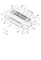
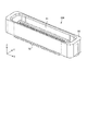
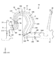
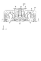
- FIG. 1 is a perspective view of the connector of the embodiment and other connectors after fitting.
- FIG. 2 is a plan view of the connector of the embodiment and other connectors after fitting.
- FIG. 3 is a cross-sectional view taken along the line AA of FIG.
- FIG. 4 is a cross-sectional view of the connector of the embodiment and other connectors before fitting.
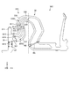
- FIG. 5 is a perspective view of an electronic device equipped with the connector of the embodiment.
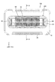
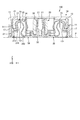
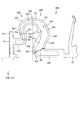
- FIG. 6 is a perspective view of the connector of the embodiment.
- FIG. 7 is a plan view of the connector of the embodiment.
- FIG. 8 is a bottom view of the connector of the embodiment.
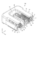
- FIG. 9 is an exploded perspective view of the connector of the embodiment.
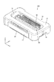
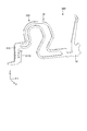
- FIG. 10 is a perspective view of another connector.
- FIG. 11 is a plan view of another connector.
- FIG. 12 is a cross-sectional view taken along the line BB of FIG.
- FIG. 13 is a perspective view of a cross section taken along the line BB of FIG.
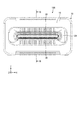
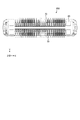
- FIG. 14 is a side view of the contacts of the embodiment.
- FIG. 15 is a schematic view of a connector of a comparative example.
- FIG. 16 is a graph showing the differential impedance of the connector of the embodiment and the connector of the comparative example.
- FIG. 17 is a side view of the contact of the first modification.
- FIG. 18 is a side view of the contact of the second modification.
- FIG. 19 is a side view of the contact of the third modification.
- FIG. 20 is a perspective view of the contact of the fourth modification.
- FIG. 21 is a cross-sectional view of the connector of the embodiment and the other connector of the fifth modification after fitting.
- FIG. 1 is a perspective view of the connector of the embodiment and other connectors after fitting.
- FIG. 2 is a plan view of the connector of the embodiment and other connectors after fitting.
- FIG. 3 is a cross-sectional view taken along the line AA of FIG.
- FIG. 4 is a cross-sectional view of the connector of the embodiment and other connectors before fitting.
- FIG. 5 is a perspective view of an electronic device equipped with the connector of the embodiment.
- FIG. 6 is a perspective view of the connector of the embodiment.
- FIG. 7 is a plan view of the connector of the embodiment.
- FIG. 8 is a bottom view of the connector of the embodiment.
- FIG. 9 is an exploded perspective view of the connector of the embodiment.
- FIG. 10 is a perspective view of another connector.
- FIG. 10 is a perspective view of another connector.
- FIG. 11 is a plan view of another connector.
- FIG. 12 is a cross-sectional view taken along the line BB of FIG.
- FIG. 13 is a perspective view of a cross section taken along the line BB of FIG.
- FIG. 14 is a side view of the contacts of the embodiment.
- the X-axis is an axis parallel to the direction in which the plurality of contacts 30 are lined up.
- the Z-axis is an axis parallel to the relative moving direction (fitting direction) when the connector 100 and the connector 200 are fitted.
- the Y-axis is an axis orthogonal to both the X-axis and the Z-axis.
- the XY plane is parallel to the substrate 300 and the substrate 400.
- the Z axis is orthogonal to the substrate 300 and the substrate 400.
- the direction along the X axis is described as the X direction
- the direction along the Y axis is described as the Y direction
- the direction along the Z axis is described as the Z direction.
- the direction from the substrate 300 to the substrate 400 is the + Z direction, and the direction opposite to the + Z direction is the ⁇ Z direction.
- the XY plan view means the case where it is viewed from the fitting direction.
- the YZ plan view means the case where it is viewed from the arrangement direction.
- the X direction is the direction in which a plurality of contacts 30 are lined up.
- the X direction is an arrangement direction in which a plurality of contacts 30 are arranged. It can be said that the X direction is the long side direction of the fixed insulator 10 in a plan view orthogonal to the substrate 300 and the substrate 400.
- the Y direction is a direction orthogonal to the substrate 300 and the substrate 400 and orthogonal to the direction in which the plurality of contacts 30 are lined up. It can be said that the Y direction is the short side direction of the fixed insulator 10 in a plan view orthogonal to the substrate 300 and the substrate 400.
- the Z direction is a relative moving direction (fitting direction) when the connector 100 and the connector 200 are fitted. It can be said that the Z direction is a direction orthogonal to the substrate 300 and the substrate 400.
- the connector 100 of the embodiment is attached to the substrate 300.
- the connector 100 is connected to another connector 200.
- the connector 200 is attached to the substrate 400.
- the board 300 and the board 400 are connected via the connector 100 and the connector 200.
- the substrate 300 and the substrate 400 are printed circuit boards (PCBs) and include a plurality of electronic components.
- the substrate 300 and the substrate 400 may be flexible substrates (Flexible Printed Circuits: FPC).
- the electronic device 1000 shown in FIG. 5 includes a connector 100 and a connector 200.
- the electronic device 1000 is an in-vehicle camera.
- the electronic device 1000 includes a lens unit 1001 including a lens and an electric wire unit 1002 including an electric wire.
- the connector 100 arranged on one of the lens portion 1001 and the electric wire portion 1002 is connected to the connector 200 arranged on the other side.
- the electronic device to which the connector 100 and the connector 200 are applied does not necessarily have to be an in-vehicle camera, and is not particularly limited.
- the connector 100 includes a fixed insulator 10, a fixture 40, a movable insulator 20, and a plurality of contacts 30.
- the connector 200 includes an insulator 60, a fixture 80, and a plurality of contacts 70.
- the contact 30 is fixed to the substrate 300 by soldering or the like.
- the plurality of contacts 30 are positioned by the fixed insulator 10 and the movable insulator 20.
- the plurality of contacts 30 are arranged along one direction (X direction).
- the contact 70 is fixed to the substrate 400 by soldering or the like.
- the plurality of contacts 70 are positioned by the insulator 60.
- the plurality of contacts 70 are arranged along one direction (X direction). When the contact 70 comes into contact with the contact 30, the substrate 300 and the substrate 400 are electrically connected.
- the insulator 60 is a member formed of an insulator.
- the insulator 60 is made of, for example, a synthetic resin.
- the insulator 60 includes a side wall 61 parallel to the XZ plane.
- the side wall 61 covers a part of the movable insulator 20 from both sides in the Y direction.
- the side wall 61 is arranged between the movable insulator 20 and the second arm portion 34 of the contact 30.
- the fixture 80 is a substantially L-shaped metal fitting.
- the fixture 80 is supported by the insulator 60.
- the fixture 80 is arranged inside the insulator 60.
- the fixture 80 is fixed to the substrate 400 by soldering or the like.
- the fixed insulator 10 is a frame-shaped member formed of an insulator.
- the fixed insulator 10 is formed of, for example, a synthetic resin.
- the fixture 40 is a substantially U-shaped metal fitting. The fixture 40 is supported by the fixed insulator 10. The fixture 40 is arranged inside the fixed insulator 10. The fixture 40 is fixed to the substrate 300 by soldering or the like.
- the fixed insulator 10 includes two first side walls 17, two second side walls 18, an upper wall 15, a plurality of first fixing grooves 11, and a plurality of partition walls 13. , Equipped with.
- the first side wall 17 is a wall parallel to the XZ plane.
- the two first side walls 17 are arranged with a gap in the Y direction.
- the second side wall 18 is a wall parallel to the YZ plane.
- the two second side walls 18 are arranged with a gap in the X direction.
- the second side wall 18 is connected to the ends of the two first side walls 17.
- the two first side walls 17 and the two second side walls 18 are arranged in a frame shape in an XY plan view.
- the upper wall 15 is a wall parallel to the XY plane.
- the upper wall 15 is arranged in the + Z direction of the first side wall 17 and the second side wall 18.
- the upper wall 15 covers at least a part of the contact 30.
- the upper wall 15 overlaps at least a part of the contact 30 in an XY plan view.
- the first fixing groove 11 is provided on the first side wall 17.
- the first fixing groove 11 extends along the Z direction.
- the longitudinal direction of the first fixing groove 11 is parallel to the Z direction.
- the plurality of first fixing grooves 11 are arranged at equal intervals along the X direction.
- the partition wall 13 is a wall parallel to the YZ plane.
- the partition wall 13 is connected to the first side wall 17 and the upper wall 15.
- the plurality of partition walls 13 are arranged at equal intervals along the X direction.
- the interval at which the plurality of partition walls 13 are arranged is equal to the interval at which the plurality of first fixing grooves 11 are arranged.
- the partition wall 13 is also called an interpolar wall.
- the partition wall 13 includes an inclined surface 131.
- the inclined surface 131 is inclined toward the virtual plane P so as to be separated from the second arm portion 34 of the contact 30 described later.
- the virtual plane P is a plane parallel to the XY plane and passing through the bottom surfaces of a plurality of first bases 31, which will be described later.
- the movable insulator 20 is formed of an insulator.
- the movable insulator 20 is made of, for example, a synthetic resin.
- the movable insulator 20 is arranged inside the fixed insulator 10.
- the movable insulator 20 is not fixed to the substrate 300.
- the movable insulator 20 is connected to the fixed insulator 10 via a contact 30.
- the movable insulator 20 can move with respect to the fixed insulator 10 due to the elastic deformation of the contact 30.
- the movable insulator 20 includes a second fixing groove 21.
- the second fixing groove 21 extends in the Z direction.
- the longitudinal direction of the second fixing groove 21 is parallel to the Z direction.
- the plurality of second fixing grooves 21 are arranged at equal intervals along the X direction.
- the contact 30 is a plate-shaped member made of metal.
- the thickness direction of the contacts 30 is parallel to the X direction (arrangement direction).
- the thickness (length in the X direction) of the contact 30 is constant.
- the surfaces of the contacts 30 facing the X direction are all flat surfaces parallel to the YZ plane.
- the thickness of the contact 30 (length in the X direction) is smaller than the minimum length of the contact 30 in the direction orthogonal to the X direction.
- the contact 30 is formed, for example, by punching a metal plate with a press machine.
- the contact 30 is a so-called fork type.
- the contact 30 includes a first base portion 31, a second base portion 32, a first arm portion 33, a second arm portion 34, and a contact portion 38.
- the first base portion 31 includes a convex portion 311 supported by the first fixing groove 11 of the fixed insulator 10.
- the convex portion 311 is press-fitted into the first fixing groove 11.
- the bottom surface of the first base 31 is connected to the substrate 300.
- the first base portion 31 includes a recess 313.
- the recess 313 is arranged at the connection portion of the first base portion 31 with the first arm portion 33.
- the second base portion 32 is supported by the second fixing groove 21 of the movable insulator 20.
- the second base portion 32 is press-fitted into the second fixing groove 21.
- the contact portion 38 comes into contact with the contact 70 of the connector 200.
- the first arm portion 33 is connected only to the first base portion 31 and the second arm portion 34. As shown in FIG. 13, the first arm portion 33 is arranged between two partition walls 13 adjacent to each other in the X direction. As shown in FIG. 14, the width of the first arm portion 33 is constant. The width is the length in the direction orthogonal to the center line C.
- the center line C is a line connecting points of the first arm portion 33 and the second arm portion 34 equidistant from two outer peripheral surfaces oriented in the direction orthogonal to the thickness direction (X direction). At the position where the center line C is a curve, the width is the length in the direction orthogonal to the tangent line of the center line C. It can be said that the width is the length in the direction orthogonal to the extending direction of the first arm portion 33 and the second arm portion 34.
- the first arm portion 33 includes a first slit 330, a first straight portion 331, a first bent portion 332, a second straight portion 333, a second bent portion 334, and a connecting portion. 335 and.
- the broken line in FIG. 14 indicates the position of the end portion of the partition wall 13 farthest from the first side wall 17 in the Y direction.
- the left side of the broken line in FIG. 14 is the space sandwiched between the partition walls 13.
- the right side of the broken line in FIG. 14 is the outside of the space sandwiched between the partition walls 13.
- the first slit 330 is a slit that penetrates the first arm portion 33 in the X direction.
- the number of the first slits 330 is one.
- the width of the first slit 330 is constant except for the end portion.
- the position of the center of the first slit 330 in the width direction is the same as the position of the center of the first arm 33 in the width direction. Therefore, the widths of the portions on both sides of the first slit 330 in the first arm portion 33 are constant except for the end portions and are equal to each other. That is, the width W3 of one portion of the first slit 330 in the first arm portion 33 is equal to the width W4 of the other portion of the first slit 330 in the first arm portion 33.
- the first straight line portion 331 is connected to the first base portion 31.
- the first straight line portion 331 is linear in a YZ plan view.
- the two outer peripheral surfaces of the first straight portion 331 facing in the direction orthogonal to the thickness direction are planar shapes parallel to each other.
- the first bent portion 332 is connected to the first straight portion 331.
- the first bent portion 332 is curved in a YZ plan view.
- the first bent portion 332 is bent in a YZ plan view.
- the two outer peripheral surfaces of the first bent portion 332 facing in the direction orthogonal to the thickness direction are curved surfaces.
- the first bent portion 332 is convex toward the second base portion 32.
- the second straight portion 333 is connected to the first bent portion 332.
- the second straight line portion 333 is linear in a YZ plan view.
- the two outer peripheral surfaces of the second straight portion 333 facing in the direction orthogonal to the thickness direction are planar shapes parallel to each other.
- the second bent portion 334 is connected to the second straight portion 333.
- the second bent portion 334 is curved in a YZ plan view.
- the second bent portion 334 is bent in a YZ plan view.
- the two outer peripheral surfaces of the second bent portion 334 facing in the direction orthogonal to the thickness direction are curved.
- the second bent portion 334 is convex toward the first base portion 31.
- the connecting portion 335 is connected to the second bent portion 334.
- the connecting portion 335 is linear in a YZ plan view.
- the two outer peripheral surfaces of the connecting portion 335 facing in the direction orthogonal to the thickness direction are planar shapes parallel to each other.
- the second arm portion 34 is connected only to the first arm portion 33 and the second base portion 32. As shown in FIG. 13, the second arm portion 34 is arranged closer to the second base portion 32 than the partition wall 13. The second arm portion 34 is arranged outside the space sandwiched between the two partition walls 13. As shown in FIG. 14, the width of the second arm portion 34 is not constant. The width of the second arm portion 34 is the minimum at the portion connected to the first arm portion 33.
- the second arm portion 34 includes a second slit 340, a connecting portion 341, a first straight portion 342, a first bent portion 343, a second straight portion 344, and a second bent portion.
- a 345 and a third straight line portion 346 are provided.
- the second slit 340 is a slit that penetrates the second arm portion 34 in the X direction.
- the number of the second slit 340 is one.
- the second slit 340 is connected to the first slit 330.
- the width of the second slit 340 is not constant.
- the position of the center in the width direction of the first slit 330 is the same as the position of the center in the width direction of the second arm portion 34.
- the widths of both sides of the second slit 340 in the second arm 34 are constant except for the ends and are equal to each other.
- the width W5 of one portion of the second slit 340 in the second arm portion 34 is equal to the width W6 of the other portion of the second slit 340 in the second arm portion 34.
- the widths 5 and W6 are equal to the widths W3 and 4 of the first arm 33.
- the connecting portion 341 is connected to the connecting portion 335 of the first arm portion 33.
- a part of the outer peripheral surface of the connecting portion 341 facing in the + Z direction is flat.
- the outer peripheral surface of the connecting portion 341 facing the + Z direction and the outer peripheral surface of the connecting portion 335 facing the + Z direction form a planar facing surface 35.
- the facing surface 35 faces the upper wall 15 of the fixed insulator 10.
- the first straight line portion 342 is connected to the connecting portion 341.
- the first straight line portion 342 is linear in a YZ plan view.
- the two outer peripheral surfaces of the first straight line portion 342 facing in the direction orthogonal to the thickness direction are planar shapes parallel to each other.
- the first bent portion 343 is connected to the first straight portion 342.
- the first bent portion 343 is curved in a YZ plan view.
- the first bent portion 343 is bent in a YZ plan view.
- the two outer peripheral surfaces of the first bent portion 343 facing in the direction orthogonal to the thickness direction are curved.
- the first bent portion 343 is convex toward the second base portion 32.
- the second straight portion 344 is connected to the first bent portion 343.
- the second straight line portion 344 is linear in the YZ plan view.
- the two outer peripheral surfaces of the second straight portion 344 facing in the direction orthogonal to the thickness direction are flat surfaces parallel to each other.
- the second bent portion 345 is connected to the second straight portion 344.
- the second bent portion 345 is curved in a YZ plan view.
- the second bent portion 345 is bent in a YZ plan view.
- the two outer peripheral surfaces of the second bent portion 345 facing in the direction orthogonal to the thickness direction are curved.
- the second bent portion 345 is convex toward the first base portion 31.
- the third straight line portion 346 is connected to the second bent portion 345 and the second base portion 32.
- the third straight line portion 346 is linear in a YZ plan view.
- the two outer peripheral surfaces of the third straight portion 346 facing in the direction orthogonal to the thickness direction are planar shapes parallel to each other.
- the third straight line portion 346 includes an inclined inner wall 3461.
- the inclined inner wall 3461 is an inner wall of the third straight line portion 346 facing the second slit 340.
- the inclined inner wall 3461 is inclined so that the width of the second slit 340 becomes smaller toward the second base portion 32.
- the width of the second arm portion 34 is the maximum at the second bent portion 345.
- the width of the second slit 340 is maximum at the second bent portion 345.
- the maximum width Wa of the first arm 33 is smaller than the maximum width Wb of the second arm 34.
- the maximum width W1 of the first slit 330 is smaller than the maximum width W2 of the second slit 340.
- FIG. 15 is a schematic view of a connector of a comparative example.
- FIG. 16 is a graph showing the differential impedance of the connector of the embodiment and the connector of the comparative example.
- the contact 30 is required to be capable of high-speed transmission. For that purpose, it is necessary to adjust the characteristic impedance of the contact 30 with higher accuracy. However, it is not easy to adjust the characteristic impedance of the contact 30 with higher accuracy.
- the contact of the comparative example has a shape different from that of the contact 30 of the present embodiment. In the comparative example, the maximum width of the portion corresponding to the first arm portion 33 is equal to the maximum width of the portion corresponding to the second arm portion 34.
- FIG. 16 shows the characteristic impedance of the contact 30 of the present embodiment and the characteristic impedance of the contact of the comparative example under the same experimental conditions.
- the change in the characteristic impedance of the contact of the comparative example is larger than the change in the characteristic impedance of the contact 30 of the present embodiment.
- the contact 30 of the present embodiment it is possible to reduce the change in the characteristic impedance of the contact 30.
- the characteristic impedance of the contact 30 tends to be too low in the portion (first arm portion 33) of the contact 30 that is arranged in the space sandwiched between the partition walls 13.
- the maximum width Wa of the first arm portion 33 is smaller than the maximum width Wb of the second arm portion 34. This prevents the characteristic impedance of the contact 30 from dropping too much.
- the shape of the contact 30 is not limited to the shape described above.
- the contact 30 may have a shape different from the above-described shape as long as the maximum width of the first arm portion 33 is smaller than the maximum width of the second arm portion 34. Further, the number of the first slit 330 and the number of the second slit 340 does not necessarily have to be one.
- the contact 30 may include a plurality of first slits 330 or a plurality of second slits 340.
- the convex portion 311 of the contact 30 does not have to be press-fitted into the first fixing groove 11 of the fixed insulator 10.
- the convex portion 311 and the first fixing groove 11 may be integrally formed by insert molding.
- the second base 32 of the contact 30 does not have to be press-fitted into the second fixing groove 21 of the movable insulator 20.
- the second base portion 32 and the second fixing groove 21 may be integrally molded by insert molding.
- the convex portion 311 and the first fixing groove 11 may be integrally formed by insert molding
- the second base portion 32 and the second fixing groove 21 may be integrally formed by insert molding.
- the connector 100 includes a fixed insulator 10, a movable insulator 20, and a plurality of contacts 30.
- the movable insulator 20 is arranged inside the fixed insulator 10 and is movable with respect to the fixed insulator 10.
- the contact 30 is attached to the fixed insulator 10 and the movable insulator 20.
- the fixed insulator 10 includes a plurality of first fixing grooves 11 arranged along an arrangement direction (X direction) in which a plurality of contacts 30 are arranged, and a partition wall 13 arranged between two adjacent contacts 30. ..
- the movable insulator 20 includes a plurality of second fixing grooves 21 arranged along the arrangement direction (X direction).
- the contact 30 is between the first base portion 31 supported by the first fixing groove 11, the second base portion 32 supported by the second fixing groove 21, and the two partition walls 13 connected to and adjacent to the first base portion 31.
- a first arm portion 33 arranged in the above, and a second arm portion 34 connected to the first arm portion 33 and the second base portion 32 are provided.
- the maximum width Wa of the first arm 33 is smaller than the maximum width Wb of the second arm 34.
- the contact 30 is easily elastically deformed because the maximum width Wa of the first arm 33 is smaller than the maximum width Wb of the second arm 34.
- the movable insulator 20 is easily moved. According to the connector 100, the flexibility at the time of floating can be improved. Further, since the maximum width W1 of the first slit 330 is smaller than the maximum width W2 of the second slit 340, it is suppressed that the characteristic impedance of the first arm portion 33 sandwiched between the partition walls 13 is excessively lowered. As a result, the characteristic impedance of the contact 30 can be adjusted with higher accuracy. Therefore, the connector 100 of the present embodiment can improve the flexibility and can adjust the characteristic impedance of the contact 30 with higher accuracy.
- the second arm portion 34 is arranged closer to the second base portion 32 than the partition wall 13. As a result, the movable area of the contact 30 is expanded.
- the thickness direction of the contacts 30 is the arrangement direction. Thereby, the contact 30 can be easily manufactured by punching the metal plate with a press machine.
- the connector 100 at least one of the first arm portion 33 and the second arm portion 34 has a straight straight portion (for example, the first straight portion 342) and a bent bent portion (for example, the first bent portion 343). Be prepared.
- the connector 100 of the present embodiment can stabilize the posture of the movable insulator 20 when moving.
- the contact 30 is easily elastically deformed.
- the connector 100 of the present embodiment can further improve the flexibility when floating.
- the first arm portion 33 includes a first slit 330 which is a slit penetrating in the arrangement direction (X direction).
- the second arm portion 34 includes a second slit 340 which is a slit penetrating in the arrangement direction (X direction).
- the maximum width W1 of the first slit 330 is smaller than the maximum width W2 of the second slit 340.
- the contact 30 is more likely to be elastically deformed.
- the connector 100 the flexibility at the time of floating can be further improved. Further, it is further suppressed that the characteristic impedance of the first arm portion 33 sandwiched between the partition walls 13 is lowered too much. Therefore, the connector 100 can adjust the characteristic impedance of the contact 30 with higher accuracy.
- the number of the first slit 330 and the number of the second slit 340 are one.
- the shape of the contact 30 is simplified and can be easily manufactured.
- the connector 100 of the present embodiment can adjust the characteristic impedance of the contact 30 with higher accuracy.
- width W3 and width W4 are equal to the widths of both sides of the second slit 340 in the second arm 34 (width W5 and width W6). ..
- the connector 100 of the present embodiment can adjust the characteristic impedance of the contact 30 with higher accuracy.
- the second arm portion 34 includes a first bent portion 343 that is convex toward the second base portion 32 and a second bent portion 345 that is convex toward the first base portion 31.
- the contact 30 is easily elastically deformed.
- the connector 100 of the present embodiment can further improve the flexibility when floating.
- the width of the second slit 340 is the maximum in the second bent portion 345.
- the contact 30 is easily elastically deformed.
- the connector 100 of the present embodiment can further improve the flexibility when floating.
- the second arm portion 34 has an inclined inner wall 3461 inclined between the second base portion 32 and the second bent portion 345 so that the width of the second slit 340 becomes smaller toward the second base portion 32. Be prepared. As a result, the rigidity of the inclined inner wall 3461 is improved, so that it is possible to prevent the inclined inner wall 3461 from being deformed when the contact 30 is press-fitted into the second fixing groove 21 of the movable insulator 20.
- the partition wall 13 includes an inclined surface 131 that is inclined so as to be separated from the second arm portion 34 toward the virtual plane P that passes through the bottom surfaces of the plurality of first base portions 31.
- FIG. 17 is a side view of the contact of the first modification.
- the contact 30A of the first modification includes a first arm portion 33A different from the first arm portion 33 described above.
- the same components as those described in the above-described embodiment are designated by the same reference numerals, and duplicate description will be omitted.
- the first arm portion 33A includes two first slits 330A and an intermediate portion 336.
- the first slit 330A is a slit that penetrates the first arm portion 33A in the X direction.
- One first slit 330A is provided from the first straight line portion 331 to the second straight line portion 333.
- Another first slit 330A is provided from the second straight line portion 333 to the connecting portion 335 and is connected to the second slit 340.
- the width of the first slit 330A is constant except for the end portion.
- the position of the center of the first slit 330A in the width direction is the same as the position of the center of the first arm 33A in the width direction.
- the widths of the portions on both sides of the first slit 330A in the first arm portion 33A are constant except for the end portions and are equal to each other.
- the maximum width W1 of the first slit 330A is smaller than the maximum width W2 of the second slit 340.
- the maximum width Wa of the first arm 33A is smaller than the maximum width Wb of the second arm 34.
- the intermediate portion 336 is arranged in the second straight portion 333.
- the intermediate portion 336 is provided between the two first slits 330A.
- the intermediate portion 336 does not necessarily have to be provided in the second straight portion 333.
- the intermediate portion 336 may be provided in the first straight portion 331, the first bent portion 332, the second bent portion 334, or the connecting portion 335.
- FIG. 18 is a side view of the contact of the second modification.
- the contact 30B of the second modification includes a first arm portion 33B different from the first arm portion 33 described above, and a second arm portion 34B different from the second arm portion 34. ..
- the same components as those described in the above-described embodiment are designated by the same reference numerals, and duplicate description will be omitted.
- the first arm portion 33B includes a convex portion 337.
- the convex portion 337 is provided on the outer peripheral surface of the second straight portion 333. Therefore, the width of the first arm portion 33B is not constant.
- the convex portion 337 may be provided on the inner peripheral surface of the second straight portion 333. Further, the convex portion 337 may be provided on the first straight portion 331, the first bent portion 332, the second bent portion 334, or the connecting portion 335.
- the second arm portion 34B includes a convex portion 347 and a convex portion 348.
- the convex portion 347 projects from the outer peripheral surface and the inner peripheral surface of the first straight portion 342.
- the convex portion 348 protrudes from the outer peripheral surface and the inner peripheral surface of the second straight portion 344. Therefore, the width of the second arm portion 34B is not constant.
- the convex portion 347 and the convex portion 348 may be provided on the connecting portion 341, the first bent portion 343, the second bent portion 345, or the third straight portion 346.
- the maximum width Wa of the first arm 33B is smaller than the maximum width Wb of the second arm 34B.
- FIG. 19 is a side view of the contact of the third modification.
- the contact 30C of the third modification includes a first arm portion 33C different from the first arm portion 33 described above.
- the same components as those described in the above-described embodiment are designated by the same reference numerals, and duplicate description will be omitted.
- the first arm portion 33C includes two first slits 330C and an intermediate portion 339.
- the first slit 330C is a slit that penetrates the first arm portion 33C in the X direction.
- the two first slits 330C are arranged so as to be adjacent to each other in the width direction.
- the two first slits 330C are provided from the first straight line portion 331 to the connecting portion 335.
- the width of the two first slits 330C is constant except for the ends.
- the center of the first slit 330C in the width direction is arranged on a line that divides the length of the first arm portion 33C in the width direction into three equal parts.
- the widths of the portions of the first arm portion 33C separated by the first slit 330C are constant except for the end portions and are equal to each other.
- the width W13, width W14 and width W15 shown in FIG. 19 are equal to each other.
- the maximum width W11 and the maximum width W12 of the first slit 330C are smaller than the maximum width W2 of the second slit 340.
- the maximum width Wa of the first arm 33C is smaller than the maximum width Wb of the second arm 34.
- the intermediate portion 339 is arranged at the connecting portion 335.
- the intermediate portion 336 is provided between the two first slits 330C and the second slit 340.
- the intermediate portion 339 does not necessarily have to be provided in the connecting portion 335.
- the intermediate portion 339 may be provided in the first straight portion 331, the first bent portion 332, the second straight portion 333, or the second bent portion 334.
- FIG. 20 is a perspective view of the contact of the fourth modification.
- the contact 30D of the fourth modification includes a first base portion 31D different from the first base portion 31 described above.
- the same components as those described in the above-described embodiment are designated by the same reference numerals, and duplicate description will be omitted.
- the first base portion 31D includes a convex portion 311D that fits into the first fixing groove 11 of the fixed insulator 10.
- the convex portion 311D is press-fitted into the first fixing groove 11.
- the convex portion 311D is formed by bending a part of the first base portion 31 in the arrangement direction (X direction) in which a plurality of contacts 30 are lined up.
- FIG. 21 is a cross-sectional view of the connector of the embodiment and the other connector of the fifth modification after fitting.
- the same components as those described in the above-described embodiment are designated by the same reference numerals, and duplicate description will be omitted.
- the other connector 200E of the fifth modification includes an insulator 60E.
- the insulator 60E is a member formed of an insulator.
- the insulator 60E is made of, for example, a synthetic resin.
- the insulator 60E does not include the side wall 61 described above. Since the space between the fixed insulator 10 and the movable insulator 20 is widened, it is possible to prevent the contact 30 from coming into contact with the side wall 61 when the contact 30 is elastically deformed. Further, by not providing the side wall 61, the connector of the embodiment can be miniaturized in the direction orthogonal to the arrangement direction (Y direction).
- the partition wall 13 may extend to the virtual plane Q as shown in FIG.
- the virtual plane Q is a plane that is parallel to the XY plane and passes through the bottom surface of the fixed insulator 10.
Landscapes
- Details Of Connecting Devices For Male And Female Coupling (AREA)
- Coupling Device And Connection With Printed Circuit (AREA)
Abstract
Description
図1は、実施形態のコネクタ及び他のコネクタの嵌合後の斜視図である。図2は、実施形態のコネクタ及び他のコネクタの嵌合後の平面図である。図3は、図2のA-A断面図である。図4は、実施形態のコネクタ及び他のコネクタの嵌合前の断面図である。図5は、実施形態のコネクタを搭載する電子機器の斜視図である。図6は、実施形態のコネクタの斜視図である。図7は、実施形態のコネクタの平面図である。図8は、実施形態のコネクタの底面図である。図9は、実施形態のコネクタの分解斜視図である。図10は、他のコネクタの斜視図である。図11は、他のコネクタの平面図である。図12は、図7のB-B断面図である。図13は、図7のB-B断面の斜視図である。図14は、実施形態のコンタクトの側面図である。
図17は、第1変形例のコンタクトの側面図である。図17に示すように、第1変形例のコンタクト30Aは、上述した第1腕部33とは異なる第1腕部33Aを備える。なお、上述した実施形態で説明したものと同じ構成要素には同一の符号を付して重複する説明は省略する。
図18は、第2変形例のコンタクトの側面図である。図18に示すように、第2変形例のコンタクト30Bは、上述した第1腕部33とは異なる第1腕部33Bと、第2腕部34とは異なる第2腕部34Bと、を備える。なお、上述した実施形態で説明したものと同じ構成要素には同一の符号を付して重複する説明は省略する。
図19は、第3変形例のコンタクトの側面図である。図19に示すように、第3変形例のコンタクト30Cは、上述した第1腕部33とは異なる第1腕部33Cを備える。なお、上述した実施形態で説明したものと同じ構成要素には同一の符号を付して重複する説明は省略する。
図20は、第4変形例のコンタクトの斜視図である。図20に示すように、第4変形例のコンタクト30Dは、上述した第1基部31とは異なる第1基部31Dを備える。なお、上述した実施形態で説明したものと同じ構成要素には同一の符号を付して重複する説明は省略する。
図21は、実施形態のコネクタ及び第5変形例の他のコネクタの嵌合後の断面図である。なお、上述した実施形態で説明したものと同じ構成要素には同一の符号を付して重複する説明は省略する。
11 第1固定溝
13 隔壁
15 上壁
17 第1側壁
18 第2側壁
20 可動インシュレータ
21 第2固定溝
30、30A、30B、30C、30D コンタクト
31、31D 第1基部
32 第2基部
33、33A、33B、33C、33D 第1腕部
34、34B 第2腕部
35 対向面
38 接触部
40 固定具
60、60E インシュレータ
61 側壁
70 コンタクト
80 固定具
100 コネクタ
131 傾斜面
200、200E コネクタ
300 基板
311、311D 凸部
313 凹部
330、330A、330C 第1スリット
331 第1直線部
332 第1屈曲部
333 第2直線部
334 第2屈曲部
335 接続部
336 中間部
337 凸部
339 中間部
340 第2スリット
341 接続部
342 第1直線部
343 第1屈曲部
344 第2直線部
345 第2屈曲部
346 第3直線部
347、348 凸部
400 基板
1000 電子機器
3461 傾斜内壁
C 中心線
P 仮想平面
Claims (12)
- 固定インシュレータと、
前記固定インシュレータの内側に配置され且つ前記固定インシュレータに対して移動可能な可動インシュレータと、
前記固定インシュレータ及び前記可動インシュレータに取り付けられる複数のコンタクトと、
を備え、
前記固定インシュレータは、複数の前記コンタクトが並ぶ配列方向に沿って配置される複数の第1固定溝と、隣接する2つの前記コンタクトの間に配置される隔壁と、を備え、
前記可動インシュレータは、前記配列方向に沿って配置される複数の第2固定溝を備え、
前記コンタクトは、前記第1固定溝に支持される第1基部と、前記第2固定溝に支持される第2基部と、前記第1基部と接続され且つ隣接する2つの前記隔壁の間に配置される第1腕部と、前記第1腕部及び前記第2基部に接続される第2腕部と、を備え、
前記第1腕部の最大幅は、前記第2腕部の最大幅よりも小さい
コネクタ。 - 前記第2腕部は、前記隔壁よりも前記第2基部側に配置される
請求項1に記載のコネクタ。 - 前記コンタクトの厚み方向は、前記配列方向である
請求項1又は2に記載のコネクタ。 - 前記第1腕部及び前記第2腕部の少なくとも一方は、直線状の直線部と、屈曲した屈曲部と、を備える
請求項1から3のいずれか1項に記載のコネクタ。 - 前記第1腕部は、前記配列方向に貫通するスリットである第1スリットを備え、
前記第2腕部は、前記配列方向に貫通するスリットである第2スリットを備え、
前記第1スリットの最大幅は、前記第2スリットの最大幅よりも小さい
請求項1から4のいずれか1項に記載のコネクタ。 - 前記第1スリットの数及び前記第2スリットの数は、1つである
請求項5に記載のコネクタ。 - 前記第1腕部における第1スリットの両側の部分の幅は、前記第2腕部における第2スリットの両側の部分の幅と等しい
請求項6に記載のコネクタ。 - 前記第2腕部は、前記第2基部に向かって凸である第1屈曲部と、前記第1基部に向かって凸である第2屈曲部と、を備える
請求項6又は7に記載のコネクタ。 - 前記第2スリットの幅は、前記第2屈曲部において最大となる
請求項8に記載のコネクタ。 - 前記第2腕部は、前記第2基部と前記第2屈曲部との間に、前記第2基部に向かって前記第2スリットの幅が小さくなるように傾斜する傾斜内壁を備える
請求項8又は9に記載のコネクタ。 - 前記隔壁は、複数の前記第1基部の底面を通過する仮想平面に向かって前記第2腕部から離れるように傾斜する傾斜面を備える
請求項1から10のいずれか1項に記載のコネクタ。 - 請求項1から11のいずれか1項に記載のコネクタを備える電子機器。
Priority Applications (4)
| Application Number | Priority Date | Filing Date | Title |
|---|---|---|---|
| EP20847265.4A EP4007077B1 (en) | 2019-07-26 | 2020-07-16 | Connector and electronic device |
| CN202080047483.4A CN114041245B (zh) | 2019-07-26 | 2020-07-16 | 连接器和电子设备 |
| KR1020227002598A KR102830833B1 (ko) | 2019-07-26 | 2020-07-16 | 커넥터 및 전자기기 |
| US17/618,822 US12003049B2 (en) | 2019-07-26 | 2020-07-16 | Connector and electronic device |
Applications Claiming Priority (2)
| Application Number | Priority Date | Filing Date | Title |
|---|---|---|---|
| JP2019138318A JP6687790B1 (ja) | 2019-07-26 | 2019-07-26 | コネクタ及び電子機器 |
| JP2019-138318 | 2019-07-26 |
Publications (1)
| Publication Number | Publication Date |
|---|---|
| WO2021020152A1 true WO2021020152A1 (ja) | 2021-02-04 |
Family
ID=70413758
Family Applications (1)
| Application Number | Title | Priority Date | Filing Date |
|---|---|---|---|
| PCT/JP2020/027734 Ceased WO2021020152A1 (ja) | 2019-07-26 | 2020-07-16 | コネクタ及び電子機器 |
Country Status (6)
| Country | Link |
|---|---|
| US (1) | US12003049B2 (ja) |
| EP (1) | EP4007077B1 (ja) |
| JP (1) | JP6687790B1 (ja) |
| KR (1) | KR102830833B1 (ja) |
| CN (1) | CN114041245B (ja) |
| WO (1) | WO2021020152A1 (ja) |
Cited By (1)
| Publication number | Priority date | Publication date | Assignee | Title |
|---|---|---|---|---|
| WO2023243471A1 (ja) * | 2022-06-15 | 2023-12-21 | 京セラ株式会社 | コネクタ及び電子機器 |
Families Citing this family (6)
| Publication number | Priority date | Publication date | Assignee | Title |
|---|---|---|---|---|
| JP6687790B1 (ja) * | 2019-07-26 | 2020-04-28 | 京セラ株式会社 | コネクタ及び電子機器 |
| CN113346285B (zh) | 2021-05-31 | 2023-04-11 | 上海航天科工电器研究院有限公司 | 电连接器及车载电子装置 |
| CN113488789B (zh) | 2021-05-31 | 2022-09-09 | 上海航天科工电器研究院有限公司 | 导体结构及电连接模块 |
| US12456831B2 (en) * | 2021-10-12 | 2025-10-28 | Xerox Corporation | Multi-part sensing electrode connector |
| CN116387878B (zh) * | 2023-05-18 | 2025-09-12 | 上海航天科工电器研究院有限公司 | 浮动端子组件、母连接器及浮动连接装置 |
| CN116454661B (zh) * | 2023-05-18 | 2026-01-09 | 上海航天科工电器研究院有限公司 | 稳定型导电端子、连接器及浮动连接器组件 |
Citations (4)
| Publication number | Priority date | Publication date | Assignee | Title |
|---|---|---|---|---|
| JP2012129109A (ja) | 2010-12-16 | 2012-07-05 | Japan Aviation Electronics Industry Ltd | コネクタ及びそれに用いるコンタクト |
| JP2015035352A (ja) * | 2013-08-09 | 2015-02-19 | ヒロセ電機株式会社 | コネクタ |
| JP2015176861A (ja) * | 2014-03-18 | 2015-10-05 | 日本航空電子工業株式会社 | コネクタ |
| JP2018160472A (ja) * | 2016-08-10 | 2018-10-11 | 京セラ株式会社 | コネクタ |
Family Cites Families (38)
| Publication number | Priority date | Publication date | Assignee | Title |
|---|---|---|---|---|
| JP2008084756A (ja) * | 2006-09-28 | 2008-04-10 | I-Pex Co Ltd | コネクタ装置 |
| JP5590991B2 (ja) * | 2010-06-30 | 2014-09-17 | 京セラコネクタプロダクツ株式会社 | コネクタ |
| JP5499191B1 (ja) * | 2013-01-28 | 2014-05-21 | 日本航空電子工業株式会社 | コネクタ |
| JP6116056B2 (ja) * | 2013-08-07 | 2017-04-19 | 日本航空電子工業株式会社 | コネクタ |
| JP5481594B1 (ja) * | 2013-08-09 | 2014-04-23 | イリソ電子工業株式会社 | コネクタ端子及び電気コネクタ |
| KR101514919B1 (ko) * | 2014-02-25 | 2015-04-23 | 엘에스엠트론 주식회사 | 전기 커넥터의 플러그와 리셉터클 및 이를 포함하는 전기 커넥터 어셈블리 |
| JP5748378B2 (ja) | 2014-08-04 | 2015-07-15 | 日本航空電子工業株式会社 | コネクタ及びそれに用いるコンタクト |
| JP5849166B1 (ja) * | 2014-12-12 | 2016-01-27 | イリソ電子工業株式会社 | 基板間接続構造 |
| JP6662633B2 (ja) * | 2015-12-28 | 2020-03-11 | 京セラ株式会社 | フローティングコネクタ装置 |
| JP6806529B2 (ja) * | 2016-11-02 | 2021-01-06 | 日本航空電子工業株式会社 | フローティングコネクタ及び電気コネクタ |
| JP6446109B1 (ja) * | 2017-10-10 | 2018-12-26 | イリソ電子工業株式会社 | コネクタ |
| JP6408106B1 (ja) * | 2017-10-25 | 2018-10-17 | 京セラ株式会社 | コネクタ及び電子機器 |
| US10199761B1 (en) * | 2017-11-22 | 2019-02-05 | Greenconn Corp. | Signal transmission assembly and floating connector |
| JP6582082B2 (ja) * | 2018-03-09 | 2019-09-25 | 京セラ株式会社 | コネクタ及び電子機器 |
| JP2019192527A (ja) * | 2018-04-26 | 2019-10-31 | ヒロセ電機株式会社 | 回路基板用電気コネクタ |
| US10320124B1 (en) * | 2018-05-02 | 2019-06-11 | All Best Precision Technology Co., Ltd. | Electrical connector with internal terminals having opposite sides located from connector internal sidewalls |
| JP7109303B2 (ja) * | 2018-08-07 | 2022-07-29 | 日本航空電子工業株式会社 | コネクタ組立体 |
| JP7093273B2 (ja) * | 2018-09-07 | 2022-06-29 | 日本航空電子工業株式会社 | コネクタ |
| TWI712227B (zh) * | 2018-09-11 | 2020-12-01 | 禾昌興業股份有限公司 | 浮動連接器及連接機構總成 |
| JP7002432B2 (ja) * | 2018-10-23 | 2022-01-20 | 京セラ株式会社 | コネクタ及びコネクタの製造方法 |
| JP7207975B2 (ja) * | 2018-11-29 | 2023-01-18 | イリソ電子工業株式会社 | コネクタ |
| WO2020209027A1 (ja) * | 2019-04-10 | 2020-10-15 | パナソニックIpマネジメント株式会社 | コネクタ、接続装置及び接続方法 |
| JP6687790B1 (ja) * | 2019-07-26 | 2020-04-28 | 京セラ株式会社 | コネクタ及び電子機器 |
| EP4007076B1 (en) * | 2019-07-29 | 2025-12-10 | Iriso Electronics Co., Ltd. | Connector |
| JP7297622B2 (ja) * | 2019-09-20 | 2023-06-26 | 日本航空電子工業株式会社 | フローティングコネクタ |
| JP7161463B2 (ja) * | 2019-10-10 | 2022-10-26 | ヒロセ電機株式会社 | 電気コネクタ及びその製造方法 |
| JP7393980B2 (ja) * | 2020-03-05 | 2023-12-07 | ヒロセ電機株式会社 | 回路基板用電気コネクタおよび回路基板付電気コネクタ |
| JP7467236B2 (ja) * | 2020-05-28 | 2024-04-15 | 日本航空電子工業株式会社 | フローティングコネクタ |
| JP7467234B2 (ja) * | 2020-05-28 | 2024-04-15 | 日本航空電子工業株式会社 | フローティングコネクタ |
| JP7411505B2 (ja) * | 2020-06-03 | 2024-01-11 | ホシデン株式会社 | シールド部材、シールドユニット、及びコネクタモジュール |
| JP7557983B2 (ja) * | 2020-07-15 | 2024-09-30 | 日本航空電子工業株式会社 | フローティングコネクタ |
| JP7667703B2 (ja) * | 2021-07-07 | 2025-04-23 | モレックス エルエルシー | コネクタ |
| TWI836299B (zh) * | 2021-12-02 | 2024-03-21 | 禾昌興業股份有限公司 | 浮動式多端子連接器 |
| JP7732917B2 (ja) * | 2022-02-03 | 2025-09-02 | ヒロセ電機株式会社 | 回路基板用電気コネクタ |
| EP4250493B1 (en) * | 2022-03-22 | 2025-03-05 | Japan Aviation Electronics Industry, Limited | Floating connector |
| JP2023141246A (ja) * | 2022-03-23 | 2023-10-05 | イリソ電子工業株式会社 | コネクタセット及び第一コネクタ |
| CN114784533A (zh) * | 2022-04-08 | 2022-07-22 | 厦门广泓工贸有限公司 | 一种电连接件和浮动式连接器 |
| TWM656855U (zh) * | 2022-06-01 | 2024-06-21 | 大陸商安費諾商用電子產品(成都)有限公司 | 電連接器及相關電子總成 |
-
2019
- 2019-07-26 JP JP2019138318A patent/JP6687790B1/ja active Active
-
2020
- 2020-07-16 KR KR1020227002598A patent/KR102830833B1/ko active Active
- 2020-07-16 EP EP20847265.4A patent/EP4007077B1/en active Active
- 2020-07-16 WO PCT/JP2020/027734 patent/WO2021020152A1/ja not_active Ceased
- 2020-07-16 CN CN202080047483.4A patent/CN114041245B/zh active Active
- 2020-07-16 US US17/618,822 patent/US12003049B2/en active Active
Patent Citations (4)
| Publication number | Priority date | Publication date | Assignee | Title |
|---|---|---|---|---|
| JP2012129109A (ja) | 2010-12-16 | 2012-07-05 | Japan Aviation Electronics Industry Ltd | コネクタ及びそれに用いるコンタクト |
| JP2015035352A (ja) * | 2013-08-09 | 2015-02-19 | ヒロセ電機株式会社 | コネクタ |
| JP2015176861A (ja) * | 2014-03-18 | 2015-10-05 | 日本航空電子工業株式会社 | コネクタ |
| JP2018160472A (ja) * | 2016-08-10 | 2018-10-11 | 京セラ株式会社 | コネクタ |
Non-Patent Citations (1)
| Title |
|---|
| See also references of EP4007077A4 |
Cited By (3)
| Publication number | Priority date | Publication date | Assignee | Title |
|---|---|---|---|---|
| WO2023243471A1 (ja) * | 2022-06-15 | 2023-12-21 | 京セラ株式会社 | コネクタ及び電子機器 |
| JPWO2023243471A1 (ja) * | 2022-06-15 | 2023-12-21 | ||
| JP7820514B2 (ja) | 2022-06-15 | 2026-02-25 | 京セラ株式会社 | コネクタ及び電子機器 |
Also Published As
| Publication number | Publication date |
|---|---|
| EP4007077A1 (en) | 2022-06-01 |
| JP6687790B1 (ja) | 2020-04-28 |
| KR20220024967A (ko) | 2022-03-03 |
| US20220239026A1 (en) | 2022-07-28 |
| KR102830833B1 (ko) | 2025-07-08 |
| CN114041245B (zh) | 2024-11-26 |
| CN114041245A (zh) | 2022-02-11 |
| JP2021022488A (ja) | 2021-02-18 |
| EP4007077A4 (en) | 2023-08-16 |
| EP4007077B1 (en) | 2026-01-28 |
| US12003049B2 (en) | 2024-06-04 |
Similar Documents
| Publication | Publication Date | Title |
|---|---|---|
| JP6687790B1 (ja) | コネクタ及び電子機器 | |
| US10916875B2 (en) | Connector and connector assembly | |
| US10651581B1 (en) | Connector | |
| US11158968B2 (en) | Connector and connector assembly | |
| JP7388901B2 (ja) | コネクタ | |
| US11552421B2 (en) | Electrical connector with floating contacts each with multiple impedances | |
| US7795540B2 (en) | Extendable cable or extendable connecting member | |
| US11381019B2 (en) | Connector and electronic device | |
| US11349240B2 (en) | Floating connector and electronic device | |
| US10834834B2 (en) | Electrical connection box | |
| JP5748378B2 (ja) | コネクタ及びそれに用いるコンタクト | |
| JP2012129109A (ja) | コネクタ及びそれに用いるコンタクト | |
| US11322870B2 (en) | Connector and electronic device | |
| JP7002432B2 (ja) | コネクタ及びコネクタの製造方法 | |
| CN115136419B (zh) | 连接器及连接器组 | |
| CN114830453B (zh) | 连接器及电子设备 | |
| EP3595417A1 (en) | Control unit having press-fit structure | |
| CN112803180B (zh) | 逆变器装置 | |
| WO2009093415A1 (ja) | 実装構造体 | |
| CN114424408B (zh) | 电子器件及电子设备 | |
| JP6002636B2 (ja) | フラットケーブル端末接続具 | |
| JP4820248B2 (ja) | 電装基板、および画像形成装置 | |
| JP2007242561A (ja) | コネクタ構造体 | |
| KR102185663B1 (ko) | 케이블 커넥터 | |
| WO2022153819A1 (ja) | 多層電子基板 |
Legal Events
| Date | Code | Title | Description |
|---|---|---|---|
| 121 | Ep: the epo has been informed by wipo that ep was designated in this application |
Ref document number: 20847265 Country of ref document: EP Kind code of ref document: A1 |
|
| ENP | Entry into the national phase |
Ref document number: 20227002598 Country of ref document: KR Kind code of ref document: A |
|
| NENP | Non-entry into the national phase |
Ref country code: DE |
|
| ENP | Entry into the national phase |
Ref document number: 2020847265 Country of ref document: EP Effective date: 20220228 |
|
| WWG | Wipo information: grant in national office |
Ref document number: 2020847265 Country of ref document: EP |