WO2021024719A1 - 垂直共振器型発光素子 - Google Patents
垂直共振器型発光素子 Download PDFInfo
- Publication number
- WO2021024719A1 WO2021024719A1 PCT/JP2020/027475 JP2020027475W WO2021024719A1 WO 2021024719 A1 WO2021024719 A1 WO 2021024719A1 JP 2020027475 W JP2020027475 W JP 2020027475W WO 2021024719 A1 WO2021024719 A1 WO 2021024719A1
- Authority
- WO
- WIPO (PCT)
- Prior art keywords
- electrode
- light emitting
- layer
- semiconductor substrate
- multilayer film
- Prior art date
- Legal status (The legal status is an assumption and is not a legal conclusion. Google has not performed a legal analysis and makes no representation as to the accuracy of the status listed.)
- Ceased
Links
Images








Classifications
-
- H—ELECTRICITY
- H01—ELECTRIC ELEMENTS
- H01S—DEVICES USING THE PROCESS OF LIGHT AMPLIFICATION BY STIMULATED EMISSION OF RADIATION [LASER] TO AMPLIFY OR GENERATE LIGHT; DEVICES USING STIMULATED EMISSION OF ELECTROMAGNETIC RADIATION IN WAVE RANGES OTHER THAN OPTICAL
- H01S5/00—Semiconductor lasers
- H01S5/04—Processes or apparatus for excitation, e.g. pumping, e.g. by electron beams
- H01S5/042—Electrical excitation ; Circuits therefor
- H01S5/0425—Electrodes, e.g. characterised by the structure
- H01S5/04254—Electrodes, e.g. characterised by the structure characterised by the shape
-
- H—ELECTRICITY
- H01—ELECTRIC ELEMENTS
- H01S—DEVICES USING THE PROCESS OF LIGHT AMPLIFICATION BY STIMULATED EMISSION OF RADIATION [LASER] TO AMPLIFY OR GENERATE LIGHT; DEVICES USING STIMULATED EMISSION OF ELECTROMAGNETIC RADIATION IN WAVE RANGES OTHER THAN OPTICAL
- H01S5/00—Semiconductor lasers
- H01S5/10—Construction or shape of the optical resonator, e.g. extended or external cavity, coupled cavities, bent-guide, varying width, thickness or composition of the active region
- H01S5/18—Surface-emitting [SE] lasers, e.g. having both horizontal and vertical cavities
- H01S5/183—Surface-emitting [SE] lasers, e.g. having both horizontal and vertical cavities having only vertical cavities, e.g. vertical cavity surface-emitting lasers [VCSEL]
- H01S5/18361—Structure of the reflectors, e.g. hybrid mirrors
- H01S5/18369—Structure of the reflectors, e.g. hybrid mirrors based on dielectric materials
-
- H—ELECTRICITY
- H01—ELECTRIC ELEMENTS
- H01S—DEVICES USING THE PROCESS OF LIGHT AMPLIFICATION BY STIMULATED EMISSION OF RADIATION [LASER] TO AMPLIFY OR GENERATE LIGHT; DEVICES USING STIMULATED EMISSION OF ELECTROMAGNETIC RADIATION IN WAVE RANGES OTHER THAN OPTICAL
- H01S5/00—Semiconductor lasers
- H01S5/005—Optical components external to the laser cavity, specially adapted therefor, e.g. for homogenisation or merging of the beams or for manipulating laser pulses, e.g. pulse shaping
- H01S5/0064—Anti-reflection components, e.g. optical isolators
-
- H—ELECTRICITY
- H01—ELECTRIC ELEMENTS
- H01S—DEVICES USING THE PROCESS OF LIGHT AMPLIFICATION BY STIMULATED EMISSION OF RADIATION [LASER] TO AMPLIFY OR GENERATE LIGHT; DEVICES USING STIMULATED EMISSION OF ELECTROMAGNETIC RADIATION IN WAVE RANGES OTHER THAN OPTICAL
- H01S5/00—Semiconductor lasers
- H01S5/04—Processes or apparatus for excitation, e.g. pumping, e.g. by electron beams
- H01S5/042—Electrical excitation ; Circuits therefor
- H01S5/0425—Electrodes, e.g. characterised by the structure
- H01S5/04252—Electrodes, e.g. characterised by the structure characterised by the material
-
- H—ELECTRICITY
- H01—ELECTRIC ELEMENTS
- H01S—DEVICES USING THE PROCESS OF LIGHT AMPLIFICATION BY STIMULATED EMISSION OF RADIATION [LASER] TO AMPLIFY OR GENERATE LIGHT; DEVICES USING STIMULATED EMISSION OF ELECTROMAGNETIC RADIATION IN WAVE RANGES OTHER THAN OPTICAL
- H01S5/00—Semiconductor lasers
- H01S5/04—Processes or apparatus for excitation, e.g. pumping, e.g. by electron beams
- H01S5/042—Electrical excitation ; Circuits therefor
- H01S5/0425—Electrodes, e.g. characterised by the structure
- H01S5/04252—Electrodes, e.g. characterised by the structure characterised by the material
- H01S5/04253—Electrodes, e.g. characterised by the structure characterised by the material having specific optical properties, e.g. transparent electrodes
-
- H—ELECTRICITY
- H01—ELECTRIC ELEMENTS
- H01S—DEVICES USING THE PROCESS OF LIGHT AMPLIFICATION BY STIMULATED EMISSION OF RADIATION [LASER] TO AMPLIFY OR GENERATE LIGHT; DEVICES USING STIMULATED EMISSION OF ELECTROMAGNETIC RADIATION IN WAVE RANGES OTHER THAN OPTICAL
- H01S5/00—Semiconductor lasers
- H01S5/04—Processes or apparatus for excitation, e.g. pumping, e.g. by electron beams
- H01S5/042—Electrical excitation ; Circuits therefor
- H01S5/0425—Electrodes, e.g. characterised by the structure
- H01S5/04256—Electrodes, e.g. characterised by the structure characterised by the configuration
-
- H—ELECTRICITY
- H01—ELECTRIC ELEMENTS
- H01S—DEVICES USING THE PROCESS OF LIGHT AMPLIFICATION BY STIMULATED EMISSION OF RADIATION [LASER] TO AMPLIFY OR GENERATE LIGHT; DEVICES USING STIMULATED EMISSION OF ELECTROMAGNETIC RADIATION IN WAVE RANGES OTHER THAN OPTICAL
- H01S5/00—Semiconductor lasers
- H01S5/10—Construction or shape of the optical resonator, e.g. extended or external cavity, coupled cavities, bent-guide, varying width, thickness or composition of the active region
- H01S5/18—Surface-emitting [SE] lasers, e.g. having both horizontal and vertical cavities
- H01S5/183—Surface-emitting [SE] lasers, e.g. having both horizontal and vertical cavities having only vertical cavities, e.g. vertical cavity surface-emitting lasers [VCSEL]
- H01S5/18305—Surface-emitting [SE] lasers, e.g. having both horizontal and vertical cavities having only vertical cavities, e.g. vertical cavity surface-emitting lasers [VCSEL] with emission through the substrate, i.e. bottom emission
-
- H—ELECTRICITY
- H01—ELECTRIC ELEMENTS
- H01S—DEVICES USING THE PROCESS OF LIGHT AMPLIFICATION BY STIMULATED EMISSION OF RADIATION [LASER] TO AMPLIFY OR GENERATE LIGHT; DEVICES USING STIMULATED EMISSION OF ELECTROMAGNETIC RADIATION IN WAVE RANGES OTHER THAN OPTICAL
- H01S5/00—Semiconductor lasers
- H01S5/10—Construction or shape of the optical resonator, e.g. extended or external cavity, coupled cavities, bent-guide, varying width, thickness or composition of the active region
- H01S5/18—Surface-emitting [SE] lasers, e.g. having both horizontal and vertical cavities
- H01S5/183—Surface-emitting [SE] lasers, e.g. having both horizontal and vertical cavities having only vertical cavities, e.g. vertical cavity surface-emitting lasers [VCSEL]
- H01S5/18308—Surface-emitting [SE] lasers, e.g. having both horizontal and vertical cavities having only vertical cavities, e.g. vertical cavity surface-emitting lasers [VCSEL] having a special structure for lateral current or light confinement
- H01S5/18322—Position of the structure
- H01S5/18327—Structure being part of a DBR
-
- H—ELECTRICITY
- H01—ELECTRIC ELEMENTS
- H01S—DEVICES USING THE PROCESS OF LIGHT AMPLIFICATION BY STIMULATED EMISSION OF RADIATION [LASER] TO AMPLIFY OR GENERATE LIGHT; DEVICES USING STIMULATED EMISSION OF ELECTROMAGNETIC RADIATION IN WAVE RANGES OTHER THAN OPTICAL
- H01S5/00—Semiconductor lasers
- H01S5/10—Construction or shape of the optical resonator, e.g. extended or external cavity, coupled cavities, bent-guide, varying width, thickness or composition of the active region
- H01S5/18—Surface-emitting [SE] lasers, e.g. having both horizontal and vertical cavities
- H01S5/183—Surface-emitting [SE] lasers, e.g. having both horizontal and vertical cavities having only vertical cavities, e.g. vertical cavity surface-emitting lasers [VCSEL]
- H01S5/18308—Surface-emitting [SE] lasers, e.g. having both horizontal and vertical cavities having only vertical cavities, e.g. vertical cavity surface-emitting lasers [VCSEL] having a special structure for lateral current or light confinement
- H01S5/18322—Position of the structure
- H01S5/1833—Position of the structure with more than one structure
-
- H—ELECTRICITY
- H01—ELECTRIC ELEMENTS
- H01S—DEVICES USING THE PROCESS OF LIGHT AMPLIFICATION BY STIMULATED EMISSION OF RADIATION [LASER] TO AMPLIFY OR GENERATE LIGHT; DEVICES USING STIMULATED EMISSION OF ELECTROMAGNETIC RADIATION IN WAVE RANGES OTHER THAN OPTICAL
- H01S5/00—Semiconductor lasers
- H01S5/10—Construction or shape of the optical resonator, e.g. extended or external cavity, coupled cavities, bent-guide, varying width, thickness or composition of the active region
- H01S5/18—Surface-emitting [SE] lasers, e.g. having both horizontal and vertical cavities
- H01S5/183—Surface-emitting [SE] lasers, e.g. having both horizontal and vertical cavities having only vertical cavities, e.g. vertical cavity surface-emitting lasers [VCSEL]
- H01S5/18361—Structure of the reflectors, e.g. hybrid mirrors
-
- H—ELECTRICITY
- H01—ELECTRIC ELEMENTS
- H01S—DEVICES USING THE PROCESS OF LIGHT AMPLIFICATION BY STIMULATED EMISSION OF RADIATION [LASER] TO AMPLIFY OR GENERATE LIGHT; DEVICES USING STIMULATED EMISSION OF ELECTROMAGNETIC RADIATION IN WAVE RANGES OTHER THAN OPTICAL
- H01S5/00—Semiconductor lasers
- H01S5/02—Structural details or components not essential to laser action
- H01S5/0206—Substrates, e.g. growth, shape, material, removal or bonding
- H01S5/0217—Removal of the substrate
-
- H—ELECTRICITY
- H01—ELECTRIC ELEMENTS
- H01S—DEVICES USING THE PROCESS OF LIGHT AMPLIFICATION BY STIMULATED EMISSION OF RADIATION [LASER] TO AMPLIFY OR GENERATE LIGHT; DEVICES USING STIMULATED EMISSION OF ELECTROMAGNETIC RADIATION IN WAVE RANGES OTHER THAN OPTICAL
- H01S5/00—Semiconductor lasers
- H01S5/10—Construction or shape of the optical resonator, e.g. extended or external cavity, coupled cavities, bent-guide, varying width, thickness or composition of the active region
- H01S5/18—Surface-emitting [SE] lasers, e.g. having both horizontal and vertical cavities
- H01S5/183—Surface-emitting [SE] lasers, e.g. having both horizontal and vertical cavities having only vertical cavities, e.g. vertical cavity surface-emitting lasers [VCSEL]
- H01S5/18386—Details of the emission surface for influencing the near- or far-field, e.g. a grating on the surface
- H01S5/18394—Apertures, e.g. defined by the shape of the upper electrode
-
- H—ELECTRICITY
- H01—ELECTRIC ELEMENTS
- H01S—DEVICES USING THE PROCESS OF LIGHT AMPLIFICATION BY STIMULATED EMISSION OF RADIATION [LASER] TO AMPLIFY OR GENERATE LIGHT; DEVICES USING STIMULATED EMISSION OF ELECTROMAGNETIC RADIATION IN WAVE RANGES OTHER THAN OPTICAL
- H01S5/00—Semiconductor lasers
- H01S5/20—Structure or shape of the semiconductor body to guide the optical wave ; Confining structures perpendicular to the optical axis, e.g. index or gain guiding, stripe geometry, broad area lasers, gain tailoring, transverse or lateral reflectors, special cladding structures, MQW barrier reflection layers
- H01S5/2004—Confining in the direction perpendicular to the layer structure
- H01S5/2009—Confining in the direction perpendicular to the layer structure by using electron barrier layers
-
- H—ELECTRICITY
- H01—ELECTRIC ELEMENTS
- H01S—DEVICES USING THE PROCESS OF LIGHT AMPLIFICATION BY STIMULATED EMISSION OF RADIATION [LASER] TO AMPLIFY OR GENERATE LIGHT; DEVICES USING STIMULATED EMISSION OF ELECTROMAGNETIC RADIATION IN WAVE RANGES OTHER THAN OPTICAL
- H01S5/00—Semiconductor lasers
- H01S5/30—Structure or shape of the active region; Materials used for the active region
- H01S5/34—Structure or shape of the active region; Materials used for the active region comprising quantum well or superlattice structures, e.g. single quantum well [SQW] lasers, multiple quantum well [MQW] lasers or graded index separate confinement heterostructure [GRINSCH] lasers
- H01S5/343—Structure or shape of the active region; Materials used for the active region comprising quantum well or superlattice structures, e.g. single quantum well [SQW] lasers, multiple quantum well [MQW] lasers or graded index separate confinement heterostructure [GRINSCH] lasers in AIIIBV compounds, e.g. AlGaAs-laser, InP-based laser
- H01S5/34333—Structure or shape of the active region; Materials used for the active region comprising quantum well or superlattice structures, e.g. single quantum well [SQW] lasers, multiple quantum well [MQW] lasers or graded index separate confinement heterostructure [GRINSCH] lasers in AIIIBV compounds, e.g. AlGaAs-laser, InP-based laser with a well layer based on Ga(In)N or Ga(In)P, e.g. blue laser
-
- H—ELECTRICITY
- H01—ELECTRIC ELEMENTS
- H01S—DEVICES USING THE PROCESS OF LIGHT AMPLIFICATION BY STIMULATED EMISSION OF RADIATION [LASER] TO AMPLIFY OR GENERATE LIGHT; DEVICES USING STIMULATED EMISSION OF ELECTROMAGNETIC RADIATION IN WAVE RANGES OTHER THAN OPTICAL
- H01S5/00—Semiconductor lasers
- H01S5/40—Arrangement of two or more semiconductor lasers, not provided for in groups H01S5/02 - H01S5/30
- H01S5/42—Arrays of surface emitting lasers
- H01S5/423—Arrays of surface emitting lasers having a vertical cavity
Definitions
- Patent Document 1 discloses a vertical cavity type semiconductor laser having an n-electrode and a p-electrode connected to an n-type semiconductor layer and a p-type semiconductor layer, respectively.
- an optical resonator is formed by opposing reflecting mirrors.
- a voltage is applied to a semiconductor layer via an electrode, the light emitted from the semiconductor layer resonates in the optical resonator, and laser light is generated.
- a vertical resonator type light emitting device such as a surface emitting laser preferably has an electrode configuration capable of injecting a current into a semiconductor layer with low resistance.
- the vertical resonator type light emitting element according to the present invention is formed on a first multilayer film reflector, a translucent first electrode formed on the first multilayer film reflector, and a first electrode.
- FIG. 1 It is a top view of the surface emitting laser which concerns on Example 1.
- FIG. It is sectional drawing of the surface emitting laser which concerns on Example 1.
- FIG. It is a figure which shows the current which flows in the surface emitting laser which concerns on Example 1.
- FIG. It is a figure which shows the manufacturing process of the surface emitting laser which concerns on Example 1.
- FIG. It is a figure which shows the manufacturing process of the surface emitting laser which concerns on Example 1.
- FIG. It is a figure which shows the manufacturing process of the surface emitting laser which concerns on Example 1.
- FIG. It is a figure which shows the manufacturing process of the surface emitting laser which concerns on Example 1.
- FIG. It is a figure which shows the manufacturing process of the surface emitting laser which concerns on Example 1.
- FIG. It is a figure which shows the manufacturing process of the surface emitting laser which concerns on Example 1.
- FIG. It is a figure which shows the manufacturing process
- FIG. 1 It is a figure which shows the manufacturing process of the surface emitting laser which concerns on Example 1.
- FIG. 2 It is a figure which shows the manufacturing process of the surface emitting laser which concerns on Example 1.
- FIG. 2 It is a figure which shows the manufacturing process of the surface emitting laser which concerns on Example 1.
- FIG. It is a top view of the surface emitting laser which concerns on Example 2.
- FIG. It is sectional drawing of the surface emitting laser which concerns on Example 2.
- the present invention is implemented as a surface emitting laser (semiconductor laser) will be described.
- the present invention is not limited to the surface emitting laser, and can be applied to various vertical resonator type light emitting elements such as a vertical resonator type light emitting diode.
- FIG. 1 is a schematic top view of a vertical cavity type surface emitting laser (VCSEL: Vertical Cavity Surface Emitting Laser, hereinafter referred to as a surface emitting laser) according to the first embodiment.
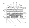
- FIG. 2 is a cross-sectional view of the surface emitting laser 10.
- FIG. 2 is a cross-sectional view taken along the line 2-2 of FIG. The configuration of the surface emitting laser 10 will be described with reference to FIGS. 1 and 2.
- the surface emitting laser 10 is formed so as to be embedded in the mount substrate 10M, the p electrode (connection electrode) 11 formed on the mount substrate 10M, and partially exposed from the p electrode 11. It has 1 multilayer film reflector (hereinafter, simply referred to as a first reflector) 12.
- the first reflecting mirror 12 has a second refractive index higher than that of the first dielectric film (hereinafter referred to as a low refractive index dielectric film) 12L and the low refractive index dielectric film 12L. It has a structure in which the dielectric film (hereinafter referred to as a high refractive index dielectric film) 12H is alternately laminated.
- the first reflector 12 constitutes a distributed Bragg reflector (DBR: Distributed Bragg Reflector) made of a dielectric material.
- DBR Distributed Bragg Reflector
- the p-electrode 11 has an opening on the upper surface that partially exposes the first reflector 12. Further, the first reflecting mirror 12 has an exposed portion 12E that is exposed from the p electrode 11 while protruding from the p electrode 11 at the opening of the p electrode 11.
- the side surface of the lower portion (lower portion in the present embodiment) of the protruding multilayer film portion in the first reflector 12 is covered with the p electrode 11, and the upper portion (in the present embodiment).
- the side surface and the upper surface of the upper portion) protrude from the p electrode 11 and are exposed. That is, in this embodiment, the exposed portion 12E of the first reflecting mirror 12 includes an upper surface of a lower portion of the protruding multilayer film portion and side surfaces and an upper surface of the upper portion. Further, the exposed portion 12E of the first reflecting mirror 12 has a circular shape when viewed from above.
- the surface emitting laser 10 has an insulating layer 14 formed on the p electrode 11 and the translucent electrode 13 and having an opening 14A for exposing the translucent electrode 13 on the exposed portion 12E of the first reflecting mirror 12. Have.
- the translucent electrode 13 has an exposed portion 13E exposed from the opening 14A of the insulating layer 14.
- the exposed portion 13E of the translucent electrode 13 has a circular upper surface shape.
- the surface emitting laser 10 has a photosemiconductor layer 15 formed on the insulating layer 14 and connected to the exposed portion 13E of the translucent electrode 13 at the opening 14A of the insulating layer 14.
- the optical semiconductor layer 15 includes a plurality of semiconductor layers made of nitride-based semiconductors.
- the exposed portion 13E of the translucent electrode 13 functions as a contact region for electrically connecting the translucent electrode 13 (p electrode 11) and the photosemiconductor layer 15.
- the optical semiconductor layer 15 is a p-type semiconductor layer (first semiconductor layer having a first conductive type) 15P formed on the insulating layer 14 while being in contact with the exposed portion 13E of the translucent electrode 13.
- the n-type semiconductor layer 15N has a GaN composition and contains Si as an n-type impurity.
- the light emitting layer 15A has a quantum well structure including a well layer having an InGaN composition and a barrier layer having a GaN composition.
- the p-type semiconductor layer 15P has a GaN-based composition and contains Mg as a p-type impurity.
- the optical semiconductor layer 15 is, for example, an electron block layer (shown) that prevents electrons injected into the light emitting layer 15A from overflowing into the p-type semiconductor layer 15P between the light emitting layer 15A and the p-type semiconductor layer 15P. ) May have.
- the electron block layer may have an AlGaN composition.
- the electron block layer may contain impurities, for example, it may have p-type impurities and may have a p-type conductive type.
- the semiconductor substrate 17 has an n-type conductive type.
- the semiconductor substrate 17 is made of a semiconductor material having n-type impurities, and in this embodiment, it is a GaN substrate containing Si.
- the semiconductor substrate 17 has a top surface 17S and a convex portion 17P protruding from the top surface 17S.
- the convex portion 17P has a top surface 17PS that has been mirrored by polishing.
- the convex portion 17P has a damage layer 17A formed in a region having a predetermined depth from the top surface 17PS and whose conductivity is impaired by polishing.
- the convex portion 17P is a portion of the semiconductor substrate 17 that protrudes in a columnar shape from the upper surface 17S. Further, the convex portion 17P is formed so that the central axis of the convex portion 17P is arranged at a position passing through the center of the exposed portion 13E (that is, the contact region with the photosemiconductor layer 15) of the translucent electrode 13. Further, in this embodiment, the width (diameter) D2 of the convex portion 17P is larger than the width (diameter) D1 of the exposed portion 13E of the translucent electrode 13.
- the upper surface 17S of the semiconductor substrate 17 is a surface region of the semiconductor substrate 17 removed by etching. More specifically, the upper surface 17S of the semiconductor substrate 17 is a surface region of the semiconductor substrate 17 exposed by removing the polished surface by dry etching after polishing. Therefore, the upper surface 17S of the semiconductor substrate 17 is a region showing an n-type conductive type. Further, in this embodiment, the convex portion 17P of the semiconductor substrate 17 is a surface region of the semiconductor substrate 17 in which the polished surface remains without being dry-etched.
- the surface emitting laser 10 has an n electrode (second electrode) 18 formed on the upper surface 17S of the semiconductor substrate 17 and having an opening 18A surrounding the convex portion 17P.
- the n-electrode 18 is made of a metal material such as Au, Al and Cu.
- the n-electrode 18 is formed in a layer on the semiconductor substrate 17. Further, the opening 18A of the n electrode 18 has an opening width larger than the width of the convex portion 17P of the semiconductor substrate 17, and is formed apart from the convex portion 17P.
- the surface emitting laser 10 has an antireflection layer 19 formed on the n electrode 18 so as to embed the convex portion 17P of the semiconductor substrate 17.
- the antireflection layer 19 is made of, for example, a dielectric multilayer film, and in this embodiment, it has a structure in which Ta 2 O 5 layers and SiO 2 layers are alternately laminated a plurality of times.
- the antireflection layer 19 suppresses the light emitted from the light emitting layer 15A from being reflected by the top surface 17PS of the convex portion 17P of the semiconductor substrate 17.
- the exposed portion 13E of the translucent electrode 13 (that is, the opening 14A of the insulating layer 14) defines the light emitting center which is the center of the light emitting region of the light emitting layer 15A, and the central axis of the resonator 10C (hereinafter, hereinafter).
- AX is defined (referred to as the central axis of light emission).
- the light emitting center axis AX of the resonator 10C passes through the center of the exposed portion 13E of the translucent electrode 13 and extends in a direction perpendicular to the photosemiconductor layer 15.
- the light emitting region of the light emitting layer 15A is, for example, a region having a predetermined width in which light having a predetermined intensity or higher is emitted in the light emitting layer 15A, and the center thereof is the light emitting center. Further, for example, the light emitting region of the light emitting layer 15A is a region in which a current having a predetermined density or higher is injected in the light emitting layer 15A, and the center thereof is the light emitting center. Further, a straight line perpendicular to the mount substrate 10M passing through the light emitting center is the light emitting center axis AX.
- the emission center axis AX is a straight line extending along the resonator length direction of the resonator 10C composed of the first reflector 12 and the second reflector 16. Further, the light emission center axis AX corresponds to the optical axis of the laser light emitted from the surface light emitting laser 10.
- the second reflector 16 has a light reflectivity smaller than that of the first reflector 12. Further, the second reflecting mirror 16 has translucency with respect to the light emitted from the light emitting layer 15A. The second reflecting mirror 16 reflects most of the light emitted from the light emitting layer 15A, transmits a part of the laser light LB resonating in the resonator 10C, and emits the light to the outside of the resonator 10C.
- FIG. 3 is a diagram schematically showing a current path in the surface emitting laser 10.
- the current CR flowing between the translucent electrode 13 (p electrode 11) and the n electrode 18 is substantially perpendicular to the photosemiconductor layer 15 and the second reflector 16. It flows along a direction (hereinafter referred to as a vertical direction).
- This current CR path can be said to be the path with the smallest electrical resistance for injecting current into the optical semiconductor layer 15.
- the distance between the electrodes is often less than about 200 ⁇ m. This is because the surface emitting laser 10 itself cannot be handled unless it has a certain level of mechanical strength, and therefore it is necessary to leave a thickness of about 80 to 200 ⁇ m for the semiconductor substrate 17.
- the electric resistance in the optical semiconductor layer 15 is proportional to the distance of the current path flowing in the optical semiconductor layer 15 and inversely proportional to the cross-sectional area of the current path.
- the cross-sectional area of the current path is large enough to cancel out the difference in the distances of the current paths as compared with the case where the electrodes are arranged in the horizontal direction.
- the cross-sectional area of the current path in the case of the vertical electrode arrangement is two orders of magnitude or more larger than the cross-sectional area of the current path in the case of the horizontal electrode arrangement (the cross-sectional area is much more than 100 times). Therefore, by arranging the electrodes in the vertical direction, the electrical resistance between the electrodes can be made much smaller than in the horizontal direction.
- the current CR is injected into the light emitting layer 15A in the optical semiconductor layer 15 without being wasted, and is converted into light with high efficiency. Therefore, the optical semiconductor layer 15 can perform a highly efficient light emitting operation.
- the semiconductor The substrate 17 is preferably thin to some extent.
- the top surface 17PS of the convex portion 17P which is the exit surface of the laser light LB, is highly flattened. It is preferable to have. In this case, for example, it is used that the growth substrate to be the semiconductor substrate 17 is thinned and then mirrored by polishing or the like.
- polishing has the disadvantage of forming a non-conductive region in the vicinity of the polished surface of the growth substrate.
- the inventors of the present application have experimentally confirmed that when the n-electrode 18 is formed on the polished surface, the conduction with the p-electrode 11 cannot be obtained.
- the region of 17S is used as a contact region with the n electrode 18. Therefore, a good vertical current CR path can be formed between the upper surface 17S of the semiconductor substrate 17 and the exposed portion 13E of the translucent electrode 13 with the opto-semiconductor layer 15 interposed therebetween.
- the surface emitting laser 10 is a light emitting element capable of performing highly efficient light emitting operation by performing highly efficient current injection. Further, the surface emitting laser 10 is a laser element capable of emitting a stable high-output laser beam LB. Further, since the antireflection layer 19 is provided on the convex portion 17P, it is possible to more stably emit the laser beam LB having high output and optical characteristics.
- the shape and size of the convex portion 17P on the semiconductor substrate 17 can be designed based on, for example, the beam shape and radiation angle of the laser beam LB.
- the light emitting layer 15A is set as the emission point of the laser beam LB, the distance from the n-type semiconductor layer 15N to the top surface 17PS of the convex portion 17P of the semiconductor substrate 17, the n-type semiconductor layer 15N, and the second reflection.
- the beam shape and beam width (beam diameter) of the laser beam LB on the top surface 17PS of the convex portion 17P of the semiconductor substrate 17 are calculated. be able to.
- the height of the convex portion 17P with respect to the upper surface 17S of the semiconductor substrate 17 is larger than the thickness of the n electrode 18 (height from the upper surface 17S).
- the opening 18A of the n electrode 18 has an opening diameter larger than the width D2 of the convex portion 17P of the semiconductor substrate 17. Therefore, the n electrode 18 is separated from the side surface of the convex portion 17P. This is preferable in the production of the n electrode 18. Specifically, when the metal layer to be the n electrode 18 is formed by lift-off, burrs may occur at the end of the metal layer when the metal layer is lifted off. Even in this case, by forming the n electrode 18 using a mask larger than the convex portion 17P, it is possible to prevent the burr from being formed on the convex portion 17P.
- the p electrode 11 is in contact with almost the entire surface of the mount substrate 10M.
- the p-electrode 11 can form a heat dissipation path that effectively sends the heat generated from the optical semiconductor layer 15 to the mount substrate 10M. Therefore, the surface emitting laser 10 is a light emitting element having high heat dissipation performance and operating stably even when driven for a long time and with a large current.
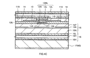
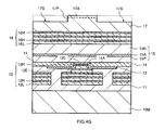
- FIGS. 4A to 4H are cross-sectional views showing a manufacturing process of the surface emitting laser 10. An example of a method for manufacturing the surface emitting laser 10 will be described with reference to FIGS. 4A to 4H.
- FIGS. 4A to 4H is a cross-sectional view similar to that of FIG. 2 in the manufacturing process of the surface emitting laser 10.
- the insulating layer 14 is formed on the optical semiconductor layer 15.
- a SiO 2 layer is formed on the p-type semiconductor layer 15P, and an opening is formed in a part of the SiO 2 layer.
- the insulating layer 14 having the opening 14A is formed.
- the translucent electrode 13 is formed on the insulating layer 14.
- ITO as a translucent electrode 13 is formed in a layer on the insulating layer 14 so as to be in contact with the upper surface of the p-type semiconductor layer 15P at the opening 14A of the insulating layer 14.
- a layered electrode 11A forming a part of the p electrode 11 is formed on the insulating layer 14.
- a metal layer having an opening 11B having an opening width larger than the width D1 of the opening 14A of the insulating layer 14 is formed as the layered electrode 11A.
- the opening 11B of the layered electrode 11A is arranged so as to overlap the opening 14A of the insulating layer 14 when viewed from a direction perpendicular to the layered electrode 11A (so as to surround the opening 14A in this embodiment).
- the growth substrate 17WG after polishing has a very high resistance, and a high resistance region that becomes non-ohmic contact even if the n electrode is formed as it is, that is, a surface region that becomes the damage layer 17A of the semiconductor substrate 17 is formed.
- a part of the dielectric multilayer film 12ML is removed to expose the layered electrode 11A.
- the region where the dielectric multilayer film 12ML is removed in a tubular shape is defined so that the opening 11B of the layered electrode 11A is surrounded by the portion of the layered electrode 11A exposed from the dielectric multilayer film 12ML in an annular shape.
- the semiconductor substrate 17 has a mirrored top surface 17PS on the convex portion 17P and a damage layer 17A having impaired conductivity in the vicinity of the top surface 17PS has been described.
- the configuration of the semiconductor substrate 17 is not limited to this, and the semiconductor substrate 17 may have at least an upper surface 17S on which the n electrode 18 is formed and a convex portion 17P protruding from the upper surface 17S and functioning as a light emitting surface. ..
- the surface emitting laser 10 includes a first reflecting mirror 12, a translucent electrode (first electrode) 13 formed on the first reflecting mirror 12, and a translucent electrode.
- a p-type semiconductor layer 15P (first semiconductor layer) formed on the p-type semiconductor layer 15, a light emitting layer 15A formed on the p-type semiconductor layer 15P, and an n-type semiconductor layer 15N formed on the light emitting layer 15A.
- a second reflector 16 formed on the n-type semiconductor layer 15N and composed of a plurality of semiconductor films having an n-type conductive type (second conductive type) and a second reflecting mirror 16 formed on the upper surface.
- the surface emitting laser 20 includes a first reflector 21 having a plurality of exposed portions 21P, an insulating layer 23 having a plurality of openings 23A corresponding to each of the exposed portions 21P, and a plurality of exposed portions. It has a translucent electrode 22 having 22E and a semiconductor substrate 24 having a plurality of convex portions 24P. That is, the surface emitting laser 20 has a plurality of light emitting portions and has a plurality of light emitting central axes AX.
- the translucent electrode 22 is formed on the first reflecting mirror 21 while covering each of the plurality of exposed portions 21E of the first reflecting mirror 21.
- the insulating layer 23 has an opening 23A that exposes the translucent electrode 22 in the region on the exposed portion 21E of the first reflecting mirror 21 in the translucent electrode 22.
- the translucent electrode 22 has a plurality of exposed portions 22E, each of which is exposed from the insulating layer 23. That is, the p-type semiconductor layer 15P of the opto-semiconductor layer 15 is formed with contact regions with a plurality of translucent electrodes 22.
- the surface emitting laser 20 has an n electrode 25 formed on the upper surface 24S of the semiconductor substrate 24 and having a plurality of openings 25A surrounding each of the plurality of convex portions 24P. Further, the surface emitting laser 20 has an antireflection layer 26 formed so as to cover the convex portion 24P and the n electrode 25 of the semiconductor substrate 24. Further, the surface emitting laser 20 has a pad electrode 27 connected to the n electrode 25.
- the surface emitting laser 20 has a plurality of convex portions 24P of the semiconductor substrate 24 as emission portions of the laser beam LB. Also in this surface emitting laser 20, by using a region other than the convex portion 24P of the semiconductor substrate 24 as a contact region with the n electrode 25, it is possible to form good conduction in the vertical direction, and the optical semiconductor layer 15 can be formed. It is possible to perform highly efficient current injection. Therefore, it is possible to provide a surface emitting laser 20 (vertical resonator type light emitting element) that performs highly efficient light emitting operation by performing highly efficient current injection.
Landscapes
- Physics & Mathematics (AREA)
- Condensed Matter Physics & Semiconductors (AREA)
- General Physics & Mathematics (AREA)
- Electromagnetism (AREA)
- Optics & Photonics (AREA)
- Semiconductor Lasers (AREA)
Abstract
第1の多層膜反射鏡と、第1の多層膜反射鏡上に形成された透光性の第1の電極と、第1の電極上に形成された第1の導電型を有する第1の半導体層と、第1の半導体層上に形成された発光層と、発光層上に形成され、第1の導電型とは反対の第2の導電型を有する第2の半導体層と、第2の半導体層上に形成され、第2の導電型を有する複数の半導体膜からなり、第1の多層膜反射鏡と共に共振器を構成する第2の多層膜反射鏡と、第2の多層膜反射鏡上に形成され、上面及び上面から突出する凸部を有し、第2の導電型を有する半導体基板と、半導体基板の上面上に形成された第2の電極と、を有する。
Description
本発明は、垂直共振器型面発光レーザなどの垂直共振器型発光素子に関する。
従来から、半導体レーザの1つとして、電圧の印加によって光を放出する半導体層と、当該半導体層を挟んで互いに対向する多層膜反射鏡と、を有する垂直共振器型の面発光レーザが知られている。また、当該半導体レーザには、例えば、当該半導体層に電気的に接続された電極が設けられている。例えば、特許文献1には、n型半導体層及びp型半導体層にそれぞれ接続されたn電極及びp電極を有する垂直共振器型の半導体レーザが開示されている。
例えば、面発光レーザなどの垂直共振器型発光素子には、対向する反射鏡によって光共振器が形成されている。例えば、面発光レーザ内においては、電極を介して半導体層に電圧が印加されることで、当該半導体層から放出された光が当該光共振器内で共振し、レーザ光が生成される。
ここで、面発光レーザ内において低閾値でレーザ発振を起こさせるためには、例えば、電極を介して半導体層に注入される電流が半導体層内において高効率で光に変換されることが好ましい。従って、例えば、面発光レーザなどの垂直共振器型発光素子は、半導体層に低抵抗で電流を注入できる電極構成を有することが好ましい。
本発明は上記した点に鑑みてなされたものであり、高効率な電流注入を行うことで高効率な発光動作を行う垂直共振器型発光素子を提供することを目的としている。
本発明による垂直共振器型発光素子は、第1の多層膜反射鏡と、第1の多層膜反射鏡上に形成された透光性の第1の電極と、第1の電極上に形成された第1の導電型を有する第1の半導体層と、第1の半導体層上に形成された発光層と、発光層上に形成され、第1の導電型とは反対の第2の導電型を有する第2の半導体層と、第2の半導体層上に形成され、第2の導電型を有する複数の半導体膜からなり、第1の多層膜反射鏡と共に共振器を構成する第2の多層膜反射鏡と、第2の多層膜反射鏡上に形成され、上面及び上面から突出する凸部を有し、第2の導電型を有する半導体基板と、半導体基板の上面上に形成された第2の電極と、を有することを特徴としている。
以下、本発明の実施例について詳細に説明する。また、以下の実施例においては、本発明が面発光レーザ(半導体レーザ)として実施される場合について説明する。しかし、本発明は、面発光レーザに限定されず、垂直共振器型発光ダイオードなど、種々の垂直共振器型発光素子に適用することができる。
図1は、実施例1に係る垂直共振器型面発光レーザ(VCSEL:Vertical Cavity Surface Emitting Laser、以下、面発光レーザと称する)の模式的な上面図である。また、図2は、面発光レーザ10の断面図である。図2は、図1の2-2線に沿った断面図である。図1及び図2を用いて、面発光レーザ10の構成について説明する。
面発光レーザ10は、マウント基板10Mと、マウント基板10M上に形成されたp電極(接続電極)11と、p電極11に埋め込まれて部分的にp電極11から露出するように形成された第1の多層膜反射鏡(以下、単に第1の反射鏡と称する)12と、を有する。
本実施例においては、第1の反射鏡12は、第1の誘電体膜(以下、低屈折率誘電体膜と称する)12Lと低屈折率誘電体膜12Lよりも高い屈折率を有する第2の誘電体膜(以下、高屈折率誘電体膜と称する)12Hとが交互に積層された構造を有する。本実施例においては、第1の反射鏡12は、誘電体材料からなる分布ブラッグ反射器(DBR:Distributed Bragg Reflector)を構成する。
また、本実施例においては、p電極11は、上面に第1の反射鏡12を部分的に露出させる開口部を有する。また、第1の反射鏡12は、p電極11の当該開口部においてp電極11から突出しつつp電極11から露出する露出部12Eを有する。
本実施例においては、第1の反射鏡12は、p電極11に埋め込まれた埋設多層膜部分と、当該埋設多層膜部分から段階的に幅が小さくなるように突出する突出多層膜部分と、を有する。本実施例においては、当該突出多層膜部分は、2段階で直径が小さくなるように当該埋設多層膜部分から円柱状に突出した第1の反射鏡12の部分である。
また、本実施例においては、第1の反射鏡12における当該突出多層膜部分の下方部分(本実施例においては下段部)の側面はp電極11に覆われ、上方部分(本実施例においては上段部)の側面及び上面はp電極11から突出して露出している。すなわち、本実施例においては、第1の反射鏡12の露出部12Eは、当該突出多層膜部分の下方部分の上面と、上方部分の側面及び上面と、を含む。また、第1の反射鏡12の露出部12Eは、上面視において円形状を有する。
面発光レーザ10は、第1の反射鏡12の露出部12Eを覆いつつp電極11上に形成された透光電極(第1の電極)13を有する。本実施例においては、第1の反射鏡12は、マウント基板10M側から透光電極13側に至る貫通孔を有する。また、p電極11は、第1の反射鏡12を部分的に貫通して透光電極13に接続されている。また、本実施例においては、第1の反射鏡12は筒状に形成された貫通孔を有し、p電極11は筒状に第1の反射鏡12を貫通して透光電極13に接続されている。
また、面発光レーザ10は、p電極11及び透光電極13上に形成され、かつ第1の反射鏡12の露出部12E上において透光電極13を露出させる開口部14Aを有する絶縁層14を有する。
本実施例においては、透光電極13は、絶縁層14の開口部14Aから露出する露出部13Eを有する。本実施例においては、透光電極13の露出部13Eは、円形の上面形状を有する。
例えば、マウント基板10Mは、熱伝導性の高い材料、例えばAlNなどのセラミックス材料からなる。p電極11は、Au、Al及びCuなどの金属材料からなる。第1の反射鏡12における低屈折率誘電体膜12LはSiO2からなり、高屈折率誘電体膜12HはNb2O5からなる。透光電極13は、ITO及びIZOなどの透明導電膜からなる。また、絶縁層14は、SiO2及びSiNなどからなる。
面発光レーザ10は、絶縁層14上に形成され、かつ絶縁層14の開口部14Aにおいて透光電極13の露出部13Eに接続された光半導体層15を有する。例えば、光半導体層15は、窒化物系半導体からなる複数の半導体層を含む。透光電極13の露出部13Eは、透光電極13(p電極11)と光半導体層15とを電気的に接続するコンタクト領域として機能する。
本実施例においては、光半導体層15は、透光電極13の露出部13Eに接しつつ絶縁層14上に形成されたp型半導体層(第1の導電型を有する第1の半導体層)15Pと、p型半導体層15P上に形成された発光層(活性層)15Aと、発光層15A上に形成されたn型半導体層(第2の半導体層、第1の導電型とは反対の第2の導電型を有する半導体層)15Nと、を有する。
本実施例においては、n型半導体層15Nは、GaNの組成を有し、Siをn型不純物として含む。発光層15Aは、InGaNの組成を有する井戸層及びGaNの組成を有する障壁層を含む量子井戸構造を有する。また、p型半導体層15Pは、GaN系の組成を有し、Mgをp型不純物として含む。
なお、光半導体層15の構成はこれに限定されない。例えば、n型半導体層15Nは、互いに組成が異なる複数のn型の半導体層を有していてもよい。また、発光層15Aは、単一量子井戸構造を有していてもよいし、単層構造を有していてもよい。
また、p型半導体層15Pは、互いに組成が異なる複数のp型の半導体層を有していてもよい。例えば、p型半導体層15Pは、透光電極13とのオーミックコンタクトを形成するためのコンタクト層(図示せず)を有していてもよい。この場合、例えば、p型半導体層15Pは、当該コンタクト層と発光層15Aとの間に、クラッド層としてのGaN層を有していればよい。
また、光半導体層15は、例えば、発光層15Aとp型半導体層15Pとの間に、発光層15Aに注入された電子のp型半導体層15Pへのオーバーフローを防止する電子ブロック層(図示せず)を有していてもよい。例えば、当該電子ブロック層は、AlGaNの組成を有していてもよい。また、当該電子ブロック層は、不純物を含んでいてもよく、例えばp型の不純物を有し、p型の導電型を有していてもよい。
面発光レーザ10は、光半導体層15上に形成された第2の多層膜反射鏡(以下、単に第2の反射鏡と称する)16を有する。第2の反射鏡16は、光半導体層15を挟んで第1の反射鏡12に対向して配置されている。第2の反射鏡16は、第1の反射鏡12と共に、光半導体層15に垂直な方向(マウント基板10Mに垂直な方向)を共振器長方向とする共振器10Cを構成する。
本実施例においては、第2の反射鏡16は、第1の半導体膜(以下、低屈折率半導体膜と称する)16Lと低屈折率半導体膜16Lよりも高い屈折率を有する第2の半導体膜(以下、高屈折率半導体膜と称する)16Hとが交互に積層された構造を有する。すなわち、本実施例においては、第2の反射鏡16は、半導体材料からなる分布ブラッグ反射器を構成する。
例えば、第2の反射鏡16における低屈折率半導体膜16L及び高屈折率半導体膜16Hの各々は、光半導体層15と同種の半導体材料、本実施例においては窒化物系半導体材料からなる。例えば、低屈折率半導体膜16LはAlInNからなり、高屈折率半導体膜16HはGaNからなる。
また、本実施例においては、第2の反射鏡16は、n型の導電型を有する。本実施例においては、低屈折率半導体膜16L及び高屈折率半導体膜16Hの各々は、n型不純物を含む。例えば、本実施例においては、低屈折率半導体膜16L及び高屈折率半導体膜16Hは、それぞれSiを含むAlInN膜及びGaN膜である。
面発光レーザ10は、第2の反射鏡16上に形成された半導体基板17を有する。半導体基板17は、光半導体層15及び第2の反射鏡16と同種の半導体材料、本実施例においては窒化物系半導体材料からなる。半導体基板17は、発光層15Aから放出された光に対して透光性を有する。
また、本実施例においては、半導体基板17は、光半導体層15及び第2の反射鏡16の結晶成長に用いられる成長用基板である。例えば、半導体基板17は、GaNの組成を有する。また、本実施例においては、半導体基板17と第2の反射鏡16との間にはGaNの組成を有するバッファ層(図示せず)を有する。
また、本実施例においては、半導体基板17は、n型の導電型を有する。本実施例においては、半導体基板17は、n型不純物を有する半導体材料からなり、本実施例においてはSiを含むGaN基板である。
また、半導体基板17は、上面17S及び上面17Sから突出した凸部17Pを有する。凸部17Pは、研磨されることで鏡面化された頂面17PSを有する。また、凸部17Pは、頂面17PSから所定の深さの領域に形成され、研磨されることで導電性が損なわれたダメージ層17Aを有する。
本実施例においては、凸部17Pは、半導体基板17における上面17Sから円柱状に突出した部分である。また、凸部17Pは、凸部17Pの中心軸が透光電極13における露出部13E(すなわち光半導体層15とのコンタクト領域)の中心を通る位置に配置されるように、形成されている。また、本実施例においては、凸部17Pの幅(直径)D2は、透光電極13の露出部13Eの幅(直径)D1よりも大きい。
また、本実施例においては、半導体基板17の上面17Sは、エッチングによって除去された半導体基板17の表面領域である。より具体的には、半導体基板17の上面17Sは、研磨された後にドライエッチングによって当該研磨面が除去されて表出した半導体基板17の表面領域である。従って、半導体基板17の上面17Sは、n型の導電型を示す領域である。また、本実施例においては、半導体基板17の凸部17Pは、ドライエッチングされずに研磨面が残存した半導体基板17の表面領域である。
面発光レーザ10は、半導体基板17の上面17S上に形成され、凸部17Pを囲む開口部18Aを有するn電極(第2の電極)18を有する。本実施例においては、n電極18は、Au、Al及びCuなどの金属材料からなる。
また、本実施例においては、n電極18は、半導体基板17上に層状に形成されている。また、n電極18の開口部18Aは、半導体基板17の凸部17Pの幅よりも大きな開口幅を有し、凸部17Pから離間して形成されている。
面発光レーザ10は、半導体基板17の凸部17Pを埋設するようにn電極18上に形成された反射防止層19を有する。反射防止層19は、例えば、誘電体多層膜からなり、本実施例においては、Ta2O5層及びSiO2層が複数回交互に積層された構造を有する。反射防止層19は、発光層15Aから放出された光が半導体基板17の凸部17Pの頂面17PSで反射することを抑制する。
本実施例においては、透光電極13の露出部13E(すなわち絶縁層14の開口部14A)は、発光層15Aの発光領域の中心である発光中心を画定し、共振器10Cの中心軸(以下、発光中心軸と称する)AXを画定する。共振器10Cの発光中心軸AXは、透光電極13の露出部13Eの中心を通り、光半導体層15に垂直な方向に沿って延びる。
なお、発光層15Aの発光領域とは、例えば、発光層15A内における所定の強度以上の光が放出される所定の幅の領域であり、その中心が発光中心である。また、例えば、発光層15Aの発光領域とは、発光層15A内において所定の密度以上の電流が注入される領域であり、その中心が発光中心である。また、当該発光中心を通るマウント基板10Mに垂直な直線が発光中心軸AXである。発光中心軸AXは、第1の反射鏡12及び第2の反射鏡16によって構成される共振器10Cの共振器長方向に沿って延びる直線である。また、発光中心軸AXは、面発光レーザ10から出射されるレーザ光の光軸に対応する。
また、本実施例においては、第2の反射鏡16は、第1の反射鏡12よりも小さな光反射性を有する。また、第2の反射鏡16は、発光層15Aから放出された光に対して透光性を有する。第2の反射鏡16は、発光層15Aから放出された光の大部分を反射させ、かつ共振器10C内で共振したレーザ光LBの一部を透過させて共振器10Cの外側に出射する。
従って、本実施例においては、面発光レーザ10は、共振器10C内に生成されるレーザ光LBを半導体基板17の凸部17Pの頂面17PSから出射するように構成されている。
換言すれば、面発光レーザ10は、半導体基板17の凸部17Pの領域を光取り出し領域として有し、半導体基板17の凸部17Pの周囲の領域である上面17Sの領域(凸部17Pに対する凹部領域と称することもできる)を光半導体層15へのコンタクト領域として有する。
図3は、面発光レーザ10内の電流経路を模式的に示す図である。本実施例においては、図3の破線に示すように、透光電極13(p電極11)及びn電極18間に流れる電流CRは、ほぼ光半導体層15及び第2の反射鏡16に垂直な方向(以下、縦方向と称する)に沿って流れる。この電流CRの経路は、光半導体層15に電流を注入する上で最も電気抵抗が小さくなる経路といえる。
具体的には、まず、面発光レーザ10のように、縦方向において対向する電極を配置した場合、電極間の距離は、約200μm未満となる場合が多い。これは、面発光レーザ10自体にある程度の機械的強度がなければハンドリングできないため、半導体基板17の厚みとして、概ね80~200μm程度を残す必要があるためである。
一方、仮に、光半導体層15を部分的に除去するなどし、光半導体層15に平行な方向(以下、横方向と称する)に電極を配置した場合、電流は、光半導体層15に平行な方向に流れることとなる。また、この場合、安定した放熱特性や電気的特性を考慮すると、当該電極間の電流経路の距離は約50μm以上となる場合が多い。
ここで、光半導体層15内の電気抵抗は、光半導体層15内を流れる電流経路の距離に比例し、電流経路の断面積に反比例する。そして、縦方向に電極を配置する場合、電流経路の断面積は、横方向に電極を配置する場合に比べて、電流経路の距離の差を打ち消すほど大きい。例えば、縦方向の電極配置の場合の電流経路の断面積は、横方向の電極配置の場合の電流経路の断面積よりも2桁以上大きい(100倍を大きく超える断面積である)。従って、縦方向に電極を配置することで、電極間の電気抵抗を横方向の場合よもはるかに小さくすることができる。
従って、電流CRは、光半導体層15内において、無駄になることなく、発光層15Aに注入され、高効率で光に変換されることとなる。従って、光半導体層15は、高効率な発光動作を行うことができる。
また、本実施例においては、レーザ光LBは、鏡面化された半導体基板17の凸部17Pの頂面17PSから出射する。これは、レーザ光LBの出力及びビーム形状を安定させる上で最も好ましい構成となる。
具体的には、面発光レーザ10のように縦方向に電極を配置する場合において、高い電気的特性を得ること、及びレーザ光LBが出力を低下させずに出射されることを考慮すると、半導体基板17はある程度薄い方が好ましい。
また、レーザ光LBのビーム形状や出力分布など、レーザ光LBの光学特性を安定させることを考慮すると、レーザ光LBの出射面である凸部17Pの頂面17PSは、高度に平坦化されていることが好ましい。この場合、例えば、半導体基板17となる成長用基板を薄くする加工を行った上で、研磨などの鏡面化処理を行うことが用いられる。
しかし、本願の発明者らは、研磨を行うことによって、成長用基板の研磨面の近傍に導電性を有さない領域が形成されるというデメリットを有することに着目した。また、本願の発明者らは、研磨面上にn電極18を形成した場合、p電極11との導通がとれなかったことを実験によって確認した。
これに対し、本実施例においては、光出射面となる部分を除いて成長用基板の研磨面を除去することで、レーザ光LBの光路となる部分以外の半導体基板17の表面領域である上面17Sの領域をn電極18とのコンタクト領域として用いる。従って、光半導体層15を挟んで、半導体基板17の上面17Sと透光電極13の露出部13Eとの間で、良好な縦方向の電流CRの経路を形成することができる。
従って、面発光レーザ10は、高効率な電流注入を行うことで高効率な発光動作を行うことが可能な発光素子となる。また、面発光レーザ10は、安定した高出力なレーザ光LBを出射することが可能なレーザ素子となる。また、凸部17P上に反射防止層19が設けられていることで、より安定して高い出力及び光学特性のレーザ光LBを出射することができる。
なお、半導体基板17における凸部17Pの形状及びサイズなどは、例えば、レーザ光LBのビーム形状、放射角などに基づいて設計することができる。例えば、発光層15Aをレーザ光LBの出射点とし、n型半導体層15Nからレーザ光LBが半導体基板17の凸部17Pの頂面17PSまでの距離と、n型半導体層15N、第2の反射鏡16及び半導体基板17内でのレーザ光LBの放射角と、を考慮すると、半導体基板17の凸部17Pの頂面17PSでのレーザ光LBのビーム形状及びビーム幅(ビーム径)を算出することができる。
また、本実施例においては、半導体基板17における上面17Sに対する凸部17Pの高さは、n電極18の厚さ(上面17Sからの高さ)よりも大きい。これによって、レーザ光LBが凸部17Pの頂面17PSから出射された後に、当該レーザ光LBの外縁部がn電極18によって吸収されることが抑制される。従って、レーザ光LBを設計上のビーム形状及び出力で安定して出射することができる。
また、本実施例においては、n電極18の開口部18Aは、半導体基板17の凸部17Pの幅D2よりも大きい開口径を有する。従って、n電極18は、凸部17Pの側面から離間している。これは、n電極18の製造上好ましい。具体的には、n電極18となる金属層をリフトオフによって形成する場合において、当該金属層をリフトオフする際に当該金属層の端部にバリが発生する場合がある。この場合においても、凸部17Pよりも大きなマスクを用いてn電極18を形成することで、当該バリが凸部17P上に形成されることを抑制することができる。
また、本実施例においては、p電極11がマウント基板10Mのほぼ全面に接している。これによって、p電極11は、光半導体層15から発生する熱を効果的にマウント基板10Mに送る放熱経路を形成することができる。従って、面発光レーザ10は、高い放熱性能を有し、長時間及び大電流で駆動した場合でも安定して動作する発光素子となる。
また、本実施例においては、p電極11は、第1の反射鏡12を貫通して透光電極13に接続されている。従って、光半導体層15からの熱を効果的にマウント基板10Mに送る経路を形成することができる。また、p電極11は、発光中心軸AXを包むように筒状に第1の反射鏡12を貫通するように形成されている。これによって、大きな放熱効果が期待できる。
図4A~図4Hの各々は、面発光レーザ10の製造過程を示す断面図である。図4A~図4Hを用いて、面発光レーザ10の製造方法の例について説明する。なお、図4A~図4Hの各々は、面発光レーザ10の製造過程における図2と同様の断面図である。
まず、図4Aに示すように、半導体基板17となる成長用基板17Wを準備し、成長用基板17W上に第2の反射鏡16、光半導体層15を成長させる。例えば、第2の反射鏡16及び光半導体層15の成長には、有機金属気相成長法(MOCVD法)を用いることができる。
具体的には、まず、成長用基板17Wとして平板状のn型のGaN基板を準備した。また、当該GaN基板上にバッファ層としてのn-GaN層を成長させた後、当該バッファ層上に高屈折率半導体膜16Hとしてのn-GaN膜及び低屈折率半導体膜16Lとしてのn-AlInN膜を交互に複数回成長させる。これによって、成長用基板17W上に第2の反射鏡16が形成される。
次に、第2の反射鏡16上に、n型半導体層15Nとしてのn-GaN層、発光層15Aとしての複数ペアのInGaN層及びGaN層、並びにp型半導体層15Pとしてのp-GaN層をそれぞれ成長させる。これによって、第2の反射鏡16上に光半導体層15が形成される。
続いて、光半導体層15上に絶縁層14を形成する。本実施例においては、p型半導体層15P上に、SiO2層を形成し、当該SiO2層の一部に開口部を形成した。これによって、開口部14Aを有する絶縁層14が形成される。
次に、絶縁層14上に透光電極13を形成する。本実施例においては、絶縁層14の開口部14Aにおいてp型半導体層15Pの上面に接するように、絶縁層14上に透光電極13としてのITOを層状に形成した。
続いて、絶縁層14上にp電極11の一部をなす層状電極11Aを形成する。本実施例においては、層状電極11Aとして、絶縁層14の開口部14Aの幅D1よりも大きな開口幅の開口部11Bを有する金属層を形成した。層状電極11Aの開口部11Bは、層状電極11Aに垂直な方向から見たときに絶縁層14の開口部14Aに重なるように(本実施例においては開口部14Aを取り囲むように)配置した。
次に、図4Bに示すように、成長用基板17Wの第2の反射鏡16とは反対側の表面から成長用基板17Wを切削及び研磨する。具体的には、まず、成長用基板17Wを切削又は切断し、成長用基板17Wの厚さを小さくする。そして、当該切削面に対し、研削及び研磨処理を行う。これによって、成長用基板17Wにおける第2の反射鏡16とは反対側の面が鏡面化された成長用基板17WGが形成される。
ここで、成長用基板17Wの研磨処理を行うことで、当該研磨された面の近傍においては、n型の導電性が損なわれる。従って、研磨後の成長用基板17WGには、非常に抵抗が高く、そのままn電極を形成しても非オーミック接触となる高抵抗領域、すなわち半導体基板17のダメージ層17Aとなる表面領域が形成される。
続いて、図4Cに示すように、開口部11Bを埋め込むように、層状電極11A上に、第1の反射鏡12となる高屈折率誘電体膜12H及び低屈折率誘電体膜12Lからなる誘電体多層膜12MLを形成する。本実施例においては、高屈折率誘電体膜12H及び低屈折率誘電体膜12Lとして、それぞれNb2O5膜及びSiO2膜Nb2O5を交互に複数回積層した。
次に、図4Dに示すように、誘電体多層膜12MLの一部を除去し、層状電極11Aを露出させる。本実施例においては、層状電極11Aの開口部11Bが層状電極11Aの当該誘電体多層膜12MLから露出した部分によって環状に囲まれるように、誘電体多層膜12MLが筒状に除去された領域を形成する。
また、本実施例においては、層状電極11Aの当該誘電体多層膜12MLから露出した部分が透光電極13上の領域に配置されるように、誘電体多層膜12MLを除去する。誘電体多層膜12MLを部分的に除去することで、層状電極11A上に第2の反射鏡16が形成される。
続いて、図4Eに示すように、第2の反射鏡16を埋設するように、かつ第2の反射鏡16から露出した層状電極11Aに接するように、p電極11をなす埋設電極11Cを形成する。また、埋設電極11Cの上面を平坦化する。埋設電極11Cは、例えば層状電極11Aと同様の金属材料からなる。これによって、層状電極11A及び埋設電極11Cの全体は、部分的に第2の反射鏡16を露出させつつ第2の反射鏡16を埋設するp電極11となる。
次に、図4Fに示すように、p電極11側から成長用基板17WGをマウント基板10Mに接合する。例えば、マウント基板10Mとしてセラミックス基板を準備し、当該セラミックス基板の上面に金属層(図示せず)を形成した後、p電極11を当該金属層に接合する。これによって、マウント基板10Mに、光半導体層15、第1の反射鏡12及び第2の反射鏡16と共に成長用基板11WGが搭載される。
続いて、図4Gに示すように、成長用基板17WGをダメージ領域17DA側から部分的に除去する。例えば、成長用基板17WGの当該部分的な除去には、ドライエッチングなどの加工技術を用いることができる。これによって、成長用基板17WGの当該除去されなかった部分は、当該除去されて露出した表面から突出することとなる。
また、当該除去されなかった部分には、ダメージ領域17DAが残存することとなる。一方、当該除去された部分は、ダメージ領域17DAを有さず、n型の導電型を示す部分となる。これによって、上面17S及び上面17Sから突出した凸部17Pを有し、凸部17Pの上面にダメージ層17Aを有する半導体基板17が形成される。
次に、図4Hに示すように、半導体基板17上に金属層を形成し、当該金属層に凸部17Pを露出させる開口部を形成する。これによって、n電極18が形成される。また、半導体基板17の凸部17Pを埋め込みつつn電極18上に誘電体の多層膜を形成することで、反射防止層19が形成される。面発光レーザ10は、例えばこのようにして作製されることができる。
なお、本実施例においては、半導体基板17が凸部17Pに鏡面化された頂面17PSを有し、頂面17PSの近傍に導電性が損なわれたダメージ層17Aを有する場合について説明した。しかし、半導体基板17の構成はこれに限定されない、半導体基板17は、少なくともn電極18が形成される上面17S及び上面17Sから突出して光出射面として機能する凸部17Pを有していればよい。これによって、半導体基板17を介した縦方向の導通と凸部17Pからの良好な光出射を行うことができる。
また、本実施例においては、半導体基板17における凸部17P以外の表面領域である上面17Sがドライエッチングによって表出した半導体基板17の表面領域である場合について説明した。しかし、半導体基板17の上面17Sは、n型の導電型を示す表面領域であればよく、その形成方法はエッチングに限定されない。
また、本実施例においては、第1の反射鏡12は、p電極11に埋め込まれるように形成されており、p電極11から突出して露出する露出部12Eを有する場合について説明した。また、透光電極13がp電極11に接続されている場合について説明した。しかし、p電極11、第1の反射鏡12及び透光電極13の構成はこれに限定されない。
例えば、面発光レーザ10は、少なくとも第1の反射鏡12及び第1の反射鏡12上に形成されたp側電極として機能する透光電極13を有していればよい。また、透光電極13上に絶縁層14が設けられている場合について説明した。しかし、絶縁層14は設けられていなくてもよい。例えば、p型半導体層15Pにおける透光電極13上の領域の一部が低抵抗化されていれば、この領域が電流注入領域として機能する。また、反射防止層19は、設けられていなくてもよい。
このように、本実施例においては、面発光レーザ10は、第1の反射鏡12と、第1の反射鏡12上に形成された透光電極(第1の電極)13と、透光電極13上に形成されたp型半導体層15P(第1の半導体層)と、p型半導体層15P上に形成された発光層15Aと、発光層15A上に形成されたn型半導体層15Nと、n型半導体層15N上に形成され、n型の導電型(第2の導電型)を有する複数の半導体膜からなる第2の反射鏡16と、第2の反射鏡16上に形成され、上面17S及び上面17Sから突出した凸部17Pを有し、かつn型の導電型を有する半導体基板17と、半導体基板17の上面17S上に形成されたn電極18と、を有する。従って、高効率な電流注入を行うことで高効率な発光動作を行う面発光レーザ10(垂直共振器型発光素子)を提供することができる。
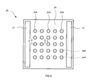
図5は、実施例2に係る面発光レーザ20の上面図である。また、図6は、図5の6-6線に沿った断面図であり、面発光レーザ20の断面図である。図5及び図6を用いて、面発光レーザ20の構成について説明する。
本実施例においては、面発光レーザ20は、複数の露出部21Pを有する第1の反射鏡21、当該露出部21Pの各々に対応する複数の開口部23Aを有する絶縁層23、複数の露出部22Eを有する透光電極22、及び複数の凸部24Pを有する半導体基板24を有する。すなわち、面発光レーザ20は、複数の光出射部を有し、複数の発光中心軸AXを有する。
より具体的には、第1の反射鏡21は、第1の反射鏡12における低屈折率誘電体膜12L及び高屈折率誘電体膜12Hとそれぞれ同様の低屈折率誘電体膜21L及び高屈折率誘電体膜21Hが交互に積層された構造を有する。また、第1の反射鏡21は、各々がp電極11から露出した複数の露出部21Eを有する。本実施例においては、第1の反射鏡21が第2の反射鏡16と共に共振器20Cを構成する。
また、透光電極22は、第1の反射鏡21の複数の露出部21Eの各々を覆いつつ第1の反射鏡21上に形成されている。また、絶縁層23は、透光電極22における第1の反射鏡21の露出部21E上の領域において透光電極22を露出させる開口部23Aを有する。これによって、透光電極22は、各々が絶縁層23から露出する複数の露出部22Eを有する。すなわち、光半導体層15のp型半導体層15Pには、複数の透光電極22とのコンタクト領域が形成されている。
また、半導体基板24は、上面24Sと、透光電極22の複数の露出部22E上にそれぞれ形成されかつ各々が上面24Sから露出した複数の凸部24Pと、を有する。また、凸部24Pの各々は、上面の近傍にダメージ層24Aを有する。
また、面発光レーザ20は、半導体基板24の上面24S上に形成され、複数の凸部24Pをそれぞれ囲む複数の開口部25Aを有するn電極25を有する。また、面発光レーザ20は、半導体基板24の凸部24P及びn電極25を覆うように形成された反射防止層26を有する。また、面発光レーザ20は、n電極25に接続されたパッド電極27を有する。
本実施例においては、面発光レーザ20は、半導体基板24の複数の凸部24Pをレーザ光LBの出射部として有する。この面発光レーザ20においても、半導体基板24の凸部24P以外の領域をn電極25とのコンタクト領域として使用することで、縦方向の良好な導通を形成することが可能となり、光半導体層15に対して高効率な電流注入を行うことが可能となる。従って、高効率な電流注入を行うことで高効率な発光動作を行う面発光レーザ20(垂直共振器型発光素子)を提供することができる。
10、20 面発光レーザ(垂直共振器型発光素子)
11 p電極(接続電極)
12、21 第1の反射鏡
13、22 透光電極(第1の電極)
15 光半導体層
16 第2の反射鏡
17、24 半導体基板
18、25 n電極
11 p電極(接続電極)
12、21 第1の反射鏡
13、22 透光電極(第1の電極)
15 光半導体層
16 第2の反射鏡
17、24 半導体基板
18、25 n電極
Claims (9)
- 第1の多層膜反射鏡と、
前記第1の多層膜反射鏡上に形成された透光性の第1の電極と、
前記第1の電極上に形成された第1の導電型を有する第1の半導体層と、
前記第1の半導体層上に形成された発光層と、
前記発光層上に形成され、前記第1の導電型とは反対の第2の導電型を有する第2の半導体層と、
前記第2の半導体層上に形成され、前記第2の導電型を有する複数の半導体膜からなり、前記第1の多層膜反射鏡と共に共振器を構成する第2の多層膜反射鏡と、
前記第2の多層膜反射鏡上に形成され、上面及び前記上面から突出する凸部を有し、前記第2の導電型を有する半導体基板と、
前記半導体基板の前記上面上に形成された第2の電極と、を有することを特徴とする垂直共振器型発光素子。 - 前記半導体基板の前記凸部は、研磨されることで鏡面化された頂面を有することを特徴とする請求項1に記載の垂直共振器型発光素子。
- 前記半導体基板の前記凸部は、前記頂面の近傍に形成され、当該研磨されることで前記第2の導電型が損なわれたダメージ層を有することを特徴とする請求項2に記載の垂直共振器型発光素子。
- 前記半導体基板の前記上面は、当該研磨された後に当該研磨面がエッチングによって除去された前記半導体基板の表面領域であることを特徴とする請求項2又は3に記載の垂直共振器型発光素子。
- 前記第2の多層膜反射鏡は、前記発光層から放出された光に対して前記第1の多層膜反射鏡よりも小さな反射率を有することを特徴とする請求項1乃至4のいずれか1つに記載の垂直共振器型発光素子。
- 前記第1の多層膜反射鏡を埋め込むように前記第1の多層膜反射鏡上に形成され、前記第1の電極に接続された接続電極を有することを特徴とする請求項1乃至5のいずれか1つに記載の垂直共振器型発光素子。
- 前記接続電極は、前記第1の多層膜反射鏡を貫通して前記第1の電極に接続されていることを特徴とする請求項6に記載の垂直共振器型発光素子。
- 前記半導体基板の前記凸部を覆うように形成された反射防止層を有することを特徴とする請求項1乃至7のいずれか1つに記載の垂直共振器型発光素子。
- 前記第2の電極は、前記凸部から離間して形成されている請求項1乃至8のいずれか1つに記載の垂直共振器型発光素子。
Priority Applications (3)
| Application Number | Priority Date | Filing Date | Title |
|---|---|---|---|
| US17/633,486 US20220285917A1 (en) | 2019-08-08 | 2020-07-15 | Vertical cavity light-emitting element |
| EP20850937.2A EP4012855B1 (en) | 2019-08-08 | 2020-07-15 | Vertical resonator type light emitting element |
| CN202080056286.9A CN114207969B (zh) | 2019-08-08 | 2020-07-15 | 垂直谐振器型发光元件 |
Applications Claiming Priority (2)
| Application Number | Priority Date | Filing Date | Title |
|---|---|---|---|
| JP2019-146049 | 2019-08-08 | ||
| JP2019146049A JP7330805B2 (ja) | 2019-08-08 | 2019-08-08 | 垂直共振器型発光素子 |
Publications (1)
| Publication Number | Publication Date |
|---|---|
| WO2021024719A1 true WO2021024719A1 (ja) | 2021-02-11 |
Family
ID=74503115
Family Applications (1)
| Application Number | Title | Priority Date | Filing Date |
|---|---|---|---|
| PCT/JP2020/027475 Ceased WO2021024719A1 (ja) | 2019-08-08 | 2020-07-15 | 垂直共振器型発光素子 |
Country Status (5)
| Country | Link |
|---|---|
| US (1) | US20220285917A1 (ja) |
| EP (1) | EP4012855B1 (ja) |
| JP (1) | JP7330805B2 (ja) |
| CN (1) | CN114207969B (ja) |
| WO (1) | WO2021024719A1 (ja) |
Families Citing this family (3)
| Publication number | Priority date | Publication date | Assignee | Title |
|---|---|---|---|---|
| TWI674071B (zh) | 2014-12-15 | 2019-10-11 | 瑞士商菲利浦莫里斯製品股份有限公司 | 氣溶膠產生系統及用於在電熱式氣溶膠產生系統內導引氣流的方法 |
| JP2025086542A (ja) * | 2023-11-28 | 2025-06-09 | キヤノン株式会社 | 光源装置及び測距装置 |
| CN120184737B (zh) * | 2025-05-22 | 2025-07-29 | 杭州开幕光子技术有限公司 | 垂直腔面发射激光器及制备方法、激光雷达系统及其光源 |
Citations (5)
| Publication number | Priority date | Publication date | Assignee | Title |
|---|---|---|---|---|
| JP2015126040A (ja) * | 2013-12-26 | 2015-07-06 | 株式会社リコー | 発光デバイス、光源装置及びレーザ装置 |
| US20150311673A1 (en) * | 2014-04-29 | 2015-10-29 | Princeton Optronics Inc. | Polarization Control in High Peak Power, High Brightness VCSEL |
| WO2017047317A1 (ja) * | 2015-09-15 | 2017-03-23 | ソニー株式会社 | 面発光レーザ |
| JP2017098328A (ja) | 2015-11-19 | 2017-06-01 | 学校法人 名城大学 | 垂直共振器型発光素子 |
| JP2017212270A (ja) * | 2016-05-24 | 2017-11-30 | スタンレー電気株式会社 | 面発光レーザ装置 |
Family Cites Families (3)
| Publication number | Priority date | Publication date | Assignee | Title |
|---|---|---|---|---|
| JP3990846B2 (ja) * | 1999-08-27 | 2007-10-17 | キヤノン株式会社 | 面型光素子、その製造方法、およびこれを用いた装置 |
| US6888871B1 (en) * | 2000-07-12 | 2005-05-03 | Princeton Optronics, Inc. | VCSEL and VCSEL array having integrated microlenses for use in a semiconductor laser pumped solid state laser system |
| JP6479308B2 (ja) * | 2013-08-09 | 2019-03-06 | ソニー株式会社 | 面発光レーザ素子及びその製造方法 |
-
2019
- 2019-08-08 JP JP2019146049A patent/JP7330805B2/ja active Active
-
2020
- 2020-07-15 EP EP20850937.2A patent/EP4012855B1/en active Active
- 2020-07-15 US US17/633,486 patent/US20220285917A1/en not_active Abandoned
- 2020-07-15 CN CN202080056286.9A patent/CN114207969B/zh active Active
- 2020-07-15 WO PCT/JP2020/027475 patent/WO2021024719A1/ja not_active Ceased
Patent Citations (5)
| Publication number | Priority date | Publication date | Assignee | Title |
|---|---|---|---|---|
| JP2015126040A (ja) * | 2013-12-26 | 2015-07-06 | 株式会社リコー | 発光デバイス、光源装置及びレーザ装置 |
| US20150311673A1 (en) * | 2014-04-29 | 2015-10-29 | Princeton Optronics Inc. | Polarization Control in High Peak Power, High Brightness VCSEL |
| WO2017047317A1 (ja) * | 2015-09-15 | 2017-03-23 | ソニー株式会社 | 面発光レーザ |
| JP2017098328A (ja) | 2015-11-19 | 2017-06-01 | 学校法人 名城大学 | 垂直共振器型発光素子 |
| JP2017212270A (ja) * | 2016-05-24 | 2017-11-30 | スタンレー電気株式会社 | 面発光レーザ装置 |
Non-Patent Citations (1)
| Title |
|---|
| See also references of EP4012855A4 |
Also Published As
| Publication number | Publication date |
|---|---|
| US20220285917A1 (en) | 2022-09-08 |
| CN114207969A (zh) | 2022-03-18 |
| EP4012855A4 (en) | 2023-09-06 |
| EP4012855B1 (en) | 2025-03-19 |
| JP7330805B2 (ja) | 2023-08-22 |
| JP2021027267A (ja) | 2021-02-22 |
| CN114207969B (zh) | 2024-07-02 |
| EP4012855A1 (en) | 2022-06-15 |
Similar Documents
| Publication | Publication Date | Title |
|---|---|---|
| JP5368957B2 (ja) | 半導体レーザチップの製造方法 | |
| CN113851932B (zh) | 半导体激光二极管 | |
| JP7754653B2 (ja) | 垂直共振器型発光素子 | |
| US12573818B2 (en) | VCSEL with protrusion having inclined side walls formed in p-side semiconductor layer | |
| JP7665086B2 (ja) | 垂直共振器型発光素子 | |
| US12266906B2 (en) | Vertical cavity surface emitting device | |
| JP7453588B2 (ja) | 垂直共振器面発光レーザ素子 | |
| JP7810774B2 (ja) | 垂直共振器型発光素子 | |
| CN114207969B (zh) | 垂直谐振器型发光元件 | |
| WO2020026573A1 (ja) | 面発光半導体レーザ | |
| JP2007081399A (ja) | キャビティ内コンタクトのための高融点金属ELOGマスクを備えているGaNレーザ | |
| JP6723723B2 (ja) | 垂直共振器型発光素子及びその製造方法 | |
| US20240380173A1 (en) | Vertical cavity light-emitting element | |
| JP2023084241A (ja) | 垂直共振器型発光素子 | |
| JPWO2019107273A1 (ja) | 面発光半導体レーザ | |
| JP6100567B2 (ja) | 半導体発光素子とその製造方法 | |
| JP2023127163A (ja) | 垂直共振器型発光素子 |
Legal Events
| Date | Code | Title | Description |
|---|---|---|---|
| 121 | Ep: the epo has been informed by wipo that ep was designated in this application |
Ref document number: 20850937 Country of ref document: EP Kind code of ref document: A1 |
|
| WWE | Wipo information: entry into national phase |
Ref document number: 202227006141 Country of ref document: IN |
|
| NENP | Non-entry into the national phase |
Ref country code: DE |
|
| ENP | Entry into the national phase |
Ref document number: 2020850937 Country of ref document: EP Effective date: 20220309 |