WO2021029142A1 - インダクタ - Google Patents
インダクタ Download PDFInfo
- Publication number
- WO2021029142A1 WO2021029142A1 PCT/JP2020/024103 JP2020024103W WO2021029142A1 WO 2021029142 A1 WO2021029142 A1 WO 2021029142A1 JP 2020024103 W JP2020024103 W JP 2020024103W WO 2021029142 A1 WO2021029142 A1 WO 2021029142A1
- Authority
- WO
- WIPO (PCT)
- Prior art keywords
- magnetic layer
- wiring
- slit
- magnetic
- inductor
- Prior art date
- Legal status (The legal status is an assumption and is not a legal conclusion. Google has not performed a legal analysis and makes no representation as to the accuracy of the status listed.)
- Ceased
Links
Images






Classifications
-
- H—ELECTRICITY
- H01—ELECTRIC ELEMENTS
- H01F—MAGNETS; INDUCTANCES; TRANSFORMERS; SELECTION OF MATERIALS FOR THEIR MAGNETIC PROPERTIES
- H01F3/00—Cores, Yokes, or armatures
- H01F3/10—Composite arrangements of magnetic circuits
-
- H—ELECTRICITY
- H01—ELECTRIC ELEMENTS
- H01F—MAGNETS; INDUCTANCES; TRANSFORMERS; SELECTION OF MATERIALS FOR THEIR MAGNETIC PROPERTIES
- H01F27/00—Details of transformers or inductances, in general
- H01F27/28—Coils; Windings; Conductive connections
- H01F27/2866—Combination of wires and sheets
-
- H—ELECTRICITY
- H01—ELECTRIC ELEMENTS
- H01F—MAGNETS; INDUCTANCES; TRANSFORMERS; SELECTION OF MATERIALS FOR THEIR MAGNETIC PROPERTIES
- H01F17/00—Fixed inductances of the signal type
- H01F17/04—Fixed inductances of the signal type with magnetic core
-
- H—ELECTRICITY
- H01—ELECTRIC ELEMENTS
- H01F—MAGNETS; INDUCTANCES; TRANSFORMERS; SELECTION OF MATERIALS FOR THEIR MAGNETIC PROPERTIES
- H01F27/00—Details of transformers or inductances, in general
- H01F27/24—Magnetic cores
-
- H—ELECTRICITY
- H01—ELECTRIC ELEMENTS
- H01F—MAGNETS; INDUCTANCES; TRANSFORMERS; SELECTION OF MATERIALS FOR THEIR MAGNETIC PROPERTIES
- H01F27/00—Details of transformers or inductances, in general
- H01F27/24—Magnetic cores
- H01F27/245—Magnetic cores made from sheets, e.g. grain-oriented
-
- H—ELECTRICITY
- H01—ELECTRIC ELEMENTS
- H01F—MAGNETS; INDUCTANCES; TRANSFORMERS; SELECTION OF MATERIALS FOR THEIR MAGNETIC PROPERTIES
- H01F27/00—Details of transformers or inductances, in general
- H01F27/28—Coils; Windings; Conductive connections
- H01F27/2804—Printed windings
-
- H—ELECTRICITY
- H01—ELECTRIC ELEMENTS
- H01F—MAGNETS; INDUCTANCES; TRANSFORMERS; SELECTION OF MATERIALS FOR THEIR MAGNETIC PROPERTIES
- H01F27/00—Details of transformers or inductances, in general
- H01F27/28—Coils; Windings; Conductive connections
- H01F27/2823—Wires
-
- H—ELECTRICITY
- H01—ELECTRIC ELEMENTS
- H01F—MAGNETS; INDUCTANCES; TRANSFORMERS; SELECTION OF MATERIALS FOR THEIR MAGNETIC PROPERTIES
- H01F27/00—Details of transformers or inductances, in general
- H01F27/28—Coils; Windings; Conductive connections
- H01F27/288—Shielding
-
- H—ELECTRICITY
- H01—ELECTRIC ELEMENTS
- H01F—MAGNETS; INDUCTANCES; TRANSFORMERS; SELECTION OF MATERIALS FOR THEIR MAGNETIC PROPERTIES
- H01F27/00—Details of transformers or inductances, in general
- H01F27/34—Special means for preventing or reducing unwanted electric or magnetic effects, e.g. no-load losses, reactive currents, harmonics, oscillations, leakage fields
-
- H—ELECTRICITY
- H01—ELECTRIC ELEMENTS
- H01F—MAGNETS; INDUCTANCES; TRANSFORMERS; SELECTION OF MATERIALS FOR THEIR MAGNETIC PROPERTIES
- H01F27/00—Details of transformers or inductances, in general
- H01F27/34—Special means for preventing or reducing unwanted electric or magnetic effects, e.g. no-load losses, reactive currents, harmonics, oscillations, leakage fields
- H01F27/36—Electric or magnetic shields or screens
-
- H—ELECTRICITY
- H01—ELECTRIC ELEMENTS
- H01F—MAGNETS; INDUCTANCES; TRANSFORMERS; SELECTION OF MATERIALS FOR THEIR MAGNETIC PROPERTIES
- H01F3/00—Cores, Yokes, or armatures
- H01F3/10—Composite arrangements of magnetic circuits
- H01F3/14—Constrictions; Gaps, e.g. air-gaps
-
- H—ELECTRICITY
- H01—ELECTRIC ELEMENTS
- H01F—MAGNETS; INDUCTANCES; TRANSFORMERS; SELECTION OF MATERIALS FOR THEIR MAGNETIC PROPERTIES
- H01F37/00—Fixed inductances not covered by group H01F17/00
-
- H—ELECTRICITY
- H01—ELECTRIC ELEMENTS
- H01F—MAGNETS; INDUCTANCES; TRANSFORMERS; SELECTION OF MATERIALS FOR THEIR MAGNETIC PROPERTIES
- H01F3/00—Cores, Yokes, or armatures
- H01F3/10—Composite arrangements of magnetic circuits
- H01F2003/106—Magnetic circuits using combinations of different magnetic materials
-
- H—ELECTRICITY
- H01—ELECTRIC ELEMENTS
- H01F—MAGNETS; INDUCTANCES; TRANSFORMERS; SELECTION OF MATERIALS FOR THEIR MAGNETIC PROPERTIES
- H01F17/00—Fixed inductances of the signal type
- H01F17/04—Fixed inductances of the signal type with magnetic core
- H01F2017/048—Fixed inductances of the signal type with magnetic core with encapsulating core, e.g. made of resin and magnetic powder
Definitions
- the present invention relates to an inductor.
- inductors are mounted on electronic devices and used as passive elements such as voltage conversion members.
- an inductor having a main body made of a magnetic material and an internal conductor made of copper embedded inside the main body has been proposed (see, for example, Patent Document 1).
- inductors are also required to have excellent DC superimposition characteristics.
- the present invention provides an inductor that is excellent in DC superimposition characteristics, can suppress a decrease in inductance, and can suppress crosstalk between adjacent wirings.
- the first wiring and the second wiring which are adjacent to each other with a space between them, a first surface which is continuous in the surface direction, and a surface which is separated from the first surface in the thickness direction.
- a first surface having a second surface continuous in the direction and an inner peripheral surface located between the first surface and the second surface and in contact with the outer peripheral surface of the first wiring and the outer peripheral surface of the second wiring.
- a magnetic layer, a second magnetic layer arranged on the first surface, and a third magnetic layer arranged on the second surface are provided, and the second magnetic layer is in the first surface and the thickness direction.
- the suppression section includes an inductor including a first suppression section located between the first surface and the third surface.
- the relative magnetic permeability of each of the second magnetic layer and the third magnetic layer is higher than the relative magnetic permeability of the first magnetic layer, and the suppressing portion is located between the first surface and the third surface.
- the suppressor includes a suppressor. Therefore, it is possible to suppress crosstalk between the first wiring and the second wiring while being excellent in DC superimposition characteristics and suppressing a decrease in inductance.
- the present invention (2) includes the inductor according to (1), wherein the first suppression unit faces the first surface.
- the present invention (3) includes the inductor according to (1) or (2), wherein the first suppression unit is exposed from the third surface.
- the first suppression portion since the first suppression portion is exposed from the third surface, the first suppression portion can be easily formed.
- the length of the first suppressing portion in the thickness direction is longer than the length of the first suppressing portion in the adjacent direction in which the first wiring and the second wiring are adjacent to each other, (1) to The inductor according to any one of (3) is included.
- the first suppressing portion includes the inductor according to any one of (1) to (4), which is a slit formed in the second magnetic layer.
- the first suppression portion is a slit
- the configuration is simple, but the air having the lowest relative magnetic permeability is present in the slit, so that crosstalk between the first wiring and the second wiring is ensured. Can be suppressed.
- the first suppressing portion is a first filling portion filled in the voids formed in the second magnetic layer, and the relative magnetic permeability of the first filling portion is the first magnetic.
- the inductor according to any one of (1) to (4), which is lower than the relative magnetic permeability of the layer.
- the first suppression portion is the first filling portion having a lower relative magnetic permeability than the first magnetic layer, so that the first filling portion ensures crosstalk between the first wiring and the second wiring. Can be suppressed.
- the present invention (7) includes the inductor according to any one of (1) to (6), further comprising a processing stabilizing layer arranged on the third surface of the second magnetic layer.
- this inductor is provided with a processing stability layer, it is excellent in processing stability of the second magnetic layer.
- the third magnetic layer has a fourth surface which is arranged so as to face the second surface at a distance in the thickness direction, and the restraining portion is the second surface and the second surface.
- the inductor according to any one of (1) to (7), further including a second suppression section located between the four surfaces.
- the suppression portion further includes a second suppression portion located between the second surface and the fourth surface, crosstalk between the first wiring and the second wiring can be suppressed while suppressing a decrease in inductance. It can be further suppressed.
- the present invention (9) includes the inductor according to (8), wherein the second suppression unit faces the second surface.
- the present invention (10) includes the inductor according to (8) or (9), wherein the second suppressing portion is exposed from the fourth surface.
- the second suppression portion since the second suppression portion is exposed from the fourth surface, the second suppression portion can be easily formed.
- the length of the second suppressing portion in the thickness direction is longer than the length of the second suppressing portion in the adjacent direction in which the first wiring and the second wiring are adjacent to each other, (8) to The inductor according to any one of (10) is included.
- the second suppressing portion includes the inductor according to any one of (8) to (11), which is a second slit formed in the third magnetic layer.
- the configuration is simple, but the air having the lowest relative magnetic permeability is present in the second slit, so that it is between the first wiring and the second wiring. Crosstalk can be reliably suppressed.
- the second suppressing portion is a second filling portion filled in the voids formed in the third magnetic layer, and the relative magnetic permeability of the second filling portion is the first magnetic.
- the inductor according to any one of (8) to (11), which is lower than the relative magnetic permeability of the layer.
- the second suppression portion is the second filling portion having a lower relative magnetic permeability than the first magnetic layer, so that the second filling portion ensures crosstalk between the first wiring and the second wiring. Can be suppressed.
- the present invention (14) includes the inductor according to any one of (8) to (13), further comprising a second processing stabilizing layer arranged on the fourth surface of the third magnetic layer.
- this inductor Since this inductor has the second processing stability, it is excellent in the surface processability of the third magnetic layer.
- the inductor of the present invention is excellent in DC superimposition characteristics, can suppress a decrease in inductance, and can suppress crosstalk between the first wiring and the second wiring.
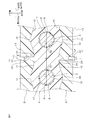
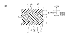
- FIG. 1 is a front sectional view of an embodiment of the inductor of the present invention.
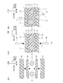
- 2A to 2C explain the method of manufacturing the inductor shown in FIG. 1,
- FIG. 2A shows the steps of preparing the first to second wirings and the first to third magnetic sheets, and
- FIG. 2B shows them.
- the process of hot pressing FIG. 2C shows the process of forming the slit and the second slit.
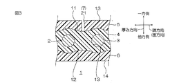
- FIG. 3 is a normal cross-sectional view of a modified example of the inductor shown in FIG. 1 (a mode not provided with a second slit).
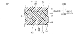
- FIG. 4 is a normal cross-sectional view of a modified example of the inductor shown in FIG.
- FIG. 5 is a normal cross-sectional view of a modified example of the inductor shown in FIG. 1 (a mode in which the slit is not exposed from the third surface and the second slit is not exposed from the fourth surface).
- FIG. 6 shows a modification of the inductor shown in FIG. 1 (a mode in which the slit does not face the first surface and is not exposed from the third surface, and the second slit does not face the second surface and is not exposed from the fourth surface. ) Is a regular cross-sectional view.
- FIG. 7 is a normal cross-sectional view of a modified example of the inductor shown in FIG.
- FIG. 8 is a normal cross-sectional view of a modified example of the inductor shown in FIG. 1 (a mode in which a slit leads to an intermediate slit and a second slit leads to a second intermediate slit).
- FIG. 9 shows a modification of the inductor shown in FIG. 1 (the slit length L2 in the thickness direction is shorter than the slit length L3 in the adjacent direction, and the second slit length L4 in the thickness direction is the second in the adjacent direction. It is a regular cross-sectional view of 2 slits (aspect shorter than length L5).
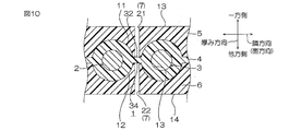
- FIG. 10 is a normal cross-sectional view of a modified example of the inductor shown in FIG. 1 (a mode in which the recess and the second recess overlap the first wiring and the second wiring when projected in the adjacent direction).
- FIG. 11 is a normal cross-sectional view of a modified example of the inductor shown in FIG. 1 (a mode in which the slit and the second slit are displaced).
- FIG. 12 is a normal cross-sectional view of a modified example of the inductor shown in FIG. 1 (a mode in which the first suppressing portion is the first filling portion and the second suppressing portion is the second filling portion).
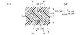
- FIG. 13 is a normal cross-sectional view of a modified example of the inductor shown in FIG.
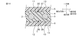
- FIG. 14 is a normal cross-sectional view of a modified example of the inductor shown in FIG. 13 (a mode in which each of the first filling portion and the second filling portion has a substantially circular shape in cross section).
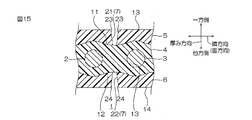
- FIG. 15 is a normal cross-sectional view of a modified example of the inductor shown in FIG. 1 (a mode in which each of the inner side surface and the second inner side surface has a tapered shape).
- 16A to 16B explain a method of manufacturing an inductor of a modified example (including a machining mode)
- FIG. 16B is a step of arranging a machining stability layer and a second machining stability layer
- FIG. 16B is a slit and a second. 2 The process of forming a slit is shown.
- FIGS. 1 to 2C An embodiment of the inductor of the present invention will be described with reference to FIGS. 1 to 2C.
- the first wiring 2 to the second wiring 3, the first magnetic sheet 25 to the third magnetic sheet 27, and the first magnetic layer 4 to the third magnetic layer 6 all of which will be described later.
- the lead wire 8 and the insulating film 9 are omitted, and the first wiring 2 and the second wiring 3 (described later) are simply drawn.
- the inductor 1 has a sheet shape extending in the plane direction.
- the inductor 1 includes a first wiring 2, a second wiring 3, a first magnetic layer 4, a second magnetic layer 5, a third magnetic layer 6, and a suppression unit 7.
- the first wiring 2 and the second wiring 3 are adjacent to each other with a gap from each other.
- the first wiring 2 and the second wiring 3 are parallel to each other.
- Each of the first wiring 2 and the second wiring 3 has a substantially circular shape when cut in a cross section (regular cross section) orthogonal to the direction of transmitting current (paper thickness direction in FIG. 1) (longitudinal direction).
- Each of the first wiring 2 and the second wiring 3 includes a lead wire 8 and an insulating film 9 for covering the lead wire 8.
- the conductor wire 8 is a conductor wire.
- the lead wire 8 has a substantially circular shape in cross section that shares the central axis with each of the first wiring 2 and the second wiring 3.
- Examples of the material of the lead wire 8 include metal conductors such as copper, silver, gold, aluminum, nickel, and alloys thereof, and copper is preferable.
- the conducting wire 8 may have a single-layer structure, or may have a multi-layer structure in which the surface of a core conductor (for example, copper) is plated (for example, nickel).
- the diameter of the lead wire 8 is, for example, 50 ⁇ m or more and 5000 ⁇ m or less.
- the insulating film 9 protects the lead wire 8 from chemicals and water, and also prevents a short circuit between the lead wire 8 and the first magnetic layer 4.
- the insulating film 9 covers the entire outer peripheral surface (circumferential surface) of the lead wire 8.
- the insulating film 9 has a substantially annular shape in cross section that shares a central axis (center) with each of the first wiring 2 and the second wiring 3.
- the insulating film 9 forms the outer peripheral surfaces 17 of the first wiring 2 and the second wiring 3, respectively.
- Examples of the material of the insulating film 9 include insulating resins such as polyvinylformal, polyester, polyesterimide, polyamide (including nylon), polyimide, polyamideimide, and polyurethane. These may be used alone or in combination of two or more.
- the insulating film 9 may be composed of a single layer or may be composed of a plurality of layers.
- the thickness of the insulating film 9 is, for example, 1 ⁇ m or more and 100 ⁇ m or less.
- the ratio of the radius of the lead wire 8 to the thickness of the insulating film 9 is, for example, 2 or more and 500 or less.
- the diameter L1 (average value of the maximum lengths) of each of the first wiring 2 and the second wiring 3 is, for example, 25 ⁇ m or more and 2000 ⁇ m or less.
- the lower limit of the interval L between the adjacent first wiring 2 and the second wiring 3 is, for example, 10, preferably 50, and the upper limit is, for example, 5,000, preferably 3,000.
- the upper limit of the ratio (L1 / L) of the diameter L1 of the first wiring 2 and the second wiring 3 to the distance L between the adjacent first wiring 2 and the second wiring 3 is, for example, 200, preferably 50. It is more preferably 30, and even more preferably 20, and the lower limit is, for example, 0.01. When the ratio (L1 / L) is equal to or less than the above upper limit, the decrease in inductance can be suppressed.
- the first magnetic layer 4, the second magnetic layer 5, and the third magnetic layer 6 work together to improve the DC superimposition characteristic of the inductor 1 while improving the inductance of the inductor 1.
- the first magnetic layer 4 has a sheet shape extending in both the longitudinal direction in which the first wiring 2 and the second wiring 3 extend and the adjacent directions in which the first wiring 2 and the second wiring 3 extend in both directions (plane direction).
- the first magnetic layer 4 has a first surface 11, a second surface 12, and an inner peripheral surface 10.
- the first surface 11 is continuous in the surface direction of the first magnetic layer 4.
- the first surface 11 has a shape (for example, a wavy shape) corresponding to the first wiring 2 and the second wiring 3.
- the first surface 11 is located on one side in the thickness direction of the first wiring 2 and the second wiring 3.
- the first surface 11 has a convex portion 31 and a concave portion 32 when it has the above-mentioned wave shape.
- the convex portion 31 is along the outer peripheral surface 17 of each of the first wiring 2 and the second wiring 3.
- the concave portion 32 is located between the two convex portions 31, and is recessed toward the other side in the thickness direction.
- the recess 32 does not overlap the first wiring 2 and the second wiring 3 when projected in the adjacent direction, and is located on one side in the thickness direction of the recess 32.
- the second surface 12 is spaced apart from the first surface 11 on the other side in the thickness direction.
- the second surface is continuous in the surface direction of the first magnetic layer 4.
- the second surface 12 has a shape (for example, a wavy shape) corresponding to the first wiring 2 and the second wiring 3.
- the second surface 12 is located on the other side in the thickness direction from the first wiring 2 and the second wiring 3.
- the second surface 12 has a second convex portion 33 and a second concave portion 34 when it has the above-mentioned wave shape.
- the second convex portion 33 is along the outer peripheral surface 17 of each of the first wiring 2 and the second wiring 3.
- the second concave portion 34 is located between the two second convex portions 33, and is recessed toward one side in the thickness direction.
- the second recess 34 does not overlap the first wiring 2 and the second wiring 3 when projected in the adjacent direction, and is located on the other side in the thickness direction.
- the inner peripheral surface 10 is located between the first surface 11 and the second surface 12.
- the inner peripheral surface 10 is formed in the middle of the first magnetic layer 4 in the thickness direction.
- the inner peripheral surface 10 contacts and covers the outer peripheral surfaces 17 of the first wiring 2 and the second wiring 3, respectively.
- the specific magnetic permeability and materials of the first magnetic layer 4 will be described in detail later.
- the second magnetic layer 5 is arranged on the first surface 11 of the first magnetic layer 4.
- the second magnetic layer 5 has a sheet shape extending in the plane direction.
- the second magnetic layer 5 has a third surface 13 and a fifth surface 15.
- the third surface 13 is arranged to face the first surface 11 on one side in the thickness direction with a gap.
- the third surface 13 forms one surface in the thickness direction of the inductor 1.
- the third surface 13 may be flat or may have a wavy shape along the first surface 11, although not shown.
- the fifth surface 15 is arranged to face the third surface 13 on the other side in the thickness direction at intervals. The fifth surface 15 comes into contact with the first surface 11.
- the relative magnetic permeability and materials of the second magnetic layer 5 will be described in detail later.
- the third magnetic layer 6 is arranged on the second surface 12 of the first magnetic layer 4.
- the third magnetic layer 6 has a sheet shape extending in the plane direction.
- the third magnetic layer 6 has a fourth surface 14 and a sixth surface 16.
- the fourth surface 14 is arranged to face the second surface 12 on the other side in the thickness direction with a gap.
- the fourth surface 14 forms the other surface of the inductor 1 in the thickness direction.
- the fourth surface 14 may be flat or may have a wavy shape along the second surface 12, although not shown.
- the relative magnetic permeability of each of the second magnetic layer 5 and the third magnetic layer 6 is higher than the relative magnetic permeability of the first magnetic layer 4. Since the relative magnetic permeability of each of the second magnetic layer 5 and the third magnetic layer 6 is higher than the specific magnetic permeability of the first magnetic layer 4, the inductor 1 is excellent in DC superimposition characteristics and can maintain a high inductance value. ..
- the relative magnetic permeability of the first magnetic layer 4, the second magnetic layer 5, and the third magnetic layer 6 are all measured at a frequency of 10 MHz. Further, the relative magnetic permeability of the first magnetic sheet 25, the second magnetic sheet 26, and the third magnetic sheet 27, which are precursors of the first magnetic layer 4, the second magnetic layer 5, and the third magnetic layer 6, is measured in advance. It can be considered that these and the relative magnetic permeability of the first magnetic layer 4, the second magnetic layer 5 and the third magnetic layer 6 are substantially the same value.
- the lower limit of the ratio R1 of the relative magnetic permeability of the second magnetic layer 5 to the relative magnetic permeability of the first magnetic layer 4 is, for example, 1.1, preferably 1.5, more preferably 2. More preferably, it is 5, especially preferably 10, most preferably 15, and the upper limit is, for example, 10,000.
- the ratio R2 of the relative magnetic permeability of the third magnetic layer 6 to the relative magnetic permeability of the first magnetic layer 4 is the same as that of R1 described above. When the ratio R1 and / or the ratio R2 is equal to or higher than the above-mentioned lower limit, the DC superimposition characteristic is further excellent.
- the first magnetic layer 4, the second magnetic layer 5, and the third magnetic layer 6 all contain magnetic particles.
- a magnetic composition containing magnetic particles and a binder can be mentioned.
- Examples of the magnetic material constituting the magnetic particles include a soft magnetic material and a hard magnetic material.
- a soft magnetic material is preferably used from the viewpoint of inductance and DC superimposition characteristics.
- the soft magnetic material examples include a single metal body containing one kind of metal element in a pure substance state, for example, one or more kinds of metal elements (first metal element) and one or more kinds of metal elements (second metal element).
- first metal element one or more kinds of metal elements
- second metal element one or more kinds of metal elements
- the single metal body examples include a single metal composed of only one kind of metal element (first metal element).
- the first metal element is appropriately selected from, for example, iron (Fe), cobalt (Co), nickel (Ni), and other metal elements that can be contained as the first metal element of the soft magnetic material. ..
- the single metal body includes, for example, a core containing only one kind of metal element and a surface layer containing an inorganic substance and / or an organic substance that modifies a part or all of the surface of the core, for example.
- examples thereof include an organic metal compound containing a first metal element and a form in which an inorganic metal compound is decomposed (thermal decomposition, etc.).
- thermal decomposition etc.
- iron powder obtained by thermally decomposing an organic iron compound (specifically, carbonyl iron) containing iron as the first metal element (sometimes referred to as carbonyl iron powder). And so on.
- the position of the layer containing the inorganic substance and / or the organic substance that modifies the portion containing only one kind of metal element is not limited to the above-mentioned surface.
- the organometallic compound or inorganic metal compound capable of obtaining a single metal body is not particularly limited, and a known or commonly used organometallic compound or inorganic metal compound capable of obtaining a soft magnetic single metal body is not particularly limited. Can be appropriately selected from.
- the alloy body is a eutectic of one or more kinds of metal elements (first metal element) and one or more kinds of metal elements (second metal element) and / or non-metal elements (carbon, nitrogen, silicon, phosphorus, etc.). It is not particularly limited as long as it is a body and can be used as an alloy body of a soft magnetic material.
- the first metal element is an essential element in the alloy body, and examples thereof include iron (Fe), cobalt (Co), and nickel (Ni). If the first metal element is Fe, the alloy body is an Fe-based alloy, and if the first metal element is Co, the alloy body is a Co-based alloy, and the first metal element is Ni. For example, the alloy body is a Ni-based alloy.
- the second metal element is an element (sub-component) secondarily contained in the alloy body, and is a metal element that is compatible (co-fused) with the first metal element.
- iron (Fe) the first. 1
- cobalt (Co) when the first metal element is other than Co
- nickel (Ni) when the first metal element is other than Ni
- Cr chromium
- Al aluminum
- Si silicon
- Cu copper
- manganese (Mn) calcium (Ca), barium (Ba), titanium (Ti), zirconium (Zr), hafnium (Hf), vanadium (V), niobium (Nb), tantalum (Ta), molybdenum (Mo), tungsten (W), ruthenium (Ru), rhodium (Rh), zinc (Zn), gallium (Ga), indium (In), germanium Examples thereof include (Ge), tin (Sn), lead (Pb), scan
- the non-metal element is an element (sub-component) secondarily contained in the alloy body, and is a non-metal element that is compatible (combined) with the first metal element.
- boron (B) and carbon examples thereof include (C), nitrogen (N), silicon (Si), phosphorus (P) and sulfur (S). These can be used alone or in combination of two or more.
- Fe-based alloys examples include magnetic stainless steel (Fe-Cr-Al-Si alloy) (including electromagnetic stainless steel), sentust (Fe-Si-Al alloy) (including super sentust), and permalloy (including supersendust).
- magnetic stainless steel Fe-Cr-Al-Si alloy
- sentust Fe-Si-Al alloy
- permalloy including supersendust
- Fe-Ni alloy Fe-Ni alloy
- Fe-Ni-Mo alloy Fe-Ni-Mo-Cu alloy
- Fe-Ni-Co alloy Fe-Cr alloy
- Fe-Cr-Al alloy Fe-Ni-Cr alloy
- Fe- Ni—Cr—Si alloy silicon copper (Fe—Cu—Si alloy)
- Fe—Si alloy Fe—Si—B (—Cu—Nb) alloy
- Fe—B—Si—Cr alloy Fe—Si—Cr -Ni alloy
- Fe-Si-Cr alloy Fe-Si-Al-Ni-Cr alloy
- Fe-Ni-Si-Co alloy Fe-N alloy, Fe-C alloy, Fe-B alloy
- Fe-P alloy Ferrites (stainless ferrites, Mn-Mg ferrites, Mn-Zn ferrites, Ni-Zn ferrites, Ni-Zn-Cu ferrites, Cu-Zn ferrites, Cu-Mg-Zn ferrites, etc. (Including soft ferrite),
- Co-based alloys which are examples of alloys, include Co-Ta-Zr and cobalt (Co) -based amorphous alloys.
- Ni-based alloys which are examples of alloys, include Ni—Cr alloys.
- the shape of the magnetic particles is not particularly limited, and a shape exhibiting anisotropy such as a substantially flat shape (plate shape) or a substantially needle shape (including a substantially spindle (football) shape), for example, a substantially spherical shape or a substantially granular shape. , Shapes showing isotropic properties such as substantially lump shapes and the like.
- the lower limit of the average value of the maximum lengths of the magnetic particles is, for example, 0.1 ⁇ m, preferably 0.5 ⁇ m, and the upper limit is, for example, 200 ⁇ m, preferably 150 ⁇ m.
- the average value of the maximum lengths of the magnetic particles can be calculated as the medium particle diameter of the magnetic particles.
- the lower limit of the volume ratio (filling rate) of the magnetic particles in the magnetic composition is, for example, 10% by volume, preferably 20% by volume, and the upper limit is, for example, 90% by volume, preferably 80% by volume. is there.
- the binder examples include a thermoplastic component such as an acrylic resin, and a thermosetting component such as an epoxy resin composition.
- Acrylic resins include, for example, carboxyl group-containing acrylic acid ester copolymers.
- the epoxy resin composition contains, for example, an epoxy resin (cresol novolac type epoxy resin or the like) as a main agent, a curing agent for epoxy resin (phenol resin or the like), and a curing accelerator for epoxy resin (imidazole compound or the like).
- thermoplastic component and the thermosetting component can be used alone or in combination, respectively, and preferably the thermoplastic component and the thermosetting component are used in combination.
- the type, shape, size, volume ratio, etc. of the magnetic particles in the magnetic composition are appropriately adjusted so that the relative magnetic permeability of the second magnetic layer 5 and the third magnetic layer 6 is higher than the relative magnetic permeability of the first magnetic layer 4. Be changed.
- the material of the first magnetic layer 4 contains substantially spherical magnetic particles
- the materials of the second magnetic layer 5 and the third magnetic layer 6 all have a substantially flat magnetic shape. It contains particles (for example, Examples 1 to 4 described later).
- each of the materials of the first magnetic layer 4, the second magnetic layer 5, and the third magnetic layer 6 contains substantially spherical magnetic particles (for example, Examples 5 to 8 described later).
- the suppression unit 7 is configured to suppress the magnetic coupling between the first wiring 2 and the second wiring 3.
- the suppression portion 7 is located between the first wiring 2 and the second wiring 3 when projected in the thickness direction. Specifically, the suppression unit 7 does not overlap with either the first wiring 2 or the second wiring 3 when projected in the thickness direction.
- the suppression unit 7 has the first point 51 closest to the second wiring 3 on the outer peripheral surface 17 of the first wiring 2 and the first wiring 2 closest to the outer peripheral surface 17 of the second wiring 3. It is located between the second point 52 and the nearest point 52.
- the suppression unit 7 includes a slit 21 as an example of the first suppression unit and a second slit 22 as an example of the second suppression unit.
- the suppressing portion 7 includes only the slit 21 and the second slit 22.
- the slit 21 is located between the first surface 11 and the third surface 13. Specifically, the restraining portion 7 is formed over the entire thickness direction of the second magnetic layer 5. Specifically, the slit 21 penetrates the second magnetic layer 5 in the thickness direction. However, although the slit 21 penetrates the second magnetic layer 5, it does not penetrate or cut out the first magnetic layer 4. The slit 21 faces the first surface 11. That is, the slit 21 exposes the corresponding first surface 11 (recessed portion 32). Further, the slit 21 is exposed from the third surface 13. In other words, the slit 21 is open toward one side in the thickness direction.
- the slit 21 is partitioned by a recess 32 on the first surface 11 of the first magnetic layer 4 and two inner side surfaces 23 of the second magnetic layer 5 that expose the slit 21.
- the distance between the two inner surfaces 23 is the same in the thickness direction, and specifically, they are parallel to each other.
- the length L2 of the slit 21 in the thickness direction is longer than the length L3 of the slit 21 in the adjacent direction.
- the ratio (L2 / L3) of the length L2 of the slit 21 in the thickness direction to the length L3 of the slit 21 in the adjacent direction exceeds 1, and specifically, the lower limit of the ratio (L2 / L3) is, for example. It is 1.5, preferably 3, more preferably 5, even more preferably 10, and the upper limit is, for example, 1,000.
- the ratio (L2 / L3) is equal to or higher than the above lower limit, crosstalk between the first wiring 2 and the second wiring 3 can be effectively suppressed.
- the upper limit of the ratio (L3 / L) of the length L3 of the slit 21 in the adjacent direction to the distance L between the adjacent first wiring 2 and the second wiring 3 is, for example, 0.95, preferably 0.9.
- the lower limit is, for example, 0.0001.
- the upper limit of the length L3 of the slit 21 in the adjacent direction is, for example, 1,000 ⁇ m, preferably 700 ⁇ m, preferably 500 ⁇ m, more preferably 300 ⁇ m, and the lower limit is, for example, 5 ⁇ m. Is.
- the second slit 22 is located between the second surface 12 and the fourth surface 14. Specifically, the restraining portion 7 is formed over the entire thickness direction of the third magnetic layer 6.
- the second slit 22 is formed in the third magnetic layer 6. Specifically, the second slit 22 penetrates the third magnetic layer 6 in the thickness direction. However, although the second slit 22 penetrates the third magnetic layer 6, it does not penetrate or cut out the first magnetic layer 4.
- the second slit 22 faces the second surface 12. That is, the second slit 22 exposes the corresponding third surface 13 (the second recess 34). Further, the second slit 22 is exposed from the fourth surface 14. In other words, the second slit 22 is open toward the other side in the thickness direction.
- the second slit 22 is partitioned by a second recess 34 on the second surface 12 and two second inner side surfaces 24 of the third magnetic layer 6 that expose the second recess 34.
- the distance between the two second inner side surfaces 24 is the same in the thickness direction, and specifically, they are parallel to each other.
- the length L4 of the second slit 22 in the thickness direction is longer than the length L5 of the second slit 22 in the adjacent direction.
- the lower limit of the ratio (L4 / L5) of the length L4 of the second slit 22 in the thickness direction to the length L5 of the second slit 22 in the adjacent direction exceeds 1, and specifically, the ratio (L4 / L5). However, for example, it is 1.5, preferably 3, more preferably 5, and even more preferably 10, and the upper limit is, for example, 1,000.
- the ratio (L4 / L5) is equal to or higher than the above-mentioned lower limit, crosstalk between the first wiring 2 and the second wiring 3 can be effectively suppressed.
- the lower limit of the ratio (L5 / L) of the length L5 of the second slit 22 in the adjacent direction to the distance L between the adjacent first wiring 2 and the second wiring 3 is, for example, 0.95, preferably 0.9.
- the upper limit is, for example, 0.0001.
- the length L5 of the second slit 22 in the adjacent direction is the same as the length L3 of the slit 21 in the adjacent direction described above.
- the thickness of the inductor 1 is the length between the third surface 13 and the fourth surface 14.
- the lower limit of the thickness of the inductor 1 is, for example, 30 ⁇ m, preferably 50 ⁇ m
- the upper limit is, for example, 10,000 ⁇ m, preferably 2,000 ⁇ m.
- the inductor 1 first, as shown in FIG. 2A, first, the first wiring 2 and the second wiring 3, two first magnetic sheets 25, one second magnetic sheet 26, and one third magnetic Prepare the sheet 27.
- the two first magnetic sheets 25 are precursor sheets for forming the first magnetic layer 4.
- the second magnetic sheet 26 is a precursor sheet for forming the second magnetic layer 5.
- the third magnetic sheet 27 is a precursor sheet for forming the third magnetic layer 6. These precursor sheets are, for example, the B stage.
- the second magnetic sheet 26, one first magnetic sheet 25, the first wiring 2 and the second wiring 3, the other first magnetic sheet 25, and the third magnetic sheet 27 are directed toward the other side in the thickness direction. Arrange in order.
- the two first magnetic sheets 25 are deformed so as to embed the first wiring 2 and the second wiring 3 to form the first magnetic layer 4.
- the second magnetic sheet 26 is deformed so as to follow the first surface 11 to become the second magnetic layer 5.
- the third magnetic sheet 27 is deformed so as to follow the second surface 12, and becomes the third magnetic layer 6.
- the precursor sheet (first magnetic sheet 25 to third magnetic sheet 27) becomes a C stage by the above-mentioned heat press. As a result, an inductor 1 having the first magnetic layer 4 to the third magnetic layer 6 without the suppression unit 7 is obtained.
- the slit 21 and the second slit 22 are formed in the second magnetic layer 5 and the third magnetic layer 6 of the inductor 1, respectively.
- a cutting device is used to form the slit 21 and the second slit 22.
- a contact type cutting device that physically contacts the second magnetic layer 5 and / or the third magnetic layer 6, such as a dicing device, for example, a second magnetic layer 5 and / or or, such as a laser device.
- a non-contact cutting device that does not physically contact the third magnetic layer 6.
- a dicing device which is an example of a contact-type cutting device, includes a support base (not shown), a dicing saw 28 arranged to face the support base (not shown), and a moving device (not shown) for moving the dicing saw 28. ..
- Examples of the dicing saw 28 include a dicing blade having a disk shape and the like.
- the inductor 1 including the suppression portion 7 having the slit 21 and the second slit 22 is manufactured.
- the relative magnetic permeability of each of the second magnetic layer 5 and the third magnetic layer 6 is higher than the relative magnetic permeability of the first magnetic layer 4, and the suppressing portion 7 is the first surface 11 and the third surface 13.
- the suppressing portion 7 is the first surface 11 and the third surface 13.
- the slit 21 since the slit 21 is exposed from the third surface 13, the slit 21 can be easily formed.
- the first suppressing portion is the slit 21
- the air having the lowest relative magnetic permeability of 1 exists in the slit 21, although the configuration is simple. Therefore, the first wiring is made by the slit 21. Crosstalk between 2 and 2nd wiring 3 can be reliably suppressed.
- the suppression portion 7 further includes a second slit 22 located between the second surface 12 and the fourth surface 14, the first wiring 2 and the second wiring 3 can be suppressed while suppressing a decrease in inductance. Crosstalk between can be suppressed.
- the second slit 22 since the second slit 22 is exposed from the fourth surface 14, the second slit 22 can be easily formed.
- the second suppression portion is the second slit 22
- the first wiring 2 and the second wiring 2 and the second are because the air having the lowest relative magnetic permeability of 1 exists in the slit 21, although the configuration is simple.
- Crosstalk between the wirings 3 can be reliably suppressed.
- the suppressing portion 7 does not have the second slit 22 (see FIG. 1), but includes only the slit 21.
- the suppressing portion 7 includes a slit 21 and a second slit 22.
- the slit 21 does not face the first surface 11 and is separated from the first surface 11 in the thickness direction.
- the second slit 22 does not face the second surface 12, and is separated from the second surface 12 in the thickness direction.
- the slit 21 faces the first surface 11 and the second slit 22 faces the second surface 12.
- the slit 21 is not exposed from the third surface 13, and one end edge of the slit 21 in the thickness direction is closed by the second magnetic layer 5.
- the second slit 22 is not exposed from the fourth surface 14, and the other end edge of the second slit 22 in the thickness direction is closed by the third magnetic layer 6.
- the slit 21 is exposed from the third surface 13 and the second slit 22 is exposed from the fourth surface 14.
- the slit 21 does not face the first surface 11 and is not exposed from the third surface 13.
- the slit 21 is located at an intermediate portion in the thickness direction of the first surface 11 and the third surface 13.
- the second slit 22 does not face the second surface 12 and is not exposed from the fourth surface 14.
- the second slit 22 is located at the intermediate portion in the thickness direction of the second surface 12 and the fourth surface 14.
- the slit 21 and the second slit 22 communicate with each other via the intermediate slit 29.
- the intermediate slit 29 is located between the first surface 11 and the second surface 12.
- the intermediate slit 29 penetrates the first magnetic layer 4 in the thickness direction.
- the inductor 1 does not have an intermediate slit 29 formed.
- the slit 21 leads to the intermediate slit 29.
- the intermediate slit 29 is cut out from the first surface 11 of the first magnetic layer 4 toward the intermediate portion in the thickness direction.
- the second slit 22 leads to the second intermediate slit 30.
- the second intermediate slit 30 is cut out from the second surface 12 of the first magnetic layer 4 toward the intermediate portion in the thickness direction.
- the second intermediate slit 30 is arranged to face the intermediate slit 29 at a distance in the thickness direction.
- the length L2 of the slit 21 in the thickness direction is shorter than the length L3 of the slit 21 in the adjacent direction.
- the lengths L2 and L3 in the slit 21 may be the same.
- the upper limit of the ratio (L2 / L3) of the length L2 of the slit 21 in the thickness direction to the length L3 of the slit 21 in the adjacent direction is, for example, 1 or less, preferably less than 1, and the ratio (L2 / L2 /).
- the lower limit of L3) is 0.01, preferably 0.05, more preferably 0.1, and even more preferably 0.2.
- the length L4 of the second slit 22 in the thickness direction is shorter than the length L5 of the second slit 22 in the adjacent direction. Further, although not shown, the lengths L4 and L5 in the second slit 22 may be the same.
- the upper limit of the ratio (L4 / L5) of the length L4 of the second slit 22 in the thickness direction to the length L5 of the second slit 22 in the adjacent direction is, for example, 1 or less, preferably less than 1.
- the lower limit of the ratio (L2 / L3) is 0.01, preferably 0.05, more preferably 0.1, and even more preferably 0.2.
- the recess 32 on the first surface 11 overlaps the first wiring 2 and the second wiring 3 when projected in the adjacent direction.
- the second recess 34 on the second surface 12 overlaps the first wiring 2 and the second wiring 3 when projected in the adjacent direction.
- the slit 21 and the second slit 22 are offset (offset) in the adjacent direction.
- the first filling portion 37 is filled in the gap 35 which is the slit 21.
- the gap 35, which is the second slit 22, is filled with the second filling portion 38.
- the first filling portion 37 is not exposed from the third surface 13 and is embedded by the second magnetic layer 5.
- the second filling portion 38 is not exposed from the fourth surface 14, and is embedded by the third magnetic layer 6.
- Each of the first filling portion 37 and the second filling portion 38 has a substantially rectangular shape in cross section.
- the relative magnetic permeability of each of the first filling portion 37 and the second filling portion 38 is lower than the specific magnetic permeability of the first magnetic layer 4.
- Examples of the materials of the first filling portion 37 and the second filling portion 38 include non-magnetic compositions that do not contain magnetic particles and contain a binder.
- the binder is exemplified by the above-mentioned magnetic composition.
- first, two first magnetic sheets 25 and the first wiring 2 and the second wiring 3 are prepared and heat-pressed, as shown in FIG. 2A.
- the first magnetic sheet 25 contains a thermosetting component
- it is C-staged by a hot press.
- the first magnetic layer 4 is formed.
- the first filling portion 37 and the second filling portion 38 which are solid at room temperature, are respectively arranged in the recess 32 of the first surface 11 and the second recess 34 of the second surface 12, and further, they are placed in the second. 2 It is sandwiched between a magnetic sheet 26 and a third magnetic sheet 27, and they are hot-pressed.
- a second magnetic layer 5 in which the first filling portion 37 is embedded and a third magnetic layer 6 in which the second filling portion 38 is embedded are formed.
- each of the first filling portion 37 and the second filling portion 38 has a substantially circular shape in cross section.
- the two inner side surfaces 23 that partition the slit 21 have a tapered shape in which the facing lengths gradually become shorter from the third surface 13 to the first surface 11.
- the two second inner side surfaces 24 that partition the second slit 22 have a tapered shape in which the facing lengths gradually become shorter from the fourth surface 14 to the second surface 12.
- the first magnetic sheet 25 can be composed of a plurality of sheets according to the thickness of the target first magnetic layer 4.
- the second magnetic sheet 26 can be composed of a plurality of sheets according to the thickness of the target second magnetic layer 5.
- the third magnetic sheet 27 can be composed of a plurality of sheets according to the thickness of the target third magnetic layer 6.
- the shapes of the first wiring 2 and the third wiring 3 are not particularly limited, and may be, for example, a rectangular cross section.
- the second magnetic layer 5 on which the slit 21 is formed in advance can be attached to the first surface 11 of the first magnetic layer 4.
- the third magnetic layer 6 on which the second slit 22 is formed in advance can also be attached to the second surface 12 of the first magnetic layer 4.
- the inductor 1 can further include a machining stabilizing layer 71 and a machining stabilizing layer 72.
- the processing stable layer 71 and the processing stable layer 72 improve the surface processability of the second magnetic layer 5 with respect to the third surface 13 and the third magnetic layer 6 with respect to the fourth surface 14, respectively.
- the processing stable layer 71 is arranged on the third surface 13 of the second magnetic layer 5.
- a slit 21 is also formed in the processing stable layer 71.
- the processing stable layer 71 is in contact with all of the third surface 13.
- the processing stable layer 71 contains a cured product of a thermosetting resin composition. That is, the material of the processing stable layer 71 contains a thermosetting resin composition.
- thermosetting resin composition contains a thermosetting resin as an essential component and particles as an optional component.
- the thermosetting resin includes a main agent, a curing agent and a curing accelerator.
- Examples of the main agent include epoxy resin, silicone resin, and the like, and preferably, epoxy resin.
- Examples of the epoxy resin include bisphenol A type epoxy resin, bisphenol F type epoxy resin, bisphenol S type epoxy resin, modified bisphenol A type epoxy resin, modified bisphenol F type epoxy resin, modified bisphenol S type epoxy resin, and biphenyl type epoxy resin.
- Bifunctional epoxy resins such as, for example, phenol novolac type epoxy resin, cresol novolac type epoxy resin, trishydroxyphenylmethane type epoxy resin, tetraphenylol ethane type epoxy resin, dicyclopentadiene type epoxy resin, and the like. Examples include functional epoxy resins. These epoxy resins can be used alone or in combination of two or more.
- a bifunctional epoxy resin is preferable, and a bisphenol A type epoxy resin is more preferable.
- the lower limit of the epoxy equivalent of the epoxy resin is, for example, 10 g / eq.
- the upper limit is, for example, 1,000 g / eq. Is.
- the curing agent if the main agent is an epoxy resin, for example, a phenol resin, an isocyanate resin, or the like can be mentioned.
- the phenol resin include polyfunctional phenol resins such as phenol novolac resin, cresol novolac resin, phenol aralkyl resin, phenol biphenylene resin, dicyclopentadiene type phenol resin, and resol resin. These can be used alone or in combination of two or more.
- Preferred examples of the phenol resin include phenol novolac resin and phenol biphenylene resin.
- the lower limit of the total number of hydroxyl groups in the phenol resin is, for example, 0.7 equivalents, preferably 0, with respect to 1 equivalent of epoxy groups in the epoxy resin.
- the upper limit is, for example, 1.5 equivalents, preferably 1.2 equivalents.
- the lower limit of the number of parts by mass of the curing agent is, for example, 1 part by mass and, for example, 50 parts by mass with respect to 100 parts by mass of the main agent.
- the curing accelerator is a catalyst (thermosetting catalyst) (preferably an epoxy resin curing accelerator) that accelerates the curing of the main agent, and is, for example, an organic phosphorus compound, for example, 2-phenyl-4-methyl-5.
- a catalyst thermosetting catalyst
- examples include imidazole compounds such as hydroxymethylimidazole (2P4MHZ).
- the lower limit of the number of parts by mass of the curing accelerator is, for example, 0.05 parts by mass with respect to 100 parts by mass of the main agent, and the upper limit is, for example, 5 parts by mass.
- Particles are an optional component in the thermosetting resin composition.
- the particles are dispersed in the thermosetting resin.
- the particles are at least one selected from the group consisting of the first particles and the second particles.
- the first particle has a substantially spherical shape.
- the lower limit of the median diameter of the first particle is, for example, 1 ⁇ m, preferably 5 ⁇ m, and the upper limit of the median diameter of the first particle is, for example, 250 ⁇ m, preferably 200 ⁇ m.
- the median diameter of the first particle is determined by a laser diffraction type particle size distribution measuring device. Further, the median diameter of the first particle can also be obtained by, for example, a binarization process by observing the cross section of the laminated sheet 1.
- the material of the first particle is not particularly limited.
- Examples of the material of the first particles include metals, inorganic compounds, organic compounds and the like, and in order to increase the coefficient of thermal expansion, metals and inorganic compounds are preferably mentioned.
- Metals are included in the thermosetting resin composition when the processing stable layer 71 functions as an inductance improving layer.
- the metals include the magnetic material exemplified in the magnetic layer 5, preferably an organic iron compound containing iron as the first metal element, and more preferably carbonyl iron.
- the inorganic compound is contained in the thermosetting resin composition when the processing stable layer 71 functions as a thermal expansion coefficient suppressing layer.
- the inorganic compound include an inorganic filler, specifically, silica, alumina and the like, and preferably silica.
- the first particle preferably, spherical silica is mentioned, and preferably, spherical carbonyl iron is mentioned.
- the second particle has a substantially flat shape.
- the substantially flat shape includes a substantially plate shape.
- the lower limit of the flatness (flatness) of the second particle is, for example, 8, preferably 15, and the upper limit is, for example, 500, preferably 450.
- the flatness of the second particle is obtained by the same calculation method as the flatness of the magnetic particles in the magnetic layer 5 described above.
- the lower limit of the median diameter of the second particle is, for example, 1 ⁇ m, preferably 5 ⁇ m, and the upper limit of the median diameter of the second particle is, for example, 250 ⁇ m, preferably 200 ⁇ m.
- the median diameter of the second particle is determined by the same method as that of the first particle.
- the lower limit of the average thickness of the second particles is, for example, 0.1 ⁇ m, preferably 0.2 ⁇ m, and the upper limit is, for example, 3.0 ⁇ m, preferably 2.5 ⁇ m.
- the material of the second particle is an inorganic compound.
- the inorganic compound include a thermally conductive compound such as boron nitride. Therefore, preferably, the inorganic compound is contained in the thermosetting resin composition when the processing stable layer 71 functions as a thermal conductivity improving layer.
- the second particle is preferably a flat boron nitride.
- the first particle and the second particle include a single type or both in the thermosetting resin composition.
- the lower limit of the number of parts by mass of the particles (first particles and / or the second particles) with respect to 100 parts by mass of the thermosetting resin is, for example, 10 parts by mass, preferably 50 parts by mass, and the upper limit is, for example, 2. It is 000 parts by mass, preferably 1,500 parts by mass.
- the lower limit of the content ratio of the particles in the cured product is, for example, 10% by mass, and the upper limit is, for example, 90% by mass.
- the lower limit of the number of parts by mass of the second particles with respect to 100 parts by mass of the first particles is, for example, 30 parts by mass
- the upper limit is For example, 300 parts by mass.
- thermosetting resin composition does not have to contain the particles.
- the lower limit of the thickness of the processing stable layer 71 is, for example, 1 ⁇ m, preferably 10 ⁇ m, and the upper limit is, for example, 1,000 ⁇ m, preferably 100 ⁇ m.
- the lower limit of the ratio of the thickness of the processing stable layer 71 to the thickness of the laminated sheet 1 is, for example, 0.001, preferably 0.005, more preferably 0.01, and the upper limit is, for example, 0. 5, preferably 0.3, more preferably 0.1.
- the materials and dimensions of the second processing stable layer 72 are the same as those of the processing stable layer 71.
- the inductor 1 In order to manufacture the inductor 1 provided with the processing stabilizing layer 71 and the second processing stabilizing layer 72, the inductor 1 without the suppressing portion 7 is manufactured as shown in FIG. 2B, and subsequently, as shown in FIG. 16A, the inductor 1 is manufactured.
- Each of the two processing stability sheets 73 is arranged (laminated) on each of the third surface 13 and the fourth surface 14.
- the processing stability sheet 73 is formed in a sheet shape from the materials of the processing stability layer 71 and the second processing stability layer 72, respectively.
- the processing stability sheet 73 preferably contains a B-stage thermosetting resin composition.
- the above-mentioned material can be prepared as a varnish by further blending a solvent with the above-mentioned thermosetting resin composition. Further, the material may be further blended with a thermoplastic resin.
- the solvent examples include alcohol compounds such as methanol, ether compounds such as dimethyl ether, and ketone compounds such as methyl ethyl ketone and cyclohexanone.
- the mixing ratio of the solvent is adjusted so that the lower limit of the mass ratio of the solid content in the varnish is, for example, 10% by mass, and the upper limit is, for example, 95% by mass.
- the varnish is applied to the surface of a release sheet (not shown) and dried to form two processing stable sheets 73.
- the two processing stabilization sheets 73 are pressed from both sides in the thickness direction.
- the two processing stability sheets 73 are attached to the third surface 13 and the fourth surface 14, respectively.
- each of the slit 21 and the second slit 22 obtains a laminated sheet 1 formed on each of the processing stabilizing layer 71 and the second magnetic layer 5 and the second processing stabilizing layer 72 and the third magnetic layer 6. ..
- the inductor 1 of the modified example includes the processing stability layer 71, the processing stability of the second magnetic layer 5 is excellent.
- the inductor 1 does not include the processing stabilizing layer 71, and is composed only of the first wiring 2, the second wiring 3, the first magnetic layer 4, the second magnetic layer 5, and the third magnetic layer 6.
- the inner end portion of the third surface 13 of the second magnetic layer 5 facing the slit 21 warps (swells) to one side in the thickness direction.
- the magnetic particles are hard to break because they are made of metals, and the shape is substantially flat, so that the magnetic particles are around the magnetic particles.
- the second magnetic layer 5 moves to one side in the thickness direction while involving the binder.
- the inductor 1 of this embodiment includes a processing stabilizing layer 71, and the processing stabilizing layer 71 is at least one type selected from the group consisting of first particles and second particles. Contains particles as an optional component.
- the processing stable layer 71 does not contain particles, the processing stable layer 71 is not deformed due to the movement of the particles described above, and therefore, the second magnetic layer 5 is formed by the cured product in the processing stable layer 71. It is possible to suppress the deformation of.
- the processing stable layer 71 contains the first particles having a substantially spherical shape, the movement of the first particles in the processing stable layer 71 is suppressed while involving the surrounding binder. Therefore, the deformation of the second magnetic layer 5 can be suppressed by the cured product in the processing stable layer 71.
- the processing stable layer 71 contains the second particles in which the material is an inorganic compound, even if it has a substantially flat shape, when the slit 21 is formed in the second magnetic layer 5, the second Since the material of the particles is a brittle inorganic compound, the second particles are easily broken. Therefore, the movement of the second particles in the processing stable layer 71 is suppressed. As a result, the deformation of the second magnetic layer 5 can be suppressed by the cured product in the processing stable layer 71.
- the inductor 1 of the modified example includes the above-mentioned processing stabilizing layer 71, the deformation of the second magnetic layer 5 can be suppressed when the slit 21 is formed in the inductor 1.
- the inductor 1 of the modified example 1 includes the second processing stabilizing layer 72 described above, the third magnetic layer 6 is deformed when the slit 22 is formed in the third magnetic layer 6 for the above reason. Can be suppressed.
- the inductor 1 may not include the second processing stabilizing layer 72 and may include only the processing stabilizing layer 71.
- the inductor 1 of the above-described modified example (preferably the inductor 1 provided with the processing stabilizing layer 71 and the second processing stabilizing layer 72) is, for example, at least one of the tests (a) to (e). Satisfy the exam.
- Permeability change rate (%)
- Permeability change rate (%)
- Permeability change rate (%)
- Permeability change rate (%)
- Permeability change rate (%)
- the upper limit of the change rate of the magnetic permeability of the sample in the test (a) is preferably 4%, more preferably 3%.
- the inductor 1 is excellent in stability of electrolytic copper plating against immersion in a copper sulfate solution.
- the upper limit of the change rate of the magnetic permeability of the sample in the test (b) is preferably 4%, more preferably 3%.
- the inductor 1 is excellent in stability against immersion of an acid active solution.
- the upper limit of the rate of change in the magnetic permeability of the sample in the test (c) is preferably 4%, more preferably 3%.
- the reduction solution Securiganto P manufactured by Atotech Japan Co., Ltd. in the test (c) contains a sulfuric acid aqueous solution and is used as a neutralizing solution (neutralizing agent or neutralizing aqueous solution). Therefore, if the test (c) is satisfied, the inductor 1 is excellent in stability against immersion in a neutralizing solution.
- the upper limit of the rate of change in the magnetic permeability of the sample in the test (d) is preferably 4%, more preferably 3%.
- the concentrate compact CP manufactured by Atotech Japan in test (d) contains a potassium permanganate solution. Therefore, if the test (d) is satisfied, the inductor 1 is excellent in the stability of desmear (cleaning) against immersion in a potassium permanganate solution.
- the upper limit of the rate of change in the magnetic permeability of the sample in the test (e) is preferably 4%, more preferably 3%.
- the Swelling Dip Securigant P manufactured by Atotech Japan in the test (e) is an aqueous solution containing glycol ethers and sodium hydroxide, and is used as a swelling solution. Therefore, if the test (e) is satisfied, the inductor 1 is excellent in stability against immersion in a swollen liquid.
- the inductor 1 is excellent in stability against immersion of a copper sulfate solution for electrolytic copper plating, an acid active solution, a neutralizing solution, a potassium permanganate solution for desmear (cleaning), and a swelling solution, and various processes using these solutions. Excellent stability against.
- Preparation Example 1 Binder by mixing 24.5 parts by mass of epoxy resin (main agent), 24.5 parts by mass of phenol resin (curing agent), 1 part by mass of imidazole compound (curing accelerator), and 50 parts by mass of acrylic resin (thermoplastic resin). was prepared.
- the first wiring 2 and the second wiring 3 were prepared.
- the diameter L1 of each of the first wiring 2 and the second wiring 3 was 260 ⁇ m.
- the first magnetic sheet 25, the second magnetic sheet 26, and the third magnetic sheet 27 were produced so as to have the types and filling rates of the magnetic particles shown in Table 1.
- the second magnetic sheet 26, one first magnetic sheet 25, the first wiring 2 and the second wiring 3, the other first magnetic sheet 25, and the third magnetic sheet 27 and 27 were arranged in order toward the other side in the thickness direction.
- the distance L between the first wiring 2 and the second wiring 3 was 240 ⁇ m.
- Example 1 As shown in FIGS. 2C and 3, a slit 21 having a length (width) L3 of 60 ⁇ m was formed on the second magnetic layer 5 of the inductor 1 of Comparative Example 1 by using a dicing saw 28.
- the inductor 1 provided with the suppression portion 7 having the slit 21 was manufactured.
- Example 2 As shown in FIGS. 1 and 2C, the inductor 1 is processed in the same manner as in the first embodiment except that the second slit 22 having a length (width) L5 of 60 ⁇ m is further formed in the third magnetic layer 6. Manufactured.
- the suppression unit 7 has a slit 21 and a second slit 22.
- Example 3 As shown in FIG. 13, instead of the slit 21 and the second slit 22, each of the first filling portion 37 and the second filling portion 38 is embedded in the second magnetic layer 5 and the third magnetic layer 6, respectively.
- An inductor 1 having a suppression portion 7 having a first filling portion 37 and a second filling portion 38 was manufactured in the same manner as in the first embodiment.
- the first filling portion 37 and the second filling portion 38 were each made of a room temperature solid polyimide resin, and the relative magnetic permeability was 1. Each of the first filling portion 37 and the second filling portion 38 had a rectangular shape in cross section even before being embedded in the second magnetic layer 5 and the third magnetic layer 6, respectively.
- Example 4 As shown in FIG. 7, the inductor 1 was manufactured in the same manner as in Example 2 except that the slit 21 and the intermediate slit 29 leading to the second slit 22 were formed in the suppressing portion 7.
- Comparative Example 2 and Examples 5 to 8 As shown in Table 2, Comparative Examples 1 and Examples 1 to 4 were used, except that spherical magnetic particles were used instead of the flat magnetic particles contained in the second magnetic sheet 26 and the third magnetic sheet 27.
- the inductors 1 of Comparative Example 2 and Examples 5 to 8 were manufactured in the same manner as in each of the above.
- ⁇ Crosstalk> The coupling coefficients of the first wiring 2 and the second wiring 3 of the inductor 1 in each embodiment were measured. In addition, as a reference, the coupling coefficients of the first wiring 2 and the second wiring 3 of the inductor 1 of Comparative Example 1 were also measured. Crosstalk was then evaluated according to the following criteria: In the measurement, an impedance analyzer (manufactured by Agilent, "4291B") was used.
- the DC superimposition characteristic was evaluated by measuring the inductance reduction rate of the inductor 1 in each embodiment.
- An impedance analyzer manufactured by Kuwagi Electronics Co., Ltd., "65120B" was used for the measurement of the inductance reduction rate.
- the inductance reduction rate was evaluated according to the following criteria. [Inductance without applying DC bias current-Inductance with DC bias current 10A applied] / [Inductance with DC bias current 10A applied] x 100 (%) [Criteria]
- ⁇ The inductance reduction rate with respect to Comparative Example 1 or Comparative Example 2 was 50% or less.
- X The inductance reduction rate with respect to Comparative Example 1 or Comparative Example 2 exceeded 50%.
- Inductors are mounted on electronic devices and the like.
Landscapes
- Engineering & Computer Science (AREA)
- Power Engineering (AREA)
- Chemical & Material Sciences (AREA)
- Composite Materials (AREA)
- Microelectronics & Electronic Packaging (AREA)
- Coils Or Transformers For Communication (AREA)
Abstract
インダクタ1は、互いに間隔を隔てて隣り合う第1配線2および第2配線3と、面方向に連続する第1面11と、第1面11に対して厚み方向に間隔が隔てられ、面方向に連続する第2面12と、第1面11および第2面12の間において、第1配線の外周面17および第2配線の外周面17に接触する内周面10とを有する第1磁性層4と、第1面11に配置される第2磁性層5と、第2面12に配置される第3磁性層6とを備える。第2磁性層5は、第1面11と厚み方向に間隔を隔てて対向配置される第3面13を有する。第2磁性層5および第3磁性層6のそれぞれの比透磁率が、第1磁性層4の比透磁率より高い。インダクタ1は、厚み方向に投影したときに、第1配線2および第2配線3の間に位置しており、第1配線2および第2配線3の磁気的結合を抑制するように構成される抑制部7をさらに備える。抑制部7が、第1面11および第3面13の間に位置するスリット21を含む。
Description
本発明は、インダクタに関する。
インダクタは、電子機器などに搭載されて、電圧変換部材などの受動素子として用いられることが知られている。
例えば、磁性体材料からなる本体部と、その本体部の内部に埋設された銅からなる内部導体とを備えるインダクタが提案されている(例えば、特許文献1参照。)。
近年、電子機器の小型化/高性能化に伴い、インダクタにおいても同様の特性が要望され、小型化しつつインダクタンスを高めるために、密な内部導体を備えるインダクタが要望されている。しかしながら、インダクタが密な内部導体を備えると、磁性体材料によって、隣り合う内部導体同士において磁気的な結合(クロストーク)が生じるという不具合を生じる。
一方、隣り合う内部導体の間隔を広げれば、上記したクロストークを抑制できるが、インダクタンスが低下するという不具合がある。
他方、インダクタには、優れた直流重畳特性も求められる。
本発明は、直流重畳特性に優れ、かつ、インダクタンスの低下を抑制できながら、隣り合う配線の間のクロストークを抑制できるインダクタを提供する。
本発明(1)は、互いに間隔を隔てて隣り合う第1配線および第2配線と、面方向に連続する第1面と、前記第1面に対して厚み方向に間隔が隔てられ、前記面方向に連続する第2面と、前記第1面および前記第2面の間に位置し、前記第1配線の外周面および前記第2配線の外周面に接触する内周面とを有する第1磁性層と、前記第1面に配置される第2磁性層と、前記第2面に配置される第3磁性層とを備え、前記第2磁性層は、前記第1面と前記厚み方向に間隔を隔てて対向配置される第3面を有し、前記第2磁性層および前記第3磁性層のそれぞれの比透磁率が、前記第1磁性層の比透磁率より高く、前記厚み方向に投影したときに、前記第1配線および前記第2配線の間に位置しており、前記第1配線および前記第2配線の磁気的結合を抑制するように構成される抑制部をさらに備え、前記抑制部が、前記第1面および前記第3面の間に位置する第1抑制部を含む、インダクタを含む。
このインダクタでは、第2磁性層および第3磁性層のそれぞれの比透磁率が、第1磁性層の比透磁率より高く、抑制部が、第1面および第3面の間に位置する第1抑制部を含む。そのため、直流重畳特性に優れ、かつ、インダクタンスの低下を抑制できながら、第1配線および第2配線の間のクロストークを抑制できる。
本発明(2)は、前記第1抑制部が、前記第1面に臨む、(1)に記載のインダクタを含む。
このインダクタでは、第1抑制部が第1面に臨むので、第1配線および第2配線の間のクロストークを有効に抑制できる。
本発明(3)は、前記第1抑制部が、前記第3面から露出する、(1)または(2)に記載のインダクタを含む。
このインダクタでは、第1抑制部が、第3面から露出するので、第1抑制部を簡易に形成できる。
本発明(4)は、前記厚み方向における前記第1抑制部の長さが、前記第1配線および前記第2配線が隣り合う隣方向における前記第1抑制部の長さより長い、(1)~(3)のいずれか一項に記載のインダクタを含む。
このインダクタでは、インダクタンスの低下を極力抑制できながら、第1配線および第2配線の間のクロストークを有効に抑制できる。
本発明(5)は、前記第1抑制部は、前記第2磁性層に形成されるスリットである、(1)~(4)のいずれか一項に記載のインダクタを含む。
このインダクタでは、第1抑制部が、スリットであるので、構成が簡易でありながら、比透磁率が最も低い空気がスリットに存在するので、第1配線および第2配線の間のクロストークを確実に抑制できる。
本発明(6)は、前記第1抑制部は、前記第2磁性層に形成される空隙に充填される第1充填部であり、前記第1充填部の比透磁率が、前記第1磁性層の比透磁率より低い、(1)~(4)のいずれか一項に記載のインダクタを含む。
このインダクタでは、第1抑制部が、第1磁性層より比透磁率が低い第1充填部であるので、かかる第1充填部によって、第1配線および第2配線の間のクロストークを確実に抑制できる。
本発明(7)は、前記第2磁性層の前記第3面に配置される加工安定層をさらに備える、(1)~(6)のいずれか一項に記載のインダクタを含む。
このインダクタは、加工安定層を備えるので、第2磁性層の加工安定性に優れる。
本発明(8)は、前記第3磁性層は、前記第2面と前記厚み方向に間隔を隔てて対向配置される第4面を有し、前記抑制部が、前記第2面および前記第4面の間に位置する第2抑制部をさらに含む、(1)~(7)のいずれか一項に記載のインダクタを含む。
このインダクタでは、抑制部が、第2面および第4面の間に位置する第2抑制部をさらに含むので、インダクタンスの低下を抑制できながら、第1配線および第2配線の間のクロストークをより一層抑制できる。
本発明(9)は、前記第2抑制部が、前記第2面に臨む、(8)に記載のインダクタを含む。
このインダクタでは、第2抑制部が第2面に臨むので、第1配線および第2配線の間のクロストークを有効に抑制できる。
本発明(10)は、前記第2抑制部が、前記第4面から露出する、(8)または(9)に記載のインダクタを含む。
このインダクタでは、第2抑制部が第4面から露出するので、第2抑制部を簡易に形成できる。
本発明(11)は、前記厚み方向における前記第2抑制部の長さが、前記第1配線および前記第2配線が隣り合う隣方向における前記第2抑制部の長さより長い、(8)~(10)のいずれか一項に記載のインダクタを含む。
このインダクタでは、インダクタンスの低下を極力抑制できながら、第1配線および第2配線の間のクロストークを有効に抑制できる。
本発明(12)は、前記第2抑制部は、前記第3磁性層に形成される第2スリットである、(8)~(11)のいずれか一項に記載のインダクタを含む。
このインダクタでは、第2抑制部が、第2スリットであるので、構成が簡易でありながら、比透磁率が最も低い空気が第2スリットに存在するので、第1配線および第2配線の間のクロストークを確実に抑制できる。
本発明(13)は、前記第2抑制部は、前記第3磁性層に形成される空隙に充填される第2充填部であり、前記第2充填部の比透磁率が、前記第1磁性層の比透磁率より低い、(8)~(11)のいずれか一項に記載のインダクタを含む。
このインダクタでは、第2抑制部が、第1磁性層より比透磁率が低い第2充填部であるので、かかる第2充填部によって、第1配線および第2配線の間のクロストークを確実に抑制できる。
本発明(14)は、前記第3磁性層の前記第4面に配置される第2加工安定層をさらに備える、(8)~(13)のいずれか一項に記載のインダクタを含む。
このインダクタは、第2加工安定性を備えるので、第3磁性層の表面加工性に優れる。
本発明のインダクタは、直流重畳特性に優れ、かつ、インダクタンスの低下を抑制できながら、第1配線および第2配線の間のクロストークを抑制できる。
本発明のインダクタの一実施形態を、図1~図2Cを参照して説明する。なお、図2A~図2Cにおいて、第1配線2~第2配線3と、第1磁性シート25~第3磁性シート27と、第1磁性層4~第3磁性層6と(いずれも後述)の相対配置を明確に示すため、導線8および絶縁膜9(後述)を省略し、単に、第1配線2および第2配線3(後述)を描画する。
図1に示すように、インダクタ1は、面方向に延びるシート形状を有する。インダクタ1は、第1配線2と、第2配線3と、第1磁性層4と、第2磁性層5と、第3磁性層6と、抑制部7とを備える。
第1配線2および第2配線3は、互いに間隔を隔てて隣り合う。第1配線2および第2配線3は、並行する。第1配線2および第2配線3のそれぞれは、電流を伝送する方向(図1における紙厚方向)(長手方向)に直交する断面(正断面)で切断したときに、略円形状を有する。第1配線2および第2配線3のそれぞれは、導線8と、それを被覆する絶縁膜9とを備える。
導線8は、導体線である。導線8は、第1配線2および第2配線3のそれぞれと中心軸線を共有する断面視略円形状を有する。導線8の材料としては、例えば、銅、銀、金、アルミニウム、ニッケル、これらの合金などの金属導体が挙げられ、好ましくは、銅が挙げられる。導線8は、単層構造であってもよく、コア導体(例えば、銅)の表面にめっき(例えば、ニッケル)などがされた複層構造であってもよい。導線8の直径は、例えば、50μm以上、5000μm以下である。
絶縁膜9は、導線8を薬品や水から保護し、また、導線8と第1磁性層4との短絡を防止する。絶縁膜9は、導線8の外周面(円周面)全面を被覆する。絶縁膜9は、第1配線2および第2配線3のそれぞれと中心軸線(中心)を共有する断面視略円環形状を有する。絶縁膜9は、第1配線2および第2配線3のそれぞれの外周面17を形成する。絶縁膜9の材料としては、例えば、ポリビニルホルマール、ポリエステル、ポリエステルイミド、ポリアミド(ナイロンを含む)、ポリイミド、ポリアミドイミド、ポリウレタンなどの絶縁性樹脂が挙げられる。これらは、1種単独で用いてもよく、2種以上併用してもよい。絶縁膜9は、単層から構成されていてもよく、複数の層から構成されていてもよい。絶縁膜9の厚みは、例えば、1μm以上、100μm以下である。絶縁膜9の厚みに対する導線8の半径の比は、例えば、2以上、500以下ある。
第1配線2および第2配線3のそれぞれの直径L1(最大長さの平均値)は、例えば、25μm以上、2000μm以下である。
隣り合う第1配線2および第2配線3の間隔Lの下限は、例えば、10、好ましくは、50であり、また、上限は、例えば、5,000、好ましくは、3,000である。隣り合う第1配線2および第2配線3の間隔Lに対する、第1配線2および第2配線3のそれぞれの直径L1の比(L1/L)の上限は、例えば、200、好ましくは、50、より好ましくは、30、さらに好ましくは、20であり、また、下限が、例えば、0.01である。比(L1/L)が上記した上限以下であれば、インダクタンスの低下を抑制できる。
第1磁性層4、第2磁性層5および第3磁性層6は、協働して、インダクタ1のインダクタンスを向上させながら、インダクタ1の直流重畳特性を向上させる。
第1磁性層4は、第1配線2および第2配線3が延びる長手方向、および、第1配線2および第2配線3が隣り合う隣方向の両方向(面方向)に延びるシート形状を有する。第1磁性層4は、第1面11と、第2面12と、内周面10とを有する。
第1面11は、第1磁性層4の面方向に連続する。第1面11は、第1配線2および第2配線3に対応する形状(例えば、波形状)を有する。第1面11は、第1配線2および第2配線3より厚み方向一方側に位置する。
詳しくは、第1面11は、上記した波形状を有する場合には、凸部31と、凹部32とを有する。凸部31は、第1配線2および第2配線3のそれぞれの外周面17に沿う。
凹部32は、2つの凸部31の間に位置しており、厚み方向他方側に向かって凹む。凹部32は、隣方向に投影したときに、第1配線2および第2配線3に重ならず、それらより厚み方向一方側に位置する。
第2面12は、第1面11に対して厚み方向に他方側に間隔が隔てられる。第2面は、第1磁性層4の面方向に連続する。第2面12は、第1配線2および第2配線3に対応する形状(例えば、波形状)を有する。第2面12は、第1配線2および第2配線3より厚み方向他方側に位置する。
詳しくは、第2面12は、上記した波形状を有する場合には、第2凸部33と、第2凹部34とを有する。第2凸部33は、第1配線2および第2配線3のそれぞれの外周面17に沿う。
第2凹部34は、2つの第2凸部33の間に位置しており、厚み方向一方側に向かって凹む。第2凹部34は、隣方向に投影したときに、第1配線2および第2配線3に重ならず、それらより厚み方向他方側に位置する。
内周面10は、第1面11および第2面12の間に位置する。内周面10は、第1磁性層4の厚み方向途中に形成されている。内周面10は、第1配線2および第2配線3のそれぞれの外周面17に接触し、これを被覆する。
第1磁性層4の比透磁率および材料等は、後で詳述する。
第2磁性層5は、第1磁性層4の第1面11に配置されている。第2磁性層5は、面方向に延びるシート形状を有する。第2磁性層5は、第3面13と、第5面15とを有する。
第3面13は、第1面11と厚み方向一方側に間隔を隔てて対向配置されている。第3面13は、インダクタ1の厚み方向一方面を形成する。第3面13は、平坦状であり、または、図示しないが、第1面11に沿う波形状を有することもできる。
第5面15は、第3面13に対して厚み方向他方側に間隔を隔てて対向配置されている。第5面15は、第1面11に接触する。
第2磁性層5の比透磁率および材料等は、後で詳述する。
第3磁性層6は、第1磁性層4の第2面12に配置されている。第3磁性層6は、面方向に延びるシート形状を有する。第3磁性層6は、第4面14と、第6面16とを有する。
第4面14は、第2面12と厚み方向他方側に間隔を隔てて対向配置されている。第4面14は、インダクタ1の厚み方向他方面を形成する。第4面14は、平坦状であり、または、図示しないが、第2面12に沿う波形状を有することもできる。
第2磁性層5および第3磁性層6のそれぞれの比透磁率は、第1磁性層4の比透磁率より高い。第2磁性層5および第3磁性層6のそれぞれの比透磁率は、第1磁性層4の比透磁率より高いので、インダクタ1は、直流重畳特性に優れ、かつ、高いインダクタンス値を維持できる。
第1磁性層4、第2磁性層5および第3磁性層6の比透磁率は、いずれも、周波数10MHzで測定される。また、第1磁性層4、第2磁性層5および第3磁性層6の前駆体である第1磁性シート25、第2磁性シート26および第3磁性シート27の比透磁率を予め測定し、これらと第1磁性層4、第2磁性層5および第3磁性層6の比透磁率とが実質的に同値であるとみなすことができる。
具体的には、第1磁性層4の比透磁率に対する第2磁性層5の比透磁率の比R1の下限は、例えば、1.1、好ましくは、1.5、より好ましくは、2、さらに好ましくは、5、とりわけ好ましくは、10、最も好ましくは、15であり、また、上限が、例えば、10,000である。第1磁性層4の比透磁率に対する第3磁性層6の比透磁率の比R2は、上記したR1と同様である。比R1および/または比R2が上記した下限以上であれば、直流重畳特性により一層優れる。
第1磁性層4、第2磁性層5および第3磁性層6は、いずれも、磁性粒子を含有する。具体的には、第1磁性層4、第2磁性層5および第3磁性層6の材料として、例えば、磁性粒子およびバインダを含有する磁性組成物などが挙げられる。
磁性粒子を構成する磁性材料としては、例えば、軟磁性体、硬磁性体が挙げられる。好ましくは、インダクタンスおよび直流重畳特性の観点から、軟磁性体が挙げられる。
軟磁性体としては、例えば、1種類の金属元素を純物質の状態で含む単一金属体、例えば、1種類以上の金属元素(第1金属元素)と、1種類以上の金属元素(第2金属元素)および/または非金属元素(炭素、窒素、ケイ素、リンなど)との共融体(混合物)である合金体が挙げられる。これらは、単独または併用することができる。
単一金属体としては、例えば、1種類の金属元素(第1金属元素)のみからなる金属単体が挙げられる。第1金属元素としては、例えば、鉄(Fe)、コバルト(Co)、ニッケル(Ni)、その他、軟磁性体の第1金属元素として含有することが可能な金属元素の中から適宜選択される。
また、単一金属体としては、例えば、1種類の金属元素のみを含むコアと、そのコアの表面の一部または全部を修飾する無機物および/または有機物を含む表面層とを含む形態、例えば、第1金属元素を含む有機金属化合物や無機金属化合物が分解(熱分解など)された形態などが挙げられる。後者の形態として、より具体的には、第1金属元素として鉄を含む有機鉄化合物(具体的には、カルボニル鉄)が熱分解された鉄粉(カルボニル鉄粉と称される場合がある)などが挙げられる。なお、1種類の金属元素のみを含む部分を修飾する無機物および/または有機物を含む層の位置は、上記のような表面に限定されない。なお、単一金属体を得ることができる有機金属化合物や無機金属化合物としては、特に制限されず、軟磁性体の単一金属体を得ることができる公知乃至慣用の有機金属化合物や無機金属化合物から適宜選択することができる。
合金体は、1種類以上の金属元素(第1金属元素)と、1種類以上の金属元素(第2金属元素)および/または非金属元素(炭素、窒素、ケイ素、リンなど)との共融体であり、軟磁性体の合金体として利用することができるものであれば特に制限されない。
第1金属元素は、合金体における必須元素であり、例えば、鉄(Fe)、コバルト(Co)、ニッケル(Ni)などが挙げられる。なお、第1金属元素がFeであれば、合金体は、Fe系合金とされ、第1金属元素がCoであれば、合金体は、Co系合金とされ、第1金属元素がNiであれば、合金体は、Ni系合金とされる。
第2金属元素は、合金体に副次的に含有される元素(副成分)であり、第1金属元素に相溶(共融)する金属元素であって、例えば、鉄(Fe)(第1金属元素がFe以外である場合)、コバルト(Co)(第1金属元素がCo以外である場合)、ニッケル(Ni)(第1金属元素Ni以外である場合)、クロム(Cr)、アルミニウム(Al)、ケイ素(Si)、銅(Cu)、銀(Ag)、マンガン(Mn)、カルシウム(Ca)、バリウム(Ba)、チタン(Ti)、ジルコニウム(Zr)、ハフニウム(Hf)、バナジウム(V)、ニオブ(Nb)、タンタル(Ta)、モリブデン(Mo)、タングステン(W)、ルテニウム(Ru)、ロジウム(Rh)、亜鉛(Zn)、ガリウム(Ga)、インジウム(In)、ゲルマニウム(Ge)、スズ(Sn)、鉛(Pb)、スカンジウム(Sc)、イットリウム(Y)、ストロンチウム(Sr)、各種希土類元素などが挙げられる。これらは、単独使用または2種以上併用することができる。
非金属元素は、合金体に副次的に含有される元素(副成分)であり、第1金属元素に相溶(共融)する非金属元素であって、例えば、ホウ素(B)、炭素(C)、窒素(N)、ケイ素(Si)、リン(P)、硫黄(S)などが挙げられる。これらは、単独使用または2種以上併用することができる。
合金体の一例であるFe系合金として、例えば、磁性ステンレス(Fe-Cr-Al-Si合金)(電磁ステンレスを含む)、センダスト(Fe-Si-Al合金)(スーパーセンダストを含む)、パーマロイ(Fe-Ni合金)、Fe-Ni-Mo合金、Fe-Ni-Mo-Cu合金、Fe-Ni-Co合金、Fe-Cr合金、Fe-Cr-Al合金、Fe-Ni-Cr合金、Fe-Ni-Cr-Si合金、ケイ素銅(Fe-Cu-Si合金)、Fe-Si合金、Fe-Si―B(-Cu-Nb)合金、Fe-B-Si-Cr合金、Fe-Si-Cr-Ni合金、Fe-Si-Cr合金、Fe-Si-Al-Ni-Cr合金、Fe-Ni-Si-Co合金、Fe-N合金、Fe-C合金、Fe-B合金、Fe-P合金、フェライト(ステンレス系フェライト、さらには、Mn-Mg系フェライト、Mn-Zn系フェライト、Ni-Zn系フェライト、Ni-Zn-Cu系フェライト、Cu-Zn系フェライト、Cu-Mg-Zn系フェライトなどのソフトフェライトを含む)、パーメンジュール(Fe-Co合金)、Fe-Co-V合金、Fe基アモルファス合金などが挙げられる。
合金体の一例であるCo系合金としては、例えば、Co-Ta-Zr、コバルト(Co)基アモルファス合金などが挙げられる。
合金体の一例であるNi系合金としては、例えば、Ni-Cr合金などが挙げられる。
磁性粒子の形状は、特に限定されず、略扁平形状(板形状)、略針形状(略紡錘(フットボール)形状を含む)などの異方性を示す形状、例えば、略球形状、略顆粒形状、略塊形状などの等方性を示す形状などが挙げられる。
磁性粒子の最大長さの平均値の下限は、例えば、0.1μm、好ましくは、0.5μmであり、また、上限は、例えば、200μm、好ましくは、150μmである。磁性粒子の最大長さの平均値は、磁性粒子の中位粒子径として算出することができる。
磁性粒子の磁性組成物における容積割合(充填率)の下限は、例えば、10容積%、好ましくは、20容積%であり、また、上限は、例えば、90容積%、好ましくは、80容積%である。
バインダとしては、例えば、アクリル樹脂などの熱可塑性成分、例えば、エポキシ樹脂組成物などの熱硬化性成分が挙げられる。アクリル樹脂は、例えば、カルボキシル基含有アクリル酸エステルコポリマーを含む。エポキシ樹脂組成物は、例えば、主剤であるエポキシ樹脂(クレゾールノボラック型エポキシ樹脂など)と、エポキシ樹脂用硬化剤(フェノール樹脂など)と、エポキシ樹脂用硬化促進剤(イミダゾール化合物など)とを含む。
バインダとしては、熱可塑性成分および熱硬化性成分をそれぞれ単独使用または併用することができ、好ましくは、熱可塑性成分および熱硬化性成分を併用する。
なお、上記した磁性組成物のより詳細な処方については、特開2014-165363号公報などに記載される。
第2磁性層5および第3磁性層6の比透磁率が第1磁性層4の比透磁率より高くなるように、磁性組成物における磁性粒子の種類、形状、大きさ、容積割合などが適宜変更される。
磁性粒子の形状を例示すれば、第1磁性層4の材料が、略球形状の磁性粒子を含み、第2磁性層5および第3磁性層6の材料が、いずれも、略扁平形状の磁性粒子を含む(例えば、後述する実施例1~実施例4)。または、第1磁性層4、第2磁性層5および第3磁性層6のいずれの材料も、略球形状の磁性粒子を含む(例えば、後述する実施例5~実施例8)。
抑制部7は、第1配線2および第2配線3の磁気的結合を抑制するように構成される。抑制部7は、厚み方向に投影したときに、第1配線2および第2配線3の間に位置する。
詳しくは、抑制部7は、厚み方向に投影したときに、第1配線2および第2配線3のいずれにも重なららない。抑制部7は、厚み方向に投影したときに、第1配線2の外周面17において第2配線3に最も近い第1点51と、第2配線3の外周面17において第1配線2に最も近い第2点52との間に位置する。
詳しくは、抑制部7は、厚み方向に投影したときに、第1配線2および第2配線3のいずれにも重なららない。抑制部7は、厚み方向に投影したときに、第1配線2の外周面17において第2配線3に最も近い第1点51と、第2配線3の外周面17において第1配線2に最も近い第2点52との間に位置する。
抑制部7は、第1抑制部の一例としてのスリット21と、第2抑制部の一例としての第2スリット22とを備える。本実施形態において、好ましくは、抑制部7は、スリット21と、第2スリット22とのみを備える。
スリット21は、第1面11および第3面13の間に位置する。詳しくは、抑制部7は、第2磁性層5の厚み方向全体にわたって形成されている。具体的には、スリット21は、第2磁性層5を厚み方向に貫通する。但し、スリット21は、第2磁性層5を貫通するが、第1磁性層4を貫通も切り欠きもしない。スリット21は、第1面11に臨む。つまり、スリット21は、対応する第1面11(の凹部32)を露出する。また、スリット21は、第3面13から露出する。言い換えれば、スリット21は、厚み方向一方側に向かって開放されている。このスリット21は、第1磁性層4の第1面11の凹部32と、それを露出する第2磁性層5の2つの内側面23とによって、仕切られている。2つの内側面23は、それらの間隔が、厚み方向にわたって同一であり、具体的には、平行する。
厚み方向におけるスリット21の長さL2は、隣方向におけるスリット21の長さL3より長い。隣方向におけるスリット21の長さL3に対する、厚み方向におけるスリット21の長さL2の比(L2/L3)は、1を越え、具体的には、比(L2/L3)の下限が、例えば、1.5、好ましくは、3、より好ましくは、5、さらに好ましくは、10であり、また、上限は、例えば、1,000である。比(L2/L3)が上記した下限以上であれば、第1配線2および第2配線3の間のクロストークを有効に抑制できる。
隣り合う第1配線2および第2配線3の間隔Lに対する、隣方向におけるスリット21の長さL3の比(L3/L)の上限は、例えば、0.95、好ましくは、0.9であり、また、下限は、例えば、0.0001である。
具体的には、隣方向におけるスリット21の長さL3の上限は、例えば、1,000μm、好ましくは、700μm、好ましくは、500μm、より好ましくは、300μmであり、また、下限は、例えば、5μmである。
第2スリット22は、第2面12および第4面14の間に位置する。詳しくは、抑制部7は、第3磁性層6の厚み方向全体にわたって形成されている。第2スリット22は、第3磁性層6に形成されている。具体的には、第2スリット22は、第3磁性層6を厚み方向に貫通する。但し、第2スリット22は、第3磁性層6を貫通するが、第1磁性層4を貫通も切り欠きもしない。第2スリット22は、第2面12に臨む。つまり、第2スリット22は、対応する第3面13(の第2凹部34)を露出する。また、第2スリット22は、第4面14から露出する。言い換えれば、第2スリット22は、厚み方向他方側に向かって開放されている。この第2スリット22は、第2面12の第2凹部34と、それを露出する第3磁性層6の2つの第2内側面24とによって、仕切られている。2つの第2内側面24は、それらの間隔が、厚み方向にわたって同一であり、具体的には、平行する。
厚み方向における第2スリット22の長さL4は、隣方向における第2スリット22の長さL5より長い。隣方向における第2スリット22の長さL5に対する、厚み方向における第2スリット22の長さL4の比(L4/L5)の下限は、1を越え、具体的には、比(L4/L5)が、例えば、1.5、好ましくは、3、より好ましくは、5、さらに好ましくは、10であり、また、上限は、例えば、1,000である。比(L4/L5)が上記した下限以上であれば、第1配線2および第2配線3の間のクロストークを有効に抑制できる。
隣り合う第1配線2および第2配線3の間隔Lに対する、隣方向における第2スリット22の長さL5の比(L5/L)の下限は、例えば、0.95、好ましくは、0.9であり、また、上限は、例えば、0.0001である。
具体的には、隣方向における第2スリット22の長さL5は、上記した隣方向におけるスリット21の長さL3と同様である。
インダクタ1の厚みは、第3面13および第4面14の間の長さである。具体的には、インダクタ1の厚みの下限は、例えば、30μm、好ましくは、50μmであり、また、上限が、例えば、10,000μm、好ましくは、2,000μmである。
インダクタ1を得るには、図2Aに示すように、まず、第1配線2および第2配線3と、2つの第1磁性シート25と、1つの第2磁性シート26と、1つの第3磁性シート27とを準備する。
2つの第1磁性シート25は、第1磁性層4を形成するための前駆体シートである。第2磁性シート26は、第2磁性層5を形成するための前駆体シートである。第3磁性シート27は、第3磁性層6を形成するための前駆体シートである。これら前駆体シートは、例えば、Bステージである。
第2磁性シート26と、一方の第1磁性シート25と、第1配線2および第2配線3と、他方の第1磁性シート25と、第3磁性シート27とを、厚み方向他方側に向かって順に配置する。
続いて、これらを、厚み方向に熱プレスする。2つの第1磁性シート25が、第1配線2および第2配線3を埋設するように変形して、第1磁性層4となる。第2磁性シート26が、第1面11に追従するように変形して、第2磁性層5となる。第3磁性シート27が、第2面12に追従するように変形し、第3磁性層6となる。なお、上記した熱プレスによって、前駆体シート(第1磁性シート25~第3磁性シート27)は、Cステージとなる。これにより、抑制部7を備えず、第1磁性層4~第3磁性層6を備えるインダクタ1を得る。
図2Cに示すように、その後、インダクタ1の第2磁性層5および第3磁性層6のそれぞれに、スリット21および第2スリット22のそれぞれを形成する。スリット21および第2スリット22を形成するには、例えば、切削装置が用いられる。
切削装置として、例えば、ダイシング装置などの、第2磁性層5および/または第3磁性層6と物理的に接触する接触式切削装置、例えば、レーザー装置などの、第2磁性層5および/または第3磁性層6と物理的に接触しない非接触式切削装置などが挙げられる。
接触式切削装置の一例であるダイシング装置は、支持台(図示せず)と、これと間隔を隔てて対向配置されるダイシングソー28と、これを移動させる移動装置(図示せず)とを備える。ダイシングソー28としては、例えば、円盤形状を有するダイシングブレードなどが挙げられる。
これにより、スリット21および第2スリット22を有する抑制部7を備えるインダクタ1が製造される。
<一実施形態の作用効果>
このインダクタ1では、第2磁性層5および第3磁性層6のそれぞれの比透磁率が、第1磁性層4の比透磁率より高く、抑制部7が、第1面11および第3面13の間に位置するスリット21を含む。そのため、直流重畳特性に優れ、かつ、インダクタンスの低下を抑制できながら、第1配線2および第2配線3の間のクロストークを抑制できる。
このインダクタ1では、第2磁性層5および第3磁性層6のそれぞれの比透磁率が、第1磁性層4の比透磁率より高く、抑制部7が、第1面11および第3面13の間に位置するスリット21を含む。そのため、直流重畳特性に優れ、かつ、インダクタンスの低下を抑制できながら、第1配線2および第2配線3の間のクロストークを抑制できる。
このインダクタ1では、スリット21が第1面11に臨むので、第1配線2および第2配線3の間のクロストークを有効に抑制できる。
このインダクタ1では、スリット21が、第3面13から露出するので、スリット21を簡易に形成できる。
このインダクタ1では、厚み方向におけるスリット21の長さL2が、隣方向におけるスリット21の長さL3より長いため、インダクタンスの低下を極力抑制できながら、第1配線2および第2配線3の間のクロストークを有効に抑制できる。
このインダクタ1では、第1抑制部が、スリット21であるので、構成が簡易でありながら、比透磁率が1と最も低い空気がスリット21に存在することから、かかるスリット21によって、第1配線2および第2配線3の間のクロストークを確実に抑制できる。
このインダクタ1では、抑制部7が、第2面12および第4面14の間に位置する第2スリット22をさらに含むので、インダクタンスの低下を抑制できながら、第1配線2および第2配線3の間のクロストークを抑制できる。
このインダクタ1では、第2スリット22が第2面12に臨むので、第1配線2および第2配線3の間のクロストークを有効に抑制できる。
このインダクタ1では、第2スリット22が、第4面14から露出するので、第2スリット22を簡易に形成できる。
このインダクタ1では、厚み方向における第2スリット22の長さL4が、隣方向における第2スリット22の長さL5より長いため、インダクタンスの低下を極力抑制できながら、第1配線2および第2配線3の間のクロストークを有効に抑制できる。
このインダクタ1では、第2抑制部が、第2スリット22であるので、構成が簡易でありながら、比透磁率が1と最も低い空気がスリット21に存在するので、第1配線2および第2配線3の間のクロストークを確実に抑制できる。
<変形例>
変形例において、一実施形態と同様の部材および工程については、同一の参照符号を付し、その詳細な説明を省略する。また、変形例は、特記する以外、一実施形態と同様の作用効果を奏することができる。さらに、一実施形態およびその変形例を適宜組み合わせることができる。
変形例において、一実施形態と同様の部材および工程については、同一の参照符号を付し、その詳細な説明を省略する。また、変形例は、特記する以外、一実施形態と同様の作用効果を奏することができる。さらに、一実施形態およびその変形例を適宜組み合わせることができる。
図3に示すように、このインダクタ1では、抑制部7が、第2スリット22(図1参照)を有さず、スリット21のみを備える。好ましくは、第1配線2および第2配線3の間のクロストークの効率的な抑制の観点から、抑制部7は、スリット21および第2スリット22を備える。
図4に示すように、スリット21は、第1面11に臨まず、第1面11と厚み方向に間隔が隔てられる。第2スリット22は、第2面12に臨まず、第2面12と厚み方向に間隔が隔てられる。好ましくは、一実施形態のように、スリット21が、第1面11に臨み、第2スリット22が、第2面12に臨む。
図5に示すように、スリット21は、第3面13から露出せず、スリット21の厚み方向一端縁が第2磁性層5によって閉塞される。第2スリット22は、第4面14から露出せず、第2スリット22の厚み方向他端縁が第3磁性層6によって閉塞される。好ましくは、一実施形態のように、スリット21が、第3面13から露出し、第2スリット22が、第4面14から露出する。
図6に示すように、スリット21は、第1面11に臨まず、第3面13から露出しない。スリット21は、第1面11および第3面13の厚み方向中間部に位置する。第2スリット22は、第2面12に臨まず、第4面14から露出しない。第2スリット22は、第2面12および第4面14の厚み方向中間部に位置する。
図7に示すように、スリット21および第2スリット22は、中間スリット29を介して互いに通じる。中間スリット29は、第1面11および第2面12の間に位置する。中間スリット29は、第1磁性層4を厚み方向に貫通する。好ましくは、一実施形態のように、インダクタ1には、中間スリット29が形成されない。
図8に示すように、スリット21は、中間スリット29に通じる。中間スリット29は、第1磁性層4の第1面11から厚み方向中間部に向かって切り欠かれている。第2スリット22は、第2中間スリット30に通じる。第2中間スリット30は、第1磁性層4の第2面12から厚み方向中間部に向かって切り欠かれている。第2中間スリット30は、中間スリット29と厚み方向に間隔を隔てて対向配置されている。
図9に示すように、厚み方向におけるスリット21の長さL2は、隣方向におけるスリット21の長さL3より短い。また、図示しないが、スリット21における長さL2およびL3が同一であってもよい。隣方向におけるスリット21の長さL3に対する、厚み方向におけるスリット21の長さL2の比(L2/L3)の上限が、例えば、1以下、好ましくは、1未満であり、また、比(L2/L3)の下限が、0.01、好ましくは、0.05、より好ましくは、0.1、さらに好ましくは、0.2である。
厚み方向における第2スリット22の長さL4は、隣方向における第2スリット22の長さL5より短い。また、図示しないが、第2スリット22における長さL4およびL5が同一であってもよい。隣方向における第2スリット22の長さL5に対する、厚み方向における第2スリット22の長さL4の比(L4/L5)の上限が、例えば、1以下、好ましくは、1未満であり、また、比(L2/L3)の下限が、0.01、好ましくは、0.05、より好ましくは、0.1、さらに好ましくは、0.2である。
図10に示すように、第1面11における凹部32は、隣方向に投影したときに、第1配線2および第2配線3に重なる。第2面12における第2凹部34は、隣方向に投影したときに、第1配線2および第2配線3に重なる。
図11に示すように、厚み方向に投影したときに、スリット21と第2スリット22とが、隣方向において、ずれている(オフセットされている)。
図12に示すように、スリット21である空隙35に、第1充填部37が充填されている。第2スリット22である空隙35に、第2充填部38が充填されている。
図13に示すように、第1充填部37は、第3面13から露出せず、第2磁性層5によって埋設される。第2充填部38は、第4面14から露出せず、第3磁性層6によって埋設される。第1充填部37および第2充填部38のそれぞれは、断面視略矩形状を有する。第1充填部37および第2充填部38のそれぞれの比透磁率は、第1磁性層4の比透磁率より、低い。
第1充填部37および第2充填部38のそれぞれの材料は、例えば、磁性粒子を含有せず、バインダを含有する非磁性組成物が挙げられる。バインダは、上記した磁性組成物で例示される。
このインダクタ1を得るには、図2Aが参照されるように、まず、2つの第1磁性シート25と、第1配線2および第2配線3とを準備し、これらを熱プレスする。第1磁性シート25が熱硬化性成分を含有する場合には、熱プレスによって、Cステージ化する。これにより、第1磁性層4を形成する。続いて、第1面11の凹部32および第2面12の第2凹部34のそれぞれに、常温固形状の第1充填部37および第2充填部38のそれぞれを配置し、さらに、それらを第2磁性シート26および第3磁性シート27で挟み、それらを熱プレスする。これによって、第1充填部37を埋設する第2磁性層5と、第2充填部38を埋設する第3磁性層6とが形成される。
図14に示すように、第1充填部37および第2充填部38のそれぞれは、断面視略円形状を有する。
図15に示すように、スリット21を区画する2つの内側面23は、第3面13から第1面11に向かって、対向長さが次第に短くなるテーパ形状を有する。第2スリット22を区画する2つの第2内側面24は、第4面14から第2面12に向かって、対向長さが次第に短くなるテーパ形状を有する。
目的とする第1磁性層4の厚みに応じて、第1磁性シート25を複数枚から構成することができる。目的とする第2磁性層5の厚みに応じて、第2磁性シート26を複数枚から構成することができる。目的とする第3磁性層6の厚みに応じて、第3磁性シート27を複数枚から構成することができる。
図示しないが、第1配線2および第3配線3の形状は、特に限定されず、例えば、断面矩形状であってもよい。
図示しないが、スリット21が予め形成された第2磁性層5を、第1磁性層4の第1面11に貼着することもできる。第2スリット22が予め形成された第3磁性層6を、第1磁性層4の第2面12に貼着することもできる。
図16Bに示すように、インダクタ1は、加工安定層71および加工安定層72をさらに備えることができる。
加工安定層71および加工安定層72は、それぞれ、第2磁性層5の第3面13、および、第3磁性層6の第4面14に対する表面加工性を向上させる。
加工安定層71は、第2磁性層5の第3面13に配置されている。加工安定層71にも、スリット21が形成されている。加工安定層71は、第3面13の全部に接触している。
加工安定層71は、熱硬化性樹脂組成物の硬化物を含む。つまり、加工安定層71の材料は、熱硬化性樹脂組成物を含む。
熱硬化性樹脂組成物は、熱硬化性樹脂を必須成分として含み、粒子を任意成分として含む。
熱硬化性樹脂としては、主剤、硬化剤および硬化促進剤を含む。
主剤としては、例えば、エポキシ樹脂、シリコーン樹脂などが挙げられ、好ましくは、エポキシ樹脂が挙げられる。エポキシ樹脂としては、例えば、ビスフェノールA型エポキシ樹脂、ビスフェノールF型エポキシ樹脂、ビスフェノールS型エポキシ樹脂、変性ビスフェノールA型エポキシ樹脂、変性ビスフェノールF型エポキシ樹脂、変性ビスフェノールS型エポキシ樹脂、ビフェニル型エポキシ樹脂などの2官能エポキシ樹脂、例えば、フェノールノボラック型エポキシ樹脂、クレゾールノボラック型エポキシ樹脂、トリスヒドロキシフェニルメタン型エポキシ樹脂、テトラフェニロールエタン型エポキシ樹脂、ジシクロペンタジエン型エポキシ樹脂などの3官能以上の多官能エポキシ樹脂などが挙げられる。これらエポキシ樹脂は、単独で使用または2種以上を併用することができる。好ましくは、2官能エポキシ樹脂が挙げられ、より好ましくは、ビスフェノールA型エポキシ樹脂が挙げられる。
エポキシ樹脂のエポキシ当量の下限は、例えば、10g/eq.であり、また、上限は、例えば、1,000g/eq.である。
硬化剤としては、主剤がエポキシ樹脂であれば、例えば、フェノール樹脂、イソシアネート樹脂などが挙げられる。フェノール樹脂としては、例えば、フェノールノボラック樹脂、クレゾールノボラック樹脂、フェノールアラルキル樹脂、フェノールビフェニレン樹脂、ジシクロペンタジエン型フェノール樹脂、レゾール樹脂などの多官能フェノール樹脂が挙げられる。これらは、単独で使用または2種以上を併用することができる。フェノール樹脂として、好ましくは、フェノールノボラック樹脂、フェノールビフェニレン樹脂が挙げられる。主剤がエポキシ樹脂であり、硬化剤がフェノール樹脂であれば、エポキシ樹脂中のエポキシ基1当量に対して、フェノール樹脂中の水酸基の合計の下限が、例えば、0.7当量、好ましくは、0.9当量、また、上限が、例えば、1.5当量、好ましくは、1.2当量である。具体的には、硬化剤の質量部数の下限は、主剤100質量部に対して、例えば、1質量部であり、また、例えば、50質量部である。
硬化促進剤としては、主剤の硬化を促進する触媒(熱硬化触媒)(好ましくは、エポキシ樹脂硬化促進剤)であって、例えば、有機リン系化合物、例えば、2-フェニル-4-メチル-5-ヒドロキシメチルイミダゾール(2P4MHZ)などのイミダゾール化合物などが挙げられる。硬化促進剤の質量部数の下限は、主剤100質量部に対して、例えば、0.05質量部であり、また、上限が、例えば、5質量部である。
粒子は、熱硬化性樹脂組成物における任意成分である。粒子は、熱硬化性樹脂に分散されている。粒子は、第1粒子、および、第2粒子からなる群から選択される少なくとも1種類である。
第1粒子は、略球形状を有する。第1粒子のメジアン径の下限は、例えば、1μm、好ましくは、5μmであり、また、第1粒子のメジアン径の上限は、例えば、250μm、好ましくは、200μmである。第1粒子のメジアン径は、レーザ回折式粒度分布測定装置で求められる。また、第1粒子のメジアン径は、例えば、積層シート1の断面観察による二値化処理によって、求めることもできる。
第1粒子の材料は、特に限定されない。第1粒子の材料としては、例えば、金属類、無機化合物、有機化合物などが挙げられ、熱膨張係数を上げるために、好ましくは、金属類、無機化合物が挙げられる。
金属類は、加工安定層71をインダンクタンス向上層として機能させる場合に熱硬化性樹脂組成物に含まれる。金属類としては、磁性層5で例示した磁性体が挙げられ、好ましくは、第1金属元素として鉄を含む有機鉄化合物、より好ましくは、カルボニル鉄が挙げられる。
無機化合物は、加工安定層71を熱膨張係数抑制層として機能させる場合に熱硬化性樹脂組成物に含まれる。無機化合物としては、例えば、無機フィラーが挙げられ、具体的には、シリカ、アルミナなどが挙げられ、好ましくは、シリカが挙げられる。
具体的には、第1粒子として、好ましくは、球形状シリカが挙げられ、また、好ましくは、球形状カルボニル鉄が挙げられる。
第2粒子は、略扁平形状を有する。略扁平形状は、略板形状を含む。
第2粒子の扁平率(扁平度)の下限は、例えば、8、好ましくは、15であり、また、上限は、例えば、500、好ましくは、450である。第2粒子の扁平率は、上記した磁性層5における磁性粒子の扁平率と同じ算出方法で求められる。
第2粒子のメジアン径の下限は、例えば、1μm、好ましくは、5μmであり、また、第2粒子のメジアン径の上限は、例えば、250μm、好ましくは、200μmである。
第2粒子のメジアン径は、第1粒子のそれと同様の方法で求められる。
第2粒子のメジアン径は、第1粒子のそれと同様の方法で求められる。
第2粒子の平均厚みの下限は、例えば、0.1μm、好ましくは、0.2μmであり、また、上限は、例えば、3.0μm、好ましくは、2.5μmである。
第2粒子の材料は、無機化合物である。無機化合物としては、例えば、窒化ホウ素などの熱伝導性化合物などが挙げられる。従って、好ましくは、無機化合物は、加工安定層71を熱伝導性向上層として機能させる場合に熱硬化性樹脂組成物に含まれる。
具体的には、第2粒子として、好ましくは、扁平形状の窒化ホウ素が挙げられる。
第1粒子および第2粒子は、熱硬化性樹脂組成物に、単独種類が含まれ、または、両方が含まれる。
熱硬化性樹脂100質量部に対する粒子(第1粒子および/または第2粒子)の質量部数の下限は、例えば、10質量部、好ましくは、50質量部であり、また、上限は、例えば、2,000質量部、好ましくは、1,500質量部である。また、硬化物における粒子の含有割合の下限は、例えば、10質量%、また、上限は、例えば、90質量%である。第1粒子および第2粒子の両方が熱硬化性樹脂組成物に含まれる場合には、第1粒子100質量部に対する第2粒子の質量部数の下限は、例えば、30質量部、また、上限は、例えば、300質量部である。
粒子は、熱硬化性樹脂組成物における任意成分であることから、熱硬化性樹脂組成物が、粒子を含有しなくてもよい。
加工安定層71の厚みの下限は、例えば、1μm、好ましくは、10μmであり、また、上限は、例えば、1,000μm、好ましくは、100μmである。積層シート1の厚みにおける加工安定層71の厚みの比の下限は、例えば、0.001、好ましくは、0.005、より好ましくは、0.01であり、また、上限は、例えば、0.5、好ましくは、0.3、より好ましくは、0.1である。
第2加工安定層72の材料および寸法は、加工安定層71のそれらと同様である。
加工安定層71および第2加工安定層72を備えるインダクタ1を製造するには、図2Bに示すように、抑制部7を備えないインダクタ1を作製し、続いて、図16Aに示すように、2つの加工安定シート73のそれぞれを、第3面13および第4面14のそれぞれに配置(積層)する。
加工安定シート73は、加工安定層71および第2加工安定層72の材料からシート形状にそれぞれ形成されている。加工安定シート73は、好ましくは、Bステージの熱硬化性樹脂組成物を含む。
なお、上記した材料を、上記した熱硬化性樹脂組成物に、溶媒をさらに配合して、ワニスとして調製することもできる。さらに、材料には、熱可塑性樹脂をさらに配合することもできる。
溶媒としては、例えば、メタノールなどのアルコール化合物、ジメチルエーテルなどのエーテル化合物、メチルエチルケトン、シクロヘキサノンなどのケトン化合物が挙げられる。溶媒の配合割合は、ワニスにおける固形分の質量割合の下限が、例えば、10質量%、また、上限が、例えば、95質量%となるように、調整される。
この方法では、ワニスを図示しない剥離シートの表面に塗布および乾燥させて、2つの加工安定シート73を形成する。
続いて、2つの加工安定シート73を、厚み方向両側からプレスする。2つの加工安定シート73を、第3面13および第4面14のそれぞれに貼付する。
その後、それらを加熱して、加工安定シート73をCステージ化する。これによって、スリット21を加工安定層71と第2磁性層5とに形成する。また、第2スリット22を、第2加工安定層72と第3磁性層6とに形成する。これによって、スリット21および第2スリット22のそれぞれが、加工安定層71および第2磁性層5と、第2加工安定層72および第3磁性層6とのそれぞれに形成された積層シート1を得る。
変形例のインダクタ1は、加工安定層71を備えるので、第2磁性層5の加工安定性に優れる。
詳述すれば、図示しないが、インダクタ1が、加工安定層71を備えず、第1配線2、第2配線3、第1磁性層4、第2磁性層5および第3磁性層6のみからなる場合には、第2磁性層5にスリット21を形成すると、第2磁性層5の第3面13におけるスリット21に臨む内端部が、厚み方向一方側に反り上がる(盛り上がる)。この事象は、スリット21を第2磁性層5に形成する時に、磁性粒子は、金属類からなることから、割れにくく、また、その形状が、略扁平形状であることから、磁性粒子の周囲のバインダを巻き込みながら、第2磁性層5が厚み方向一方側に移動する。
しかし、この一実施形態のインダクタ1は、図16Bに示すように、加工安定層71を備え、その加工安定層71が、第1粒子および第2粒子からなる群から選択される少なくとも1種類の粒子を任意成分として含有する。
具体的には、加工安定層71が粒子を含まない場合には、上記した粒子の移動に起因する加工安定層71の変形がなく、そのため、加工安定層71における硬化物によって第2磁性層5の変形を押さえ込むことができる。
加工安定層71が略球形状である第1粒子を含む場合には、周囲のバインダを巻き込みながらの、加工安定層71における第1粒子の移動が抑制される。そのため、加工安定層71における硬化物によって第2磁性層5の変形を押さえ込むことができる。
加工安定層71が、材料が無機化合物である第2粒子を含む場合には、それが、たとえ、略扁平形状であっても、スリット21を第2磁性層5に形成するときに、第2粒子の材料が脆い無機化合物であることから、第2粒子が割れ易い。そのため、加工安定層71における第2粒子の移動が抑制される。その結果、加工安定層71における硬化物によって第2磁性層5の変形を押さえ込むことができる。
従って、変形例のインダクタ1は、上記した加工安定層71を備えるので、インダクタ1にスリット21を形成するときに、第2磁性層5の変形を抑制できる。
また、この変形例1のインダクタ1は、上記した第2加工安定層72を備えるので、上記した理由により、第3磁性層6にスリット22を形成するときに、第3磁性層6の変形を抑制できる。
なお、図示しないが、インダクタ1は、第2加工安定層72を備えず、加工安定層71のみを備えることもできる。
また、上記した変形例のインダクタ1(好ましくは、加工安定層71および第2加工安定層72を備えるインダクタ1)は、例えば、試験(a)~試験(e)のうち、少なくともいずれか一つの試験を満足する。
試験(a):インダクタ1を3cm角に外形加工してサンプルを作製し、その周波数10MHzにおける比透磁率μ1を求める。その後、サンプルを、硫酸銅5水和物66g/L、硫酸濃度180g/L、塩素50ppm、トップルチナを含有する硫酸銅めっき溶液200mLに、25℃で、120分浸漬し、その後、サンプルの周波数10MHzにおける比透磁率μ2を求める。下記式によって、浸漬前後における透磁率の変化率を求める。
その結果、サンプルの透磁率の変化率が5%以下である。
その結果、サンプルの透磁率の変化率が5%以下である。
透磁率の変化率(%)=|μ1-μ2|/μ1×100
試験(b):インダクタ1を3cm角に外形加工してサンプルを作製し、その周波数10MHzにおける比透磁率μ3を求める。その後、サンプルを、硫酸55g/Lを含有する酸活性水溶液200mLに、25℃で、1分浸漬し、その後、サンプルの周波数10MHzにおける比透磁率μ4を求める。下記式によって、浸漬前後における透磁率の変化率を求める。その結果、サンプルの透磁率の変化率が5%以下である。
試験(b):インダクタ1を3cm角に外形加工してサンプルを作製し、その周波数10MHzにおける比透磁率μ3を求める。その後、サンプルを、硫酸55g/Lを含有する酸活性水溶液200mLに、25℃で、1分浸漬し、その後、サンプルの周波数10MHzにおける比透磁率μ4を求める。下記式によって、浸漬前後における透磁率の変化率を求める。その結果、サンプルの透磁率の変化率が5%以下である。
透磁率の変化率(%)=|μ3-μ4|/μ3×100
試験(c):インダクタ1を3cm角に外形加工してサンプルを作製し、その周波数10MHzにおける比透磁率μ5を求める。その後、サンプルを、アトテックジャパン社製のリダクションソリューション セキュリガントP 200mLに、45℃で、5分浸漬し、その後、サンプルの周波数10MHzにおける比透磁率μ6を求める。下記式によって、浸漬前後における透磁率の変化率を求める。その結果、サンプルの透磁率の変化率が5%以下である。
試験(c):インダクタ1を3cm角に外形加工してサンプルを作製し、その周波数10MHzにおける比透磁率μ5を求める。その後、サンプルを、アトテックジャパン社製のリダクションソリューション セキュリガントP 200mLに、45℃で、5分浸漬し、その後、サンプルの周波数10MHzにおける比透磁率μ6を求める。下記式によって、浸漬前後における透磁率の変化率を求める。その結果、サンプルの透磁率の変化率が5%以下である。
透磁率の変化率(%)=|μ5-μ6|/μ5×100
試験(d):インダクタ1を3cm角に外形加工してサンプルを作製し、その周波数10MHzにおける比透磁率μ7を求める。その後、サンプルを、アトテックジャパン社製のコンセントレート・コンパクトCP 200mLに、80℃で、15分浸漬し、その後、サンプルの周波数10MHzにおける比透磁率μ8を求める。下記式によって、浸漬前後における透磁率の変化率を求める。その結果、サンプルの透磁率の変化率が5%以下である。
試験(d):インダクタ1を3cm角に外形加工してサンプルを作製し、その周波数10MHzにおける比透磁率μ7を求める。その後、サンプルを、アトテックジャパン社製のコンセントレート・コンパクトCP 200mLに、80℃で、15分浸漬し、その後、サンプルの周波数10MHzにおける比透磁率μ8を求める。下記式によって、浸漬前後における透磁率の変化率を求める。その結果、サンプルの透磁率の変化率が5%以下である。
透磁率の変化率(%)=|μ7-μ8|/μ7×100
試験(e):インダクタ1を3cm角に外形加工してサンプルを作製し、その周波数10MHzにおける比透磁率μ9を求める。その後、サンプルを、アトテックジャパン社製のスウェリングディップ・セキュリガントP 200mLに、60℃で、5分浸漬し、その後、サンプルの周波数10MHzにおける比透磁率μ10を求める。下記式によって、浸漬前後における透磁率の変化率を求める。その結果、サンプルの透磁率の変化率が5%以下である。
試験(e):インダクタ1を3cm角に外形加工してサンプルを作製し、その周波数10MHzにおける比透磁率μ9を求める。その後、サンプルを、アトテックジャパン社製のスウェリングディップ・セキュリガントP 200mLに、60℃で、5分浸漬し、その後、サンプルの周波数10MHzにおける比透磁率μ10を求める。下記式によって、浸漬前後における透磁率の変化率を求める。その結果、サンプルの透磁率の変化率が5%以下である。
透磁率の変化率(%)=|μ9-μ10|/μ9×100
試験(a)を満足する場合において、試験(a)におけるサンプルの透磁率の変化率の上限は、好ましくは、4%、より好ましくは、3%である。
試験(a)を満足する場合において、試験(a)におけるサンプルの透磁率の変化率の上限は、好ましくは、4%、より好ましくは、3%である。
試験(a)を満足すれば、インダクタ1は、電解銅めっきの硫酸銅溶液の浸漬に対する安定性に優れる。
試験(b)を満足する場合において、試験(b)におけるサンプルの透磁率の変化率の上限は、好ましくは、4%、より好ましくは、3%である。
試験(b)を満足すれば、インダクタ1は、酸活性溶液の浸漬に対する安定性に優れる。
試験(c)を満足する場合において、試験(c)におけるサンプルの透磁率の変化率の上限は、好ましくは、4%、より好ましくは、3%である。
試験(c)におけるアトテックジャパン社製のリダクションソリューション セキュリガントPは、硫酸水溶液を含有しており、中和液(中和剤、または、中和用水溶液)として用いられる。従って、試験(c)を満足すれば、インダクタ1は、中和液浸漬に対する安定性に優れる。
試験(d)を満足する場合において、試験(d)におけるサンプルの透磁率の変化率の上限は、好ましくは、4%、より好ましくは、3%である。
試験(d)におけるアトテックジャパン社製のコンセントレート・コンパクトCPは、過マンガン酸カリウム溶液を含有する。従って、試験(d)を満足すれば、インダクタ1は、デスミア(洗浄)の過マンガン酸カリウム溶液浸漬に対する安定性に優れる。
試験(e)を満足する場合において、試験(e)におけるサンプルの透磁率の変化率の上限は、好ましくは、4%、より好ましくは、3%である。
試験(e)におけるアトテックジャパン社製のスウェリングディップ・セキュリガントPは、グリコールエーテル類および水酸化ナトリウムを含有する水溶液であって、膨潤液として用いられる。従って、試験(e)を満足すれば、インダクタ1は、膨潤液浸漬に対する安定性に優れる。
好ましくは、試験(a)~試験(e)のいずれをも満足する。そのため、インダクタ1は、電解銅めっきの硫酸銅溶液、酸活性溶液、中和液、デスミア(洗浄)の過マンガン酸カリウム溶液および膨潤液の浸漬に対する安定性に優れ、これらの液を用いる各種プロセスに対する安定性に優れる。
以下に調製例、実施例および比較例を示し、本発明をさらに具体的に説明する。なお、本発明は、何ら調製例、実施例および比較例に限定されない。また、以下の記載において用いられる配合割合(含有割合)、物性値、パラメータなどの具体的数値は、上記の「発明を実施するための形態」において記載されている、それらに対応する配合割合(含有割合)、物性値、パラメータなど該当記載の上限(「以下」、「未満」として定義されている数値)または下限(「以上」、「超過」として定義されている数値)に代替することができる。
調製例1
(バインダーの調製)
エポキシ樹脂(主剤)24.5質量部、フェノール樹脂(硬化剤)24.5質量部、イミダゾール化合物(硬化促進剤)1質量部、アクリル樹脂(熱可塑性樹脂)50質量部を混合して、バインダーを調製した。
(バインダーの調製)
エポキシ樹脂(主剤)24.5質量部、フェノール樹脂(硬化剤)24.5質量部、イミダゾール化合物(硬化促進剤)1質量部、アクリル樹脂(熱可塑性樹脂)50質量部を混合して、バインダーを調製した。
比較例1
まず、第1配線2および第2配線3を準備した。第1配線2および第2配線3のそれぞれの直径L1は、260μmであった。併せて、第1磁性シート25、第2磁性シート26および第3磁性シート27を、表1に記載の磁性粒子の種類、充填率となるように、作製した。
まず、第1配線2および第2配線3を準備した。第1配線2および第2配線3のそれぞれの直径L1は、260μmであった。併せて、第1磁性シート25、第2磁性シート26および第3磁性シート27を、表1に記載の磁性粒子の種類、充填率となるように、作製した。
図2Aに示すように、続いて、第2磁性シート26と、一方の第1磁性シート25と、第1配線2および第2配線3と、他方の第1磁性シート25と、第3磁性シート27とを、厚み方向他方側に向かって順に配置した。なお、第1配線2および第2配線3の間隔Lは、240μmであった。
図2Bに示すように、続いて、これらを熱プレスし、これにより、第1磁性層4、第2磁性層5および第3磁性層6を形成した。これにより、抑制部7を備えないインダクタ1を製造した。
実施例1
図2Cおよび図3に示すように、比較例1のインダクタ1の第2磁性層5に、ダイシングソー28を用いて、長さ(幅)L3が60μmであるスリット21を形成した。
図2Cおよび図3に示すように、比較例1のインダクタ1の第2磁性層5に、ダイシングソー28を用いて、長さ(幅)L3が60μmであるスリット21を形成した。
これによって、スリット21を有する抑制部7を備えるインダクタ1を製造した。
実施例2
図1および図2Cに示すように、第3磁性層6に、長さ(幅)L5が60μmである第2スリット22をさらに形成した以外は、実施例1と同様に処理して、インダクタ1を製造した。なお、抑制部7は、スリット21および第2スリット22を有する。
図1および図2Cに示すように、第3磁性層6に、長さ(幅)L5が60μmである第2スリット22をさらに形成した以外は、実施例1と同様に処理して、インダクタ1を製造した。なお、抑制部7は、スリット21および第2スリット22を有する。
実施例3
図13に示すように、スリット21および第2スリット22のそれぞれに代えて、第1充填部37および第2充填部38のそれぞれを、第2磁性層5および第3磁性層6のそれぞれに埋設した以外は、実施例1と同様にして、第1充填部37および第2充填部38を有する抑制部7を備えるインダクタ1を製造した。
図13に示すように、スリット21および第2スリット22のそれぞれに代えて、第1充填部37および第2充填部38のそれぞれを、第2磁性層5および第3磁性層6のそれぞれに埋設した以外は、実施例1と同様にして、第1充填部37および第2充填部38を有する抑制部7を備えるインダクタ1を製造した。
第1充填部37および第2充填部38は、それぞれ、常温固形状ポリイミド樹脂からなり、比透磁率は、1であった。第1充填部37および第2充填部38のそれぞれは、第2磁性層5および第3磁性層6のそれぞれに埋設される前から、断面視矩形状を有していた。
実施例4
図7に示すように、抑制部7に、スリット21および第2スリット22に通じる中間スリット29を形成した以外は、実施例2と同様に処理して、インダクタ1を製造した。
図7に示すように、抑制部7に、スリット21および第2スリット22に通じる中間スリット29を形成した以外は、実施例2と同様に処理して、インダクタ1を製造した。
比較例2および実施例5~8
第2磁性シート26および第3磁性シート27に含まれる扁平形状の磁性粒子に代えて、球形状の磁性粒子を用いた以外は、表2に示すように、比較例1および実施例1~4のそれぞれと同様に処理して、比較例2および実施例5~8のそれぞれのインダクタ1を製造した。
第2磁性シート26および第3磁性シート27に含まれる扁平形状の磁性粒子に代えて、球形状の磁性粒子を用いた以外は、表2に示すように、比較例1および実施例1~4のそれぞれと同様に処理して、比較例2および実施例5~8のそれぞれのインダクタ1を製造した。
<評価>
下記の事項を評価し、それらの結果を表3~表4に記載する。
下記の事項を評価し、それらの結果を表3~表4に記載する。
<クロストーク>
各実施例におけるインダクタ1の第1配線2および第2配線3の結合係数を測定した。また、参照として、比較例1のインダクタ1の第1配線2および第2配線3の結合係数も測定した。次いで、以下の基準に従って、クロストークを評価した。なお、測定では、インピーダンスアナライザ(Agilent社製、「4291B」)を用いた。
各実施例におけるインダクタ1の第1配線2および第2配線3の結合係数を測定した。また、参照として、比較例1のインダクタ1の第1配線2および第2配線3の結合係数も測定した。次いで、以下の基準に従って、クロストークを評価した。なお、測定では、インピーダンスアナライザ(Agilent社製、「4291B」)を用いた。
[基準]
◎:比較例1または比較例2と比較して結合係数が40%以上低下した。
○:比較例1または比較例2と比較して結合係数が20%以上、40%未満低下した。
◎:比較例1または比較例2と比較して結合係数が40%以上低下した。
○:比較例1または比較例2と比較して結合係数が20%以上、40%未満低下した。
<インダクタンス>
各実施例におけるインダクタ1の第1配線2および第2配線3の相互インダクタンスを測定した。以下の基準に従って、インダクタンスを評価した。なお、測定では、インピーダンスアナライザ(Agilent社製、「4291B」)を用いた。
[基準]
○:比較例1または比較例2と比較して自己インダクタンスを70%以上維持した。
△:比較例1または比較例2と比較して自己インダクタンスを50%以上、70%未満維持した。
各実施例におけるインダクタ1の第1配線2および第2配線3の相互インダクタンスを測定した。以下の基準に従って、インダクタンスを評価した。なお、測定では、インピーダンスアナライザ(Agilent社製、「4291B」)を用いた。
[基準]
○:比較例1または比較例2と比較して自己インダクタンスを70%以上維持した。
△:比較例1または比較例2と比較して自己インダクタンスを50%以上、70%未満維持した。
<直流重畳特性>
各実施例におけるインダクタ1のインダクタンス低下率を測定して、直流重畳特性を評価した。なお、インダクタンス低下率の測定では、インピーダンスアナライザ(桑木エレクトロニクス社製、「65120B」)を用いた。以下の基準に従って、インダクタンス低下率を評価した。
[DCバイアス電流を印加しない状態でのインダクタンス-DCバイアス電流10Aを印加した状態でのインダクタンス]/[DCバイアス電流10Aを印加した状態でのインダクタンス]×100(%)
[基準]
○:比較例1または比較例2に対するインダクタンス低下率が、50%以下であった。
×:比較例1または比較例2に対するインダクタンス低下率が、50%超過であった。
各実施例におけるインダクタ1のインダクタンス低下率を測定して、直流重畳特性を評価した。なお、インダクタンス低下率の測定では、インピーダンスアナライザ(桑木エレクトロニクス社製、「65120B」)を用いた。以下の基準に従って、インダクタンス低下率を評価した。
[DCバイアス電流を印加しない状態でのインダクタンス-DCバイアス電流10Aを印加した状態でのインダクタンス]/[DCバイアス電流10Aを印加した状態でのインダクタンス]×100(%)
[基準]
○:比較例1または比較例2に対するインダクタンス低下率が、50%以下であった。
×:比較例1または比較例2に対するインダクタンス低下率が、50%超過であった。
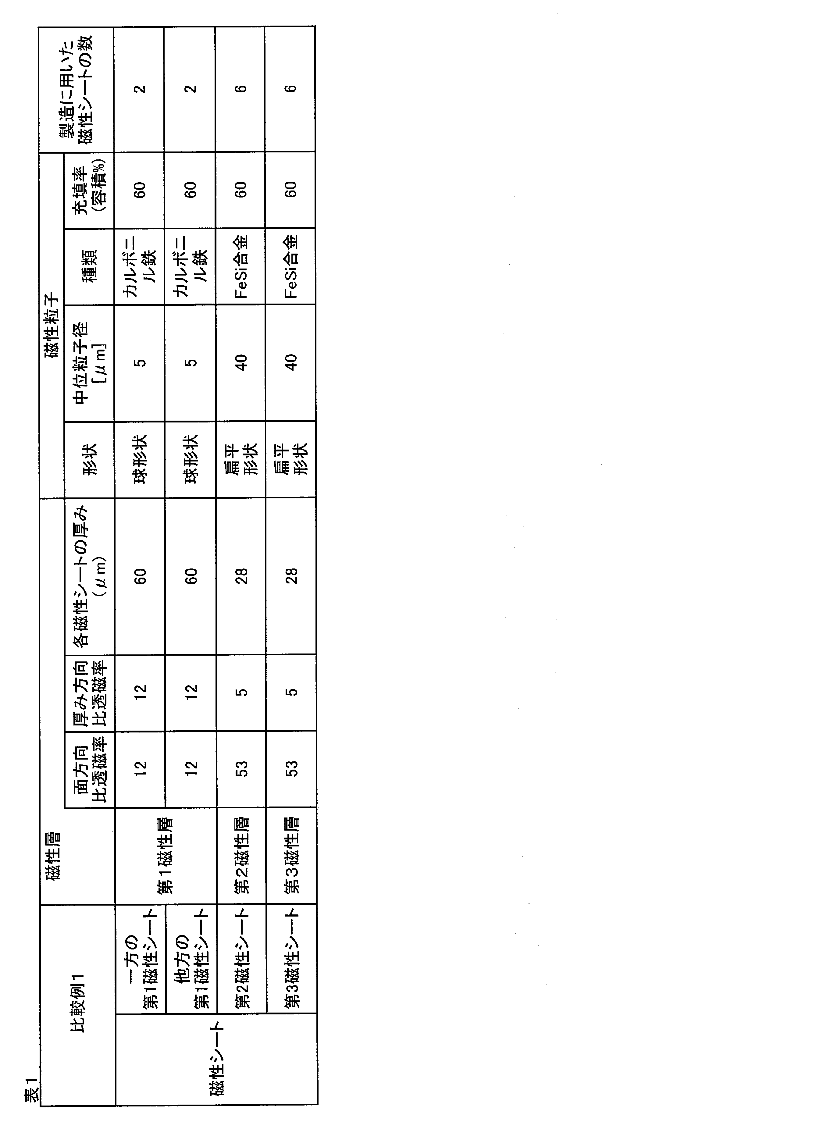
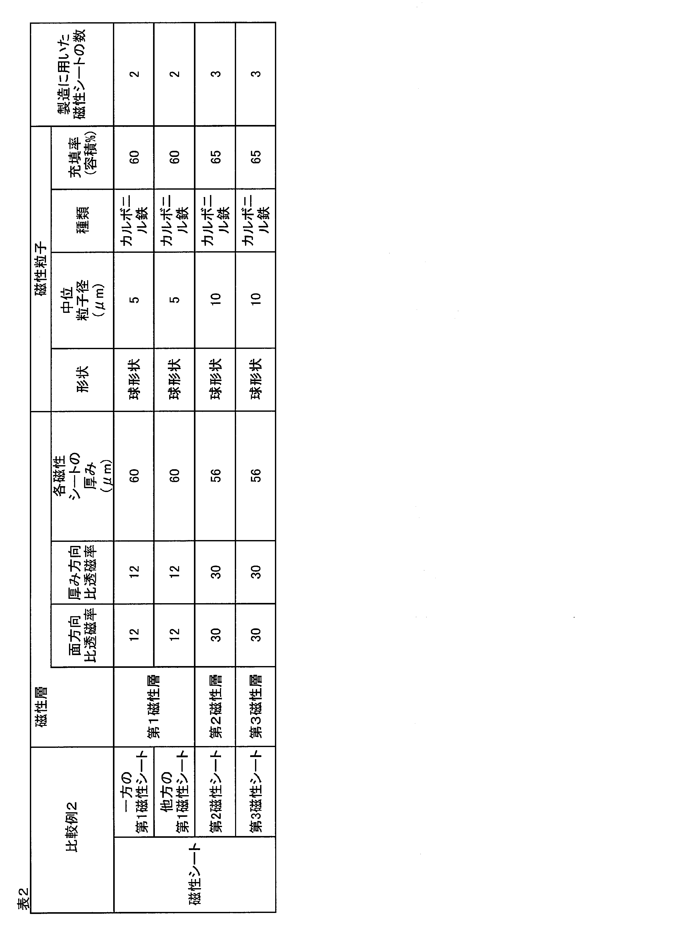
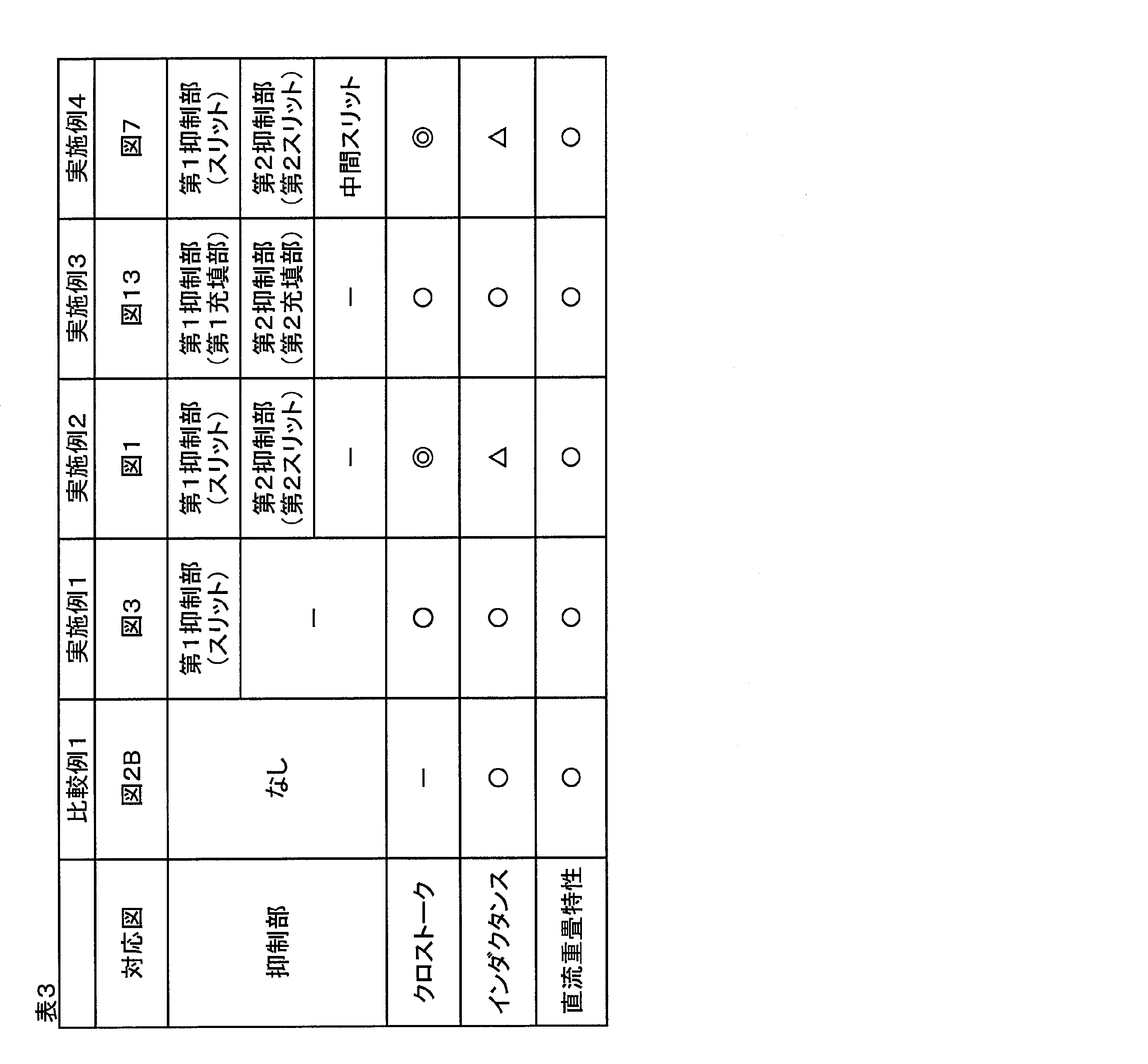
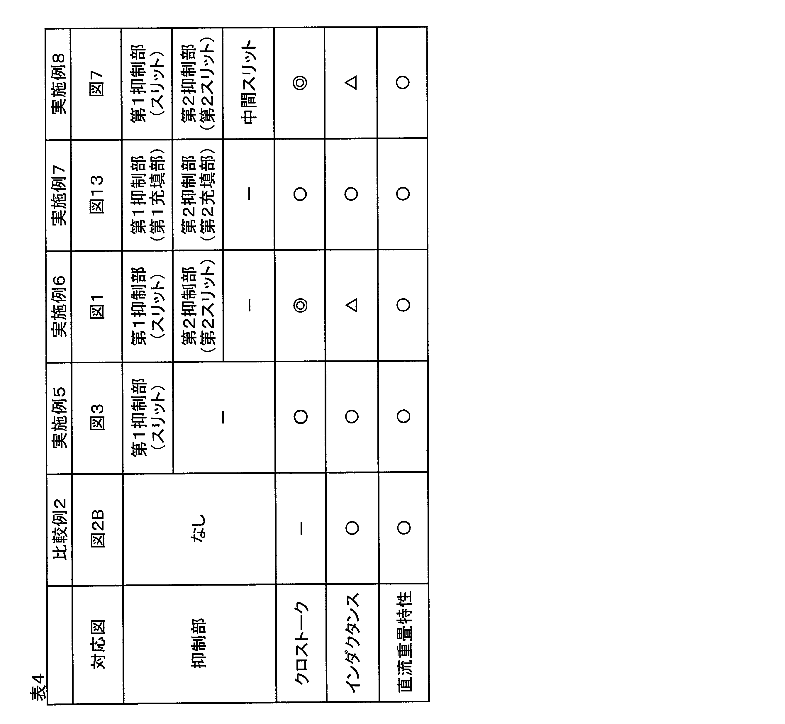
なお、上記発明は、本発明の例示の実施形態として提供したが、これは単なる例示に過ぎず、限定的に解釈してはならない。当該技術分野の当業者によって明らかな本発明の変形例は、後記請求の範囲に含まれる。
インダクタは、電子機器などに搭載される。
1 インダクタ
2 第1配線
3 第2配線
4 第1磁性層
5 第2磁性層
6 第3磁性層
7 抑制部
10 内周面
11 第1面
12 第2面
13 第3面
14 第4面
17 外周面
21 スリット
22 第2スリット
35 空隙
37 第1充填部
38 第2充填部
71 加工安定層
72 第2加工安定層
L2 厚み方向におけるスリットの長さ
L3 隣方向におけるスリットの長さ
L4 厚み方向における第2スリットの長さ
L5 隣方向における第2スリットの長さ
2 第1配線
3 第2配線
4 第1磁性層
5 第2磁性層
6 第3磁性層
7 抑制部
10 内周面
11 第1面
12 第2面
13 第3面
14 第4面
17 外周面
21 スリット
22 第2スリット
35 空隙
37 第1充填部
38 第2充填部
71 加工安定層
72 第2加工安定層
L2 厚み方向におけるスリットの長さ
L3 隣方向におけるスリットの長さ
L4 厚み方向における第2スリットの長さ
L5 隣方向における第2スリットの長さ
Claims (14)
- 互いに間隔を隔てて隣り合う第1配線および第2配線と、
面方向に連続する第1面と、前記第1面に対して厚み方向に間隔が隔てられ、前記面方向に連続する第2面と、前記第1面および前記第2面の間に位置し、前記第1配線の外周面および前記第2配線の外周面に接触する内周面とを有する第1磁性層と、
前記第1面に配置される第2磁性層と、
前記第2面に配置される第3磁性層とを備え、
前記第2磁性層は、前記第1面と前記厚み方向に間隔を隔てて対向配置される第3面を有し、
前記第2磁性層および前記第3磁性層のそれぞれの比透磁率が、前記第1磁性層の比透磁率より高く、
前記厚み方向に投影したときに、前記第1配線および前記第2配線の間に位置しており、前記第1配線および前記第2配線の磁気的結合を抑制するように構成される抑制部をさらに備え、
前記抑制部が、前記第1面および前記第3面の間に位置する第1抑制部を含むことを特徴とする、インダクタ。 - 前記第1抑制部が、前記第1面に臨むことを特徴とする、請求項1に記載のインダクタ。
- 前記第1抑制部が、前記第3面から露出することを特徴とする、請求項1に記載のインダクタ。
- 前記厚み方向における前記第1抑制部の長さが、前記第1配線および前記第2配線が隣り合う隣方向における前記第1抑制部の長さより長いことを特徴とする、請求項1に記載のインダクタ。
- 前記第1抑制部は、前記第2磁性層に形成されるスリットであることを特徴とする、請求項1に記載のインダクタ。
- 前記第1抑制部は、前記第2磁性層に形成される空隙に充填される第1充填部であり、
前記第1充填部の比透磁率が、前記第1磁性層の比透磁率より低いことを特徴とする、
請求項1に記載のインダクタ。 - 前記第2磁性層の前記第3面に配置される加工安定層をさらに備えることを特徴とする、請求項1に記載のインダクタ。
- 前記第3磁性層は、前記第2面と前記厚み方向に間隔を隔てて対向配置される第4面を有し、
前記抑制部が、前記第2面および前記第4面の間に位置する第2抑制部をさらに含むことを特徴とする、請求項1に記載のインダクタ。 - 前記第2抑制部が、前記第2面に臨むことを特徴とする、請求項8に記載のインダクタ。
- 前記第2抑制部が、前記第4面から露出することを特徴とする、請求項8に記載のインダクタ。
- 前記厚み方向における前記第2抑制部の長さが、前記第1配線および前記第2配線が隣り合う隣方向における前記第2抑制部の長さより長いことを特徴とする、請求項8に記載のインダクタ。
- 前記第2抑制部は、前記第3磁性層に形成される第2スリットであることを特徴とする、請求項8に記載のインダクタ。
- 前記第2抑制部は、前記第3磁性層に形成される空隙に充填される第2充填部であり、
前記第2充填部の比透磁率が、前記第1磁性層の比透磁率より低いことを特徴とする、
請求項8に記載のインダクタ。 - 前記第3磁性層の前記第4面に配置される第2加工安定層をさらに備えることを特徴とする、請求項8に記載のインダクタ。
Priority Applications (4)
| Application Number | Priority Date | Filing Date | Title |
|---|---|---|---|
| CN202080056567.4A CN114223043B (zh) | 2019-08-09 | 2020-06-19 | 电感器 |
| KR1020227003485A KR102893911B1 (ko) | 2019-08-09 | 2020-06-19 | 인덕터 |
| EP20851819.1A EP4012731A4 (en) | 2019-08-09 | 2020-06-19 | INDUCTOR |
| US17/633,443 US12573540B2 (en) | 2019-08-09 | 2020-06-19 | Inductor |
Applications Claiming Priority (4)
| Application Number | Priority Date | Filing Date | Title |
|---|---|---|---|
| JP2019147348 | 2019-08-09 | ||
| JP2019-147348 | 2019-08-09 | ||
| JP2020-024310 | 2020-02-17 | ||
| JP2020024310A JP7747430B2 (ja) | 2019-08-09 | 2020-02-17 | インダクタ |
Publications (1)
| Publication Number | Publication Date |
|---|---|
| WO2021029142A1 true WO2021029142A1 (ja) | 2021-02-18 |
Family
ID=74571012
Family Applications (1)
| Application Number | Title | Priority Date | Filing Date |
|---|---|---|---|
| PCT/JP2020/024103 Ceased WO2021029142A1 (ja) | 2019-08-09 | 2020-06-19 | インダクタ |
Country Status (6)
| Country | Link |
|---|---|
| US (1) | US12573540B2 (ja) |
| EP (1) | EP4012731A4 (ja) |
| JP (1) | JP2025061350A (ja) |
| KR (1) | KR102893911B1 (ja) |
| CN (1) | CN114223043B (ja) |
| WO (1) | WO2021029142A1 (ja) |
Cited By (1)
| Publication number | Priority date | Publication date | Assignee | Title |
|---|---|---|---|---|
| WO2025192160A1 (ja) * | 2024-03-11 | 2025-09-18 | 日東電工株式会社 | インダクタ |
Citations (8)
| Publication number | Priority date | Publication date | Assignee | Title |
|---|---|---|---|---|
| JPS59144107A (ja) * | 1983-02-07 | 1984-08-18 | Hitachi Metals Ltd | インダクタンス導線 |
| JPS62169407A (ja) * | 1986-01-22 | 1987-07-25 | Matsushita Electric Works Ltd | インダクンス素子 |
| JPH01146424U (ja) * | 1988-03-31 | 1989-10-09 | ||
| JPH05152130A (ja) * | 1991-11-26 | 1993-06-18 | Matsushita Electric Ind Co Ltd | 複合インダクタおよびその製造方法 |
| JPH10144526A (ja) | 1996-11-05 | 1998-05-29 | Murata Mfg Co Ltd | 積層チップインダクタ |
| JP2008288370A (ja) * | 2007-05-17 | 2008-11-27 | Nec Tokin Corp | 面実装インダクタおよびその製造方法 |
| JP2013543635A (ja) * | 2010-09-23 | 2013-12-05 | スリーエム イノベイティブ プロパティズ カンパニー | 遮蔽された電気ケーブル |
| JP2014165363A (ja) | 2013-02-26 | 2014-09-08 | Nitto Denko Corp | 軟磁性熱硬化性接着フィルム、軟磁性フィルム積層回路基板、および、位置検出装置 |
Family Cites Families (24)
| Publication number | Priority date | Publication date | Assignee | Title |
|---|---|---|---|---|
| JPS617013U (ja) | 1984-06-16 | 1986-01-16 | 富士電気化学株式会社 | インダクタ・モジユ−ル |
| JPH10270256A (ja) | 1997-03-21 | 1998-10-09 | Taiyo Yuden Co Ltd | 電子部品 |
| JP3752848B2 (ja) | 1998-05-12 | 2006-03-08 | 株式会社村田製作所 | インダクタ |
| US6392525B1 (en) * | 1998-12-28 | 2002-05-21 | Matsushita Electric Industrial Co., Ltd. | Magnetic element and method of manufacturing the same |
| JP2004363291A (ja) | 2003-06-04 | 2004-12-24 | Murata Mfg Co Ltd | 積層型電子部品およびその製造方法 |
| KR100665114B1 (ko) | 2005-01-07 | 2007-01-09 | 삼성전기주식회사 | 평면형 자성 인덕터의 제조 방법 |
| US20080003760A1 (en) * | 2006-06-30 | 2008-01-03 | Gardner Donald S | Magnetic vias for inductors and transformers in integrated circuits |
| US20100277267A1 (en) | 2009-05-04 | 2010-11-04 | Robert James Bogert | Magnetic components and methods of manufacturing the same |
| CN201594436U (zh) | 2009-11-24 | 2010-09-29 | 罗仁键 | 电感器 |
| CN201845587U (zh) | 2010-10-11 | 2011-05-25 | 南君洲 | 一种软排线 |
| JP2014175349A (ja) | 2013-03-06 | 2014-09-22 | Murata Mfg Co Ltd | 積層インダクタ |
| TWI598903B (zh) | 2013-08-02 | 2017-09-11 | 乾坤科技股份有限公司 | 多層線圈之製造方法及磁性裝置 |
| KR101525703B1 (ko) * | 2013-12-18 | 2015-06-03 | 삼성전기주식회사 | 칩 전자부품 및 그 제조방법 |
| US9892849B2 (en) | 2014-04-17 | 2018-02-13 | Witricity Corporation | Wireless power transfer systems with shield openings |
| KR102105396B1 (ko) * | 2015-01-28 | 2020-04-28 | 삼성전기주식회사 | 칩 전자부품 및 칩 전자부품의 실장 기판 |
| KR102217286B1 (ko) | 2015-04-01 | 2021-02-19 | 삼성전기주식회사 | 하이브리드 인덕터 및 그 제조방법 |
| KR102171676B1 (ko) | 2015-05-26 | 2020-10-29 | 삼성전기주식회사 | 칩 전자 부품 |
| JP2017005115A (ja) | 2015-06-10 | 2017-01-05 | 日東電工株式会社 | コイルモジュールおよびその製造方法 |
| US10102962B1 (en) | 2015-09-22 | 2018-10-16 | Apple Inc. | Integrated magnetic passive devices using magnetic film |
| JP6620885B2 (ja) | 2016-04-14 | 2019-12-18 | 株式会社村田製作所 | 複合部品内蔵回路基板、及び、複合部品 |
| KR20180025565A (ko) * | 2016-09-01 | 2018-03-09 | 삼성전기주식회사 | 칩 전자부품 |
| KR102380114B1 (ko) * | 2016-09-22 | 2022-03-30 | 애플 인크. | 자성 막들을 이용한 커플링된 인덕터 구조체들 |
| JP2018092092A (ja) | 2016-12-07 | 2018-06-14 | 東芝テリー株式会社 | 自走式管内検査カメラ装置および管内検査カメラの光軸調整方法 |
| US10763020B2 (en) | 2017-01-30 | 2020-09-01 | Taiyo Yuden Co., Ltd. | Coil element |
-
2020
- 2020-06-19 WO PCT/JP2020/024103 patent/WO2021029142A1/ja not_active Ceased
- 2020-06-19 US US17/633,443 patent/US12573540B2/en active Active
- 2020-06-19 CN CN202080056567.4A patent/CN114223043B/zh active Active
- 2020-06-19 EP EP20851819.1A patent/EP4012731A4/en active Pending
- 2020-06-19 KR KR1020227003485A patent/KR102893911B1/ko active Active
-
2025
- 2025-01-15 JP JP2025005766A patent/JP2025061350A/ja not_active Withdrawn
Patent Citations (8)
| Publication number | Priority date | Publication date | Assignee | Title |
|---|---|---|---|---|
| JPS59144107A (ja) * | 1983-02-07 | 1984-08-18 | Hitachi Metals Ltd | インダクタンス導線 |
| JPS62169407A (ja) * | 1986-01-22 | 1987-07-25 | Matsushita Electric Works Ltd | インダクンス素子 |
| JPH01146424U (ja) * | 1988-03-31 | 1989-10-09 | ||
| JPH05152130A (ja) * | 1991-11-26 | 1993-06-18 | Matsushita Electric Ind Co Ltd | 複合インダクタおよびその製造方法 |
| JPH10144526A (ja) | 1996-11-05 | 1998-05-29 | Murata Mfg Co Ltd | 積層チップインダクタ |
| JP2008288370A (ja) * | 2007-05-17 | 2008-11-27 | Nec Tokin Corp | 面実装インダクタおよびその製造方法 |
| JP2013543635A (ja) * | 2010-09-23 | 2013-12-05 | スリーエム イノベイティブ プロパティズ カンパニー | 遮蔽された電気ケーブル |
| JP2014165363A (ja) | 2013-02-26 | 2014-09-08 | Nitto Denko Corp | 軟磁性熱硬化性接着フィルム、軟磁性フィルム積層回路基板、および、位置検出装置 |
Non-Patent Citations (1)
| Title |
|---|
| See also references of EP4012731A4 |
Cited By (1)
| Publication number | Priority date | Publication date | Assignee | Title |
|---|---|---|---|---|
| WO2025192160A1 (ja) * | 2024-03-11 | 2025-09-18 | 日東電工株式会社 | インダクタ |
Also Published As
| Publication number | Publication date |
|---|---|
| KR20220045148A (ko) | 2022-04-12 |
| US20220285085A1 (en) | 2022-09-08 |
| JP2025061350A (ja) | 2025-04-10 |
| CN114223043A (zh) | 2022-03-22 |
| US12573540B2 (en) | 2026-03-10 |
| KR102893911B1 (ko) | 2025-12-01 |
| EP4012731A4 (en) | 2023-08-23 |
| EP4012731A1 (en) | 2022-06-15 |
| CN114223043B (zh) | 2026-04-14 |
Similar Documents
| Publication | Publication Date | Title |
|---|---|---|
| TWI875733B (zh) | 電感器 | |
| KR20170142974A (ko) | 인덕터 및 이의 제조방법 | |
| US20230411061A1 (en) | Laminated sheet | |
| JP2025081738A (ja) | 積層シート | |
| JP2025063276A (ja) | マーク付きインダクタおよびマーク付き積層シート | |
| JP2025061350A (ja) | インダクタ | |
| JP2010114246A (ja) | 多層型磁性シート | |
| JP7761386B2 (ja) | マーク付きインダクタおよびマーク付き積層シート | |
| JP7747430B2 (ja) | インダクタ | |
| KR102852328B1 (ko) | 인덕터 | |
| CN113474854B (zh) | 电感器 | |
| JP7477263B2 (ja) | インダクタおよびその製造方法 | |
| WO2025192160A1 (ja) | インダクタ |
Legal Events
| Date | Code | Title | Description |
|---|---|---|---|
| 121 | Ep: the epo has been informed by wipo that ep was designated in this application |
Ref document number: 20851819 Country of ref document: EP Kind code of ref document: A1 |
|
| NENP | Non-entry into the national phase |
Ref country code: DE |
|
| ENP | Entry into the national phase |
Ref document number: 2020851819 Country of ref document: EP Effective date: 20220309 |
|
| WWG | Wipo information: grant in national office |
Ref document number: 17633443 Country of ref document: US |