WO2021029218A1 - 駆動回路 - Google Patents
駆動回路 Download PDFInfo
- Publication number
- WO2021029218A1 WO2021029218A1 PCT/JP2020/028853 JP2020028853W WO2021029218A1 WO 2021029218 A1 WO2021029218 A1 WO 2021029218A1 JP 2020028853 W JP2020028853 W JP 2020028853W WO 2021029218 A1 WO2021029218 A1 WO 2021029218A1
- Authority
- WO
- WIPO (PCT)
- Prior art keywords
- drive circuit
- fet
- port
- gan
- gate drive
- Prior art date
- Legal status (The legal status is an assumption and is not a legal conclusion. Google has not performed a legal analysis and makes no representation as to the accuracy of the status listed.)
- Ceased
Links
Images


Classifications
-
- H—ELECTRICITY
- H01—ELECTRIC ELEMENTS
- H01S—DEVICES USING THE PROCESS OF LIGHT AMPLIFICATION BY STIMULATED EMISSION OF RADIATION [LASER] TO AMPLIFY OR GENERATE LIGHT; DEVICES USING STIMULATED EMISSION OF ELECTROMAGNETIC RADIATION IN WAVE RANGES OTHER THAN OPTICAL
- H01S5/00—Semiconductor lasers
- H01S5/04—Processes or apparatus for excitation, e.g. pumping, e.g. by electron beams
- H01S5/042—Electrical excitation ; Circuits therefor
- H01S5/0428—Electrical excitation ; Circuits therefor for applying pulses to the laser
-
- H—ELECTRICITY
- H01—ELECTRIC ELEMENTS
- H01S—DEVICES USING THE PROCESS OF LIGHT AMPLIFICATION BY STIMULATED EMISSION OF RADIATION [LASER] TO AMPLIFY OR GENERATE LIGHT; DEVICES USING STIMULATED EMISSION OF ELECTROMAGNETIC RADIATION IN WAVE RANGES OTHER THAN OPTICAL
- H01S5/00—Semiconductor lasers
- H01S5/04—Processes or apparatus for excitation, e.g. pumping, e.g. by electron beams
- H01S5/042—Electrical excitation ; Circuits therefor
-
- H—ELECTRICITY
- H01—ELECTRIC ELEMENTS
- H01S—DEVICES USING THE PROCESS OF LIGHT AMPLIFICATION BY STIMULATED EMISSION OF RADIATION [LASER] TO AMPLIFY OR GENERATE LIGHT; DEVICES USING STIMULATED EMISSION OF ELECTROMAGNETIC RADIATION IN WAVE RANGES OTHER THAN OPTICAL
- H01S5/00—Semiconductor lasers
- H01S5/06—Arrangements for controlling the laser output parameters, e.g. by operating on the active medium
- H01S5/062—Arrangements for controlling the laser output parameters, e.g. by operating on the active medium by varying the potential of the electrodes
-
- H—ELECTRICITY
- H03—ELECTRONIC CIRCUITRY
- H03K—PULSE TECHNIQUE
- H03K3/00—Circuits for generating electric pulses; Monostable, bistable or multistable circuits
- H03K3/01—Details
- H03K3/017—Adjustment of width or dutycycle of pulses
-
- H—ELECTRICITY
- H01—ELECTRIC ELEMENTS
- H01S—DEVICES USING THE PROCESS OF LIGHT AMPLIFICATION BY STIMULATED EMISSION OF RADIATION [LASER] TO AMPLIFY OR GENERATE LIGHT; DEVICES USING STIMULATED EMISSION OF ELECTROMAGNETIC RADIATION IN WAVE RANGES OTHER THAN OPTICAL
- H01S5/00—Semiconductor lasers
- H01S5/06—Arrangements for controlling the laser output parameters, e.g. by operating on the active medium
- H01S5/062—Arrangements for controlling the laser output parameters, e.g. by operating on the active medium by varying the potential of the electrodes
- H01S5/06209—Arrangements for controlling the laser output parameters, e.g. by operating on the active medium by varying the potential of the electrodes in single-section lasers
- H01S5/06216—Pulse modulation or generation
-
- H—ELECTRICITY
- H01—ELECTRIC ELEMENTS
- H01S—DEVICES USING THE PROCESS OF LIGHT AMPLIFICATION BY STIMULATED EMISSION OF RADIATION [LASER] TO AMPLIFY OR GENERATE LIGHT; DEVICES USING STIMULATED EMISSION OF ELECTROMAGNETIC RADIATION IN WAVE RANGES OTHER THAN OPTICAL
- H01S5/00—Semiconductor lasers
- H01S5/40—Arrangement of two or more semiconductor lasers, not provided for in groups H01S5/02 - H01S5/30
- H01S5/4025—Array arrangements, e.g. constituted by discrete laser diodes or laser bar
-
- Y—GENERAL TAGGING OF NEW TECHNOLOGICAL DEVELOPMENTS; GENERAL TAGGING OF CROSS-SECTIONAL TECHNOLOGIES SPANNING OVER SEVERAL SECTIONS OF THE IPC; TECHNICAL SUBJECTS COVERED BY FORMER USPC CROSS-REFERENCE ART COLLECTIONS [XRACs] AND DIGESTS
- Y02—TECHNOLOGIES OR APPLICATIONS FOR MITIGATION OR ADAPTATION AGAINST CLIMATE CHANGE
- Y02B—CLIMATE CHANGE MITIGATION TECHNOLOGIES RELATED TO BUILDINGS, e.g. HOUSING, HOUSE APPLIANCES OR RELATED END-USER APPLICATIONS
- Y02B70/00—Technologies for an efficient end-user side electric power management and consumption
- Y02B70/10—Technologies improving the efficiency by using switched-mode power supplies [SMPS], i.e. efficient power electronics conversion e.g. power factor correction or reduction of losses in power supplies or efficient standby modes
Definitions
- the present invention relates to a drive circuit for driving a laser diode.
- a laser diode hereinafter, also referred to as LD
- LD laser diode
- Patent Documents 1 and 2 the faster the switching speed of the semiconductor switch is, the more the pulse shape is. Can be good. Therefore, there is a need to use a GaN-FET (Field Effect Transistor) as a semiconductor switch when the LD is driven by a pulse.
- GaN-FET Field Effect Transistor
- each LD is used when a GaN-FET is used when each LD of the general LD array is to be pulse-driven independently at high speed. It is desirable that the source of the GaN-FET is connected to the anode of.
- the LD anode potential (that is, the GaN-FET source potential) changes significantly when a current flows through the LD when the GaN-FET is turned on. Since the Vgs withstand voltage of the GaN-FET is low (about 6 V), it is difficult to control ON / OFF of the GaN-FET connected to the anode side of the LD while suppressing the Vgs to this voltage or less. ..
- the present invention has been made in view of the above problems, and provides a drive circuit capable of satisfactorily driving an LD having a cathode connected to the ground (for example, an LD in a common cathode type LD array) by a GaN-FET.
- the purpose is.
- the drive circuit is a drive circuit for driving a laser diode.
- a GaN-FET whose source is connected to the anode of the laser diode and whose drain is connected to the power source of the laser diode, It has a positive voltage port, a negative voltage port, an input port, and an output port, and when a predetermined level signal is input to the input port, the input voltage to the positive voltage port is output from the output port.
- a gate drive circuit in which the output port and the negative voltage port are connected to the gate and source of the GaN-FET, respectively.
- this drive circuit has a configuration in which, when the semiconductor switch is turned on, the capacitor that functions as the floating power supply of the gate drive circuit is charged by the output voltage of the VDD power supply set to a voltage lower than the Vgs withstand voltage of the GaN-FET.
- the low potential side terminal of the capacitor of the drive circuit (that is, the terminal connected to the negative voltage port of the gate drive circuit) is connected to the source of the GaN-FET (and the anode of the laser diode). Therefore, when the LD or the like in the cathode common type LD array is driven by this drive circuit, the Vgs of the GaN-FET is always Vgs withstand voltage (that is, whether the GaN-FET is ON or OFF). Will be controlled to less than.
- the semiconductor switch functions as a floating power supply by turning on / off the connection between the source of the GaN-FET (that is, the terminal connected to the low potential side terminal of the capacitor) and the ground.
- the capacitor can be stably charged for each operation.
- the drive circuit is a circuit in which ON / OFF control of the semiconductor switch and ON / OFF control of the GaN-FET (that is, level control of the control signal to the gate drive circuit) are performed by a device / circuit outside the drive circuit. There may be. Further, after the drive circuit is controlled to turn on the semiconductor switch only for the first predetermined time, the signal of the predetermined level is supplied to the input port of the gate drive circuit only for the second predetermined time. A control circuit may be provided.
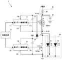
- FIG. 1 is a block diagram of a drive circuit according to an embodiment of the present invention.
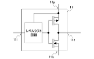
- FIG. 2 is an explanatory diagram of a configuration example of the first gate drive circuit.
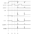
- FIG. 3 is a timing chart for explaining the operation of the drive circuit according to the embodiment.
- FIG. 4 is an explanatory diagram of a current path of the drive circuit according to the embodiment when FET # 2 is turned on.
- FIG. 5 is an explanatory diagram of a current path of the drive circuit according to the embodiment when FET # 1 is turned on.
- FIG. 1 is a diagram showing a configuration of an LD drive circuit 1 according to an embodiment of the present invention.
- the LD drive circuit 1 according to the present embodiment is a circuit developed on the assumption that it is provided for each laser diode 31 (hereinafter, also referred to as LD31) in the laser diode array 30.
- the drive circuits include a control circuit 10, a first gate drive circuit 11, a second gate drive circuit 12, FET # 1, FET # 2, a capacitor 13, a bypass capacitor 14, a diode 15, and a laser.
- a drive power source 25 is provided.
- the laser drive power source 25 is a power supply source for driving (light emitting) the LD 31.
- the laser drive power source 25 is composed of a resistor 26 and a capacitor 27 charged with a voltage of several tens to 100 V class from an LD power supply applied via the resistor 26.
- FET # 1 is a GaN-FET (Field Effect Transistor) for supplying the current (charge) from the capacitor 27 to the LD 31.
- the drain and gate of FET # 1 are connected to the output end of the laser drive power source 25 and the output port 11o of the first gate drive circuit 11, respectively. Further, the source of FET # 1 is connected to the anode of LD31, the negative voltage port 11n of the first gate drive circuit 11, and the like.
- the FET # 2 is for turning on / off the connection between the negative voltage port 11n of the first gate drive circuit 11 (and the anode of the LD31, the drain of the FET # 2 and the negative terminal of the capacitor 13) and the ground. It is a MOS (Metal Oxide Semiconductor) FET.
- the drain, gate, and source of FET # 2 are connected to the source of FET # 1 (and the negative voltage port 11n of the first gate drive circuit 11 and the like), the output port 12o of the second gate drive circuit 12, and the ground, respectively. ing.
- the device used as the FET # 2 does not have to be a MOSFET as long as it is a semiconductor switch capable of turning on / off the connection between the negative voltage port 11n and the ground, and a GaN-FET or the like may be used. You can also.
- the second gate drive circuit 12 has a positive voltage port 12p, a negative voltage port 12n, an input port 12i, and an output port 12o, and a signal of a predetermined level (high level in this embodiment) is input to the input port 12i. In this case, the circuit outputs the input voltage to the positive voltage port 12p from the output port 12o.
- the positive side voltage port 12p and the negative side voltage port 12n of the second gate drive circuit 12 are connected to the VDD power supply and the ground, respectively.
- the output voltage of the VDD power supply may be a voltage (for example, 5V) lower than the Vgs withstand voltage of FET # 1 (GaN-FET) in which the second gate drive circuit 12 or the like can operate. Just do it.
- the second gate drive circuit 12 a circuit similar to that of a general gate driver (for example, a push-pull circuit using two MOSFETs) can be used.
- a bypass capacitor 14 is arranged between the VDD power supply and the ground.
- the first gate drive circuit 11 has a positive voltage port 11p, a negative voltage port 11n, an input port 11i, and an output port 11o, and a signal of a predetermined level (high level in this embodiment) is input to the input port 11i. In this case, the circuit outputs the input voltage to the positive voltage port 11p from the output port 11o.
- FIG. 2 shows a configuration example of the first gate drive circuit 11.
- the first gate drive circuit 11 is a circuit in which both the potential of the positive voltage port 11p and the potential of the negative voltage port 11n change when FET # 1 is turned on. There is. Therefore, as the first gate drive circuit 11, for example, a circuit having a configuration as shown in FIG. 2, that is, a push-pull circuit using two MOSFETs and a gate of each MOSFET constituting the push-pull circuit. A circuit including a level shift circuit that changes the input voltage according to the potential of the positive voltage port 11p is used.
- the control circuit 10 sets the control signal level to the second gate drive circuit 12 to a high level during the first set time, waits for the elapse of the second set time, and then waits for the elapse of the second set time, and then the first gate during the third set time. It is a circuit configured to be able to execute laser drive processing in which the control signal level to the drive circuit 11 is set to a high level.
- the first to third set times are times set by the user.
- the first set time is determined in consideration of the time required for charging the capacitor 13, and the second set time is determined in consideration of the turn-off time of FET # 2.
- the third set time is set as a time equal to or longer than the pulse width of the laser (that is, the time when the charge charge of the capacitor 27 is completely discharged), and the timing of setting the high level determines the laser emission timing.
- the control circuit 10 has an operation mode in which the laser drive process is performed each time a predetermined instruction is input from the outside, and an operation mode in which the laser drive process is repeated at a set cycle.
- the drive circuit according to this embodiment has the configuration described above. Therefore, according to the drive circuit according to the present embodiment, the LD31 can be driven while suppressing the Vgs of FET # 1 (GaN-FET) to Vgs withstand voltage or less.
- FIG. 3 is a timing chart for explaining the operation of the drive circuit according to the present embodiment
- FIG. 4 is an explanatory diagram of a current path when FET # 2 of the drive circuit according to the present embodiment is turned on
- FIG. 5 is the present embodiment. It is explanatory drawing of the current path at the time of FET # 1 of the drive circuit which concerns on.
- the supply of VDD power is already started
- the supply of LD power is started at time T1 with the FETs # 1 and # 2 off and the capacitor 27 not charged. ..
- the potential of the node N101 is not the ground potential.
- FET # 2 is turned off at time T3 after the charging of the capacitor 13 is completed. Then, when FET # 1 is turned on at time T4, a current flows in the path shown in FIG. 5 and pulsed light is emitted from the LD 31, but the first gate drive circuit 11 has a negative voltage.
- the capacitor 13 operates as a power source while the port 11n is connected to the node N101. Therefore, as shown in FIG. 3, the Vgs of the FET # 1 is always suppressed to the Vgs withstand voltage or less (while the FET # 1 is on or off).
- an LD having a cathode connected to the ground (LD31 or the like in the cathode common type LD array 30) can be satisfactorily driven by a GaN-FET. .. Therefore, by using the LD drive circuit 1 according to the present embodiment, it is possible to realize a high-performance device (for example, a distance measuring device such as LiDAR or a processing device) that uses a pulsed laser beam.
- a high-performance device for example, a distance measuring device such as LiDAR or a processing device
- the drive circuit of the above-described embodiment can be modified in various ways.
- the drive circuit may be transformed into a circuit that does not include the control circuit 10 (that is, a circuit in which control signals are input to the first gate drive circuit 11 and the second gate drive circuit 12 from the outside).
- the drive circuit is transformed into a circuit that does not include the control circuit 10 and the second gate drive circuit 12 (that is, a circuit in which a control signal is input to the first gate drive circuit 11 and FET # 2 from the outside). good.
- the configuration may not include the bypass capacitor 14.
- a resistor may be inserted between the diode 15 and the positive voltage port 11p, and the circuit configuration of the first gate drive circuit 11 does not have to be the one described above. is there.
- a GaN-FET (FET # 1) having a source connected to the anode of the laser diode (31) and a drain connected to the power source (25) of the laser diode (31). When it has a positive voltage port (11p), a negative voltage port (11n), an input port (11i), and an output port (11o), and a predetermined level signal is input to the input port (11i),
- a gate drive circuit (11) that outputs an input voltage to the positive voltage port (11p) from the output port (11o), and the output port (11o) and the negative voltage port are the GaN, respectively.
Landscapes
- Physics & Mathematics (AREA)
- Condensed Matter Physics & Semiconductors (AREA)
- General Physics & Mathematics (AREA)
- Electromagnetism (AREA)
- Optics & Photonics (AREA)
- Semiconductor Lasers (AREA)
Abstract
駆動回路(1)は、LD(31)のアノードにソース(S)が接続され、LD(31)の電力源(25)にドレイン(D)が接続されたGaN-FET(FET#1)と、所定レベルの信号の入力時に、正側電圧ポート(11p)への入力電圧を出力ポート(11o)から出力する、出力ポート(11o)、負側電圧ポート(11n)が、それぞれ、GaN-FET(FET#1)のゲート(G)、ソース(S)と接続されたゲート駆動回路(11)と、ゲート駆動回路(11)の正側電圧ポート(11p)と負側電圧ポート(11n)との間に配置されたコンデンサ(13)と、ゲート駆動回路(11)の正側電圧ポート(11p)と、GaN-FET(FET#1)のVgs耐圧未満の電圧を出力するVDD電源とを接続する電源ラインに、正側電圧ポート(11p)からVDD電源に向けて流れる電流を遮断する向きで挿入されたダイオード(15)と、GaN-FET(FET#1)のソース(S)とグラウンドとの間に配置された半導体スイッチ(FET#2)と、を備える。
Description
本発明は、レーザーダイオードを駆動するための駆動回路に関する。
コンデンサに充電した電荷を半導体スイッチを介して供給することでレーザーダイオード(以下、LDとも表記する)をパルス駆動する場合(特許文献1、2参照)、半導体スイッチのスイッチング速度が速い方がパルス形状を良好なものとすることができる。従って、LDのパルス駆動時には半導体スイッチとして、GaN-FET(Field Effect Transistor)を使用するニーズが存在する。
ただし、一般的なLDアレイは、カソードコモン型のものであるため、一般的なLDアレイの各LDをそれぞれ独立で高速にパルス駆動させたい場合にGaN-FETを使用する際には、各LDのアノードにGaN-FETのソースが接続されることが望ましい。
LDのアノードにGaN-FETのソースが接続されている場合には、GaN-FETのオンによりLDに電流が流れると、LDのアノード電位(即ち、GaN-FETのソース電位)が大きく変化する。そして、GaN-FETのVgs耐圧は、低い(6V程度)ため、Vgsをこの電圧以下に抑えながら、LDのアノード側に接続されているGaN-FETをON/OFF制御することは困難であった。
本発明は、上記問題に鑑みなされたものであり、カソードがグラウンドに接続されたLD(例えば、カソードコモン型のLDアレイ中のLD等)をGaN-FETにより良好に駆動できる駆動回路を提供することを目的とする。
本発明の一観点に係る駆動回路は、レーザーダイオードを駆動するための駆動回路であって、
前記レーザーダイオードのアノードにソースが接続され、前記レーザーダイオードの電力源にドレインが接続されたGaN-FETと、
正側電圧ポート、負側電圧ポート、入力ポート、出力ポートを有し、所定レベルの信号が前記入力ポートに入力されている場合に、前記正側電圧ポートへの入力電圧を前記出力ポートから出力するゲート駆動回路であって、前記出力ポート、前記負側電圧ポートが、それぞれ、前記GaN-FETのゲート、ソースと接続されたゲート駆動回路と、
前記ゲート駆動回路の前記正側電圧ポートと前記負側電圧ポートとの間に配置されたコンデンサと、
前記ゲート駆動回路の前記正側電圧ポートと、前記GaN-FETのVgs耐圧未満の電圧を出力するVDD電源とを接続する電源ラインに、前記正側電圧ポートから前記VDD電源に向けて流れる電流を遮断する向きで挿入されたダイオードと
前記GaN-FETのソースとグラウンドとの間の接続をON/OFFするための半導体スイッチと、
を備える。
前記レーザーダイオードのアノードにソースが接続され、前記レーザーダイオードの電力源にドレインが接続されたGaN-FETと、
正側電圧ポート、負側電圧ポート、入力ポート、出力ポートを有し、所定レベルの信号が前記入力ポートに入力されている場合に、前記正側電圧ポートへの入力電圧を前記出力ポートから出力するゲート駆動回路であって、前記出力ポート、前記負側電圧ポートが、それぞれ、前記GaN-FETのゲート、ソースと接続されたゲート駆動回路と、
前記ゲート駆動回路の前記正側電圧ポートと前記負側電圧ポートとの間に配置されたコンデンサと、
前記ゲート駆動回路の前記正側電圧ポートと、前記GaN-FETのVgs耐圧未満の電圧を出力するVDD電源とを接続する電源ラインに、前記正側電圧ポートから前記VDD電源に向けて流れる電流を遮断する向きで挿入されたダイオードと
前記GaN-FETのソースとグラウンドとの間の接続をON/OFFするための半導体スイッチと、
を備える。
すなわち、この駆動回路は、半導体スイッチをオンすれば、ゲート駆動回路のフローティング電源として機能するコンデンサが、GaN-FETのVgs耐圧未満の電圧に設定されたVDD電源の出力電圧で充電される構成を有する。しかも、駆動回路のコンデンサの低電位側端子(即ち、ゲート駆動回路の負側電圧ポートと接続されている端子)は、GaN-FETのソース(及びレーザーダイオードのアノード)と接続されている。従って、本駆動回路によって、カソードコモン型のLDアレイ中のLD等を駆動すれば、常に(即ち、GaN-FETがONであってもOFFであっても)、GaN-FETのVgsがVgs耐圧未満に制御されることになる。
また、前記半導体スイッチが、前記GaN-FETのソース(即ち、前記コンデンサの低電位側端子と接続されている端子)とグラウンドとの間の接続をON/OFFすることにより、フローティング電源として機能するコンデンサを動作毎に安定して充電させることができる。
駆動回路は、半導体スイッチのON/OFF制御、及び、GaN-FETのON/OFF制御(即ち、ゲート駆動回路への制御信号のレベル制御)が、駆動回路外の装置/回路によって行われる回路であっても良い。また、駆動回路に、前記半導体スイッチを第1所定時間の間だけオンさせるための制御をおこなった後に、前記ゲート駆動回路の前記入力ポートに前記所定レベルの信号を第2所定時間の間だけ供給する制御回路を、設けておいても良い。
本発明によれば、カソードコモン型のLDアレイ中のLD等をGaN-FETにより良好に駆動できる駆動回路を提供することができる。
以下、本発明の実施の形態を、図面を参照して説明する。
図1は、本発明の一実施形態に係るLD駆動回路1の構成を示す図である。本実施形態に係るLD駆動回路1は、レーザーダイオードアレイ30内のレーザーダイオード31(以下、LD31とも表記する)毎に設けられることを想定して開発した回路である。図示してあるように、駆動回路は、制御回路10、第1ゲート駆動回路11、第2ゲート駆動回路12、FET#1、FET#2、コンデンサ13、バイパスコンデンサ14、ダイオード15、及び、レーザ駆動電力源25を備える。
レーザ駆動電力源25は、LD31を駆動(発光)させるための電力の供給源である。レーザ駆動電力源25は、抵抗26と、抵抗26を介して印加されるLD電源からの、数10~100V級の電圧で充電されるコンデンサ27とにより構成されている。
FET#1は、コンデンサ27からの電流(電荷)をLD31に供給するためのGaN-FET(Field Effect Transistor)である。FET#1のドレイン、ゲートは、それぞれ、レーザ駆動電力源25の出力端、第1ゲート駆動回路11の出力ポート11oに接続されている。また、FET#1のソースは、LD31のアノード、第1ゲート駆動回路11の負側電圧ポート11n等に接続されている。以下、レーザ駆動電力源25の出力端(レーザ駆動電力源25とFET#1のドレインとの接続箇所)のことを、ノードN102と表記し、FET#1のソースと第1ゲート駆動回路11の負側電圧ポート11nとの接続箇所のことを、ノードN101と表記する。
FET#2は、第1ゲート駆動回路11の負側電圧ポート11n(及びLD31のアノード、FET#2のドレイン及びコンデンサ13の負側端子)とグラウンドとの間の接続をON/OFFするためのMOS(Metal Oxide Semiconductor )FETである。FET#2のドレイン、ゲート、ソースは、それぞれ、FET#1のソース(及び第1ゲート駆動回路11の負側電圧ポート11n等)、第2ゲート駆動回路12の出力ポート12o、グラウンドに接続されている。このFET#2として使用するデバイスは、負側電圧ポート11nとグラウンドとの間の接続をON/OFF可能な半導体スイッチでありさえすれば、MOSFETでなくても良く、GaN-FET等を用いることもできる。
第2ゲート駆動回路12は、正側電圧ポート12p、負側電圧ポート12n、入力ポート12i、出力ポート12oを有し、所定レベル(本実施形態では、ハイレベル)の信号が入力ポート12iに入力されている場合に、正側電圧ポート12pへの入力電圧を出力ポート12oから出力する回路である。この第2ゲート駆動回路12の正側電圧ポート12p、負側電圧ポート12nは、それぞれ、VDD電源、グラウンドに接続されている。なお、VDD電源の出力電圧(以下、単にVDDともいう)は、第2ゲート駆動回路12等が動作可能な、FET#1(GaN-FET)のVgs耐圧未満の電圧(例えば、5V)であればよい。また、第2ゲート駆動回路12としては、一般的なゲートドライバと同様の回路(例えば、2つのMOSFETによるプッシュプル回路)を使用することができる。また、図1に示すように、VDD電源とグラウンドとの間にはバイパスコンデンサ14が配置されている。
第1ゲート駆動回路11は、正側電圧ポート11p、負側電圧ポート11n、入力ポート11i、出力ポート11oを有し、所定レベル(本実施形態では、ハイレベル)の信号が入力ポート11iに入力されている場合に、正側電圧ポート11pへの入力電圧を出力ポート11oから出力する回路である。図2に、第1ゲート駆動回路11の構成例を示す。
図1に示すように、第1ゲート駆動回路11の正側電圧ポート11pと負側電圧ポート11nとの間には、コンデンサ13が配置されている。さらに、第1ゲート駆動回路11の正側電圧ポート11pと、VDD電源とは、正側電圧ポート11pからVDD電源に向けて流れる電流を遮断するためのダイオード15が挿入された電源ラインにて接続されている。また、既に説明したように、第1ゲート駆動回路11の負側電圧ポート11nは、FET#1のソース、FET#2のドレイン及びLD31のアノードと接続されている。
ここまでの説明から明らかなように、第1ゲート駆動回路11は、FET#1がONされると、正側電圧ポート11pの電位と負側電圧ポート11nの電位が共に変化する回路となっている。そのため、第1ゲート駆動回路11としては、例えば、図2に示したような構成の回路、すなわち、2つのMOSFETによるプッシュプル回路と、当該プッシュプル回路を構成している各MOSFETのゲートへの入力電圧を、正側電圧ポート11pの電位に応じて変更するレベルシフト回路とを備えた回路が使用される。
制御回路10は、第1設定時間の間、第2ゲート駆動回路12への制御信号レベルをハイレベルとし、第2設定時間の経過を待機してから、第3設定時間の間、第1ゲート駆動回路11への制御信号レベルをハイレベルとするレーザ駆動処理を実行可能に構成された回路である。なお、第1~第3設定時間とは、ユーザにより設定される時間のことである。第1設定時間は、コンデンサ13の充電に要する時間を考慮して定められ、第2設定時間は、FET#2のターンオフ時間を考慮して定められる。また、第3設定時間は、レーザのパルス幅(即ち、コンデンサ27の充電電荷が放電しきる時間)以上の時間として定められ、ハイレベルとするタイミングがレーザ発光タイミングを決定する。
制御回路10は、外部から所定の指示が入力される度にレーザ駆動処理を行う動作モードと、設定された周期でレーザ駆動処理を繰り返す動作モードとを有している。
本実施形態に係る駆動回路は、以上説明した構成を有している。従って、本実施形態に係る駆動回路によれば、FET#1(GaN-FET)のVgsを、Vgs耐圧以下に抑えながら、LD31を駆動することができる。
以下、図3から図5に基づいて本実施形態に係る駆動回路の動作例を説明する。図3は、本実施形態に係る駆動回路の動作を説明するためのタイミングチャート、図4は本実施形態に係る駆動回路のFET#2オン時の電流経路の説明図、図5は本実施形態に係る駆動回路のFET#1オン時の電流経路の説明図である。以下の説明では、VDD電源の供給はすでに開始されており、FET#1、#2がオフ、コンデンサ27が未充電の状態で、時刻T1にLD電源の供給が開始された場合を前提とする。なお、ノードN101の電位は、グラウンド電位ではないとする。
図3に示すように、時刻T1にLD電源の供給が開始されると、コンデンサ27の充電が開始されるため、ノードN102の電位V_N102が上昇して、所定時間後に、V_N102がLD電源の電位となる。
そして、制御回路10の制御により時刻T2にFET#2がオンされると、ノードN101の電位V_N101がグラウンド電位となる。また、図4に示した経路で電流が流れることになるため、コンデンサ13が充電されてコンデンサ13の両端間の電圧がほぼVDD(即ち、Vgs耐圧以下の電圧)となる。
コンデンサ13の充電完了後の時刻T3にFET#2がオフされる。そして、時刻T4にFET#1がオンされると、図5に示した経路で電流が流れて、LD31からパルス光が射出されることになるが、第1ゲート駆動回路11は、負側電圧ポート11nがノードN101と接続された状態でコンデンサ13を電源として動作している。従って、図3に示してあるように、常に(FET#1のオン時やオフしている間)、FET#1のVgsが、Vgs耐圧以下に抑えられることになる。
以上、説明したように、本実施形態に係るLD駆動回路1によれば、カソードがグラウンドに接続されたLD(カソードコモン型のLDアレイ30中のLD31等)をGaN-FETにより良好に駆動できる。従って、本実施形態に係るLD駆動回路1を用いることで、パルスレーザ光を用いる、高性能な装置(例えば、LiDAR等の測距装置や加工装置)を実現できる。
《変形形態》
上記した実施形態の駆動回路は、各種の変形が可能なものである。例えば、駆動回路を、制御回路10を備えない回路(即ち、外部から、第1ゲート駆動回路11、第2ゲート駆動回路12への制御信号が入力される回路)に変形しても良い。また、駆動回路を、制御回路10及び第2ゲート駆動回路12を備えない回路(即ち、外部から第1ゲート駆動回路11、FET#2への制御信号が入力される回路)に変形しても良い。また、バイパスコンデンサ14を備えない構成であっても良い。また、ダイオード15と正側電圧ポート11pとの間に抵抗を挿入しても良いことや、第1ゲート駆動回路11の回路構成が上記したものでなくても良いことなどは、当然のことである。
上記した実施形態の駆動回路は、各種の変形が可能なものである。例えば、駆動回路を、制御回路10を備えない回路(即ち、外部から、第1ゲート駆動回路11、第2ゲート駆動回路12への制御信号が入力される回路)に変形しても良い。また、駆動回路を、制御回路10及び第2ゲート駆動回路12を備えない回路(即ち、外部から第1ゲート駆動回路11、FET#2への制御信号が入力される回路)に変形しても良い。また、バイパスコンデンサ14を備えない構成であっても良い。また、ダイオード15と正側電圧ポート11pとの間に抵抗を挿入しても良いことや、第1ゲート駆動回路11の回路構成が上記したものでなくても良いことなどは、当然のことである。
《付記》
レーザーダイオード(31)を駆動するための駆動回路(1)であって、
前記レーザーダイオード(31)のアノードにソースが接続され、前記レーザーダイオード(31)の電力源(25)にドレインが接続されたGaN-FET(FET#1)と、
正側電圧ポート(11p)、負側電圧ポート(11n)、入力ポート(11i)、出力ポート(11o)を有し、所定レベルの信号が前記入力ポート(11i)に入力されている場合に、前記正側電圧ポート(11p)への入力電圧を前記出力ポート(11o)から出力するゲート駆動回路(11)であって、前記出力ポート(11o)、前記負側電圧ポートが、それぞれ、前記GaN-FET(FET#1)のゲート、ソースと接続されたゲート駆動回路(11)と、
前記ゲート駆動回路(11)の前記正側電圧ポート(11p)と前記負側電圧ポート(11n)との間に配置されたコンデンサ(13)と、
前記ゲート駆動回路(11)の前記正側電圧ポート(11p)と、前記GaN-FET(FET#1)のVgs耐圧未満の電圧を出力するVDD電源とを接続する電源ラインに、前記正側電圧ポート(11p)から前記VDD電源に向けて流れる電流を遮断する向きで挿入されたダイオード(15)と
前記GaN-FET(FET#1)のソースとグラウンドとの間の接続をON/OFFするための半導体スイッチ(FET#2)と、
を備えることを特徴とする駆動回路(1)。
レーザーダイオード(31)を駆動するための駆動回路(1)であって、
前記レーザーダイオード(31)のアノードにソースが接続され、前記レーザーダイオード(31)の電力源(25)にドレインが接続されたGaN-FET(FET#1)と、
正側電圧ポート(11p)、負側電圧ポート(11n)、入力ポート(11i)、出力ポート(11o)を有し、所定レベルの信号が前記入力ポート(11i)に入力されている場合に、前記正側電圧ポート(11p)への入力電圧を前記出力ポート(11o)から出力するゲート駆動回路(11)であって、前記出力ポート(11o)、前記負側電圧ポートが、それぞれ、前記GaN-FET(FET#1)のゲート、ソースと接続されたゲート駆動回路(11)と、
前記ゲート駆動回路(11)の前記正側電圧ポート(11p)と前記負側電圧ポート(11n)との間に配置されたコンデンサ(13)と、
前記ゲート駆動回路(11)の前記正側電圧ポート(11p)と、前記GaN-FET(FET#1)のVgs耐圧未満の電圧を出力するVDD電源とを接続する電源ラインに、前記正側電圧ポート(11p)から前記VDD電源に向けて流れる電流を遮断する向きで挿入されたダイオード(15)と
前記GaN-FET(FET#1)のソースとグラウンドとの間の接続をON/OFFするための半導体スイッチ(FET#2)と、
を備えることを特徴とする駆動回路(1)。
1・・・LD駆動回路
10・・・制御回路
11p,12p・・・正側電圧ポート
11o,12o・・・出力ポート
11i,12i・・・入力ポート
11n,12n・・・負側電圧ポート
11・・・第1ゲート駆動回路
12・・・第2ゲート駆動回路
13,27・・・コンデンサ
14・・・バイパスコンデンサ
15・・・ダイオード
25・・・レーザ駆動電力源
26・・・抵抗
30・・・レーザーダイオードアレイ
31・・・レーザーダイオード
10・・・制御回路
11p,12p・・・正側電圧ポート
11o,12o・・・出力ポート
11i,12i・・・入力ポート
11n,12n・・・負側電圧ポート
11・・・第1ゲート駆動回路
12・・・第2ゲート駆動回路
13,27・・・コンデンサ
14・・・バイパスコンデンサ
15・・・ダイオード
25・・・レーザ駆動電力源
26・・・抵抗
30・・・レーザーダイオードアレイ
31・・・レーザーダイオード
Claims (2)
- レーザーダイオードを駆動するための駆動回路であって、
前記レーザーダイオードのアノードにソースが接続され、前記レーザーダイオードの電力源にドレインが接続されたGaN-FETと、
正側電圧ポート、負側電圧ポート、入力ポート、出力ポートを有し、所定レベルの信号が前記入力ポートに入力されている場合に、前記正側電圧ポートへの入力電圧を前記出力ポートから出力するゲート駆動回路であって、前記出力ポート、前記負側電圧ポートが、それぞれ、前記GaN-FETのゲート、ソースと接続されたゲート駆動回路と、
前記ゲート駆動回路の前記正側電圧ポートと前記負側電圧ポートとの間に配置されたコンデンサと、
前記ゲート駆動回路の前記正側電圧ポートと、前記GaN-FETのVgs耐圧未満の電圧を出力するVDD電源とを接続する電源ラインに、前記正側電圧ポートから前記VDD電源に向けて流れる電流を遮断する向きで挿入されたダイオードと
前記GaN-FETのソースとグラウンドとの間の接続をON/OFFするための半導体スイッチと、
を備えることを特徴とする駆動回路。 - 前記半導体スイッチを第1所定時間の間だけオンさせるための制御をおこなった後に、前記ゲート駆動回路の前記入力ポートに前記所定レベルの信号を第2所定時間の間だけ供給する制御回路を、さらに備える、
ことを特徴とする請求項1に記載の駆動回路。
Priority Applications (3)
| Application Number | Priority Date | Filing Date | Title |
|---|---|---|---|
| EP20853407.3A EP3993185B1 (en) | 2019-08-09 | 2020-07-28 | Drive circuit |
| CN202080055230.1A CN114207968B (zh) | 2019-08-09 | 2020-07-28 | 驱动电路 |
| US17/630,190 US12155174B2 (en) | 2019-08-09 | 2020-07-28 | Drive circuit |
Applications Claiming Priority (2)
| Application Number | Priority Date | Filing Date | Title |
|---|---|---|---|
| JP2019-147172 | 2019-08-09 | ||
| JP2019147172A JP7275984B2 (ja) | 2019-08-09 | 2019-08-09 | 駆動回路 |
Publications (1)
| Publication Number | Publication Date |
|---|---|
| WO2021029218A1 true WO2021029218A1 (ja) | 2021-02-18 |
Family
ID=74571063
Family Applications (1)
| Application Number | Title | Priority Date | Filing Date |
|---|---|---|---|
| PCT/JP2020/028853 Ceased WO2021029218A1 (ja) | 2019-08-09 | 2020-07-28 | 駆動回路 |
Country Status (5)
| Country | Link |
|---|---|
| US (1) | US12155174B2 (ja) |
| EP (1) | EP3993185B1 (ja) |
| JP (1) | JP7275984B2 (ja) |
| CN (1) | CN114207968B (ja) |
| WO (1) | WO2021029218A1 (ja) |
Families Citing this family (3)
| Publication number | Priority date | Publication date | Assignee | Title |
|---|---|---|---|---|
| WO2023028526A1 (en) * | 2021-08-25 | 2023-03-02 | The Regents Of The University Of California | Bi-directional synchronous bootstrapping |
| WO2023238786A1 (ja) | 2022-06-08 | 2023-12-14 | 株式会社小糸製作所 | 発光装置 |
| CN118712875B (zh) * | 2024-06-14 | 2025-01-28 | 天津大学 | 一种带负电压过流保护的恒温恒流半导体激光器驱动电路 |
Citations (7)
| Publication number | Priority date | Publication date | Assignee | Title |
|---|---|---|---|---|
| JPS559537B2 (ja) | 1976-10-01 | 1980-03-11 | ||
| JPH0896394A (ja) * | 1994-07-25 | 1996-04-12 | Olympus Optical Co Ltd | 光ディスク用レーザ駆動装置 |
| JP2006310684A (ja) * | 2005-05-02 | 2006-11-09 | Sony Corp | 駆動回路 |
| JP2011023474A (ja) * | 2009-07-14 | 2011-02-03 | Sumitomo Electric Ind Ltd | 半導体レーザ駆動回路 |
| JP2011238821A (ja) * | 2010-05-12 | 2011-11-24 | Canon Inc | 半導体レーザ素子駆動装置 |
| JP2017216812A (ja) * | 2016-05-31 | 2017-12-07 | 浜松ホトニクス株式会社 | 昇圧回路 |
| US20180278017A1 (en) * | 2017-03-23 | 2018-09-27 | Infineon Technologies Ag | Circuit and method for driving a laser diode |
Family Cites Families (17)
| Publication number | Priority date | Publication date | Assignee | Title |
|---|---|---|---|---|
| JPS622580A (ja) * | 1985-06-27 | 1987-01-08 | Fujitsu Ltd | レ−ザダイオ−ド駆動回路 |
| JP2713342B2 (ja) * | 1988-03-31 | 1998-02-16 | 富士通株式会社 | 光半導体素子駆動回路 |
| JP2007042731A (ja) * | 2005-08-01 | 2007-02-15 | Olympus Corp | パルス電源装置 |
| EP1882899A1 (de) | 2006-07-17 | 2008-01-30 | Leica Geosystems AG | Elektrooptischer Entfernungsmesser |
| JP5509537B2 (ja) | 2008-04-16 | 2014-06-04 | セイコーエプソン株式会社 | プロジェクタおよびその駆動方法 |
| JP2012009651A (ja) * | 2010-06-25 | 2012-01-12 | Panasonic Corp | 電流駆動装置 |
| CN101895058B (zh) * | 2010-07-07 | 2011-11-16 | 中国科学院上海光学精密机械研究所 | 用于半导体激光器的高速窄脉冲调制驱动电源 |
| US8593211B2 (en) * | 2012-03-16 | 2013-11-26 | Texas Instruments Incorporated | System and apparatus for driver circuit for protection of gates of GaN FETs |
| US9461642B1 (en) * | 2015-08-26 | 2016-10-04 | Southwest Research Institute | Radiation-tolerant high-speed high-voltage pulser |
| US10158211B2 (en) * | 2015-09-22 | 2018-12-18 | Analog Devices, Inc. | Pulsed laser diode driver |
| US9966837B1 (en) * | 2016-07-08 | 2018-05-08 | Vpt, Inc. | Power converter with circuits for providing gate driving |
| JP6683825B2 (ja) * | 2016-10-20 | 2020-04-22 | 日本電信電話株式会社 | 直接変調レーザ駆動回路 |
| TWI732280B (zh) * | 2018-08-28 | 2021-07-01 | 美商高效電源轉換公司 | 串級自舉式GaN功率開關及驅動器 |
| TWI715167B (zh) * | 2018-08-28 | 2021-01-01 | 美商高效電源轉換公司 | 基於GaN的高電流驅動器之故障安全停機技術 |
| TWI716980B (zh) * | 2018-08-28 | 2021-01-21 | 美商高效電源轉換公司 | 使用具回授之主動前置驅動器的GaN驅動器 |
| US11687110B2 (en) * | 2018-09-26 | 2023-06-27 | Efficient Power Conversion Corporation | Multi-channel pulse current generator with charging |
| KR102797771B1 (ko) * | 2019-04-29 | 2025-04-22 | 이피션트 파워 컨버젼 코퍼레이션 | 게이트 전류 재사용을 이용한 GaN 레이저 다이오드 구동 FET |
-
2019
- 2019-08-09 JP JP2019147172A patent/JP7275984B2/ja active Active
-
2020
- 2020-07-28 EP EP20853407.3A patent/EP3993185B1/en active Active
- 2020-07-28 CN CN202080055230.1A patent/CN114207968B/zh active Active
- 2020-07-28 WO PCT/JP2020/028853 patent/WO2021029218A1/ja not_active Ceased
- 2020-07-28 US US17/630,190 patent/US12155174B2/en active Active
Patent Citations (7)
| Publication number | Priority date | Publication date | Assignee | Title |
|---|---|---|---|---|
| JPS559537B2 (ja) | 1976-10-01 | 1980-03-11 | ||
| JPH0896394A (ja) * | 1994-07-25 | 1996-04-12 | Olympus Optical Co Ltd | 光ディスク用レーザ駆動装置 |
| JP2006310684A (ja) * | 2005-05-02 | 2006-11-09 | Sony Corp | 駆動回路 |
| JP2011023474A (ja) * | 2009-07-14 | 2011-02-03 | Sumitomo Electric Ind Ltd | 半導体レーザ駆動回路 |
| JP2011238821A (ja) * | 2010-05-12 | 2011-11-24 | Canon Inc | 半導体レーザ素子駆動装置 |
| JP2017216812A (ja) * | 2016-05-31 | 2017-12-07 | 浜松ホトニクス株式会社 | 昇圧回路 |
| US20180278017A1 (en) * | 2017-03-23 | 2018-09-27 | Infineon Technologies Ag | Circuit and method for driving a laser diode |
Non-Patent Citations (1)
| Title |
|---|
| See also references of EP3993185A4 |
Also Published As
| Publication number | Publication date |
|---|---|
| CN114207968B (zh) | 2024-08-20 |
| JP7275984B2 (ja) | 2023-05-18 |
| CN114207968A (zh) | 2022-03-18 |
| EP3993185B1 (en) | 2025-10-29 |
| EP3993185A1 (en) | 2022-05-04 |
| US20220294183A1 (en) | 2022-09-15 |
| US12155174B2 (en) | 2024-11-26 |
| JP2021028924A (ja) | 2021-02-25 |
| EP3993185A4 (en) | 2023-08-23 |
Similar Documents
| Publication | Publication Date | Title |
|---|---|---|
| US10756722B2 (en) | Hybrid switch control | |
| US10535977B1 (en) | GaNFET as energy store for fast laser pulser | |
| US9973188B2 (en) | Switch driving device and switch driving method | |
| US10211826B2 (en) | Electronic switch, and corresponding device and method | |
| US10177758B2 (en) | Driver for a P-channel MOSFET | |
| TWI439022B (zh) | 具電壓箝位功能的閘極驅動電路 | |
| TWI743752B (zh) | 具閘極電流再利用功能之氮化鎵雷射二極體驅動場效電晶體 | |
| CN110071715B (zh) | 使用低压器件的高量程正电压电平移位器 | |
| JP7275984B2 (ja) | 駆動回路 | |
| US20110050316A1 (en) | Power transistor with turn off control and method for operating | |
| JP2021535702A5 (ja) | ||
| WO2016177197A1 (zh) | 一种单电源电路和电源系统 | |
| CN106462176A (zh) | 用于感测和控制电流的方法和电路 | |
| JP2013042612A (ja) | ゲート駆動回路 | |
| CN101399512A (zh) | 风扇驱动系统 | |
| CN102577124A (zh) | 高压开关配置 | |
| CA3040184A1 (en) | Ganfet as energy store for fast laser pulser | |
| CN111884637A (zh) | 自举电路和功率芯片 | |
| JP2025176930A (ja) | 出力回路 | |
| TW202612237A (zh) | 驅動單元 | |
| CN115622017A (zh) | 一种反向保护电路及负载开关 | |
| JP2005287258A (ja) | ゲート駆動回路 | |
| KR20020043975A (ko) | 전동차량의 병렬 구동 fet의 구동 전류 증폭 회로 및방법 |
Legal Events
| Date | Code | Title | Description |
|---|---|---|---|
| 121 | Ep: the epo has been informed by wipo that ep was designated in this application |
Ref document number: 20853407 Country of ref document: EP Kind code of ref document: A1 |
|
| NENP | Non-entry into the national phase |
Ref country code: DE |
|
| ENP | Entry into the national phase |
Ref document number: 2020853407 Country of ref document: EP Effective date: 20220131 |
|
| WWG | Wipo information: grant in national office |
Ref document number: 2020853407 Country of ref document: EP |