WO2021029254A1 - コネクタ用端子材 - Google Patents
コネクタ用端子材 Download PDFInfo
- Publication number
- WO2021029254A1 WO2021029254A1 PCT/JP2020/029688 JP2020029688W WO2021029254A1 WO 2021029254 A1 WO2021029254 A1 WO 2021029254A1 JP 2020029688 W JP2020029688 W JP 2020029688W WO 2021029254 A1 WO2021029254 A1 WO 2021029254A1
- Authority
- WO
- WIPO (PCT)
- Prior art keywords
- silver
- plating layer
- nickel
- nickel alloy
- less
- Prior art date
- Legal status (The legal status is an assumption and is not a legal conclusion. Google has not performed a legal analysis and makes no representation as to the accuracy of the status listed.)
- Ceased
Links
Images


Classifications
-
- C—CHEMISTRY; METALLURGY
- C22—METALLURGY; FERROUS OR NON-FERROUS ALLOYS; TREATMENT OF ALLOYS OR NON-FERROUS METALS
- C22C—ALLOYS
- C22C5/00—Alloys based on noble metals
- C22C5/06—Alloys based on silver
-
- C—CHEMISTRY; METALLURGY
- C25—ELECTROLYTIC OR ELECTROPHORETIC PROCESSES; APPARATUS THEREFOR
- C25D—PROCESSES FOR THE ELECTROLYTIC OR ELECTROPHORETIC PRODUCTION OF COATINGS; ELECTROFORMING; APPARATUS THEREFOR
- C25D5/00—Electroplating characterised by the process; Pretreatment or after-treatment of workpieces
- C25D5/10—Electroplating with more than one layer of the same or of different metals
- C25D5/12—Electroplating with more than one layer of the same or of different metals at least one layer being of nickel or chromium
- C25D5/14—Electroplating with more than one layer of the same or of different metals at least one layer being of nickel or chromium two or more layers being of nickel or chromium, e.g. duplex or triplex layers
-
- H—ELECTRICITY
- H01—ELECTRIC ELEMENTS
- H01R—ELECTRICALLY-CONDUCTIVE CONNECTIONS; STRUCTURAL ASSOCIATIONS OF A PLURALITY OF MUTUALLY-INSULATED ELECTRICAL CONNECTING ELEMENTS; COUPLING DEVICES; CURRENT COLLECTORS
- H01R13/00—Details of coupling devices of the kinds covered by groups H01R12/70 or H01R24/00 - H01R33/00
- H01R13/02—Contact members
- H01R13/03—Contact members characterised by the material, e.g. plating, or coating materials
Definitions
- the present invention relates to a terminal material for a connector provided with a useful film used for connecting electrical wiring of automobiles, consumer devices, etc. to which a high current and a high voltage are applied.
- This application claims priority based on Japanese Patent Application No. 2019-146951 filed in Japan on August 9, 2019 and Japanese Patent Application No. 2020-078202 filed in Japan on April 27, 2020. The contents are used here.
- in-vehicle connectors used for connecting electrical wiring of automobiles and the like are known.
- the in-vehicle connector (in-vehicle terminal) is designed so that the contact piece provided in the female terminal and the male terminal inserted in the female terminal come into contact with each other at a predetermined contact pressure to be electrically connected. It has a pair of terminals.
- a tin-plated terminal that is generally tin-plated on a copper or copper alloy plate and reflowed is often used.
- the applications of precious metal-plated terminals having excellent heat resistance and wear resistance, which allow a larger current to flow, are increasing.
- the silver-plated terminal for a connector described in Patent Document 1 As an in-vehicle terminal that is required to have such heat resistance and wear resistance, for example, the silver-plated terminal for a connector described in Patent Document 1 is known.
- the silver-plated terminal for a connector described in Patent Document 1 the surface of a base material made of copper or a copper alloy is coated with a silver-plated layer.
- This silver plating layer has a first silver plating layer located on the lower layer side (base material side) and a second silver plating layer located on the upper layer side of the first silver plating layer, and has a first silver.
- the crystal grain size of the plating layer is formed to be larger than the crystal grain size of the second silver plating layer. That is, in the configuration of Patent Document 1, the crystal grain size of the first silver plating layer is formed to be larger than the crystal grain size of the second silver plating layer, so that the copper from the base material is formed into the second silver plating layer. It suppresses the spread to.
- Patent Document 2 a silver or silver alloy layer having an antimony concentration of 0.1% by mass or less is formed on at least a part of the surface of a copper or copper alloy member as a base material, and is formed on the silver or silver alloy layer.
- a copper or copper alloy member having a silver alloy layer having a Vickers hardness of HV140 or more having an antimony concentration of 0.5% by mass or more as the outermost layer is disclosed. That is, in the configuration of Patent Document 2, antimony is added to the silver or silver alloy layer to increase the hardness and improve the wear resistance of the copper or copper alloy member.
- the hardness of the silver-plated layer covering the surface of the base material decreases as the crystal grain size of silver increases (coarseness) due to aging and use in a high temperature environment. Reduced wear resistance over time and in high temperature environments. In order to compensate for this decrease in wear resistance, it is conceivable to increase the film thickness of the silver plating layer, but there is a problem in terms of cost.
- the present invention has been made in view of such circumstances, and an object of the present invention is to provide a terminal material for a connector capable of improving wear resistance and heat resistance.
- the terminal material for a connector of the present invention has at least a base material whose surface layer is made of copper or a copper alloy, a nickel plating layer made of nickel or a nickel alloy coated on the surface of the base material, and at least on the nickel plating layer.
- a silver-nickel alloy plating layer that is partially formed and has a film thickness of 0.5 ⁇ m or more and 20.0 ⁇ m or less, a nickel content of 0.03 at% or more and 1.20 at% or less, and an average crystal grain size of 10 nm or more and 150 nm or less. And.
- the silver-nickel alloy plating layer formed on the surface contains nickel, the average crystal grain size is smaller than that of the silver plating layer, and the occurrence of adhesion phenomenon during sliding is suppressed.
- the friction coefficient is low and wear resistance can be improved.
- the average crystal grain size of the silver-nickel alloy plating layer is as fine as 10 nm or more and 150 nm or less, and since it contains nickel, coarsening of crystal grains is suppressed even when exposed to a high temperature environment, and the temperature is high. The decrease in wear resistance in the environment is also small.
- the average crystal grain size of the silver-nickel alloy plating layer may exceed 150 nm.
- the crystal grains may become coarse in a high temperature environment and the wear resistance may decrease. It is preferable that the average crystal grain size is small, but when measuring crystal grains of less than 10 nm, the reliability of the measurement result is low and it is not realistic.
- nickel has a higher melting point than antimony, it is difficult to diffuse even in a high temperature environment, so unlike antimony, it is difficult to concentrate on the outermost surface even in a high temperature environment.
- the increase in contact resistance in a high temperature environment can be suppressed, the crystal grain size can be kept small, the coefficient of friction can be kept low, and the wear resistance can be maintained.
- the nickel content in the silver-nickel alloy plating layer is set to 0.03 at% or more and 1.20 at% or less, and the amount of nickel is small.
- the crystal grain size can be made finer simply by epositing with.
- the nickel content of the silver-nickel alloy plating layer is less than 0.03 at%, the heat resistance and wear resistance decrease, and the friction coefficient also increases.
- the nickel content exceeds 1.20 at% the conductor resistance of the silver-nickel alloy plating layer increases, and the contact resistance in a high temperature environment also tends to increase.
- the thickness of the silver-nickel alloy plating layer is less than 0.5 ⁇ m, heat resistance and wear resistance cannot be improved, and if it exceeds 20.0 ⁇ m, the silver-nickel alloy plating layer is too thick and cracks occur due to press processing or the like. Occurs.
- the purity of silver excluding the gas components C, H, S, O and N is 99% by mass or more and the film thickness is 0 on the silver-nickel alloy plating layer.
- a silver plating layer of 0.01 ⁇ m or more and 2.0 ⁇ m or less may be further provided.
- the wear resistance is improved due to its lubricating effect. Since the silver-plated layer is too thin when the film thickness is less than 0.01 ⁇ m, the effect of improving the wear resistance is poor, and the silver-plated layer is easily worn away at an early stage. If the thickness exceeds 2.0 ⁇ m, the coefficient of friction tends to increase because the soft silver-plated layer is thick. "Excluding the gas components C, H, S, O, and N" is intended to exclude the elements of the gas component.
- the film thickness of the nickel plating layer is preferably 0.2 ⁇ m or more and 5.0 ⁇ m or less.
- the thickness of the nickel plating layer is less than 0.2 ⁇ m, copper diffuses into the silver-nickel alloy plating layer from the base material made of copper or a copper alloy under a high temperature environment.
- the copper diffused in the silver-nickel alloy plating layer diffuses to the outermost surface of the plating film, the copper is oxidized and the contact resistance is increased, which may reduce the heat resistance.
- the film thickness of the nickel plating layer exceeds 5.0 ⁇ m, cracks may occur during bending or the like.
- a more preferable film thickness of the nickel plating layer is 0.3 ⁇ m or more and 2.0 ⁇ m or less.
- the wear resistance and heat resistance of the terminal material for the connector can be improved.
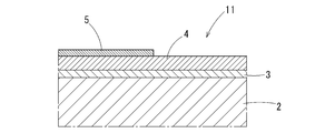
- the terminal material 1 for a connector of the present embodiment is formed on a plate-shaped base material 2 having at least a surface layer made of copper or a copper alloy and an upper surface of the base material 2, as schematically shown in FIG. It includes a nickel plating layer 3 made of nickel or a nickel alloy, and a silver-nickel alloy plating layer 4 formed on the upper surface of the nickel plating layer 3.
- the composition of the surface layer of the base material 2 is not particularly limited as long as it is made of copper or a copper alloy.
- the base material 2 is made of a plate material made of copper or a copper alloy such as oxygen-free copper (C10200) or Cu—Mg-based copper alloy (C18665). It may be composed of a plating material in which the surface of a base material that is not a copper alloy is plated with copper or copper alloy. In this case, a metal plate other than copper can be applied as the base material.
- the nickel plating layer 3 is formed by subjecting the base material 2 to a nickel plating treatment made of nickel or a nickel alloy, and coats the base material 2.
- the nickel plating layer 3 has a function of suppressing the diffusion of copper from the base material 2 into the silver-nickel alloy plating layer 4 that coats the nickel plating layer 3.
- the thickness (thickness) of the nickel plating layer 3 is preferably 0.2 ⁇ m or more and 5.0 ⁇ m or less, and more preferably 0.3 ⁇ m or more and 2.0 ⁇ m or less.
- the thickness of the nickel plating layer 3 is less than 0.2 ⁇ m, copper diffuses from the base material 2 into the silver nickel alloy plating layer 4 under a high temperature environment, and the contact resistance value of the silver nickel alloy plating layer 4 increases. , Heat resistance may decrease.
- the thickness of the nickel plating layer 3 exceeds 5.0 ⁇ m, cracks may occur during bending.
- the composition of the nickel plating layer 3 is not particularly limited as long as it is made of nickel or a nickel alloy.
- the silver-nickel alloy plating layer 4 is formed by subjecting the nickel plating layer 3 to a silver strike plating treatment and then a silver-nickel alloy plating treatment as described later.
- the silver-nickel alloy plating layer 4 is formed on the surface of the connector terminal material 1 with an alloy of silver and nickel. Since no intermetallic compound is generated between silver and nickel, it is possible to prevent the surface hardness of the connector terminal material 1 from becoming too high.
- the nickel content of the silver-nickel alloy plating layer 4 is 0.03 at% or more and 1.20 at% or less, and more preferably 0.03 at% or more and 1.00 at% or less.
- the nickel content of the silver-nickel alloy plating layer 4 is less than 0.03 at%, the heat resistance is lowered and the hardness of the silver-nickel alloy plating layer is lowered, so that the friction coefficient is increased and the abrasion resistance is lowered. To do. If the nickel content of the silver-nickel alloy plating layer 4 exceeds 1.20 at%, the silver-nickel alloy plating layer 4 becomes too hard and cracks are likely to occur due to press processing or the like, and the conductor resistance of the silver-nickel alloy plating layer 4 increases. However, the contact resistance in a high temperature environment tends to increase.
- the contact resistance of the silver-nickel alloy plating layer 4 increases when the nickel content exceeds 1.20 at%. Since the silver-nickel alloy plating layer 4 contains 0.03 at% or more and 1.20 at% or less of nickel as described above, the surface hardness is increased and the wear resistance is improved. Specifically, the Vickers hardness of the silver-nickel alloy plating layer 4 is in the range of 130 HV to 250 HV.
- Nickel has a higher melting point than antimony, so it is difficult to diffuse even in a high temperature environment, so unlike antimony, it is difficult to concentrate on the outermost surface even in a high temperature environment. Therefore, the increase in contact resistance in a high temperature environment can be suppressed, the crystal grain size can be kept small, the coefficient of friction can be kept low, and the wear resistance can be maintained.
- nickel in the silver-nickel alloy plating layer is slightly co-deposited with 0.03 at% or more and 1.20 at% or less.
- the crystal grain size can be made finer only by itself.
- the silver-nickel alloy plating layer 4 has a fine average crystal grain size of 10 nm or more and 150 nm or less, and contains nickel. Therefore, coarsening of crystal grains is suppressed even when exposed to a high temperature environment, and the high temperature environment. There is little decrease in wear resistance underneath.
- the silver-nickel alloy plating layer is formed, if nickel is not co-deposited or the amount of coagulation is less than 0.03 at%, the average crystal grain size of the silver-nickel alloy plating layer may exceed 150 nm. In this case, since the amount of nickel eutectoid is small and the plating layer has characteristics close to those of sterling silver, the crystal grains may become coarse in a high temperature environment and the wear resistance may decrease. It is preferable that the average crystal grain size is small, but when measuring crystal grains of less than 10 nm, the reliability of the measurement result is low and it is not realistic.
- the average crystal grain size is preferably 100 nm or less.
- a plate material whose surface layer is at least made of copper or a copper alloy is prepared, and the surface is cleaned by degreasing, pickling, or the like.
- Silver strike plating process After the activation treatment is performed on the nickel plating layer 3 with a 5 to 10% by mass potassium cyanide aqueous solution, a silver strike plating treatment is performed on the nickel plating layer 3 for a short time to form a thin silver plating layer.
- the composition of the silver plating bath for performing this silver strike plating treatment is not particularly limited, and includes, for example, silver cyanide (AgCN) 1 g / L to 5 g / L and potassium cyanide (KCN) 80 g / L to 120 g / L. ..
- a silver strike plating layer is formed by performing a silver strike plating treatment for about 30 seconds under the conditions of a bath temperature of 25 ° C. and a current density of 1 A / dm 2 using stainless steel (SUS316) as an anode for this silver plating bath. It is formed.
- the silver strike plating layer is subsequently formed with the silver-nickel alloy plating layer 4, which makes it difficult to identify the silver strike plating layer as a layer.
- the plating bath for forming the silver-nickel alloy plating layer 4 is, for example, silver cyanide (AgCN) 30 g / L to 50 g / L, potassium cyanide (KCN) 100 g / L to 150 g / L, potassium carbonate (K 2 CO 3). ) 15 g / L to 40 g / L, potassium tetracyanonickel (II), monohydrate (K 2 [Ni (CN) 4 ], H 2 O) 80 g / L to 150 g / L, and a silver-plated layer.
- a cyanide bath having a composition consisting of additives for smooth precipitation can be used.
- This additive may be a general additive as long as it does not contain antimony.
- silver cyanide is A mol
- potassium tetracyanonickel (II) acid / monohydrate is B mol
- the molar ratio (A: B) is (3-4) :( 5-6), A + B. It may be adjusted so as to be 0.7 mol to 1.0 mol.
- the film thickness is 0.5 ⁇ m or more.
- a silver-nickel alloy plating layer 4 of 0 ⁇ m or less is formed.
- the plating bath for forming the silver-nickel alloy plating layer 4 is not limited to the above composition, and the composition is not particularly limited as long as it is a cyan bath and the additive does not contain antimony.
- the connector terminal material 1 in which the nickel plating layer 3 and the silver-nickel alloy plating layer 4 are formed on the surface of the base material 2 is formed. Then, by performing press working or the like on the connector terminal material 1, a connector terminal having a silver-nickel alloy plating layer 4 on the surface is formed.
- the silver-nickel alloy plating layer 4 formed on the outermost surface of the base material 2 contains nickel, the hardness of the outermost surface of the base material 2 is increased and the abrasion resistance is improved. Can be improved. Since no intermetallic compound is formed between silver and nickel, it is possible to prevent the outermost surface of the base material 2 from becoming too hard.
- Nickel has a higher melting point than antimony, so heat resistance can be improved and the decrease in hardness can be suppressed. Since the difference in atomic radius between silver and nickel is larger than the difference in atomic radius between silver and antimony, nickel is only slightly co-deposited in the silver-nickel alloy plating layer 4 to 0.03 at% or more and 1.20 at% or less. Therefore, the hardness can be surely increased.
- the nickel plating layer 3 and the silver-nickel alloy plating layer 4 are formed on the entire upper surface of the base material 2, but the present invention is not limited to this, and for example, nickel plating is performed on a part of the upper surface of the base material 2.
- a layer 3 may be formed, and a silver-nickel alloy plating layer 4 may be formed on the nickel plating layer 3, or a part of the upper surface of the nickel plating layer 3 formed on the entire upper surface of the base material 2 may be formed.
- the silver-nickel alloy plating layer 4 may be formed.
- the surface of at least the contact point when formed on the terminal may be the silver-nickel alloy plating layer 4.
- the outermost surface of the terminal material 1 for the connector is composed of the silver-nickel alloy plating layer 4, but as shown in FIG. 2, the silver plating layer 5 is further formed on the silver-nickel alloy plating layer 4. It may be formed.
- the surface of the silver-plated layer 5 is less likely to oxidize even in a high-temperature environment, and an increase in contact resistance can be suppressed.
- the silver-plated layer 5 is made of sterling silver having a purity of 99% by mass or more, preferably 99.9% by mass or more, excluding gas components such as C, H, S, O, and N.
- the purity is set to 99% by mass or more because if the Ag concentration of the silver plating layer 5 is less than 99% by mass, a large amount of impurities are contained and the contact resistance tends to be high.
- "Excluding gas components such as C, H, S, O, and N" is intended to exclude elements of gas components.
- the film thickness of the silver plating layer 5 is preferably 0.01 ⁇ m or more and 2.0 ⁇ m or less. If the film thickness of the silver plating layer 5 is less than 0.01 ⁇ m, it is too thin, so that it easily wears and disappears at an early stage. If the film thickness exceeds 2.0 ⁇ m, the soft silver plating layer 5 becomes thick, so that the friction coefficient may increase.
- the silver plating layer 5 is formed only on a part of the silver-nickel alloy plating layer 4, specifically, a portion that becomes a contact point when the terminal is processed.
- the composition of the silver plating bath for forming the silver plating layer 5 is not particularly limited, but for example, silver potassium cyanide (K [Ag (CN) 2 ]) 45 g / L to 55 g / L, potassium cyanide (KCN) 110 g. It consists of / L to 130 g / L, potassium carbonate (K 2 CO 3 ) 10 g / L to 20 g / L, and additives.
- a pure silver plate is used as an anode for this silver plating bath, and the plating treatment is performed at a bath temperature of room temperature (25 ° C to 30 ° C) and a current density of 2A / dm 2 to 4A / dm 2 .
- the silver plating layer 5 is formed.
- a base material having a thickness of 0.3 mm made of a copper alloy plate was prepared, and the surface of the base material was subjected to pretreatment to clean the surface by degreasing, pickling, etc. (pretreatment step).
- pretreatment step was subjected to a nickel plating treatment to form a nickel plating layer having a thickness of 1 ⁇ m (nickel plating layer forming step).
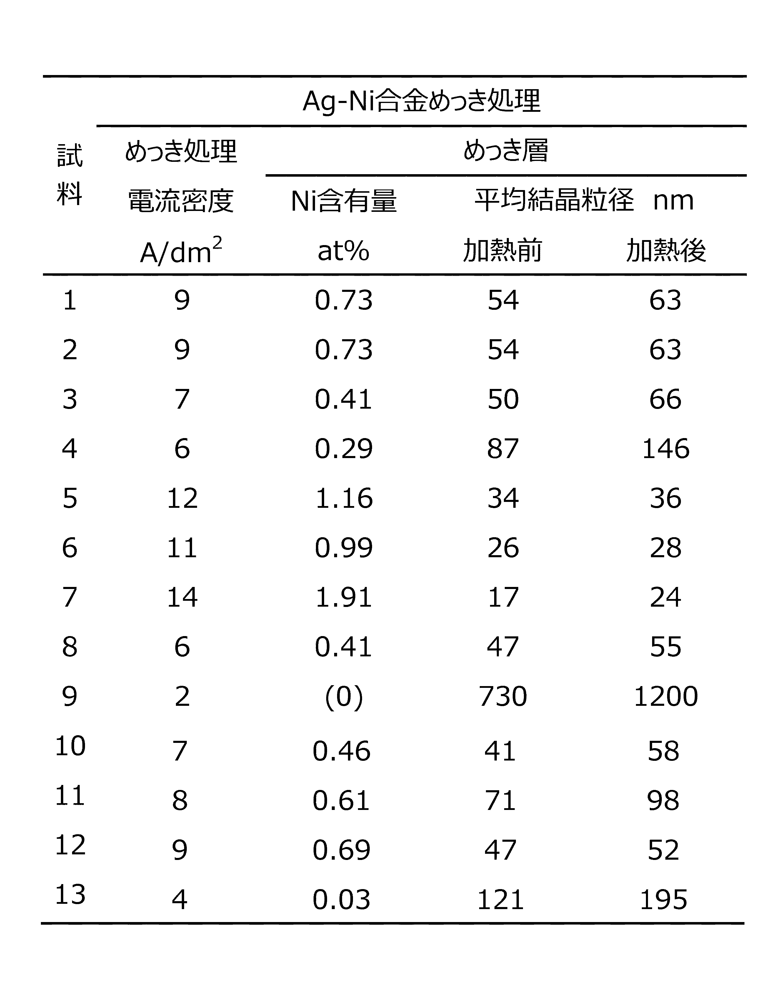
- a silver-nickel alloy plating treatment is performed on the silver-nickel alloy plating layer (silver-nickel alloy plating layer forming step) to prepare a sample in which a silver-nickel alloy plating layer having the film thickness, nickel content, and average crystal grain size shown in Tables 1 and 2 is formed. did.
- nickel is described as Ni
- silver-nickel alloy is described as Ag—Ni alloy
- silver is described as Ag.
- the average crystal grain size in the silver-nickel alloy plating layer is simply described as the average crystal grain size.
- the nickel content in the silver-nickel alloy plating layer was adjusted by the current density of the plating treatment.
- Nickel sulfamate 300 g / L Nickel chloride / hexahydrate: 30 g / L Boric acid: 30 g / L ⁇ Bath temperature: 45 ° C -Current density: 3A / dm 2
- the thickness of the plating layer formed by the silver-nickel alloy plating treatment, the nickel content in the plating layer, the average crystal grain size of the plating layer, and the thickness of the plating layer formed by the silver plating treatment were measured.
- the presence or absence of cracks after indentation, contact resistance before and after heating, and wear resistance were measured.
- the film thickness of the plating layer formed by the silver-nickel alloy plating treatment and the silver plating treatment was measured as follows. Focused ion beam device manufactured by Seiko Instruments Co., Ltd .: Cross-section processing is performed on each sample using FIB (model number: SMI3050TB), and the film thickness at any three locations in the cross-section SIM (Scanning Ion Microscope) image with an inclination angle of 60 °. Was measured, the average was calculated, and then converted to the actual length. The measurement results are shown in Table 1. As shown in Table 1, the film thickness of the nickel plating layer formed by the nickel plating treatment was 1 ⁇ m for all the samples.
- the obtained crystal grain size was approximated to an area circle, and the average crystal grain size was calculated by a weighted average weighted by the area.
- Table 2 shows the results measured before and after heating at 150 ° C. for 240 hours.
- the equipment and analysis software used to measure the average crystal grain size of the silver-nickel alloy plating layers of Samples 1 to 8, 10 to 13 are as follows.
- EBSD device EDAX / TSL
- OIM Data Collection Analysis software OIM Data Analysis ver. Made by EDAX / TSL. 5.2
- a cross section along the growth direction of electrodeposition of the plating film (the thickness direction of the base material) is processed by the ion milling method, and a field emission scanning electron microscope (Field Measurement Scanning Electron Microscope: FE-SEM) with an EBSD device is used. Then, the measurement is performed in a measurement range of 3500 ⁇ m ⁇ 1000 nm and a measurement step of 0.04 ⁇ m, analyzed using this data and analysis software, and the grain boundary is defined as the interval between measurement points where the orientation difference between adjacent measurement points is 5 ° or more. Assuming, the grain size (including twin crystals) was measured.
- FE-SEM Field Measurement Scanning Electron Microscope
- the obtained crystal grain size was approximated to an area circle, and the average crystal grain size was calculated by a weighted average weighted by the area.
- Table 2 shows the results measured before and after heating at 150 ° C. for 240 hours.
- the equipment and analysis software used to measure the average crystal grain size in the plating layer of Sample 9 are as follows.
- EBSD device EDAX / TSL OIM Data Collection
- FE-SEM JSM-7001FA manufactured by JEOL Ltd.
- Analysis software OIM Data Analysis ver. Made by EDAX / TSL. 5.2
- the sample was cut out from an arbitrary place, and the element distribution was measured while sputtering from the surface in the depth direction.
- the measurement area had a diameter of 4 mm, and elements having an atomic number of 27 or less were excluded.
- Ultra-high purity Ar gas was used for the measurement, the gas pressure was 600 Pa, the high frequency output was 35 W, the pulse frequency was 1000 Hz, the duty cycle was 0.25 (25% discharge), and the uptake interval was 0.01 s.
- the nickel content (at%) in the plating layer was determined by converting the film thickness of the plating layer into a composition (at%) using a judgment amount kit from the element distribution at the time of sputtering of about 0.2 ⁇ m. The measurement results are shown in Table 2.
- the nickel content (at%) of the plating layer can also be measured using, for example, an electron probe microanalyzer manufactured by JEOL Ltd .: EPMA (model number JXA-8530F).
- EPMA model number JXA-8530F
- the contact resistance (m ⁇ ) of each of these test pieces was measured before heating and after heating at 150 ° C. for 240 hours.
- a friction and wear tester UMT-Tribolab manufactured by Bruker AXS Co., Ltd. was used to bring the convex surface of the convex part of the female terminal test piece into contact with the horizontally installed male terminal test piece and apply a load of 10 N.
- the contact resistance value of the male terminal test piece when it was applied was measured by the 4-terminal method. The measurement results are shown in Table 3. The contact resistance was not measured for samples with cracks due to indentation.
- test pieces ⁇ and ⁇ having the same shape as the test pieces used for measuring the contact resistance were prepared. Whether or not one of the underlying nickel plating layers was exposed after the convex surface of the convex portion of the test piece ⁇ and the test piece ⁇ were pressed against each other with a load of 5 N and slid 50 times repeatedly at a distance of 5 mm. was observed using SEM-EDS (scanning electron microscope). Observing both the flat plate side and the convex side, if more than half of the sliding part was exposed, "C”, if less than half was exposed, "B”, completely exposed. The one in which was not recognized was designated as "A”. The measurement results are shown in Table 3.
- Samples 1 to 6, 8, 12, and 13 have no cracks after indentation, and the contact resistance value is small before and after heating (240 hours at 150 ° C.) and has high heat resistance. Was shown.
- the samples 2 to 6 and 8 on which the silver-plated layer is formed have a particularly low contact resistance before heating, and the low contact resistance is maintained even after heating, so that the heat resistance can be improved. It can also be seen that it is also excellent in wear resistance.
- sample 13 Since sample 13 has a low nickel content in the silver-nickel alloy plating layer, contact resistance similar to that of samples 2 to 6 and 8 on which the silver plating layer is formed is obtained, but silver-nickel alloy plating after heating is obtained.
- the crystal grain size of the layer is slightly larger.
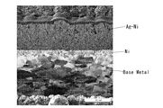
- FIG. 3 is a cross-sectional SIM image of sample 1, in which a silver-nickel alloy plating layer (denoted as Ag-Ni) is formed on a nickel plating layer (denoted as Ni) on the surface of a base material (denoted as Base Material). It is shown that
- FIG. 4 is a cross-sectional SIM image of Sample 1 after heating (at 150 ° C. for 240 hours), showing that the average crystal grain size of the silver-nickel alloy plating layer is small even after heating and is maintained in a fine state. Has been done.
- Sample 7 had a high nickel content in the silver-nickel alloy plating layer, and the surface of the plating layer had large irregularities. That is, since the precipitated crystal grains are coarse due to the high nickel content and the plating solution is involved at the time of precipitation, there are many impurities, and these impurities and nickel are oxidized by heating, and the contact resistance is increased.
- the film thickness of the silver-nickel alloy plating layer was as small as 0.3 ⁇ m, and the underlying nickel plating layer was significantly exposed in the abrasion resistance test.
- the wear resistance and heat resistance of the terminal material for the connector can be improved.
Landscapes
- Chemical & Material Sciences (AREA)
- Engineering & Computer Science (AREA)
- Materials Engineering (AREA)
- Metallurgy (AREA)
- Organic Chemistry (AREA)
- Mechanical Engineering (AREA)
- Chemical Kinetics & Catalysis (AREA)
- Electrochemistry (AREA)
- Electroplating Methods And Accessories (AREA)
Abstract
少なくとも表層が銅又は銅合金からなる基材と、その基材の表面を被覆するニッケル又はニッケル合金からなるニッケルめっき層と、ニッケルめっき層の上の少なくとも一部に形成され、膜厚が0.5μm以上20μm以下、ニッケル含有量が0.03at%以上1.20at%以下、平均結晶粒径が10nm以上150nm以下である銀ニッケル合金めっき層と、を備えており、耐摩耗性及び耐熱性を向上できるコネクタ用端子材を提供する。
Description
本発明は、高電流、高電圧が印加される自動車や民生機器等の電気配線の接続に使用される有用な皮膜が設けられたコネクタ用端子材に関する。本願は、2019年8月9日に日本国に出願された特願2019-146951号及び2020年4月27日に日本国に出願された特願2020-078202号に基づき優先権を主張し、その内容をここに援用する。
従来、自動車等の電気配線の接続に用いられる車載用コネクタが知られている。車載用コネクタ(車載用端子)は、メス端子に設けられた接触片とメス端子内に挿入されたオス端子とが所定の接触圧で接触することで、電気的に接続されるように設計された端子対を備える。
このようなコネクタ(端子)として、一般的に銅または銅合金板上に錫めっきを施し、リフロー処理を行った錫めっき付き端子が多く用いられていた。しかし、近年、自動車の高電流・高電圧化に伴い、より電流を多く流すことができる耐熱性及び耐摩耗性に優れた貴金属めっきを施した端子の用途が増加している。
このような耐熱性及び耐摩耗性が求められる車載用端子として、例えば、特許文献1に記載のコネクタ用銀めっき端子が知られている。この特許文献1に記載のコネクタ用銀めっき端子は、銅又は銅合金からなる母材の表面が銀めっき層により被覆されている。
この銀めっき層は、下層側(母材側)に位置する第1の銀めっき層と、第1の銀めっき層の上層側に位置する第2の銀めっき層を有し、第1の銀めっき層の結晶粒径が第2の銀めっき層の結晶粒径よりも大きく形成されている。すなわち、特許文献1の構成では、第1の銀めっき層の結晶粒径を第2の銀めっき層の結晶粒径よりも大きく形成することで、母材からの銅が第2の銀めっき層に拡散するのを抑制している。
特許文献2には、母材としての銅又は銅合金部材の表面の少なくとも一部にアンチモン濃度が0.1質量%以下の銀又は銀合金層が形成され、この銀又は銀合金層の上に最表層としてアンチモン濃度が0.5質量%以上のビッカース硬度HV140以上の銀合金層が形成された銅又は銅合金部材が開示されている。すなわち、特許文献2の構成では、アンチモンを銀又は銀合金層に添加することで硬度を上昇させて、銅又は銅合金部材の耐摩耗性を向上させている。
特許文献1の構成では、母材の表面を被覆する銀めっき層は、経時変化および高温環境下での使用によって銀の結晶粒径が大きくなる(粗大化)に伴い硬度が低下するので、長時間の使用および高温環境下での耐摩耗性が低下する。この耐摩耗性の低下を補うために、銀めっき層の膜厚を厚くすることが考えられるが、コスト面での問題がある。特許文献2の構成では、加熱によってアンチモンがめっき層最表面に拡散し、濃化後、酸化して接触抵抗が増大する問題がある。
本発明は、このような事情に鑑みてなされたもので、耐摩耗性及び耐熱性を向上できるコネクタ用端子材を提供することを目的とする。
本発明のコネクタ用端子材は、少なくとも表層が銅又は銅合金からなる基材と、前記基材の表面に被覆されたニッケル又はニッケル合金からなるニッケルめっき層と、前記ニッケルめっき層の上の少なくとも一部に形成され、膜厚が0.5μm以上20.0μm以下で、ニッケル含有量が0.03at%以上1.20at%以下、平均結晶粒径が10nm以上150nm以下である銀ニッケル合金めっき層と、を備える。
本発明では、表面に形成された銀ニッケル合金めっき層がニッケルを含んでいるので、銀めっき層と比較して平均結晶粒径が小さく、摺動時の凝着現象の発生を抑制するので、摩擦係数が低く、耐摩耗性を向上できる。
この場合、銀ニッケル合金めっき層の平均結晶粒径が10nm以上150nm以下と微細であり、ニッケルを含有していることから、高温環境下にさらされても結晶粒の粗大化が抑制され、高温環境下での耐摩耗性の低下も小さい。銀ニッケル合金めっき層を形成する際に、ニッケルが共析されない、あるいは0.03at%よりも共析量が少ない場合、銀ニッケル合金めっき層の平均結晶粒径が150nmを超えることがある。この場合は、ニッケルの共析量が少なく、純銀の特性に近いめっき層となるため、高温環境下で結晶粒が粗大化して、耐摩耗性が低下するおそれがある。平均結晶粒径は小さい方が好ましいが、10nm未満の結晶粒を測定する場合、測定結果の信頼性が低く現実的でない。
また、ニッケルはアンチモンに比べて融点が高いので、高温環境下でも拡散しがたく、このため、アンチモンと異なり、高温環境下でも最表面に濃化しがたい。これにより、高温環境下での接触抵抗の増大を抑え、結晶粒径を小さいまま保つことができ、摩擦係数を低く維持し、耐摩耗性を保持することができる。
銀とニッケルとの原子半径差は、銀とアンチモンとの原子半径差に比べて大きいため、銀ニッケル合金めっき層内におけるニッケル含有量を0.03at%以上1.20at%以下として、ニッケルを僅かに共析させるだけで結晶粒径を微細にすることができる。
銀ニッケル合金めっき層のニッケル含有量が0.03at%未満であると、耐熱性及び耐摩耗性が低下し、摩擦係数も増大する。ニッケル含有量が1.20at%を超えると銀ニッケル合金めっき層の導体抵抗が増大し、また、高温環境下での接触抵抗も増大しやすくなる。
銀ニッケル合金めっき層の膜厚が0.5μm未満であると、耐熱性及び耐摩耗性を向上できず、20.0μmを超えると、銀ニッケル合金めっき層が厚すぎてプレス加工等により割れが生じる。
コネクタ用端子材の他の一つの態様としては、前記銀ニッケル合金めっき層の上に、ガス成分であるC、H、S、O、Nを除く銀の純度が99質量%以上、膜厚0.01μm以上2.0μm以下の銀めっき層をさらに備えていてもよい。
表面に比較的軟らかい銀めっき層が形成されるので、その潤滑効果により、耐摩耗性が向上する。銀めっき層は、膜厚が0.01μm未満では薄すぎるため、耐摩耗性向上の効果に乏しく、早期に摩耗して消失し易い。2.0μmを超える厚さでは、軟らかい銀めっき層が厚いため、摩擦係数が増大する傾向にある。「ガス成分であるC、H、S、O、Nを除く」とは、ガス成分の元素を除外する趣旨である。
コネクタ用端子材のさらに他の一つの態様としては、前記ニッケルめっき層の膜厚は0.2μm以上5.0μm以下であるとよい。
ニッケルめっき層の膜厚が0.2μm未満であると、高温環境下では銅又は銅合金からなる基材から銅が銀ニッケル合金めっき層内に拡散する。銀ニッケル合金めっき層内に拡散した銅がめっき膜の最表面まで拡散すると、銅が酸化して接触抵抗が大きくなり、耐熱性が低下する可能性がある。一方、ニッケルめっき層の膜厚が5.0μmを超えると、曲げ加工時等に割れが発生する可能性がある。ニッケルめっき層のより好ましい膜厚は0.3μm以上2.0μm以下である。
本発明によれば、コネクタ用端子材の耐摩耗性及び耐熱性を向上できる。
以下、本発明の実施形態について図面を用いて説明する。
[コネクタ用端子材の構成]
本実施形態のコネクタ用端子材1は、図1に断面を模式的に示したように、少なくとも表層が銅又は銅合金からなる板状の基材2と、基材2の上面に形成されたニッケル又はニッケル合金からなるニッケルめっき層3と、ニッケルめっき層3の上面に形成された銀ニッケル合金めっき層4と、を備えている。
本実施形態のコネクタ用端子材1は、図1に断面を模式的に示したように、少なくとも表層が銅又は銅合金からなる板状の基材2と、基材2の上面に形成されたニッケル又はニッケル合金からなるニッケルめっき層3と、ニッケルめっき層3の上面に形成された銀ニッケル合金めっき層4と、を備えている。
基材2の表層は、銅または銅合金からなるものであれば、特に、その組成が限定されるものではない。本実施形態では、図1に示すように、基材2は無酸素銅(C10200)やCu-Mg系銅合金(C18665)等の銅又は銅合金からなる板材により構成されているが、銅または銅合金ではない母材の表面に銅めっき又は銅合金めっきが施されためっき材により構成されてもよい。この場合、母材としては、銅以外の金属板を適用できる。
ニッケルめっき層3は、基材2上にニッケル又はニッケル合金からなるニッケルめっき処理を施すことにより形成され、基材2を被覆する。ニッケルめっき層3は、ニッケルめっき層3を被覆する銀ニッケル合金めっき層4への基材2からの銅の拡散を抑制する機能を有する。
ニッケルめっき層3の厚さ(膜厚)は、0.2μm以上5.0μm以下であることが好ましく、より好ましくは0.3μm以上2.0μm以下であるとよい。ニッケルめっき層3の厚さが0.2μm未満であると、高温環境下では基材2から銅が銀ニッケル合金めっき層4内に拡散して銀ニッケル合金めっき層4の接触抵抗値が大きくなり、耐熱性が低下する可能性がある。一方、ニッケルめっき層3の厚さが5.0μmを超えると、曲げ加工時に割れが発生する可能性がある。なお、ニッケルめっき層3は、ニッケル又はニッケル合金からなるものであれば、特に、その組成が限定されるものではない。
銀ニッケル合金めっき層4は、後述するようにニッケルめっき層3の上に銀ストライクめっき処理を施した後に銀ニッケル合金めっき処理を施すことにより形成される。銀ニッケル合金めっき層4は、コネクタ用端子材1の表面に、銀とニッケルとの合金により形成される。銀とニッケルとの間には金属間化合物が生成されないので、コネクタ用端子材1の表面の硬度が高くなりすぎることを抑制している。
銀ニッケル合金めっき層4のニッケル含有量は、0.03at%以上1.20at%以下とされ、より好ましくは0.03at%以上1.00at%以下であるとよい。銀ニッケル合金めっき層4のニッケル含有量が0.03at%未満であると、耐熱性が低下するとともに、銀ニッケル合金めっき層の硬さが低下するため、摩擦係数が増大及び耐摩耗性が低下する。銀ニッケル合金めっき層4のニッケル含有量が1.20at%を超えると銀ニッケル合金めっき層4が硬くなりすぎて、プレス加工等により割れが生じ易く、銀ニッケル合金めっき層4の導体抵抗が増大し、高温環境下での接触抵抗も増大しやすくなる。
ニッケルは銀よりも電気伝導率が低いので、ニッケル含有量が1.20at%を超えると銀ニッケル合金めっき層4の接触抵抗が高くなる。銀ニッケル合金めっき層4は、上述したように0.03at%以上1.20at%以下のニッケルを含んでいるため、表面の硬度が高められ、耐摩耗性が向上する。具体的には、銀ニッケル合金めっき層4のビッカース硬さは、130HV~250HVの範囲内となる。
ニッケルはアンチモンに比べて融点が高いので、高温環境下でも拡散しがたいため、アンチモンと異なり、高温環境下でも最表面に濃化しがたい。このため、高温環境下での接触抵抗の増大を抑え、結晶粒径を小さいまま保つことができ、摩擦係数を低く維持し、耐摩耗性を保持できる。
銀とニッケルとの原子半径差は、銀とアンチモンとの原子半径差に比べて大きいため、銀ニッケル合金めっき層内におけるニッケルを0.03at%以上1.20at%以下と、僅かに共析させるだけで、結晶粒径を微細にすることができる。
銀ニッケル合金めっき層4は、平均結晶粒径が10nm以上150nm以下と微細であり、ニッケルを含有していることから、高温環境下にさらされても結晶粒の粗大化が抑制され、高温環境下での耐摩耗性の低下も少ない。銀ニッケル合金めっき層を形成する際に、ニッケルが共析されない、あるいは0.03at%よりも共析量が少ない場合、銀ニッケル合金めっき層の平均結晶粒径が150nmを超えることがある。この場合は、ニッケルの共析量が少なく、純銀の特性に近いめっき層となるため、高温環境下で結晶粒が粗大化して、耐摩耗性が低下するおそれがある。平均結晶粒径は小さい方が好ましいが、10nm未満の結晶粒を測定する場合、測定結果の信頼性が低く現実的でない。この平均結晶粒径は好ましくは100nm以下である。
銀ニッケル合金めっき層4の膜厚は、0.5μm以上20.0μm以下に設定され、より好ましくは1.0μm以上10.0μm以下である。銀ニッケル合金めっき層4の膜厚が0.5μm未満であると、耐熱性及び耐摩耗性を向上できず、20.0μmを超えると、銀ニッケル合金めっき層4が厚すぎて、プレス加工等により割れが生じる。
次に、このコネクタ用端子材1の製造方法について説明する。コネクタ用端子材1の製造方法は、基材2となる少なくとも表層が銅又は銅合金からなる板材を洗浄する前処理工程と、ニッケルめっき層3を基材2に形成するニッケルめっき層形成工程と、ニッケルめっき層3上に銀ストライクめっき処理を施す銀ストライクめっき工程と、銀ストライクめっき処理の後に銀ニッケル合金めっき処理を施して銀ニッケル合金めっき層4を形成する銀ニッケル合金めっき層形成工程と、を備える。
[前処理工程]
まず、基材2として、少なくとも表層が銅又は銅合金からなる板材を用意し、この板材を脱脂、酸洗等をすることによって表面を清浄する前処理を行う。
まず、基材2として、少なくとも表層が銅又は銅合金からなる板材を用意し、この板材を脱脂、酸洗等をすることによって表面を清浄する前処理を行う。
[ニッケルめっき層形成工程]
前処理を施した基材2の表面の少なくとも一部に対して、ニッケル又はニッケル合金からなるめっき皮膜を形成するめっき処理を施して、ニッケルめっき層3を基材2に形成する。具体的には例えば、スルファミン酸ニッケル300g/L、塩化ニッケル・六水和物30g/L、ホウ酸30g/Lを含むニッケルめっき浴を用いて、浴温45℃、電流密度3A/dm2の条件下でニッケルめっき処理を施す。なお、ニッケルめっき層3を形成するニッケルめっき処理は、緻密なニッケル主体の膜が得られるものであれば特に限定されず、公知のワット浴を用いる電気めっき処理であってもよい。
前処理を施した基材2の表面の少なくとも一部に対して、ニッケル又はニッケル合金からなるめっき皮膜を形成するめっき処理を施して、ニッケルめっき層3を基材2に形成する。具体的には例えば、スルファミン酸ニッケル300g/L、塩化ニッケル・六水和物30g/L、ホウ酸30g/Lを含むニッケルめっき浴を用いて、浴温45℃、電流密度3A/dm2の条件下でニッケルめっき処理を施す。なお、ニッケルめっき層3を形成するニッケルめっき処理は、緻密なニッケル主体の膜が得られるものであれば特に限定されず、公知のワット浴を用いる電気めっき処理であってもよい。
[銀ストライクめっき工程]
ニッケルめっき層3に対して5~10質量%のシアン化カリウム水溶液を用いて活性化処理を行った後、ニッケルめっき層3上に銀ストライクめっき処理を短時間施して薄い銀めっき層を形成する。
ニッケルめっき層3に対して5~10質量%のシアン化カリウム水溶液を用いて活性化処理を行った後、ニッケルめっき層3上に銀ストライクめっき処理を短時間施して薄い銀めっき層を形成する。
この銀ストライクめっき処理を施すための銀めっき浴の組成は、特に限定されないが、例えば、シアン化銀(AgCN)1g/L~5g/L、シアン化カリウム(KCN)80g/L~120g/Lからなる。この銀めっき浴に対してアノードとしてステンレス鋼(SUS316)を用いて、浴温25℃、電流密度1A/dm2の条件下で銀ストライクめっき処理を30秒程度施すことにより、銀ストライクめっき層が形成される。この銀ストライクめっき層は、その後に銀ニッケル合金めっき層4が形成されることにより、層としての識別は困難になる。
[銀ニッケル合金めっき層形成工程]
銀ストライクめっき処理後に銀ニッケル合金めっき処理を施して、銀ニッケル合金めっき層4を形成する。銀ニッケル合金めっき層4を形成するためのめっき浴は、例えば、シアン化銀(AgCN)30g/L~50g/L、シアン化カリウム(KCN)100g/L~150g/L、炭酸カリウム(K2CO3)15g/L~40g/L、テトラシアノニッケル(II)酸カリウム・一水和物(K2[Ni(CN)4]・H2O)80g/L~150g/L、および銀めっき層を平滑に析出させるための添加剤からなる組成のシアン浴を利用できる。
銀ストライクめっき処理後に銀ニッケル合金めっき処理を施して、銀ニッケル合金めっき層4を形成する。銀ニッケル合金めっき層4を形成するためのめっき浴は、例えば、シアン化銀(AgCN)30g/L~50g/L、シアン化カリウム(KCN)100g/L~150g/L、炭酸カリウム(K2CO3)15g/L~40g/L、テトラシアノニッケル(II)酸カリウム・一水和物(K2[Ni(CN)4]・H2O)80g/L~150g/L、および銀めっき層を平滑に析出させるための添加剤からなる組成のシアン浴を利用できる。
この添加剤は、アンチモンを含まないものであれば、一般的な添加剤で構わない。なお、シアン化銀をAモル、テトラシアノニッケル(II)酸カリウム・一水和物をBモルとしたときのモル比(A:B)が(3~4):(5~6)、A+B=0.7モル~1.0モルとなるように調整するとよい。
このめっき浴に対してアノードとして純銀板を用いて、浴温25℃、電流密度4A/dm2~12A/dm2の条件下で銀ニッケル合金めっきを施すことにより膜厚0.5μm以上20.0μm以下の銀ニッケル合金めっき層4が形成される。
銀ニッケル合金めっき処理の電流密度が4A/dm2未満であると、ニッケルの共析が妨げられ、電流密度が12A/dm2を超えると、銀ニッケル合金めっき層4の外観が損なわれる。銀ニッケル合金めっき層4を形成するためのめっき浴は、上記組成に限定されず、シアン浴であり、かつ添加剤にアンチモンが含まれていなければ、その組成は特に限定されない。
このようにして基材2の表面にニッケルめっき層3及び銀ニッケル合金めっき層4が形成されたコネクタ用端子材1が形成される。そして、コネクタ用端子材1に対してプレス加工等を施すことにより、表面に銀ニッケル合金めっき層4を備えるコネクタ用端子が形成される。
本実施形態のコネクタ用端子材1は、基材2の最表面に形成された銀ニッケル合金めっき層4がニッケルを含んでいるので、基材2の最表面の硬度を高め、耐摩耗性を向上できる。銀とニッケルとの間には金属間化合物が生成されないので、基材2の最表面の硬度が高くなりすぎることを抑制できる。
ニッケルはアンチモンに比べて融点が高いので、耐熱性を向上でき、硬度が低下することを抑制できる。銀とニッケルとの原子半径差が銀とアンチモンとの原子半径差に比べて大きいため、銀ニッケル合金めっき層4内においてニッケルを0.03at%以上1.20at%以下と僅かに共析させるだけで、硬度を確実に上昇させることができる。
その他、細部構成は実施形態の構成のものに限定されるものではなく、本発明の趣旨を逸脱しない範囲において種々の変更を加えることが可能である。例えば、上記実施形態では、基材2の上面全域にニッケルめっき層3及び銀ニッケル合金めっき層4が形成されているが、これに限らず、例えば、基材2の上面の一部にニッケルめっき層3が形成され、そのニッケルめっき層3の上に銀ニッケル合金めっき層4が形成されていてもよいし、基材2の上面の全域に形成したニッケルめっき層3の上面の一部に、銀ニッケル合金めっき層4が形成されていてもよい。端子に形成された際に少なくとも接点となる部分の表面が銀ニッケル合金めっき層4であればよい。
さらに、前述の実施形態では、コネクタ用端子材1の最表面を銀ニッケル合金めっき層4により構成したが、図2に示すように、銀ニッケル合金めっき層4の上にさらに銀めっき層5を形成してもよい。
銀めっき層5は、高温環境下においても表面が酸化しにくく、接触抵抗の増大を抑制できる。銀めっき層5は、C、H、S、O、Nなどのガス成分を除く純度が99質量%以上、好ましくは99.9質量%以上の純銀からなる。純度が99質量%以上としたのは、銀めっき層5のAg濃度が99質量%未満であると不純物が多く含まれ、接触抵抗が高くなる傾向にあるからである。「C、H、S、O、Nなどのガス成分を除く」とは、ガス成分の元素を除外する趣旨である。
銀めっき層5は、比較的軟質であるが、その下の硬い銀ニッケル合金めっき層4により支持されるので、潤滑効果に優れ、耐摩耗性が向上する。銀めっき層5の膜厚は0.01μm以上2.0μm以下が好ましい。銀めっき層5の膜厚が0.01μm未満では薄すぎるため、早期に摩耗して消失し易い。2.0μmを超える膜厚では、軟らかい銀めっき層5が厚くなるため、摩擦係数が増大するおそれがある。
図2に示す例では、銀めっき層5は、銀ニッケル合金めっき層4の一部、具体的には、端子に加工したときに接点となる部分にのみ形成されている。
銀めっき層5を形成するための銀めっき浴の組成は、特に限定されないが、例えば、シアン化銀カリウム(K[Ag(CN)2])45g/L~55g/L、シアン化カリウム(KCN)110g/L~130g/L、炭酸カリウム(K2CO3)10g/L~20g/L、添加剤からなる。この銀めっき浴に対してアノードとして純銀板を用いて、浴温が常温(25℃~30℃)で、電流密度2A/dm2~4A/dm2の条件下でめっき処理を施すことにより、銀めっき層5が形成される。
銅合金板からなる厚さ0.3mmの基材を用意し、この基材に脱脂、酸洗等をすることによって表面を清浄する前処理を行った(前処理工程)後、基材の表面にニッケルめっき処理を施して膜厚1μmのニッケルめっき層を形成した(ニッケルめっき層形成工程)。
そして、5質量%のシアン化カリウム水溶液を用いてニッケルめっき表面を清浄化する活性化処理を行った後に、ニッケルめっき層が被覆された基材に対して、銀ストライクめっき処理を施した(銀ストライクめっき工程)。
その上に銀ニッケル合金めっき処理を施し(銀ニッケル合金めっき層形成工程)、表1、表2に示す膜厚、ニッケル含有量、平均結晶粒径の銀ニッケル合金めっき層を形成した試料を作製した。なお、表1、表2では、ニッケルをNi、銀ニッケル合金をAg-Ni合金、銀をAgと記載した。また、銀ニッケル合金めっき層中における平均結晶粒径を単に平均結晶粒径と記載した。銀ニッケル合金めっき層におけるニッケル含有量は、めっき処理の電流密度によって調整した。
なお、試料9については、銀ニッケル合金めっき処理を施したが、めっき処理の電流密度が低かったため、形成されためっき層中にニッケルが検出されなかった。
また、試料2~6,8では、銀ニッケル合金めっき層の上に表1に示す膜厚の銀めっき層を形成した。
各めっきの条件は以下のとおりとした。
<ニッケルめっき条件>
・めっき浴組成
スルファミン酸ニッケル:300g/L
塩化ニッケル・六水和物:30g/L
ホウ酸:30g/L
・浴温:45℃
・電流密度:3A/dm2
<ニッケルめっき条件>
・めっき浴組成
スルファミン酸ニッケル:300g/L
塩化ニッケル・六水和物:30g/L
ホウ酸:30g/L
・浴温:45℃
・電流密度:3A/dm2
<銀ストライクめっき条件>
・めっき浴組成
シアン化銀:2g/L
シアン化カリウム:100g/L
・アノード:SUS316
・浴温:25℃
・電流密度:1A/dm2
・めっき浴組成
シアン化銀:2g/L
シアン化カリウム:100g/L
・アノード:SUS316
・浴温:25℃
・電流密度:1A/dm2
<銀ニッケル合金めっき条件>
・めっき浴組成
シアン化銀:35g/L
シアン化カリウム:120g/L
炭酸カリウム:35g/L
テトラシアノニッケル(II)酸カリウム・一水和物:100g/L
添加剤:5ml/L
・アノード:純銀板
・浴温:25℃
・電流密度:4A/dm2~12A/dm2
ニッケル含有量を電流密度によって調整した。なお、比較のため、この範囲から外れる電流密度を2A/dm2、14A/dm2としたものも作製した。電流密度を2A/dm2とした試料9では、形成されためっき層においてニッケルが検出されなかった。
・めっき浴組成
シアン化銀:35g/L
シアン化カリウム:120g/L
炭酸カリウム:35g/L
テトラシアノニッケル(II)酸カリウム・一水和物:100g/L
添加剤:5ml/L
・アノード:純銀板
・浴温:25℃
・電流密度:4A/dm2~12A/dm2
ニッケル含有量を電流密度によって調整した。なお、比較のため、この範囲から外れる電流密度を2A/dm2、14A/dm2としたものも作製した。電流密度を2A/dm2とした試料9では、形成されためっき層においてニッケルが検出されなかった。
<銀めっき条件>
・めっき浴組成
シアン化銀カリウム:55g/L
シアン化カリウム:130g/L
炭酸カリウム:15g/L
光沢剤(アトテックジャパン株式会社製AgO-56):4ml/L
・浴温:25℃
・電流密度:3A/dm2
・アノード:純銀板
・めっき浴組成
シアン化銀カリウム:55g/L
シアン化カリウム:130g/L
炭酸カリウム:15g/L
光沢剤(アトテックジャパン株式会社製AgO-56):4ml/L
・浴温:25℃
・電流密度:3A/dm2
・アノード:純銀板
各試料について、銀ニッケル合金めっき処理により形成されためっき層の膜厚、めっき層中のニッケル含有量およびめっき層の平均結晶粒径、銀めっき処理により形成されためっき層の膜厚を測定し、インデント加工後の割れの有無、加熱前後の接触抵抗および耐摩耗性を測定した。
[各めっき層の膜厚の測定]
銀ニッケル合金めっき処理及び銀めっき処理により形成されためっき層の膜厚は、以下のように測定した。セイコーインスツル株式会社製の集束イオンビーム装置:FIB(型番:SMI3050TB)を用いて各試料に断面加工を行い、傾斜角60°の断面SIM(Scanning Ion Microscopy)像における任意の3箇所の膜厚を測長し、その平均を求めた後、実際の長さに変換した。測定結果を表1に示す。なお、表1に示すように、ニッケルめっき処理により形成したニッケルめっき層の膜厚は、全ての試料について1μmとした。
銀ニッケル合金めっき処理及び銀めっき処理により形成されためっき層の膜厚は、以下のように測定した。セイコーインスツル株式会社製の集束イオンビーム装置:FIB(型番:SMI3050TB)を用いて各試料に断面加工を行い、傾斜角60°の断面SIM(Scanning Ion Microscopy)像における任意の3箇所の膜厚を測長し、その平均を求めた後、実際の長さに変換した。測定結果を表1に示す。なお、表1に示すように、ニッケルめっき処理により形成したニッケルめっき層の膜厚は、全ての試料について1μmとした。

[めっき層の平均結晶粒径の測定]
試料1~8,10~13について、めっき皮膜の電析の成長方向(基材の板厚方向)に沿った断面をイオンミリング法によって加工し、EBSD装置付き透過型電子顕微鏡(Transmission Electron Microscope:TEM)を用いて、測定範囲200nm×400nm、測定ステップ2nmで測定し、このデータと解析ソフトを用いて解析し、隣接する測定点間の方位差が5°以上となる測定点間を結晶粒界とみなして、銀ニッケル合金めっき処理によるめっき層の結晶粒径(双晶を含む)を測定した。
試料1~8,10~13について、めっき皮膜の電析の成長方向(基材の板厚方向)に沿った断面をイオンミリング法によって加工し、EBSD装置付き透過型電子顕微鏡(Transmission Electron Microscope:TEM)を用いて、測定範囲200nm×400nm、測定ステップ2nmで測定し、このデータと解析ソフトを用いて解析し、隣接する測定点間の方位差が5°以上となる測定点間を結晶粒界とみなして、銀ニッケル合金めっき処理によるめっき層の結晶粒径(双晶を含む)を測定した。
得られた結晶粒径を面積円に近似し、面積で重み付けをした加重平均によって平均結晶粒径を算出した。150℃で240時間加熱の前後に測定した結果を表2に示す。
試料1~8,10~13の銀ニッケル合金めっき層の平均結晶粒径の測定に用いた装置、解析ソフトは次のとおりである。
EBSD装置:EDAX/TSL社製OIM Data Collection
解析ソフト:EDAX/TSL社製OIM Data Analysis ver.5.2
EBSD装置:EDAX/TSL社製OIM Data Collection
解析ソフト:EDAX/TSL社製OIM Data Analysis ver.5.2
試料9については、ニッケルを含有しないため銀ニッケル合金めっき層の平均結晶粒径が大きく、上記方法では測定できず、以下のように測定した。
めっき皮膜の電析の成長方向(基材の板厚方向)に沿った断面をイオンミリング法によって加工し、EBSD装置付き電界放出形走査電子顕微鏡(Field Emission Scanning Electron Microscope:FE-SEM)を用いて、測定範囲3500μm×1000nm、測定ステップ0.04μmで測定し、このデータと解析ソフトを用いて解析し、隣接する測定点間の方位差が5°以上となる測定点間を結晶粒界とみなして、結晶粒径(双晶を含む)を測定した。
得られた結晶粒径を面積円に近似し、面積で重み付けをした加重平均によって平均結晶粒径を算出した。150℃で240時間加熱の前後に測定した結果を表2に示す。
試料9のめっき層における平均結晶粒径の測定に用いた装置、解析ソフトは次のとおりである。
EBSD装置:EDAX/TSL社製OIM Data Collection
FE-SEM:日本電子株式会社製JSM-7001FA
解析ソフト:EDAX/TSL社製OIM Data Analysis ver.5.2
EBSD装置:EDAX/TSL社製OIM Data Collection
FE-SEM:日本電子株式会社製JSM-7001FA
解析ソフト:EDAX/TSL社製OIM Data Analysis ver.5.2
[ニッケル含有量(Ni含有量)の測定]
株式会社堀場製作所製のrf-GD-OES(Glow Discharge Optical Emission Spectroscopy)高周波グロー放電 発光分光装置を用いて、銀ニッケル合金めっき処理により形成されためっき層中のニッケル含有量(at%)を測定した。この方法では、表層(銀ニッケル合金めっき層上)に銀めっき層が形成されていても、銀めっき層を除去しなくても組成を測定することができる。
株式会社堀場製作所製のrf-GD-OES(Glow Discharge Optical Emission Spectroscopy)高周波グロー放電 発光分光装置を用いて、銀ニッケル合金めっき処理により形成されためっき層中のニッケル含有量(at%)を測定した。この方法では、表層(銀ニッケル合金めっき層上)に銀めっき層が形成されていても、銀めっき層を除去しなくても組成を測定することができる。
この場合、試料を任意の場所から切り出し、表面から深さ方向にスパッタしながら元素分布の測定を行った。測定エリアは直径4mmとし、原子番号27以下の元素を除いた。測定には超高純度Arガスを用い、ガス圧力は600Pa、高周波出力は35W、パルス周波数は1000Hz、Duty cycleは0.25(25%放電)、取り込み間隔は0.01sでスパッタを行った。
めっき層中のニッケル含有量(at%)は、めっき層の膜厚を約0.2μmスパッタした時点の元素分布から、判定量キットを用いて組成(at%)に変換して求めた。測定結果を表2に示す。
なお、めっき層のニッケル含有量(at%)は、例えば日本電子株式会社製の電子線マイクロアナライザー:EPMA(型番JXA-8530F)を用いて測定することもできる。しかしながら、めっき層の膜厚が十分に厚くないと、下地のニッケルめっき層中のニッケルも検出してしまい、その分、測定値が大きくなるため、上述したGD-OESによる測定が適切である。
得られた試料について、以下に示すように、インデント加工後の割れの有無を確認するとともに、接触抵抗を測定し、耐摩耗性試験を実施した。
[インデント加工後の割れの有無]
試料に曲率半径3mmの半球状の凸部を形成するインデント加工を施した後、光学顕微鏡で凸部の凸面の頂点部を観察し、割れがないか確認した。50倍の観察で試料に入った亀裂の下からニッケルめっき層が認められたものを割れ有(表中“A”)、認められなかったものを割れ無(表中“C”)とした。測定結果を表3に示す。
試料に曲率半径3mmの半球状の凸部を形成するインデント加工を施した後、光学顕微鏡で凸部の凸面の頂点部を観察し、割れがないか確認した。50倍の観察で試料に入った亀裂の下からニッケルめっき層が認められたものを割れ有(表中“A”)、認められなかったものを割れ無(表中“C”)とした。測定結果を表3に示す。
[接触抵抗の測定]
各試料を、60mm×30mmの試験片αと60mm×10mmの試験片βとに切り出し、平板の試験片αをオス端子の代用(オス端子試験片)とし、平板に曲率半径3mmの半球状の凸部を形成するインデント加工を行った試験片βをメス端子の代用(メス端子試験片)とした。
各試料を、60mm×30mmの試験片αと60mm×10mmの試験片βとに切り出し、平板の試験片αをオス端子の代用(オス端子試験片)とし、平板に曲率半径3mmの半球状の凸部を形成するインデント加工を行った試験片βをメス端子の代用(メス端子試験片)とした。
これらの試験片について、加熱前及び150℃で240時間加熱後に、それぞれ接触抵抗(mΩ)を測定した。測定に際しては、ブルカー・エイエックスエス株式会社の摩擦摩耗試験機(UMT-Tribolab)を用い、水平に設置したオス端子試験片にメス端子試験片の凸部の凸面を接触させ、10Nの荷重をかけた時のオス端子試験片の接触抵抗値を4端子法により測定した。測定結果を表3に示す。接触抵抗の測定は、インデント加工で割れが生じた試料については実施しなかった。
[耐摩耗性試験]
試料2,4,9,10について、接触抵抗の測定に用いた試験片と同じ形状の試験片α、βを用意した。試験片βの凸部の凸面と試験片αとを荷重5Nで相互に押圧して、5mmの距離を繰り返し50回摺動させた後、いずれかの下地のニッケルめっき層が露出したか否かをSEM-EDS(走査型電子顕微鏡)を用いて観察した。平板側、凸部側の両方をそれぞれ観察し、摺動部の半分以上が露出していたものを「C」、半分未満のわずかな部分で露出が認められたものを「B」、全く露出が認められなかったものを「A」とした。測定結果を表3に示す。
試料2,4,9,10について、接触抵抗の測定に用いた試験片と同じ形状の試験片α、βを用意した。試験片βの凸部の凸面と試験片αとを荷重5Nで相互に押圧して、5mmの距離を繰り返し50回摺動させた後、いずれかの下地のニッケルめっき層が露出したか否かをSEM-EDS(走査型電子顕微鏡)を用いて観察した。平板側、凸部側の両方をそれぞれ観察し、摺動部の半分以上が露出していたものを「C」、半分未満のわずかな部分で露出が認められたものを「B」、全く露出が認められなかったものを「A」とした。測定結果を表3に示す。
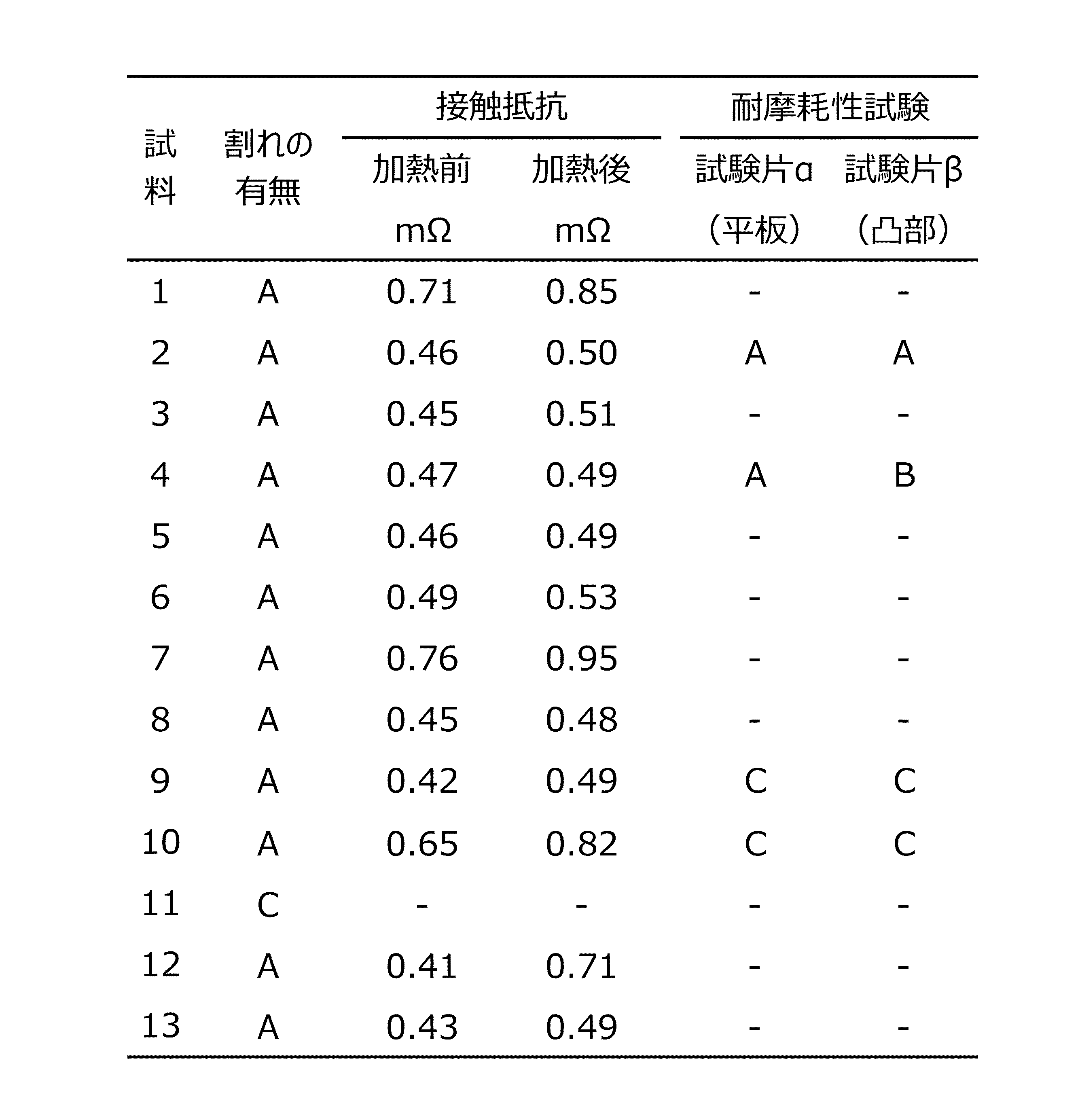
試料1~6,8,12,13は、いずれもインデント加工後の割れが無く、接触抵抗値が加熱前及び加熱後(150℃で240時間)のいずれの場合においても小さく、耐熱性が高いことが示された。
試料1~6,8,12の場合、銀ニッケル合金めっき層の平均結晶粒径は加熱後においても小さく、粗大化が抑制されている。
その中でも、銀めっき層を形成した試料2~6,8は、加熱前の接触抵抗が特に低い値であり、加熱後においても低い接触抵抗が維持されており、耐熱性を向上できる。また、耐摩耗性にも優れることがわかる。
試料13は、銀ニッケル合金めっき層のニッケル含有量が少ないために、銀めっき層を形成した試料2~6,8と同程度の接触抵抗が得られているが、加熱後の銀ニッケル合金めっき層の結晶粒径がやや大きくなっている。
図3は、試料1の断面SIM像であり、基材(Base Materialと表記)表面のニッケルめっき層(Niと表記)の上に、銀ニッケル合金めっき層(Ag‐Niと表記)が形成されていることが示されている。
図4は試料1の加熱後(150℃で240時間)の断面SIM像であり、銀ニッケル合金めっき層の平均結晶粒径が加熱後においても小さく、微細な状態で維持されていることが示されている。
以上の各試料に対して、試料7,9-~11は以下のような不具合が認められた。
試料7は銀ニッケル合金めっき層のニッケル含有量が多く、めっき層表面の凹凸が大きかった。すなわち、ニッケル含有量が多いことにより、析出した結晶粒が粗く、析出時にめっき液を巻き込んでしまうので不純物が多く、この不純物及びニッケルが加熱によって酸化し、接触抵抗が増大した。
試料9は、銀ニッケル合金めっき処理により形成されためっき層においてニッケルが検出されなかった。このため、銀ニッケル合金めっき層の平均結晶粒径が大きく、加熱後においてもさらに粗大化しており、耐摩耗性試験でも下地のニッケルめっき層の露出が認められた。
試料10は、銀ニッケル合金めっき層の膜厚が0.3μmと小さく、耐摩耗性試験で下地のニッケルめっき層が著しく露出した。
試料11は、銀ニッケル合金めっき層の膜厚が28.0μmと大きいため、インデント加工後に割れが認められた。
本発明によれば、コネクタ用端子材の耐摩耗性及び耐熱性を向上できる。
1,11 コネクタ用端子材
2 基材
3 ニッケルめっき層
4 銀ニッケル合金めっき層
5 銀めっき層
2 基材
3 ニッケルめっき層
4 銀ニッケル合金めっき層
5 銀めっき層
Claims (6)
- 少なくとも表層が銅又は銅合金からなる基材と、
前記基材の表面を被覆するニッケル又はニッケル合金からなるニッケルめっき層と、
前記ニッケルめっき層の上の少なくとも一部に形成され、膜厚が0.5μm以上20.0μm以下、ニッケル含有量が0.03at%以上1.20at%以下、平均結晶粒径が10nm以上150nm以下である銀ニッケル合金めっき層と、
を備えることを特徴とするコネクタ用端子材。 - 前記銀ニッケル合金めっき層の前記膜厚が1.0μm以上10.0μm以下であることを特徴とする請求項1に記載のコネクタ用端子材。
- 前記銀ニッケル合金めっき層の前記ニッケル含有量が1.00at%以下であることを特徴とする請求項1又は2に記載のコネクタ用端子材。
- 前記銀ニッケル合金めっき層の上に、ガス成分であるC、H、S、O、Nを除く銀の純度が99質量%以上、膜厚0.01μm以上2.0μm以下の銀めっき層をさらに備えることを特徴とする請求項1から3のいずれか一項に記載のコネクタ用端子材。
- 前記ニッケルめっき層の膜厚が0.2μm以上5.0μm以下であることを特徴とする請求項1から4のいずれか一項に記載のコネクタ用端子材。
- 前記ニッケルめっき層の前記膜厚が0.3μm以上2.0μm以下であることを特徴とする請求項5に記載のコネクタ用端子材。
Priority Applications (5)
| Application Number | Priority Date | Filing Date | Title |
|---|---|---|---|
| EP20852948.7A EP4012075A4 (en) | 2019-08-09 | 2020-08-03 | TERMINAL MATERIAL FOR CONNECTORS |
| CN202080054518.7A CN114175408A (zh) | 2019-08-09 | 2020-08-03 | 连接器用端子材料 |
| JP2020545193A JP6822618B1 (ja) | 2019-08-09 | 2020-08-03 | コネクタ用端子材 |
| US17/633,268 US11901659B2 (en) | 2019-08-09 | 2020-08-03 | Terminal material for connectors |
| KR1020227002800A KR20220046552A (ko) | 2019-08-09 | 2020-08-03 | 커넥터용 단자재 |
Applications Claiming Priority (4)
| Application Number | Priority Date | Filing Date | Title |
|---|---|---|---|
| JP2019146951 | 2019-08-09 | ||
| JP2019-146951 | 2019-08-09 | ||
| JP2020078202 | 2020-04-27 | ||
| JP2020-078202 | 2020-04-27 |
Publications (1)
| Publication Number | Publication Date |
|---|---|
| WO2021029254A1 true WO2021029254A1 (ja) | 2021-02-18 |
Family
ID=74569437
Family Applications (1)
| Application Number | Title | Priority Date | Filing Date |
|---|---|---|---|
| PCT/JP2020/029688 Ceased WO2021029254A1 (ja) | 2019-08-09 | 2020-08-03 | コネクタ用端子材 |
Country Status (1)
| Country | Link |
|---|---|
| WO (1) | WO2021029254A1 (ja) |
Citations (10)
| Publication number | Priority date | Publication date | Assignee | Title |
|---|---|---|---|---|
| JPS461946B1 (ja) * | 1966-08-13 | 1971-01-18 | ||
| JP2001003194A (ja) * | 1999-06-21 | 2001-01-09 | Nippon Mining & Metals Co Ltd | 耐熱,耐食性銀めっき材 |
| JP2007046142A (ja) * | 2005-08-12 | 2007-02-22 | Ishihara Chem Co Ltd | シアン化物非含有銀系メッキ浴、メッキ体及びメッキ方法 |
| JP2008169408A (ja) | 2007-01-09 | 2008-07-24 | Auto Network Gijutsu Kenkyusho:Kk | コネクタ用銀めっき端子 |
| JP2009079250A (ja) | 2007-09-26 | 2009-04-16 | Dowa Metaltech Kk | 最表層として銀合金層が形成された銅または銅合金部材およびその製造方法 |
| JP2013189680A (ja) * | 2012-03-14 | 2013-09-26 | Dowa Metaltech Kk | 銀めっき材 |
| WO2016157713A1 (ja) * | 2015-03-27 | 2016-10-06 | オリエンタル鍍金株式会社 | 銀めっき材及びその製造方法 |
| JP2018199839A (ja) * | 2017-05-25 | 2018-12-20 | トヨタ自動車株式会社 | 銀めっき液、銀めっき材料及び電気・電子部品、並びに銀めっき材料の製造方法。 |
| JP2019146951A (ja) | 2018-02-27 | 2019-09-05 | 株式会社ジェイテクト | 歩行支援装置 |
| JP2020078202A (ja) | 2018-11-09 | 2020-05-21 | アイシン・エィ・ダブリュ株式会社 | 電機子および電機子の製造方法 |
-
2020
- 2020-08-03 WO PCT/JP2020/029688 patent/WO2021029254A1/ja not_active Ceased
Patent Citations (10)
| Publication number | Priority date | Publication date | Assignee | Title |
|---|---|---|---|---|
| JPS461946B1 (ja) * | 1966-08-13 | 1971-01-18 | ||
| JP2001003194A (ja) * | 1999-06-21 | 2001-01-09 | Nippon Mining & Metals Co Ltd | 耐熱,耐食性銀めっき材 |
| JP2007046142A (ja) * | 2005-08-12 | 2007-02-22 | Ishihara Chem Co Ltd | シアン化物非含有銀系メッキ浴、メッキ体及びメッキ方法 |
| JP2008169408A (ja) | 2007-01-09 | 2008-07-24 | Auto Network Gijutsu Kenkyusho:Kk | コネクタ用銀めっき端子 |
| JP2009079250A (ja) | 2007-09-26 | 2009-04-16 | Dowa Metaltech Kk | 最表層として銀合金層が形成された銅または銅合金部材およびその製造方法 |
| JP2013189680A (ja) * | 2012-03-14 | 2013-09-26 | Dowa Metaltech Kk | 銀めっき材 |
| WO2016157713A1 (ja) * | 2015-03-27 | 2016-10-06 | オリエンタル鍍金株式会社 | 銀めっき材及びその製造方法 |
| JP2018199839A (ja) * | 2017-05-25 | 2018-12-20 | トヨタ自動車株式会社 | 銀めっき液、銀めっき材料及び電気・電子部品、並びに銀めっき材料の製造方法。 |
| JP2019146951A (ja) | 2018-02-27 | 2019-09-05 | 株式会社ジェイテクト | 歩行支援装置 |
| JP2020078202A (ja) | 2018-11-09 | 2020-05-21 | アイシン・エィ・ダブリュ株式会社 | 電機子および電機子の製造方法 |
Similar Documents
| Publication | Publication Date | Title |
|---|---|---|
| EP2811051B1 (en) | Press-fit terminal and electronic component utilizing same | |
| JP6743998B1 (ja) | コネクタ用端子材及びコネクタ用端子 | |
| JPWO2009123144A1 (ja) | 耐摩耗性、挿入性及び耐熱性に優れた銅合金すずめっき条 | |
| JP7302248B2 (ja) | コネクタ用端子材及びコネクタ用端子 | |
| JP2012057212A (ja) | 複合めっき材料、及びそのめっき材料を用いた電気・電子部品 | |
| JP6822618B1 (ja) | コネクタ用端子材 | |
| JP2021025086A (ja) | コネクタ用端子材及びコネクタ用端子 | |
| CN113166964A (zh) | 防腐蚀端子材及端子和电线末端部结构 | |
| JP7040544B2 (ja) | コネクタ用端子材 | |
| JP2020128575A (ja) | コネクタ用端子材、コネクタ用端子及びコネクタ用端子材の製造方法 | |
| WO2022018896A1 (ja) | コネクタ用端子材 | |
| JP7494618B2 (ja) | コネクタ用端子材 | |
| JP7059877B2 (ja) | コネクタ用端子材及びコネクタ用端子 | |
| JP7313600B2 (ja) | コネクタ用端子材及びコネクタ用端子 | |
| JP4247256B2 (ja) | Cu−Zn−Sn系合金すずめっき条 | |
| JP7119267B2 (ja) | コネクタ用端子材 | |
| JP2020117770A (ja) | コネクタ用端子材及びコネクタ用端子 | |
| JP2024102926A (ja) | 皮膜付端子材 | |
| JP2021063249A (ja) | コネクタ用端子材 | |
| JP2021063250A (ja) | コネクタ用端子材及びその製造方法 | |
| JP2026046267A (ja) | 電気接点用材料および電気電子部品 | |
| JP2020117769A (ja) | コネクタ用端子材及びコネクタ用端子 | |
| JP2020056057A (ja) | コネクタ用端子材、コネクタ用端子及びコネクタ用端子材の製造方法 | |
| JP2020193366A (ja) | めっき積層体の製造方法及びめっき積層体 |
Legal Events
| Date | Code | Title | Description |
|---|---|---|---|
| ENP | Entry into the national phase |
Ref document number: 2020545193 Country of ref document: JP Kind code of ref document: A |
|
| 121 | Ep: the epo has been informed by wipo that ep was designated in this application |
Ref document number: 20852948 Country of ref document: EP Kind code of ref document: A1 |
|
| NENP | Non-entry into the national phase |
Ref country code: DE |
|
| ENP | Entry into the national phase |
Ref document number: 2020852948 Country of ref document: EP Effective date: 20220309 |