WO2021031123A1 - 显示面板及显示装置 - Google Patents
显示面板及显示装置 Download PDFInfo
- Publication number
- WO2021031123A1 WO2021031123A1 PCT/CN2019/101636 CN2019101636W WO2021031123A1 WO 2021031123 A1 WO2021031123 A1 WO 2021031123A1 CN 2019101636 W CN2019101636 W CN 2019101636W WO 2021031123 A1 WO2021031123 A1 WO 2021031123A1
- Authority
- WO
- WIPO (PCT)
- Prior art keywords
- sub
- display panel
- substrate
- region
- color
- Prior art date
- Legal status (The legal status is an assumption and is not a legal conclusion. Google has not performed a legal analysis and makes no representation as to the accuracy of the status listed.)
- Ceased
Links
Images




Classifications
-
- G—PHYSICS
- G02—OPTICS
- G02F—OPTICAL DEVICES OR ARRANGEMENTS FOR THE CONTROL OF LIGHT BY MODIFICATION OF THE OPTICAL PROPERTIES OF THE MEDIA OF THE ELEMENTS INVOLVED THEREIN; NON-LINEAR OPTICS; FREQUENCY-CHANGING OF LIGHT; OPTICAL LOGIC ELEMENTS; OPTICAL ANALOGUE/DIGITAL CONVERTERS
- G02F1/00—Devices or arrangements for the control of the intensity, colour, phase, polarisation or direction of light arriving from an independent light source, e.g. switching, gating or modulating; Non-linear optics
- G02F1/01—Devices or arrangements for the control of the intensity, colour, phase, polarisation or direction of light arriving from an independent light source, e.g. switching, gating or modulating; Non-linear optics for the control of the intensity, phase, polarisation or colour
- G02F1/13—Devices or arrangements for the control of the intensity, colour, phase, polarisation or direction of light arriving from an independent light source, e.g. switching, gating or modulating; Non-linear optics for the control of the intensity, phase, polarisation or colour based on liquid crystals, e.g. single liquid crystal display cells
- G02F1/133—Constructional arrangements; Operation of liquid crystal cells; Circuit arrangements
- G02F1/1333—Constructional arrangements; Manufacturing methods
- G02F1/133308—Support structures for LCD panels, e.g. frames or bezels
-
- G—PHYSICS
- G02—OPTICS
- G02F—OPTICAL DEVICES OR ARRANGEMENTS FOR THE CONTROL OF LIGHT BY MODIFICATION OF THE OPTICAL PROPERTIES OF THE MEDIA OF THE ELEMENTS INVOLVED THEREIN; NON-LINEAR OPTICS; FREQUENCY-CHANGING OF LIGHT; OPTICAL LOGIC ELEMENTS; OPTICAL ANALOGUE/DIGITAL CONVERTERS
- G02F1/00—Devices or arrangements for the control of the intensity, colour, phase, polarisation or direction of light arriving from an independent light source, e.g. switching, gating or modulating; Non-linear optics
- G02F1/01—Devices or arrangements for the control of the intensity, colour, phase, polarisation or direction of light arriving from an independent light source, e.g. switching, gating or modulating; Non-linear optics for the control of the intensity, phase, polarisation or colour
- G02F1/13—Devices or arrangements for the control of the intensity, colour, phase, polarisation or direction of light arriving from an independent light source, e.g. switching, gating or modulating; Non-linear optics for the control of the intensity, phase, polarisation or colour based on liquid crystals, e.g. single liquid crystal display cells
- G02F1/133—Constructional arrangements; Operation of liquid crystal cells; Circuit arrangements
- G02F1/1333—Constructional arrangements; Manufacturing methods
- G02F1/1339—Gaskets; Spacers; Sealing of cells
- G02F1/13396—Spacers having different sizes
-
- G—PHYSICS
- G02—OPTICS
- G02F—OPTICAL DEVICES OR ARRANGEMENTS FOR THE CONTROL OF LIGHT BY MODIFICATION OF THE OPTICAL PROPERTIES OF THE MEDIA OF THE ELEMENTS INVOLVED THEREIN; NON-LINEAR OPTICS; FREQUENCY-CHANGING OF LIGHT; OPTICAL LOGIC ELEMENTS; OPTICAL ANALOGUE/DIGITAL CONVERTERS
- G02F1/00—Devices or arrangements for the control of the intensity, colour, phase, polarisation or direction of light arriving from an independent light source, e.g. switching, gating or modulating; Non-linear optics
- G02F1/01—Devices or arrangements for the control of the intensity, colour, phase, polarisation or direction of light arriving from an independent light source, e.g. switching, gating or modulating; Non-linear optics for the control of the intensity, phase, polarisation or colour
- G02F1/13—Devices or arrangements for the control of the intensity, colour, phase, polarisation or direction of light arriving from an independent light source, e.g. switching, gating or modulating; Non-linear optics for the control of the intensity, phase, polarisation or colour based on liquid crystals, e.g. single liquid crystal display cells
- G02F1/133—Constructional arrangements; Operation of liquid crystal cells; Circuit arrangements
- G02F1/1333—Constructional arrangements; Manufacturing methods
- G02F1/1335—Structural association of cells with optical devices, e.g. polarisers or reflectors
- G02F1/133509—Filters, e.g. light shielding masks
- G02F1/133514—Colour filters
-
- G—PHYSICS
- G02—OPTICS
- G02F—OPTICAL DEVICES OR ARRANGEMENTS FOR THE CONTROL OF LIGHT BY MODIFICATION OF THE OPTICAL PROPERTIES OF THE MEDIA OF THE ELEMENTS INVOLVED THEREIN; NON-LINEAR OPTICS; FREQUENCY-CHANGING OF LIGHT; OPTICAL LOGIC ELEMENTS; OPTICAL ANALOGUE/DIGITAL CONVERTERS
- G02F1/00—Devices or arrangements for the control of the intensity, colour, phase, polarisation or direction of light arriving from an independent light source, e.g. switching, gating or modulating; Non-linear optics
- G02F1/01—Devices or arrangements for the control of the intensity, colour, phase, polarisation or direction of light arriving from an independent light source, e.g. switching, gating or modulating; Non-linear optics for the control of the intensity, phase, polarisation or colour
- G02F1/13—Devices or arrangements for the control of the intensity, colour, phase, polarisation or direction of light arriving from an independent light source, e.g. switching, gating or modulating; Non-linear optics for the control of the intensity, phase, polarisation or colour based on liquid crystals, e.g. single liquid crystal display cells
- G02F1/133—Constructional arrangements; Operation of liquid crystal cells; Circuit arrangements
- G02F1/1333—Constructional arrangements; Manufacturing methods
- G02F1/1335—Structural association of cells with optical devices, e.g. polarisers or reflectors
- G02F1/1336—Illuminating devices
- G02F1/133602—Direct backlight
-
- G—PHYSICS
- G02—OPTICS
- G02F—OPTICAL DEVICES OR ARRANGEMENTS FOR THE CONTROL OF LIGHT BY MODIFICATION OF THE OPTICAL PROPERTIES OF THE MEDIA OF THE ELEMENTS INVOLVED THEREIN; NON-LINEAR OPTICS; FREQUENCY-CHANGING OF LIGHT; OPTICAL LOGIC ELEMENTS; OPTICAL ANALOGUE/DIGITAL CONVERTERS
- G02F1/00—Devices or arrangements for the control of the intensity, colour, phase, polarisation or direction of light arriving from an independent light source, e.g. switching, gating or modulating; Non-linear optics
- G02F1/01—Devices or arrangements for the control of the intensity, colour, phase, polarisation or direction of light arriving from an independent light source, e.g. switching, gating or modulating; Non-linear optics for the control of the intensity, phase, polarisation or colour
- G02F1/13—Devices or arrangements for the control of the intensity, colour, phase, polarisation or direction of light arriving from an independent light source, e.g. switching, gating or modulating; Non-linear optics for the control of the intensity, phase, polarisation or colour based on liquid crystals, e.g. single liquid crystal display cells
- G02F1/133—Constructional arrangements; Operation of liquid crystal cells; Circuit arrangements
- G02F1/1333—Constructional arrangements; Manufacturing methods
- G02F1/1339—Gaskets; Spacers; Sealing of cells
Definitions
- the present disclosure relates to the field of display technology, in particular a display panel and a display device.
- LCD liquid crystal displays
- CCFL Cold Cathode Fluorescent Lamp
- the frame or double-sided foam tape will produce a certain amount of stress on the non-display area. Because the non-display area of the liquid crystal display has a poor support ability, when the stress acts on the surrounding non-display area, it will produce a larger amount of stress. Deformation, and the deformation will be conducted to the display area. On the one hand, it will cause the phase delay of the glass substrate at the edge of the display area, resulting in a change in the polarization state of the emitted light. On the other hand, it will also change the thickness of the liquid crystal cell at the edge of the display area. , Resulting in a chaotic arrangement of liquid crystals, resulting in light leakage at the edges of the display area.
- An embodiment of the present disclosure provides a display panel, which includes:
- the padding structure is located on the first substrate and in the non-display area on at least one side of the display area of the display panel;
- a supporting structure located on a side of the padding structure away from the first substrate
- the orthographic projection of the supporting structure on the first substrate is within the range of the orthographic projection of the cushion structure on the first substrate.
- the display panel further includes: a color filter layer located in the display area, and a plurality of spacers located on a side of the color filter layer away from the first substrate.
- the color filter layer includes sub-pixel color resists of at least three colors
- the heightening structure includes: a color resistance structure of the same layer and the same material as the sub-pixel color resistance of at least one color;
- the supporting structure and the spacer are of the same layer and material
- the display panel further includes: a light shielding layer located between the raised structure and the first substrate, and a flat layer located on a side of the raised structure away from the first substrate.
- the plurality of spacers are divided into a plurality of main spacers and a plurality of auxiliary spacers;
- the sum of the height of the support structure and the thickness of the cushion structure is greater than the sum of the height of the main spacer and the thickness of the color filter layer.
- it further includes: a second substrate disposed opposite to the first substrate;
- the display panel further includes: a plurality of pixel units arranged in an array in the display area, and a plurality of pixel units located on a side of the second substrate facing the first substrate extending in the first direction and extending along the second substrate. Data lines arranged in the direction;
- the non-display area is divided into two first sub-areas located on both sides of the display area along the first direction, and two second sub-areas located on both sides of the display area along the second direction;
- the second direction and the first direction are perpendicular to each other;
- Each of the first sub-region and the second sub-region includes one of the padding structures.
- the raised structure includes at least two color resist structures
- the orthographic projection of each of the color resist structures belonging to the same heightened structure on the first substrate has an overlapping area.
- the orthographic projections of the color resist structures belonging to the same raised structure on the first substrate do not overlap.
- the raised structure in the first sub-region, includes the color resistance structure of three colors; in the second sub-region, the raised structure The color resistance structure including one color;
- each of the color resist structures is arranged in a row in the second direction, and the color resist structures of three colors are alternately arranged.
- the color resistance structure is connected with the first sub-pixel color resistance to form an integrated structure
- the first sub-pixel color resistance is a sub-pixel color resistance at the edge of the display area, the first sub-pixel color resistance is adjacent to the color resistance structure, and the first sub-pixel color resistance is the same as the color resistance.
- the color of the resistance structure is the same.
- the raised structure in the first sub-region, includes the color resistance structure of three colors; in the second sub-region, the raised structure The color resistance structure including three colors;
- each of the color resist structures is arranged in a row in the second direction, and the color resist structures of three colors are alternately arranged;
- each of the color resist structures is arranged in a row in the second direction, and the color resist structures of three colors are alternately arranged.
- the end surface of the support structure on the side facing away from the first substrate is in contact with the surface of the second substrate on the side facing the first substrate.
- the non-display area further includes: a metal layer on the side of the second substrate facing the first substrate;
- the orthographic projection of each of the supporting structures on the second substrate is within the range of the orthographic projection of the metal layer on the second substrate.
- the non-display area further includes: a sealant located between the first substrate and the second substrate;
- the frame sealing glue is located at the edge of the display panel
- the height-up structure is located between the frame sealing glue and the display area, and there is a distance between the height-up structure and the frame sealing glue;
- the distance between the heightening structure and the frame sealing glue is greater than the sum of the position accuracy of the frame sealing glue, the spreading precision of the frame sealing glue, and the position accuracy of the heightening structure.
- the support structure includes: a strip spacer, at least one of the strip spacer extends in the first direction or extends in the second direction.
- the gap between the plurality of pixel units in the second direction is a first gap
- each of the strip spacers extends along the second direction, and each of the strip spacers is arranged in an array, and at least part of the strip spacers is vertically
- the orthographic projection on the plane of the second direction and the orthographic projection of the first gap on the plane perpendicular to the second direction have an overlapping area.
- the distance between the strip spacer closest to the display region and the display region is greater than or equal to 0.5 mm.
- each of the strip spacers extends along the first direction
- Orthographic projections of each of the strip spacers located in the same second subregion on a plane perpendicular to the second direction constitute a continuous figure
- the distance between the strip spacer closest to the display region and the display region is greater than or equal to 1.5 mm.
- each of the strip spacers extends along the second direction
- Orthographic projections of each of the strip spacers located in the same first subregion on a plane perpendicular to the first direction constitute a continuous figure
- the distance between the strip spacer closest to the display region and the display region is greater than or equal to 1.5 mm.
- the contact density of the support structure in the first sub-region is greater than 10000 ⁇ m 2 /mm 2 ;
- the contact density of the support structure in the second sub-region is greater than 5000 ⁇ m 2 /mm 2 ;
- the compression amount of the support structure is in the range of 0.1 to 0.3 ⁇ m.
- the supporting structure further includes: point spacers;
- the dot spacers are distributed in the gaps of the strip spacers.
- an embodiment of the present disclosure also provides a display device, including: the above-mentioned display panel, and a backlight module located on a side of the light incident surface of the display panel;
- the backlight module includes a backlight source located on one side of the display device;
- the height structure corresponding to the side of the backlight source includes at least two laminated color resist structures
- the heightening structure corresponding to the side where the backlight source is located includes the color resistance structure.
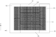
- FIG. 1 is a schematic diagram of a top view structure of a display panel provided by an embodiment of the disclosure
- FIG. 2 is a schematic cross-sectional view of a display panel provided by an embodiment of the disclosure.
- FIG. 3a is a schematic diagram of the top structure of the display panel
- Figure 3b is a schematic cross-sectional view at the dotted line L3 in Figure 3a;
- FIG. 3c is a schematic diagram of a display panel without a raised structure and a supporting structure after being tested
- 3d is a schematic diagram of a display panel provided with a raised structure and a supporting structure in an embodiment of the disclosure after inspection;
- FIG. 4 is a schematic cross-sectional view of another display panel provided by an embodiment of the disclosure.
- FIG. 5 is a schematic cross-sectional view of another display panel provided by an embodiment of the disclosure.
- FIG. 6 is a schematic cross-sectional view of another display panel provided by an embodiment of the disclosure.
- FIG. 7 is a schematic cross-sectional view of another display panel provided by an embodiment of the disclosure.
- FIG. 8 is a schematic diagram of a top view structure of another display panel provided by an embodiment of the disclosure.
- FIG. 9 is a schematic top view of another display panel provided by an embodiment of the disclosure.
- FIG. 10 is a schematic diagram of a top view structure of another display panel provided by an embodiment of the disclosure.
- FIG. 11 is a schematic diagram of a top view structure of another display panel provided by an embodiment of the disclosure.
- FIG. 12 is a schematic structural diagram of a display device provided by an embodiment of the disclosure.
- embodiments of the present disclosure provide a display panel and a display device.
- FIG. 1 is a schematic top view of the structure of a display panel provided by an embodiment of the present disclosure
- FIG. 2 is a cross-sectional view at the line L1 in FIG. 1.
- the display panel provided by the embodiment of the present disclosure, as shown in FIG. 1 and FIG. 2, includes:
- the cushion structure 101 is located on the first substrate 100 and in the non-display area B on at least one side of the display area A of the display panel;
- the supporting structure 102 is located on the side of the padding structure 101 away from the first substrate 100;
- the orthographic projection of the support structure 102 on the first substrate 100 is within the range of the orthographic projection of the cushion structure 101 on the first substrate 100.
- the raised structure can cushion the supporting structure, thereby improving the display panel’s position in the non-display area.
- the support ability of the area improves the resistance of the non-display area of the display panel to external impact, and improves the light leakage phenomenon that occurs at the edge of the display area.
- the orthographic projection of the supporting structure 102 on the first substrate 100 is within the range of the orthographic projection of the elevated structure 101 on the first substrate 100, so as to ensure that the elevated structure 101 can pad up the entire support structure 102.
- the support structure 102 To avoid the situation that a part of the support structure 102 is padded by the elevated structure 101 and the other part is not padded by the elevated structure 101, causing the support structure 102 to have a step on the side away from the first substrate 100, resulting in the support structure 102
- the support uniformity is poor, so as to ensure the support ability of the non-display area.
- the above-mentioned display panel is preferably a liquid crystal display panel, that is, the display panel may further include a liquid crystal layer
- the above-mentioned first substrate may be an array substrate, that is, the above-mentioned raised structure and the supporting structure may be located On the array substrate, or, the first substrate may also be a color filter substrate, that is, the raised structure and supporting structure may also be located on the color filter substrate.
- the positions of the raised structure and the supporting structure are not limited here.
- a raised structure and a supporting structure may be provided in the non-display area on at least one side of the display area. For example, if the display area is only one If light leakage occurs at the edge of the side, the raised structure and support structure can be provided only in the non-display area of the side.
- a raised structure and a support structure are provided in the non-display area on each side of the display area A .
- FIG. 3a is a schematic top view of the structure of the display panel
- FIG. 3b is a schematic cross-sectional view at the dotted line L3 in FIG. 3a.
- the display panel 302 can be placed on the machine 301, and a spacer 303 can be arranged between the display panel 302 and the machine 301, and the spacer 303 can be located
- the edge of the display panel 302 is used to detect the light leakage of the display panel 302 after being stressed by the gasket 303.
- Figure 3a in order to more clearly illustrate the top structure of the gasket 303, the figure will be blocked by the display panel 302 Part of the gasket 303 is indicated by a dotted line.
- the spacer 303 is used to apply stress to the display panel 302.
- other detection methods can also be used.
- a bead can be placed on the edge of the display panel 302 surface to apply stress to the non-display area.
- the detection method of the applied stress is not limited here, and it can be selected according to the actual situation.
- Figures 3c and 3d are schematic diagrams of physical objects after testing according to the above method.
- Figure 3c is a schematic diagram of a display panel without a raised structure and support structure after testing, that is, Figure 3c is a non-display area with poor supporting ability
- FIG. 3d is a schematic diagram of the display panel with a raised structure and a supporting structure in an embodiment of the disclosure after inspection.
- the display panel provided by the embodiment of the present disclosure has weak light leakage near the gasket 303. Also, take the light leakage area on the right side of the gasket 303 on the right as an example, and the figure is roughly marked by highlighting The light leakage area has a width d2 of approximately 3.1 mm and a height h2 of approximately 1.0 mm.
- the display panel provided by the embodiments of the present disclosure can significantly improve the light leakage phenomenon at the edge of the display panel.
- the display panel further includes: a color filter layer 103 located in the display area A;
- the color filter layer 103 includes at least three colors of sub-pixel color resistance (for example, in the figure, R represents the red sub-pixel color resistance, G represents the green sub-pixel color resistance, and B represents the blue sub-pixel color resistance), thereby Can make the display panel realize color light emission;
- the heightening structure 101 includes a color resistance structure of the same layer and the same material as the sub-pixel color resistance of at least one color.
- the color resist structure and the sub-pixel color resist in the cushion structure 101 are made of the same layer and the same material. In the manufacturing process, the color resist structure and the sub-pixel color resist can be manufactured by the same process, thereby reducing the manufacturing process and reducing the manufacturing cost.
- the display panel includes: a plurality of spacers located in the display area A; the spacers are located on the color filter layer 103 away from the first One side of the substrate 100;
- the plurality of spacers are divided into a plurality of main spacers 106a and a plurality of auxiliary spacers 106b;
- the sum of the height of the support structure 102 and the thickness of the cushion structure 101 is greater than the sum of the height of the main spacer 106 a and the thickness of the color filter layer 103.
- the thickness of all the film layers on the first substrate 100 in the non-display area B is greater than that of the first substrate 100. All the film layers on a substrate 100 are located at the thickness of the display area A, so that after the first substrate 100 and the second substrate are combined, the supporting structure 102 will be compressed so that the supporting structure 102 is supported on the first substrate 100 Between the second substrate 200 and the second substrate 200, the supporting ability of the display panel in the non-display area is ensured.
- the height of the support structure 102 and the thickness of the cushion structure 101 can be set It is sufficient to be slightly larger than the sum of the height of the main spacer 106a and the thickness of the color filter layer 103.
- the above-mentioned display panel provided by the embodiments of the present disclosure further includes: a second substrate 200 disposed opposite to the first substrate 100;
- the display panel further includes: a plurality of pixel units P arranged in an array in the display area A, and a plurality of pixel units P located on the side of the second substrate 200 facing the first substrate 100 extending in the first direction Y and Data lines arranged along the second direction X (not shown in the figure);
- the non-display area B is divided into two first sub-regions B1 located on both sides of the display area A along the first direction Y, and two second sub-regions B2 located on both sides of the display area A along the second direction X;
- the two directions X and the first direction Y are perpendicular to each other;
- the first sub-region B1 and the second sub-region B2 respectively include a cushion structure.
- strip spacers may be provided in the two first sub-regions B1 and the two second sub-regions B2 in FIG. ⁇ 102a.
- the raised structure includes at least two color resist structures.
- the raised structure may include a color resist structure 101a,
- the padding structure may include a color resistance structure 101a and a color resistance structure 101b;
- the orthographic projections of the color resist structures belonging to the same height structure on the first substrate have overlapping areas.
- the orthographic projections of the color resist structures 101a, 101b, and 101c on the first substrate 100 have overlapping areas. That is to say, the color resist structures 101a, 101b, and 101c are arranged in a layered manner.
- the orthographic projection of the color resist structures 101a and 101b on the first substrate has an overlapping area, that is, the color resist structures 101a and 101b Layered arrangement, so that different numbers of color resist structures can be superimposed to obtain height structures of different thicknesses.
- the number of color resist structures in the height structure can be determined according to actual needs, or half The tone mask is used to adjust the height of the color resist structure.
- different masks can be used to make sub-pixel color resists of different colors, and the color resist structure patterns can be set at the positions of at least two masks corresponding to the non-display area, so that The color resistance structure and the sub-pixel color resistance of the display area are made by the same patterning process.
- the color resist structure 101a and the red sub-pixel color resist in the display area A can be fabricated using the same patterning process, and the color resist structure 101b can be made using the same patterning process as the blue sub-pixel color resist in the display area A.
- the color resist structure 101c can be manufactured using the same patterning process as the green sub-pixel color resist in the display area A. Therefore, after three sub-pixel color resist patterning processes, a stacked three-layer color resist structure can be obtained (101a, 101b, and 101c).
- the color resist structures (101a, 101b, and 101c in the figure) belonging to the same heightened structure are formed on the first substrate 100.
- the orthographic projections do not overlap.
- the same mask can be used to make sub-pixel color resists of different colors.
- the mask is provided with sub-pixel patterns at positions corresponding to the display area.
- the pattern of the color resist structure is provided at the position corresponding to the non-display area.
- the mask can be used to first make the red sub-pixel color resist, thereby forming the red color resist structure 101c in the non-display area. Then, the mask is shifted by one pixel unit distance, and then a blue sub-pixel color resist is fabricated. At the same time, a blue color resist structure 101b is formed in the non-display area. Finally, the mask is shifted by a pixel unit distance, and then fabricated The green sub-pixel color resistance will also form a green color resistance structure 101a in the non-display area.
- the distance of more pixel units can also be staggered when making sub-pixel color resists of different colors, and the total staggered distance is an integer multiple of the size of the pixel unit.
- the color order of making sub-pixel color resists can also be determined according to actual needs, which is not limited here.
- the orthographic projections of the color resist structures belonging to the same raised structure on the first substrate 100 do not overlap.
- the color resist structure can use the same patterning process as the sub-pixel color resist in the display area, and use the same mask to make color resist structures of different colors, thereby saving the number of masks and reducing the process production cost.
- the embodiment of the present disclosure preferably adopts the structure shown in FIG. 7 or FIG. 6.
- the pad height structure 101 includes three-color color resist structures; in the second sub-region B2, the pad The high structure 101 includes a color resistance structure of one color.
- the second sub-region B2 on the left in the figure includes a plurality of red color resistance structures, and the second sub-region B2 on the right in the figure includes a plurality of green colors.
- the color resist structures are arranged in a row in the second direction X, and the color resist structures of three colors are alternately arranged;
- the color resist structures are arranged in a row in the first direction Y.
- the pixel units P in the general display area A are arranged in an array, and the width of each color resist structure in the first sub-region B1 in the second direction X can be set to be the same as the pixel unit P in the second direction.
- the width in the direction X is the same, and the width of each color resist structure in the second sub-region B2 in the first direction Y is set to be the same as the width of the pixel unit P in the first direction Y, which is convenient for viewing the non-display area Layout of the heightened structure.
- the height-up structure in the second sub-region can also be an integrated structure, that is, the height-up structure is composed of a color resistance structure.
- the height-up structure is composed of a color resistance structure.
- a color resistance structure For example, only one red color can be provided in the second sub-region on the left.
- the color resistance structure only one green color resistance structure can be provided in the second sub-region on the right, and color resistance structures of other colors can also be provided in the second sub-region, which is not limited here.
- the color resistance structure is connected with the first sub-pixel color resistance to form an integrated structure
- the first sub-pixel color resistance is the sub-pixel color resistance at the edge of the display area A, the first sub-pixel color resistance is adjacent to the color resistance structure, and the colors of the first sub-pixel color resistance and the color resistance structure are the same.
- the three-color pixel units P in each row are alternately arranged.
- the pixel units P in each row have the same color.
- the color resistance structure in the display area is set to be an integrated structure with the first sub-pixel color resistance. As long as each pixel unit at the edge of the display area is extended to the non-display area, it is more beneficial to the color resistance structure in the non-display area. Composition.
- three different masks can be used to make sub-pixel color resists of different colors, and in the mask for making red sub-pixel color resists, corresponding to two
- the first sub-area B1 and the second sub-area B2 on the left are provided with patterns of the raised structure.
- the patterns of the raised structure can be set in the mask for making blue and green sub-pixel color resists. Therefore, while fabricating the sub-pixel color resistance in the display area, the height structure in the non-display area is fabricated.
- the height-up structure 101 includes three-color color resist structures; in the second sub-region B2 , the padding structure 101 includes three-color color resistance structure;
- the color resist structures are arranged in a row in the second direction X, and the color resist structures of three colors are alternately arranged;
- the color resist structures are arranged in a row in the second direction X, and the color resist structures of three colors are alternately arranged.
- the color resist structures are alternately arranged in the second direction X. Therefore, in the actual process, the same mask can be used to produce different colors Color resistance structure.
- the raised structure in the non-display area may also be configured to consist of only one color resist structure, that is, the raised structure may be an integral structure.
- the raised structure may be distributed at the position where the display area extends to the non-display area, as shown in FIG. 8, or the raised structure may also be distributed at other positions except the display area extends to the non-display area, as shown in FIG.
- the specific distribution of the raised structure in the non-display area is not limited here, and the specific distribution of the raised structure can be set according to actual needs.
- the above-mentioned display panel provided by an embodiment of the present disclosure further includes: a light shielding layer 104 located between the raised structure 101 and the first substrate 100, and a light shielding layer 104 located between the raised structure 101 and the first substrate 100; 100 side flat layer 105.
- the light-shielding layer 104 extends into the non-display area B, which can prevent light leakage in the non-display area and ensure the display effect of the display panel, and the light-shielding layer 104 located in the non-display area B can further heighten the support structure 102. Further improve the support ability of the display panel in the non-display area.
- Extending the planarization layer 105 into the non-display area B can planarize the film layers in the non-display area B, and the orthographic projection of the planarization layer 105 on the first substrate 100 and the cushion structure 101 on the first substrate 100
- the above orthographic projection has an overlapping area. Therefore, the part of the flat layer 105 extending into the non-display area B can further elevate the support structure 102 and further improve the support ability of the display panel at the non-display area.
- the above-mentioned heightening structure is composed of a color resist structure of the same layer and the same material as the sub-pixel color resist of at least one color, which is an implementation manner in the embodiment of the present disclosure.
- the above-mentioned raised structure can also be the same layer and the same material as other film layers, for example, it can be the same layer and the same material as the flat layer or the light-shielding layer, or the patterning process can also be used to make the raised structure separately in the non-display area. limited.
- the end surface of the support structure 102 facing away from the first substrate 100 is in contact with the surface of the second substrate 200 facing the first substrate 100, so that The support ability of the display panel in the non-display area is further improved, the ability of the display panel to resist external impact in the non-display area is further improved, and the light leakage phenomenon that occurs at the edge of the display area is improved.
- the height of the support structure 102 can be combined to determine the thickness of the cushion structure 101 to ensure that the end surface of the support structure 102 on the side facing away from the first substrate 100 and the surface of the second substrate 100 facing the first substrate 100 contact.
- the non-display area B further includes: a metal layer 201 on the side of the second substrate 200 facing the first substrate 100;
- each supporting structure 102 on the second substrate 200 is within the range of the orthographic projection of the metal layer 201 on the second substrate 200.
- the support structures 102 in the non-display area B are all occupied on the metal layer 201, so that the compression amount of the support structures 102 can be ensured to be consistent, so that the support capacity in the non-display area B is uniform.
- the above-mentioned metal layer may be a film layer such as a gate layer or a source/drain metal layer.
- the metal layer is not limited here, as long as each supporting structure 102 is supported on the same metal layer. It should be noted that the support structure 102 and the metal layer 201 are not in direct contact, and an insulating layer 203 can also be provided between the metal layer 201 and the support structure 102.
- the support structures 102 in the non-display area B may all occupy areas outside the pattern of the metal layer 201, and the support capacity of the non-display area B can also be made uniform.
- the non-display area B further includes: a sealant 202 located between the first substrate 100 and the second substrate 200;
- the frame sealant 202 is located at the edge of the display panel
- the height-up structure 101 is located between the frame sealant 202 and the display area A, and there is a gap C between the height-up structure 101 and the frame sealant 202.
- the first substrate 100 and the second substrate 200 are fixed by the frame sealant 202.
- the frame sealant 202 In order to ensure that the heightened structure 101 does not affect the diffusion of the frame sealant 202 and ensure the packaging effect of the display panel, it is necessary to ensure that the heightened structure 101 and the frame sealant There is a certain distance C between 202.
- the distance C between the heightening structure 101 and the frame sealant 202 is greater than the position accuracy of the frame sealant 202 and the spread of the frame sealant 202 The sum of the accuracy and the position accuracy of the raised structure 101.
- the distance C between the above-mentioned cushion structure 101 and the frame sealant 202 needs to be greater than the position accuracy of the frame sealant 202 and the spread of the frame sealant 202 The sum of the accuracy and the position accuracy of the raised structure 101.
- the above-mentioned spacing C is equal to the difference between the distance between the sealant 202 and the edge of the display area A and the size of N pixel units, where N is an integer,
- the spacing C needs to be greater than the sum of the position accuracy of the frame sealing compound 202, the spreading accuracy of the encapsulation compound 202, and the position accuracy of the cushion structure 101.
- the position accuracy of the frame sealing glue can be understood as the difference between the design position and the actual position of the frame sealing glue.
- the glue-like encapsulant is first applied to the edge of the first substrate (or the second substrate), and the frame sealant is cured after the first substrate and the second substrate are in the box.
- the sealing glue because the sealing glue has fluidity, it will spread in a certain area.
- the spreading accuracy of the frame sealing glue can be understood as the size of the area where the sealing glue can spread.
- the position accuracy of the elevated structure can be understood as the difference between the design position and the actual position of the elevated structure.
- the distance D between the support structure 102 farthest from the display area A on the side away from the display area A and the edge of the raised structure 101 on the side away from the display area A is D, and refer to FIG. 7 Considering that the raised structure 101 may be composed of multiple color resist structures that are staggered with each other, the distance D needs to be greater than the size of the pixel unit to ensure that the support structure 102 can occupy the flat raised structure 101 to ensure support Uniformity of ability.
- the sealant 202 needs to be cured by light.
- a light-shielding layer 104 is provided on the side of the first substrate 100 Therefore, the metal layer 201 and the insulating layer 203 on the second substrate 200 can be patterned to form a plurality of through holes at positions corresponding to the sealant 202, so that the process can be performed on one side of the second substrate 200.
- Light is applied to cure the frame sealant 202.
- the distance between adjacent support structures 102 is E, which can be combined with the position of the support structure 102 in the display panel.
- the pattern distribution of the metal layer 201 can be considered to determine the size of the distance E
- the distance E can be between 100 ⁇ m and 1000 ⁇ m, and the distance E can also be set according to actual conditions, which is not limited here.
- the display area A further includes: a plurality of spacers on the side of the color filter layer 103 away from the first substrate 100 (as shown in FIG. Septa 106a and 106b);
- the support structure 102 and the spacer are of the same layer and material.
- the support structure 102 and the spacer can be manufactured using the same patterning process, thereby saving process steps and reducing manufacturing costs.
- the spacer that can contact both the surfaces of the first substrate 100 and the second substrate 200 is the main spacer 106a, and only the surface of the first substrate 100 is in contact with the surface of the second substrate 200.
- the spacer that is not in contact with the surface is the auxiliary spacer 106b. Since the support structure 102 has a height-up structure 101, the height of the support structure 102 can be set to be the same as the height of the auxiliary spacer 106b. The thickness of the supporting structure 102 is supported between the first substrate 100 and the second substrate 200.
- the support structure 102 and the auxiliary spacer 106b can be made by the same patterning process, or the support structure 102, the main spacer 106a and the auxiliary spacer 106b can also be made of halftone masks to achieve Made by the same composition process.
- the above-mentioned supporting structure includes: strip spacers 102a, and at least one strip spacer 102a extends in the first direction Y or extends in the second direction X.
- the strip spacer 102a When space permits, the strip spacer 102a extending in the first direction Y or the second direction X is used.
- the strip spacer 102a can support a larger range, which can make the non-display area B have a better support effect. Great.
- the position of M in the display area A indicates the position of the main spacer
- the position of S indicates the position of the auxiliary spacer.
- the main spacer can be determined according to the actual situation.
- the distribution of the spacer M and the auxiliary spacer S is not limited to the distribution of the main spacer M and the auxiliary spacer S.
- at least two rows of strip spacers can be provided, and the number of strip spacers can be determined according to the required contact density.
- the gap between the plurality of pixel units P in the second direction X is the first gap
- each strip spacer 102a extends along the second direction X, and each strip spacer 102a is arranged in an array, and at least part of the strip spacer 102a is perpendicular to the second direction X
- the orthographic projection on the plane of the direction has an overlap area with the orthographic projection of the first gap on the plane perpendicular to the second direction X.
- Each dotted line L2 in FIG. 1 represents a straight line where the first gap is located.
- the alignment layer on the surface of the first substrate needs to be rubbed orientated.
- a roller can be used for rolling friction along the second direction X, in order to avoid strip spacers.
- the strip spacer 102a can be arranged at the position where the first gap extends to the non-display area.
- each strip spacer 102a in the second sub-region B2 is located at the position of the dotted line L2.
- the roller corresponds to each first A gap position is in contact with the strip spacer 102a, so as to ensure that the roller does not contact the strip spacer 102a at the position corresponding to each pixel unit, so as to ensure that the roller is not damaged at the position corresponding to each pixel unit , To ensure that the display panel has a better display effect.
- the length of each strip spacer 102a in the second direction X is less than or equal to two values as much as possible.
- the structure shown in FIG. 1 has a length in the first direction Y.
- the length of one row of strip spacers 102a can take the first value
- the length of the other row of strip spacers 102a can take the second value
- the specific value of the length of strip spacers 102a can take the pixel unit size.
- the distance between the strip spacers 102a closest to the display area A and the display area A is greater than or equal to 0.5 mm.
- all the strip spacers 102a are located where the first gap extends to the non-display area, so that the influence of the strip spacers 102a on the rubbing orientation process is minimized.
- each strip spacer 102a extends along the first direction Y;
- the orthographic projections of the strip spacers 102a located in the same second sub-region B2 on a plane perpendicular to the second direction X form a continuous pattern.
- each strip spacer 102a on a plane perpendicular to the second direction X constitutes a continuous pattern.
- the roller rolls along the second direction X The influence of each strip spacer 102a on the roller is relatively uniform, thereby reducing the influence of the strip spacer 102a on the roller and ensuring the display effect of the display panel.
- the distance between the strip spacer closest to the display area and the display area is greater than or equal to 1.5 mm.
- the farther the distance from the display region A the longer the length of the strip spacer 102a in the first direction. Long, which can effectively block foreign objects and prevent foreign objects from entering the display area A.
- the distance between the strip spacer closest to the display area and the display area is greater than or equal to 1.5 mm.
- each strip-shaped spacer 102a extends along the second direction X;
- the orthographic projections of the strip spacers 102a located in the same first sub-region B1 on a plane perpendicular to the first direction Y form a continuous pattern.
- each stripe spacer 102a extends along the second direction X, which can effectively block foreign objects and prevent foreign objects from entering the display area A, and will belong to the same first sub-region B1.
- the strip spacers 102a are arranged in a staggered arrangement so that the orthographic projection of the strip spacers 102a on a plane perpendicular to the first direction Y forms a continuous pattern, which can further enhance the ability to block foreign objects.
- at least two rows of strip spacers can be provided, and the number of strip spacers can be determined according to the required contact density.
- the length of each strip spacer 102a in the second direction X is less than or equal to two values as far as possible.
- the length of each strip spacer 102a can be the same, or can be set Take the first value for the length of each strip spacer in the first row and the third row, and take the second value for the length of each strip spacer in the second row.
- the length of the strip spacer can be Take an integer multiple of the pixel unit size.
- the specific space in the first sub-region B1 and the second sub-region B2 can be combined to determine the size of the strip spacer 102a at different positions, that is, the strip spacer 102a can be adjusted according to the actual situation.
- the length of 102a in the first direction Y or the length of the second direction X, for example, the width of the strip spacer 102a may be set in the range of 20 ⁇ m to 80 ⁇ m.
- the distance between the strip spacer closest to the display area and the display area is greater than or equal to 1.5 mm.
- the contact density of the support structure in the first sub-region B1 may be greater than 10000 ⁇ m 2 /mm 2 ;
- the contact density of the support structure of B2 in the second subregion is greater than 5000 ⁇ m 2 /mm 2 .
- the contact density requirements of the first sub-region B1 and the second sub-region B2 can be combined with the pattern distribution of other related film layers in the display panel.
- the supporting structure is arranged in a medium manner to ensure that the display panel has a good supporting ability in both the first sub-region B1 and the second sub-region B2.
- each support structure in the non-display area is uniform.
- the extending direction of each strip support structure 102a is the same.
- the compression amount of the above-mentioned support structure is in the range of 0.1-0.3 ⁇ m.
- the height of the support structure 102 manufactured on the first substrate 100 is slightly higher than the distance between the flat layer 105 and the metal layer 201, which is greater than
- the difference in the height of the supporting structure 102 is the amount of compression. Therefore, after the first substrate 100 and the second substrate 200 are assembled, the supporting structure 102 is compressed so that the supporting structure 102 is supported between the first substrate 100 and the second substrate 200. During the period, the support ability of the display panel in the non-display area is guaranteed. In addition, the amount of compression is too large, resulting in poor yellow light at this position. Therefore, the amount of compression can be set in the range of 0.1 to 0.3 ⁇ m, that is, the height of the support structure 102 is slightly higher than that between the flat layer 105 and the metal layer 201. Distance is enough.
- the supporting structure may further include: dot spacers 102b;
- the dotted spacers 102b are distributed in the gaps of the striped spacers 102a.
- dot spacers 102b can also be arranged at the gaps of the strip spacers 102a.
- the plane size of the dot spacers 102b is smaller than the plane size of the strip spacers 102a. Therefore, the dot spacer 102b can be arranged in a position with a small space.
- strip spacers 102a with a regular arrangement can be preferentially used.
- the dotted spacer 102b is represented by a circle, and the shape of the dotted spacer 102b is not limited. In specific implementation, the shape of the dotted spacer 102b can be a circle, a square, a triangle, etc. .
- the embodiments of the present disclosure also provide a display device, which can be applied to any product or component with display function such as mobile phones, tablet computers, televisions, monitors, notebook computers, digital photo frames, navigators, etc. . Since the principle of solving the problems of the display device is similar to that of the above-mentioned display panel, the implementation of the display device can refer to the implementation of the above-mentioned display panel, and the repetition will not be repeated.
- the above-mentioned display device provided by an embodiment of the present disclosure, referring to FIG. 12, includes: the above-mentioned display panel, and a backlight module located on the light-incident side of the display panel;
- the backlight module includes a backlight source located on one side of the display device, that is, the backlight module is an edge-type backlight module.
- the backlight source 304 located in the first sub-region B1 includes a plurality of light sources 305.
- the light source 305 may be a light emitting diode (LED) light source; in addition, in the backlight module
- it can also include a light guide plate.
- the backlight in the backlight module can be arranged on one side of the light guide plate. The light of the backlight can be emitted as a surface light source through the light guide plate, thereby realizing the function of providing a light source for the display panel. .
- the heightening structure can have at least the following two setting modes:
- the heightening structure corresponding to the side of the backlight includes at least two stacked color resist structures. Since the color resist structure and the color filter layer of the display area are of the same layer and material, the color resist structure also has The light filtering function enables the color resist structure to reduce the light intensity of the light passing through the color resist structure, and superimposing the color resist structure can further reduce the light intensity of the light passing through the raised structure, or completely absorb the light directed to the raised structure Light to alleviate light leakage.
- the pad height structure shown in FIG. 5 includes a laminated color resist structure 101a, a color resist structure 101b, and a color resist structure 101c. Since the color resist structures 101a, 101b, and 101c are connected with the red sub-pixel color resist and the blue sub-pixel color resist, respectively , The green sub-pixel color resistance is the same layer and the same material. After the light directed to the raised structure passes through the color resistance structure 101c, only the green light can be emitted, the red and blue light will be absorbed by the color resistance structure 101a, and the green light passes through After passing through the color resist structure 101c, it is directed toward the color resist structure 101b. Since only blue light can pass through the color resist structure 101b, the light cannot pass through the color resist structure 10b, so that the raised structure plays a role of shading.
- the principle of shading by the raised structure in the display panel shown in FIG. 6 is similar to that in FIG.
- the height structure corresponding to the side of the backlight source includes a color resistance structure. Similar to the light-shielding principle in Mode 1, when only one color resist structure is included in the heightened structure, since the color resist structure has a filtering effect, the color resist structure can reduce the intensity of light passing through the color resist structure.
- the color resist structure in the cushion structure can be set to the same layer and the same material as the red or blue sub-pixel color resist, so the color resist structure can filter out the green color. Light, thereby alleviating light leakage.
- the raised structure can padded the support structure, thereby improving the display panel
- the support capacity of the non-display area improves the resistance of the non-display area of the display panel to external impact, and improves the light leakage phenomenon that occurs at the edge of the display area.
- the color resist structure and the color filter layer of the display area are of the same layer and material, the color resist structure also has a filtering effect, so that the color resist structure can reduce the light intensity of the light passing through the color resist structure. After being superimposed, the light intensity of the light passing through the elevated structure can be further reduced, or the light directed to the elevated structure can be completely absorbed to alleviate the light leakage phenomenon.
Landscapes
- Physics & Mathematics (AREA)
- Nonlinear Science (AREA)
- Mathematical Physics (AREA)
- Chemical & Material Sciences (AREA)
- Crystallography & Structural Chemistry (AREA)
- General Physics & Mathematics (AREA)
- Optics & Photonics (AREA)
- Devices For Indicating Variable Information By Combining Individual Elements (AREA)
- Liquid Crystal (AREA)
Abstract
本公开实施例提供了一种显示面板及显示装置,该显示面板,包括:第一基板;垫高结构,位于第一基板之上,且位于显示面板的显示区域至少一侧的非显示区域内;支撑结构,位于垫高结构背离第一基板的一侧;其中,支撑结构在第一基板上的正投影位于垫高结构在第一基板上的正投影的范围内。
Description
本公开涉及显示技术领域,尤其一种显示面板及显示装置。
液晶显示器(Liquid Crystal Display,LCD)经过最近几十年的发展,技术和工艺日趋成熟,已经取代冷阴二极管(Cold Cathode Fluorescent Lamp,CCFL)显示器,成为显示领域的主流产品。
在对液晶显示器进行整机模组制作过程中,需要在周边的非显示区域加装边框,或者在非显示区域下方粘贴泡棉双面胶,从而使液晶显示面板固定于整机的背板边框上。
然而,边框或泡棉双面胶会产生一定的应力作用于非显示区域,由于液晶显示器的非显示区域处的支撑能力较差,当应力作用于周边的非显示区域时,会产生较大的形变,并且该形变会向显示区域传导,一方面会使显示区域边缘处的玻璃基板产生相位延迟,导致出射光的偏振状态改变,另一方面也会使显示区域边缘处的液晶盒厚发生变化,导致液晶排布混乱,从而导致显示区域的边缘处出现漏光现象。
发明内容
本公开实施例提供的一种显示面板,其中,包括:
第一基板;
垫高结构,位于所述第一基板之上,且位于所述显示面板的显示区域至少一侧的非显示区域内;
支撑结构,位于所述垫高结构背离所述第一基板的一侧;
其中,所述支撑结构在所述第一基板上的正投影位于所述垫高结构在所述第一基板上的正投影的范围内。
可选地,在本公开实施例中,所述显示面板还包括:位于所述显示区域内的彩色滤光层,以及位于所述彩色滤光层背离所述第一基板一侧的多个隔垫物;
所述彩色滤光层包括至少三种颜色的亚像素色阻;
所述垫高结构包括:与至少一种颜色的所述亚像素色阻同层同材质的色阻结构;
所述支撑结构与所述隔垫物同层同材质;
所述显示面板还包括:位于所述垫高结构与所述第一基板之间的遮光层,以及位于所述垫高结构背离所述第一基板一侧的平坦层。
可选地,在本公开实施例中,多个所述隔垫物分为多个主隔垫物和多个副隔垫物;
所述支撑结构的高度与所述垫高结构的厚度之和,大于所述主隔垫物的高度与所述彩色滤光层的厚度之和。
可选地,在本公开实施例中,还包括:与所述第一基板相对设置的第二基板;
所述显示面板还包括:位于所述显示区域内呈阵列排布的多个像素单元,以及位于所述第二基板面向所述第一基板一侧的多条沿第一方向延伸且沿第二方向排布的数据线;
所述非显示区域分为位于所述显示区域沿所述第一方向上两侧的两个第一子区域,以及位于所述显示区域沿第二方向上两侧的两个第二子区域;所述第二方向与所述第一方向相互垂直;
所述第一子区域和所述第二子区域分别包括一个所述垫高结构。
可选地,在本公开实施例中,所述垫高结构包括至少两个色阻结构;
属于同一个所述垫高结构中的各所述色阻结构在所述第一基板上的正投影具有交叠区域。
可选地,在本公开实施例中,属于同一个所述垫高结构的各所述色阻结构在所述第一基板上的正投影不交叠。
可选地,在本公开实施例中,在所述第一子区域中,所述垫高结构包括三种颜色的所述色阻结构;在所述第二子区域中,所述垫高结构包括一种颜色的所述色阻结构;
位于所述第一子区域的所述垫高结构中,各所述色阻结构在所述第二方向上排列成一排,且三种颜色的所述色阻结构交替排列。
可选地,在本公开实施例中,所述色阻结构与第一亚像素色阻相连构成一体结构;
所述第一亚像素色阻为所述显示区域边缘的亚像素色阻,所述第一亚像素色阻与所述色阻结构相邻,且所述第一亚像素色阻与所述色阻结构的颜色相同。
可选地,在本公开实施例中,在所述第一子区域中,所述垫高结构包括三种颜色的所述色阻结构;在所述第二子区域中,所述垫高结构包括三种颜色的所述色阻结构;
位于所述第一子区域的所述垫高结构中,各所述色阻结构在所述第二方向上排列成一排,且三种颜色的所述色阻结构交替排列;
位于所述第二子区域的所述垫高结构中,各所述色阻结构在所述第二方向上排列成一排,且三种颜色的所述色阻结构交替排列。
可选地,在本公开实施例中,所述支撑结构背离所述第一基板一侧的端面与所述第二基板面向所述第一基板一侧的表面接触。
可选地,在本公开实施例中,在所述非显示区域内还包括:位于所述第二基板面向所述第一基板一侧的金属层;
各所述支撑结构在所述第二基板上的正投影位于所述金属层在所述第二基板上的正投影的范围内。
可选地,在本公开实施例中,在所述非显示区域内还包括:位于所述第一基板与所述第二基板之间的封框胶;
所述封框胶位于所述显示面板的边缘;
所述垫高结构位于所述封框胶与所述显示区域之间,且所述垫高结构与 所述封框胶之间存在间距;
所述垫高结构与所述封框胶之间的间距大于所述封框胶的位置精度、所述封框胶的扩散精度以及所述垫高结构的位置精度的总和。
可选地,在本公开实施例中,所述支撑结构包括:条状隔垫物,至少一个所述条状隔垫物沿所述第一方向延伸或沿所述第二方向延伸。
可选地,在本公开实施例中,多个所述像素单元在所述第二方向上的间隙为第一间隙;
在所述第二子区域内,各所述条状隔垫物沿所述第二方向延伸,且各所述条状隔垫物呈阵列排布,至少部分所述条状隔垫物在垂直于所述第二方向的平面上的正投影,与所述第一间隙在垂直于所述第二方向的平面上的正投影具有重叠区域。
可选地,在本公开实施例中,在所述第二子区域内,距离所述显示区域最近的所述条状隔垫物与所述显示区域之间的间距大于或等于0.5mm。
可选地,在本公开实施例中,在所述第二子区域内,各所述条状隔垫物沿所述第一方向延伸;
位于同一个所述第二子区域内的各所述条状隔垫物,在垂直于所述第二方向的平面上的正投影构成连续图形;
在所述第二子区域内,与所述显示区域的距离越远,所述条状隔垫物在所述第一方向上的长度越长。
可选地,在本公开实施例中,在所述第二子区域内,距离所述显示区域最近的所述条状隔垫物与所述显示区域之间的间距大于或等于1.5mm。
可选地,在本公开实施例中,在所述第一子区域内,各所述条状隔垫物沿所述第二方向延伸;
位于同一个所述第一子区域中的各所述条状隔垫物,在垂直于所述第一方向的平面上的正投影构成连续图形;
在所述第一子区域内,与所述显示区域的距离越远,所述条状隔垫物在所述第二方向上的长度越长。
可选地,在本公开实施例中,在所述第一子区域内,距离所述显示区域最近的所述条状隔垫物与所述显示区域之间的间距大于或等于1.5mm。
可选地,在本公开实施例中,所述第一子区域内的所述支撑结构的接触密度大于10000μm
2/mm
2;
所述第二子区域内的所述支撑结构的接触密度大于5000μm
2/mm
2;
所述支撑结构的压缩量在0.1~0.3μm的范围内。
可选地,在本公开实施例中,所述支撑结构还包括:点状隔垫物;
所述点状隔垫物分布于所述条状隔垫物的间隙处。
相应地,本公开实施例还提供了一种显示装置,包括:上述显示面板,以及位于所述显示面板入光面一侧的背光模组;
所述背光模组,包括位于所述显示装置一侧的背光源;
所述背光源所在侧对应的垫高结构包括至少两个层叠的色阻结构;
或,
所述背光源所在侧对应的所述垫高结构包括一个所述色阻结构。
图1为本公开实施例提供的一种显示面板的俯视结构示意图;
图2为本公开实施例提供的一种显示面板的截面示意图;
图3a为显示面板的俯视结构示意图;
图3b为图3a中虚线L3处的截面示意图;
图3c为不设置垫高结构和支撑结构的显示面板进行检测后的示意图;
图3d为本公开实施例中设置垫高结构和支撑结构的显示面板进行检测后的示意图;
图4为本公开实施例提供的另一种显示面板的截面示意图;
图5为本公开实施例提供的另一种显示面板的截面示意图;
图6为本公开实施例提供的另一种显示面板的截面示意图;
图7为本公开实施例提供的另一种显示面板的截面示意图;
图8为本公开实施例提供的另一种显示面板的俯视结构示意图;
图9为本公开实施例提供的另一种显示面板的俯视结构示意图;
图10为本公开实施例提供的另一种显示面板的俯视结构示意图;
图11为本公开实施例提供的另一种显示面板的俯视结构示意图;
图12为本公开实施例提供的一种显示装置的结构示意图。
针对液晶显示器的非显示区域处的支撑能力较差,容易导致显示区域的边缘处出现漏光现象的技术问题,本公开实施例提供了一种显示面板及显示装置。
下面结合附图,对本公开实施例提供的显示面板及显示装置的具体实施方式进行详细地说明。附图中各部分的大小和形状不反映真实比例,目的只是示意说明本公开内容。
图1为本公开实施例提供的显示面板的俯视结构示意图,图2为图1中直线L1处的截面图。
本公开实施例提供的显示面板,如图1和图2所示,包括:
第一基板100;
垫高结构101,位于第一基板100之上,且位于显示面板的显示区域A至少一侧的非显示区域B内;
支撑结构102,位于垫高结构101背离第一基板100的一侧;
其中,支撑结构102在第一基板上100的正投影位于垫高结构101在第一基板100上的正投影的范围内。
本公开实施例提供的上述显示面板中,通过在显示区域至少一侧的非显示区域内设置垫高结构和支撑结构,垫高结构可以将支撑结构垫起,从而提高了显示面板在该非显示区域的支撑能力,提高了显示面板的非显示区域抗外力冲击能力,改善显示区域的边缘处出现的漏光现象。
如图2所示,支撑结构102在第一基板100上的正投影位于垫高结构101 在第一基板100上的正投影的范围内,从而保证垫高结构101能够将整个支撑结构102垫起,避免出现支撑结构102的一部分被垫高结构101垫起,另一部分没有被垫高结构101垫起的情况,使支撑结构102在背离第一基板100的一侧产生段差,导致支撑结构102的支撑均一性较差,从而保证非显示区域的支撑能力。
具体地,本公开实施例中,上述显示面板优选为液晶显示面板,也就是说,该显示面板还可以包括液晶层,上述第一基板可以为阵列基板,即上述垫高结构和支撑结构可以位于阵列基板上,或者,上述第一基板也可以为彩膜基板,即上述垫高结构和支撑结构也可以位于彩膜基板上,此处不对垫高结构和支撑结构的位置进行限定。
在具体实施时,本公开实施例中,可以根据显示面板的显示区域的漏光情况,在显示区域的至少一侧的非显示区域内设置垫高结构和支撑结构,例如,如果显示区域仅在一侧的边缘处出现漏光现象,则可以仅在该侧的非显示区域内设置垫高结构和支撑结构。
可选地,为了保证显示区域的每一侧的边缘处都不会出现漏光现象,如图1所示,在显示区域A的每一侧的非显示区域内均设有垫高结构和支撑结构。
图3a为显示面板的俯视结构示意图,图3b为图3a中虚线L3处的截面示意图。
在具体实施时,如图3a和图3b所示,可以通过将显示面板302放置于机台301之上,并在显示面板302与机台301之间设置垫片303,且将垫片303位于显示面板302的边缘处,来检测显示面板302受到垫片303带来的应力后的漏光情况,在图3a中,为了更清楚的示意垫片303的俯视结构,图中将被显示面板302遮挡的部分垫片303以虚线表示。
本公开实施例中采用垫片303来对显示面板302施加应力,在具体实施时,也可以采用其他检测方法,例如可以在显示面板302表面的边缘处放置压条,来向非显示区域施加应力,此处不对施加应力的检测方法进行限定, 可以根据实际情况进行选择。
图3c和图3d为按照上述方法进行检测后的实物示意图,其中,图3c为不设置垫高结构和支撑结构的显示面板进行检测后的示意图,即图3c为非显示区域支撑能力较差的显示面板的进行检测后的示意图,图3d为本公开实施例中设置垫高结构和支撑结构的显示面板进行检测后的示意图。
从图3c可以明显看出,非显示区域的支撑能力较差的显示面板,在垫片303的附近漏光现象比较严重,以右侧的垫片303右边的漏光区域为例,图中以弧线大致标出漏光区域的范围,该漏光区域的宽度d1约为5.5mm,高度h1约为2.3mm。
从图3d可以明显看出,本公开实施例提供的显示面板,在垫片303附近的漏光现象较弱,同样以右侧的垫片303右边的漏光区域为例,图中以凸显大致标出漏光区域的范围,该漏光区域的宽度d2约为3.1mm,高度h2约为1.0mm。
因此,通过对比图3c和图3d中漏光区域的大小,以及漏光区域处的漏光强度可以明显看出,本公开实施例提供的显示面板可以明显改善显示面板边缘处的漏光现象。
具体地,本公开实施例提供的上述显示面板中,如图2所示,显示面板还包括:位于显示区域A内的彩色滤光层103;
彩色滤光层103包括至少三种颜色的亚像素色阻(例如,图中R表示红色的亚像素色阻,G表示绿色的亚像素色阻,B表示蓝色的亚像素色阻),从而可以使显示面板实现彩色出光;
垫高结构101包括:与至少一种颜色的亚像素色阻同层同材质的色阻结构。
垫高结构101中的色阻结构与亚像素色阻同层同材质,在制作工艺过程中,色阻结构可以与亚像素色阻采用同一工艺制作,从而可以减少制作工艺,降低制作成本。
在具体实施时,本公开实施例提供的上述显示面板中,如图2所示,显 示面板,包括:位于显示区域A内的多个隔垫物;隔垫物位于彩色滤光层103背离第一基板100的一侧;
多个隔垫物分为多个主隔垫106a物和多个副隔垫物106b;
支撑结构102的高度与垫高结构101的厚度之和,大于主隔垫物106a的高度与彩色滤光层103的厚度之和。
如图2所示,也就是说,在第一基板100之上的其他膜层的厚度一致的情况下,第一基板100之上的所有膜层在位于非显示区域B的厚度,要大于第一基板100之上的所有膜层在位于显示区域A的厚度,从而在后续第一基板100与第二基板对盒后,支撑结构102会被压缩,以使支撑结构102支撑于第一基板100与第二基板200之间,保证显示面板在非显示区域的支撑能力。
在具体实施时,为了保证对盒后的显示面板在显示区域A和非显示区域B的盒后一致,防止出现显示不良现象,可将支撑结构102的高度与垫高结构101的厚度之和设置为,稍大于主隔垫物106a的高度与彩色滤光层103的厚度之和即可。
在实际应用中,本公开实施例提供的上述显示面板中,如图4所示,还包括:与第一基板100相对设置的第二基板200;
如图1所示,显示面板还包括:位于显示区域A内呈阵列排布的多个像素单元P,以及位于第二基板200面向第一基板100一侧的多条沿第一方向Y延伸且沿第二方向X排布的数据线(图中未示出);
非显示区域B分为位于显示区域A沿第一方向Y上两侧的两个第一子区域B1,以及位于显示区域A沿第二方向上X两侧的两个第二子区域B2;第二方向X与第一方向Y相互垂直;
第一子区域B1和第二子区域B2分别包括一个垫高结构。
具体地,为了保证显示区域的每一侧的边缘处都不会出现漏光现象,可以在图1中的两个第一子区域B1和两个第二子区域B2中均设置有条状隔垫物102a。
具体地,本公开实施例提供的上述显示面板中,如图5和图6所示,垫高结构包括至少两个色阻结构,如图5所示,垫高结构可以包括色阻结构101a、色阻结构101b和色阻结构101c,如图6所示,垫高结构可以包括色阻结构101a和色阻结构101b;
属于同一个垫高结构中的各色阻结构在第一基板上的正投影具有交叠区域,如图5中,色阻结构101a、101b和101c在第一基板100上的正投影具有交叠区域,也就是说,色阻结构101a、101b和101c层叠设置,如图6中,色阻结构101a和101b在第一基板上的正投影具有交叠区域,也就是说,色阻结构101a和101b层叠设置,从而可以叠加不同数量的色阻结构,以得到不同厚度的垫高结构,在具体实施时,可以根据实际需要来确定垫高结构中色阻结构的个数,或者,也可以采用半色调掩膜版来调整色阻结构的高度。
在制作工艺过程中,可以采用不同的掩膜版分别制作不同颜色的亚像素色阻,并且可以在至少两个掩膜版对应于非显示区域的位置处设置色阻结构的图形,从而可以使色阻结构与显示区域的亚像素色阻采用同一构图工艺制作。
具体地,如图5所示,色阻结构101a可以与显示区域A内的红色亚像素色阻采用同一构图工艺制作,色阻结构101b可以与显示区域A内的蓝色亚像素色阻采用同一构图工艺制作,色阻结构101c可以与显示区域A内的绿色亚像素色阻采用同一构图工艺制作,因而,经过三次亚像素色阻的构图工艺后,可以得到叠层设置的三层色阻结构(101a、101b和101c)。
在具体实施时,本公开实施例提供的上述显示面板中,如图7所示,属于同一个垫高结构的各色阻结构(如图中的101a、101b和101c)在第一基板100上的正投影不交叠。
在实际工艺过程中,可以采用同一张掩膜版分别制作不同颜色的亚像素色阻,以图7所示的结构为例,掩膜版在对应于显示区域的位置处设有亚像素的图形,在对应于非显示区域的位置处设有色阻结构的图形,在制作过程中,可以采用该掩膜版先制作红色的亚像素色阻,从而在非显示区域形成红 色的色阻结构101c,然后,将该掩膜版错开一个像素单元的距离,再制作蓝色的亚像素色阻,同时在非显示区域形成蓝色的色阻结构101b,最后,再错开一个像素单元的距离,再制作绿色的亚像素色阻,同时会在非显示区域形成绿色的色阻结构101a。
此处只是举例说明,在实际工艺过程中,在制作不同颜色的亚像素色阻时也可以错开更多个像素单元的距离,错开的总距离为像素单元尺寸的整数倍。并且,在实际应用中,也可以根据实际需要,来确定制作亚像素色阻的颜色顺序,此处不做限定。
另外,也可以采用不同的掩膜版分别制作不同颜色的亚像素色阻,此处不对制作工艺进行限定。
相比于图5和图6所示的显示面板,图7所示的显示面板中,属于同一个垫高结构的各色阻结构在第一基板100上的正投影不交叠。
在制作过程中,色阻结构可以与显示区域中的亚像素色阻采用相同的构图工艺,并采用同一个掩膜版制作不同颜色的色阻结构,从而能够节省掩膜版的数量,降低工艺制作成本。在实际应用中,在满足垫高结构的需求的基础上,为了尽量降低工艺成本,本公开实施例优选为采用图7或图6所示的结构。
具体地,本公开实施例提供的上述显示面板中,如图8所示,在第一子区域B1中,垫高结构101包括三种颜色的色阻结构;在第二子区域B2中,垫高结构101包括一种颜色的色阻结构,如图中左侧的第二子区域B2中包括多个红色的色阻结构,如图中右侧的第二子区域B2中包括多个绿色的色阻结构;
位于第一子区域B1的垫高结构101中,各色阻结构在第二方向X上排列成一排,且三种颜色的色阻结构交替排列;
位于第二子区域B2的垫高结构101中,各色阻结构在第一方向Y上排列成一排。
如图8所示,一般显示区域A内的像素单元P呈阵列排布,可以将第一 子区域B1中的各色阻结构在第二方向X上的宽度,设置为与像素单元P在第二方向X上的宽度相同,将第二子区域B2中的各色阻结构在第一方向Y上的宽度,设置为与像素单元P在第一方向Y上的宽度相同,这样便于对非显示区域内的垫高结构进行布图。
在具体实施时,第二子区域中的垫高结构也可以为一体结构,也就是说,垫高结构由一个色阻结构构成,例如,左侧的第二子区域中可以仅设置一个红色的色阻结构,右侧的第二子区域中可以仅设置一个绿色的色阻结构,第二子区域中也可以设置其他颜色的色阻结构,此处不做限定。
更具体地,本公开实施例提供的上述显示面板中,同样参照图8,色阻结构与第一亚像素色阻相连构成一体结构;
第一亚像素色阻为显示区域A边缘的亚像素色阻,第一亚像素色阻与色阻结构相邻,且第一亚像素色阻与色阻结构的颜色相同。
在显示区域A内,在第二方向X上,每一排中的三种颜色的像素单元P交替排布,在第一方向Y上,每一排中的像素单元P的颜色相同,将非显示区域中的色阻结构设置为与第一亚像素色阻为一体结构,只要将显示区域最边缘的各像素单元延伸至非显示区域即可,更有利于非显示区域内的色阻结构的构图。
如图8所示,在实际工艺过程中,可以采用三个不同的掩膜版分别制作不同颜色的亚像素色阻,并在制作红色的亚像素色阻的掩膜版中,对应于两个第一子区域B1和左侧的第二子区域B2内设置垫高结构的图形,基于同样的道理,可以在制作蓝色和绿色的亚像素色阻的掩膜版中设置垫高结构的图形,从而在制作显示区域内的亚像素色阻的同时,制作非显示区域内的垫高结构。
在具体实施时,本公开实施例提供的上述显示面板中,如图9所示,在第一子区域B1中,垫高结构101包括三种颜色的色阻结构;在第二子区域B2中,垫高结构101包括三种颜色的色阻结构;
位于第一子区域B1的垫高结构101中,各色阻结构在第二方向X上排列 成一排,且三种颜色的色阻结构交替排列;
位于第二子区域B2的垫高结构101中,各色阻结构在第二方向X上排列成一排,且三种颜色的色阻结构交替排列。
如图9所示,在第一子区域B1和第二子区域B1中,各色阻结构在第二方向X上交替排列,因而在实际工艺过程中,可以采用同一个掩膜版制作不同颜色的色阻结构。
在实际应用中,在非显示区域中的垫高结构也可以设置为仅由一个色阻结构构成,也就是说该垫高结构可以为一个整体结构。并且,垫高结构可以分布于显示区域延伸至非显示区域的位置处,如图8所示,或者,垫高结构也可以分布于除显示区域延伸至非显示区域的其他位置处,如图9所示,此处不对垫高结构在非显示区域内的具体分布进行限定,可以根据实际需要来设置垫高结构的具体分布情况。
具体地,本公开实施例提供的上述显示面板中,如图2所示,还包括:位于垫高结构101与第一基板100之间的遮光层104,以及位于垫高结构101背离第一基板100一侧的平坦层105。
在具体实施时,遮光层104延伸至非显示区域B内,可以防止非显示区域处漏光,保证显示面板的显示效果,并且位于非显示区域B内的遮光层104可以进一步垫高支撑结构102,进一步提高显示面板在非显示区域处的支撑能力。
将平坦层105延伸至非显示区域B内,可以使非显示区域B内的各膜层进行平坦化,并且平坦层105在第一基板100上的正投影与垫高结构101在第一基板100上的正投影具有交叠区域,因而,延伸至非显示区域B中的部分平坦层105可以进一步垫高支撑结构102,进一步提高显示面板在非显示区域处的支撑能力。
此外,本公开实施例中,上述垫高结构由与至少一种颜色的亚像素色阻同层同材质的色阻结构构成,是本公开实施例中的一种实现方式,在实际应用中,上述垫高结构也可以与其他膜层同层同材质,例如,可以与平坦层或 遮光层同层同材质,或者,也可以采用构图工艺在非显示区域单独制作垫高结构,此处不做限定。
进一步地,本公开实施例提供的上述显示面板中,如图4所示,支撑结构102背离第一基板100一侧的端面与第二基板200面向第一基板100一侧的表面接触,从而可以进一步提高显示面板在非显示区域的支撑能力,进一步提高了显示面板在非显示区域抗外力冲击能力,改善显示区域的边缘处出现的漏光现象。
在具体实施时,可以结合支撑结构102的高度,来确定垫高结构101的厚度,以保证支撑结构102在背离第一基板100一侧端面与第二基板100面向第一基板100一侧的表面接触。
在实际应用中,本公开实施例提供的上述显示面板中,同样参照图4,在非显示区域B内还包括:位于第二基板200面向第一基板100一侧的金属层201;
各支撑结构102在第二基板200上的正投影位于金属层201在第二基板200的上的正投影的范围内。
也就是将非显示区域B中的各支撑结构102均占位于金属层201之上,从而,可以保证支撑结构102的压缩量一致,使非显示区域B中的支撑能力均一度较好。
具体地,上述金属层可以为栅极层或源漏金属层等膜层,此处不对金属层进行限定,只要使各支撑结构102支撑于相同的金属层即可。应该说明的是,支撑结构102与金属层201并不是直接接触,在金属层201与支撑结构102之间还可以设置绝缘层203。
另外,非显示区域B中的各支撑结构102也可以全部占位于金属层201的图形以外的区域,也能够使非显示区域B的支撑能力的均一度较好。
在具体实施时,本公开实施例提供的上述显示面板中,如图4所示,在非显示区域B内还包括:位于第一基板100与第二基板200之间的封框胶202;
封框胶202位于显示面板的边缘;
垫高结构101位于封框胶202与显示区域A之间,且垫高结构101与封框胶202之间存在间距C。
第一基板100与第二基板200之间通过封框胶202固定,为了保证垫高结构101不影响封框胶202的扩散,保证显示面板的封装效果,需要保证垫高结构101与封框胶202之间存在一定的间距C。
具体地,在本公开实施例提供的上述显示面板中,如图4所示,垫高结构101与封框胶202之间的间距C大于封框胶202的位置精度、封框胶202的扩散精度以及垫高结构101的位置精度的总和。
对于采用不同的掩膜版分别制作不同颜色的亚像素色阻的情况,上述垫高结构101与封框胶202之间的间距C需大于封框胶202的位置精度、封框胶202的扩散精度以及垫高结构101的位置精度的总和。
对于采用同一张掩膜版分别制作不同颜色的亚像素色阻的情况,上述间距C等于封框胶202与显示区域A的边缘的距离与N个像素单元尺寸的差值,其中N为整数,间距C需大于封框胶202的位置精度、封装胶202的扩散精度以及垫高结构101的位置精度的总和。
其中,封框胶的位置精度可以理解为,封框胶的设计位置与实际位置之间的差异。
在具体工艺过程中,先将胶状的封装胶涂覆于第一基板(或第二基板)的边缘,待第一基板与第二基板对盒后再对封框胶进行固化,在涂覆封框胶的过程中,由于封框胶具有流动性因而会在一定区域内扩散,封框胶的扩散精度可以理解为封框胶能够扩散的区域大小。
垫高结构的位置精度可以理解为,垫高结构的设计位置与实际位置之间的差异。
同样参照图4,距离显示区域A最远的支撑结构102在远离显示区域A一侧的边缘,与垫高结构101在远离显示区域A一侧的边缘之间的距离为D,同时参照图7,考虑到垫高结构101有可能为相互错开的多个色阻结构构成,因而,距离D需大于像素单元的尺寸,以保证支撑结构102能够占位于平坦 的垫高结构101之上,保证支撑能力的均一性。
在实际工艺过程中,第一基板100与第二基板200对盒后,需要采用光照的方式对封框胶202进行固化,为了避免非显示区域漏光,在第一基板100一侧具有遮光层104,因而,可以对第二基板200上的金属层201和绝缘层203进行图案化,以在对应于封框胶202的位置处形成多个通孔,从而可以在第二基板200的一侧进行光照,以固化封框胶202。
如图4所示,相邻的支撑结构102之间的距离为E,可以结合显示面板中能够容置支撑结构102的位置,例如可以考虑金属层201的图形分布情况,来确定距离E的大小,例如距离E可以在100μm~1000μm之间,距离E也可以根据实际情况来设置,此处不做限定。
具体地,本公开实施例提供的上述显示面板中,如图4所示,在显示区域A内还包括:位于彩色滤光层103背离第一基板100一侧的多个隔垫物(如图隔垫物106a和106b);
支撑结构102与隔垫物同层同材质。
在制作工艺过程中,可以将支撑结构102与隔垫物采用同一构图工艺制作,从而可以节省工艺步骤,降低制作成本。
具体地,如图4所示,能够与第一基板100和第二基板200的表面均接触的隔垫物为主隔垫物106a,仅与第一基板100的表面接触与第二基板200的表面不接触的隔垫物为副隔垫物106b,由于支撑结构102处具有垫高结构101,可以将支撑结构102的高度设置为与副隔垫物106b的高度相同,通过调整垫高结构101的厚度,来使支撑结构102支撑于第一基板100与第二基板200之间。
在具体实施时,可以将支撑结构102与副隔垫物106b采用同一构图工艺制作,或者,也可以将支撑结构102、主隔垫物106a和副隔垫物106b采用半色调掩膜板,实现同一构图工艺制作。
在具体实施时,本公开实施例提供的上述显示面板中,上述支撑结构包括:条状隔垫物102a,至少一个条状隔垫物102a沿第一方向Y延伸或沿第二 方向X延伸。
在空间允许的情况下,采用沿第一方向Y或第二方向X延伸的条状隔垫物102a,条状隔垫物102a能够支撑的范围较大,可以使非显示区域B的支撑效果较好。
具体地,如图1所示,显示区域A中的M所在的位置表示主隔垫物的位置,S所在的位置表示副隔垫物的位置,在具体实施时,可以根据实际情况来确定主隔垫物M和副隔垫物S的分布,此处不对主隔垫物M和副隔垫物S的分布情况进行限定。具体地,可以设置至少两排条状隔垫物,可以根据所需的接触密度确定条状隔垫物的数量。
在具体实施时,本公开实施例提供的上述显示面板中,如图1所示,多个像素单元P在第二方向X上的间隙为第一间隙;
在第二子区域B2内,各条状隔垫物102a沿第二方向X延伸,且各条状隔垫物102a呈阵列排布,至少部分条状隔垫物102a在垂直于第二方向X方向的平面上的正投影,与第一间隙在垂直于第二方向X的平面上的正投影具有重叠区域。图1中各虚线L2表示第一间隙所在的直线。
在工艺制作过程中,在第一基板制作完成后,需要对第一基板表面的配向层进行摩擦取向,具体地,可采用滚轮沿着第二方向X进行滚动摩擦,为了避免条状隔垫物对摩擦取向过程中的滚轮产生影响,避免滚轮被损坏后影响摩擦取向效果,可以将条状隔垫物102a设置在第一间隙延伸至非显示区域的位置处。
如图1所示,第二子区域B2中的各条状隔垫物102a均位于虚线L2的位置处,在摩擦取向过程中,滚轮在沿第二方向X滚动时,滚轮在对应于各第一间隙的位置处与条状隔垫物102a接触,从而保证滚轮在对应于各像素单元的位置不与条状隔垫物102a接触,以保证滚轮在对应于各像素单元的位置处不被损坏,保证显示面板具有较好的显示效果。
具体地,在第二子区域B2中,各条状隔垫物102a的在第二方向X上的长度取值尽量小于等于两种,例如图1所示的结构,在第一方向Y上的其中 一排条状隔垫物102a的长度可以取第一数值,另外一排条状隔垫物102a的长度可以取第二数值,条状隔垫物102a的长度的具体数值可以取像素单元尺寸的整数倍。
为了避免条状隔垫物102a对显示区域A产生影响,在第二子区域B2内,距离显示区域A最近的条状隔垫物102a与显示区域A之间的间距大于或等于0.5mm。
如图10所示,在第二子区域B2内,仅部分条状隔垫物102a位于第一间隙延伸至非显示区域的位置处;为了尽量降低条状隔垫物102a对摩擦取向工艺的影响,可以将沿第一方向Y延伸的一排条状隔垫物102a均匀分布,并尽量保证虚线L2所在位置具有条状隔垫物102a;
或,如图1所示,全部条状隔垫物102a位于第一间隙延伸至非显示区域的位置处,从而使条状隔垫物102a对摩擦取向工艺的影响降到最小。
此外,本公开实施例提供的上述显示面板中,如图11所示,在第二子区域B2内,各条状隔垫物102a沿第一方向Y延伸;
位于同一个第二子区域B2内的各条状隔垫物102a,在垂直于第二方向X的平面上的正投影构成连续图形。
在同一个第二子区域B2中,各条状隔垫物102a在垂直于第二方向X的平面上的正投影构成连续图形,在摩擦取向工艺过程中,滚轮沿着第二方向X滚动,各条状隔垫物102a对滚轮的影响比较均匀,从而降低条状隔垫物102a对滚轮的影响,保证显示面板的显示效果。为了避免条状隔垫物102a对显示区A产生影响,在第二子区域内,距离显示区域最近的条状隔垫物与显示区域之间的间距大于或等于1.5mm。
进一步地,本公开实施例提供的上述显示面板中,同样参照图11,在第二子区域B2内,与显示区域A的距离越远,条状隔垫物102a在第一方向上的长度越长,从而可以有效阻挡异物,防止异物进入到显示区域A内。
此外,为了避免条状隔垫物102a对显示区域A产生影响,在第二子区域内,距离显示区域最近的条状隔垫物与显示区域之间的间距大于或等于 1.5mm。
在实际应用中,本公开实施例提供的上述显示面板中,如图1所示,在第一子区域B1内,各条状隔垫物102a沿第二方向X延伸;
位于同一个第一子区域B1中的各条状隔垫物102a,在垂直于第一方向Y的平面上的正投影构成连续图形。
在第一子区域B1中,将各条状隔垫物102a沿第二方向X延伸,可以有效阻挡异物,防止异物进入到显示区域A内,并且,将属于同一个第一子区域B1中的各条状隔垫物102a交错排布,使各条状隔垫物102a在垂直于第一方向Y的平面上的正投影构成连续图形,可以进一步增强阻挡异物的能力。具体地,可以设置至少两排条状隔垫物,可以根据所需的接触密度确定条状隔垫物的数量。
进一步地,本公开实施例提供的上述显示面板中,同样参照图1,在第一子区域B1内,与显示区域A的距离越远,条状隔垫物102a在第二方向X上的长度越长,从而可以有效阻挡异物,防止异物进入到显示区域A内,避免异物进入到显示区域A内影响显示面板的显示效果。
在第一子区域B1内,各条状隔垫物102a的在第二方向X上的长度取值尽量小于等于两种,例如各条状隔垫物102a的长度可以都相同,或者,可以设置为第一排和第三排的各条状隔垫物的长度取第一数值,第二排的各条状隔垫物的长度取第二数值,具体地,条状隔垫物的长度可以取像素单元尺寸的整数倍。
在具体实施时,可以结合第一子区域B1和第二子区域B2中的具体空间,来确定不同位置处的条状隔垫物102a的尺寸,即可以根据实际情况,调整条状隔垫物102a在第一方向Y上的长度或第二方向X上的长度,例如条状隔垫物102a的宽度可以设置在20μm~80μm的范围内。
此外,为了避免条状隔垫物102a对显示区域A产生影响,在第一子区域内,距离显示区域最近的条状隔垫物与显示区域之间的间距大于或等于1.5mm。
在实际应用中,本公开实施例提供的上述显示面板中,其中,第一子区域B1内的支撑结构的接触密度可以大于10000μm
2/mm
2;
第二子区域内B2的支撑结构的接触密度大于5000μm
2/mm
2。
可以根据第一子区域B1和第二子区域B2的接触密度需求,并结合显示面板中其他相关膜层的图形分布情况,例如,考虑金属层的图形分布,采用图1、图10或图11中的方式对支撑结构进行排布,以保证显示面板在第一子区域B1和第二子区域B2均具有较好的支撑能力。
并且,为了使非显示区域的支撑均一度较好,尽可能的确保非显示区域中的各支撑结构的形状统一,例如图1中,各条状支撑结构102a的延伸方向一致。
在实际应用中,本公开实施例提供的上述显示面板中,上述支撑结构的压缩量在0.1~0.3μm的范围内。
以图4所示的结构为例,在制作过程中,在第一基板100上制作而成的支撑结构102的高度,要稍高于平坦层105与金属层201之间的距离,该距离与支撑结构102的高度的差异即压缩量,因而在第一基板100与第二基板200对盒后,支撑结构102会被压缩,以使支撑结构102支撑于第一基板100与第二基板200之间,保证显示面板在非显示区域的支撑能力。此外,压缩量过大会导致该位置处出现黄光不良,因而,压缩量可以设置在0.1~0.3μm的范围内,也就是支撑结构102的高度稍高于平坦层105与金属层201之间的距离即可。
此外,本公开实施例提供的上述显示面板中,如图11所示,其中,支撑结构还可以包括:点状隔垫物102b;
点状隔垫物102b分布于条状隔垫物102a的间隙处。
为了满足隔垫物的接触密度需求,也可以在条状隔垫物102a的间隙处设置点状隔垫物102b,点状隔垫物102b的平面尺寸小于条状隔垫物102a的平面尺寸,因而,点状隔垫物102b可以设置在空间较小的位置处。
此外,为了减小对摩擦取向工艺的影响,可以优先采用排布较规律的条 状隔垫物102a。图中,以圆形表示点状隔垫物102b,并不对点状隔垫物102b的形状进行限定,在具体实施时,点状隔垫物102b的形状可以为圆形、方形、三角形等形状。
基于同一发明构思,本公开实施例还提供了一种显示装置,该显示装置可以应用于手机、平板电脑、电视机、显示器、笔记本电脑、数码相框、导航仪等任何具有显示功能的产品或部件。由于该显示装置解决问题的原理与上述显示面板相似,因此该显示装置的实施可以参见上述显示面板的实施,重复之处不再赘述。
具体地,本公开实施例提供的上述显示装置中,参照图12,包括:上述显示面板,以及位于显示面板入光面一侧的背光模组;
背光模组,包括位于显示装置一侧的背光源,也就是说,该背光模组为侧入式背光模组。如图12中,位于第一子区域B1内的背光源304,背光源304包括多个光源305,具体地,光源305可以为发光二极管(Light Emitting Diode,LED)光源;此外,在背光模组中一般还可以包括导光板,背光模组中的背光源可以设置于导光板的一侧,通过导光板的可以将背光源的光线以面光源的方式出射,从而实现为显示面板提供光源的作用。
在实际应用中,为了避免背光源304出射的光线穿过非显示区域传导入显示区域边缘的位置处,导致显示区域边缘的位置处漏光,垫高结构可以至少具有以下两种设置方式:
方式一:
同时参照图5和图6,背光源所在侧对应的垫高结构包括至少两个层叠的色阻结构,由于色阻结构与显示区域的彩色滤光层同层同材质,因而色阻结构也具有滤光作用,使色阻结构可以减弱穿过色阻结构的光线的光强,将色阻结构叠加后可以进一步减弱穿过垫高结构的光线的光强,或者完全吸收射向垫高结构的光线,以缓解漏光现象。
以图5所示的垫高结构包括层叠的色阻结构101a、色阻结构101b和色阻结构101c,由于色阻结构101a、101b和101c分别与红色亚像素色阻、蓝色 亚像素色阻、绿色亚像素色阻同层同材质,射向垫高结构的光线穿过色阻结构101c后,只有绿色光线能够射出,红色和蓝色的光线会被色阻结构101a吸收,绿色的光线穿过色阻结构101c后射向色阻结构101b,由于只有蓝色的光线可以穿过色阻结构101b,因而光线无法穿过色阻结构10b,从而使垫高结构起到遮光的作用。图6所示的显示面板中垫高结构遮光的原理与图5类似,此处不再赘述。
方式二:
背光源所在侧对应的垫高结构包括一个色阻结构。与方式一中的遮光原理类似,当垫高结构中仅包括一个色阻结构时,由于色阻结构具有滤光作用,因而色阻结构可以减弱穿过色阻结构的光线的光强。
具体地,由于人眼一般对绿光比较敏感,可以将垫高结构中的色阻结构设置为与红色或蓝色的亚像素色阻同层同材质,因而该色阻结构可以滤除绿色的光线,从而起到缓解漏光的作用。
本公开实施例提供的显示面板及显示装置中,通过在显示区域至少一侧的非显示区域内设置垫高结构和支撑结构,垫高结构可以将支撑结构垫起,从而提高了显示面板在该非显示区域的支撑能力,提高了显示面板的非显示区域抗外力冲击能力,改善显示区域的边缘处出现的漏光现象。另外,由于色阻结构与显示区域的彩色滤光层同层同材质,因而色阻结构也具有滤光作用,使色阻结构可以减弱穿过色阻结构的光线的光强,将色阻结构叠加后可以进一步减弱穿过垫高结构的光线的光强,或者完全吸收射向垫高结构的光线,以缓解漏光现象。
尽管已描述了本发明的优选实施例,但本领域内的技术人员一旦得知了基本创造性概念,则可对这些实施例作出另外的变更和修改。所以,所附权利要求意欲解释为包括优选实施例以及落入本发明范围的所有变更和修改。
显然,本领域的技术人员可以对本发明实施例进行各种改动和变型而不脱离本发明实施例的精神和范围。这样,倘若本发明实施例的这些修改和变型属于本发明权利要求及其等同技术的范围之内,则本发明也意图包含这些 改动和变型在内。
Claims (22)
- 一种显示面板,其中,包括:第一基板;垫高结构,位于所述第一基板之上,且位于所述显示面板的显示区域至少一侧的非显示区域内;支撑结构,位于所述垫高结构背离所述第一基板的一侧;其中,所述支撑结构在所述第一基板上的正投影位于所述垫高结构在所述第一基板上的正投影的范围内。
- 如权利要求1所述的显示面板,其中,所述显示面板还包括:位于所述显示区域内的彩色滤光层,以及位于所述彩色滤光层背离所述第一基板一侧的多个隔垫物;所述彩色滤光层包括至少三种颜色的亚像素色阻;所述垫高结构包括:与至少一种颜色的所述亚像素色阻同层同材质的色阻结构;所述支撑结构与所述隔垫物同层同材质;所述显示面板还包括:位于所述垫高结构与所述第一基板之间的遮光层,以及位于所述垫高结构背离所述第一基板一侧的平坦层。
- 如权利要求2所述的显示面板,其中,多个所述隔垫物分为多个主隔垫物和多个副隔垫物;所述支撑结构的高度与所述垫高结构的厚度之和,大于所述主隔垫物的高度与所述彩色滤光层的厚度之和。
- 如权利要求2所述的显示面板,其中,还包括:与所述第一基板相对设置的第二基板;所述显示面板还包括:位于所述显示区域内呈阵列排布的多个像素单元,以及位于所述第二基板面向所述第一基板一侧的多条沿第一方向延伸且沿第二方向排布的数据线;所述非显示区域分为位于所述显示区域沿所述第一方向上两侧的两个第一子区域,以及位于所述显示区域沿第二方向上两侧的两个第二子区域;所述第二方向与所述第一方向相互垂直;所述第一子区域和所述第二子区域分别包括一个所述垫高结构。
- 如权利要求4所述的显示面板,其中,所述垫高结构包括至少两个色阻结构;属于同一个所述垫高结构中的各所述色阻结构在所述第一基板上的正投影具有交叠区域。
- 如权利要求4所述的显示面板,其中,属于同一个所述垫高结构的各所述色阻结构在所述第一基板上的正投影不交叠。
- 如权利要求6所述的显示面板,其中,在所述第一子区域中,所述垫高结构包括三种颜色的所述色阻结构;在所述第二子区域中,所述垫高结构包括一种颜色的所述色阻结构;位于所述第一子区域的所述垫高结构中,各所述色阻结构在所述第二方向上排列成一排,且三种颜色的所述色阻结构交替排列。
- 如权利要求7所述的显示面板,其中,所述色阻结构与所述第一亚像素色阻相连构成一体结构;所述第一亚像素色阻为所述显示区域边缘的亚像素色阻,所述第一亚像素色阻与所述色阻结构相邻,且所述第一亚像素色阻与所述色阻结构的颜色相同。
- 如权利要求6所述的显示面板,其中,在所述第一子区域中,所述垫高结构包括三种颜色的所述色阻结构;在所述第二子区域中,所述垫高结构包括三种颜色的所述色阻结构;位于所述第一子区域的所述垫高结构中,各所述色阻结构在所述第二方向上排列成一排,且三种颜色的所述色阻结构交替排列;位于所述第二子区域的所述垫高结构中,各所述色阻结构在所述第二方向上排列成一排,且三种颜色的所述色阻结构交替排列。
- 如权利要求4所述的显示面板,其中,所述支撑结构背离所述第一基板一侧的端面与所述第二基板面向所述第一基板一侧的表面接触。
- 如权利要求10所述的显示面板,其中,在所述非显示区域内还包括:位于所述第二基板面向所述第一基板一侧的金属层;各所述支撑结构在所述第二基板上的正投影位于所述金属层在所述第二基板上的正投影的范围内。
- 如权利要求10所述的显示面板,其中,在所述非显示区域内还包括:位于所述第一基板与所述第二基板之间的封框胶;所述封框胶位于所述显示面板的边缘;所述垫高结构位于所述封框胶与所述显示区域之间,且所述垫高结构与所述封框胶之间存在间距;所述垫高结构与所述封框胶之间的间距大于所述封框胶的位置精度、所述封框胶的扩散精度以及所述垫高结构的位置精度的总和。
- 如权利要求10所述的显示面板,其中,所述支撑结构包括:条状隔垫物,至少一个所述条状隔垫物沿所述第一方向延伸或沿所述第二方向延伸。
- 如权利要求13所述的显示面板,其中,多个所述像素单元在所述第二方向上的间隙为第一间隙;在所述第二子区域内,各所述条状隔垫物沿所述第二方向延伸,且各所述条状隔垫物呈阵列排布,至少部分所述条状隔垫物在垂直于所述第二方向的平面上的正投影,与所述第一间隙在垂直于所述第二方向的平面上的正投影具有重叠区域。
- 如权利要求14所述的显示面板,其中,在所述第二子区域内,距离所述显示区域最近的条状隔垫物与所述显示区域之间的间距大于或等于0.5mm。
- 如权利要求13所述的显示面板,其中,在所述第二子区域内,各所述条状隔垫物沿所述第一方向延伸;位于同一个所述第二子区域内的各所述条状隔垫物,在垂直于所述第二 方向的平面上的正投影构成连续图形;在所述第二子区域内,与所述显示区域的距离越远,所述条状隔垫物在所述第一方向上的长度越长。
- 如权利要求16所述的显示面板,其中,在所述第二子区域内,距离所述显示区域最近的所述条状隔垫物与所述显示区域之间的间距大于或等于1.5mm。
- 如权利要求13所述的显示面板,其中,在所述第一子区域内,各所述条状隔垫物沿所述第二方向延伸;位于同一个所述第一子区域中的各所述条状隔垫物,在垂直于所述第一方向的平面上的正投影构成连续图形;在所述第一子区域内,与所述显示区域的距离越远,所述条状隔垫物在所述第二方向上的长度越长。
- 如权利要求18所述的显示面板,其中,在所述第一子区域内,距离所述显示区域最近的所述条状隔垫物与所述显示区域之间的间距大于或等于1.5mm。
- 如权利要求13~19任一项所述的显示面板,其中,所述第一子区域内的所述支撑结构的接触密度大于10000μm 2/mm 2;所述第二子区域内的所述支撑结构的接触密度大于5000μm 2/mm 2;所述支撑结构的压缩量在0.1~0.3μm的范围内。
- 如权利要求13~19任一项所述的显示面板,其中,所述支撑结构还包括:点状隔垫物;所述点状隔垫物分布于所述条状隔垫物的间隙处。
- 一种显示装置,其中,包括:如权利要求1~21任一项所述的显示面板,以及位于所述显示面板入光面一侧的背光模组;所述背光模组,包括位于所述显示装置一侧的背光源;所述背光源所在侧对应的垫高结构包括至少两个层叠的色阻结构;或,所述背光源所在侧对应的所述垫高结构包括一个所述色阻结构。
Priority Applications (6)
| Application Number | Priority Date | Filing Date | Title |
|---|---|---|---|
| CN201980001399.6A CN112689790B (zh) | 2019-08-20 | 2019-08-20 | 显示面板及显示装置 |
| EP19933229.7A EP4020076A4 (en) | 2019-08-20 | 2019-08-20 | DISPLAY PANEL AND DISPLAY DEVICE |
| PCT/CN2019/101636 WO2021031123A1 (zh) | 2019-08-20 | 2019-08-20 | 显示面板及显示装置 |
| JP2019563900A JP7510759B2 (ja) | 2019-08-20 | 2019-08-20 | 表示パネル及び表示装置 |
| US16/959,286 US11774789B2 (en) | 2019-08-20 | 2019-08-20 | Display panel and display device |
| US17/846,074 US11774790B2 (en) | 2019-08-20 | 2022-06-22 | Display panel and display device |
Applications Claiming Priority (1)
| Application Number | Priority Date | Filing Date | Title |
|---|---|---|---|
| PCT/CN2019/101636 WO2021031123A1 (zh) | 2019-08-20 | 2019-08-20 | 显示面板及显示装置 |
Related Child Applications (2)
| Application Number | Title | Priority Date | Filing Date |
|---|---|---|---|
| US16/959,286 A-371-Of-International US11774789B2 (en) | 2019-08-20 | 2019-08-20 | Display panel and display device |
| US17/846,074 Continuation US11774790B2 (en) | 2019-08-20 | 2022-06-22 | Display panel and display device |
Publications (1)
| Publication Number | Publication Date |
|---|---|
| WO2021031123A1 true WO2021031123A1 (zh) | 2021-02-25 |
Family
ID=74659800
Family Applications (1)
| Application Number | Title | Priority Date | Filing Date |
|---|---|---|---|
| PCT/CN2019/101636 Ceased WO2021031123A1 (zh) | 2019-08-20 | 2019-08-20 | 显示面板及显示装置 |
Country Status (5)
| Country | Link |
|---|---|
| US (2) | US11774789B2 (zh) |
| EP (1) | EP4020076A4 (zh) |
| JP (1) | JP7510759B2 (zh) |
| CN (1) | CN112689790B (zh) |
| WO (1) | WO2021031123A1 (zh) |
Cited By (1)
| Publication number | Priority date | Publication date | Assignee | Title |
|---|---|---|---|---|
| US12529924B2 (en) | 2022-06-24 | 2026-01-20 | Hefei Xinsheng Optoelectronics Technology Co., Ltd. | Color film substrate, display panel and display device |
Families Citing this family (5)
| Publication number | Priority date | Publication date | Assignee | Title |
|---|---|---|---|---|
| CN113253523A (zh) * | 2021-06-11 | 2021-08-13 | 北京京东方显示技术有限公司 | 液晶显示装置 |
| CN116413943B (zh) * | 2021-12-29 | 2026-01-09 | 上海仪电显示材料有限公司 | 滤光片及其形成方法 |
| CN115373171B (zh) * | 2022-08-24 | 2024-06-25 | 业成科技(成都)有限公司 | 封装结构、显示屏及显示装置 |
| WO2024168506A1 (zh) * | 2023-02-14 | 2024-08-22 | 京东方科技集团股份有限公司 | 一种显示面板及其制作方法、显示装置 |
| CN117075392A (zh) * | 2023-08-31 | 2023-11-17 | 福州京东方光电科技有限公司 | 一种显示面板 |
Citations (6)
| Publication number | Priority date | Publication date | Assignee | Title |
|---|---|---|---|---|
| US20030137631A1 (en) * | 2002-01-22 | 2003-07-24 | Yoshiaki Nakayoshi | Liquid crystal display device |
| CN1601345A (zh) * | 2004-10-14 | 2005-03-30 | 友达光电股份有限公司 | 液晶显示器及显示器面板制造方法 |
| CN103149729A (zh) * | 2013-03-01 | 2013-06-12 | 京东方科技集团股份有限公司 | 一种彩膜基板及其制作方法、显示装置 |
| CN103969883A (zh) * | 2014-04-23 | 2014-08-06 | 京东方科技集团股份有限公司 | 一种彩膜基板及其制作方法、显示装置 |
| CN106200095A (zh) * | 2016-07-13 | 2016-12-07 | 武汉华星光电技术有限公司 | 一种液晶显示面板及液晶显示器 |
| CN107942579A (zh) * | 2018-01-12 | 2018-04-20 | 京东方科技集团股份有限公司 | 彩膜基板及其制作方法 |
Family Cites Families (16)
| Publication number | Priority date | Publication date | Assignee | Title |
|---|---|---|---|---|
| JPH086006A (ja) | 1994-06-16 | 1996-01-12 | Hitachi Ltd | 液晶表示装置とその製造方法 |
| JP3591676B2 (ja) * | 1996-08-19 | 2004-11-24 | シャープ株式会社 | 液晶表示装置 |
| JP3032197B1 (ja) * | 1999-02-26 | 2000-04-10 | シャープ株式会社 | カラ―フィルタおよび光学的表示装置 |
| TWI449996B (zh) * | 2009-01-23 | 2014-08-21 | Au Optronics Corp | 高色彩飽合度之顯示裝置及其使用之色彩調整方法 |
| WO2012074010A1 (ja) * | 2010-12-03 | 2012-06-07 | シャープ株式会社 | 液晶表示パネルおよび液晶表示装置 |
| KR101985481B1 (ko) | 2012-07-23 | 2019-06-05 | 삼성디스플레이 주식회사 | 표시 장치 및 표시 장치 제조 방법 |
| KR102377404B1 (ko) * | 2015-08-21 | 2022-03-22 | 삼성디스플레이 주식회사 | 액정 표시 장치 및 그 제조 방법 |
| KR20170035368A (ko) | 2015-09-22 | 2017-03-31 | 삼성디스플레이 주식회사 | 액정 표시 장치 및 그 제조 방법 |
| KR20170044327A (ko) | 2015-10-15 | 2017-04-25 | 엘지디스플레이 주식회사 | 액정 표시 장치 |
| CN105467655A (zh) * | 2015-12-10 | 2016-04-06 | 昆山龙腾光电有限公司 | 显示组件、显示装置及制作方法 |
| KR20180012915A (ko) * | 2016-07-27 | 2018-02-07 | 삼성디스플레이 주식회사 | 표시 장치 및 이의 제조 방법 |
| TWI613492B (zh) * | 2017-05-05 | 2018-02-01 | 友達光電股份有限公司 | 彩色濾光片基板及顯示面板 |
| JP6820975B2 (ja) * | 2018-06-29 | 2021-01-27 | シャープ株式会社 | 液晶パネル、連成液晶パネル、及び液晶パネルの製造方法 |
| CN109031806B (zh) | 2018-08-28 | 2021-08-24 | 南京京东方显示技术有限公司 | 一种液晶显示面板 |
| CN109239984B (zh) * | 2018-10-18 | 2020-08-21 | 合肥京东方显示技术有限公司 | 一种液晶显示面板及液晶显示装置 |
| CN109557709B (zh) * | 2018-11-29 | 2022-08-16 | 南京京东方显示技术有限公司 | 一种彩膜基板及其制造方法 |
-
2019
- 2019-08-20 WO PCT/CN2019/101636 patent/WO2021031123A1/zh not_active Ceased
- 2019-08-20 US US16/959,286 patent/US11774789B2/en active Active
- 2019-08-20 CN CN201980001399.6A patent/CN112689790B/zh active Active
- 2019-08-20 EP EP19933229.7A patent/EP4020076A4/en active Pending
- 2019-08-20 JP JP2019563900A patent/JP7510759B2/ja active Active
-
2022
- 2022-06-22 US US17/846,074 patent/US11774790B2/en active Active
Patent Citations (6)
| Publication number | Priority date | Publication date | Assignee | Title |
|---|---|---|---|---|
| US20030137631A1 (en) * | 2002-01-22 | 2003-07-24 | Yoshiaki Nakayoshi | Liquid crystal display device |
| CN1601345A (zh) * | 2004-10-14 | 2005-03-30 | 友达光电股份有限公司 | 液晶显示器及显示器面板制造方法 |
| CN103149729A (zh) * | 2013-03-01 | 2013-06-12 | 京东方科技集团股份有限公司 | 一种彩膜基板及其制作方法、显示装置 |
| CN103969883A (zh) * | 2014-04-23 | 2014-08-06 | 京东方科技集团股份有限公司 | 一种彩膜基板及其制作方法、显示装置 |
| CN106200095A (zh) * | 2016-07-13 | 2016-12-07 | 武汉华星光电技术有限公司 | 一种液晶显示面板及液晶显示器 |
| CN107942579A (zh) * | 2018-01-12 | 2018-04-20 | 京东方科技集团股份有限公司 | 彩膜基板及其制作方法 |
Cited By (1)
| Publication number | Priority date | Publication date | Assignee | Title |
|---|---|---|---|---|
| US12529924B2 (en) | 2022-06-24 | 2026-01-20 | Hefei Xinsheng Optoelectronics Technology Co., Ltd. | Color film substrate, display panel and display device |
Also Published As
| Publication number | Publication date |
|---|---|
| JP2022551675A (ja) | 2022-12-13 |
| EP4020076A4 (en) | 2022-08-03 |
| CN112689790B (zh) | 2023-03-10 |
| US11774790B2 (en) | 2023-10-03 |
| US20220326563A1 (en) | 2022-10-13 |
| US11774789B2 (en) | 2023-10-03 |
| US20220004045A1 (en) | 2022-01-06 |
| CN112689790A (zh) | 2021-04-20 |
| JP7510759B2 (ja) | 2024-07-04 |
| EP4020076A1 (en) | 2022-06-29 |
Similar Documents
| Publication | Publication Date | Title |
|---|---|---|
| WO2021031123A1 (zh) | 显示面板及显示装置 | |
| CN110824786B (zh) | 一种显示面板及显示装置 | |
| CN104730756B (zh) | 彩膜基板及其制备方法、显示面板 | |
| CN104317096B (zh) | 一种彩膜基板、液晶面板和显示装置 | |
| US20150253620A1 (en) | Color filter substrate, method for fabricating the same, display panel and display device | |
| US10866464B2 (en) | Liquid crystal display panel and electronic device | |
| TWI233502B (en) | Color filter substrate and display device | |
| CN105807484A (zh) | 彩膜基板及其制作方法、显示装置 | |
| US20160209701A1 (en) | Color film substrate, liquid crystal display panel and display device | |
| CN205405015U (zh) | 一种显示面板及显示装置 | |
| US11175442B2 (en) | Color filter substrate and display panel | |
| CN110687715A (zh) | 显示基板、显示面板及显示装置 | |
| CN104166270A (zh) | 彩膜基板及其制作方法、显示面板 | |
| US20180113357A1 (en) | Color filter substrate and manufacturing method thereof, and display device | |
| WO2023206667A1 (zh) | 显示面板及其制备方法、显示装置 | |
| WO2020168624A1 (zh) | 一种液晶显示面板及显示装置 | |
| WO2017193633A1 (zh) | 显示基板及其制备方法、显示装置 | |
| WO2019085224A1 (zh) | 阵列基板及显示面板 | |
| CN108508658B (zh) | 彩膜基板、彩膜基板的制作方法及显示面板 | |
| CN110109294A (zh) | 一种液晶显示面板、制作方法和显示装置 | |
| US20190011829A1 (en) | Photomask and method for manufacturing active switch array substrate using same | |
| CN104360428B (zh) | 制作彩色滤光片的方法及彩色滤光片、显示装置 | |
| CN107167968A (zh) | 一种显示基板母板及显示装置 | |
| CN106990603A (zh) | 显示面板及其应用的显示装置 | |
| CN107015399A (zh) | 彩膜基板及其制作方法、显示装置及其制作方法 |
Legal Events
| Date | Code | Title | Description |
|---|---|---|---|
| ENP | Entry into the national phase |
Ref document number: 2019563900 Country of ref document: JP Kind code of ref document: A |
|
| 121 | Ep: the epo has been informed by wipo that ep was designated in this application |
Ref document number: 19933229 Country of ref document: EP Kind code of ref document: A1 |
|
| NENP | Non-entry into the national phase |
Ref country code: DE |
|
| ENP | Entry into the national phase |
Ref document number: 2019933229 Country of ref document: EP Effective date: 20220321 |