WO2021044854A1 - 接合体、回路基板、及び半導体装置 - Google Patents
接合体、回路基板、及び半導体装置 Download PDFInfo
- Publication number
- WO2021044854A1 WO2021044854A1 PCT/JP2020/031407 JP2020031407W WO2021044854A1 WO 2021044854 A1 WO2021044854 A1 WO 2021044854A1 JP 2020031407 W JP2020031407 W JP 2020031407W WO 2021044854 A1 WO2021044854 A1 WO 2021044854A1
- Authority
- WO
- WIPO (PCT)
- Prior art keywords
- region
- substrate
- particle
- titanium
- particles
- Prior art date
- Legal status (The legal status is an assumption and is not a legal conclusion. Google has not performed a legal analysis and makes no representation as to the accuracy of the status listed.)
- Ceased
Links
Images


Classifications
-
- B—PERFORMING OPERATIONS; TRANSPORTING
- B23—MACHINE TOOLS; METAL-WORKING NOT OTHERWISE PROVIDED FOR
- B23K—SOLDERING OR UNSOLDERING; WELDING; CLADDING OR PLATING BY SOLDERING OR WELDING; CUTTING BY APPLYING HEAT LOCALLY, e.g. FLAME CUTTING; WORKING BY LASER BEAM
- B23K1/00—Soldering, e.g. brazing, or unsoldering
- B23K1/19—Soldering, e.g. brazing, or unsoldering taking account of the properties of the materials to be soldered
-
- B—PERFORMING OPERATIONS; TRANSPORTING
- B23—MACHINE TOOLS; METAL-WORKING NOT OTHERWISE PROVIDED FOR
- B23K—SOLDERING OR UNSOLDERING; WELDING; CLADDING OR PLATING BY SOLDERING OR WELDING; CUTTING BY APPLYING HEAT LOCALLY, e.g. FLAME CUTTING; WORKING BY LASER BEAM
- B23K1/00—Soldering, e.g. brazing, or unsoldering
- B23K1/0008—Soldering, e.g. brazing, or unsoldering specially adapted for particular articles or work
- B23K1/0016—Soldering of electronic components
-
- H—ELECTRICITY
- H10—SEMICONDUCTOR DEVICES; ELECTRIC SOLID-STATE DEVICES NOT OTHERWISE PROVIDED FOR
- H10W—GENERIC PACKAGES, INTERCONNECTIONS, CONNECTORS OR OTHER CONSTRUCTIONAL DETAILS OF DEVICES COVERED BY CLASS H10
- H10W72/00—Interconnections or connectors in packages
- H10W72/30—Die-attach connectors
-
- B—PERFORMING OPERATIONS; TRANSPORTING
- B23—MACHINE TOOLS; METAL-WORKING NOT OTHERWISE PROVIDED FOR
- B23K—SOLDERING OR UNSOLDERING; WELDING; CLADDING OR PLATING BY SOLDERING OR WELDING; CUTTING BY APPLYING HEAT LOCALLY, e.g. FLAME CUTTING; WORKING BY LASER BEAM
- B23K35/00—Rods, electrodes, materials, or media, for use in soldering, welding, or cutting
- B23K35/02—Rods, electrodes, materials, or media, for use in soldering, welding, or cutting characterised by mechanical features, e.g. shape
- B23K35/0222—Rods, electrodes, materials, or media, for use in soldering, welding, or cutting characterised by mechanical features, e.g. shape for use in soldering or brazing
- B23K35/0244—Powders, particles or spheres; Preforms made therefrom
- B23K35/025—Pastes, creams or slurries
-
- B—PERFORMING OPERATIONS; TRANSPORTING
- B23—MACHINE TOOLS; METAL-WORKING NOT OTHERWISE PROVIDED FOR
- B23K—SOLDERING OR UNSOLDERING; WELDING; CLADDING OR PLATING BY SOLDERING OR WELDING; CUTTING BY APPLYING HEAT LOCALLY, e.g. FLAME CUTTING; WORKING BY LASER BEAM
- B23K35/00—Rods, electrodes, materials, or media, for use in soldering, welding, or cutting
- B23K35/22—Rods, electrodes, materials, or media, for use in soldering, welding, or cutting characterised by the composition or nature of the material
- B23K35/24—Selection of soldering or welding materials proper
- B23K35/30—Selection of soldering or welding materials proper with the principal constituent melting at less than 1550°C
- B23K35/3006—Ag as the principal constituent
-
- C—CHEMISTRY; METALLURGY
- C04—CEMENTS; CONCRETE; ARTIFICIAL STONE; CERAMICS; REFRACTORIES
- C04B—LIME, MAGNESIA; SLAG; CEMENTS; COMPOSITIONS THEREOF, e.g. MORTARS, CONCRETE OR LIKE BUILDING MATERIALS; ARTIFICIAL STONE; CERAMICS; REFRACTORIES; TREATMENT OF NATURAL STONE
- C04B37/00—Joining burned ceramic articles with other burned ceramic articles or other articles by heating
- C04B37/02—Joining burned ceramic articles with other burned ceramic articles or other articles by heating with metallic articles
-
- C—CHEMISTRY; METALLURGY
- C04—CEMENTS; CONCRETE; ARTIFICIAL STONE; CERAMICS; REFRACTORIES
- C04B—LIME, MAGNESIA; SLAG; CEMENTS; COMPOSITIONS THEREOF, e.g. MORTARS, CONCRETE OR LIKE BUILDING MATERIALS; ARTIFICIAL STONE; CERAMICS; REFRACTORIES; TREATMENT OF NATURAL STONE
- C04B37/00—Joining burned ceramic articles with other burned ceramic articles or other articles by heating
- C04B37/02—Joining burned ceramic articles with other burned ceramic articles or other articles by heating with metallic articles
- C04B37/028—Joining burned ceramic articles with other burned ceramic articles or other articles by heating with metallic articles by means of an interlayer consisting of an organic adhesive, e.g. phenol resin or pitch
-
- H—ELECTRICITY
- H10—SEMICONDUCTOR DEVICES; ELECTRIC SOLID-STATE DEVICES NOT OTHERWISE PROVIDED FOR
- H10W—GENERIC PACKAGES, INTERCONNECTIONS, CONNECTORS OR OTHER CONSTRUCTIONAL DETAILS OF DEVICES COVERED BY CLASS H10
- H10W70/00—Package substrates; Interposers; Redistribution layers [RDL]
- H10W70/60—Insulating or insulated package substrates; Interposers; Redistribution layers
- H10W70/67—Insulating or insulated package substrates; Interposers; Redistribution layers characterised by their insulating layers or insulating parts
- H10W70/68—Shapes or dispositions thereof
-
- B—PERFORMING OPERATIONS; TRANSPORTING
- B23—MACHINE TOOLS; METAL-WORKING NOT OTHERWISE PROVIDED FOR
- B23K—SOLDERING OR UNSOLDERING; WELDING; CLADDING OR PLATING BY SOLDERING OR WELDING; CUTTING BY APPLYING HEAT LOCALLY, e.g. FLAME CUTTING; WORKING BY LASER BEAM
- B23K2101/00—Articles made by soldering, welding or cutting
- B23K2101/36—Electric or electronic devices
- B23K2101/42—Printed circuits
-
- B—PERFORMING OPERATIONS; TRANSPORTING
- B23—MACHINE TOOLS; METAL-WORKING NOT OTHERWISE PROVIDED FOR
- B23K—SOLDERING OR UNSOLDERING; WELDING; CLADDING OR PLATING BY SOLDERING OR WELDING; CUTTING BY APPLYING HEAT LOCALLY, e.g. FLAME CUTTING; WORKING BY LASER BEAM
- B23K2103/00—Materials to be soldered, welded or cut
- B23K2103/08—Non-ferrous metals or alloys
- B23K2103/10—Aluminium or alloys thereof
-
- B—PERFORMING OPERATIONS; TRANSPORTING
- B23—MACHINE TOOLS; METAL-WORKING NOT OTHERWISE PROVIDED FOR
- B23K—SOLDERING OR UNSOLDERING; WELDING; CLADDING OR PLATING BY SOLDERING OR WELDING; CUTTING BY APPLYING HEAT LOCALLY, e.g. FLAME CUTTING; WORKING BY LASER BEAM
- B23K2103/00—Materials to be soldered, welded or cut
- B23K2103/08—Non-ferrous metals or alloys
- B23K2103/12—Copper or alloys thereof
-
- B—PERFORMING OPERATIONS; TRANSPORTING
- B23—MACHINE TOOLS; METAL-WORKING NOT OTHERWISE PROVIDED FOR
- B23K—SOLDERING OR UNSOLDERING; WELDING; CLADDING OR PLATING BY SOLDERING OR WELDING; CUTTING BY APPLYING HEAT LOCALLY, e.g. FLAME CUTTING; WORKING BY LASER BEAM
- B23K2103/00—Materials to be soldered, welded or cut
- B23K2103/18—Dissimilar materials
-
- B—PERFORMING OPERATIONS; TRANSPORTING
- B23—MACHINE TOOLS; METAL-WORKING NOT OTHERWISE PROVIDED FOR
- B23K—SOLDERING OR UNSOLDERING; WELDING; CLADDING OR PLATING BY SOLDERING OR WELDING; CUTTING BY APPLYING HEAT LOCALLY, e.g. FLAME CUTTING; WORKING BY LASER BEAM
- B23K2103/00—Materials to be soldered, welded or cut
- B23K2103/50—Inorganic materials other than metals or composite materials
- B23K2103/52—Ceramics
-
- B—PERFORMING OPERATIONS; TRANSPORTING
- B23—MACHINE TOOLS; METAL-WORKING NOT OTHERWISE PROVIDED FOR
- B23K—SOLDERING OR UNSOLDERING; WELDING; CLADDING OR PLATING BY SOLDERING OR WELDING; CUTTING BY APPLYING HEAT LOCALLY, e.g. FLAME CUTTING; WORKING BY LASER BEAM
- B23K2103/00—Materials to be soldered, welded or cut
- B23K2103/50—Inorganic materials other than metals or composite materials
- B23K2103/56—Inorganic materials other than metals or composite materials being semiconducting
-
- C—CHEMISTRY; METALLURGY
- C04—CEMENTS; CONCRETE; ARTIFICIAL STONE; CERAMICS; REFRACTORIES
- C04B—LIME, MAGNESIA; SLAG; CEMENTS; COMPOSITIONS THEREOF, e.g. MORTARS, CONCRETE OR LIKE BUILDING MATERIALS; ARTIFICIAL STONE; CERAMICS; REFRACTORIES; TREATMENT OF NATURAL STONE
- C04B2237/00—Aspects relating to ceramic laminates or to joining of ceramic articles with other articles by heating
- C04B2237/02—Aspects relating to interlayers, e.g. used to join ceramic articles with other articles by heating
- C04B2237/12—Metallic interlayers
- C04B2237/122—Metallic interlayers based on refractory metals
-
- C—CHEMISTRY; METALLURGY
- C04—CEMENTS; CONCRETE; ARTIFICIAL STONE; CERAMICS; REFRACTORIES
- C04B—LIME, MAGNESIA; SLAG; CEMENTS; COMPOSITIONS THEREOF, e.g. MORTARS, CONCRETE OR LIKE BUILDING MATERIALS; ARTIFICIAL STONE; CERAMICS; REFRACTORIES; TREATMENT OF NATURAL STONE
- C04B2237/00—Aspects relating to ceramic laminates or to joining of ceramic articles with other articles by heating
- C04B2237/30—Composition of layers of ceramic laminates or of ceramic or metallic articles to be joined by heating, e.g. Si substrates
- C04B2237/32—Ceramic
- C04B2237/34—Oxidic
- C04B2237/343—Alumina or aluminates
-
- C—CHEMISTRY; METALLURGY
- C04—CEMENTS; CONCRETE; ARTIFICIAL STONE; CERAMICS; REFRACTORIES
- C04B—LIME, MAGNESIA; SLAG; CEMENTS; COMPOSITIONS THEREOF, e.g. MORTARS, CONCRETE OR LIKE BUILDING MATERIALS; ARTIFICIAL STONE; CERAMICS; REFRACTORIES; TREATMENT OF NATURAL STONE
- C04B2237/00—Aspects relating to ceramic laminates or to joining of ceramic articles with other articles by heating
- C04B2237/30—Composition of layers of ceramic laminates or of ceramic or metallic articles to be joined by heating, e.g. Si substrates
- C04B2237/32—Ceramic
- C04B2237/34—Oxidic
- C04B2237/345—Refractory metal oxides
- C04B2237/348—Zirconia, hafnia, zirconates or hafnates
-
- C—CHEMISTRY; METALLURGY
- C04—CEMENTS; CONCRETE; ARTIFICIAL STONE; CERAMICS; REFRACTORIES
- C04B—LIME, MAGNESIA; SLAG; CEMENTS; COMPOSITIONS THEREOF, e.g. MORTARS, CONCRETE OR LIKE BUILDING MATERIALS; ARTIFICIAL STONE; CERAMICS; REFRACTORIES; TREATMENT OF NATURAL STONE
- C04B2237/00—Aspects relating to ceramic laminates or to joining of ceramic articles with other articles by heating
- C04B2237/30—Composition of layers of ceramic laminates or of ceramic or metallic articles to be joined by heating, e.g. Si substrates
- C04B2237/32—Ceramic
- C04B2237/36—Non-oxidic
- C04B2237/365—Silicon carbide
-
- C—CHEMISTRY; METALLURGY
- C04—CEMENTS; CONCRETE; ARTIFICIAL STONE; CERAMICS; REFRACTORIES
- C04B—LIME, MAGNESIA; SLAG; CEMENTS; COMPOSITIONS THEREOF, e.g. MORTARS, CONCRETE OR LIKE BUILDING MATERIALS; ARTIFICIAL STONE; CERAMICS; REFRACTORIES; TREATMENT OF NATURAL STONE
- C04B2237/00—Aspects relating to ceramic laminates or to joining of ceramic articles with other articles by heating
- C04B2237/30—Composition of layers of ceramic laminates or of ceramic or metallic articles to be joined by heating, e.g. Si substrates
- C04B2237/32—Ceramic
- C04B2237/36—Non-oxidic
- C04B2237/366—Aluminium nitride
-
- C—CHEMISTRY; METALLURGY
- C04—CEMENTS; CONCRETE; ARTIFICIAL STONE; CERAMICS; REFRACTORIES
- C04B—LIME, MAGNESIA; SLAG; CEMENTS; COMPOSITIONS THEREOF, e.g. MORTARS, CONCRETE OR LIKE BUILDING MATERIALS; ARTIFICIAL STONE; CERAMICS; REFRACTORIES; TREATMENT OF NATURAL STONE
- C04B2237/00—Aspects relating to ceramic laminates or to joining of ceramic articles with other articles by heating
- C04B2237/30—Composition of layers of ceramic laminates or of ceramic or metallic articles to be joined by heating, e.g. Si substrates
- C04B2237/32—Ceramic
- C04B2237/36—Non-oxidic
- C04B2237/368—Silicon nitride
-
- C—CHEMISTRY; METALLURGY
- C04—CEMENTS; CONCRETE; ARTIFICIAL STONE; CERAMICS; REFRACTORIES
- C04B—LIME, MAGNESIA; SLAG; CEMENTS; COMPOSITIONS THEREOF, e.g. MORTARS, CONCRETE OR LIKE BUILDING MATERIALS; ARTIFICIAL STONE; CERAMICS; REFRACTORIES; TREATMENT OF NATURAL STONE
- C04B2237/00—Aspects relating to ceramic laminates or to joining of ceramic articles with other articles by heating
- C04B2237/30—Composition of layers of ceramic laminates or of ceramic or metallic articles to be joined by heating, e.g. Si substrates
- C04B2237/40—Metallic
- C04B2237/407—Copper
-
- H—ELECTRICITY
- H10—SEMICONDUCTOR DEVICES; ELECTRIC SOLID-STATE DEVICES NOT OTHERWISE PROVIDED FOR
- H10W—GENERIC PACKAGES, INTERCONNECTIONS, CONNECTORS OR OTHER CONSTRUCTIONAL DETAILS OF DEVICES COVERED BY CLASS H10
- H10W70/00—Package substrates; Interposers; Redistribution layers [RDL]
- H10W70/60—Insulating or insulated package substrates; Interposers; Redistribution layers
-
- H—ELECTRICITY
- H10—SEMICONDUCTOR DEVICES; ELECTRIC SOLID-STATE DEVICES NOT OTHERWISE PROVIDED FOR
- H10W—GENERIC PACKAGES, INTERCONNECTIONS, CONNECTORS OR OTHER CONSTRUCTIONAL DETAILS OF DEVICES COVERED BY CLASS H10
- H10W70/00—Package substrates; Interposers; Redistribution layers [RDL]
- H10W70/60—Insulating or insulated package substrates; Interposers; Redistribution layers
- H10W70/67—Insulating or insulated package substrates; Interposers; Redistribution layers characterised by their insulating layers or insulating parts
- H10W70/69—Insulating materials thereof
- H10W70/692—Ceramics or glasses
-
- H—ELECTRICITY
- H10—SEMICONDUCTOR DEVICES; ELECTRIC SOLID-STATE DEVICES NOT OTHERWISE PROVIDED FOR
- H10W—GENERIC PACKAGES, INTERCONNECTIONS, CONNECTORS OR OTHER CONSTRUCTIONAL DETAILS OF DEVICES COVERED BY CLASS H10
- H10W72/00—Interconnections or connectors in packages
- H10W72/30—Die-attach connectors
- H10W72/331—Shapes of die-attach connectors
- H10W72/334—Cross-sectional shape, i.e. in side view
-
- H—ELECTRICITY
- H10—SEMICONDUCTOR DEVICES; ELECTRIC SOLID-STATE DEVICES NOT OTHERWISE PROVIDED FOR
- H10W—GENERIC PACKAGES, INTERCONNECTIONS, CONNECTORS OR OTHER CONSTRUCTIONAL DETAILS OF DEVICES COVERED BY CLASS H10
- H10W72/00—Interconnections or connectors in packages
- H10W72/30—Die-attach connectors
- H10W72/351—Materials of die-attach connectors
- H10W72/352—Materials of die-attach connectors comprising metals or metalloids, e.g. solders
-
- H—ELECTRICITY
- H10—SEMICONDUCTOR DEVICES; ELECTRIC SOLID-STATE DEVICES NOT OTHERWISE PROVIDED FOR
- H10W—GENERIC PACKAGES, INTERCONNECTIONS, CONNECTORS OR OTHER CONSTRUCTIONAL DETAILS OF DEVICES COVERED BY CLASS H10
- H10W72/00—Interconnections or connectors in packages
- H10W72/90—Bond pads, in general
- H10W72/921—Structures or relative sizes of bond pads
- H10W72/923—Bond pads having multiple stacked layers
-
- H—ELECTRICITY
- H10—SEMICONDUCTOR DEVICES; ELECTRIC SOLID-STATE DEVICES NOT OTHERWISE PROVIDED FOR
- H10W—GENERIC PACKAGES, INTERCONNECTIONS, CONNECTORS OR OTHER CONSTRUCTIONAL DETAILS OF DEVICES COVERED BY CLASS H10
- H10W72/00—Interconnections or connectors in packages
- H10W72/90—Bond pads, in general
- H10W72/951—Materials of bond pads
- H10W72/952—Materials of bond pads comprising metals or metalloids, e.g. PbSn, Ag or Cu
-
- H—ELECTRICITY
- H10—SEMICONDUCTOR DEVICES; ELECTRIC SOLID-STATE DEVICES NOT OTHERWISE PROVIDED FOR
- H10W—GENERIC PACKAGES, INTERCONNECTIONS, CONNECTORS OR OTHER CONSTRUCTIONAL DETAILS OF DEVICES COVERED BY CLASS H10
- H10W90/00—Package configurations
- H10W90/701—Package configurations characterised by the relative positions of pads or connectors relative to package parts
- H10W90/731—Package configurations characterised by the relative positions of pads or connectors relative to package parts of die-attach connectors
- H10W90/734—Package configurations characterised by the relative positions of pads or connectors relative to package parts of die-attach connectors between a chip and a stacked insulating package substrate, interposer or RDL
-
- H—ELECTRICITY
- H10—SEMICONDUCTOR DEVICES; ELECTRIC SOLID-STATE DEVICES NOT OTHERWISE PROVIDED FOR
- H10W—GENERIC PACKAGES, INTERCONNECTIONS, CONNECTORS OR OTHER CONSTRUCTIONAL DETAILS OF DEVICES COVERED BY CLASS H10
- H10W90/00—Package configurations
- H10W90/701—Package configurations characterised by the relative positions of pads or connectors relative to package parts
- H10W90/791—Package configurations characterised by the relative positions of pads or connectors relative to package parts of direct-bonded pads
- H10W90/796—Package configurations characterised by the relative positions of pads or connectors relative to package parts of direct-bonded pads between a chip and a stacked lead frame, conducting package substrate or heat sink
Definitions
- Embodiments of the present invention relate to junctions, circuit boards, and semiconductor devices.
- a bonded body in which a substrate and a metal member are bonded via a bonding layer. It is desirable that the strength of the joint in the joint is high.
- Embodiments of the present invention provide a junction, a circuit board, and a semiconductor device capable of improving the strength of the junction.
- the bonded body according to the embodiment includes a substrate, a metal member, and a bonded layer.
- the bonding layer is provided between the substrate and the metal member.
- the bonding layer includes a first particle containing carbon, a first region containing a metal, and a second region containing titanium.
- the second region is provided between the first particle and the first region.
- the concentration of titanium in the second region is higher than the concentration of titanium in the first region.
- FIG. 3 is an enlarged schematic cross-sectional view of a part of the bonded body shown in FIG.
- FIG. 3 is an enlarged schematic cross-sectional view of a part of the bonded body shown in FIG.
- FIG. 3 is an enlarged schematic cross-sectional view of a part of the bonded body shown in FIG.
- FIG. 3 is an enlarged schematic cross-sectional view of a part of the bonded body shown in FIG.
- FIG. 1 is a schematic cross-sectional view showing a joined body according to an embodiment.
- the bonded body 100 according to the embodiment includes a substrate 1, a metal member 2, and a bonded layer 3.
- the bonding layer 3 is provided between the substrate 1 and the metal member 2.
- the substrate 1 includes at least one selected from the group consisting of silicon (Si) and aluminum (Al), and at least one selected from the group consisting of nitrogen (N), oxygen (O), and carbon (C). including.
- the substrate 1 may further contain zirconium (Zr) and oxygen.
- the substrate 1 is, for example, a ceramic substrate.
- a silicon nitride substrate, an aluminum nitride substrate, an alumina substrate, a zirconia-containing alumina substrate (argyl substrate), or a silicon carbide substrate can be used.
- the three-point bending strength of the substrate 1 is preferably 500 MPa or more.
- the thickness of the substrate 1 can be reduced to 0.4 mm or less.
- the ceramic substrate having a three-point bending strength of 500 MPa or more include a silicon nitride substrate, a high-strength aluminum nitride substrate, an alumina substrate, a zirconia-containing alumina substrate, and a silicon carbide substrate.
- a silicon nitride substrate is preferable.
- a silicon nitride substrate By using a silicon nitride substrate, a three-point bending strength of 500 MPa or more, further 600 MPa or more can be realized.
- TCT characteristics thermal cycle test characteristics
- a silicon nitride substrate a thermal conductivity of 50 W / m ⁇ K or more, and further 80 W / m ⁇ K or more can be realized.
- the thickness of the substrate 1 can be reduced to 0.30 mm or less.
- the three-point bending strength is measured according to JIS-R-1601.
- JIS-R-1601 corresponds to ISO14704 (2000).
- Thermal conductivity is measured according to JIS-R-1611.
- JIS-R-1611 corresponds to ISO18755 (2005).
- the metal member 2 includes at least one selected from the group consisting of copper (Cu) and aluminum.
- the metal member 2 is, for example, a copper plate, a copper alloy plate, an aluminum plate, an aluminum alloy plate, or the like. These members may contain elements other than copper and aluminum.
- the metal member 2 may further contain at least one selected from the group consisting of tungsten (W), nickel (Ni), molybdenum (Mo), and chromium (Cr).
- W tungsten
- Ni nickel
- Mo molybdenum
- Cr chromium
- the metal member 2 includes Cu—W—Ni, Cu—Mo, Cu—Cr, Cu—W, or Al—Si.
- the metal member 2 may include a clad material composed of at least two selected from Cu—W—Ni, Cu—Mo, Cu—Cr, Cu—W, and Al—Si.
- the metal member 2 may be processed into a wiring pattern.
- the thickness of the metal member 2 is preferably 0.3 mm or more, more preferably 0.7 mm or more. By making the metal member 2 thicker, heat dissipation can be improved. When the metal member 2 is used as a circuit, the energization capacity can be increased.
- H represents a heat transfer path.
- k represents thermal conductivity.
- A represents a heat dissipation area.
- the thermal resistance (Rth) can be reduced by shortening the heat transfer path (H), increasing the thermal conductivity (k), or increasing the heat dissipation area (A).
- the heat transfer path of the portion having low thermal conductivity can be shortened by making the substrate 1 thinner.
- the thermal conductivity (k) and the heat dissipation area (A) of the bonded body 100 can be increased. As a result, the thermal resistance (Rth) can be reduced.
- the bonding layer 3 can contain a metal having a low melting point.
- the melting point of the metal is lower than the melting point of the substrate 1 and lower than the melting point of the metal member 2.
- the metal comprises, for example, at least one selected from the group consisting of silver (Ag), copper, tin (Sn), and indium (In).
- the bonded layer 3 further contains an active metal and carbon. By adding carbon, the flow and wetting of the brazing material at the time of joining can be suppressed.
- titanium (Ti) is mainly used. Titanium and at least one selected from the group consisting of zirconium and hafnium (Hf) may be used as the active metal.
- the bonding layer 3 contains copper, titanium, and carbon.
- the bonding layer 3 may further contain silver.
- the silver content in the bonding layer 3 is preferably 0% by mass or more and 80% by mass or less.
- the copper content is preferably 15% by mass or more and 88% by mass or less.
- the silver content is preferably 45% by mass or more and 80% by mass or less, and the copper content is preferably 15% by mass or more and 45% by mass or less.
- the titanium content is preferably 1% by mass or more and 12% by mass or less.
- the carbon content is preferably 0.1% by mass or more and 2% by mass or less. When the carbon content is less than 0.1% by mass, the effect of suppressing the flow and wetting of the brazing material may be insufficient.
- the bonding layer 3 contains one or more selected from tin (Sn) and indium (In), the content of one or more selected from tin (Sn) and indium (In) is 5% by mass or more and 50. It is preferably mass% or less. Tin (Sn) or indium (In) lowers the melting point of the bonding brazing material.
- the thickness of the bonding layer 3 is preferably 5 ⁇ m or more and 60 ⁇ m or less. If the thickness of the bonding layer 3 is smaller than 5 ⁇ m, the unevenness on the surface of the substrate 1 may affect the surface of the bonding layer 3 and hinder uniform bonding between the bonding layer 3 and the substrate 1. If the thickness of the bonding layer 3 exceeds 60 ⁇ m, the function of relaxing the thermal stress when the thermal cycle is applied is insufficient, and the strength may decrease. Further, when etching the metal member 2 and the bonding layer 3, the bonding layer 3 may be difficult to be etched. Therefore, the thickness of the bonding layer 3 is preferably 5 ⁇ m or more and 60 ⁇ m or less, and more preferably 10 ⁇ m or more and 35 ⁇ m or less.
- FIG. 1 shows one metal member 2 joined to the substrate 1.
- the bonded body 100 according to the embodiment is not limited to this example, and a plurality of metal members 2 may be bonded to one surface of the substrate 1.
- One or more metal members 2 may be bonded to one surface of the substrate 1, and another one or more metal members 2 may be bonded to the opposite surface of the substrate 1.
- FIG. 2 is an enlarged schematic cross-sectional view of a part of the joint shown in FIG.
- FIG. 2 is an enlarged view of a portion P1 of FIG.
- the bonding layer 3 includes the first particle 11 and the first region 21.
- the first particle 11 contains carbon.
- the first region 21 contains a metal having a low melting point.
- the first region 21 is provided around the first particle 11.
- the powder 10 described later contains the first particle 11.
- the powder 10 includes a second region 22 provided around the first particle 11.
- the second region 22 of the powder 10 is in contact with the first region 21.
- a plurality of first particles 11 are provided in the first region 21. At least two of the plurality of first particles 11 are separated from each other. For example, each first particle 11 is dispersed in the first region 21.
- the first region 21 includes, for example, a first partial region 21a containing silver and a second partial region 21b containing copper.
- the first partial region 21a is a silver-rich phase containing a large amount of silver.
- the silver content in the first partial region 21a is higher than the copper content in the first partial region 21a.
- the second partial region 21b is a copper-rich phase containing a large amount of copper.
- the copper content in the second partial region 21b is higher than the silver content in the second partial region 21b.
- FIG. 6, and FIG. 7 are schematic cross-sectional views showing a part of the joined body according to the embodiment.
- 4 and 5 are schematic cross-sectional views of a part of the joint shown in FIG. 3,
- FIG. 6, and FIG. 7 are enlarged views of the vicinity of the first particle 11.
- FIG. 4 is an enlarged view of a portion P4 of FIG.
- FIG. 5 is an enlarged view of a portion P5 of FIG.
- a second region 22 is provided between the first particle 11 and the first region 21.
- the second region 22 exists around the first particle 11. That is, the first region 21 is provided around the powder 10 including the first particles 11 and the second region 22.
- the second region 22 surrounds the entire outer edge of the first particle 11.
- the second region 22 contains titanium and is provided between the first particle 11 and the first region 21.
- the titanium concentration a (mass%) in the second region 22 is higher than the titanium concentration b (mass%) in the first region 21, and is higher than the titanium concentration c (mass%) in the first particles 11. That is, the concentration a> the concentration b, and the concentration a> the concentration c.
- the titanium concentration c in the first particle 11 is 50% or less, preferably 25% or less, and more preferably 10% or less of the titanium concentration a in the second region 22.
- the titanium concentration b in the first region 21 is 80% or less, preferably 70% or less, and more preferably 50% or less of the titanium concentration a in the second region 22.
- the second region 22 includes a plurality of second particles 12.
- the first particle 11 is surrounded by a plurality of second particles 12.
- At least one of the plurality of second particles 12 includes titanium and at least one selected from the group consisting of oxygen, nitrogen, and carbon.
- at least one of the plurality of second particles 12 comprises crystals of titanium and at least one selected from the group consisting of oxygen, nitrogen, and carbon.
- each second particle 12 is a crystal grain such as titanium nitride, titanium oxide, or titanium oxynitride.
- the size of at least one of the plurality of second particles 12 is smaller than the size of the first particle 11.
- the shape of the second particle 12 is granular.
- the shape of the second particle 12 may be other than the shape shown in the figure, such as a needle shape.
- the first particle 11 includes a plurality of carbon layers L.
- the plurality of layers L include a first layer L1 and a second layer L2.
- the first layer L1 and the second layer L2 may be separated from each other.
- a third region 23 is provided between the first layer L1 and the second layer L2.
- the third region 23 contains a metal having a low melting point.
- the metal element contained in the third region 23 may be the same as the metal element contained in the first region 21.
- the third region 23 may contain an element supplied from the substrate. That is, the third region 23 may contain at least one element of the same type as the element contained in the substrate. For example, when the first region 21 contains silver and copper, the third region 23 contains at least one selected from the group consisting of silver and copper.
- At least one of the plurality of layers L is, for example, crystalline.
- Layer L contains, for example, graphite crystals. In graphite crystals, carbon is regularly arranged.
- the first layer L1 and the second layer L2 are provided along the first direction D1.
- the shape of the first particle 11 is flat, for example, as shown in FIG. Depending on the position of the cross section, the shape of the first particle 11 may be circular.
- the length Le1 of the first particle 11 in the first direction D1 is, for example, the length Le2 of the first particle 11 in the second direction D2 intersecting the first direction D1. It is 1.2 times or more and 40 times or less.
- the second direction is the direction in which the length Le2 is the shortest in one cross section.
- a magnified photograph of the cross section of the bonding layer 3 is taken with a scanning electron microscope (SEM) as a unit area of 15 ⁇ m in the thickness direction ⁇ 100 ⁇ m in the surface direction.
- the thickness direction corresponds to the direction connecting the substrate 1 and the metal member 2.
- the surface direction is one direction perpendicular to the thickness direction.
- the magnification of the SEM photograph is set to "1000 times". For each of the first particles 11 shown in the SEM photograph, the distance between the two most distant points on the outer edge of the first particles 11 is defined as the length Le1.
- the length of the first particle 11 in the line segment that is perpendicular to the line segment connecting the two points and passes through the midpoint of the line segment is defined as the length Le2.
- the lengths Le1 and Le2 are measured for each of the first particles 11 visible in one field of view.
- the ratio of the length Le1 to the length Le2 (Le1 / Le2) is calculated.
- the average value of all the ratios is the ratio of the length Le1 to the length Le2 in the junction 100.
- the ratio is 1.2 or more and 40 or less.
- the second region 22 is in contact with the first partial region 21a.
- the second region 22 may or may not be in contact with the second partial region 21b.
- a plurality of powders 10 which are composite particles containing the first particle 11 and the second region 22 are provided in the bonding layer 3. At least two of the plurality of powders 10 are separated from each other. For example, each powder 10 is dispersed in the first region 21.
- the bonding layer 3 may include a fourth region 24 containing titanium and nitrogen.
- the fourth region 24 is located between the substrate 1 and the first region 21.
- the powder 10 may be separated from or in contact with the fourth region 24.
- the ratio of the number of powders 10 separated from the fourth region 24 to the number of powders 10 in contact with the fourth region 24 is 9.0 or more. This ratio is calculated based on the powder 10 present in the observation region of the 30 ⁇ m ⁇ 200 ⁇ m region observed by SEM.
- the observation area is set so that the fourth area 24 can be continuously confirmed from any one side to the opposite side.
- the first partial region 21a or the second partial region 21b is located between the powder 10 and the fourth region 24.
- the bonding layer 3 may include the third particle 13.
- the third particle 13 contains titanium and at least one selected from the group consisting of silicon and tin.
- a plurality of third particles 13 are dispersed in the first region 21.
- the third particle 13 may be in contact with the fourth region 24.
- the structure and size of the first particle 11 and the second region 22 can be confirmed using, for example, an SEM, a transmission electron microscope (TEM), or a scanning transmission electron microscope (STEM). ..
- the elements contained in each of the first particle 11, the first region 21, and the second region 22, and the concentration of each element can be confirmed by using, for example, element mapping by STEM.
- the bonded body 100 according to the embodiment is manufactured by, for example, the following method.
- the substrate 1 is prepared.
- a brazing material paste is applied to the upper surface of the substrate 1.
- the wax paste contains silver, copper, titanium, and carbon.
- the metal member 2 is placed on the brazing paste.
- the thickness of the wax paste is preferably 5 ⁇ m or more and 60 ⁇ m or less, and more preferably 10 ⁇ m or more and 40 ⁇ m or less. When the coating thickness is less than 5 ⁇ m, the brazing material may be insufficient and the joint strength may decrease. If the coating thickness exceeds 60 ⁇ m, the difficulty of coating increases, and it becomes difficult to uniformly apply the brazing paste.
- the bonding strength between the substrate 1 and the metal member 2 may decrease.
- the brazing material paste is applied to the upper surface and the lower surface of the substrate 1, respectively.
- the temperature is raised to around 500 ° C. at a pressure of 13.3 Pa in a nitrogen atmosphere.
- the temperature is maintained in the range of 480 ° C. to 500 ° C., and the substrate 1 is heated for 30 minutes or more.
- the binder component contained in the wax paste is melted, and carbon remains without melting.
- Particles containing titanium gather around the remaining carbon.
- a plurality of particles containing titanium are provided around the particles containing carbon.
- the pressure in the nitrogen atmosphere is preferably in the range of 0.01 Pa or more to normal pressure or less.
- the normal pressure is 1 atm (0.101325 MPa).
- the pressure is more preferably 5 Pa or more.
- the nitrogen atmosphere means that the nitrogen concentration in the gas existing in the treatment space is 50 vol% or more.
- the nitrogen concentration in the nitrogen atmosphere is preferably 70 vol% or more.
- the nitrogen atmosphere may contain an inert gas such as oxygen or a rare gas.
- the air may be depressurized to obtain a nitrogen atmosphere. At least a part of the air may be replaced with a nitrogen gas or a mixed gas of a nitrogen gas and a rare gas.
- the ratio of the rare gas to the gas other than nitrogen in the nitrogen atmosphere is 0.5 vol% or more.
- the pressure is reduced to 10 -3 Pa or less.
- the temperature is maintained in the range of 550 ° C. to 600 ° C., and the substrate 1 is heated for 30 minutes or more. This treatment stabilizes a plurality of particles containing titanium.
- the temperature is maintained in the range of 700 ° C. to 950 ° C., and the substrate 1 is heated for 10 minutes or longer, preferably 30 minutes or longer. As a result, the metal contained in the brazing paste is melted, and the substrate 1 and the metal member 2 are joined.
- an etching process on the metal member 2 may be performed.
- the metal member 2 is patterned by an etching process.
- one or more metal members 2 bonded to the substrate 1 are processed into a pattern shape (circuit shape).
- FIG. 8 is a schematic cross-sectional view showing a part of the joined body according to the embodiment.
- FIG. 8 shows an example of the processed metal member 2.
- the substrate 1 has a first surface S1.
- the metal member 2 is joined to the first surface S1 via the bonding layer 3.
- the side surface 2S of the processed metal member 2 is inclined with respect to the third direction D3 perpendicular to the first surface S1. Further, it is preferable that a part of the bonding layer 3 is not sandwiched between the substrate 1 and the metal member 2 in the third direction D3. That is, it is preferable that the bonding layer 3 includes a protruding portion 3J protruding from between the substrate 1 and the metal member 2. Since the side surface 2S is inclined and the protruding portion 3J is provided, the stress of the substrate 1 and the metal member 2 can be relaxed. Thereby, the TCT characteristic can be improved.
- the length W of the protruding portion 3J in the fourth direction D4 intersecting with the third direction D3 is preferably 10 ⁇ m or more and 150 ⁇ m or less.
- the fourth direction D4 is parallel to, for example, the first surface S1.
- the ratio of the length W of the protruding portion 3J to the thickness T of the protruding portion 3J is preferably 0.5 or more and 3.0 or less. More preferably, the ratio of the length W to the thickness T is 1.0 or more and 2.0 or less.
- the thickness T of the protruding portion 3J corresponds to the length of the protruding portion 3J in the third direction D3.
- the directionality of thermal stress (contraction and expansion) can be made more uniform. As a result, the occurrence of cracks in the substrate 1 and the bonding layer 3 can be suppressed.
- the metal member 2 is in contact with the bonding layer 3 on the contact surface CS.
- the line segment passing through the center of the metal member 2 in the thickness direction (third direction D3) is defined as the center line CL.
- the center line CL intersects the side surface 2S at the intersection IS.
- the inclination angle ⁇ 1 of the side surface 2S is represented by an angle with respect to the third direction D3 of the line segment connecting the end of the contact surface CS and the intersection IS.
- the inclination angle ⁇ 1 is preferably 40 degrees or more and 84 degrees or less.
- the angle ⁇ 2 of the upper end portion of the metal member 2 is preferably 85 degrees or more and 95 degrees or less.
- the angle ⁇ 2 is represented by an angle between the upper surface 2U and the side surface 2S of the metal member 2. This structure is particularly effective when the thickness of the metal member 2 is 0.6 mm or more, further 0.8 mm or more.
- the area on which the semiconductor element can be mounted can be increased.
- the degree of freedom in circuit design can be increased.
- the junction according to the embodiment is suitable for a circuit board.
- the low-strength portion When thermal stress is applied to the joint body 100, the low-strength portion is destroyed first.
- a ceramic substrate having a three-point bending strength of 500 MPa or more as the substrate 1, it is possible to suppress the occurrence of cracks in the substrate 1. If the strength of the substrate 1 is low, cracks are likely to occur in the substrate 1 due to thermal stress.
- the substrate 1 contains a nitride-based material, the nitrogen of the substrate 1 reacts with the titanium of the bonding layer 3 at the time of bonding to form titanium nitride. By forming titanium nitride, the bonding strength of the bonded body 100 can be improved.
- the bonding strength of the bonded body 100 can be improved by melting and diffusing the interface between the metal member 2 and the bonding layer 3 at the time of bonding.
- the bonding at the interface of the bonding layer 3 becomes strong, the thermal stress is concentrated inside the bonding layer 3. Therefore, it is desirable that the strength of the bonding layer 3 is high.
- the bonded layer 3 includes the first particle 11, the first region 21, and the second region 22.
- the first particle 11 contains carbon. Carbon does not have good wettability with metals. That is, the first particle 11 does not have good wettability with the first region 21. If there is a portion of the joint layer 3 that does not have good wettability, a gap is formed in that portion and can be a starting point of cracks. As a result, the strength of the bonding layer 3 may decrease.
- a second region 22 containing titanium is provided between the first particle 11 and the first region 21.
- the second region 22 contains elements supplied from the substrate 1, such as nitrogen, oxygen, and carbon, in addition to titanium.
- the second region 22 is provided around the first particle 11.
- the second region 22 contains a plurality of second particles 12.
- the first particle 11 and the plurality of second particles 12 form one mass as the powder 10.
- the second region 22 preferably covers the surface of the first particle 11 by 90% or more. More preferably, the second region 22 covers 95% or more of the surface of the first particle 11. By covering a wider area on the surface of the first particle 11, the second region 22 can suppress the generation of voids around the first particle 11. As a result, the strength of the bonding layer 3 is improved.
- the thickness of the second region 22 is preferably 2 nm or more and 1 ⁇ m or less. More preferably, the thickness of the second region 22 is 10 nm or more and 500 nm or less. If the thickness is smaller than 2 nm, the effect of improving wettability is weakened. Further, a large amount of titanium components are required for the formation of the second region 22 having a thickness larger than 1 ⁇ m. When a large amount of titanium component is used to form the second region 22, the titanium nitride layer formed at the interface between the substrate 1 and the bonding layer 3 becomes thin, and the bonding strength between the substrate 1 and the bonding layer 3 decreases. there's a possibility that.
- the titanium content in the second region 22 is preferably 50% by mass or more. More preferably, the titanium content in the second region 22 is 60% by mass or more.
- the second region 22 preferably contains titanium and nitrogen.
- at least one second particle 12 contained in the second region 22 contains titanium and nitrogen.
- the second particle 12 may further contain oxygen.
- the at least one second particle 12 comprises crystals of titanium and at least one selected from the group consisting of nitrogen and oxygen. Since the second particle 12 contains crystals, the stress generated in the bonding layer 3 can be relaxed.
- the second region 22 is provided around each of the plurality of first particles 11.
- the ratio of the number of the first particles 11 having the second region 22 not provided around them to the total number of the first particles 11 is preferably 5% or less. More preferably, the ratio is 3% or less. If the ratio exceeds 5%, voids are likely to be generated, and the strength of the bonding layer 3 may decrease.
- the cross section of the bonding layer 3 it is preferable that five or more powders 10 are present in the cross section of the bonding layer 3 in the range of 15 ⁇ m in the thickness direction ⁇ 100 ⁇ m in the surface direction. More preferably, 10 or more powders 10 are present in the above range.
- the thickness direction corresponds to the third direction D3 shown in FIG.
- the surface direction corresponds to the fourth direction D4 shown in FIG. As the number of powders 10 increases, the strength of the bonding layer 3 can be further improved.
- the bonded body 110 shown in FIG. 9A includes a substrate 1, a plurality of metal members 2, and a plurality of bonded layers 3.
- the plurality of metal members 2 include a first metal member 2a, a second metal member 2b, and a third metal member 2c.
- the plurality of bonding layers 3 include a first bonding layer 3a, a second bonding layer 3b, and a third bonding layer 3c.
- the substrate 1 has a first surface S1 and a second surface S2.
- the first metal member 2a is separated from the second metal member 2b in the second direction D2 along the first surface S1.
- the first metal member 2a may be connected to the second metal member 2b at a portion (not shown).
- the first metal member 2a and the second metal member 2b are joined to the first surface S1 via the first joining layer 3a and the second joining layer 3b, respectively.
- the third metal member 2c is joined to the second surface S2 via the third bonding layer 3c.
- the joint body 120 shown in FIG. 9B further includes a fourth metal member 2d, a first connection portion 4a, and a second connection portion 4b as compared with the joint body 110.
- the third metal member 2c is separated from the fourth metal member 2d in the second direction D2.
- the third metal member 2c may be connected to the fourth metal member 2d at a portion (not shown).
- the fourth metal member 2d is joined to the second surface S2 via the third bonding layer 3c.
- the first connection portion 4a and the second connection portion 4b are provided in the substrate 1.
- the first connecting portion 4a is provided between the first joining layer 3a and the third joining layer 3c in the first direction D1, and is electrically connected to these joining layers.
- the second connecting portion 4b is provided between the second joining layer 3b and the third joining layer 3c in the first direction D1, and is electrically connected to these joining layers.
- FIG. 9C shows a semiconductor device 210 using the bonded body 110 according to the embodiment.
- the semiconductor device 210 includes a junction 110, a semiconductor element 5, and a junction layer 6a.
- the semiconductor element 5 is bonded to the first metal member 2a via the bonding layer 6a.
- the first metal member 2a is located between the substrate 1 and the semiconductor element 5 in the first direction D1.
- the semiconductor device 210 may further include a bonding wire 7 and a metal terminal 8.
- the metal terminal 8 is joined to the second metal member 2b via the joining layer 6b.
- the second metal member 2b is located between the substrate 1 and the metal terminal 8 in the first direction D1.
- the bonding wire 7 connects the first metal member 2a and the second metal member 2b.
- the composition and structure of the bonding layers 6a and 6b may be the same as or different from the composition and structure of the bonding layer 3.
- the substrate for example, two substrates shown in Table 1 are used.
- the material of the bonding layer 3 for example, the four brazing materials shown in Table 2 are used.
- the metal member 2 for example, a copper plate having a thickness of 0.8 mm is used.
- the brazing material paste is applied to the upper surface and the lower surface of the substrate 1.
- the thickness of the wax paste is 25 ⁇ m.
- Metal members are placed on the upper surface and the lower surface, respectively, and joined.
- the metal member arranged on the upper surface is etched.
- the heat treatment for joining the substrate 1 and the metal member 2 is carried out under the following seven conditions. Under the heat treatment conditions 3 to 6, the atmosphere, pressure, and holding time when the temperature of the substrate 1 is maintained at about 600 ° C. are the same as those of the heat treatment conditions 2. Further, the atmosphere and pressure when the temperature of the substrate 1 is maintained at 700 ° C. or higher and 850 ° C.
- Heat treatment condition 7 the temperature of the substrate 1 is maintained at 850 ° C. or higher and 950 ° C. or lower.
- Heat treatment condition 1 In a non-oxidizing atmosphere of 1 ⁇ 10 -3 Pa or less, the temperature of the substrate 1 is maintained at 700 ° C. or higher and 850 ° C. or lower, and the substrate 1 is heated for 30 minutes.
- the non-oxidizing atmosphere means that the oxygen concentration in the gas existing in the treatment space is 25 vol% or less.
- Heat treatment condition 2 First, the temperature of the substrate 1 is maintained at about 500 ° C. in a nitrogen atmosphere of 13.3 Pa, and the substrate 1 is heated for 30 minutes. The nitrogen concentration in the nitrogen atmosphere is 90 vol%.
- the temperature of the substrate 1 is maintained at about 600 ° C., and the substrate 1 is heated for 120 minutes in a non-oxidizing atmosphere of 1 ⁇ 10 -3 Pa or less. Then, the temperature of the substrate 1 is maintained at 700 ° C. or higher and 850 ° C. or lower in a non-oxidizing atmosphere of 1 ⁇ 10 -3 Pa or less, and the substrate 1 is heated for 30 minutes.
- Heat treatment condition 3 First, the temperature of the substrate 1 is maintained at about 500 ° C. in a nitrogen atmosphere of 0.01 Pa, and the substrate 1 is heated for 30 minutes. The nitrogen concentration in the nitrogen atmosphere is 99.9 vol%. Next, after heating at about 600 ° C.
- the temperature of the substrate 1 is maintained at 700 ° C. or higher and 850 ° C. or lower, and the substrate 1 is heated for 30 minutes.
- Heat treatment condition 4 First, the temperature of the substrate 1 is maintained at about 500 ° C. in a nitrogen atmosphere of 0.5 Pa, and the substrate 1 is heated for 60 minutes. The nitrogen concentration in the nitrogen atmosphere is 70 vol%. Next, after heating at about 600 ° C. in a non-oxidizing atmosphere of 1 ⁇ 10 -3 Pa or less, the temperature of the substrate 1 is maintained at 700 ° C. or higher and 850 ° C. or lower, and the substrate 1 is heated for 30 minutes.
- Heat treatment condition 5 First, the temperature of the substrate 1 is maintained at about 500 ° C. in a nitrogen atmosphere of 0.03 Pa, and the substrate 1 is heated for 120 minutes. The nitrogen concentration in the nitrogen atmosphere is 80 vol%. Next, after heating at about 600 ° C. in a non-oxidizing atmosphere of 1 ⁇ 10 -3 Pa or less, the temperature of the substrate 1 is maintained at 700 ° C. or higher and 850 ° C. or lower, and the substrate 1 is heated for 120 minutes. (Heat treatment condition 6) First, the temperature of the substrate 1 is maintained at about 500 ° C. in a nitrogen atmosphere of 5 Pa, and the substrate 1 is heated for 150 minutes. The nitrogen concentration in the nitrogen atmosphere is 70 vol%. Next, after heating at about 600 ° C.
- the temperature of the substrate 1 is maintained at 700 ° C. or higher and 850 ° C. or lower, and the substrate 1 is heated for 200 minutes.
- Heat treatment condition 7 First, the temperature of the substrate 1 is maintained at about 500 ° C. in a nitrogen atmosphere of 5 Pa, and the substrate 1 is heated for 150 minutes. The nitrogen concentration in the nitrogen atmosphere is 90 vol%. Next, after heating at about 600 ° C. in a non-oxidizing atmosphere of 1 ⁇ 10 -3 Pa or less, the temperature of the substrate 1 is maintained at 860 ° C. or higher and 950 ° C. or lower, and the substrate 1 is heated for 100 minutes.
- the combinations of the type of the substrate 1, the type of the brazing material, and the type of the heat treatment conditions are as shown in Table 4, for example.
- Peel strength was measured and TCT was performed on the joints according to each example.
- the peel strength was measured by joining a metal member 2 having a width of 1 mm to the substrate 1 and pulling the metal member 2 in the vertical direction.
- TCT the presence or absence of defects in the joint after 5000 cycles was measured. In one cycle, holding at ⁇ 50 ° C. for 30 minutes ⁇ holding at room temperature for 10 minutes ⁇ holding at 200 ° C. for 30 minutes ⁇ holding at room temperature for 10 minutes.
- the crack generation area between the substrate 1 and the metal member 2 was determined by an ultrasonic flaw detector (Scanning Acoustic Tomograph: SAT). The crack generation area was evaluated as an index ⁇ . When ⁇ was 100%, it was shown as “no crack”, and when it was 0%, it was shown as “totally cracked”. The results are shown in Table 5.
- the brazing materials 2 to 4 further contain carbon (C) as compared with the brazing material 1.
- C carbon
- the inventors speculated that carbon contributed to the improvement of properties. Based on this speculation, the inventors made observations on carbon-containing particles in the bonding layer 3.
- Table 6 shows the results of observing the cross sections of the respective bonding layers 3 of Examples 1 to 7 with an electron microscope. The number of powders was measured in the range of 15 ⁇ m ⁇ 100 ⁇ m. The thickness shown in Table 6 indicates the thickness of the second region 22.
- the thickness of the second region 22 is measured by the following method.
- the thickness of the second region 22 existing around each first particle 11 is measured in one direction from the first particle 11 to the first region 21. The direction is randomly determined.
- the thickness of each second region 22 is measured as follows.
- the AMC cross section is processed and observed by TEM. Three second regions 22 are randomly selected as measurement locations. The thickness of the measurement location is measured, and the average value thereof is defined as the "thickness of the second region 22".
- the coverage is measured by the following method. For each of the first particles 11, the ratio of the length of the outer circumference in contact with the second region 22 to the length of the outer circumference is calculated. The ratio of each of the first particles 11 is averaged and used as the “coverage”.
- the composition of the second region 22 of the conjugate according to the specific example was analyzed by STEM-EDS. As a result, in all the specific examples, the Ti concentration in the second region 22 was 50 wt% or more. Ti, N, and O were detected from all the measurement points. Moreover, when observing the TEM image, it was confirmed that the second region 22 was an aggregate of microcrystals. Carbon was detected in the crystallites.
- the powder 10 is confirmed in the bonding layer 3. That is, the first particle 11 containing carbon and the second region 22 containing titanium are present in the bonding layer 3. The first particle 11 is surrounded by the second region 22. It is considered that the provision of the powder 10 having such a structure improves the strength of the bonded body and suppresses the occurrence of cracks.
- the cross section of the joined body according to the specific example was observed by SEM.
- the lengths Le1 and Le2 of the first particle 11 were measured.
- the ratio of the length Le1 to the length Le2 (Le1 / Le2) was calculated.
- the method for measuring the lengths Le1 and Le2 and the method for calculating the ratio of the length Le1 to the length Le2 are as described above.
- the results are shown in Table 7. From Table 7, it was confirmed that the ratio of the length Le1 to the length Le2 of the first particle 11 was in the range of 1.2 or more and 40 or less in the bonded body according to the specific example.
- vertical and parallel include not only strict vertical and strict parallel, but also variations in the manufacturing process, for example, and may be substantially vertical and substantially parallel. ..
- the embodiments of the present invention have been described above with reference to specific examples. However, the embodiments of the present invention are not limited to these specific examples.
- the present invention can be similarly carried out by appropriately selecting from a range known to those skilled in the art, and the same effect can be obtained. As far as it can be obtained, it is included in the scope of the present invention.
Landscapes
- Engineering & Computer Science (AREA)
- Chemical & Material Sciences (AREA)
- Mechanical Engineering (AREA)
- Materials Engineering (AREA)
- Ceramic Engineering (AREA)
- Structural Engineering (AREA)
- Organic Chemistry (AREA)
- Ceramic Products (AREA)
- Manufacturing Of Printed Wiring (AREA)
- Parts Printed On Printed Circuit Boards (AREA)
- Pressure Welding/Diffusion-Bonding (AREA)
Abstract
実施形態に係る接合体は、基板と、金属部材と、接合層と、を含む。前記接合層は、前記基板と前記金属部材との間に設けられる。前記接合層は、炭素を含む第1粒子と、金属を含む第1領域と、チタンを含む第2領域と、を含む。前記第2領域は、前記第1粒子と前記第1領域との間に設けられる。前記第2領域におけるチタンの濃度は、前記第1領域におけるチタンの濃度よりも高い。
Description
本発明の実施形態は、接合体、回路基板、及び半導体装置に関する。
接合層を介して基板と金属部材を接合させた接合体がある。接合体における接合の強度は、高いことが望ましい。
本発明の実施形態は、接合の強度を向上できる、接合体、回路基板、及び半導体装置を提供する。
実施形態に係る接合体は、基板と、金属部材と、接合層と、を含む。前記接合層は、前記基板と前記金属部材との間に設けられる。前記接合層は、炭素を含む第1粒子と、金属を含む第1領域と、チタンを含む第2領域と、を含む。前記第2領域は、前記第1粒子と前記第1領域との間に設けられる。前記第2領域におけるチタンの濃度は前記第1領域におけるチタンの濃度よりも高い。
以下に、本発明の各実施形態について図面を参照しつつ説明する。
図面は模式的または概念的なものであり、各部分の厚みと幅との関係、部分間の大きさの比率などは、必ずしも現実のものと同一とは限らない。同じ部分を表す場合であっても、図面により互いの寸法や比率が異なって表される場合もある。
本願明細書と各図において、既に説明したものと同様の要素には同一の符号を付して詳細な説明は適宜省略する。
図面は模式的または概念的なものであり、各部分の厚みと幅との関係、部分間の大きさの比率などは、必ずしも現実のものと同一とは限らない。同じ部分を表す場合であっても、図面により互いの寸法や比率が異なって表される場合もある。
本願明細書と各図において、既に説明したものと同様の要素には同一の符号を付して詳細な説明は適宜省略する。
図1は、実施形態に係る接合体を示す模式的断面図である。
図1に示すように、実施形態に係る接合体100は、基板1、金属部材2、及び接合層3を含む。接合層3は、基板1と金属部材2との間に設けられる。
図1に示すように、実施形態に係る接合体100は、基板1、金属部材2、及び接合層3を含む。接合層3は、基板1と金属部材2との間に設けられる。
基板1は、珪素(Si)及びアルミニウム(Al)からなる群より選択された少なくとも1つと、窒素(N)、酸素(O)、及びカーボン(C)からなる群より選択された少なくとも1つと、を含む。基板1は、ジルコニウム(Zr)及び酸素をさらに含んでも良い。基板1は、例えばセラミックス基板である。セラミックス基板として、窒化珪素基板、窒化アルミニウム基板、アルミナ基板、ジルコニア含有アルミナ基板(アルジル基板)、又は炭化珪素基板を用いることができる。
基板1の3点曲げ強度は、500MPa以上であることが好ましい。基板1の3点曲げ強度が500MPa以上であると、基板1の厚みを0.4mm以下に薄くすることができる。3点曲げ強度が500MPa以上のセラミックス基板としては、窒化珪素基板、高強度化した窒化アルミニウム基板、アルミナ基板、ジルコニア含有アルミナ基板、炭化珪素基板等が挙げられる。
これらのセラミックス基板の中では、窒化珪素基板が好ましい。窒化珪素基板を用いることで、3点曲げ強度は500MPa以上、さらには600MPa以上を実現することができる。基板1の3点曲げ強度が高いと、基板1の厚みを小さくした場合でも、熱サイクル試験特性(TCT特性)を向上させることができる。また、窒化珪素基板を用いることで、熱伝導率は50W/m・K以上、さらには80W/m・K以上を実現することができる。近年は、高強度と高熱伝導の両方を実現することができる窒化珪素基板もある。3点曲げ強度が500MPa以上、熱伝導率が80W/m・K以上の窒化珪素基板を用いることで、基板1の厚みを0.30mm以下と薄くすることもできる。3点曲げ強度は、JIS-R-1601に準じて測定される。JIS-R-1601は、ISO14704(2000)に対応する。熱伝導率は、JIS-R-1611に準じて測定される。JIS-R-1611は、ISO18755(2005)に対応する。
金属部材2は、銅(Cu)及びアルミニウムからなる群より選択された少なくとも1つを含む。金属部材2は、例えば、銅板、銅合金板、アルミニウム板、アルミニウム合金板等である。これらの部材には、銅及びアルミニウム以外の元素が含まれても良い。例えば、金属部材2は、タングステン(W)、ニッケル(Ni)、モリブデン(Mo)、及びクロム(Cr)からなる群より選択される少なくとも1つをさらに含んでも良い。具体的な例として、金属部材2は、Cu-W-Ni、Cu-Mo、Cu-Cr、Cu-W、又はAl-Siを含む。金属部材2は、Cu-W-Ni、Cu-Mo、Cu-Cr、Cu-W、及びAl-Siから選択された少なくとも2つからなるクラッド材を含んでも良い。金属部材2は、配線パターンに加工されていても良い。金属部材2の厚みは0.3mm以上、さらには0.7mm以上であることが好ましい。金属部材2を厚くすることにより、放熱性を向上させることができる。金属部材2が回路として用いられる場合には、通電容量を増やすことができる。
熱抵抗(Rth)は、式:Rth=H/(k×A)により求められる。Hは、熱伝達経路を表す。kは、熱伝導率を表す。Aは、放熱面積を表す。熱伝達経路(H)を短くすること、熱伝導率(k)を大きくすること、又は放熱面積(A)を大きくすることにより、熱抵抗(Rth)を小さくできる。実施形態に係る接合体100は、基板1を薄型化することにより、熱伝導率が低い部分の熱伝達経路を短くできる。また、金属部材2を厚くすることにより、接合体100の熱伝導率(k)および放熱面積(A)を大きくすることができる。この結果、熱抵抗(Rth)を小さくすることができる。
接合層3は、低融点の金属を含むことができる。当該金属の融点は、基板1の融点よりも低く、金属部材2の融点以下である。金属は、例えば、銀(Ag)、銅、スズ(Sn)、及びインジウム(In)からなる群より選択された少なくとも1つを含む。接合体100では、接合層3は、活性金属及び炭素をさらに含む。炭素が添加されることで、接合時のろう材の流動及び濡れを抑制できる。活性金属としては、主にチタン(Ti)が用いられる。チタンと、ジルコニウム及びハフニウム(Hf)からなる群より選択された少なくとも1つと、が活性金属として用いられても良い。
例えば、接合層3は、銅、チタン、及び炭素を含む。接合層3は、銀をさらに含んでも良い。接合層3における銀の含有率は、0質量%以上80質量%以下であることが好ましい。銅の含有率は、15質量%以上88質量%以下であることが好ましい。接合強度を向上させるには、銀の含有率は45質量%以上80質量%以下、銅の含有率は15質量%以上45質量%以下であることが好ましい。チタンの含有率は、1質量%以上12質量%以下であることが好ましい。炭素の含有率は、0.1質量%以上2質量%以下であることが好ましい。炭素の含有率が0.1質量%未満のとき、ろう材の流動や濡れを抑制する効果が不十分となる可能性がある。炭素の含有率が2質量%を超えると、ろう材の流動性が低くなりすぎ、基板1への均一な塗布が難しくなる可能性がある。接合層3がスズ(Sn)及びインジウム(In)から選択される1つ以上を含むとき、スズ(Sn)及びインジウム(In)から選択される1つ以上の含有率は、5質量%以上50質量%以下であることが好ましい。スズ(Sn)又はインジウム(In)は、接合ろう材の融点を低下させる。
接合層3の厚みは、5μm以上60μm以下であることが好ましい。接合層3の厚みが5μmより小さいと、基板1表面の凹凸が接合層3の表面へ影響し、接合層3と基板1との均一な接合を阻害する可能性がある。接合層3の厚みが60μmを超えると、熱サイクルをかけた際の熱応力を緩和する機能が不足し、強度が低下する可能性がある。また、金属部材2及び接合層3をエッチングする際に、接合層3がエッチングされにくくなる可能性がある。このため、接合層3の厚みは、5μm以上60μm以下、さらには10μm以上35μm以下が好ましい。
図1では、基板1に接合された1つの金属部材2を示している。実施形態に係る接合体100はこの例に限定されず、基板1の1つの面に複数の金属部材2が接合されていても良い。基板1の1つの面に1つ以上の金属部材2が接合され、基板1の反対側の面に別の1つ以上の金属部材2が接合されていても良い。
図2は、図1に示す接合体の一部を拡大した模式的断面図である。図2は、図1の部分P1の拡大図である。
図2に示すように、接合層3は、第1粒子11及び第1領域21を含む。第1粒子11は、炭素を含む。第1領域21は、低融点の金属を含む。第1領域21は、第1粒子11の周りに設けられる。例えば、後述する粉体10が、第1粒子11を含む。粉体10は、第1粒子11の周りに設けられた第2領域22を含む。粉体10の第2領域22は、第1領域21に接する。
図2に示すように、接合層3は、第1粒子11及び第1領域21を含む。第1粒子11は、炭素を含む。第1領域21は、低融点の金属を含む。第1領域21は、第1粒子11の周りに設けられる。例えば、後述する粉体10が、第1粒子11を含む。粉体10は、第1粒子11の周りに設けられた第2領域22を含む。粉体10の第2領域22は、第1領域21に接する。
第1粒子11は、第1領域21中に複数設けられる。複数の第1粒子11の少なくとも2つは、互いに離れている。例えば、各第1粒子11は、第1領域21中に分散している。
第1領域21は、例えば、銀を含む第1部分領域21aと、銅を含む第2部分領域21bと、を含む。例えば、第1部分領域21aは、銀を多く含む銀リッチ相である。第1部分領域21aにおける銀の含有量は、第1部分領域21aにおける銅の含有量よりも多い。例えば、第2部分領域21bは、銅を多く含む銅リッチ相である。第2部分領域21bにおける銅の含有量は、第2部分領域21bにおける銀の含有量よりも多い。
図3、図6、及び図7は、実施形態に係る接合体の一部を示す模式的断面図である。
図4及び図5は、図3に示す接合体の一部を拡大した模式的断面図である。
図3、図6、及び図7は、第1粒子11近傍の拡大図である。図4は、図3の部分P4の拡大図である。図5は、図3の部分P5の拡大図である。
図4及び図5は、図3に示す接合体の一部を拡大した模式的断面図である。
図3、図6、及び図7は、第1粒子11近傍の拡大図である。図4は、図3の部分P4の拡大図である。図5は、図3の部分P5の拡大図である。
図3に示すように、第1粒子11と第1領域21との間には、第2領域22が設けられる。第2領域22は、第1粒子11の周りに存在する。つまり、第1領域21は、第1粒子11及び第2領域22を含む粉体10の周りに設けられる。例えば、第2領域22は、第1粒子11の外縁を全て囲っている。第2領域22は、チタンを含み、第1粒子11と第1領域21との間に設けられる。第2領域22におけるチタンの濃度a(質量%)は、第1領域21におけるチタンの濃度b(質量%)よりも高く、第1粒子11におけるチタンの濃度c(質量%)よりも高い。つまり、濃度a>濃度bであり、濃度a>濃度cである。第1粒子11におけるチタンの濃度cは、第2領域22におけるチタンの濃度aの50%以下であり、好ましくは25%以下、さらに好ましくは10%以下である。また、第1領域21におけるチタンの濃度bは、第2領域22におけるチタンの濃度aの80%以下であり、好ましくは70%以下、さらに好ましくは50%以下である。
図4に示すように、第2領域22は、複数の第2粒子12を含む。第1粒子11は、複数の第2粒子12により囲まれている。複数の第2粒子12の少なくとも1つは、チタンと、酸素、窒素、及び炭素からなる群より選択された少なくとも1つと、を含む。例えば、複数の第2粒子12の少なくとも1つは、チタンと、酸素、窒素、及び炭素からなる群より選択された少なくとも1つと、の結晶を含む。例えば、各第2粒子12は、窒化チタン、酸化チタン、又は酸窒化チタンなどの結晶粒である。複数の第2粒子12の少なくとも1つの大きさは、第1粒子11の大きさよりも小さい。図4の例では、第2粒子12の形状は、粒状である。第2粒子12の形状は、針状など、図示した形状以外であっても良い。
図5及び図6に示すように、第1粒子11は、複数の炭素の層Lを含む。例えば、複数の層Lは、第1層L1及び第2層L2を含む。図5に示す例のように、第1層L1と第2層L2が互いに離れていても良い。第1層L1と第2層L2との間に、第3領域23が設けられている。
第3領域23は、低融点の金属を含む。第3領域23に含まれる金属元素は、第1領域21に含まれる金属元素と同じでもよい。第3領域23は、基板から供給される元素を含んでいてもよい。つまり、第3領域23は、基板に含まれる元素と同じ種類の元素を少なくとも1つ含んでもよい。例えば、第1領域21が銀及び銅を含むとき、第3領域23は、銀及び銅からなる群より選択された少なくとも1つを含む。
複数の層Lの少なくとも1つは、例えば結晶性である。層Lは、例えばグラファイト結晶を含む。グラファイト結晶では、炭素が規則的に配列している。第1層L1及び第2層L2は、第1方向D1に沿って設けられている。第1粒子11の形状は、例えば図3に示すように、扁平である。断面の位置によっては、第1粒子11の形状が円状となる可能性もある。第1粒子11が扁平形であるとき、第1方向D1における第1粒子11の長さLe1は、例えば、第1方向D1と交差する第2方向D2における第1粒子11の長さLe2の、1.2倍以上40倍以下である。例えば、第2方向は、一断面において、長さLe2が最短となる方向である。
第1粒子11の長さLe1及びLe2の測定方法、長さLe2に対する長さLe1の比の計算方法を説明する。接合層3の断面を走査電子顕微鏡(Scanning Electron Microscope;SEM)により、単位面積として厚み方向に15μm×表面方向に100μmの拡大写真を撮影する。厚み方向は、基板1と金属部材2を結ぶ方向に対応する。表面方向は、厚み方向に対して垂直な一方向である。SEM写真の倍率は「1000倍」に設定する。SEM写真に写るそれぞれの第1粒子11に関し、第1粒子11の外縁上の最も離れた2点同士の間の距離を、長さLe1とする。当該2点を結ぶ線分に対して垂直であり、その線分の中点を通る線分における第1粒子11の長さを、長さLe2とする。1つの視野で見えるそれぞれの第1粒子11に対して、長さLe1及びLe2を測定する。それぞれの第1粒子11の長さLe1及びLe2に関し、長さLe2に対する長さLe1の比(Le1/Le2)を計算する。この作業を3つの視野に対して行うことで、それぞれの視野における長さLe2に対する長さLe1の比が得られる。全ての比の平均値が、その接合体100における、長さLe2に対する長さLe1の比である。当該比は、1.2以上40以下である。
第2領域22は、第1部分領域21aと接する。第2領域22は、第2部分領域21bと接しても良いし、第2部分領域21bと接しなくても良い。
第1粒子11及び第2領域22を含む複合粒子である粉体10は、接合層3中に複数設けられる。複数の粉体10の少なくとも2つは、互いに離れている。例えば、各粉体10は、第1領域21中に分散している。
図7に示すように、接合層3は、チタン及び窒素を含む第4領域24を含んでも良い。第4領域24は、基板1と第1領域21との間に位置する。粉体10は、第4領域24から離れていても良いし、接していても良い。例えば、第4領域24と接する粉体10の数に対する、第4領域24から離れた粉体10の数の比は、9.0以上である。この比は、30μm×200μmの領域をSEMで観察し、その観察領域に存在する粉体10に基づいて計算される。観察領域は、任意の一辺からその反対の辺まで第4領域24が連続的に確認できるように、設定される。粉体10が第4領域24から離れている場合、粉体10と第4領域24との間には、第1部分領域21a又は第2部分領域21bが位置する。
図7に示すように、接合層3は、第3粒子13を含んでも良い。第3粒子13は、チタンと、珪素及びスズからなる群より選択された少なくとも1つと、を含む。例えば、複数の第3粒子13が第1領域21中に分散している。第3粒子13は、第4領域24と接していても良い。
第1粒子11及び第2領域22の構造及び大きさは、例えば、SEM、透過電子顕微鏡(Transmission Electron Microscope;TEM)、又は走査型透過電子顕微鏡(Scanning Transmission Electron Microscope;STEM)を用いて確認できる。第1粒子11、第1領域21、及び第2領域22のそれぞれに含まれる元素、及び各元素の濃度は、例えば、STEMによる元素マッピングを用いて確認できる。
実施形態に係る接合体100は、例えば以下の方法により製造される。
まず、基板1を用意する。基板1の上面に、ろう材ペーストを塗布する。ろう材ペーストは、銀、銅、チタン、及び炭素を含む。ろう材ペーストの上に、金属部材2を配置する。ろう材ペーストの厚みは、5μm以上60μm以下、さらには10μm以上40μm以下であることが好ましい。塗布厚みが5μm未満のとき、ろう材が不足して接合強度が低下する可能性がある。塗布厚みが60μmを超えると、塗工難度が上昇し、ろう材ペーストを均一性良く塗ることが難しくなる。ろう材ペーストの塗りムラが生じると、基板1と金属部材2との間の接合強度が低下する可能性がある。基板1の上面及び下面にそれぞれ金属部材2を設ける場合は、基板1の上面及び下面にそれぞれろう材ペーストを塗布する。
まず、基板1を用意する。基板1の上面に、ろう材ペーストを塗布する。ろう材ペーストは、銀、銅、チタン、及び炭素を含む。ろう材ペーストの上に、金属部材2を配置する。ろう材ペーストの厚みは、5μm以上60μm以下、さらには10μm以上40μm以下であることが好ましい。塗布厚みが5μm未満のとき、ろう材が不足して接合強度が低下する可能性がある。塗布厚みが60μmを超えると、塗工難度が上昇し、ろう材ペーストを均一性良く塗ることが難しくなる。ろう材ペーストの塗りムラが生じると、基板1と金属部材2との間の接合強度が低下する可能性がある。基板1の上面及び下面にそれぞれ金属部材2を設ける場合は、基板1の上面及び下面にそれぞれろう材ペーストを塗布する。
金属部材2が設けられた基板1を加熱する。最初に、窒素雰囲気中で、圧力13.3Paにて、500℃付近まで昇温する。温度を480℃から500℃の範囲に保持し、基板1を30分以上加熱する。この際、ろう材ペーストに含まれるバインダー成分が溶融し、炭素は溶融せずに残留する。残留した炭素の周りにチタンを含む粒子が集まる。これにより、チタンを含む複数の粒子が、炭素を含む粒子の周りに設けられる。なお、窒素雰囲気中の圧力は、0.01Pa以上から常圧以下までの範囲が好ましい。常圧は、1気圧(0.101325MPa)である。圧力は、5Pa以上であることがより好ましい。また、窒素雰囲気は、処理空間に存在する気体中の窒素濃度が50vol%以上であることを指す。窒素雰囲気における窒素濃度は、70vol%以上であることが好ましい。窒素雰囲気は、窒素の他に、酸素、又は希ガスのような不活性ガスを含んでも良い。例えば、空気を減圧して、窒素雰囲気を得ても良い。空気の少なくとも一部が、窒素ガス、又は窒素ガスと希ガスの混合ガスに置換されても良い。好ましくは、窒素雰囲気における窒素以外のガスに対する、希ガスの割合は、0.5vol%以上である。
次に、10-3Pa以下まで減圧する。温度を550℃から600℃の間の範囲に保持し、基板1を30分以上加熱する。この処理により、チタンを含む複数の粒子が安定化する。続いて、温度を700℃から950℃の間の範囲に保持し、基板1を10分以上、好ましくは30分以上加熱する。これにより、ろう材ペーストに含まれる金属が溶融し、基板1と金属部材2が接合される。
その後、金属部材2へのエッチング工程が行われても良い。エッチング工程により金属部材2をパターニングする。接合体100を半導体回路基板として使う場合には、基板1に接合された1つ以上の金属部材2をパターン形状(回路形状)に加工する。
図8は、実施形態に係る接合体の一部を示す模式的断面図である。
図8は、加工後の金属部材2の一例を示す。例えば、基板1は、第1面S1を有する。金属部材2は、第1面S1に接合層3を介して接合される。
図8は、加工後の金属部材2の一例を示す。例えば、基板1は、第1面S1を有する。金属部材2は、第1面S1に接合層3を介して接合される。
加工後の金属部材2の側面2Sの少なくとも一部は、図8に示すように、第1面S1に垂直な第3方向D3に対して傾斜していることが好ましい。また、接合層3の一部は、第3方向D3において、基板1と金属部材2との間に挟まれていないことが好ましい。すなわち、接合層3は、基板1と金属部材2との間からはみ出たはみ出し部3Jを含むことが好ましい。側面2Sが傾斜し、はみ出し部3Jが設けられることで、基板1と金属部材2の応力を緩和できる。これにより、TCT特性を向上させることができる。
第3方向D3と交差する第4方向D4におけるはみ出し部3Jの長さWは、10μm以上150μm以下であることが好ましい。第4方向D4は、例えば第1面S1に平行である。はみ出し部3Jの厚みTに対するはみ出し部3Jの長さWの比は、0.5以上3.0以下であることが好ましい。より好ましくは、厚みTに対する長さWの比は、1.0以上2.0以下である。はみ出し部3Jの厚みTは、はみ出し部3Jの第3方向D3における長さに対応する。はみ出し部3Jの長さWと厚みTを制御することにより、熱応力(収縮及び膨張)の方向性をより均一にできる。これにより、基板1及び接合層3におけるクラックの発生を抑制できる。
金属部材2は、接触面CSにおいて接合層3と接触している。金属部材2の厚み方向(第3方向D3)の中心を通る線分を、中心線CLとする。中心線CLは、側面2Sと交点ISにおいて交わる。側面2Sの傾斜角度θ1は、接触面CSの端部と交点ISを結ぶ線分の第3方向D3に対する角度で表される。傾斜角度θ1は、40度以上84度以下であることが好ましい。
金属部材2の上端部の角度θ2は、85度以上95度以下であることが好ましい。角度θ2は、金属部材2の上面2Uと側面2Sとの間の角度で表される。金属部材2の厚みが0.6mm以上、さらには0.8mm以上であるときに、特にこの構造が有効である。傾斜角度θ1を40~84度、角度θ2を85~95度とすることで、応力を緩和しつつ、平坦な上面2Uの面積を増大できる。上面2Uの面積が増大すると、半導体素子を搭載できる面積を広くできる。半導体素子を搭載できる面積が広くなることで、回路設計の自由度を高めることができる。言い換えると、実施形態に係る接合体は、回路基板に好適である。
接合体100に熱応力が加わると、強度の低い部分が最初に破壊される。基板1として、3点曲げ強度500MPa以上のセラミックス基板を用いることにより、基板1にクラックが発生することを抑制できる。基板1の強度が低いと、熱応力によって基板1にクラックが発生しやすくなる。基板1が窒化物系材料を含むとき、接合時に基板1の窒素と接合層3のチタンが反応して窒化チタンが形成される。窒化チタンの形成により、接合体100の接合強度を向上させることができる。金属部材2と接合層3との間では、接合時に、界面が溶融及び拡散することにより、接合体100の接合強度を向上させることができる。接合層3の界面での接合が強固になると、熱応力は接合層3内部に集中する。このため、接合層3の強度は、高いことが望ましい。
実施形態に係る接合体100では、接合層3が、第1粒子11、第1領域21、及び第2領域22を含む。第1粒子11は、炭素を含む。炭素は、金属と濡れ性が良く無い。すなわち、第1粒子11は、第1領域21と濡れ性が良く無い。接合層3の内部に濡れ性が良く無い箇所が存在すると、その箇所に空隙が生じてクラックの起点となりうる。この結果、接合層3の強度が低下する可能性がある。
接合体100では、第1粒子11と第1領域21との間に、チタンを含む第2領域22が設けられる。第2領域22は、チタンに加えて、窒素、酸素、及び炭素などの、基板1から供給される元素を含む。このため、チタンの多くは、金属ではなく、酸化物や窒化物、酸窒化物、炭化物など、無機物の形で存在している。このような無機物の第2領域22を設けることで、第1粒子11と第2領域22との間の界面、及び第1領域21と第2領域22との間の界面が、それぞれ良好に形成される。すなわち、第1粒子11と第1領域21との間の濡れ性が改善される。この結果、接合層3の強度を向上させることができる。
接合体100では、第1粒子11と第1領域21との間に、チタンを含む第2領域22が設けられる。第2領域22は、チタンに加えて、窒素、酸素、及び炭素などの、基板1から供給される元素を含む。このため、チタンの多くは、金属ではなく、酸化物や窒化物、酸窒化物、炭化物など、無機物の形で存在している。このような無機物の第2領域22を設けることで、第1粒子11と第2領域22との間の界面、及び第1領域21と第2領域22との間の界面が、それぞれ良好に形成される。すなわち、第1粒子11と第1領域21との間の濡れ性が改善される。この結果、接合層3の強度を向上させることができる。
また、第2領域22は、第1粒子11の周りに設けられる。第2領域22は、複数の第2粒子12を含む。第1粒子11及び複数の第2粒子12は、粉体10として1つの固まりを構成している。複数の粒子が集合した粉体10を接合層3に設けると、粉体10が設けられた場所ではクラックの発生が抑制される。このため、接合層3の強度が向上する。
接合層3の一断面を観察したとき、第2領域22は、第1粒子11の表面を90%以上覆っていることが好ましい。より好ましくは、第2領域22は、第1粒子11の表面の95%以上を覆う。第2領域22が第1粒子11の表面のより広い範囲を覆うことで、第1粒子11の周りにおける空隙の発生を抑制できる。これにより、接合層3の強度が向上する。
第2領域22の厚みは、2nm以上1μm以下であることが好ましい。より好ましくは、第2領域22の厚みは、10nm以上500nm以下である。厚みが2nmより小さいと、濡れ性を改善する効果が弱くなる。また、厚みが1μmより大きい第2領域22の形成には、多くのチタン成分が必要である。第2領域22の形成に多くのチタン成分が使われると、基板1と接合層3との界面に形成される窒化チタン層が薄くなり、基板1と接合層3との間の接合強度が低下する可能性がある。
第2領域22におけるチタンの含有率は、50質量%以上であることが好ましい。より好ましくは、第2領域22におけるチタンの含有率は、60質量%以上である。第2領域22は、チタン及び窒素を含むことが好ましい。例えば、第2領域22に含まれる少なくとも1つの第2粒子12は、チタン及び窒素を含む。第2粒子12は、酸素をさらに含んでも良い。好ましくは、少なくとも1つの第2粒子12は、チタンと、窒素及び酸素からなる群より選択された少なくとも1つと、の結晶を含む。第2粒子12が結晶を含むことで、接合層3に発生する応力を緩和できる。
複数の第1粒子11のそれぞれの周りに、第2領域22が設けられることが好ましい。一断面において、第1粒子11の全ての数に対する、第2領域22が周りに設けられていない第1粒子11の数の割合は、5%以下であることが好ましい。より好ましくは、前記割合は、3%以下である。前記割合が5%を超えると、空隙が発生し易くなり、接合層3の強度が低下する可能性がある。
粉体10は、接合層3の断面において、厚み方向に15μm×表面方向に100μmの範囲に、5個以上存在することが好ましい。より好ましくは、粉体10は、前記範囲に、10個以上存在することが好ましい。厚み方向は、図8に示す第3方向D3に対応する。表面方向は、図8に示す第4方向D4に対応する。粉体10の数が多いほど、接合層3の強度をより向上できる。
図9(a)~図9(c)は、実施形態に係る接合体を示す模式的断面図である。
図9(a)に示す接合体110は、基板1、複数の金属部材2、及び複数の接合層3を含む。複数の金属部材2は、第1金属部材2a、第2金属部材2b、及び第3金属部材2cを含む。複数の接合層3は、第1接合層3a、第2接合層3b、及び第3接合層3cを含む。
図9(a)に示す接合体110は、基板1、複数の金属部材2、及び複数の接合層3を含む。複数の金属部材2は、第1金属部材2a、第2金属部材2b、及び第3金属部材2cを含む。複数の接合層3は、第1接合層3a、第2接合層3b、及び第3接合層3cを含む。
基板1は、第1面S1及び第2面S2を有する。第1金属部材2aは、第1面S1に沿う第2方向D2において、第2金属部材2bから離れている。第1金属部材2aは、図示しない部分で、第2金属部材2bと繋がっていても良い。第1金属部材2a及び第2金属部材2bは、それぞれ第1接合層3a及び第2接合層3bを介して、第1面S1に接合されている。第3金属部材2cは、第3接合層3cを介して、第2面S2に接合されている。
図9(b)に示す接合体120は、接合体110と比べて、第4金属部材2d、第1接続部4a、及び第2接続部4bをさらに含む。第3金属部材2cは、第2方向D2において、第4金属部材2dから離れている。第3金属部材2cは、図示しない部分で、第4金属部材2dと繋がっていても良い。第4金属部材2dは、第3接合層3cを介して、第2面S2に接合されている。
第1接続部4a及び第2接続部4bは、基板1中に設けられている。第1接続部4aは、第1方向D1において、第1接合層3aと第3接合層3cとの間に設けられ、これらの接合層と電気的に接続されている。第2接続部4bは、第1方向D1において、第2接合層3bと第3接合層3cとの間に設けられ、これらの接合層と電気的に接続されている。
図9(c)は、実施形態に係る接合体110を用いた半導体装置210を示す。半導体装置210は、接合体110、半導体素子5、及び接合層6aを含む。半導体素子5は、接合層6aを介して、第1金属部材2aに接合されている。第1金属部材2aは、第1方向D1において、基板1と半導体素子5との間に位置する。
半導体装置210は、ボンディングワイヤ7及び金属端子8をさらに含んでも良い。金属端子8は、接合層6bを介して、第2金属部材2bに接合されている。第2金属部材2bは、第1方向D1において、基板1と金属端子8との間に位置する。ボンディングワイヤ7は、第1金属部材2aと第2金属部材2bを接続している。接合層6a及び6bのそれぞれの組成及び構造は、接合層3の組成及び構造と同じでも良いし、異なっていても良い。
実施形態に係る接合体の具体例を説明する。
基板1として、例えば、表1に示す2つの基板が用いられる。

接合層3の材料として、例えば、表2に示す4つのろう材が用いられる。
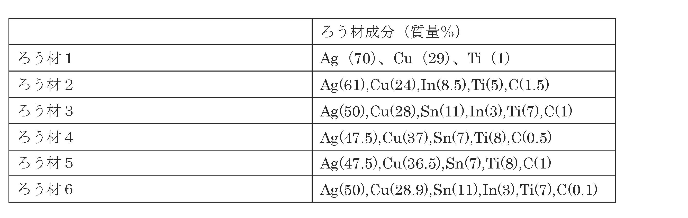
基板1として、例えば、表1に示す2つの基板が用いられる。
接合層3の材料として、例えば、表2に示す4つのろう材が用いられる。
金属部材2として、例えば、厚みが0.8mmの銅板が用いられる。基板1の上面及び下面にろう材ペーストを塗布する。ろう材ペーストの厚みは、25μmである。上面及び下面にそれぞれ金属部材を配置して接合する。上面に配置された金属部材をエッチング加工する。基板1と金属部材2を接合させる際の熱処理は、以下の7つの条件で実施される。
熱処理条件3~6では、基板1の温度を約600℃に保持したときの雰囲気、圧力、保持時間は、熱処理条件2と共通である。また、基板1の温度を700℃以上850℃以下に保持したときの雰囲気及び圧力は、熱処理条件2と共通である。熱処理条件7では、基板1の温度を850℃以上950℃以下に保持している。
(熱処理条件1)
1×10⁻³Pa以下の非酸化雰囲気中で、基板1の温度を700℃以上850℃以下に保持し、基板1を30分加熱する。非酸化雰囲気は、処理空間に存在する気体中の酸素濃度が25vol%以下であることを指す。
(熱処理条件2)
最初に、13.3Paの窒素雰囲気中で、基板1の温度を約500℃に保持し、基板1を30分加熱する。窒素雰囲気における窒素濃度は、90vol%である。次に、1×10⁻³Pa以下の非酸化雰囲気中で、基板1の温度を約600℃に保持し、基板1を120分加熱する。その後、1×10⁻³Pa以下の非酸化雰囲気中で、基板1の温度を700℃以上850℃以下に保持し、基板1を30分加熱する。
(熱処理条件3)
最初に、0.01Paの窒素雰囲気中で、基板1の温度を約500℃に保持し、基板1を30分加熱する。窒素雰囲気における窒素濃度は、99.9vol%である。次に、1×10⁻³Pa以下の非酸化雰囲気中で、約600℃で加熱後、基板1の温度を700℃以上850℃以下に保持し、基板1を30分加熱する。
(熱処理条件4)
最初に、0.5Paの窒素雰囲気中で、基板1の温度を約500℃に保持し、基板1を60分加熱する。窒素雰囲気における窒素濃度は、70vol%である。次に、1×10⁻³Pa以下の非酸化雰囲気中で、約600℃で加熱後、基板1の温度を700℃以上850℃以下に保持し、基板1を30分加熱する。
(熱処理条件5)
最初に、0.03Paの窒素雰囲気中で、基板1の温度を約500℃に保持し、基板1を120分加熱する。窒素雰囲気における窒素濃度は、80vol%である。次に、1×10⁻³Pa以下の非酸化雰囲気中で、約600℃で加熱後、基板1の温度を700℃以上850℃以下に保持し、基板1を120分加熱する。
(熱処理条件6)
最初に、5Paの窒素雰囲気中で、基板1の温度を約500℃に保持し、基板1を150分加熱する。窒素雰囲気における窒素濃度は、70vol%である。次に、1×10⁻³Pa以下の非酸化雰囲気中で、約600℃で加熱後、基板1の温度を700℃以上850℃以下に保持し、基板1を200分加熱する。
(熱処理条件7)
最初に、5Paの窒素雰囲気中で、基板1の温度を約500℃に保持し、基板1を150分加熱する。窒素雰囲気における窒素濃度は、90vol%である。次に、1×10⁻³Pa以下の非酸化雰囲気中で、約600℃で加熱後、基板1の温度を860℃以上950℃以下に保持し、基板1を100分加熱する。
熱処理条件3~6では、基板1の温度を約600℃に保持したときの雰囲気、圧力、保持時間は、熱処理条件2と共通である。また、基板1の温度を700℃以上850℃以下に保持したときの雰囲気及び圧力は、熱処理条件2と共通である。熱処理条件7では、基板1の温度を850℃以上950℃以下に保持している。
(熱処理条件1)
1×10⁻³Pa以下の非酸化雰囲気中で、基板1の温度を700℃以上850℃以下に保持し、基板1を30分加熱する。非酸化雰囲気は、処理空間に存在する気体中の酸素濃度が25vol%以下であることを指す。
(熱処理条件2)
最初に、13.3Paの窒素雰囲気中で、基板1の温度を約500℃に保持し、基板1を30分加熱する。窒素雰囲気における窒素濃度は、90vol%である。次に、1×10⁻³Pa以下の非酸化雰囲気中で、基板1の温度を約600℃に保持し、基板1を120分加熱する。その後、1×10⁻³Pa以下の非酸化雰囲気中で、基板1の温度を700℃以上850℃以下に保持し、基板1を30分加熱する。
(熱処理条件3)
最初に、0.01Paの窒素雰囲気中で、基板1の温度を約500℃に保持し、基板1を30分加熱する。窒素雰囲気における窒素濃度は、99.9vol%である。次に、1×10⁻³Pa以下の非酸化雰囲気中で、約600℃で加熱後、基板1の温度を700℃以上850℃以下に保持し、基板1を30分加熱する。
(熱処理条件4)
最初に、0.5Paの窒素雰囲気中で、基板1の温度を約500℃に保持し、基板1を60分加熱する。窒素雰囲気における窒素濃度は、70vol%である。次に、1×10⁻³Pa以下の非酸化雰囲気中で、約600℃で加熱後、基板1の温度を700℃以上850℃以下に保持し、基板1を30分加熱する。
(熱処理条件5)
最初に、0.03Paの窒素雰囲気中で、基板1の温度を約500℃に保持し、基板1を120分加熱する。窒素雰囲気における窒素濃度は、80vol%である。次に、1×10⁻³Pa以下の非酸化雰囲気中で、約600℃で加熱後、基板1の温度を700℃以上850℃以下に保持し、基板1を120分加熱する。
(熱処理条件6)
最初に、5Paの窒素雰囲気中で、基板1の温度を約500℃に保持し、基板1を150分加熱する。窒素雰囲気における窒素濃度は、70vol%である。次に、1×10⁻³Pa以下の非酸化雰囲気中で、約600℃で加熱後、基板1の温度を700℃以上850℃以下に保持し、基板1を200分加熱する。
(熱処理条件7)
最初に、5Paの窒素雰囲気中で、基板1の温度を約500℃に保持し、基板1を150分加熱する。窒素雰囲気における窒素濃度は、90vol%である。次に、1×10⁻³Pa以下の非酸化雰囲気中で、約600℃で加熱後、基板1の温度を860℃以上950℃以下に保持し、基板1を100分加熱する。
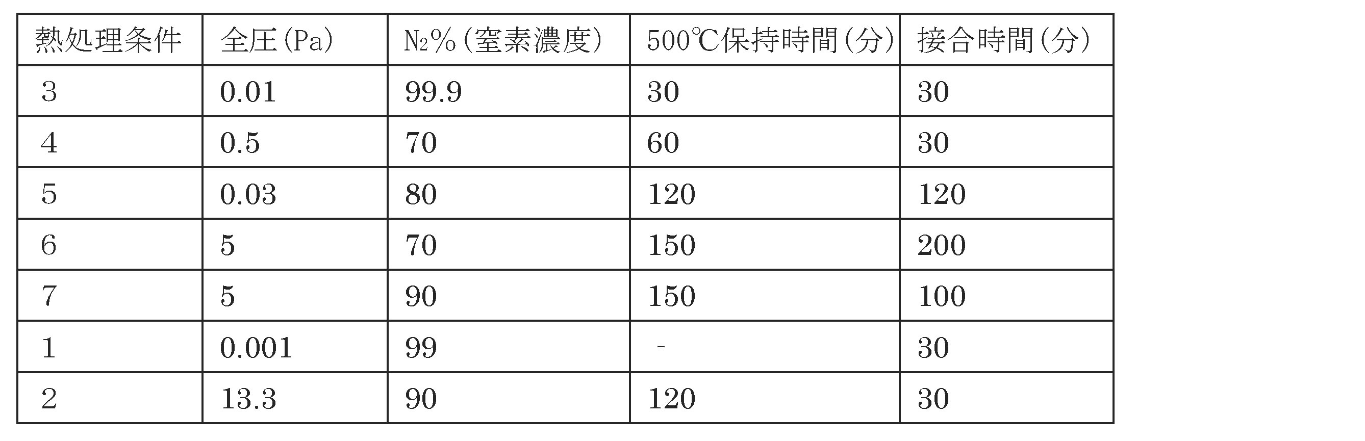
上述した各熱処理条件の概要を、表3に示す。
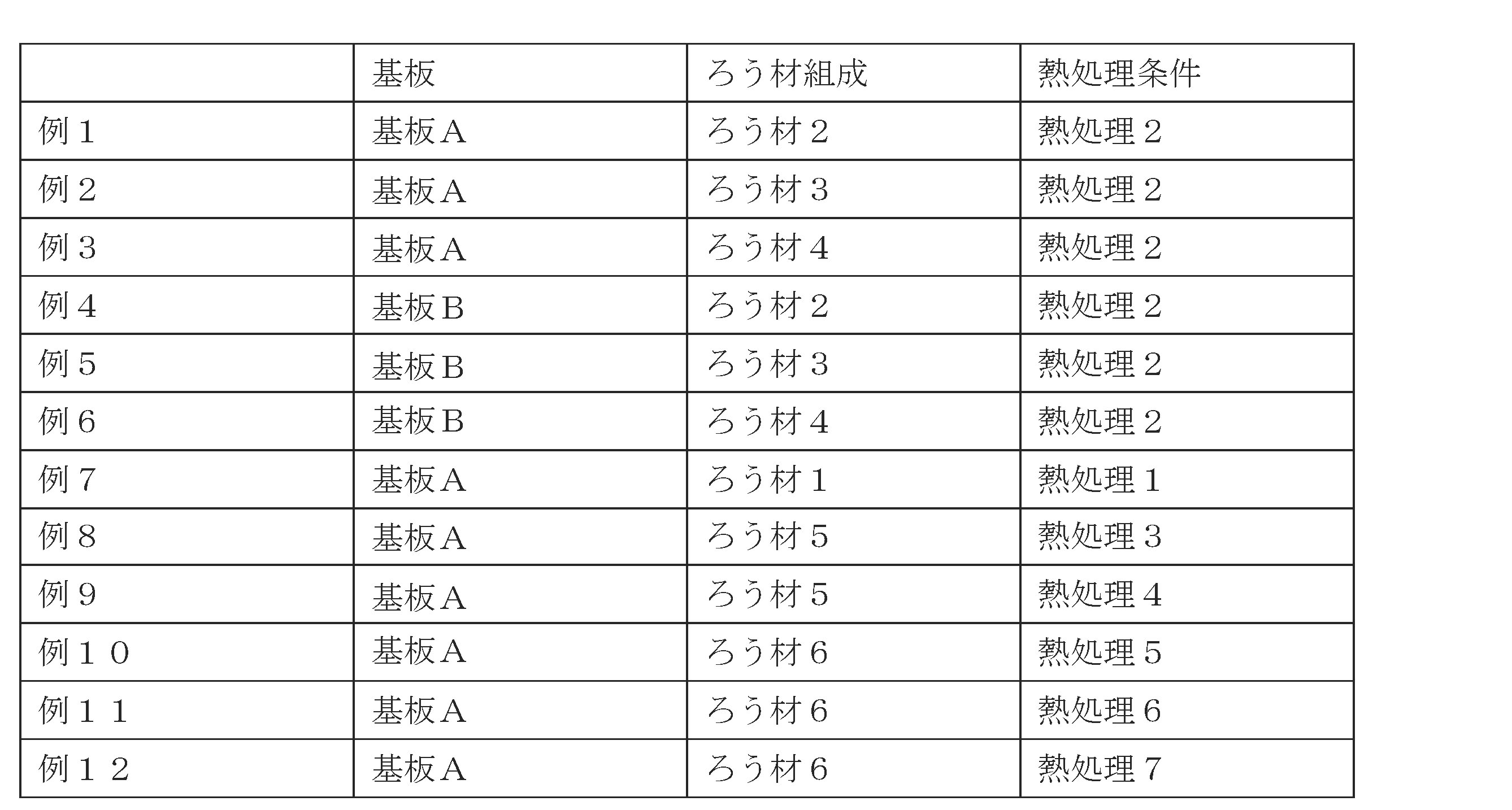
基板1の種類、ろう材の種類、及び熱処理条件の種類の組み合わせは、例えば表4に示す通りである。
それぞれの例に係る接合体について、ピール強度を測定し、且つTCTを行った。ピール強度は、基板1に1mm幅の金属部材2を接合し、金属部材2を垂直方向に引っ張ることで測定した。TCTでは、5000サイクル後の接合体における不具合の有無を測定した。1つのサイクルでは、-50℃で30分保持→室温で10分保持→200℃で30分保持→室温で10分保持を行なった。接合体における不具合は、超音波探傷装置(Scanning Acoustic Tomograph:SAT)により、基板1と金属部材2との間のクラック発生面積を求めた。クラック発生面積は、指数ηとして評価した。ηが100%の場合を「クラックなし」、0%の場合を「全面的にクラック発生」として示した。その結果を表5に示す。

表5の結果から、ろう材2~4のいずれかと熱処理条件2を用いたときは、ろう材1と熱処理条件1を用いたときに比べて、ピール強度を向上させ、クラックの発生を抑制できることが分かる。ろう材2~4は、ろう材1に比べて、炭素(C)をさらに含む。発明者らは、炭素が特性の向上に寄与していると推測した。発明者らは、この推測に基づき、接合層3において炭素を含む粒子に関する観察を行った。表6は、例1~7のそれぞれの接合層3の断面を電子顕微鏡により観察した結果を示す。粉体の数は、15μm×100μmの範囲を測定した。
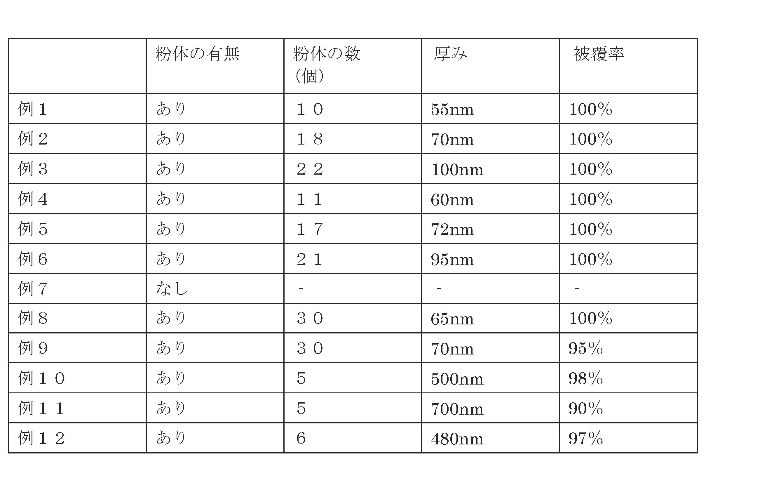
表6に示す厚みは、第2領域22の厚みを示す。第2領域22の厚みは、以下の方法で測定される。それぞれの第1粒子11の周りに存在する第2領域22の厚みを、第1粒子11から第1領域21に向かう一方向において測定する。方向は、無作為に決定される。それぞれの第2領域22の厚みは、次のように測定する。AMC断面を加工し、TEMで観察する。測定個所として、無作為に第2領域22を3か所選ぶ。測定個所の厚みを測定し、それらの平均値を「第2領域22の厚み」とする。
被覆率は、以下の方法で測定される。それぞれの第1粒子11について、外周の長さに対する、第2領域22と接する外周の長さの割合を計算する。それぞれの第1粒子11の割合を平均化し、「被覆率」とする。
表6に示す厚みは、第2領域22の厚みを示す。第2領域22の厚みは、以下の方法で測定される。それぞれの第1粒子11の周りに存在する第2領域22の厚みを、第1粒子11から第1領域21に向かう一方向において測定する。方向は、無作為に決定される。それぞれの第2領域22の厚みは、次のように測定する。AMC断面を加工し、TEMで観察する。測定個所として、無作為に第2領域22を3か所選ぶ。測定個所の厚みを測定し、それらの平均値を「第2領域22の厚み」とする。
被覆率は、以下の方法で測定される。それぞれの第1粒子11について、外周の長さに対する、第2領域22と接する外周の長さの割合を計算する。それぞれの第1粒子11の割合を平均化し、「被覆率」とする。
具体例に係る接合体の第2領域22を、STEM-EDSにより組成分析した。その結果、いずれの具体例においても、第2領域22におけるTi濃度は、50wt%以上であった。いずれの測定点からも、Ti、N、及びOが検出された。また、TEM像を観察すると、第2領域22は、微結晶の集合体であることが確認された。微結晶からは、炭素が検出された。
炭素を含むろう材を用いたとき、接合層3にて粉体10が確認される。すなわち、炭素を含む第1粒子11と、チタンを含む第2領域22が、接合層3に存在する。そして、第1粒子11は、第2領域22により囲まれている。このような構造の粉体10が設けられることで、接合体の強度が向上し、クラックの発生が抑制されると考えられる。
具体例に係る接合体の断面をSEMで観察した。それぞれの接合体の断面において、第1粒子11の長さLe1及びLe2を測定した。また、長さLe2に対する長さLe1の比(Le1/Le2)を計算した。長さLe1及びLe2の測定方法、及び長さLe2に対する長さLe1の比の計算方法は、上述した通りである。その結果を表7に示す。

表7から、具体例に係る接合体において、第1粒子11の長さLe2に対する長さLe1の比は、1.2以上40以下の範囲内であることが確認された。
表7から、具体例に係る接合体において、第1粒子11の長さLe2に対する長さLe1の比は、1.2以上40以下の範囲内であることが確認された。
以上で説明した各実施形態によれば、接合強度を向上できる接合体を提供できる。
本願明細書において、「垂直」及び「平行」は、厳密な垂直及び厳密な平行だけではなく、例えば製造工程におけるばらつきなどを含むものであり、実質的に垂直及び実質的に平行であれば良い。
以上、具体例を参照しつつ、本発明の実施の形態について説明した。しかし、本発明の実施形態は、これらの具体例に限定されるものではない。例えば、接合体に含まれる基板、金属部材、接合層などの各要素の具体的な構成に関しては、当業者が公知の範囲から適宜選択することにより本発明を同様に実施し、同様の効果を得ることができる限り、本発明の範囲に包含される。
また、各具体例のいずれか2つ以上の要素を技術的に可能な範囲で組み合わせたものも、本発明の要旨を包含する限り本発明の範囲に含まれる。
その他、本発明の実施の形態として上述した接合体を基にして、当業者が適宜設計変更して実施し得る全ての接合体も、本発明の要旨を包含する限り、本発明の範囲に属する。
その他、本発明の思想の範疇において、当業者であれば、各種の変更例及び修正例に想到し得るものであり、それら変更例及び修正例についても本発明の範囲に属するものと了解される。
本発明のいくつかの実施形態を説明したが、これらの実施形態は、例として提示したものであり、発明の範囲を限定することは意図していない。これら新規な実施形態は、その他の様々な形態で実施されることが可能であり、発明の要旨を逸脱しない範囲で、種々の省略、置き換え、変更を行うことができる。これら実施形態やその変形は、発明の範囲や要旨に含まれるとともに、請求の範囲に記載された発明とその均等の範囲に含まれる。
1 基板、 2 金属部材、 2S 側面、 2U 上面、 2a~2d 金属部材、 3 接合層、 3J はみ出し部、 3a~3c 接合層、 4a,4b 接続部、 5 半導体素子、 6a,6b 接合層、 7 ボンディングワイヤ、 8 金属端子、 10 粉体、 11 第1粒子、 12 第2粒子、 13 第3粒子、 21 第1領域、 21a 第1部分領域、 21b 第2部分領域、 22 第2領域、 23 第3領域、 24 第4領域、 θ1 傾斜角度、 θ2 角度、 100~120 接合体、 210 半導体装置、 CL 中心線、 CS 接触面、 D1 第1方向、 D2 第2方向、 D3 第3方向、 D4 第4方向、 IS 交点、 L 層、 L1 第1層、 L2 第2層、 Le1,Le2 長さ、 S1 第1面、 S2 第2面、 T 厚み、 W 長さ
Claims (21)
- 基板と、
金属部材と、
前記基板と前記金属部材との間に設けられた接合層であって、
炭素を含む第1粒子と、
金属を含む第1領域と、
チタンを含み、前記第1粒子と前記第1領域との間に設けられた第2領域と、
を含み、前記第2領域におけるチタンの濃度は前記第1領域におけるチタンの濃度よりも高い、前記接合層と、
を備えた接合体。 - 前記第2領域におけるチタンの濃度は、前記第1粒子におけるチタンの濃度よりも高い請求項1記載の接合体。
- 前記第2領域におけるチタンの含有率は、50質量%以上である請求項1又は2に記載の接合体。
- 前記第2領域は、前記第1粒子の周りに設けられ、
前記第2領域は、複数の第2粒子を含み、
前記複数の第2粒子の少なくとも1つは、チタンを含む請求項1~3のいずれか1つに記載の接合体。 - 前記複数の第2粒子の1つの大きさは、前記第1粒子の大きさよりも小さい請求項4記載の接合体。
- 前記複数の第2粒子の前記少なくとも1つは、チタン及び窒素を含む請求項4又は5に記載の接合体。
- 前記複数の第2粒子の前記少なくとも1つは、チタンと、窒素及び酸素からなる群より選択された少なくとも1つと、の結晶を含む請求項4又は5に記載の接合体。
- 前記第2領域の厚みは、2nm以上1μm以下である請求項1~7のいずれか1つに記載の接合体。
- 前記第1粒子及び前記第2領域を含む粉体が複数設けられ、
複数の前記粉体の少なくとも2つは、互いに離れている請求項1~8のいずれか1つに記載の接合体。 - 前記第1粒子は、第1結晶層を含み、
前記第1結晶層は、炭素を含む請求項1~9のいずれか1つに記載の接合体。 - 前記第1結晶層は、第1方向に沿って設けられ、
前記第1方向における前記第1粒子の長さは、前記第1方向と交差する第2方向における前記第1粒子の長さよりも長い請求項10記載の接合体。 - 前記第1方向における前記第1粒子の前記長さは、前記第2方向における前記第1粒子の前記長さの1.2倍以上40倍以下である請求項11記載の接合体。
- 前記第1領域は、銀を含む第1部分領域と、銅を含む第2部分領域と、を含む請求項1~12のいずれか1つに記載の接合体。
- 前記第2領域は、前記第1部分領域と接する請求項13記載の接合体。
- 前記第1粒子の中に、前記金属を含む第3領域が設けられた請求項1~14のいずれか1つに記載の接合体。
- 前記第1粒子は、炭素を含む第1層と、炭素を含む第2層と、を含み、
前記第1層と前記第2層との間に、前記金属を含む第3領域が設けられた請求項1~9のいずれか1つに記載の接合体。 - 前記第3領域は、前記基板に含まれる元素と同じ種類の元素を少なくとも1つ含む請求項16記載の接合体。
- 前記接合層は、第4領域をさらに含み、
前記第4領域は、チタン及び窒素を含み、
前記第4領域は、前記基板と前記第1領域との間に位置する請求項1~17のいずれか1つに記載の接合体。 - 前記基板は、珪素及び窒素を含み、
前記金属部材は、銅を含む請求項1~18のいずれか1つに記載の接合体。 - 請求項1~19のいずれか1つに記載の接合体を備えた回路基板。
- 請求項20に記載の回路基板と、
前記回路基板に搭載された半導体素子と、
を備えた半導体装置。
Priority Applications (5)
| Application Number | Priority Date | Filing Date | Title |
|---|---|---|---|
| CN202080018277.0A CN113508462B (zh) | 2019-09-02 | 2020-08-20 | 接合体、电路基板及半导体装置 |
| EP20861301.8A EP4026819A4 (en) | 2019-09-02 | 2020-08-20 | COMPOSITE BODY, CIRCUIT BOARD AND SEMICONDUCTOR COMPONENT |
| JP2021543688A JP7240511B2 (ja) | 2019-09-02 | 2020-08-20 | 接合体 |
| US17/446,765 US11948900B2 (en) | 2019-09-02 | 2021-09-02 | Bonded body, circuit board, and semiconductor device |
| JP2022188028A JP7471376B2 (ja) | 2019-09-02 | 2022-11-25 | 回路基板及び半導体装置 |
Applications Claiming Priority (2)
| Application Number | Priority Date | Filing Date | Title |
|---|---|---|---|
| JP2019-159468 | 2019-09-02 | ||
| JP2019159468 | 2019-09-02 |
Related Child Applications (1)
| Application Number | Title | Priority Date | Filing Date |
|---|---|---|---|
| US17/446,765 Continuation US11948900B2 (en) | 2019-09-02 | 2021-09-02 | Bonded body, circuit board, and semiconductor device |
Publications (1)
| Publication Number | Publication Date |
|---|---|
| WO2021044854A1 true WO2021044854A1 (ja) | 2021-03-11 |
Family
ID=74852458
Family Applications (1)
| Application Number | Title | Priority Date | Filing Date |
|---|---|---|---|
| PCT/JP2020/031407 Ceased WO2021044854A1 (ja) | 2019-09-02 | 2020-08-20 | 接合体、回路基板、及び半導体装置 |
Country Status (5)
| Country | Link |
|---|---|
| US (1) | US11948900B2 (ja) |
| EP (1) | EP4026819A4 (ja) |
| JP (2) | JP7240511B2 (ja) |
| CN (1) | CN113508462B (ja) |
| WO (1) | WO2021044854A1 (ja) |
Cited By (2)
| Publication number | Priority date | Publication date | Assignee | Title |
|---|---|---|---|---|
| WO2023286858A1 (ja) * | 2021-07-16 | 2023-01-19 | 三菱マテリアル株式会社 | 銅/セラミックス接合体、絶縁回路基板、および、銅/セラミックス接合体の製造方法、絶縁回路基板の製造方法 |
| US20250010408A1 (en) * | 2023-07-06 | 2025-01-09 | Tong Hsing Electronic Industries, Ltd. | Active metal brazing substrate material containing aluminum metal element and method for producing the same |
Families Citing this family (4)
| Publication number | Priority date | Publication date | Assignee | Title |
|---|---|---|---|---|
| CN113508462B (zh) * | 2019-09-02 | 2024-09-20 | 株式会社东芝 | 接合体、电路基板及半导体装置 |
| WO2021111508A1 (ja) * | 2019-12-03 | 2021-06-10 | 日本碍子株式会社 | 接合基板及び接合基板の製造方法 |
| EP4715306A1 (en) | 2023-05-19 | 2026-03-25 | Niterra Materials Co., Ltd. | Heat treatment furnace device |
| JP7734345B1 (ja) | 2024-02-20 | 2025-09-05 | 株式会社Niterra Materials | セラミックス封着部品およびその製造方法 |
Citations (11)
| Publication number | Priority date | Publication date | Assignee | Title |
|---|---|---|---|---|
| JPH05148053A (ja) * | 1991-11-29 | 1993-06-15 | Toshiba Corp | セラミツクス−金属接合体 |
| JPH05319946A (ja) * | 1992-05-22 | 1993-12-03 | Ibiden Co Ltd | 金属板接合セラミック基板 |
| JPH10158073A (ja) * | 1996-11-25 | 1998-06-16 | Sumitomo Kinzoku Erekutorodebaisu:Kk | セラミックス基板と金属板との接合方法 |
| CN101148365A (zh) * | 2007-09-11 | 2008-03-26 | 西安交通大学 | 一种ZrO2陶瓷与不锈钢或Al2O3陶瓷无压钎焊的方法 |
| CN101468799A (zh) * | 2007-09-11 | 2009-07-01 | 西安交通大学 | 一种ZrO2陶瓷与Al2O3陶瓷无压钎焊的方法 |
| WO2010137651A1 (ja) * | 2009-05-27 | 2010-12-02 | 京セラ株式会社 | ろう材およびこれを用いた放熱基体ならびに電子装置 |
| WO2011034075A1 (ja) | 2009-09-15 | 2011-03-24 | 株式会社 東芝 | セラミックス回路基板及びその製造方法 |
| JP2012115846A (ja) * | 2010-11-29 | 2012-06-21 | Kyocera Corp | ろう材およびこれを用いた回路基板ならびに電子装置 |
| WO2015019602A1 (ja) * | 2013-08-08 | 2015-02-12 | 株式会社 東芝 | 回路基板および半導体装置 |
| JP2015092552A (ja) * | 2013-09-30 | 2015-05-14 | 三菱マテリアル株式会社 | Cu/セラミックス接合体、Cu/セラミックス接合体の製造方法、及び、パワーモジュール用基板 |
| WO2018021472A1 (ja) | 2016-07-28 | 2018-02-01 | 株式会社 東芝 | 接合体、回路基板、および半導体装置 |
Family Cites Families (17)
| Publication number | Priority date | Publication date | Assignee | Title |
|---|---|---|---|---|
| JP4077888B2 (ja) * | 1995-07-21 | 2008-04-23 | 株式会社東芝 | セラミックス回路基板 |
| JP3834351B2 (ja) | 1996-04-09 | 2006-10-18 | 株式会社東芝 | セラミックス回路基板 |
| JP4574951B2 (ja) * | 2003-02-26 | 2010-11-04 | 株式会社東芝 | 半導体装置及びその製造方法 |
| US9425146B2 (en) * | 2010-09-28 | 2016-08-23 | Infineon Technologies Ag | Semiconductor structure and method for making same |
| CN102893419A (zh) * | 2010-10-29 | 2013-01-23 | 铼钻科技股份有限公司 | 应力被调节的半导体装置及其相关方法 |
| EP2689881B1 (en) * | 2011-03-25 | 2019-10-16 | NGK Insulators, Ltd. | Bonded object of tungsten carbide-based superhard alloy and process for producing same |
| JP5472529B2 (ja) * | 2011-03-31 | 2014-04-16 | 日立ツール株式会社 | 硬質皮膜被覆部材及びそれを具備する刃先交換式回転工具 |
| KR101659194B1 (ko) * | 2011-12-20 | 2016-09-22 | 가부시끼가이샤 도시바 | 세라믹 구리 회로 기판과 그것을 사용한 반도체 장치 |
| JP2014118310A (ja) * | 2012-12-14 | 2014-06-30 | Denki Kagaku Kogyo Kk | セラミックス回路基板 |
| WO2015072250A1 (ja) * | 2013-11-15 | 2015-05-21 | 住友電工ハードメタル株式会社 | ダイヤモンド接合体、それを備える工具、およびダイヤモンド接合体の製造方法 |
| US10424529B2 (en) | 2014-02-21 | 2019-09-24 | Denka Company Limited | Ceramic circuit board |
| JP5972317B2 (ja) * | 2014-07-15 | 2016-08-17 | 株式会社マテリアル・コンセプト | 電子部品およびその製造方法 |
| JP6307386B2 (ja) | 2014-08-20 | 2018-04-04 | デンカ株式会社 | セラミックス回路基板 |
| JP6799790B2 (ja) * | 2016-12-06 | 2020-12-16 | パナソニックIpマネジメント株式会社 | 接合材とそれにより得られる接合体と接合体の製造方法 |
| JP6965768B2 (ja) * | 2017-02-28 | 2021-11-10 | 三菱マテリアル株式会社 | 銅/セラミックス接合体、絶縁回路基板、及び、銅/セラミックス接合体の製造方法、絶縁回路基板の製造方法 |
| US10629686B2 (en) * | 2018-08-02 | 2020-04-21 | Semiconductor Components Industries, Llc | Carbon-controlled ohmic contact layer for backside ohmic contact on a silicon carbide power semiconductor device |
| CN113508462B (zh) | 2019-09-02 | 2024-09-20 | 株式会社东芝 | 接合体、电路基板及半导体装置 |
-
2020
- 2020-08-20 CN CN202080018277.0A patent/CN113508462B/zh active Active
- 2020-08-20 EP EP20861301.8A patent/EP4026819A4/en active Pending
- 2020-08-20 WO PCT/JP2020/031407 patent/WO2021044854A1/ja not_active Ceased
- 2020-08-20 JP JP2021543688A patent/JP7240511B2/ja active Active
-
2021
- 2021-09-02 US US17/446,765 patent/US11948900B2/en active Active
-
2022
- 2022-11-25 JP JP2022188028A patent/JP7471376B2/ja active Active
Patent Citations (11)
| Publication number | Priority date | Publication date | Assignee | Title |
|---|---|---|---|---|
| JPH05148053A (ja) * | 1991-11-29 | 1993-06-15 | Toshiba Corp | セラミツクス−金属接合体 |
| JPH05319946A (ja) * | 1992-05-22 | 1993-12-03 | Ibiden Co Ltd | 金属板接合セラミック基板 |
| JPH10158073A (ja) * | 1996-11-25 | 1998-06-16 | Sumitomo Kinzoku Erekutorodebaisu:Kk | セラミックス基板と金属板との接合方法 |
| CN101148365A (zh) * | 2007-09-11 | 2008-03-26 | 西安交通大学 | 一种ZrO2陶瓷与不锈钢或Al2O3陶瓷无压钎焊的方法 |
| CN101468799A (zh) * | 2007-09-11 | 2009-07-01 | 西安交通大学 | 一种ZrO2陶瓷与Al2O3陶瓷无压钎焊的方法 |
| WO2010137651A1 (ja) * | 2009-05-27 | 2010-12-02 | 京セラ株式会社 | ろう材およびこれを用いた放熱基体ならびに電子装置 |
| WO2011034075A1 (ja) | 2009-09-15 | 2011-03-24 | 株式会社 東芝 | セラミックス回路基板及びその製造方法 |
| JP2012115846A (ja) * | 2010-11-29 | 2012-06-21 | Kyocera Corp | ろう材およびこれを用いた回路基板ならびに電子装置 |
| WO2015019602A1 (ja) * | 2013-08-08 | 2015-02-12 | 株式会社 東芝 | 回路基板および半導体装置 |
| JP2015092552A (ja) * | 2013-09-30 | 2015-05-14 | 三菱マテリアル株式会社 | Cu/セラミックス接合体、Cu/セラミックス接合体の製造方法、及び、パワーモジュール用基板 |
| WO2018021472A1 (ja) | 2016-07-28 | 2018-02-01 | 株式会社 東芝 | 接合体、回路基板、および半導体装置 |
Non-Patent Citations (1)
| Title |
|---|
| See also references of EP4026819A4 |
Cited By (3)
| Publication number | Priority date | Publication date | Assignee | Title |
|---|---|---|---|---|
| WO2023286858A1 (ja) * | 2021-07-16 | 2023-01-19 | 三菱マテリアル株式会社 | 銅/セラミックス接合体、絶縁回路基板、および、銅/セラミックス接合体の製造方法、絶縁回路基板の製造方法 |
| US12550731B2 (en) | 2021-07-16 | 2026-02-10 | Mitsubishi Materials Corporation | Copper/ceramic assembly, insulating circuit substrate, production method for copper/ceramic assembly, and production method for insulating circuit substrate |
| US20250010408A1 (en) * | 2023-07-06 | 2025-01-09 | Tong Hsing Electronic Industries, Ltd. | Active metal brazing substrate material containing aluminum metal element and method for producing the same |
Also Published As
| Publication number | Publication date |
|---|---|
| JP2023052728A (ja) | 2023-04-12 |
| CN113508462A (zh) | 2021-10-15 |
| EP4026819A1 (en) | 2022-07-13 |
| JP7471376B2 (ja) | 2024-04-19 |
| EP4026819A4 (en) | 2023-12-06 |
| US20210398928A1 (en) | 2021-12-23 |
| CN113508462B (zh) | 2024-09-20 |
| JPWO2021044854A1 (ja) | 2021-03-11 |
| US11948900B2 (en) | 2024-04-02 |
| JP7240511B2 (ja) | 2023-03-15 |
Similar Documents
| Publication | Publication Date | Title |
|---|---|---|
| JP7240511B2 (ja) | 接合体 | |
| KR102459745B1 (ko) | 구리/세라믹스 접합체, 절연 회로 기판, 및, 구리/세라믹스 접합체의 제조 방법, 절연 회로 기판의 제조 방법 | |
| JP5226511B2 (ja) | セラミックス−金属接合体、その製造方法およびそれを用いた半導体装置 | |
| JP6908173B2 (ja) | 銅/セラミックス接合体、絶縁回路基板、及び、銅/セラミックス接合体の製造方法、絶縁回路基板の製造方法 | |
| CN113597674A (zh) | 陶瓷铜电路基板及使用了其的半导体装置 | |
| WO2021112060A1 (ja) | 銅/セラミックス接合体、絶縁回路基板、及び、銅/セラミックス接合体の製造方法、絶縁回路基板の製造方法 | |
| JPWO2015182385A1 (ja) | ヒートスプレッダ | |
| WO2023008562A1 (ja) | 銅/セラミックス接合体、および、絶縁回路基板 | |
| JP2008198706A (ja) | 回路基板、その製造方法およびそれを用いた半導体モジュール | |
| WO2024195792A1 (ja) | 静電チャック装置 | |
| JP7563124B2 (ja) | グラフェン接合体 | |
| JP6928297B2 (ja) | 銅/セラミックス接合体、及び、絶縁回路基板 | |
| EP4053091A1 (en) | Copper/ceramic assembly, insulated circuit board, method for producing copper/ceramic assembly, and method for producing insulated circuit board | |
| WO2021044844A1 (ja) | 銅/セラミックス接合体、及び、絶縁回路基板 | |
| JP6893593B2 (ja) | Niナノ粒子を用いた接合材料及び接合構造体 | |
| JPH1180858A (ja) | 複合材料及びその製造方法 | |
| JP4557398B2 (ja) | 電子素子 | |
| JP4919357B2 (ja) | 電子デバイスの製造方法 | |
| JPH08274423A (ja) | セラミックス回路基板 | |
| WO2021117327A1 (ja) | 銅/セラミックス接合体、及び、絶縁回路基板 | |
| WO2021106904A1 (ja) | グラフェン接合体 | |
| JP7540345B2 (ja) | 銅/セラミックス接合体、および、絶縁回路基板 | |
| WO2021090759A1 (ja) | グラフェン含有炭素質部材/セラミックス接合体、および、銅/グラフェン含有炭素質部材/セラミックス接合体 | |
| JP2020132909A (ja) | 接合用ペースト、接合構造体および接合方法 | |
| JP7663041B2 (ja) | 銅/セラミックス接合体、および、絶縁回路基板 |
Legal Events
| Date | Code | Title | Description |
|---|---|---|---|
| 121 | Ep: the epo has been informed by wipo that ep was designated in this application |
Ref document number: 20861301 Country of ref document: EP Kind code of ref document: A1 |
|
| ENP | Entry into the national phase |
Ref document number: 2021543688 Country of ref document: JP Kind code of ref document: A |
|
| NENP | Non-entry into the national phase |
Ref country code: DE |
|
| ENP | Entry into the national phase |
Ref document number: 2020861301 Country of ref document: EP Effective date: 20220404 |