WO2021063052A1 - 漏电补偿动态寄存器、数据运算单元、芯片、算力板及计算设备 - Google Patents
漏电补偿动态寄存器、数据运算单元、芯片、算力板及计算设备 Download PDFInfo
- Publication number
- WO2021063052A1 WO2021063052A1 PCT/CN2020/098902 CN2020098902W WO2021063052A1 WO 2021063052 A1 WO2021063052 A1 WO 2021063052A1 CN 2020098902 W CN2020098902 W CN 2020098902W WO 2021063052 A1 WO2021063052 A1 WO 2021063052A1
- Authority
- WO
- WIPO (PCT)
- Prior art keywords
- terminal
- leakage compensation
- unit
- electrically connected
- data
- Prior art date
- Legal status (The legal status is an assumption and is not a legal conclusion. Google has not performed a legal analysis and makes no representation as to the accuracy of the status listed.)
- Ceased
Links
Images



Classifications
-
- G—PHYSICS
- G11—INFORMATION STORAGE
- G11C—STATIC STORES
- G11C19/00—Digital stores in which the information is moved stepwise, e.g. shift registers
- G11C19/28—Digital stores in which the information is moved stepwise, e.g. shift registers using semiconductor elements
- G11C19/287—Organisation of a multiplicity of shift registers
-
- G—PHYSICS
- G11—INFORMATION STORAGE
- G11C—STATIC STORES
- G11C19/00—Digital stores in which the information is moved stepwise, e.g. shift registers
- G11C19/28—Digital stores in which the information is moved stepwise, e.g. shift registers using semiconductor elements
-
- H—ELECTRICITY
- H03—ELECTRONIC CIRCUITRY
- H03K—PULSE TECHNIQUE
- H03K19/00—Logic circuits, i.e. having at least two inputs acting on one output; Inverting circuits
- H03K19/003—Modifications for increasing the reliability for protection
- H03K19/00346—Modifications for eliminating interference or parasitic voltages or currents
- H03K19/00361—Modifications for eliminating interference or parasitic voltages or currents in field effect transistor circuits
-
- G—PHYSICS
- G06—COMPUTING OR CALCULATING; COUNTING
- G06F—ELECTRIC DIGITAL DATA PROCESSING
- G06F15/00—Digital computers in general; Data processing equipment in general
- G06F15/76—Architectures of general purpose stored program computers
- G06F15/78—Architectures of general purpose stored program computers comprising a single central processing unit
- G06F15/7828—Architectures of general purpose stored program computers comprising a single central processing unit without memory
- G06F15/7832—Architectures of general purpose stored program computers comprising a single central processing unit without memory on one IC chip (single chip microprocessors)
-
- H—ELECTRICITY
- H03—ELECTRONIC CIRCUITRY
- H03K—PULSE TECHNIQUE
- H03K19/00—Logic circuits, i.e. having at least two inputs acting on one output; Inverting circuits
- H03K19/02—Logic circuits, i.e. having at least two inputs acting on one output; Inverting circuits using specified components
- H03K19/173—Logic circuits, i.e. having at least two inputs acting on one output; Inverting circuits using specified components using elementary logic circuits as components
- H03K19/177—Logic circuits, i.e. having at least two inputs acting on one output; Inverting circuits using specified components using elementary logic circuits as components arranged in matrix form
- H03K19/17704—Logic circuits, i.e. having at least two inputs acting on one output; Inverting circuits using specified components using elementary logic circuits as components arranged in matrix form the logic functions being realised by the interconnection of rows and columns
- H03K19/17708—Logic circuits, i.e. having at least two inputs acting on one output; Inverting circuits using specified components using elementary logic circuits as components arranged in matrix form the logic functions being realised by the interconnection of rows and columns using an AND matrix followed by an OR matrix, i.e. programmable logic arrays
- H03K19/17716—Logic circuits, i.e. having at least two inputs acting on one output; Inverting circuits using specified components using elementary logic circuits as components arranged in matrix form the logic functions being realised by the interconnection of rows and columns using an AND matrix followed by an OR matrix, i.e. programmable logic arrays with synchronous operation, i.e. using clock signals, e.g. of I/O or coupling register
-
- H—ELECTRICITY
- H03—ELECTRONIC CIRCUITRY
- H03K—PULSE TECHNIQUE
- H03K19/00—Logic circuits, i.e. having at least two inputs acting on one output; Inverting circuits
- H03K19/02—Logic circuits, i.e. having at least two inputs acting on one output; Inverting circuits using specified components
- H03K19/173—Logic circuits, i.e. having at least two inputs acting on one output; Inverting circuits using specified components using elementary logic circuits as components
- H03K19/177—Logic circuits, i.e. having at least two inputs acting on one output; Inverting circuits using specified components using elementary logic circuits as components arranged in matrix form
- H03K19/1778—Structural details for adapting physical parameters
- H03K19/17784—Structural details for adapting physical parameters for supply voltage
-
- H—ELECTRICITY
- H03—ELECTRONIC CIRCUITRY
- H03K—PULSE TECHNIQUE
- H03K3/00—Circuits for generating electric pulses; Monostable, bistable or multistable circuits
- H03K3/02—Generators characterised by the type of circuit or by the means used for producing pulses
- H03K3/353—Generators characterised by the type of circuit or by the means used for producing pulses by the use, as active elements, of field-effect transistors with internal or external positive feedback
- H03K3/356—Bistable circuits
- H03K3/356104—Bistable circuits using complementary field-effect transistors
- H03K3/356113—Bistable circuits using complementary field-effect transistors using additional transistors in the input circuit
- H03K3/356147—Bistable circuits using complementary field-effect transistors using additional transistors in the input circuit using pass gates
Definitions
- the invention relates to a storage device controlled by a clock, in particular to a leakage compensation dynamic register, a data operation unit, a chip, a computing power board and a computing device used in a large-scale data computing device.
- FIG. 1 is a circuit structure diagram of an existing dynamic register.
- the dynamic register includes a transmission gate 101, a tri-state inverter 102, and an inverter 103 connected in series between an input terminal D and an output terminal Q.
- a node S0 is formed between the transmission gate 101 and the three-state inverter 102
- a node S1 is formed between the three-state inverter 102 and the inverter 103.
- the data passes through the three-state inverter 102 and the parasitic of the transistor in the inverter 103.
- the capacitor temporarily exists at node S0 and/or node S1. However, the node S0 is prone to dynamic leakage, resulting in the loss of temporarily stored data.
- the present invention provides a leakage compensation dynamic register, which can effectively compensate the dynamic leakage current of the node and improve the safety and accuracy of data.
- the present invention provides a leakage compensation dynamic register, which includes an input terminal for inputting a piece of data; an output terminal for outputting the data; a clock signal terminal for providing a clock signal; an analog A switch unit, which transmits the data under the control of the clock signal; a data latch unit, which latches the data under the control of the clock signal; an output drive unit, which is used to invert and output the data latch
- the data received by the storage unit; the analog switch unit, the data latch unit, and the output drive unit are sequentially connected in series between the input terminal and the output terminal, and the analog switch unit and the output There is a node between the data latch units; wherein, a leakage compensation unit is further included, and the leakage compensation unit is electrically connected between the node and the output terminal.
- the leakage compensation unit has a first terminal, a second terminal, and a control terminal.
- the first terminal is electrically connected to the output terminal, and the second terminal is electrically connected to the output terminal. Connect to the node.
- the leakage compensation unit includes a PMOS transistor and an NMOS transistor, and the PMOS transistor and the NMOS transistor are connected in series between the output terminal and the node.
- the above-mentioned leakage compensation dynamic register wherein the PMOS transistor has a source terminal, a drain terminal and a gate terminal, the NMOS transistor has a source terminal, a drain terminal and a gate terminal, and the PMOS transistor The source terminal is electrically connected to the output terminal, the drain terminal is electrically connected to the drain terminal of the NMOS transistor, and the source terminal of the NMOS transistor is electrically connected to the node.
- the PMOS transistor is connected in parallel with the gate terminal of the NMOS transistor and electrically connected to a power source.
- the PMOS transistor is connected in parallel with the gate terminal of the NMOS transistor and electrically connected to the node.
- the above-mentioned leakage compensation dynamic register wherein the PMOS transistor has a source terminal, a drain terminal and a gate terminal, the NMOS transistor has a source terminal, a drain terminal and a gate terminal, and the NMOS transistor The source terminal is electrically connected to the output terminal, the drain terminal is electrically connected to the drain terminal of the PMOS transistor, and the source terminal of the PMOS transistor is electrically connected to the node.
- the PMOS transistor is connected in parallel with the gate terminal of the NMOS transistor and electrically connected to a ground.
- the PMOS transistor is connected in parallel with the gate terminal of the NMOS transistor and electrically connected to the node.
- the leakage compensation unit includes a PMOS transistor, the PMOS transistor has a source terminal, a drain terminal, and a gate terminal, and the source terminal of the PMOS transistor is electrically connected to the PMOS transistor.
- the drain terminal is electrically connected to the node, and the gate terminal is electrically connected to a power source.
- the leakage compensation unit includes an NMOS transistor, the NMOS transistor has a source terminal, a drain terminal, and a gate terminal, and the drain terminal of the NMOS transistor is electrically connected to the NMOS transistor.
- the source terminal is electrically connected to the node
- the gate terminal is electrically connected to a ground.
- the clock signal includes a first clock signal and a second clock signal, and the first clock signal is inverted from the second clock signal.
- the analog switch unit is a transmission gate.
- the data latch unit is a three-state inverter.
- the output driving unit is an inverter.
- the leakage compensation dynamic register of the present invention By using the leakage compensation dynamic register of the present invention, the leakage current can be fed back to the node from the output end, the dynamic leakage current of the node can be compensated, the stability of data storage can be improved, and the safety and accuracy of the data can be enhanced.
- the present invention also provides a data operation unit, including a control circuit, an arithmetic circuit, and a plurality of leakage compensation dynamic registers that are interconnected, and the plurality of leakage compensation dynamic registers are connected in series and/or in parallel. Connection; wherein, the multiple leakage compensation dynamic registers are any of the above-mentioned leakage compensation dynamic registers.
- the present invention also provides a chip, which includes at least one data operation unit described above.
- the present invention also provides a computing power board for computing equipment, which includes at least one of the above-mentioned chips.
- the present invention also provides a computing device, including a power supply board, a control board, a connecting board, a heat sink, and a plurality of computing power boards.
- the control board communicates with the computing power board through the connecting board.
- the power board is connected, the heat sink is arranged around the power board, and the power board is used to provide power to the connection board, the control board, the heat sink, and the power board, wherein:
- the hashrate board is the aforementioned hashrate board.
- Figure 1 is a schematic diagram of the circuit structure of an existing dynamic register
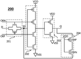
- FIG. 2 is a schematic diagram of a circuit structure of a leakage compensation dynamic register according to an embodiment of the present invention
- FIG. 3 is a schematic diagram of a circuit structure of a leakage compensation dynamic register according to another embodiment of the present invention.
- FIG. 4 is a schematic diagram of the circuit structure of a leakage compensation dynamic register according to another embodiment of the present invention.
- FIG. 5 is a schematic diagram of the circuit structure of a leakage compensation dynamic register according to another embodiment of the present invention.
- FIG. 6 is a schematic diagram of the circuit structure of a leakage compensation dynamic register according to an extended embodiment of the present invention.
- FIG. 7 is a schematic diagram of the circuit structure of a leakage compensation dynamic register according to another extended embodiment of the present invention.
- FIG. 8 is a schematic diagram of the structure of the data operation unit of the present invention.
- Figure 9 is a schematic diagram of the structure of the chip of the present invention.
- Figure 10 is a schematic diagram of the structure of the hash board of the present invention.
- FIG. 11 is a schematic diagram of the structure of the computing device of the present invention.
- 201P, 202P1, 202P2, 204P PMOS transistor
- 201N, 202N1, 202N2, 204N NMOS transistor
- connection here includes any direct and indirect electrical connection means. Indirect electrical connection means include connection through other devices.
- the leakage compensation dynamic register 200 includes an input terminal D, an output terminal Q, a clock signal terminal CKN, a clock signal terminal CKP, an analog switch unit 201, a data latch unit 202, an output drive unit 203, and a leakage compensation unit 204 .
- the analog switch unit 201, the data latch unit 202, and the output drive unit 203 are sequentially connected in series between the input terminal D and the output terminal Q, and a node S0 is formed between the analog switch unit 201 and the data latch unit 202.
- the leakage compensation unit 204 is electrically connected between the node S0 and the output terminal Q.
- the input terminal D is used to input data
- the output terminal is used to output data
- the clock signal terminal CKN and the clock signal terminal CKP are used to provide a clock signal CKN and a clock signal CKP
- the clock signal CKN and the clock signal CKP are inverted clock signals.
- the analog switch unit 201 of the leakage compensation dynamic register 200 has a transmission gate structure, and the analog switch unit 201 includes a PMOS transistor 201P and an NMOS transistor 201N connected in parallel.
- the source terminal of the PMOS transistor 201P is connected in parallel with the source terminal of the NMOS transistor 201N, and is electrically connected to the input terminal D
- the drain terminal of the PMOS transistor 201P is connected in parallel with the drain terminal of the NMOS transistor 201N, and is electrically connected to the node S0 .
- the gate terminal of the NMOS transistor 201N is electrically connected to the clock signal CKN, and the gate terminal of the PMOS transistor 201P is electrically connected to the clock signal CKP.
- CKP is at a low level
- CKN is at a high level
- the PMOS transistor 201P and the NMOS transistor 201N are both turned on, and the data at the input terminal D is transmitted to the node S0 through the analog switch unit 201.
- CKP is at a high level
- CKN is at a low level
- the PMOS transistor 201P and the NMOS transistor 201N are both in a non-conducting state, and the data at the input terminal D cannot be transmitted to the node S0 through the analog switch unit 201.
- the analog switch unit 201 uses a transmission gate structure as an example.
- it can also be other forms of analog switch units, as long as the switch function can be realized under the control of a clock signal, and the present invention does not take this as an example. limit.
- the data latch unit 202 of the leakage compensation dynamic register 200 has a three-state inverter structure.
- the data latch unit 202 includes PMOS transistors 202P1, 202P2, and NMOS connected in series between the power supply VDD and the ground VSS.
- the gate terminals of the PMOS transistor 202P1 and the NMOS transistor 202N2 are connected together to form the input terminal of the data latch unit 202.
- the drain terminals of the PMOS transistor 202P2 and the NMOS transistor 202N1 are connected together to form the output terminal of the data latch unit 202.
- the source terminal of the PMOS transistor 202P1 is connected to the power supply VDD, and the source terminal of the NMOS transistor 202N2 is connected to the ground VSS.
- the source terminal of the PMOS transistor 202P2 is connected to the drain terminal of the PMOS transistor 202P1, and the source terminal of the NMOS transistor 202N1 is connected to the drain terminal of the NMOS transistor 202N2.
- the gate terminal of the PMOS transistor 202P2 is controlled by the clock signal CKN
- the gate terminal of the NMOS transistor 202N1 is controlled by the clock signal CKP as the clock control terminal of the data latch unit 202.
- the gate terminal of the PMOS transistor 20212 is controlled by the clock signal CKN
- the gate terminal of the NMOS transistor 202N2 is controlled by the clock signal CKP, and the present invention is not limited to this.
- the output driving unit 203 of the dynamic register 200 has an inverter structure.
- the data received from the data latch unit 202 is inverted again to form data with the same phase as the data at the input terminal D, and the data The data is output through the output terminal Q.
- the output drive unit can also improve the data drive capability.
- the leakage compensation dynamic register 200 further includes a leakage compensation unit 204.
- the leakage compensation unit 204 includes a PMOS transistor 204P and an NMOS transistor 204N.
- the PMOS transistor 204P and the NMOS transistor 204N are connected in series between the output terminal Q and the node S0.
- the source terminal of the PMOS transistor 204P is electrically connected to the output terminal Q
- the drain terminal of the PMOS transistor 204P is electrically connected to the drain terminal of the NMOS transistor 204N
- the source terminal of the NMOS transistor 204N is electrically connected to the node S0
- the gate terminals of 204N are connected in parallel and electrically connected to the power supply VDD.
- the leakage compensation unit 204 can feed back the leakage current of the output terminal Q to the node S0 to compensate the dynamic leakage current at the node S0, improve the stability of data storage, and thereby enhance the security and accuracy of the data.
- the leakage compensation dynamic register 200 includes an input terminal D, an output terminal Q, a clock signal terminal CKN, a clock signal terminal CKP, an analog switch unit 201, a data latch unit 202, an output drive unit 203, and a leakage compensation unit 204 .
- the analog switch unit 201, the data latch unit 202, and the output drive unit 203 are sequentially connected in series between the input terminal D and the output terminal Q, and a node S0 is formed between the analog switch unit 201 and the data latch unit 202.
- the leakage compensation unit 204 is electrically connected between the node S0 and the output terminal Q.
- the input terminal D is used to input data
- the output terminal is used to output data
- the clock signal terminal CKN and the clock signal terminal CKP are used to provide a clock signal CKN and a clock signal CKP
- the clock signal CKN and the clock signal CKP are inverted clock signals.
- the analog switch unit 201 of the leakage compensation dynamic register 200 has a transmission gate structure, and the analog switch unit 201 includes a PMOS transistor 201P and an NMOS transistor 201N connected in parallel.
- the source terminal of the PMOS transistor 201P is connected in parallel with the source terminal of the NMOS transistor 201N, and is electrically connected to the input terminal D
- the drain terminal of the PMOS transistor 201P is connected in parallel with the drain terminal of the NMOS transistor 201N, and is electrically connected to the node S0 .
- the gate terminal of the NMOS transistor 201N is electrically connected to the clock signal CKN
- the gate terminal of the PMOS transistor 201P is electrically connected to the clock signal CKP.
- the analog switch unit 201 uses a transmission gate structure as an example. Of course, it can also be other forms of analog switch units, as long as the switch function can be realized under the control of a clock signal, and the present invention does not take this as an example. limit.
- the data latch unit 202 of the leakage compensation dynamic register 200 has a three-state inverter structure.
- the data latch unit 202 includes PMOS transistors 202P1, 202P2 and NMOS connected in series between the power supply VDD and the ground VSS. Transistors 202N1 and 202N2.
- the gate terminals of the PMOS transistor 202P1 and the NMOS transistor 202N2 are connected together to form the input terminal of the data latch unit 202.
- the drain terminals of the PMOS transistor 202P2 and the NMOS transistor 202N1 are connected together to form the output terminal of the data latch unit 202.
- the source terminal of the PMOS transistor 202P1 is connected to the power supply VDD, and the source terminal of the NMOS transistor 202N2 is connected to the ground VSS.
- the source terminal of the PMOS transistor 202P2 is connected to the drain terminal of the PMOS transistor 202P1, and the source terminal of the NMOS transistor 202N1 is connected to the drain terminal of the NMOS transistor 202N2.
- the gate terminal of the PMOS transistor 202P2 is controlled by the clock signal CKN
- the gate terminal of the NMOS transistor 202N1 is controlled by the clock signal CKP as the clock control terminal of the data latch unit 202.
- the gate terminal of the PMOS transistor 20212 is controlled by the clock signal CKN
- the gate terminal of the NMOS transistor 202N2 is controlled by the clock signal CKP, and the present invention is not limited to this.
- the output driving unit 203 of the dynamic register 200 has an inverter structure.
- the data received from the data latch unit 202 is inverted again to form data with the same phase as the data at the input terminal D, and the data The data is output through the output terminal Q.
- the output drive unit can also improve the data drive capability.
- the leakage compensation dynamic register 200 further includes a leakage compensation unit 204.
- the leakage compensation unit 204 includes a PMOS transistor 204P and an NMOS transistor 204N.
- the PMOS transistor 204P and the NMOS transistor 204N are connected in series between the output terminal Q and the node S0.
- the source terminal of the PMOS transistor 204P is electrically connected to the node S0, the drain terminal of the PMOS transistor 204P is electrically connected to the drain terminal of the NMOS transistor 204N, the source terminal of the NMOS transistor 204N is electrically connected to the output terminal Q, the PMOS transistor 204P and the NMOS transistor
- the gate terminals of 204N are connected in parallel and electrically connected to the ground VSS.
- the leakage compensation unit 204 can feed back the leakage current of the output terminal Q to the node S0, can compensate the leakage current at the node S0, improve the stability of data storage, and thereby enhance the security and accuracy of the data.
- FIGS. 2 and 4 are schematic diagram of the circuit structure of a leakage compensation dynamic register according to another embodiment of the present invention. As shown in FIGS. 2 and 4, the difference from the embodiment shown in FIG. 2 is that in this embodiment, in the leakage compensation unit 204, the gate terminals of the PMOS transistor 204P and the NMOS transistor 204N are connected in parallel, and Sexual connection node S0.
- the leakage feedback unit 205 can feed back the leakage current of the output terminal Q to the node S0, can compensate the leakage current at the node S0, improve the stability of data storage, and thereby enhance the security and accuracy of the data.
- FIG. 5 is a schematic diagram of the circuit structure of a leakage compensation dynamic register according to another embodiment of the present invention. As shown in FIGS. 3 and 5, the difference from the embodiment shown in FIG. 3 is that in this embodiment, in the leakage compensation unit 204, the gate terminals of the PMOS transistor 204P and the NMOS transistor 204N are connected in parallel, and Sexual connection node S0.
- the leakage feedback unit 205 can feed back the leakage current of the output terminal Q to the node S0, can compensate the leakage current at the node S0, improve the stability of data storage, and thereby enhance the security and accuracy of the data.
- the leakage compensation unit 204 of the leakage compensation dynamic register 200 includes a PMOS transistor 204P, the source terminal of the PMOS transistor 204P is electrically connected to the output terminal, the drain terminal of the PMOS transistor 204P is electrically connected to the node S0, and the PMOS transistor 204P The gate terminal of is electrically connected to the power supply VDD.
- the leakage compensation unit 204 can feed back the leakage current of the output terminal Q to the node S0, can compensate the leakage current at the node S0, improve the stability of data storage, and thereby enhance the security and accuracy of the data.
- FIG. 7 is a schematic diagram of the circuit structure of a leakage compensation dynamic register according to another extended embodiment of the present invention.
- the leakage compensation unit 204 of the leakage compensation dynamic register 200 includes an NMOS transistor 204N.
- the source terminal of the NMOS transistor 204N is electrically connected to the node S0
- the drain terminal of the NMOS transistor 204N is electrically connected to the output terminal Q
- the NMOS transistor The gate terminal of 204N is electrically connected to the ground VSS.
- the leakage compensation unit 204 can feed back the leakage current of the output terminal Q to the node S0, can compensate the leakage current at the node S0, improve the stability of data storage, and thereby enhance the security and accuracy of the data.
- FIG. 8 is a schematic diagram of the structure of the data operation unit of the present invention.
- the data operation unit 800 includes a control circuit 801, an operation circuit 802 and a plurality of dynamic registers 200.
- the control circuit 801 refreshes the data in the dynamic register 200 and reads data from the dynamic register 200, the operation circuit 802 performs operations on the read data, and the control circuit 801 outputs the operation result.
- FIG. 9 is a schematic diagram of the structure of the chip of the present invention.
- the chip 900 includes a control unit 901 and one or more data operation units 800.
- the control unit 901 inputs data to the data operation unit 800 and processes the data output by the data operation unit 800.
- FIG. 10 is a schematic diagram of the structure of the power computing board of the present invention. As shown in FIG. 10, each computing power board 1000 includes one or more chips 900 to perform large-scale operations on the working data delivered by the computing device.
- FIG. 11 is a schematic diagram of the structure of the computing device of the present invention.
- each computing device 1100 includes a connection board 1101, a control board 1102, a heat sink 1103, a power supply board 1104, and one or more computing power boards 1000.
- the control board 1102 is connected to the hash board 1000 through the connecting board 1101, and the heat sink 1103 is arranged around the hash board 1000.
- the power board 1104 is used to provide power to the connection board 1101, the control board 1102, the heat sink 1103 and the hash board 1000.
- the present invention can also have various other embodiments.
- those skilled in the art can make various corresponding changes and modifications according to the present invention, but these corresponding All changes and deformations shall belong to the protection scope of the appended claims of the present invention.
- leakage compensation dynamic register of the present invention and the data operation unit, chip, computing power board and computing device using it have the following beneficial effects:
- the leakage current can be fed back to the node from the output terminal to compensate the dynamic leakage current of the node, improve the stability of data storage, and thereby enhance the safety and accuracy of the data.
Landscapes
- Engineering & Computer Science (AREA)
- Computer Hardware Design (AREA)
- Physics & Mathematics (AREA)
- Mathematical Physics (AREA)
- General Engineering & Computer Science (AREA)
- Theoretical Computer Science (AREA)
- Computing Systems (AREA)
- Microelectronics & Electronic Packaging (AREA)
- General Physics & Mathematics (AREA)
- Logic Circuits (AREA)
- Semiconductor Integrated Circuits (AREA)
- Analogue/Digital Conversion (AREA)
Abstract
Description
Claims (19)
- 一种漏电补偿动态寄存器,其特征在于,包括:一输入端,用于输入一数据;一输出端,用于输出所述数据;一时钟信号端,用于提供时钟信号;一模拟开关单元,在所述时钟信号控制下传输所述数据;一数据锁存单元,在所述时钟信号控制下锁存所述数据;一输出驱动单元,用于反相并输出从所述数据锁存单元接收到的所述数据;所述模拟开关单元、所述数据锁存单元、所述输出驱动单元依次串接在所述输入端和所述输出端之间,所述模拟开关单元和所述数据锁存单元之间具有一节点;其中,还包括一漏电补偿单元,所述漏电补偿单元电性连接在所述节点与所述输出端之间。
- 如权利要求1所述的漏电补偿动态寄存器,其特征在于:所述漏电补偿单元具有一第一端、一第二端以及一控制端,所述第一端电性连接至所述输出端,所述第二端电性连接至所述节点。
- 如权利要求2所述的漏电补偿动态寄存器,其特征在于:所述漏电补偿单元包括一PMOS晶体管及一NMOS晶体管,所述PMOS晶体管及所述NMOS晶体管串联连接在所述输出端与所述节点之间。
- 如权利要求3所述的漏电补偿动态寄存器,其特征在于:所述PMOS晶体管具有一源极端、一漏极端及一栅极端,所述NMOS晶体管具有一源极端、一漏极端及一栅极端,所述PMOS晶体管的所述源极端电性连接至所述输出端,所述漏极端电性连接至所述NMOS晶体管的所述漏极端,所述NMOS晶体管的所述源极端电性连接至所述节点。
- 如权利要求4所述的漏电补偿动态寄存器,其特征在于:所述PMOS晶体管与所述NMOS晶体管的栅极端并联并电性连接至一电源。
- 如权利要求4所述的漏电补偿动态寄存器,其特征在于:所述PMOS晶体管与所述NMOS晶体管的栅极端并联并电性连接至所述节点。
- 如权利要求3所述的漏电补偿动态寄存器,其特征在于:所述PMOS晶体管具有一源极端、一漏极端及一栅极端,所述NMOS晶体管具有一源极端、一漏极端及一栅极端,所述NMOS晶体管的所述源极端电性连接至所述输出端,所述漏极端电性连接至所述PMOS晶体管的所述漏极端,所述PMOS晶体管的所述源极端电性连接至所述节点。
- 如权利要求7所述的漏电补偿动态寄存器,其特征在于:所述PMOS晶体管与所述NMOS晶体管的栅极端并联并电性连接至一地。
- 如权利要求7所述的漏电补偿动态寄存器,其特征在于:所述PMOS晶体管与所述NMOS晶体管的栅极端并联并电性连接至所述节点。
- 如权利要求2所述的漏电补偿动态寄存器,其特征在于:所述漏电补偿单元包括一PMOS晶体管,所述PMOS晶体管具有一源极端、一漏极端及一栅极端,所述PMOS晶体管的所述源极端电性连接至所述输出端,所述漏极端电性连接至所述节点,所述栅极端电性连接至一电源。
- 如权利要求2所述的漏电补偿动态寄存器,其特征在于:所述漏电补偿单元包括一NMOS晶体管,所述NMOS晶体管具有一源极端、一漏极端及一栅极端,所述NMOS晶体管的所述漏极端电性连接至所述输出端,所述源极端电性连接至所述节点,所述栅极端电性连接至一地。
- 如权利要求1所述的漏电补偿动态寄存器,其特征在于:所述时钟信号包括一第一时钟信号及一第二时钟信号,所述第一时钟信号与所述第二时钟信号反相。
- 如权利要求1所述的漏电补偿动态寄存器,其特征在于:所述模拟开关单元为传输门。
- 如权利要求1所述的漏电补偿动态寄存器,其特征在于:所述数据锁存单元为三态反相器。
- 如权利要求1所述的漏电补偿动态寄存器,其特征在于:所述输出驱动单元为反相器。
- 一种数据运算单元,包括互联连接的控制电路、运算电路、多个漏电补偿动态寄存器,所述多个漏电补偿动态寄存器为串联和/或并联连接;其特征在于:所述多个漏电补偿动态寄存器为权利要求1-15中任意一种所述的漏电补偿动态寄存器。
- 一种芯片,其特征在于,包括至少一个如权利要求16所述的数据运算单元。
- 一种用于计算设备的算力板,其特征在于,包括至少一个如权利要求17所述的芯片。
- 一种计算设备,包括电源板、控制板、连接板、散热器以及多个算力板,所述控制板通过所述连接板与所述算力板连接,所述散热器设置在所述算力板的周围,所述电源板用于向所述连接板、所述控制板、所述散热器以及所述算力板提供电源,其特征在于:所述算力板为如权利要求18所述的算力板。
Priority Applications (4)
| Application Number | Priority Date | Filing Date | Title |
|---|---|---|---|
| CA3156061A CA3156061A1 (en) | 2019-09-30 | 2020-06-29 | Leakage compensation dynamic register, data operation unit, chip, hash board, and computing apparatus |
| EP20871371.9A EP4040440B1 (en) | 2019-09-30 | 2020-06-29 | Leakage compensation dynamic register, data computing unit, chip, computing power board, and computing apparatus |
| KR1020227013207A KR102879270B1 (ko) | 2019-09-30 | 2020-06-29 | 누전 보상 동적 레지스터, 데이터 연산 유닛, 칩, 해시 보드 및 컴퓨팅 기기 |
| US17/754,079 US11979150B2 (en) | 2019-09-30 | 2020-06-29 | Leakage compensation dynamic register, data operation unit, chip, hash board, and computing apparatus |
Applications Claiming Priority (2)
| Application Number | Priority Date | Filing Date | Title |
|---|---|---|---|
| CN201910947683.4 | 2019-09-30 | ||
| CN201910947683.4A CN110706731B (zh) | 2019-09-30 | 2019-09-30 | 漏电补偿动态寄存器、数据运算单元、芯片、算力板及计算设备 |
Publications (1)
| Publication Number | Publication Date |
|---|---|
| WO2021063052A1 true WO2021063052A1 (zh) | 2021-04-08 |
Family
ID=69196896
Family Applications (1)
| Application Number | Title | Priority Date | Filing Date |
|---|---|---|---|
| PCT/CN2020/098902 Ceased WO2021063052A1 (zh) | 2019-09-30 | 2020-06-29 | 漏电补偿动态寄存器、数据运算单元、芯片、算力板及计算设备 |
Country Status (6)
| Country | Link |
|---|---|
| US (1) | US11979150B2 (zh) |
| EP (1) | EP4040440B1 (zh) |
| KR (1) | KR102879270B1 (zh) |
| CN (1) | CN110706731B (zh) |
| CA (1) | CA3156061A1 (zh) |
| WO (1) | WO2021063052A1 (zh) |
Families Citing this family (7)
| Publication number | Priority date | Publication date | Assignee | Title |
|---|---|---|---|---|
| CN110706731B (zh) * | 2019-09-30 | 2025-07-08 | 杭州嘉楠耘智信息科技有限公司 | 漏电补偿动态寄存器、数据运算单元、芯片、算力板及计算设备 |
| CN113299327B (zh) * | 2021-05-21 | 2024-12-06 | 杭州缘及科技有限公司 | 锁存器、数据运算单元以及芯片 |
| CN115001476A (zh) * | 2022-07-14 | 2022-09-02 | 上海嘉楠捷思信息技术有限公司 | 寄存器、运算单元、芯片、计算设备 |
| CN115589218A (zh) * | 2022-07-14 | 2023-01-10 | 上海嘉楠捷思信息技术有限公司 | 动态锁存器、数据运算单元、芯片、算力板及计算设备 |
| WO2024011722A1 (zh) * | 2022-07-14 | 2024-01-18 | 上海嘉楠捷思信息技术有限公司 | 寄存器、运算单元、芯片、计算设备 |
| CN116994625A (zh) * | 2023-03-30 | 2023-11-03 | 深圳比特微电子科技有限公司 | 包括并联动态寄存器的集成电路、运算芯片和计算设备 |
| CN118337187B (zh) * | 2024-06-13 | 2024-10-15 | 深圳比特微电子科技有限公司 | 锁存电路、动态锁存器、动态d触发器及相关装置 |
Citations (6)
| Publication number | Priority date | Publication date | Assignee | Title |
|---|---|---|---|---|
| US8115531B1 (en) * | 2008-03-31 | 2012-02-14 | Lsi Corporation | D flip-flop having enhanced immunity to single-event upsets and method of operation thereof |
| CN207781152U (zh) * | 2018-01-03 | 2018-08-28 | 合肥京东方光电科技有限公司 | 移位寄存器单元、栅极驱动电路、显示面板、显示装置 |
| CN109285505A (zh) * | 2018-11-02 | 2019-01-29 | 北京大学深圳研究生院 | 一种移位寄存器单元、栅极驱动电路和显示装置 |
| CN208608968U (zh) * | 2018-06-25 | 2019-03-15 | 北京嘉楠捷思信息技术有限公司 | 正反馈动态d触发器及应用其的数据运算单元、芯片、算力板和计算设备 |
| CN110706731A (zh) * | 2019-09-30 | 2020-01-17 | 杭州嘉楠耘智信息科技有限公司 | 漏电补偿动态寄存器、数据运算单元、芯片、算力板及计算设备 |
| CN110912548A (zh) * | 2019-09-30 | 2020-03-24 | 杭州嘉楠耘智信息科技有限公司 | 动态锁存器、数据运算单元、芯片、算力板及计算设备 |
Family Cites Families (18)
| Publication number | Priority date | Publication date | Assignee | Title |
|---|---|---|---|---|
| US4896296A (en) * | 1985-03-04 | 1990-01-23 | Lattice Semiconductor Corporation | Programmable logic device configurable input/output cell |
| KR100466457B1 (ko) * | 1995-11-08 | 2005-06-16 | 마츠시타 덴끼 산교 가부시키가이샤 | 신호전송회로,신호수신회로및신호송수신회로,신호전송방법,신호수신방법및신호송수신방법과반도체집적회로및그제어방법 |
| US6833751B1 (en) * | 2003-04-29 | 2004-12-21 | National Semiconductor Corporation | Leakage compensation circuit |
| CN100340060C (zh) * | 2003-08-20 | 2007-09-26 | 松下电器产业株式会社 | 半导体集成电路 |
| JP4544458B2 (ja) * | 2004-11-11 | 2010-09-15 | ルネサスエレクトロニクス株式会社 | 半導体装置 |
| FR2888423B1 (fr) * | 2005-07-05 | 2008-04-11 | Iroc Technologies Sa | Cellule de memorisation durcie |
| JP4953716B2 (ja) * | 2006-07-25 | 2012-06-13 | パナソニック株式会社 | 半導体集積回路およびその関連技術 |
| US7893726B1 (en) * | 2007-07-24 | 2011-02-22 | Altera Corporation | Leakage compensation and improved setup/hold time in a dynamic flip-flop |
| US7864603B1 (en) * | 2008-02-26 | 2011-01-04 | Altera Corporation | Memory elements with leakage compensation |
| CN101699561B (zh) * | 2009-11-06 | 2012-09-05 | 东南大学 | 用于亚阈值存储单元阵列的位线漏电流补偿电路 |
| CN103620687B (zh) * | 2011-12-08 | 2017-02-15 | 株式会社索思未来 | 半导体存储装置 |
| KR20140077464A (ko) * | 2012-12-14 | 2014-06-24 | 금오공과대학교 산학협력단 | 누설전류 보상기능을 구비한 티에스피씨 동적 플립플롭 |
| US9588540B2 (en) * | 2015-09-10 | 2017-03-07 | Freescale Semiconductor, Inc. | Supply-side voltage regulator |
| US10715119B2 (en) * | 2018-06-04 | 2020-07-14 | Little Dragon IP Holding LLC | Low power flip-flop circuit |
| CN208608969U (zh) * | 2018-06-25 | 2019-03-15 | 北京嘉楠捷思信息技术有限公司 | 低漏电流动态d触发器及应用其的数据运算单元、芯片、算力板和计算设备 |
| US11251781B2 (en) * | 2018-06-25 | 2022-02-15 | Canaan Creative Co., Ltd. | Dynamic D flip-flop, data operation unit, chip, hash board and computing device |
| CN110859056B (zh) * | 2018-06-25 | 2023-05-02 | 崛智科技股份有限公司 | 动态触发器及电子设备 |
| CN210865633U (zh) * | 2019-09-30 | 2020-06-26 | 杭州嘉楠耘智信息科技有限公司 | 漏电补偿动态寄存器、数据运算单元、芯片、算力板及计算设备 |
-
2019
- 2019-09-30 CN CN201910947683.4A patent/CN110706731B/zh active Active
-
2020
- 2020-06-29 WO PCT/CN2020/098902 patent/WO2021063052A1/zh not_active Ceased
- 2020-06-29 EP EP20871371.9A patent/EP4040440B1/en active Active
- 2020-06-29 KR KR1020227013207A patent/KR102879270B1/ko active Active
- 2020-06-29 CA CA3156061A patent/CA3156061A1/en active Pending
- 2020-06-29 US US17/754,079 patent/US11979150B2/en active Active
Patent Citations (6)
| Publication number | Priority date | Publication date | Assignee | Title |
|---|---|---|---|---|
| US8115531B1 (en) * | 2008-03-31 | 2012-02-14 | Lsi Corporation | D flip-flop having enhanced immunity to single-event upsets and method of operation thereof |
| CN207781152U (zh) * | 2018-01-03 | 2018-08-28 | 合肥京东方光电科技有限公司 | 移位寄存器单元、栅极驱动电路、显示面板、显示装置 |
| CN208608968U (zh) * | 2018-06-25 | 2019-03-15 | 北京嘉楠捷思信息技术有限公司 | 正反馈动态d触发器及应用其的数据运算单元、芯片、算力板和计算设备 |
| CN109285505A (zh) * | 2018-11-02 | 2019-01-29 | 北京大学深圳研究生院 | 一种移位寄存器单元、栅极驱动电路和显示装置 |
| CN110706731A (zh) * | 2019-09-30 | 2020-01-17 | 杭州嘉楠耘智信息科技有限公司 | 漏电补偿动态寄存器、数据运算单元、芯片、算力板及计算设备 |
| CN110912548A (zh) * | 2019-09-30 | 2020-03-24 | 杭州嘉楠耘智信息科技有限公司 | 动态锁存器、数据运算单元、芯片、算力板及计算设备 |
Non-Patent Citations (1)
| Title |
|---|
| See also references of EP4040440A4 * |
Also Published As
| Publication number | Publication date |
|---|---|
| CA3156061A1 (en) | 2021-04-08 |
| KR20220073770A (ko) | 2022-06-03 |
| CN110706731A (zh) | 2020-01-17 |
| CN110706731B (zh) | 2025-07-08 |
| US11979150B2 (en) | 2024-05-07 |
| KR102879270B1 (ko) | 2025-10-30 |
| EP4040440A1 (en) | 2022-08-10 |
| EP4040440B1 (en) | 2026-02-11 |
| US20220345133A1 (en) | 2022-10-27 |
| EP4040440A4 (en) | 2023-10-11 |
Similar Documents
| Publication | Publication Date | Title |
|---|---|---|
| WO2021063052A1 (zh) | 漏电补偿动态寄存器、数据运算单元、芯片、算力板及计算设备 | |
| CN211209690U (zh) | 动态锁存器、数据运算单元、芯片、算力板及计算设备 | |
| CN110677141A (zh) | 动态d触发器、数据运算单元、芯片、算力板及计算设备 | |
| US4114049A (en) | Counter provided with complementary field effect transistor inverters | |
| US20250150068A1 (en) | Dynamic latch, dynamic d flip-flop, data operation unit, chip, hash board, and computing device | |
| US20170126212A1 (en) | Flip-flop circuit | |
| US11409314B2 (en) | Full swing voltage conversion circuit and operation unit, chip, hash board, and computing device using same | |
| US20250158600A1 (en) | Dynamic d flip-flop, data operation unit, chip, hash board and computing device | |
| CN110635783B (zh) | 正反馈动态d触发器 | |
| CN110675909A (zh) | 动态寄存器、数据运算单元、芯片、算力板及计算设备 | |
| KR20220167567A (ko) | 플립플롭 회로 | |
| CN110708041A (zh) | 漏电反馈动态d触发器、数据运算单元、芯片、算力板及计算设备 | |
| CN110690887A (zh) | 动态锁存器、数据运算单元、芯片、算力板及计算设备 | |
| CN210865632U (zh) | 动态寄存器、数据运算单元、芯片、算力板及计算设备 | |
| CN210899130U (zh) | 动态锁存器、数据运算单元、芯片、算力板及计算设备 | |
| CN210865633U (zh) | 漏电补偿动态寄存器、数据运算单元、芯片、算力板及计算设备 | |
| CN210899105U (zh) | 漏电反馈动态d触发器、数据运算单元、芯片、算力板及计算设备 | |
| CN218071462U (zh) | 动态锁存器、数据运算单元、芯片、算力板及计算设备 | |
| US7928792B2 (en) | Apparatus for outputting complementary signals using bootstrapping technology | |
| CN115589218A (zh) | 动态锁存器、数据运算单元、芯片、算力板及计算设备 | |
| CN115001456A (zh) | 动态锁存器、数据运算单元、芯片、算力板及计算设备 | |
| CN218071464U (zh) | 动态锁存器、数据运算单元、芯片、算力板及计算设备 | |
| CN110635786B (zh) | 动态d触发器 | |
| CN210867618U (zh) | 动态d触发器、数据运算单元、芯片、算力板及计算设备 | |
| CN218071463U (zh) | 动态锁存器、动态d触发器、数据运算单元、芯片、算力板及计算设备 |
Legal Events
| Date | Code | Title | Description |
|---|---|---|---|
| 121 | Ep: the epo has been informed by wipo that ep was designated in this application |
Ref document number: 20871371 Country of ref document: EP Kind code of ref document: A1 |
|
| ENP | Entry into the national phase |
Ref document number: 3156061 Country of ref document: CA |
|
| NENP | Non-entry into the national phase |
Ref country code: DE |
|
| ENP | Entry into the national phase |
Ref document number: 20227013207 Country of ref document: KR Kind code of ref document: A |
|
| ENP | Entry into the national phase |
Ref document number: 2020871371 Country of ref document: EP Effective date: 20220502 |
|
| WWR | Wipo information: refused in national office |
Ref document number: 1020227013207 Country of ref document: KR |
|
| WWR | Wipo information: refused in national office |
Ref document number: 1020227013207 Country of ref document: KR |
|
| WWC | Wipo information: continuation of processing after refusal or withdrawal |
Ref document number: 1020227013207 Country of ref document: KR |
|
| WWG | Wipo information: grant in national office |
Ref document number: 2020871371 Country of ref document: EP |