WO2021065504A1 - 導電フィルムおよびその製造方法、ならびに温度センサフィルムおよびその製造方法 - Google Patents
導電フィルムおよびその製造方法、ならびに温度センサフィルムおよびその製造方法 Download PDFInfo
- Publication number
- WO2021065504A1 WO2021065504A1 PCT/JP2020/035027 JP2020035027W WO2021065504A1 WO 2021065504 A1 WO2021065504 A1 WO 2021065504A1 JP 2020035027 W JP2020035027 W JP 2020035027W WO 2021065504 A1 WO2021065504 A1 WO 2021065504A1
- Authority
- WO
- WIPO (PCT)
- Prior art keywords
- thin film
- film
- metal thin
- temperature sensor
- resistance
- Prior art date
- Legal status (The legal status is an assumption and is not a legal conclusion. Google has not performed a legal analysis and makes no representation as to the accuracy of the status listed.)
- Ceased
Links
Images




Classifications
-
- G—PHYSICS
- G01—MEASURING; TESTING
- G01K—MEASURING TEMPERATURE; MEASURING QUANTITY OF HEAT; THERMALLY-SENSITIVE ELEMENTS NOT OTHERWISE PROVIDED FOR
- G01K7/00—Measuring temperature based on the use of electric or magnetic elements directly sensitive to heat ; Power supply therefor, e.g. using thermoelectric elements
- G01K7/16—Measuring temperature based on the use of electric or magnetic elements directly sensitive to heat ; Power supply therefor, e.g. using thermoelectric elements using resistive elements
-
- G—PHYSICS
- G01—MEASURING; TESTING
- G01K—MEASURING TEMPERATURE; MEASURING QUANTITY OF HEAT; THERMALLY-SENSITIVE ELEMENTS NOT OTHERWISE PROVIDED FOR
- G01K7/00—Measuring temperature based on the use of electric or magnetic elements directly sensitive to heat ; Power supply therefor, e.g. using thermoelectric elements
- G01K7/16—Measuring temperature based on the use of electric or magnetic elements directly sensitive to heat ; Power supply therefor, e.g. using thermoelectric elements using resistive elements
- G01K7/18—Measuring temperature based on the use of electric or magnetic elements directly sensitive to heat ; Power supply therefor, e.g. using thermoelectric elements using resistive elements the element being a linear resistance, e.g. platinum resistance thermometer
- G01K7/183—Measuring temperature based on the use of electric or magnetic elements directly sensitive to heat ; Power supply therefor, e.g. using thermoelectric elements using resistive elements the element being a linear resistance, e.g. platinum resistance thermometer characterised by the use of the resistive element
-
- C—CHEMISTRY; METALLURGY
- C23—COATING METALLIC MATERIAL; COATING MATERIAL WITH METALLIC MATERIAL; CHEMICAL SURFACE TREATMENT; DIFFUSION TREATMENT OF METALLIC MATERIAL; COATING BY VACUUM EVAPORATION, BY SPUTTERING, BY ION IMPLANTATION OR BY CHEMICAL VAPOUR DEPOSITION, IN GENERAL; INHIBITING CORROSION OF METALLIC MATERIAL OR INCRUSTATION IN GENERAL
- C23C—COATING METALLIC MATERIAL; COATING MATERIAL WITH METALLIC MATERIAL; SURFACE TREATMENT OF METALLIC MATERIAL BY DIFFUSION INTO THE SURFACE, BY CHEMICAL CONVERSION OR SUBSTITUTION; COATING BY VACUUM EVAPORATION, BY SPUTTERING, BY ION IMPLANTATION OR BY CHEMICAL VAPOUR DEPOSITION, IN GENERAL
- C23C14/00—Coating by vacuum evaporation, by sputtering or by ion implantation of the coating forming material
- C23C14/02—Pretreatment of the material to be coated
- C23C14/027—Graded interfaces
-
- C—CHEMISTRY; METALLURGY
- C23—COATING METALLIC MATERIAL; COATING MATERIAL WITH METALLIC MATERIAL; CHEMICAL SURFACE TREATMENT; DIFFUSION TREATMENT OF METALLIC MATERIAL; COATING BY VACUUM EVAPORATION, BY SPUTTERING, BY ION IMPLANTATION OR BY CHEMICAL VAPOUR DEPOSITION, IN GENERAL; INHIBITING CORROSION OF METALLIC MATERIAL OR INCRUSTATION IN GENERAL
- C23C—COATING METALLIC MATERIAL; COATING MATERIAL WITH METALLIC MATERIAL; SURFACE TREATMENT OF METALLIC MATERIAL BY DIFFUSION INTO THE SURFACE, BY CHEMICAL CONVERSION OR SUBSTITUTION; COATING BY VACUUM EVAPORATION, BY SPUTTERING, BY ION IMPLANTATION OR BY CHEMICAL VAPOUR DEPOSITION, IN GENERAL
- C23C14/00—Coating by vacuum evaporation, by sputtering or by ion implantation of the coating forming material
- C23C14/06—Coating by vacuum evaporation, by sputtering or by ion implantation of the coating forming material characterised by the coating material
- C23C14/08—Oxides
-
- C—CHEMISTRY; METALLURGY
- C23—COATING METALLIC MATERIAL; COATING MATERIAL WITH METALLIC MATERIAL; CHEMICAL SURFACE TREATMENT; DIFFUSION TREATMENT OF METALLIC MATERIAL; COATING BY VACUUM EVAPORATION, BY SPUTTERING, BY ION IMPLANTATION OR BY CHEMICAL VAPOUR DEPOSITION, IN GENERAL; INHIBITING CORROSION OF METALLIC MATERIAL OR INCRUSTATION IN GENERAL
- C23C—COATING METALLIC MATERIAL; COATING MATERIAL WITH METALLIC MATERIAL; SURFACE TREATMENT OF METALLIC MATERIAL BY DIFFUSION INTO THE SURFACE, BY CHEMICAL CONVERSION OR SUBSTITUTION; COATING BY VACUUM EVAPORATION, BY SPUTTERING, BY ION IMPLANTATION OR BY CHEMICAL VAPOUR DEPOSITION, IN GENERAL
- C23C14/00—Coating by vacuum evaporation, by sputtering or by ion implantation of the coating forming material
- C23C14/06—Coating by vacuum evaporation, by sputtering or by ion implantation of the coating forming material characterised by the coating material
- C23C14/14—Metallic material, boron or silicon
- C23C14/20—Metallic material, boron or silicon on organic substrates
- C23C14/205—Metallic material, boron or silicon on organic substrates by cathodic sputtering
-
- G—PHYSICS
- G01—MEASURING; TESTING
- G01K—MEASURING TEMPERATURE; MEASURING QUANTITY OF HEAT; THERMALLY-SENSITIVE ELEMENTS NOT OTHERWISE PROVIDED FOR
- G01K7/00—Measuring temperature based on the use of electric or magnetic elements directly sensitive to heat ; Power supply therefor, e.g. using thermoelectric elements
- G01K7/16—Measuring temperature based on the use of electric or magnetic elements directly sensitive to heat ; Power supply therefor, e.g. using thermoelectric elements using resistive elements
- G01K7/18—Measuring temperature based on the use of electric or magnetic elements directly sensitive to heat ; Power supply therefor, e.g. using thermoelectric elements using resistive elements the element being a linear resistance, e.g. platinum resistance thermometer
-
- G—PHYSICS
- G01—MEASURING; TESTING
- G01K—MEASURING TEMPERATURE; MEASURING QUANTITY OF HEAT; THERMALLY-SENSITIVE ELEMENTS NOT OTHERWISE PROVIDED FOR
- G01K7/00—Measuring temperature based on the use of electric or magnetic elements directly sensitive to heat ; Power supply therefor, e.g. using thermoelectric elements
- G01K7/16—Measuring temperature based on the use of electric or magnetic elements directly sensitive to heat ; Power supply therefor, e.g. using thermoelectric elements using resistive elements
- G01K2007/163—Measuring temperature based on the use of electric or magnetic elements directly sensitive to heat ; Power supply therefor, e.g. using thermoelectric elements using resistive elements provided with specially adapted connectors
-
- G—PHYSICS
- G01—MEASURING; TESTING
- G01K—MEASURING TEMPERATURE; MEASURING QUANTITY OF HEAT; THERMALLY-SENSITIVE ELEMENTS NOT OTHERWISE PROVIDED FOR
- G01K2217/00—Temperature measurement using electric or magnetic components already present in the system to be measured
Definitions
- the present invention relates to a temperature sensor film having a metal thin film patterned on a film substrate, and a conductive film used for producing the temperature sensor film.
- thermocouple or a chip thermistor is generally used.
- thermocouple or chip thermistor is generally used.
- in order to measure the in-plane temperature distribution it is necessary to arrange a large number of sensors on the substrate, which causes an increase in cost.
- Patent Document 1 discloses a temperature sensor film in which a metal thin film is provided on a flexible film base material, the metal thin film is patterned, and the lead portion 11 and the resistance temperature measuring resistance portion 12 are patterned. (See FIG. 2). By patterning the metal thin film in this way, it is not necessary to connect the individual temperature measurement sensors with wiring, so that the productivity of the device provided with the temperature sensor can be improved. Further, since a flexible substrate is used, there is an advantage that it is easy to make the device flexible and to cope with a large area.
- the temperature sensor film can be formed by patterning the conductive film provided with the metal thin film on the flexible substrate.
- the film after patterning the metal thin film has undulations in and around the patterning region, which makes handling difficult, and when the protective film is bonded to the surface of the temperature sensor film, air bubbles are generated at the bonding interface. There is a concern that the film may be mixed.
- an object of the present invention is to provide a temperature sensor film having a small waviness after patterning a metal thin film, and a conductive film for forming the temperature sensor film.
- the conductive film for a temperature sensor includes a metal thin film on the first main surface of a flexible substrate containing a resin film.
- the thickness of the flexible substrate is 1 mm or less.
- the flexible substrate may have a hard coat layer on the first main surface of the resin film.
- the flexible substrate may include a base layer in contact with the metal thin film.
- the flexible substrate may have a hard coat layer on the first main surface of the resin film and a base layer on the hard coat layer.
- the base layer preferably contains at least one silicon-based thin film, and the metal thin film is preferably in contact with the silicon-based thin film as the base layer.
- the metal thin film may be a nickel-based thin film made of nickel or a nickel alloy.
- the thickness of the metal thin film is preferably 60 to 200 nm.
- the metal thin film is preferably formed by a sputtering method.
- is preferably 0.10% or less.
- the more the swell of the temperature sensor film after patterning the metal thin film tends to be suppressed.
- a temperature sensor film can be formed by patterning a metal thin film of a conductive film.
- the temperature sensor film includes a patterned metal thin film on one main surface of a flexible substrate, and the metal thin film is patterned on a resistance temperature measuring resistance portion and a lead portion.
- the resistance temperature detector is provided in the part where the temperature is measured and is patterned into thin lines.
- the lead portion is patterned with a line width larger than that of the resistance temperature detector, and one end of the lead portion is connected to the resistance temperature detector. The other end of the lead portion is connected to an external circuit or the like.
- a connector may be connected to the lead portion and connected to an external circuit via the connector.
- of the difference between the heating dimensional change rate H 1 of the conductive film and the heating dimensional change rate H 2 of the film from which the metal thin film is removed from the conductive film is small.
- the waviness of the temperature sensor film tends to be suppressed. Therefore, the handleability of the temperature sensor film is improved.
- the protective film is bonded to the surface of the temperature sensor film, it is possible to suppress the mixing of air bubbles at the bonding interface.
- FIG. 1 is a cross-sectional view showing an example of a laminated configuration of a conductive film used for forming a temperature sensor film.
- the conductive film 101 includes a metal thin film 10 on one main surface of the flexible substrate 40.
- the flexible substrate 40 includes the resin film base material 50, and the base layer 20 may be provided on the metal thin film forming surface side of the resin film base material 50.
- the resin film base material 50 may be provided with a hard coat layer 6 on the surface of the resin film 5.
- a temperature sensor film is formed by patterning the metal thin film 10 of the conductive film 101. As shown in FIG. 2, the metal thin film is patterned so as to have a lead portion 11 formed in a wiring shape and a resistance temperature measuring resistance portion 12 connected to one end of the lead portion 11. The other end of the lead portion 11 is connected to the connector 19.
- the patterning method of the metal thin film is not particularly limited, and either wet etching or dry etching may be used.
- the patterning method of the lead portion 11 and the patterning method of the resistance temperature measuring resistor portion 12 may be different.
- the resistance temperature detector 12 is a region that acts as a temperature sensor, and the temperature is measured by applying a voltage to the resistance temperature detector 12 via the lead portion 11 and calculating the temperature from the resistance value.
- a plurality of resistance temperature detectors in the plane of the temperature sensor film 110, it is possible to measure the temperature at a plurality of locations at the same time. For example, in the form shown in FIG. 2, temperature measuring resistance portions 12 are provided at five locations in the plane.
- FIG. 3A is an enlarged view of the vicinity of the resistance temperature detector in the 2-wire temperature sensor.
- the resistance temperature detector 12 is formed by sensor wirings 122 and 123 in which a metal thin film is patterned in a fine line shape.
- the sensor wiring has a zigzag pattern in which a plurality of vertical electrodes 122 are connected at their ends via horizontal wiring 123 to form a hairpin-shaped bent portion.
- the area of the resistance temperature detector 12 can be small and the length of the sensor wiring (the line length from one end 121a to the other end 121b) can be increased.
- the pattern shape of the sensor wiring of the temperature measuring unit is not limited to the shape shown in FIG. 3, and may be a spiral pattern shape or the like.
- the line width of the sensor wiring 122 (vertical wiring) and the distance (space width) between adjacent wirings may be set according to the patterning accuracy of photolithography, laser processing, or the like.
- the line width and space width are generally about 1 to 150 ⁇ m.
- the line width is preferably 3 ⁇ m or more, and preferably 5 ⁇ m or more.
- the line width is preferably 100 ⁇ m or less, more preferably 70 ⁇ m or less.
- the space width is preferably 3 to 100 ⁇ m, more preferably 5 to 70 ⁇ m.
- Both ends 121a and 121b of the sensor wiring of the resistance temperature detector 12 are connected to one ends of the lead wirings 11a and 11b, respectively.
- the two reed wirings 11a and 11b are formed in an elongated pattern with a slight gap between them, and the other end of the reed wiring is connected to the connector 19.
- the lead wiring is formed wider than the sensor wiring of the resistance temperature detector 12 in order to secure a sufficient current capacity.
- the width of the lead wirings 11a and 11b is, for example, about 0.5 to 10 mm.
- the line width of the lead wiring is preferably 3 times or more, more preferably 5 times or more, still more preferably 10 times or more the line width of the sensor wiring 122 of the resistance temperature measuring resistor unit 12.
- the connector 19 is provided with a plurality of terminals, and the plurality of reed wirings are connected to different terminals.
- the connector 19 is connected to an external circuit, and by applying a voltage between the lead wiring 11a and the lead wiring 11b, a current flows through the lead wiring 11a, the resistance temperature detector 12 and the lead wiring 11b.
- the resistance value is calculated from the current value when a predetermined voltage is applied or the applied voltage when the voltage is applied so that the current becomes a predetermined value.
- the temperature is calculated from the resistance value based on the relational expression between the obtained resistance value and the temperature obtained in advance, or a table or the like in which the relationship between the resistance value and the temperature is recorded.
- the pattern shape of the metal thin film is not particularly limited as long as a current can be passed through the resistance temperature detector 12 via the lead portion 11 and the resistance value in the resistance temperature detector can be read.
- the lead portion may be a 4-wire system.
- the pattern shape of the resistance temperature detector 12 is the same as that in FIG. 3A.
- four lead wires 11a1, 11a2, 11b1, 11b2 are connected to one resistance temperature detector 12.
- the lead wirings 11a1 and 11b1 are voltage measurement leads, and the lead wirings 11a2 and 11b2 are current measurement leads.
- the voltage measurement lead 11a1 and the current measurement lead 11a2 are connected to one end 121a of the sensor wiring of the temperature measurement resistance unit 12, and the voltage measurement lead 11b1 and the current measurement lead 11b2 are the sensors of the temperature measurement resistance unit 12. It is connected to the other end 121b of the wiring.
- the resistance value of only the resistance temperature detector 12 can be measured by excluding the resistance of the lead portion, so that the measurement with less error is possible.
- a 3-wire system may be adopted.
- the metal thin film 110 shown in FIG. 2 the metal thin film is removed in the region 14 other than the lead portion 11 and the temperature measurement resistance portion 12, and the flexible substrate 40 is exposed, but the measurement is performed through the lead portion 11.
- a metal thin film may be provided in a region other than the lead portion 11 and the resistance temperature measuring resistance portion 12 as long as the resistance value in the temperature resistance portion 12 can be read. Specifically, if the pattern is made so as not to conduct with the lead portion 11 and the resistance temperature measuring resistance portion 12, the metal thin film 10 in the region other than the lead portion 11 and the resistance temperature measuring resistance portion 12 may be left without being removed. Good (see FIGS. 6 and 7 and Patent Document 1 above).
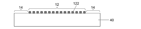
- ⁇ Waviness of temperature sensor film> 4 and 5 are cross-sectional views of the temperature sensor film 110 in the vicinity of the lead portion 11 and the vicinity of the resistance temperature measuring resistance portion 12, respectively. As described above, in the temperature sensor film 110 shown in FIG. 2, the metal thin film 10 remains in the lead portion 11 and the resistance temperature measuring resistance portion 12, and the metal thin film 10 can be removed in the other regions 14. The flexible substrate 40 is exposed.
- FIG. 6 and 7 are cross-sectional views of a temperature sensor film having a remaining portion of the metal thin film 10 in addition to the lead portion and the resistance temperature measuring resistance portion
- FIG. 6 is a cross-sectional view in the vicinity of the lead portion 11
- FIG. 7 is a temperature measuring resistance. It is sectional drawing in the vicinity of part 12.
- the residual piece 15c of the metal thin film exists in the region sandwiched between the lead wiring 11a and the lead wiring 11b, and the lead wiring 11a and the residual piece 15c are the region 16a in which the metal film is removed in a groove shape.
- the lead wiring 11b and the residual piece 15c are separated by a region 16b from which the metal film has been removed in a groove shape.
- a residual portion 15 of the metal thin film is also present on the outside of the lead portion, and the metal thin film in the residual portion is separated from the lead portion by a region 16 in which the metal film is removed in a groove shape.
- the metal thin film removing region 16 exists so as to surround the resistance temperature measuring resistance portion 12, and the metal thin film remains without being removed in the metal thin film remaining region 15 on the outer periphery thereof.
- the regions where the metal thin film is provided on the flexible substrate 40 are provided wirings 11a and 11b, the sensor wiring (longitudinal wiring) 122 of the resistance temperature detector 12), and these are There are regions 15) where the metal thin film remains electrically separated, and regions 14 and 16 where the metal thin film is removed and the flexible substrate 40 is exposed.
- a step is formed along the boundary between the lead wirings 11a and 11b and the flexible substrate exposed regions 14 and 16, and the lead wirings 11a and 11b (and the residual piece 15c) are convex or convex. It becomes a recess and has a wavy shape along a direction orthogonal to the extending direction of the lead wiring.
- a step is generated along the outer circumference of the resistance temperature detector 12, and a swell is generated in which the resistance temperature detector is convex or concave (see Comparative Example 5 in FIG. 8).
- the rate of change in heating dimensions between the region where the metal thin film is provided and the region where the metal thin film is not provided was the cause of the swell. That is, the heating dimensional change rate H 1 in the region where the metal thin film 10 is provided on the flexible substrate 40 and the heating dimensional change rate H 2 in the region where the metal thin film is removed and the flexible substrate 40 is exposed. Is one of the factors that cause waviness, and when the absolute value of the difference between H 1 and H 2
- the heating dimension change rate (%) is defined as 100 ⁇ (LL 0 ) / L 0 using the distance L 0 between two points before heating and the distance L between two points after heating.
- the "heating dimensional change rate” represents the dimensional change rate in a predetermined direction before and after heating when heated at 150 ° C. for 25 minutes, unless otherwise specified.
- the sign of the heating dimension change rate is positive, it indicates expansion, and when it is negative, it indicates contraction. If it is H 2 -H 1> 0 is a region where the metal thin film is provided, it means that the size after heating as compared to a region where the metal thin film has been removed is small (likely to thermal contraction).
- H 2 -H 1> 0 tends to swell the film occurs as recess a region where the metal thin film is provided, the metal thin film is removed regions a convex portion. If it is H 2 -H 1 ⁇ 0 tends to swell the film occurs as the convex portion area where the metal thin film is provided, a region where the metal thin film is removed becomes concave. If it is H 2 -H 1> 0, to heat shrinkage of the metal thin film is larger than the heat shrinkage of the flexible substrate is considered that the thermal shrinkage of the area where the metal thin film is provided is increased.
- the temperature sensor film in which the metal thin film is patterned has wavy waviness so that the metal thin film side of the region where the metal thin film is provided is inside (concave).
- the waviness of the film after patterning the metal thin film is small or no waviness occurs, it is excellent in handleability and contributes to the improvement of the productivity and yield of the temperature sensor element. Further, when the protective film is attached to the surface of the temperature sensor film, problems such as air bubbles entering the bonding interface can be suppressed.
- is preferably 0.10% or less, more preferably 0.07% or less, still more preferably 0.05% or less. Since the smaller the
- the difference in the heating dimensional change rate in any one direction may be within the above range.
- the difference in the rate of change in heating dimension in the patterning direction is within the above range.
- the difference in the rate of change in heating dimensions in all directions is within the above range.
- the residual stress at the film formation interface when the metal thin film 10 is formed on the flexible substrate 40 is reduced, and the flexible substrate 40 and / or the metal is used.
- Examples thereof include a method of reducing the external action that causes a change in the heating dimension of the thin film 10. Also, the larger the thickness of the metal thin film, it tends to H 2 -H 1 increases.
- the flexible substrate 40 includes a resin film base material 50.
- the resin film base material 50 may be transparent or opaque.
- the resin film base material 50 may be made of only a resin film, or may have a hard coat layer (cured resin layer) 6 on the surface of the resin film 5 as shown in FIG.
- the thickness of the resin film base material 50 may be 1 mm or less. From the viewpoint of achieving both strength and flexibility, the thickness of the resin film base material 50 is generally about 2 to 500 ⁇ m, preferably about 20 to 300 ⁇ m.
- An easy-adhesive layer, an antistatic layer, and the like are provided on the surface of the resin film base material 50 (when the hard coat layer 6 is provided, the surface of the resin film 5 and / or the surface of the hard coat layer 6). You may be.
- the surface of the resin film base material 50 may be subjected to treatments such as corona discharge treatment, ultraviolet irradiation treatment, plasma treatment, and sputtering etching treatment for the purpose of improving the adhesion to the base layer 20 and the like.
- the resin material of the resin film 5 examples include polyester such as polyethylene terephthalate, polyimide, polyolefin, cyclic polyolefin such as norbornene, polycarbonate, polyether sulfone, polyarylate and the like. Polyimide or polyester is preferable from the viewpoints of heat resistance, dimensional stability, electrical properties, mechanical properties, chemical resistance properties, and the like.
- the thickness of the resin film 5 is not particularly limited, but is generally about 2 to 500 ⁇ m, preferably about 20 to 300 ⁇ m.
- the hard coat layer 6 By providing the hard coat layer 6 on the surface of the resin film 5, the hardness of the conductive film is improved and the scratch resistance is enhanced.
- the hard coat layer 6 can be formed, for example, by applying a solution containing a curable resin onto the resin film 5.
- the curable resin examples include thermosetting resins, ultraviolet curable resins, and electron beam curable resins.
- the curable resin examples include various resins such as polyester-based, acrylic-based, urethane-based, acrylic-urethane-based, amide-based, silicone-based, silicate-based, epoxy-based, melamine-based, oxetane-based, and acrylic urethane-based.
- acrylic resins, acrylic urethane resins, and epoxy resins are preferable because they have high hardness, can be cured by ultraviolet rays, and have excellent productivity.
- an acrylic resin and an acrylic urethane resin are preferable because they have high adhesion to the chromium oxide thin film contained in the base layer.
- the UV curable resin includes UV curable monomers, oligomers, polymers and the like. Examples of the ultraviolet curable resin preferably used include those having an ultraviolet polymerizable functional group, and among them, those containing an acrylic monomer or oligomer having 2 or more, particularly 3 to 6 of the functional groups as a component.
- the hard coat layer 6 may contain fine particles.
- the fine particles include various metal oxide fine particles such as silica, alumina, titania, zirconia, calcium oxide, tin oxide, indium oxide, cadmium oxide, and antimony oxide, glass fine particles, polymethylmethacrylate, polystyrene, polyurethane, and acrylic-styrene common weight.
- Crosslinked or uncrosslinked organic fine particles, silicone-based fine particles, etc. made of a polymer such as coalesced, benzoguanamine, melamine, or polycarbonate can be used without particular limitation.
- the average particle size (average primary particle size) of the fine particles is preferably about 10 nm to 10 ⁇ m.
- fine particles having an average particle size of about 0.5 ⁇ m to 10 ⁇ m, preferably about 0.8 ⁇ m to 5 ⁇ m, or an average particle size on the order of ⁇ m (hereinafter, may be referred to as “microparticles”) in the hard coat layer.
- microparticles an average particle size on the order of ⁇ m (hereinafter, may be referred to as “microparticles”) in the hard coat layer.
- Submicron or ⁇ m diameter protrusions are formed on the surface of the hard coat layer 6 (the surface of the resin film base material 50) and the surface of the thin film provided on the surface, and the slipperiness and blocking resistance of the conductive film are formed. , And tends to improve scratch resistance.
- the hard coat layer contains fine particles (nanoparticles) having an average particle size of about 10 nm to 100 nm, preferably about 20 nm to 80 nm, so that the surface of the hard coat layer 6 (the surface of the resin film base material 50) is fine. The unevenness is formed, and the adhesion between the hard coat layer 6 and the base layer 20 and the metal thin film 10 tends to be improved.
- the solution for forming the hard coat layer contains an ultraviolet polymerization initiator.
- the solution may contain additives such as a leveling agent, a thixotropy agent, and an antistatic agent.
- the thickness of the hard coat layer 6 is not particularly limited, but in order to achieve high hardness, 0.5 ⁇ m or more is preferable, 0.8 ⁇ m or more is more preferable, and 1 ⁇ m or more is further preferable. Considering the ease of formation by coating, the thickness of the hard coat layer is preferably 15 ⁇ m or less, more preferably 10 ⁇ m or less.
- the flexible substrate 40 may include a base layer 20 on the resin film base material 50.
- the base layer 20 may be a single layer, or may be a laminated structure of two or more thin films 21 and 22 as shown in FIG.
- the base layer 20 may be an organic layer or an inorganic layer, or may be a laminate of an organic layer and an inorganic layer, but at least one layer is preferably an inorganic thin film, and in particular, a thin film 22 provided directly under the metal thin film 10. Is preferably an inorganic thin film.
- the inorganic thin film as the base layer 20
- the mixing of organic gas from the resin film base material 50 into the metal thin film 10 is suppressed, and the temperature coefficient of resistance (TCR) of the metal thin film 10 is suppressed.
- TCR temperature coefficient of resistance
- tends to decrease.
- One of the estimation factors that reduces the difference in the rate of change in heating dimensions by providing the base layer is the stress relaxation effect of the base layer.
- the formation of an amorphous base layer on the resin film base material is expected to have the effect of alleviating the stress caused by the mismatch of the lattice spacing of the metal thin film.
- the fact that the base layer on the resin film base material acts as a barrier layer is also considered to be one of the factors that reduce the difference in the rate of change in heating dimensions.
- the base layer By acting as a barrier layer, the base layer suppresses the mixing of impurities such as water and organic substances from the resin film base material into the metal thin film. Therefore, a metal thin film having few lattice defects is likely to be formed, and the dimensional change of the metal thin film due to the rearrangement of atoms during heating is unlikely to occur. Therefore, it is considered that the difference in the heating dimensional change rate depending on the presence or absence of the metal thin film is small.
- the base layer 20 may be conductive or insulating.
- the thin film 22 arranged directly under the metal thin film 10 is a conductive inorganic material (inorganic conductor)
- the thin film 21 (or the entire base layer 20) can be patterned together with the metal thin film 10 when the temperature sensor film is produced. Good.
- the thin film 21 is an insulating inorganic material (inorganic dielectric)
- the thin film 21 may or may not be patterned.
- Inorganic materials include Si, Ge, Sn, Pb, Al, Ga, In, Tl, As, Sb, Bi, Se, Te, Mg, Ca, Sr, Ba, Sc, Y, Ti, Zr, Hf, V. , Nb, Ta, Cr, Mo, W, Mn, Tc, Re, Fe, Ru, Os, Ni, Co, Rh, Ir, Pd, Pt, Cu, Ag, Au, Zn, Cd and other metal elements or metalloids.
- Examples include metal elements and alloys, nitrides, oxides, carbides, nitrogen oxides and the like thereof.
- the underlayer As a material for the underlayer, it has excellent adhesion to both the organic material constituting the hard coat layer 6 and the metal material such as nickel constituting the metal thin film 10, and has a high effect of suppressing impurities from being mixed into the metal thin film. Silicon-based materials or chromium oxide are preferred.
- silicon-based materials include silicon and silicon compounds such as silicon oxide, silicon nitride, silicon oxynitride, and silicon carbide. Of these, silicon or silicon oxide is preferable because it has excellent adhesion to the hard coat layer and the metal thin film and has an excellent effect of improving bending resistance. From the viewpoint of ensuring insulation between the wirings when the metal thin film 10 is patterned, the layer 22 immediately below the metal thin film 10 is preferably an inorganic dielectric thin film such as silicon oxide.
- Silicon oxide may have a stoichiometric composition (SiO 2 ) or a non-stoichiometric composition (SiO x ; x ⁇ 2).
- the silicon oxide (SiO x ) having a non-stoichiometric composition preferably has 1.2 ⁇ x ⁇ 2.
- the silicon oxide thin film 22 may be formed on the silicon thin film 21. Further, a silicon oxide thin film may be formed on the inorganic thin film 21 made of various metals, conductive oxides, ceramics and the like.
- the thickness of the base layer 20 and the thickness of the thin film constituting the base layer 20 are not particularly limited. From the viewpoint of suppressing the waviness of the film after patterning the metal thin film by the base effect on the metal thin film 10, the effect of reducing plasma damage to the resin film base material at the time of forming the metal thin film and the effect of blocking outgas from the resin film base material can be obtained. From the viewpoint of increasing, the thickness of the base layer 20 is preferably 1 nm or more, more preferably 3 nm or more, still more preferably 5 nm or more. From the viewpoint of improving productivity and reducing material cost, the thickness of the base layer is preferably 200 nm or less, more preferably 100 nm or less, still more preferably 50 nm or less.
- the method of forming the base layer 20 is not particularly limited, and either dry coating or wet coating can be adopted depending on the material.
- the metal thin film 10 is formed by the sputtering method, it is preferable that the base layer 20 is also formed by the sputtering method from the viewpoint of productivity.
- the target When forming the base layer by the sputtering method, the target may be selected according to the material of the base layer. For example, when forming a silicon thin film, a silicon target is used. A silicon oxide target may be used for forming the silicon oxide thin film, or silicon oxide may be formed by reactive sputtering using the silicon target. In the reactive sputtering, it is preferable to adjust the amount of oxygen so as to be an intermediate transition region between the metal region and the oxide region.
- the metal thin film 10 provided on the flexible substrate 40 plays a central role in temperature measurement in the temperature sensor. As described above, the temperature sensor film is formed by patterning the metal thin film 10.
- metal materials constituting the metal thin film 10 include copper, silver, aluminum, gold, rhodium, tungsten, molybdenum, zinc, tin, cobalt, indium, nickel, iron, platinum, palladium, tin, antimony, bismuth, and magnesium. , And alloys of these.
- nickel, copper, or an alloy containing these as a main component is preferable because of its low resistance, high TCR, and inexpensive material, and nickel or nickel is mainly used.
- a nickel alloy as a component is preferable.
- the thickness of the metal thin film 10 is not particularly limited, but is preferably 20 nm or more from the viewpoint of reducing resistance (particularly, from the viewpoint of reducing the resistance of the lead portion), and preferably 500 nm or less from the viewpoint of improving patterning accuracy and the like.
- the thickness of the metal thin film 10 is small, tends to H 2 -H 1 for heat shrinkage of the metal thin film is small is reduced, H 2 -H 1 ⁇ 0, and the after patterning the metal thin film, a metal thin film There is a tendency for waviness to occur in which the provided area is convex.
- the thickness of the metal thin film 10 is preferably 60 to 200 nm, more preferably 70 to 180 nm.
- the specific resistance at a temperature of 25 ° C. is preferably 1.6 ⁇ 10 -5 ⁇ ⁇ cm or less, more preferably 1.5 ⁇ 10 -5 ⁇ ⁇ cm or less. ..
- the TCR of the metal thin film 10 is preferably 3000 ppm / ° C. or higher, more preferably 3400 ppm / ° C. or higher, further preferably 3600 ppm / ° C. or higher, and particularly preferably 3800 ppm / ° C. or higher.
- TCR is the rate of change of resistance with respect to temperature rise. Metals such as nickel and copper have the property (positive property) that the resistance linearly increases as the temperature rises.
- the larger the TCR the larger the change in resistance to temperature changes, and the higher the temperature measurement accuracy in the temperature sensor film. Therefore, the larger the TCR of the metal thin film is, the more preferable it is, but it is difficult to make the TCR larger than that of the bulk metal, and the TCR of the metal thin film is generally 6000 ppm / ° C. or less.
- the method for forming the metal thin film is not particularly limited, and for example, a deposition method such as a sputtering method, a vacuum vapor deposition method, an electron beam vapor deposition method, a chemical vapor deposition method (CVD), a chemical solution deposition method (CBD), or a plating method can be used. Can be adopted. Among these, the sputtering method is preferable because a thin film having excellent film thickness uniformity can be formed. The productivity of the conductive film is enhanced by forming a film while continuously moving a long resin film base material in the longitudinal direction using a roll-to-roll sputtering apparatus.
- the inside of the sputtering apparatus is exhausted before the start of sputtering film formation, and the organic gas generated from the film substrate is exhausted. It is preferable to create an atmosphere in which impurities such as the above are removed. By removing the gas in the apparatus and the film base material in advance, the amount of water, organic gas, or the like mixed in the metal thin film 10 can be reduced.
- the degree of vacuum (reached vacuum degree) in the sputtering apparatus before the start of sputtering film formation is, for example, 1 ⁇ 10 -1 Pa or less, preferably 5 ⁇ 10 -2 Pa or less, and more preferably 1 ⁇ 10 -2 Pa or less. preferable.
- a metal target is used for sputter film formation of a metal thin film, and film formation is performed while introducing an inert gas such as argon.
- an inert gas such as argon.
- a metal Ni target is used when forming a nickel thin film as the metal thin film 10.
- Sputter film formation conditions are not particularly limited.
- the base layer 20 on the resin film base material 50 and forming the metal thin film 10 on the base layer 20 plasma damage to the resin film base material 50 at the time of forming the metal thin film 10 can be suppressed.
- the base layer 20 it is possible to block water, organic gas, etc. generated from the resin film base material 50, and suppress mixing of water, organic gas, etc. into the metal thin film 10.
- the substrate temperature in the sputter film formation of the metal thin film is preferably 200 ° C. or lower, more preferably 180 ° C. or lower, and even more preferably 170 ° C. or lower.
- the substrate temperature is preferably ⁇ 30 ° C. or higher.
- the discharge power density is preferably 1 ⁇ 15W / cm 2, more preferably 1.5 ⁇ 10W / cm 2.
- the temperature sensor film can be produced by patterning the metal thin film 10 of the conductive film.
- the patterning method of the metal thin film is not particularly limited. Since patterning is easy and the accuracy is high, it is preferable to perform patterning by a photolithography method or laser processing. In photolithography, an etching resist corresponding to the shapes of the lead portion and the temperature measuring resistance portion is formed on the surface of the metal thin film, and the metal thin film in the region where the etching resist is not formed is removed by wet etching and then etched. Peel off the resist.
- the patterning of the metal thin film can also be performed by dry etching such as laser processing.
- the conductive film of the present invention As described above, the conductive film of the present invention, the dimensional change rate upon heating H 1 of the conductive film before patterning the metal thin film, a conductive film of the difference between the dimensional change rate upon heating of H 2 film has been removed a metal thin film
- the absolute value is small. Therefore, the temperature sensor film after patterning the metal thin film, the dimensional change rate upon heating h 1 of the region the metal thin film is provided, the difference in heat dimension change rate h 2 regions metal thin film is not provided h 2
- the absolute value of -h 1 also becomes smaller. Therefore, even if the etchant is heated at the time of drying after washing with water, the generation of swell due to the difference in the heating dimensional change is suppressed.
- is preferably 0.10% or less, more preferably 0.07% or less, still more preferably 0.05% or less. Since the smaller the
- a plurality of lead portions and resistance temperature measuring resistance portions can be formed on the substrate surface.
- a temperature sensor element can be obtained by connecting the connector 19 to the end of the lead portion 11 of the temperature sensor film.
- lead portions are connected to a plurality of resistance temperature detectors, and the plurality of lead portions may be connected to one connector 19. Therefore, it is possible to easily form a temperature sensor element capable of measuring the temperature at a plurality of locations in the plane.
- connection method between the lead portion of the temperature sensor film and the external circuit is not limited to the form via the connector.
- a controller for applying a voltage to the lead portion to measure the resistance may be provided on the temperature sensor film.
- the lead portion and the lead wiring from the external circuit may be connected by soldering or the like without using a connector.
- the temperature sensor film has a simple structure in which a metal thin film is provided on a flexible substrate, and is excellent in productivity.
- the handleability is excellent.
- Example 1 ⁇ Preparation of film substrate with hard coat layer> Contains crosslinked polymethyl methacrylate particles having an average particle diameter of 1.5 ⁇ m (“Techpolymer SSX-101” manufactured by Sekisui Plastics Co., Ltd.) and an ultraviolet curable urethane acrylate resin (“Aika Aitron Z844-22HL” manufactured by Aika Kogyo Co., Ltd.). A coating composition using methyl isobutyl ketone as a solvent was prepared. The amount of particles in the composition was 0.2 parts by weight with respect to 100 parts by weight of the solid content of the binder resin.
- PET polyethylene terephthalate
- ⁇ Formation of metal thin film> The roll of the film base material with the hard coat layer described above is set in the roll-to-roll sputtering apparatus, and after exhausting the inside of the sputtering apparatus until the ultimate vacuum reaches 5 ⁇ 10 -3 Pa, argon is introduced as a sputtering gas. Then, a nickel thin film having a thickness of 70 nm was formed on the hard coat layer forming surface by DC sputtering under the conditions of a substrate temperature of 40 ° C., a pressure of 0.25 Pa, and a power density of 5.0 W / cm 2.
- Example 2 A conductive film having a nickel thin film on the hard coat layer was produced in the same manner as in Example 1 except that the substrate temperature at the time of forming the nickel thin film was changed to 80 ° C.
- Example 3 A film substrate with a hard coat layer was prepared in the same manner as in Example 1, set in a roll-to-roll sputtering apparatus, and the inside of the sputtering apparatus was exhausted until the ultimate vacuum degree became 5 ⁇ 10 -3 Pa, and then the substrate temperature.
- a silicon thin film having a thickness of 5 nm, a silicon oxide thin film having a thickness of 10 nm, and a nickel thin film having a thickness of 70 nm were sequentially formed on the hard coat layer forming surface by DC sputtering, and then formed on the hard coat layer underneath.
- a conductive film provided with a nickel thin film was produced via a silicon thin film as a formation layer and a silicon oxide thin film.
- a B-doped Si target was used to form the Si layer and the SiO 2 layer.
- Argon was introduced as a sputtering gas into the Si layer, and a film was formed under the conditions of a pressure of 0.3 Pa and a power density of 1.0 W / cm 2.
- the film was formed under the conditions.
- the film forming conditions for the nickel thin film were the same as those in Example 1 except that the substrate temperature was changed to 150 ° C.
- Example 4 A nickel thin film was formed on the hard coat layer via a silicon thin film as a base layer and a silicon oxide thin film in the same manner as in Example 3 except that the substrate temperature was changed to 80 ° C. and the film thickness of the nickel thin film was changed to 160 nm. A conductive film to be provided was produced.
- Example 5 Conductivity in which a nickel thin film is provided on the hard coat layer via a chromium thin film as an underlayer and a silicon oxide thin film in the same manner as in Example 3 except that a metallic chromium thin film having a thickness of 5 nm is formed instead of the silicon thin film.
- a film was made.
- a metallic chromium target was used to form the chromium thin film, argon was introduced as a sputtering gas, and the film was formed under the conditions of a pressure of 0.25 Pa and a power density of 0.74 W / cm 2.
- ITO indium tin oxide
- Example 1 A conductive film having a nickel thin film on the hard coat layer via a silicon thin film as a base layer and a silicon oxide thin film was produced in the same manner as in Example 4 except that the thickness of the nickel thin film was changed to 50 nm.
- Example 2 A conductive film having the nickel thin film on the hard coat layer was produced in the same manner as in Example 2 except that the thickness of the nickel thin film was changed to 220 nm.
- Example 3 A conductive film having the nickel thin film on the hard coat layer was produced in the same manner as in Example 2 except that the thickness of the nickel thin film was changed to 260 nm.
- a 100 mm ⁇ 100 mm square test piece was cut out from the conductive film and immersed in hydrochloric acid to remove the nickel thin film by etching. Thereafter, in the same manner as above was measured dimensional change rate upon heating of H 2 after 155 ° C. 25 minutes heating the MD and TD directions.
- a 70 mm ⁇ 70 mm square test piece was cut out from the conductive film, and a polyimide tape having a width of 2 mm was attached to the surface of the nickel thin film in a striped manner at intervals of 2 mm.
- This test piece was immersed in hydrochloric acid to remove the nickel thin film in the region where the polyimide tape was not attached by etching, washed with water by immersion in pure water, and then the polyimide tape was slowly peeled off. It was allowed to stand in a heating oven at 155 ° C. for 25 minutes and allowed to cool to room temperature.
- the coherence scanning interferometer Zygo NewView 7300 was used to measure the three-dimensional surface shape under the following conditions, and the maximum value of the height difference between the peaks and valleys adjacent to the patterning direction was taken as the amount of undulation. If the part where the nickel thin film is provided is a recess (valley), the sign of the swell amount is positive, and if the part where the nickel thin film is provided is a recess (peak), the sign of the swell amount is positive. Was negative.
- composition of the conductive films of Examples and Comparative Examples (the composition of the base layer, the thickness of the nickel thin film and the substrate temperature), the rate of change in heating dimensions in the MD direction, the amount of waviness when the MD direction is the patterning direction, and the heating in the TD direction.
- Table 1 shows the dimensional change rate and the amount of waviness when the TD direction is the patterning direction.
- FIG. 8 shows an observation image of a sample obtained by laser-patterning the conductive films of Example 4 and Comparative Example 2 under a fluorescent lamp.
- the heating shrinkage in the MD direction tended to be larger than that in the TD direction. This is because the production of the resin film and the formation of the hard coat layer, the base layer and the metal thin film on the resin film are all carried out by the roll-to-roll process, and the film is stretched in the MD direction due to the tension during transportation. It is considered that the film tends to shrink in the MD direction when heated without applying tension.
- Example 5 the reflected image of the fluorescent lamp is linear, whereas in Comparative Example 2, the reflected image of the fluorescent lamp is distorted around the patterning region, causing swelling. .. From these results, not only when the metal thin film is patterned by wet etching, but also when the metal thin film is patterned by a dry process such as laser processing , the smaller
Landscapes
- Chemical & Material Sciences (AREA)
- Physics & Mathematics (AREA)
- General Physics & Mathematics (AREA)
- Chemical Kinetics & Catalysis (AREA)
- Engineering & Computer Science (AREA)
- Materials Engineering (AREA)
- Mechanical Engineering (AREA)
- Metallurgy (AREA)
- Organic Chemistry (AREA)
- Thermistors And Varistors (AREA)
- Surface Heating Bodies (AREA)
Abstract
Description
図1は、温度センサフィルムの形成に用いられる導電フィルムの積層構成例を示す断面図である。導電フィルム101は、可撓性基板40の一方の主面上に金属薄膜10を備える。可撓性基板40は樹脂フィルム基材50を含み、樹脂フィルム基材50の金属薄膜形成面側に下地層20を備えていてもよい。樹脂フィルム基材50は、樹脂フィルム5の表面にハードコート層6を備えていてもよい。
図4および図5は、それぞれ、温度センサフィルム110のリード部11近傍および測温抵抗部12近傍の断面図である。上記で説明したように、図2に示す温度センサフィルム110では、リード部11および測温抵抗部12には金属薄膜10が残存しており、その他の領域14では金属薄膜10が除去されて可撓性基板40が露出している。
以下、図1を参照しながら、温度センサフィルムの形成に用いられる導電フィルム101の構成および製造方法について説明する。
可撓性基板40は、樹脂フィルム基材50を含む。樹脂フィルム基材50は、透明でも不透明でもよい。樹脂フィルム基材50は、樹脂フィルムのみからなるものでもよく、図1に示すように、樹脂フィルム5の表面にハードコート層(硬化樹脂層)6を備えるものでもよい。樹脂フィルム基材50の厚みは1mm以下であればよい。強度と可撓性を両立する観点から、樹脂フィルム基材50の厚みは、一般に2~500μm程度であり、20~300μm程度が好ましい。
樹脂フィルム5の樹脂材料としては、ポリエチレンテレフタレート等のポリエステル、ポリイミド、ポリオレフィン、ノルボルネン系等の環状ポリオレフィン、ポリカーボネート、ポリエーテルスルフォン、ポリアリレート等が挙げられる。耐熱性、寸法安定性、電気的特性、機械的特性、耐薬品特性等の観点から、ポリイミドまたはポリエステルが好ましい。樹脂フィルム5の厚みは特に限定されないが、一般には、2~500μm程度であり、20~300μm程度が好ましい。
樹脂フィルム5の表面にハードコート層6が設けられることにより、導電フィルムの硬度が向上し、耐擦傷性が高められる。ハードコート層6は、例えば、樹脂フィルム5上に、硬化性樹脂を含有する溶液を塗布することにより形成できる。
可撓性基板40は、樹脂フィルム基材50上に下地層20を備えていてもよい。下地層20は単層でもよく、図1に示すように2層以上の薄膜21,22の積層構成でもよい。下地層20は有機層でも無機層でもよく、有機層と無機層とを積層したものでもよいが、少なくとも1層は無機薄膜であることが好ましく、特に、金属薄膜10の直下に設けられる薄膜22が無機薄膜であることが好ましい。下地層20として無機薄膜が設けられることにより、金属薄膜10を形成する際に、樹脂フィルム基材50からの金属薄膜10への有機ガスの混入が抑制され、金属薄膜10の抵抗温度係数(TCR)が大きくなる傾向があり、温度センサフィルムにおける温度測定精度が向上する。
可撓性基板40上に設けられる金属薄膜10は、温度センサにおける温度測定の中心的な役割を果たす。前述のように、金属薄膜10をパターニングすることにより、温度センサフィルムが形成される。
TCR={(R1-R0)/R0}/(T1-T0)
上記のように、導電フィルムの金属薄膜10をパターニングすることにより、温度センサフィルムを作製できる。金属薄膜のパターニング方法は特に限定されない。パターニングが容易であり、精度が高いことからフォトリソグラフィー法またはレーザ加工によりパターニングを行うことが好ましい。フォトリソグラフィーでは、金属薄膜の表面に、上記のリード部および測温抵抗部の形状に対応するエッチングレジストを形成し、エッチングレジストが形成されていない領域の金属薄膜をウェットエッチングにより除去した後、エッチングレジストを剥離する。金属薄膜のパターニングは、レーザ加工等のドライエッチングにより実施することもできる。
<ハードコート層付きフィルム基材の作製>
平均粒子径1.5μmの架橋ポリメタクリル酸メチル粒子(積水化成品工業製「テクポリマー SSX-101」)と紫外線硬化型ウレタンアクリレート樹脂(アイカ工業製「アイカアイトロン Z844-22HL」とを含み,メチルイソブチルケトンを溶媒とするコーティング組成物を調製した。組成物中の粒子の量は、バインダー樹脂の固形分100重量部に対して,0.2重量部であった.この組成物を、厚み150μmのポリエチレンテレフタレート(PET)フィルム(東レ製「ルミラー 149UNS」)の一方の面に塗布し、100℃で1分間乾燥した。その後,紫外線照射により硬化処理を行い,厚み0.8μmのハードコート層を形成した。
ロールトゥーロールスパッタ装置内に、上記のハードコート層付きフィルム基材のロールをセットし、スパッタ装置内を到達真空度が5×10⁻³Paとなるまで排気した後、スパッタガスとしてアルゴンを導入し、基板温度40℃、圧力0.25Pa、パワー密度5.0W/cm2の条件で、ハードコート層形成面上にDCスパッタにより厚み70nmのニッケル薄膜を成膜した。
ニッケル薄膜成膜時の基板温度を80℃に変更したこと以外は、実施例1と同様にして、ハードコート層上にニッケル薄膜を備える導電フィルムを作製した。
実施例1と同様にハードコート層付きフィルム基材を作成し、ロールトゥーロールスパッタ装置内にセットし、スパッタ装置内を到達真空度が5×10⁻³Paとなるまで排気した後、基板温度150℃にて、ハードコート層形成面上に、厚み5nmのシリコン薄膜、厚み10nmの酸化シリコン薄膜、および厚み70nmのニッケル薄膜を、順に、DCスパッタにより成膜し、ハードコート層上に、下地層としてのシリコン薄膜および酸化シリコン薄膜を介してニッケル薄膜を備える導電フィルムを作製した。Si層およびSiO2層の形成には、BドープSiターゲットを用いた。Si層は、スパッタガスとしてアルゴンを導入し、圧力0.3Pa、パワー密度1.0W/cm2の条件で成膜した。SiO2層は、スパッタガスとしてのアルゴンに加えて反応性ガスとして酸素を導入し(O2/Ar=0.12/1.0)、圧力0.3Pa、パワー密度1.8W/cm2の条件で成膜した。ニッケル薄膜の成膜条件は、基板温度を150℃に変更したこと以外は、実施例1と同様とした。
基板温度を80℃、ニッケル薄膜の膜厚を160nmに変更したこと以外は、実施例3と同様にして、ハードコート層上に、下地層としてのシリコン薄膜および酸化シリコン薄膜を介してニッケル薄膜を備える導電フィルムを作製した。
シリコン薄膜に代えて厚み5nmの金属クロム薄膜を形成したこと以外は、実施例3と同様にして、ハードコート層上に、下地層としてのクロム薄膜および酸化シリコン薄膜を介してニッケル薄膜を備える導電フィルムを作製した。クロム薄膜の形成には金属クロムターゲットを用い、スパッタガスとしてアルゴンを導入し、圧力0.25Pa、パワー密度0.74W/cm2の条件で成膜した。
シリコン薄膜に代えて厚み5nmの酸化インジウム錫(ITO)薄膜を形成したこと以外は、実施例3と同様にして、ハードコート層上に、下地層としてのITO薄膜および酸化シリコン薄膜を介してニッケル薄膜を備える導電フィルムを作製した。ITO薄膜の形成には酸化インジウム錫の焼結ターゲットを用い、スパッタガスとしてアルゴンに加えて酸素を導入し(O2/Ar=0.12/1.0)、圧力0.19Pa、パワー密度1.82W/cm2の条件で成膜した。
シリコン薄膜に代えて厚み10nmのアルミニウムドープ酸化亜鉛(AZO)薄膜を形成したこと以外は、実施例3と同様にして、ハードコート層上に、下地層としてのAZO薄膜および酸化シリコン薄膜を介してニッケル薄膜を備える導電フィルムを作製した。AZO薄膜の形成には酸化アルミニウムドープ酸化亜鉛の焼結ターゲットを用い、スパッタガスとしてアルゴンに加えて酸素を導入し(O2/Ar=0.12/1.0)、圧力0.19Pa、パワー密度0.75W/cm2の条件で成膜した。
ニッケル薄膜の厚みを50nmに変更したこと以外は、実施例4と同様にして、ハードコート層上に、下地層としてのシリコン薄膜および酸化シリコン薄膜を介してニッケル薄膜を備える導電フィルムを作製した。
ニッケル薄膜の厚みを220nmに変更したこと以外は、実施例2と同様にして、ハードコート層上にニッケル薄膜を備える導電フィルムを作製した。
ニッケル薄膜の厚みを260nmに変更したこと以外は、実施例2と同様にして、ハードコート層上にニッケル薄膜を備える導電フィルムを作製した。
<加熱寸法変化率>
導電フィルムから100mm×100mmの正方形の試験片を切り出し、MD方向(スパッタ成膜時の搬送方向)およびTD方向(MD方向と直交する方向)に、80mm間隔で4点の標点(傷)を形成し、標点間の距離L0を表面座標測定機(TOPCON製「CP600S」)により測定した。155℃の加熱オーブン中で25分間静置し、室温まで放冷した後、標点間の距離Lを測定した。MDおよびTDのそれぞれについて、2か所の加熱寸法変化率の平均を、導電フィルムの加熱寸法変化率H1とした。
導電フィルムから70mm×70mmの正方形の試験片を切り出し、ニッケル薄膜の表面に幅2mmのポリイミドテープを2mm間隔でストライプ状に貼り合わせた。この試験片を塩酸に浸漬して、ポリイミドテープが貼り合わせられていない領域のニッケル薄膜をエッチング除去し、純水への浸漬により水洗した後、ポリイミドテープをゆっくりと剥離した。155℃の加熱オーブン中で25分間静置し、室温まで放冷した。MD方向をパターニング方向とした場合(TD方向に延在するようにポリイミドテープを貼り合わせた場合)およびTD方向をパターニング方向とした場合(MD方向に延在するようにポリイミドテープを貼り合わせた場合)のそれぞれについて、コヒーレンス走査型干渉計(Zygo NewView 7300)により、下記の条件で三次元表面形状を測定し、パターニング方向に隣接する山と谷の高低差の最大値をうねり量とした。ニッケル薄膜が設けられている部分が凹部(谷)となっている場合はうねり量の符号を正とし、ニッケル薄膜が設けられている部分が凹部(山)となっている場合はうねり量の符号を負とした。
(測定条件)
対物レンズ:2.5倍、ズームレンズ1倍
測定視野:10mm×5mm
Removed:Cylinder
Filter: OFF
Filter Type: AVERAGE
Remove spikes: OFF
Spike Height (xRMS): 2.50
実施例4および比較例2の導電フィルムを試料として、レーザーパターニングにより、導電フィルムのニッケル薄膜を線幅30μmのストライプ形状(L/S=30μm/30μm)にパターニングし、蛍光灯下にて目視観察し、ニッケル薄膜表面での反射像の歪の有無を確認した。
実施例および比較例の導電フィルムの構成(下地層の構成、ニッケル薄膜の厚みおよび基板温度)、MD方向の加熱寸法変化率およびMD方向をパターニング方向とした場合のうねり量、ならびにTD方向の加熱寸法変化率およびTD方向をパターニング方向とした場合のうねり量を、表1に示す。また、実施例4および比較例2の導電フィルムをレーザーパターニングした試料の蛍光灯下での観察像を図8に示す。

50 樹脂フィルム基材
5 樹脂フィルム
6 ハードコート層
20 下地層
10 金属薄膜(ニッケル薄膜)
11 リード部
12 測温抵抗部
122,123 センサ配線
14 金属薄膜除去領域
15 金属薄膜残存領域
19 コネクタ
101 導電フィルム
110 温度センサフィルム
Claims (10)
- 樹脂フィルムを含む可撓性基板の第一主面上に金属薄膜を有する導電フィルムであって、
前記可撓性基板の厚みが1mm以下であり、
導電フィルムの150℃25分加熱後の寸法変化率H1と、導電フィルムから前記金属薄膜を除去したフィルムの150℃25分加熱後の寸法変化率H2との差の絶対値|H2-H1|が0.10%以下である、温度センサ用導電フィルム。 - 前記可撓性基板は、前記樹脂フィルムの第一主面上にハードコート層を備える、請求項1に記載の温度センサ用導電フィルム。
- 前記可撓性基板は、無機薄膜からなる下地層を備え、前記下地層が前記金属薄膜と接している、請求項1または2に記載の温度センサ用導電フィルム。
- 前記下地層は、少なくとも1層のシリコン系薄膜を含む、請求項3に記載の温度センサ用導電フィルム。
- 前記金属薄膜が前記シリコン系薄膜に接している、請求項4に記載の温度センサ用導電フィルム。
- 前記金属薄膜の厚みが、60~200nmである、請求項1~5のいずれか1項に記載の温度センサ用導電フィルム。
- 前記金属薄膜がニッケルまたはニッケル合金からなる、請求項1~6のいずれか1項に記載の温度センサ用導電フィルム。
- 請求項1~7のいずれか1項に記載の導電フィルムを製造する方法であって、
前記金属薄膜をスパッタ法により成膜する、導電フィルムの製造方法。 - 可撓性基板の第一主面上にパターニングされた金属薄膜を備え、
前記金属薄膜が、細線にパターニングされ温度測定に用いられる測温抵抗部と、前記測温抵抗部に接続され、前記測温抵抗部よりも大きな線幅にパターニングされたリード部とにパターニングされており、
前記金属薄膜が設けられている領域の150℃25分加熱後の寸法変化率h1と、前記金属薄膜が設けられていない領域の150℃25分加熱後の寸法変化率h2との差の絶対値|h2-h1|が0.10%以下である、温度センサフィルム。 - 可撓性基板の第一主面上にパターニングされた金属薄膜を備え、前記金属薄膜が、細線にパターニングされ温度測定に用いられる測温抵抗部と、前記測温抵抗部に接続され、前記測温抵抗部よりも大きな線幅にパターニングされたリード部とにパターニングされている温度センサフィルムの製造方法であって、
請求項1~7のいずれか1項に記載の導電フィルムの金属薄膜を、面内の一部の領域で除去することによりパターニングして、前記測温抵抗部および前記リード部を形成する、温度センサフィルムの製造方法。
Priority Applications (4)
| Application Number | Priority Date | Filing Date | Title |
|---|---|---|---|
| CN202080068969.6A CN114556064A (zh) | 2019-10-01 | 2020-09-16 | 导电膜及其制造方法、以及温度传感器膜及其制造方法 |
| KR1020227014208A KR102954678B1 (ko) | 2019-10-01 | 2020-09-16 | 도전 필름 및 그 제조 방법, 그리고 온도 센서 필름 및 그 제조 방법 |
| US17/765,070 US12135247B2 (en) | 2019-10-01 | 2020-09-16 | Electroconductive film, method for manufacturing same, temperature sensor film, and method for manufacturing same |
| EP20870680.4A EP4040126B1 (en) | 2019-10-01 | 2020-09-16 | Electroconductive film, method for manufacturing same, temperature sensor film, and method for manufacturing same |
Applications Claiming Priority (2)
| Application Number | Priority Date | Filing Date | Title |
|---|---|---|---|
| JP2019181491A JP2021056161A (ja) | 2019-10-01 | 2019-10-01 | 導電フィルムおよびその製造方法、ならびに温度センサフィルムおよびその製造方法 |
| JP2019-181491 | 2019-10-01 |
Publications (1)
| Publication Number | Publication Date |
|---|---|
| WO2021065504A1 true WO2021065504A1 (ja) | 2021-04-08 |
Family
ID=75272513
Family Applications (1)
| Application Number | Title | Priority Date | Filing Date |
|---|---|---|---|
| PCT/JP2020/035027 Ceased WO2021065504A1 (ja) | 2019-10-01 | 2020-09-16 | 導電フィルムおよびその製造方法、ならびに温度センサフィルムおよびその製造方法 |
Country Status (6)
| Country | Link |
|---|---|
| US (1) | US12135247B2 (ja) |
| EP (1) | EP4040126B1 (ja) |
| JP (1) | JP2021056161A (ja) |
| CN (1) | CN114556064A (ja) |
| TW (1) | TWI862690B (ja) |
| WO (1) | WO2021065504A1 (ja) |
Families Citing this family (2)
| Publication number | Priority date | Publication date | Assignee | Title |
|---|---|---|---|---|
| JP2024040688A (ja) * | 2022-09-13 | 2024-03-26 | グンゼ株式会社 | 導電性フィルム |
| CN117871027B (zh) * | 2024-03-11 | 2024-05-07 | 中国航空工业集团公司沈阳空气动力研究所 | 一种柱状热流传感器及其阵列化制备方法 |
Citations (6)
| Publication number | Priority date | Publication date | Assignee | Title |
|---|---|---|---|---|
| JP2005091045A (ja) | 2003-09-12 | 2005-04-07 | Yamari Sangyo Kk | 薄膜抵抗測温シート |
| JP2007232669A (ja) * | 2006-03-03 | 2007-09-13 | Tokyo Univ Of Agriculture & Technology | 温度センサおよびその製造方法 |
| JP2007232598A (ja) * | 2006-03-01 | 2007-09-13 | Ngk Spark Plug Co Ltd | 温度センサ |
| US20080043811A1 (en) * | 2006-08-18 | 2008-02-21 | U.S.A. As Represented By The Administrator Of The National Aeronautics And Space Administration | Flexible Thin Metal Film Thermal Sensing System |
| JP2012182258A (ja) * | 2011-02-28 | 2012-09-20 | Mitsubishi Materials Corp | 温度センサ付き非接触給電装置 |
| JP2013045633A (ja) * | 2011-08-24 | 2013-03-04 | Nitto Denko Corp | 透明導電性フィルムの製造方法 |
Family Cites Families (11)
| Publication number | Priority date | Publication date | Assignee | Title |
|---|---|---|---|---|
| WO1992003833A2 (en) * | 1990-08-15 | 1992-03-05 | Advanced Temperature Devices, Inc. | Thin-film resistance temperature device |
| JPH11354302A (ja) * | 1998-06-09 | 1999-12-24 | Mitsui Mining & Smelting Co Ltd | 薄膜抵抗素子 |
| JP4667471B2 (ja) * | 2007-01-18 | 2011-04-13 | 日東電工株式会社 | 透明導電性フィルム、その製造方法及びそれを備えたタッチパネル |
| JP5928829B2 (ja) | 2013-01-31 | 2016-06-01 | 三菱マテリアル株式会社 | 温度センサ |
| US10343385B2 (en) | 2013-07-18 | 2019-07-09 | Boston Scientific Scimed, Inc. | Bodily implant |
| US9236067B2 (en) | 2013-08-01 | 2016-01-12 | Stmicroelectronics Asia Pacific Pte Ltd | Method and apparatus for speed control of voice coil motor retract operation dependent upon available power |
| US10006717B2 (en) | 2014-03-07 | 2018-06-26 | Taiwan Semiconductor Manufacturing Company, Ltd. | Adaptive baking system and method of using the same |
| US9828825B2 (en) | 2015-04-10 | 2017-11-28 | Baker Hughes, A Ge Company, Llc | Positive locating feature of optiport |
| CN109416406B (zh) | 2016-07-05 | 2023-06-20 | 深圳帧观德芯科技有限公司 | 具有不同热膨胀系数的接合材料 |
| KR101830209B1 (ko) | 2017-02-16 | 2018-02-21 | 주식회사 베프스 | 압전 센서 제조 방법 및 이를 이용한 압전 센서 |
| JP7345341B2 (ja) * | 2019-10-01 | 2023-09-15 | 日東電工株式会社 | 導電フィルム、導電フィルム巻回体およびその製造方法、ならびに温度センサフィルム |
-
2019
- 2019-10-01 JP JP2019181491A patent/JP2021056161A/ja active Pending
-
2020
- 2020-09-16 US US17/765,070 patent/US12135247B2/en active Active
- 2020-09-16 EP EP20870680.4A patent/EP4040126B1/en active Active
- 2020-09-16 CN CN202080068969.6A patent/CN114556064A/zh active Pending
- 2020-09-16 WO PCT/JP2020/035027 patent/WO2021065504A1/ja not_active Ceased
- 2020-09-25 TW TW109133331A patent/TWI862690B/zh active
Patent Citations (6)
| Publication number | Priority date | Publication date | Assignee | Title |
|---|---|---|---|---|
| JP2005091045A (ja) | 2003-09-12 | 2005-04-07 | Yamari Sangyo Kk | 薄膜抵抗測温シート |
| JP2007232598A (ja) * | 2006-03-01 | 2007-09-13 | Ngk Spark Plug Co Ltd | 温度センサ |
| JP2007232669A (ja) * | 2006-03-03 | 2007-09-13 | Tokyo Univ Of Agriculture & Technology | 温度センサおよびその製造方法 |
| US20080043811A1 (en) * | 2006-08-18 | 2008-02-21 | U.S.A. As Represented By The Administrator Of The National Aeronautics And Space Administration | Flexible Thin Metal Film Thermal Sensing System |
| JP2012182258A (ja) * | 2011-02-28 | 2012-09-20 | Mitsubishi Materials Corp | 温度センサ付き非接触給電装置 |
| JP2013045633A (ja) * | 2011-08-24 | 2013-03-04 | Nitto Denko Corp | 透明導電性フィルムの製造方法 |
Non-Patent Citations (1)
| Title |
|---|
| See also references of EP4040126A4 |
Also Published As
| Publication number | Publication date |
|---|---|
| TWI862690B (zh) | 2024-11-21 |
| CN114556064A (zh) | 2022-05-27 |
| EP4040126A1 (en) | 2022-08-10 |
| KR20220070286A (ko) | 2022-05-30 |
| US20220390290A1 (en) | 2022-12-08 |
| US12135247B2 (en) | 2024-11-05 |
| JP2021056161A (ja) | 2021-04-08 |
| EP4040126B1 (en) | 2025-11-05 |
| TW202118070A (zh) | 2021-05-01 |
| EP4040126A4 (en) | 2023-10-11 |
Similar Documents
| Publication | Publication Date | Title |
|---|---|---|
| WO2021065504A1 (ja) | 導電フィルムおよびその製造方法、ならびに温度センサフィルムおよびその製造方法 | |
| US12345576B2 (en) | Conductive film, method for manufacturing conductive film, and temperature sensor film | |
| KR102920966B1 (ko) | 도전 필름, 도전 필름 권회체 및 그 제조 방법, 그리고 온도 센서 필름 | |
| KR102954678B1 (ko) | 도전 필름 및 그 제조 방법, 그리고 온도 센서 필름 및 그 제조 방법 | |
| WO2021065502A1 (ja) | 導電フィルムおよび温度センサフィルム | |
| US12146799B2 (en) | Temperature sensor film, conductive film and method for producing same | |
| KR102954585B1 (ko) | 도전 필름 및 온도 센서 필름 | |
| KR102954674B1 (ko) | 온도 센서 필름, 도전 필름 및 그 제조 방법 | |
| KR102954606B1 (ko) | 도전 필름, 도전 필름의 제조 방법 및 온도 센서 필름 |
Legal Events
| Date | Code | Title | Description |
|---|---|---|---|
| 121 | Ep: the epo has been informed by wipo that ep was designated in this application |
Ref document number: 20870680 Country of ref document: EP Kind code of ref document: A1 |
|
| NENP | Non-entry into the national phase |
Ref country code: DE |
|
| ENP | Entry into the national phase |
Ref document number: 20227014208 Country of ref document: KR Kind code of ref document: A |
|
| ENP | Entry into the national phase |
Ref document number: 2020870680 Country of ref document: EP Effective date: 20220502 |
|
| WWG | Wipo information: grant in national office |
Ref document number: 2020870680 Country of ref document: EP |