WO2021085176A1 - 発光素子及び表示装置 - Google Patents
発光素子及び表示装置 Download PDFInfo
- Publication number
- WO2021085176A1 WO2021085176A1 PCT/JP2020/039057 JP2020039057W WO2021085176A1 WO 2021085176 A1 WO2021085176 A1 WO 2021085176A1 JP 2020039057 W JP2020039057 W JP 2020039057W WO 2021085176 A1 WO2021085176 A1 WO 2021085176A1
- Authority
- WO
- WIPO (PCT)
- Prior art keywords
- layer
- insulating layer
- eaves
- opening
- light emitting
- Prior art date
- Legal status (The legal status is an assumption and is not a legal conclusion. Google has not performed a legal analysis and makes no representation as to the accuracy of the status listed.)
- Ceased
Links
Images


Classifications
-
- H—ELECTRICITY
- H10—SEMICONDUCTOR DEVICES; ELECTRIC SOLID-STATE DEVICES NOT OTHERWISE PROVIDED FOR
- H10K—ORGANIC ELECTRIC SOLID-STATE DEVICES
- H10K59/00—Integrated devices, or assemblies of multiple devices, comprising at least one organic light-emitting element covered by group H10K50/00
- H10K59/10—OLED displays
- H10K59/12—Active-matrix OLED [AMOLED] displays
- H10K59/122—Pixel-defining structures or layers, e.g. banks
-
- G—PHYSICS
- G02—OPTICS
- G02B—OPTICAL ELEMENTS, SYSTEMS OR APPARATUS
- G02B5/00—Optical elements other than lenses
- G02B5/20—Filters
-
- H—ELECTRICITY
- H10—SEMICONDUCTOR DEVICES; ELECTRIC SOLID-STATE DEVICES NOT OTHERWISE PROVIDED FOR
- H10K—ORGANIC ELECTRIC SOLID-STATE DEVICES
- H10K50/00—Organic light-emitting devices
- H10K50/10—OLEDs or polymer light-emitting diodes [PLED]
- H10K50/11—OLEDs or polymer light-emitting diodes [PLED] characterised by the electroluminescent [EL] layers
- H10K50/125—OLEDs or polymer light-emitting diodes [PLED] characterised by the electroluminescent [EL] layers specially adapted for multicolour light emission, e.g. for emitting white light
- H10K50/13—OLEDs or polymer light-emitting diodes [PLED] characterised by the electroluminescent [EL] layers specially adapted for multicolour light emission, e.g. for emitting white light comprising stacked EL layers within one EL unit
-
- H—ELECTRICITY
- H10—SEMICONDUCTOR DEVICES; ELECTRIC SOLID-STATE DEVICES NOT OTHERWISE PROVIDED FOR
- H10K—ORGANIC ELECTRIC SOLID-STATE DEVICES
- H10K50/00—Organic light-emitting devices
- H10K50/10—OLEDs or polymer light-emitting diodes [PLED]
- H10K50/19—Tandem OLEDs
-
- H—ELECTRICITY
- H10—SEMICONDUCTOR DEVICES; ELECTRIC SOLID-STATE DEVICES NOT OTHERWISE PROVIDED FOR
- H10K—ORGANIC ELECTRIC SOLID-STATE DEVICES
- H10K50/00—Organic light-emitting devices
- H10K50/80—Constructional details
- H10K50/805—Electrodes
- H10K50/81—Anodes
- H10K50/813—Anodes characterised by their shape
-
- H—ELECTRICITY
- H10—SEMICONDUCTOR DEVICES; ELECTRIC SOLID-STATE DEVICES NOT OTHERWISE PROVIDED FOR
- H10K—ORGANIC ELECTRIC SOLID-STATE DEVICES
- H10K50/00—Organic light-emitting devices
- H10K50/80—Constructional details
- H10K50/805—Electrodes
- H10K50/82—Cathodes
-
- H—ELECTRICITY
- H10—SEMICONDUCTOR DEVICES; ELECTRIC SOLID-STATE DEVICES NOT OTHERWISE PROVIDED FOR
- H10K—ORGANIC ELECTRIC SOLID-STATE DEVICES
- H10K59/00—Integrated devices, or assemblies of multiple devices, comprising at least one organic light-emitting element covered by group H10K50/00
- H10K59/10—OLED displays
- H10K59/12—Active-matrix OLED [AMOLED] displays
- H10K59/124—Insulating layers formed between TFT elements and OLED elements
-
- H—ELECTRICITY
- H10—SEMICONDUCTOR DEVICES; ELECTRIC SOLID-STATE DEVICES NOT OTHERWISE PROVIDED FOR
- H10K—ORGANIC ELECTRIC SOLID-STATE DEVICES
- H10K59/00—Integrated devices, or assemblies of multiple devices, comprising at least one organic light-emitting element covered by group H10K50/00
- H10K59/10—OLED displays
- H10K59/12—Active-matrix OLED [AMOLED] displays
- H10K59/126—Shielding, e.g. light-blocking means over the TFTs
-
- H—ELECTRICITY
- H10—SEMICONDUCTOR DEVICES; ELECTRIC SOLID-STATE DEVICES NOT OTHERWISE PROVIDED FOR
- H10K—ORGANIC ELECTRIC SOLID-STATE DEVICES
- H10K59/00—Integrated devices, or assemblies of multiple devices, comprising at least one organic light-emitting element covered by group H10K50/00
- H10K59/30—Devices specially adapted for multicolour light emission
- H10K59/32—Stacked devices having two or more layers, each emitting at different wavelengths
-
- H—ELECTRICITY
- H10—SEMICONDUCTOR DEVICES; ELECTRIC SOLID-STATE DEVICES NOT OTHERWISE PROVIDED FOR
- H10K—ORGANIC ELECTRIC SOLID-STATE DEVICES
- H10K59/00—Integrated devices, or assemblies of multiple devices, comprising at least one organic light-emitting element covered by group H10K50/00
- H10K59/30—Devices specially adapted for multicolour light emission
- H10K59/35—Devices specially adapted for multicolour light emission comprising red-green-blue [RGB] subpixels
-
- H—ELECTRICITY
- H10—SEMICONDUCTOR DEVICES; ELECTRIC SOLID-STATE DEVICES NOT OTHERWISE PROVIDED FOR
- H10K—ORGANIC ELECTRIC SOLID-STATE DEVICES
- H10K59/00—Integrated devices, or assemblies of multiple devices, comprising at least one organic light-emitting element covered by group H10K50/00
- H10K59/30—Devices specially adapted for multicolour light emission
- H10K59/38—Devices specially adapted for multicolour light emission comprising colour filters or colour changing media [CCM]
-
- H—ELECTRICITY
- H10—SEMICONDUCTOR DEVICES; ELECTRIC SOLID-STATE DEVICES NOT OTHERWISE PROVIDED FOR
- H10K—ORGANIC ELECTRIC SOLID-STATE DEVICES
- H10K59/00—Integrated devices, or assemblies of multiple devices, comprising at least one organic light-emitting element covered by group H10K50/00
- H10K59/80—Constructional details
- H10K59/805—Electrodes
- H10K59/8052—Cathodes
-
- H—ELECTRICITY
- H10—SEMICONDUCTOR DEVICES; ELECTRIC SOLID-STATE DEVICES NOT OTHERWISE PROVIDED FOR
- H10K—ORGANIC ELECTRIC SOLID-STATE DEVICES
- H10K59/00—Integrated devices, or assemblies of multiple devices, comprising at least one organic light-emitting element covered by group H10K50/00
- H10K59/80—Constructional details
- H10K59/87—Passivation; Containers; Encapsulations
- H10K59/873—Encapsulations
Definitions
- the present invention relates to a light emitting element and a display device.
- an active OLED (Organic Light-Emitting diode) panel that does not paint pixels separately, when an organic material with low resistance is applied, a device with an organic layer leak and an organic film property deterioration part, which is a current leak between pixels through the organic material.
- Leak issues are known. When such a leak current occurs, a current flows through adjacent pixels when a specific pixel is turned on, and an unintended pixel emits light. As a result, there is a possibility that problems such as a decrease in color gamut, a color shift, a decrease in luminous efficiency, or insufficient contrast may occur.
- an insulating film for pixel separation is arranged so as to cut an organic material having low resistance between pixels to insulate and isolate the pixels.
- the coverage of the organic film, the cathode electrode film and the protective film may be deteriorated, and the light emitting characteristics may be deteriorated.
- a light emitting element and a display device capable of improving the light emitting characteristics are provided.
- a plurality of first electrodes are provided for each pixel.
- the insulating layer has an opening that exposes each of the plurality of first electrodes to the outside, and has an eave at an intermediate position in the opening in the thickness direction of the inner wall.
- the organic layer includes a charge generation layer cut by the eaves of the insulating layer and covers the opening.
- the second electrode is arranged on the surface of the organic layer opposite to the first electrode.
- an insulating film for pixel separation is arranged so as to cut an organic material having low resistance between pixels. Furthermore, the anode portion of the pixel separation insulating film arranged between the pixels has a tapered shape, and by increasing the taper angle, the layer with high hole mobility is thinned to reduce the mobility and suppress leakage. Is done. In addition, current leakage in the first layer HIL / HTL or the like is cut off.
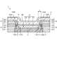
- FIG. 1 is a cross-sectional view of a light emitting device according to the first embodiment.
- the light emitting element 1 according to the present embodiment has an anode electrode 11, a pixel separation insulating film 12, and an organic layer 13.
- the anode electrode 11 is electrically separated for each pixel and also functions as a reflective layer, and it is desirable to have as high a reflectance as possible in order to improve the luminous efficiency. Further, since the anode electrode 11 is used as an anode, it is desirable that the anode electrode 11 is made of a material having high hole injection property.
- the thickness of such an anode electrode 11 in the stacking direction (hereinafter, simply referred to as thickness) is, for example, 30 nm or more and 1000 nm or less.
- the pitch of the anode electrodes 11 (distance between adjacent anode electrodes 11) is, for example, about 200 nm to 1000 nm.
- the constituent materials of the anode electrode 11 include chromium (Cr), gold (Au), platinum (Pt), nickel (Ni), copper (Cu), molybdenum (Mo), tungsten (W), titanium (Ti), and tantalum. Examples include a simple substance or an alloy of a metal element such as (Ta), silver (Ag) or aluminum (Al).
- a transparent conductive film such as an oxide of indium and tin (ITO) may be provided on the surface of the anode electrode 11.
- the thickness of the anode electrode 11 is appropriately set according to the balance between the wiring resistance and the reflectance (surface roughness).
- the anode electrode 11 is composed of a transparent conductive film.
- the pixel separation insulating film 12 is for electrically separating the anode electrode 11 for each pixel and ensuring the insulating property between the anode electrode 11 and the cathode electrode 14 in contact with the organic layer 13.
- the pixel separation insulating film 12 is formed by laminating the lower insulating layer 121, the intermediate insulating layer 122, and the upper insulating layer 123.
- the pixel separation insulating film 12 is an example of an "insulating layer".
- the lower insulating layer 121 has an opening for exposing the surface of the anode electrode 11 (the surface facing the cathode electrode 14) to the outside, and is provided so as to cover the peripheral edge of the anode electrode 11 from the surface to the side surface (end surface).
- the opening of the lower insulating layer 121 is formed in a tapered shape so that the inner wall 121A extending from the surface facing the cathode electrode 14 toward the anode electrode 11 becomes smaller toward the anode electrode 11.
- the intermediate insulating layer 122 is laminated on the surface of the lower insulating layer 121 facing the cathode electrode 14.
- the intermediate insulating layer 122 is arranged at a certain distance from each point on the outer periphery of the opening of the lower insulating layer 121. That is, the intermediate insulating layer 122 has an opening whose outer circumference is located at a certain distance from the opening of the lower insulating layer 121.
- the inner wall 122A of the opening of the intermediate insulating layer 122 according to the present embodiment has a surface perpendicular to the anode electrode 11 in the thickness direction.
- the upper insulating layer 123 is laminated on the surface of the intermediate insulating layer 122 facing the cathode electrode 14.
- the upper insulating layer 123 has an opening in which the inner wall 123A is tapered.
- the opening of the upper insulating layer 123 has a shape in which the outer circumference of the inner wall 123A on the anode electrode 11 side is contracted inward by a certain distance from the outer circumference of the opening of the intermediate insulating layer 122.
- the outer circumference of the inner wall 123A becomes larger in the opening of the upper insulating layer 123 in the direction away from the anode electrode 11.
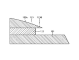
- the portion including the thickness of the inner wall 123A of the upper insulating layer 123 is the eaves 123B as described later. That is, the eaves 123B has a tapered shape.
- the eaves 123B of the upper insulating layer 123 has a smaller thickness or a smaller taper angle with respect to the combined thickness of the inner wall 121A, the inner wall 122A, and the inner wall 123A.
- the maximum angle that can improve the organic attachment of the organic layer 13 corresponds to an example of "predetermined angle".
- the eaves 123B may have a small thickness and a small taper angle.
- the opening 120 of the pixel separation insulating film 12 is formed by the opening of the lower insulating layer 121, the opening of the intermediate insulating layer 122, and the opening of the upper insulating layer 123.
- the opening 120 divides the light emitting region of the light emitting element 1.
- the planar shape of the opening 120 is not particularly limited, but is, for example, a rectangular shape, a square shape, a circular shape, or the like.
- the edge of the opening of the upper insulating layer 123 projects toward the inside of the opening 120 from the edge of the opening of the intermediate insulating layer 122, and the protruding portion is an eaves. It becomes 123B.
- the inner wall 122A of the intermediate insulating layer 122 is formed so as to recede from the position of the end portion of the inner wall 123A of the upper insulating layer 123 on the anode electrode 11 side.
- the eaves 123B By providing the eaves 123B, the first OLED layer 131 and the CGL 132 in the organic layer 13 are cut as described later. Therefore, the shape including the thickness, length and taper angle of the eaves 123B and the shape including the thickness of the intermediate insulating layer 122 are formed by each of the first OLED layer 131 and the CGL 132 when the first OLED layer 131 and the CGL 132 are vapor-deposited. It is determined to be cut at the organic layer cut portion P.
- the height and width of the eaves 123B depend on the thickness, material and etching conditions of the upper insulating layer 123 and the intermediate insulating layer 122, the width of the opening 120, the material and thickness of the first OLED layer 131 and the CGL 132, and the like. Layer 131 and CGL 132 are set to cuttable values.
- the edge of the opening of the lower insulating layer 121 projects toward the inside of the opening 120 from the edge of the opening of the upper insulating layer 123.
- the distance L between the position of the end portion of the inner wall 121A of the lower insulating layer 121 on the anode electrode 11 side and the position of the end portion of the inner wall 123A of the upper insulating layer 123 on the anode electrode 11 side has a certain distance.
- the distance L can be 200 nm. By setting this distance L to a certain length or more, the pixel edge vertical leak can be improved.
- the lower insulating layer 121, the upper insulating layer 123, and the intermediate insulating layer 122 are each capable of obtaining an etching selectivity among inorganic insulating materials such as silicon oxide, silicon nitride, silicon oxynitride, and aluminum oxide. It is composed of different materials.
- the lower insulating layer 121 and the upper insulating layer 123 are formed of silicon oxide (SiO 2 ), and the intermediate insulating layer 122 is formed of silicon nitride (SiN).
- the etching selectivity can be obtained between the lower insulating layer 121, the upper insulating layer 123, and the intermediate insulating layer 122, and different materials from the lower insulating layer 121 and the upper insulating layer 123 may be used. Further, a material capable of obtaining an etching selectivity may be used between the lower insulating layer 121 and the upper insulating layer 123. As described above, by using a material capable of obtaining an etching selectivity, it becomes easy to process the lower insulating layer 121, the upper insulating layer 123, and the intermediate insulating layer 122 into desired shapes, respectively.
- the organic layer 13 includes a laminated first OLED layer 131, a CGL (Charge Generation Layer) 132, and a second OLED layer 133. Although not shown, the organic layer 13 also includes an electron injection layer, an electron transport layer, a hole transport layer, a hole injection layer, and the like.
- the first OLED layer 131 is a blue light emitting layer. When an electric field is applied to the first OLED layer 131, a part of the holes injected from the anode electrode 11 and a part of the electrons injected from the cathode electrode 14 are recombined to emit blue light. ..
- the first OLED layer 131 includes, for example, at least one of a blue light emitting material, a hole transporting material, an electron transporting material, and a bicharge transporting material.
- the blue light emitting material may be fluorescent or phosphorescent.
- the first OLED layer 131 is composed of DPVBi mixed with 2.5% by weight of 4,4'-bis [2- ⁇ 4- (N, N-diphenylamino) phenyl ⁇ vinyl] biphenyl (DPAVBi).
- DPVBi 4,4'-bis [2- ⁇ 4- (N, N-diphenylamino) phenyl ⁇ vinyl] biphenyl
- the first OLED layer 131 is formed by being deposited, for example, by a vapor deposition method. By depositing on the eaves 123B, a region behind the elements deposited on the eaves 123B and the eaves 123B is formed on the surface of the lower insulating layer 121 on the cathode electrode 14 side. The first OLED layer 131 is no longer deposited in the shaded region and is cut by the organic layer cut portion P. Such a phenomenon in which the organic layer is cut by being shaded by the eaves 123B and the elements deposited on the eaves 123B during vapor deposition is sometimes called "shadowing phenomenon in the organic vapor deposition process".
- CGL132 is a charge generation layer formed of a material having high conductivity for supplying carriers, and is a layer having high hole mobility.
- the CGL 132 supplies electrons to the first OLED layer 131, supplies holes to the second OLED layer 133, and supplies an equal amount of electric charge to each of them to maintain an equipotential surface in the CGL 132. Luminous efficiency is increased by CGL132.
- CGL132 is formed by being deposited, for example, by a vapor deposition method.
- the CGL 132 is also a region behind the elements deposited on the eaves 123B and the eaves 123B on the surface of the lower insulating layer 121 on the cathode electrode 14 side. It is not deposited on the organic layer and is cut at the organic layer cut portion P due to the shadowing phenomenon in the organic vapor deposition process.
- the second OLED layer 133 is a red and green light emitting layer. When an electric field is applied to the second OLED layer 133, a part of the holes injected from the anode electrode 11 and a part of the electrons injected from the cathode electrode 14 are recombined to emit red and green light. It emits light.
- the second OLED layer 133 contains, for example, at least one of a red and green light emitting material, a hole transporting material, an electron transporting material, and a bicharge transporting material.
- the red and green light emitting materials may be fluorescent or phosphorescent.
- the second OLED layer 133 is formed by being deposited, for example, by a vapor deposition method.
- the second OLED layer 133 is deposited on each of the CGL 132 laminated on the eaves 123B and the CGL 132 laminated on the anode electrode 11.
- CGL132 is cut by the organic layer cut portion P, but the interval is short. Therefore, the second OLED layer 133 deposited on the CGL 132 laminated on the eaves 123B and the second OLED layer 133 deposited on the picture of the CGL 132 laminated on the anode electrode 11 are connected to each other. That is, the second OLED layer 133 fills the opening of the organic layer cut portion P and becomes one continuous layer.
- the gap S may be filled with the second OLED layer 133.
- the cathode electrode 14 is formed so as to cover the entire surface of the second OLED layer 133 opposite to the anode electrode 11.
- the cathode electrode 14 is composed of, for example, a light-transmitting conductive film, for example, a single-layer film such as ITO, IZO, ZnO, InSnZnO, MgAg alloy and Ag, or a laminated film containing two or more of them. ..
- a light-transmitting conductive film for example, a single-layer film such as ITO, IZO, ZnO, InSnZnO, MgAg alloy and Ag, or a laminated film containing two or more of them. ..
- the same materials as those listed in the anode electrode 11 can be used.
- the organic layer 13 As described above, in the organic layer 13, the first OLED layer 131 which is a blue light emitting layer and the second OLED layer 133 which is a red and green light emitting layer are laminated, and the light generated by each is mixed to generate white light.
- the organic layer 13 is not limited to such a laminated structure as long as it has a structure that generates white light.
- the organic layer 13 may be a stack of a blue light emitting layer and a yellow light emitting layer, or may be a stack of a blue light emitting layer and an orange light emitting layer.
- a display device using the light emitting element 1 will be described.
- a protective layer is generated on the surface of the cathode electrode 14 opposite to the second OLED layer 133.
- the protective layer is made of silicon nitride, silicon oxide, metal oxide, or the like.
- a color filter layer is generated on the side opposite to the cathode electrode 14 of the protective layer.
- the color filter layer extracts the white light generated by the light emitting element 1 as red light, green light, or blue light for each pixel.
- the color filter layer is arranged at a position where, for example, any of the red filter layer, the green filter layer, and the blue filter layer faces the light emitting element 1.
- the light emitting element 1 is manufactured by combining a general semiconductor process. The outline of the light emitting element 1 and an example of the manufacturing process of the display device using the light emitting element 1 will be described below.
- a photosensitive resin is applied to the entire surface.
- the photosensitive resin is exposed and developed and patterned into a predetermined shape to form a flattening layer.
- the plug is formed by embedding the connection hole with a conductive material.
- the metal layer is formed into a film by, for example, a sputtering method, and then wet etching is performed, for example, to form the anode electrode 11 separated for each light emitting element 1 (for each pixel).
- the pixel separation insulating film 12 having the opening 120 and the eaves 123B is generated.
- the lower insulating layer 121, the intermediate insulating layer 122, and the upper insulating layer 123 are laminated in this order over the entire surface of the substrate.
- SiON or SiN is used as the lower insulating layer 121
- SiO 2 is used as the intermediate insulating layer 122
- SiON or SiN is used as the upper insulating layer 123, for example, by a CVD (Chemical Vapor Deposition) method.
- CVD Chemical Vapor Deposition
- the second insulating layer 15B is selectively removed by etching using, for example, a photolithography method, and an opening is made in the upper insulating layer 123.
- a photoresist is formed and exposed (patterned) on the upper insulating layer 123.
- anisotropic (or isotropic) dry etching or wet etching
- the upper insulating layer is used under the condition that the etching selectivity can be obtained between the upper insulating layer 123 and the intermediate insulating layer 122.
- the eaves 123B of the upper insulating layer 123 is preferably formed to be thinner or have a smaller taper angle with respect to the thickness of the inner wall of the opening 120.
- the exposed intermediate insulating layer 122 is selectively removed to form an opening of the intermediate insulating layer 122.
- intermediate insulation is performed using the condition that the etching selectivity can be obtained between the intermediate insulating layer 122 and the upper insulating layer 123 and the lower insulating layer 121 by, for example, isotropic dry etching or isotropic wet etching.
- the layer 122 is processed to the surface of the lower insulating layer 121.
- the opening of the intermediate insulating layer 122 is formed, and the position of the inner wall 122A of the intermediate insulating layer 122 is retracted from the end of the inner wall 123A of the upper insulating layer 123 on the intermediate insulating layer 122 side to form the eaves 123B. Will be done.
- the exposed lower insulating layer 121 is selectively removed to form the opening 120.
- the lower insulating layer 121 is subjected to the anode electrode under the condition that the etching selectivity between the lower insulating layer 121 and the intermediate insulating layer 122 can be obtained by, for example, isotropic dry etching or isotropic wet etching. Process up to the surface of 11. At this time, etching is performed so that the inner wall 121A of the lower insulating layer 121 has a tapered shape.
- the distance L between the end of the inner wall 121A of the lower insulating layer 121 on the anode electrode 11 side and the end of the inner wall 123A of the upper insulating layer 123 on the anode electrode 11 side is formed to have a certain length.
- the hole injection layer and the hole transport layer are formed on the entire surface of the substrate in this order by, for example, a vacuum deposition method, a sputtering method, or a coating method such as a spin coating method or a die coating method.
- the hole injection layer is cut by the eaves 123B formed in the opening 120 of the pixel separation insulating film 12.
- the first OLED layer 131 is formed into a film by, for example, a vacuum deposition method, a sputtering method, or a coating method such as a spin coating method or a die coating method. At this time, the first OLED layer 131 is cut by the eaves 123B formed in the opening 120 of the pixel separation insulating film 12.
- the CGL 132 is formed into a film by, for example, a vacuum deposition method, a sputtering method, or a coating method such as a spin coating method or a die coating method. At this time, the CGL 132 is cut by the eaves 123B formed in the opening 120 of the pixel separation insulating film 12.
- the first OLED layer 131 and the CGL 132 can be separately formed for each anode electrode 11 by the eaves 123B without separately patterning.
- the second OLED layer 133 is formed into a film by, for example, a vacuum deposition method, a sputtering method, or a coating method such as a spin coating method or a die coating method.
- the second OLED layer 133 is formed in a connected state without being cut by the eaves 123B.
- the gap S is formed by filling the cut portion of the first OLED layer 131 and the CGL 132 with the second OLED layer 133.
- a cathode electrode 14 made of the above-mentioned material is formed on the entire surface of the substrate by, for example, a vacuum vapor deposition method or a sputtering method.
- the organic layer 13 and the cathode electrode 14 can be continuously formed on the anode electrode 11 in, for example, a vacuum atmosphere.
- the organic layer 13 and the cathode electrode 14 have an element structure formed not only in the region directly above the anode electrode 11 but also in the region between the adjacent anode electrodes 11 (between pixels). In this way, the light emitting element 1 is formed.
- a protective layer is formed on the light emitting element 1 by, for example, a CVD method or a sputtering method. Further, a sealing substrate having a color filter layer is attached onto the protective layer via an adhesive layer. As a result, a display device having the light emitting element 1 can be manufactured.
- FIG. 2 is a diagram of one embodiment of the light emitting device according to the first embodiment.
- the pixel separation insulating film 12 has a lower insulating layer 121 having an opening 120, an intermediate insulating layer 122, and an upper insulating layer 123.
- the eaves 123B are formed by recessing the intermediate insulating layer 122 with respect to the center of the opening 120 with respect to the upper insulating layer 123.
- the first OLED layer 131 and the CGL 132 are cut. Further, in the case of the embodiment of FIG. 2, the void S is formed.
- a drive current is injected.
- this drive current is injected into the first OLED layer 131 and the second OLED layer 133 of the organic layer 13 through the anode electrode 11 and the cathode electrode 14 via the CGL 132, the holes and electrons are recombined and light emission occurs. ..
- the white light generated from the organic layer 13 and passed through the cathode electrode 14 is color-separated into, for example, RGB (Red Green Blue) in the color filter layer. That is, of the white light generated from the light emitting element 1, red light is selectively transmitted through the red filter layer, green light is selectively transmitted through the green filter layer, and blue light is selectively transmitted through the blue filter layer.
- RGB Red Green Blue
- the organic layer 13 and the cathode electrode 14 are continuously solid-formed without being patterned for each pixel.
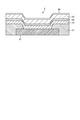
- FIG. 3 is a cross-sectional view of a light emitting element having continuous CGLs.
- the light emitting element 2 has an anode electrode 21, a pixel separation insulating film 22, a first OLED layer 23, a CGL 24, a second OLED layer 25, and a cathode electrode 26, similarly to the light emitting element 1 according to the present embodiment.
- the pixel separation insulating film 22 has no eaves at the intermediate position of the inner wall of the opening. Therefore, as shown in FIG. 3, in the conventional light emitting element 2, the first OLED layer 23 and the CGL 24 are not cut for each anode electrode 21 (for each pixel). Therefore, in the CGL 24, which is a layer having high hole mobility, adjacent pixels are electrically connected.
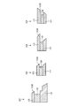
- FIG. 4 is a diagram for explaining the influence of the leak current on the CGL.
- Section 301 represents a state in which a current flows through the anode electrode 21A corresponding to the red filter layer 27A.
- Section 302 represents a state in which a current flows through the anode electrode 21B corresponding to the green filter layer 27B.
- Section 303 represents a state in which a current flows through the anode electrode 21C corresponding to the blue filter layer 27C.
- the eaves 123B are provided at the intermediate position of the inner wall of the opening 120 of the pixel separation insulating film 12, and the first OLED layer 131 and the CGL 132 are cut by the eaves 123B.
- the organic layer 13 and the cathode electrode 14 are continuously solid-formed on the anode electrode 11, but the CGL 132 is electrically cut off between adjacent pixels.
- the CGL 132 can be electrically cut off between each pixel.
- current leakage can be suppressed in a structure in which the organic layer 13 is continuously solid-formed on all pixels.
- charge injection efficiency here, hole injection efficiency
- light emission efficiency can be improved.
- the current leakage to the adjacent pixels is reduced, the occurrence of color mixing can be suppressed.
- FIG. 5 is a diagram showing an outline of a cross section of the pixel separation insulating film according to the first modification of the first embodiment.
- the pixel separation insulating films 12 represented by the cross sections 201 to 204 in FIG. 5 have different shapes of the intermediate insulating layers 122.
- the inner wall 122A at the opening of the intermediate insulating layer 122 has a tapered shape so as to be perpendicular to the surface of the anode electrode 11.
- the shape of the pixel separation insulating film 12 of the light emitting element 1 according to the first embodiment is referred to as a standard shape.
- the inner wall 122A in the cross section 201 has a tapered shape in which the opening increases from the cathode electrode 14 side to the anode electrode 11 side, that is, a reverse taper shape of the eaves 123B.
- the position of the end of the opening of the intermediate insulating layer 122 on the cathode electrode 14 side is a position farther from the center of the opening than the position of the end of the opening of the upper insulating layer 123 on the anode electrode 11 side.
- the inner wall 122A in the cross section 202 has an inverted tapered shape of the eaves 123B as in the cross section 201.
- the position of the end portion of the opening of the intermediate insulating layer 122 on the cathode electrode 14 side coincides with the position of the end portion of the opening of the upper insulating layer 123 on the anode electrode 11 side.
- the inner wall 122A in the cross section 203 has a tapered shape in which the opening becomes smaller from the cathode electrode 14 side toward the anode electrode 11 side, that is, a forward taper shape of the eaves 123B.
- the position of the end of the opening of the intermediate insulating layer 122 on the cathode electrode 14 side is a position farther from the center of the opening than the position of the end of the opening of the upper insulating layer 123 on the anode electrode 11 side.
- the inner wall 122A in the cross section 204 has a shape that is concave with respect to the center of the opening. Then, in FIG. 5, the position of the end portion of the opening of the intermediate insulating layer 122 on the cathode electrode 14 side coincides with the position of the end portion of the opening of the upper insulating layer 123 on the anode electrode 11 side. However, the position of the end portion of the opening of the intermediate insulating layer 122 on the cathode electrode 14 side may be a position farther from the center of the opening than the position of the end portion of the opening of the upper insulating layer 123 on the anode electrode 11 side.
- any of the cross sections 201 to 204 can be used. Regardless of the shape of the cross section 201 to 204, the first OLED layer 131 and the CGL 132 are cut by the shadowing phenomenon in the organic vapor deposition process.
- the light emitting element 1 according to the present modification has a pixel separation insulating film 12 having a shape different from the standard shape, and even if such a pixel separation insulating film 12, the CGL 132 has a shape different from the standard shape. Be disconnected. Therefore, the current leakage can be suppressed, the excitation light emission in the pixels other than the applied pixel can be suppressed, and the light emission characteristics can be improved.
- the shape of the pixel separation insulating film 12 is not particularly limited as long as the CGL 132 can be cut by the shadowing phenomenon in the organic vapor deposition process by providing the eaves 123B.
- FIG. 6 is a diagram showing a cross section of the pixel separation insulating film according to the second modification of the first embodiment.
- the distance from the opening-side end of the upper insulating layer 123 to the opening-side end of the lower insulating layer 121 is the pixel separation shown in FIG. It is formed longer than the insulating film 12 for use.
- the coating properties of the second OLED layer 133, the cathode electrode 14, and the protective film are deteriorated. Can be improved.
- FIG. 7 is a diagram showing a cross section of the pixel separation insulating film according to the third modification of the first embodiment.
- the light emitting element 1 according to this modification is formed so that the thickness of the upper insulating layer 123 is thicker than the thickness of the upper insulating layer 123 of the pixel separation insulating film 12 shown in FIG. ..
- the taper angle of the inner wall 123A is smaller than the taper angle of the inner wall 123A of the pixel separation insulating film 12 shown in FIG.
- the pixel separation insulating film 12 of the light emitting element 1 selects whether to thin the upper insulating layer 123 or lower the taper angle of the inner wall 123A in order to cut the first OLED layer 131 and the CGL 132. Is possible.
- the light emitting element 1 according to the present embodiment is different from the first embodiment in that a layer is added to the pixel separation insulating film 12 in addition to the lower insulating layer 121, the intermediate insulating layer 122, and the upper insulating layer 123.
- the light emitting element 1 according to the present embodiment has a structure similar to that shown in FIG. 1 except for the shape of the pixel separation insulating film 12.
- FIG. 8 is a cross-sectional view of the image separation insulating film according to the second embodiment.
- the pixel separation insulating film 12 according to the present embodiment has the lowest insulating layer 124 under the lower insulating layer 121.
- the opening 120 of the pixel separation insulating film 12 is formed including the opening of the lowest insulating layer 124.
- the inner wall at the opening of the lowermost insulating layer 124 has a region farther from the center of the opening 120 than the end of the inner wall at the opening of the lower insulating layer 121 on the anode electrode 11 side.
- the inner wall at the opening of the lowermost insulating layer 124 has a region recessed from the end of the inner wall at the opening of the lower insulating layer 121 on the anode electrode 11 side with respect to the center of the opening 120.
- a part of the lower insulating layer 121 is formed as the eaves 121B.
- the height of the eaves 121B may be set to a value as small as possible that can cut the hole injection layer arranged on the anode electrode 11 side of the first OLED layer 131 in the organic layer 13. desirable.
- the height and width of the eaves 121B depend on the thickness, material and etching conditions of the lower insulating layer 121 and the lowest insulating layer 124, the width of the opening 120, the material and thickness of the hole injection layer, and the like.
- the layer is set to a value that can be cut.
- the layer cut by the lowest insulating layer 124 is not limited to the hole injection layer, and other layers of the organic layer 18 may be cut.
- the lowest insulating layer 124 is formed by the following method. By selectively removing the lower insulating layer 121, an opening is formed and the lowermost insulating layer 124 is exposed. Subsequently, the exposed lowest insulating layer 124 is selectively removed to form an opening of the lowest insulating layer 124. At this time, for example, by isotropic dry etching or isotropic wet etching, the lowest insulating layer 124 is formed by using the condition that the etching selectivity can be obtained between the lowermost insulating layer 124 and the lower insulating layer 121. The surface of the anode electrode 11 is processed.
- This eaves 121B corresponds to an example of "the eaves for cutting the lower end layer".
- the hole injection layer of the organic layer 13 is cut by the shadowing phenomenon in the organic vapor deposition process at the time of vapor deposition because the lowermost insulating layer 124 is provided to form the eaves 121B. That is, the hole injection layer of the organic layer 13 is cut for each anode electrode 11 (for each pixel).
- the hole injection layer is cut by the eaves 121B, but if the positive electrode and the negative electrode have opposite structures, the electron injection layer in the organic layer 13 is cut by the eaves 121B. That is, the hole injection layer or the electron injection layer is a layer located at the end of the organic layer 13, and the side located on the anode electrode 11 side becomes the lower end layer and is cut by the eaves 121B.
- the first OLED layer 131 and the CGL 132 are cut by the shadowing phenomenon in the organic thin-film deposition process at the time of vapor deposition by the eaves 123B, as in the first embodiment.
- the light emitting element 1 has a hole injection layer cut for each pixel.
- the hole injection layer 17 can be electrically blocked between each pixel. Therefore, it is possible to suppress current leakage in an element structure having a light emitting layer common to all pixels. Further, since the current leakage in the hole injection layer can be suppressed, the hole injection layer can be thickened, so that the hole injection efficiency and thus the luminous efficiency can be further improved.
- the light emitting element 1 according to this modification has a pixel separation insulating film 12 corresponding to three or more light emitting layers.
- FIG. 9 is a diagram showing an outline of a cross section of the pixel separation insulating film according to the modified example of the second embodiment.
- the pixel separation insulating film 12 of the light emitting element 1 according to this embodiment has a shape represented by a cross section 212 or 213.
- the pixel separation insulating film 12 having a cross section 212 has a second middle insulating layer 125 and a second upper insulating layer 126 on the upper insulating layer 123.
- the inner wall of the second middle-stage insulating layer 125 is located at a position farther from the center of the opening 120 than the end portion of the second upper-stage insulating layer 126 on the second middle-stage insulating layer 125 side. As a result, a part of the second upper insulating layer 126 is formed as the eaves 126B.
- the second middle-stage insulating layer 125 and the second upper-stage insulating layer 126 are manufactured by the same procedure as the manufacturing procedure of the intermediate-stage insulating layer 122 and the upper-stage insulating layer 123 described in the first embodiment.
- the organic layer 13 has three stages of OLED layers.
- the three-stage OLED layer is referred to as a first-stage layer, a second-stage layer, and a third-stage layer from the anode electrode 11 side, respectively.
- the first CGL is laminated between the first layer and the second layer
- the second CGL is laminated between the second layer and the third layer.
- the first layer and the first CGL are cut for each anode electrode 11 (for each pixel) due to the shadowing phenomenon in the organic vapor deposition process due to the provision of the eaves 123B. Further, the second layer and the second CGL are cut for each anode electrode 11 (for each pixel) due to the shadowing phenomenon in the organic vapor deposition process due to the provision of the eaves 126B.
- the pixel separation insulating film 12 having a cross section 213 has a second middle-stage insulating layer 125, a second upper-stage insulating layer 126, a third middle-stage insulating layer 127, and a third upper-stage insulating layer 128 on the upper-stage insulating layer 123.
- the inner wall of the second middle-stage insulating layer 125 is located at a position farther from the center of the opening 120 than the end portion of the second upper-stage insulating layer 126 on the second middle-stage insulating layer 125 side. As a result, a part of the upper insulating layer 123 is formed as the eaves 126B.
- the inner wall of the third middle-stage insulating layer 127 is located at a position farther from the center of the opening 120 than the end portion of the third upper-stage insulating layer 128 on the third middle-stage insulating layer 127 side. As a result, a part of the third upper insulating layer 128 is formed as the eaves 128B.
- the second middle-stage insulating layer 125 and the second upper-stage insulating layer 126, and the third middle-stage insulating layer 127 and the third upper-stage insulating layer 128 are the manufacture of the intermediate-stage insulating layer 122 and the upper-stage insulating layer 123 described in the first embodiment. Manufactured in the same procedure as the procedure.
- the organic layer 13 has four stages of OLED layers.
- the four-stage OLED layer is referred to as a first-stage layer, a second-stage layer, a third-stage layer, and a fourth-stage layer from the anode electrode 11 side, respectively.
- the first CGL is laminated between the first layer and the second layer
- the second CGL is laminated between the second layer and the third layer
- the third layer and the fourth stage are laminated.
- a third CGL is laminated between the layers.
- the first layer and the first CGL are cut for each anode electrode 11 (for each pixel) due to the shadowing phenomenon in the organic vapor deposition process due to the provision of the eaves 123B. Further, the second layer and the second CGL are cut for each anode electrode 11 (for each pixel) due to the shadowing phenomenon in the organic vapor deposition process due to the provision of the eaves 126B. Further, the third layer and the third CGL are cut for each anode electrode 11 (for each pixel) due to the shadowing phenomenon in the organic vapor deposition process due to the provision of the eaves 128B.
- the pixel separation insulating film 12 having a shape corresponding to the organic layer 13 having the three-stage OLED layer or the four-stage OLED layer has been described, but the number of stages of the OLED layer is particularly high. There is no limitation, and the pixel separation insulating film 12 may be provided with eaves according to the number of stages of the OLED layer.
- the light emitting element 1 cuts each CGL of the three or more stages of the OLED layer and the organic layer 13 having the CGL for each pixel. As a result, current leakage in CGL can be suppressed. Therefore, it is possible to suppress excitation light emission in pixels other than the applied pixel, and it is possible to improve the light emission characteristics.
- the pixel separation insulating film 12 having the same number of eaves as the CGL to be cut has been described, but there is a CGL that is cut by the inclination of the inner wall in the opening 120 including the eaves in the CGL. In this case, it is not necessary to provide the eaves corresponding to the CGL. That is, when the CGL to be cut has a CGL to be cut due to the inclination of the inner wall of the opening 120, the number of eaves obtained by subtracting the number of CGLs from the total number of CGLs to be cut is the pixel separation insulating film 12 It may be provided in.
- FIG. 10 is a cross-sectional view of the pixel separation insulating film according to the third embodiment.
- the pixel separation insulating film 12 of the light emitting element 1 according to the present embodiment has a structure represented by any of the cross sections 221 to 224.
- the light emitting element 1 according to the present embodiment has a structure similar to that shown in FIG. 1 except for the shape of the pixel separation insulating film 12.
- the pixel separation insulating film 12 having a cross section 221 has the following structure.
- the lower insulating layer 121 has a stepped opening with two steps.
- the lower insulating layer 121 is formed so that the step on the cathode electrode 14 side is recessed with respect to the center of the opening rather than the break on the anode electrode 11 side.
- the inner wall of the lower insulating layer 121 at the opening of the stage on the anode electrode 11 side has a tapered shape in which the opening becomes smaller toward the anode electrode 11.
- the pixel separation insulating film 12 having a cross section 222 is arranged so that the ends of the openings of the lower insulating layer 121 and the upper insulating layer 123 coincide with each other.
- the end of the opening of the upper insulating layer 123 is arranged at a position closer to the center of the opening than the end of the lower insulating layer 121.
- the pixel separation insulating film 12 having a cross section of 224 has a tapered shape in which the inner wall at the opening of the upper insulating layer 123 and the lower insulating layer 121 becomes larger toward the anode electrode 11. Further, the end of the opening of the upper insulating layer 123 is arranged at a position closer to the center of the opening than the end of the lower insulating layer 121.
- Each of the light emitting elements 1 according to the present embodiment provided with the pixel separation insulating film 12 having any of the cross sections 221 to 224 has an eaves 123B at an intermediate position of the inner wall of the pixel separation insulating film 12.
- the light emitting element 1 according to the present embodiment has the CGL 132 cut for each anode electrode 11 (for each pixel).
- the organic film is poorly attached, a thin organic structure is generated with respect to the flat portion of the pixel opening, the OLED voltage of that portion becomes low, and the organic device is in the vertical direction in the low voltage region. Current leakage may occur. Therefore, if deterioration of the organic film formed on the stepped portion of the pixel separation insulating film 12 is permissible, the light emitting element 1 according to the present embodiment is used to suppress current leakage and apply pixels. Excitation light emission in pixels other than the above can be suppressed, and light emission characteristics can be improved.
- the light emitting element 1 according to the present embodiment has a pixel separation insulating film 12 in which the shape of a portion other than the eaves 123B is modified as in the cross section 221.
- the light emitting element 1 according to the present embodiment has a structure similar to that shown in FIG. 1 except for the shape of the pixel separation insulating film 12.
- FIG. 11 is a diagram showing a cross section of the pixel separation insulating film according to the fourth embodiment.
- the light emitting element 1 according to this embodiment includes a pixel separation insulating film 12 having either a cross section of 231 or 232.
- the pixel separation insulating film 12 having the cross section 231 is obtained by deforming the shape of the lower insulating layer 121 of the cross section 211 shown in FIG. 8 in the same manner as the lower insulating layer 121 of the cross section 211 shown in FIG.
- deforming the shape of the lower insulating layer 121 the deposition state of the organic element below the eaves 123B can be changed, and the relationship between the height of the eaves 123B and the cut portion of the organic layer 13 can be changed.
- the hole injection layer is cut by the shadowing phenomenon in the organic vapor deposition due to the provision of the eaves 121B. Further, by changing the shape of the lower insulating layer 121 to control the cutting state of the organic layer 13, the shadowing phenomenon in the organic vapor deposition due to the provision of the eaves 123B ensures that the first OLED layer 131 and the CGL 132 are deposited. Is disconnected. That is, the light emitting element 1 provided with the pixel separation insulating film 12 having a cross section 231 has a first OLED layer 131 and a CGL 132 that are surely cut for each anode electrode 11 (for each pixel).
- the pixel separation insulating film 12 having the cross section 232 is deformed in the same manner as the upper insulating layer 123 of the cross section 211 shown in FIG. 10 in the shape of the upper insulating layer 123 of the cross section 212 and the second upper insulating layer 126 shown in FIG. It was made to do.
- the deposition state of the organic element below the eaves 123B can be changed, and by deforming the shape of the upper insulating layer 123, the organic element below the eaves 126B can be changed.
- the deposition state of the eaves 123B and 126B can be changed, and the relationship between the height of the eaves 123B and 126B and the cut portion of the organic layer 13 can be changed.
- the organic layer 13 has a three-stage light emitting layer called a first-stage layer, a second-stage layer, and a third-stage layer, and the first CGL and the second CGL are laminated between the layers. explain.
- the light emitting element 1 provided with the pixel separation insulating film 12 having a cross section of 232 is surely cut for each anode electrode 11 (for each pixel) with respect to the organic layer 13 having three stages of light emitting layers. It has an anode layer, a first CGL, a second layer, and a second CGL.
- the light emitting element 1 provided with the pixel separation insulating film 12 having a cross section 231 or 232 has been described.
- the cutting state of the organic layer 13 can be controlled by changing the shape of the lower insulating layer 121.
- the light emitting element 1 deforms the shape other than the eaves 123B, so that the cut state of the organic layer 13 due to the shadowing phenomenon in the organic vapor deposition due to the provision of the eaves structure can be obtained. Control.
- the layer contained in the target organic layer 13 can be reliably cut, current leakage can be suppressed more reliably, excitation light emission in pixels other than the applied pixels can be suppressed, and light emission characteristics can be improved. can do.
- One lower insulating layer 121 is continuously arranged between the adjacent anode electrodes 11. That is, the lower insulating layer 121 that covers the surface near the end of one anode electrode 11 extends to cover the vicinity of the end of the adjacent anode electrode 11.
- two intermediate insulating layers 122 are arranged between the adjacent anode electrodes 11.
- the upper insulating layer 123 is individually arranged on the surface of each intermediate insulating layer 122 on the cathode electrode 14 side. That is, two upper insulating layers 123 are also arranged between the adjacent anode electrodes 11.
- the first OLED layer 131 is cut between the anode electrode 11 and the adjacent upper insulating layer 123 due to the shadowing phenomenon in the organic vapor deposition process by the eaves 123B. Further, the first OLED layer 131 is cut between the two upper insulating layers 123 and the lower insulating layer 121 placed between the adjacent anode electrodes 11 due to the shadowing phenomenon in the organic vapor deposition process by the eaves 123B. ..
- the CGL 132 is also cut between the anode electrode 11 and the adjacent upper insulating layer 123 due to the shadowing phenomenon in the organic vapor deposition process by the eaves 123B. Further, the CGL 132 is also cut between the two upper insulating layers 123 and the lower insulating layer 121 placed between the adjacent anode electrodes 11 by the shadowing phenomenon in the organic vapor deposition process by the eaves 123B.
- the second OLED layer 133 is formed as a continuous layer without being cut between each pixel.
- the light emitting element 1 As described above, in the light emitting element 1 according to the present embodiment, a plurality of intermediate insulating layers 122 and an upper insulating layer 123 are arranged between adjacent anode electrodes 11 (between pixels). In this way, even if the intermediate insulating layer 122 and the upper insulating layer 123 are interrupted between the adjacent anode electrodes 11, if the eaves structure exists on the anode electrode 11 side, the light emitting element 1 can be used for each anode electrode 11 (between pixels). It is possible to have a CGL 132 cut at every). Therefore, the light emitting element 1 according to the present embodiment can also suppress the current leakage and suppress the excitation light emission in the pixels other than the applied pixel, and can improve the light emission characteristics.
- the light emitting element 1 according to the present embodiment is different from the first embodiment in that the lower insulating layer 121 is not provided.
- the light emitting element 1 according to the present embodiment has a structure similar to that shown in FIG. 1 except for the lower insulating layer 121.
- FIG. 13 is a cross-sectional view of the light emitting element according to the sixth embodiment.
- the lower insulating layer 121 is not arranged in the light emitting element 1 according to the present embodiment. That is, a flat insulating layer is arranged between the side surface of the end portion of one anode electrode 11 and the side surface of the end portion of the adjacent anode electrode 11, and the surface near the end portion of the anode electrode 11 is not covered.
- the intermediate insulating layer 122 is arranged on a flat insulating layer that covers between the adjacent anode electrodes 11. Further, the upper insulating layer 123 is arranged on the surface of each intermediate insulating layer 122 on the cathode electrode 14 side.
- the first OLED layer 131 is cut between the anode electrode 11 by the upper insulating layer 123 and the adjacent upper insulating layer 123 due to the shadowing phenomenon in the organic vapor deposition process by the eaves 123B.
- the CGL 132 is also cut between the anode electrode 11 and the adjacent upper insulating layer 123 by the shadowing phenomenon in the organic vapor deposition process by the eaves 123B.
- the second OLED layer 133 is formed as a continuous layer without being cut between each pixel.
- the light emitting element 1 according to the present embodiment does not have the lower insulating layer 121, and the intermediate insulating layer 122 and the upper insulating layer 123 are arranged between the anode electrodes 11.
- the light emitting element 1 can have the CGL 132 cut for each anode electrode 11 (for each pixel). .. Therefore, the light emitting element 1 according to the present embodiment can also suppress the current leakage and suppress the excitation light emission in the pixels other than the applied pixel, and can improve the light emission characteristics.
- the intermediate insulating layer 122 and the upper insulating layer 123 are arranged with the anode electrode 11 interposed therebetween.
- the structure of the organic layer 13 has the same arrangement as the structure shown in FIG.
- FIG. 14 is a cross-sectional view of the light emitting element according to the seventh embodiment.
- the light emitting element 1 is in close contact with the side surface of the anode electrode 11, and the intermediate insulating layer 122 and the upper insulating layer 123 are arranged.
- the intermediate insulating layer 122 and the upper insulating layer 123 have an opening between the adjacent anode electrodes 11.
- the end of the intermediate insulating layer 122 on the opening side is located farther from the center of the opening than the end of the inner wall of the opening of the upper insulating layer 123 on the anode electrode 11 side.
- the eaves 123B are formed from the anode electrode 11 toward the outside, in other words, toward the adjacent anode electrode 11.
- the first OLED layer 131 is cut between the upper insulating layer 123 and the insulating layer covering between the anode electrodes 11 due to the shadowing phenomenon in the organic vapor deposition process by the eaves 123B.
- the CGL 132 is also cut between the upper insulating layer 123 and the insulating layer covering between the anode electrodes 11 due to the shadowing phenomenon in the organic vapor deposition process by the eaves 123B.
- the second OLED layer 133 is formed as a continuous layer without being cut between each pixel.
- the intermediate insulating layer 122 and the upper insulating layer 123 are arranged so as to sandwich the anode electrode 11, and the eaves 123B are formed toward the outside of the anode electrode 11.
- the light emitting element 1 has a CGL 132 cut for each anode electrode 11 (for each pixel). be able to. Therefore, the light emitting element 1 according to the present embodiment can also suppress the current leakage and suppress the excitation light emission in the pixels other than the applied pixel, and can improve the light emission characteristics.
- the present technology can also have the following configuration.
- the insulating layer has a plurality of the eaves and has a plurality of the eaves.
- the opening-side end of the eaves is separated from the opening-side end of the insulating layer located on the first electrode side of the eaves by a predetermined distance in a direction away from the center of the opening (1).
- the distance from the center of the opening coincides with the opening-side end of the eaves and the opening-side end of the insulating layer located closer to the first electrode than the eaves (1) to (5). ).
- the light emitting element according to any one of. (8)
- the end of the eave on the opening side is closer to the center of the opening than the end of the insulating layer on the opening side of the insulating layer located closer to the first electrode side of the eave (1) to (5).
- the light emitting element according to any one of the above. (9) The light emitting element according to any one of (1) to (8), wherein the insulating layer has a stepped region located on the first electrode side of the eaves.
- a plurality of the light emitting elements are arranged side by side.
- the first electrode is any one of (1) to (10) in which a surface opposite to the opening direction sinks into a region of the insulation layer at the opening located on the side of the first electrode side of the eaves.
Landscapes
- Physics & Mathematics (AREA)
- Optics & Photonics (AREA)
- Engineering & Computer Science (AREA)
- Microelectronics & Electronic Packaging (AREA)
- General Physics & Mathematics (AREA)
- Electroluminescent Light Sources (AREA)
- Optical Filters (AREA)
- Devices For Indicating Variable Information By Combining Individual Elements (AREA)
Abstract
Description
アクティブOLEDは高精細のため、画素塗り分けが難しい。このため、有機蒸着を行う際にはエリア成膜が行われる。この方法では、ホール移動度が高い有機層部分で隣接画素間のリーク電流が問題となる。リーク電流発生の主な原因には、有機層内のホール電子移動度の高い層における画素間での横方向へのリークや、有機被膜性悪化による層の薄い部分の電圧が低くなることによる縦方向へのリークがある。
図1は、第1の実施形態に係る発光素子の断面図である。図1に示すように、本実施形態に係る発光素子1は、アノード電極11、画素分離用絶縁膜12及び有機層13を有する。
発光素子1は、一般的な半導体プロセスを組み合わせることで製造される。以下に、発光素子1及び発光素子1を用いた表示装置の製造工程の一例の概略を説明する。
本実施形態の発光素子1では、駆動電流が注入される。この駆動電流が、アノード電極11及びカソード電極14を通じてCGL132を介して有機層13の第1OLED層131及び第2OLED層133に注入されることにより、正孔と電子とが再結合し、発光が起こる。
本変形例に係る発光素子1は、中間絶縁層122の形状が第1の実施形態と異なる。図5は、第1の実施形態の変形例1に係る画素分離用絶縁膜の断面の概要を表す図である。図5における断面201~204で表される画素分離用絶縁膜12は、それぞれ異なる中間絶縁層122の形状を有する。
図6は、第1の実施形態の変形例2に係る画素分離用絶縁膜の断面を表す図である。本変形例に係る発光素子1は、図6に示すように、上段絶縁層123の開口側の端部から下段絶縁層121の開口側の端部までの距離が、図1に示した画素分離用絶縁膜12よりも長く形成されている。
図7は、第1の実施形態の変形例3に係る画素分離用絶縁膜の断面を表す図である。本変形例に係る発光素子1は、図7に示すように、上段絶縁層123の厚みが、図1に示した画素分離用絶縁膜12の上段絶縁層123の厚みよりも厚く形成されている。さらに、内壁123Aのテーパー角が図1に示した画素分離用絶縁膜12の内壁123Aのテーパー角よりも小さい。
次に、第2の実施形態について説明する。本実施形態に係る発光素子1は、下段絶縁層121、中間絶縁層122及び上段絶縁層123に加えてさらに画素分離用絶縁膜12に層が追加されたことが第1の実施形態と異なる。本実施形態に係る発光素子1は、画素分離用絶縁膜12の形状以外は、図1で示した構造と同様の構造を有する。
本変形例に係る発光素子1は、3段以上の発光層に対応する画素分離用絶縁膜12を有する。図9は、第2の実施形態の変形例に係る画素分離用絶縁膜の断面の概要を表す図である。本実施例に係る発光素子1の画素分離用絶縁膜12は、断面212又は213で表される形状を有する。
図10は、第3の実施形態に係る画素分離用絶縁膜の断面図である。本実施形態に係る発光素子1の画素分離用絶縁膜12は、断面221~224のいずれかで表される構造を有する。本実施形態に係る発光素子1は、画素分離用絶縁膜12の形状以外は、図1で示した構造と同様の構造を有する。
第3の実施形態における断面221のように庇123B以外の形状を変形させることで、庇構造を設けたことによる有機蒸着でのシャドーイング現象による有機層13の切断状態を制御することができる。本実施形態に係る発光素子1は、断面221と同様に庇123B以外の部分の形状を変形させた画素分離用絶縁膜12を有する。本実施形態に係る発光素子1は、画素分離用絶縁膜12の形状以外は、図1で示した構造と同様の構造を有する。
以上の各実施形態では、隣接するアノード電極11の間(画素間)において連続する1つの下段絶縁層121、中間絶縁層122及び上段絶縁層123を有する場合を想定して説明した。これに対して、本実施形態では、隣接するアノード電極11の間(画素間)に複数の中間絶縁層122及び上段絶縁層123を設ける。本実施形態に係る発光素子1は、図1で示した構造と同様の構造を有する。図12は、第5の実施形態に係る発光素子の断面図である。
本実施形態に係る発光素子1は、下段絶縁層121を設けないことが実施例1と異なる。本実施形態に係る発光素子1は、下段絶縁層121以外は、図1で示した構造と同様の構造を有する。図13は、第6の実施形態に係る発光素子の断面図である。
本実施形態に係る発光素子1は、アノード電極11を挟んで中間絶縁層122及び上段絶縁層123が配置される。本実施形態に係る発光素子1は、有機層13の構造は図1で示した構造と同様の配置を有する。図14は、第7の実施形態に係る発光素子の断面図である。
(1)
画素毎に設けられた複数の第1電極と、
前記複数の第1電極のそれぞれを外部に露出する開口を有し、前記開口における内壁の厚み方向の中間位置に庇を有する絶縁層と、
前記絶縁層の前記庇により切断された電荷生成層を含む前記開口を覆う有機層と、
前記有機層の前記第1電極とは逆側の面に配置された第2電極と
を備えた発光素子。
(2)
前記庇は、テーパー状である(1)に記載の発光素子。
(3)
前記庇は、最大の厚みが前記内壁の厚みに比べて薄い又はテーパー角が所定角度以下である(2)に記載の発光素子。
(4)
前記絶縁層は、複数の前記庇を有し、
前記電荷生成層は、前記庇に対応して同数存在し、対応する各前記庇によりそれぞれが切断される(1)~(3)のいずれか一つに記載の発光素子。
(5)
前記絶縁層は、前記内壁の傾斜により切断される前記電荷生成層を含む(4)に記載の発光素子。
(6)
前記庇の前記開口側の端部は、前記庇よりも前記第1電極側に位置する前記絶縁層の開口側の端部に対して、前記開口の中央から離れる方向に所定距離離れる(1)~(5)のいずれか一つに記載の発光素子。
(7)
前記庇の前記開口側の端部が、前記庇よりも前記第1電極側に位置する前記絶縁層の開口側の端部と、前記開口の中央からの距離が一致する(1)~(5)のいずれか一つに記載の発光素子。
(8)
前記庇の前記開口側の端部が、前記庇よりも前記第1電極側に位置する前記絶縁層の開口側の端部よりも前記開口の中央に近くに存在する(1)~(5)のいずれか一つに記載の発光素子。
(9)
前記絶縁層は、前記庇よりも前記第1電極側に位置する領域が階段状である(1)~(8)のいずれか一つに記載の発光素子。
(10)
前記絶縁層は、厚み方向の前記第1電極側の端部に下端層切断用庇を有する(1)~(9)のいずれか一つに記載の発光素子。
(11)
前記発光素子は、複数並び、
前記庇は、前記発光素子間に複数配置される(1)~(10)のいずれか一つに記載の発光素子。
(12)
前記第1電極は、前記開口における前記絶縁層の前記庇よりも前記第1電極側に位置する領域に開口方向とは逆側の面が沈み込む(1)~(10)のいずれか一つに記載の発光素子。
(13)
前記第1電極は、前記庇が前記第1電極から離れる方向に向くように、前記庇の間に挟まれる(1)~(10)のいずれか一つに記載の発光素子。
(14)
基板と、
前記基板上に画素毎に設けられた複数の第1電極と、
前記複数の第1電極のそれぞれを外部に露出する開口を有し、前記開口における内壁の厚み方向の中間位置に庇を有する絶縁層と、
前記絶縁層の前記庇により切断された電荷生成層を含む前記開口を覆う有機層と、
前記有機層の前記第1電極とは逆側の面に配置された第2電極と、
前記第2電極の前記有機層とは反対側の面に配置されたカラーフィルタ層と
を備えた表示装置。
11 アノード電極
12 画素分離用絶縁膜
13 有機層
14 カソード電極
121 下段絶縁層
121A 内壁
121B 庇
122 中間絶縁層
122A 内壁
123 上段絶縁層
123A 内壁
123B 庇
131 第1OLED層
132 CGL
133 第2OLED層
P 有機層カット部
S 空隙
Claims (14)
- 画素毎に設けられた複数の第1電極と、
前記複数の第1電極のそれぞれを外部に露出する開口を有し、前記開口における内壁の厚み方向の中間位置に庇を有する絶縁層と、
前記絶縁層の前記庇により切断された電荷生成層を含む前記開口を覆う有機層と、
前記有機層の前記第1電極とは逆側の面に配置された第2電極と
を備えた発光素子。 - 前記庇は、テーパー状である請求項1に記載の発光素子。
- 前記庇は、最大の厚みが前記内壁の厚みに比べて薄い又はテーパー角が所定角度以下である請求項2に記載の発光素子。
- 前記絶縁層は、複数の前記庇を有し、
前記電荷生成層は、前記庇に対応して同数存在し、対応する各前記庇によりそれぞれが切断される請求項1に記載の発光素子。 - 前記絶縁層は、前記内壁の傾斜により切断される前記電荷生成層を含む請求項4に記載の発光素子。
- 前記庇の前記開口側の端部が、前記庇よりも前記第1電極側に位置する前記絶縁層の開口側の端部に対して、前記開口の中央から離れる方向に所定距離離れる請求項1に記載の発光素子。
- 前記庇の前記開口側の端部が、前記庇よりも前記第1電極側に位置する前記絶縁層の開口側の端部と、前記開口の中央からの距離が一致する請求項1に記載の発光素子。
- 前記庇の前記開口側の端部が、前記庇よりも前記第1電極側に位置する前記絶縁層の開口側の端部よりも前記開口の中央に近くに存在する請求項1に記載の発光素子。
- 前記絶縁層は、前記庇よりも前記第1電極側に位置する領域が階段状である請求項1に記載の発光素子。
- 前記絶縁層は、厚み方向の前記第1電極側の端部に下端層切断用庇を有する請求項1に記載の発光素子。
- 前記発光素子は、複数並び、
前記庇は、前記発光素子間に複数配置される請求項1に記載の発光素子。 - 前記第1電極は、前記開口における前記絶縁層の前記庇よりも前記第1電極側に位置する領域に開口方向とは逆側の面が沈み込む請求項1に記載の発光素子。
- 前記第1電極は、前記庇が前記第1電極から離れる方向に向くように、前記庇の間に挟まれる請求項1に記載の発光素子。
- 基板と、
前記基板上に画素毎に設けられた複数の第1電極と、
前記複数の第1電極のそれぞれを外部に露出する開口を有し、前記開口における内壁の厚み方向の中間位置に庇を有する絶縁層と、
前記絶縁層の前記庇により切断された電荷生成層を含む前記開口を覆う有機層と、
前記有機層の前記第1電極とは逆側の面に配置された第2電極と、
前記第2電極の前記有機層とは反対側の面に配置されたカラーフィルタ層と
を備えた表示装置。
Priority Applications (8)
| Application Number | Priority Date | Filing Date | Title |
|---|---|---|---|
| JP2021554365A JP7626710B2 (ja) | 2019-10-30 | 2020-10-16 | 発光素子及び表示装置 |
| CN202080074128.6A CN114616689A (zh) | 2019-10-30 | 2020-10-16 | 发光元件和显示装置 |
| EP26157677.1A EP4723855A2 (en) | 2019-10-30 | 2020-10-16 | Light-emitting element and display device |
| KR1020227012789A KR20220091476A (ko) | 2019-10-30 | 2020-10-16 | 발광 소자 및 표시 장치 |
| US17/770,401 US12302687B2 (en) | 2019-10-30 | 2020-10-16 | Light-emitting element and display device with insulating layer that includes eaves |
| EP20881183.6A EP4016145B1 (en) | 2019-10-30 | 2020-10-16 | Light-emitting element and display device |
| JP2025008250A JP2025063245A (ja) | 2019-10-30 | 2025-01-21 | 発光素子及び表示装置 |
| US19/182,137 US20250244511A1 (en) | 2019-10-30 | 2025-04-17 | Light-emitting element and display device |
Applications Claiming Priority (2)
| Application Number | Priority Date | Filing Date | Title |
|---|---|---|---|
| JP2019197494 | 2019-10-30 | ||
| JP2019-197494 | 2019-10-30 |
Related Child Applications (2)
| Application Number | Title | Priority Date | Filing Date |
|---|---|---|---|
| US17/770,401 A-371-Of-International US12302687B2 (en) | 2019-10-30 | 2020-10-16 | Light-emitting element and display device with insulating layer that includes eaves |
| US19/182,137 Continuation US20250244511A1 (en) | 2019-10-30 | 2025-04-17 | Light-emitting element and display device |
Publications (1)
| Publication Number | Publication Date |
|---|---|
| WO2021085176A1 true WO2021085176A1 (ja) | 2021-05-06 |
Family
ID=75715909
Family Applications (1)
| Application Number | Title | Priority Date | Filing Date |
|---|---|---|---|
| PCT/JP2020/039057 Ceased WO2021085176A1 (ja) | 2019-10-30 | 2020-10-16 | 発光素子及び表示装置 |
Country Status (7)
| Country | Link |
|---|---|
| US (2) | US12302687B2 (ja) |
| EP (2) | EP4016145B1 (ja) |
| JP (2) | JP7626710B2 (ja) |
| KR (1) | KR20220091476A (ja) |
| CN (1) | CN114616689A (ja) |
| TW (1) | TWI867073B (ja) |
| WO (1) | WO2021085176A1 (ja) |
Cited By (4)
| Publication number | Priority date | Publication date | Assignee | Title |
|---|---|---|---|---|
| CN113659098A (zh) * | 2021-09-14 | 2021-11-16 | 京东方科技集团股份有限公司 | 显示面板、显示面板的成型方法以及显示装置 |
| EP4340568A4 (en) * | 2021-11-29 | 2024-08-07 | BOE Technology Group Co., Ltd. | DISPLAY SUBSTRATE |
| JP2024545446A (ja) * | 2022-10-31 | 2024-12-06 | 維信諾科技股▲ふん▼有限公司 | 表示パネル及び表示装置 |
| JP2025506213A (ja) * | 2022-02-14 | 2025-03-07 | アプライド マテリアルズ インコーポレイテッド | 高度なサブピクセルオーバーハングを含むoledパネル |
Families Citing this family (9)
| Publication number | Priority date | Publication date | Assignee | Title |
|---|---|---|---|---|
| JP2023153631A (ja) * | 2022-04-05 | 2023-10-18 | 株式会社ジャパンディスプレイ | 表示装置およびその製造方法 |
| JP2023153632A (ja) * | 2022-04-05 | 2023-10-18 | 株式会社ジャパンディスプレイ | 表示装置およびその製造方法 |
| CN115332307A (zh) * | 2022-08-30 | 2022-11-11 | 昆山国显光电有限公司 | 显示面板及其制备方法、显示装置 |
| KR20240055220A (ko) * | 2022-10-19 | 2024-04-29 | 삼성디스플레이 주식회사 | 발광 표시 장치 및 그 제조 방법 |
| KR20240077554A (ko) * | 2022-11-23 | 2024-06-03 | 삼성디스플레이 주식회사 | 표시 패널 및 이의 제조 방법 |
| CN116600596A (zh) * | 2023-05-31 | 2023-08-15 | 视涯科技股份有限公司 | 一种显示面板及显示装置 |
| CN116723729A (zh) * | 2023-05-31 | 2023-09-08 | 视涯科技股份有限公司 | 一种显示面板及显示装置 |
| CN119923102A (zh) * | 2023-10-31 | 2025-05-02 | 京东方科技集团股份有限公司 | 显示面板及显示装置 |
| KR20250169399A (ko) * | 2024-05-23 | 2025-12-03 | 삼성디스플레이 주식회사 | 표시 장치 |
Citations (6)
| Publication number | Priority date | Publication date | Assignee | Title |
|---|---|---|---|---|
| JP2003186423A (ja) * | 2001-12-21 | 2003-07-04 | Tohoku Pioneer Corp | Elディスプレイ装置 |
| JP2008112658A (ja) * | 2006-10-31 | 2008-05-15 | Seiko Epson Corp | 電気光学装置、電子機器、カラーフィルタ装置および画像表示機器 |
| JP2011165629A (ja) * | 2010-02-15 | 2011-08-25 | Dainippon Printing Co Ltd | 有機エレクトロルミネッセンス素子用基板、有機エレクトロルミネッセンス素子およびその製造方法 |
| JP2012182120A (ja) * | 2011-02-11 | 2012-09-20 | Semiconductor Energy Lab Co Ltd | 発光装置及びその作製方法、並びに照明装置及び表示装置 |
| JP2012182121A (ja) * | 2011-02-10 | 2012-09-20 | Semiconductor Energy Lab Co Ltd | 発光装置及びその作製方法、並びに照明装置及び表示装置 |
| JP2013112694A (ja) | 2011-11-25 | 2013-06-10 | Nippon Kayaku Co Ltd | エポキシ樹脂混合物、エポキシ樹脂組成物、プリプレグおよびそれらの硬化物 |
Family Cites Families (25)
| Publication number | Priority date | Publication date | Assignee | Title |
|---|---|---|---|---|
| US6069443A (en) * | 1997-06-23 | 2000-05-30 | Fed Corporation | Passive matrix OLED display |
| TW522577B (en) * | 2000-11-10 | 2003-03-01 | Semiconductor Energy Lab | Light emitting device |
| KR100403291B1 (ko) * | 2001-07-12 | 2003-10-30 | 네오뷰코오롱 주식회사 | 유기 전계발광 소자 및 그의 제조 방법 |
| TWI562424B (en) | 2011-03-25 | 2016-12-11 | Semiconductor Energy Lab Co Ltd | Light-emitting panel, light-emitting device, and method for manufacturing the light-emitting panel |
| KR101933952B1 (ko) * | 2011-07-01 | 2018-12-31 | 가부시키가이샤 한도오따이 에네루기 켄큐쇼 | 발광 장치, 전자 기기 및 조명 장치 |
| US9722006B2 (en) * | 2012-02-21 | 2017-08-01 | Joled Inc. | Organic light-emitting device and method for producing same |
| JP6076683B2 (ja) * | 2012-10-17 | 2017-02-08 | 株式会社半導体エネルギー研究所 | 発光装置 |
| JP6204012B2 (ja) * | 2012-10-17 | 2017-09-27 | 株式会社半導体エネルギー研究所 | 発光装置 |
| JP6136578B2 (ja) * | 2013-05-29 | 2017-05-31 | ソニー株式会社 | 表示装置および表示装置の製造方法ならびに電子機器 |
| KR20150141338A (ko) | 2014-06-10 | 2015-12-18 | 엘지디스플레이 주식회사 | 유기 발광 표시 장치 및 이의 제조 방법 |
| JP2016219125A (ja) * | 2015-05-15 | 2016-12-22 | ソニー株式会社 | 発光素子及び表示装置 |
| CN108780617B (zh) * | 2016-03-18 | 2020-11-13 | 株式会社半导体能源研究所 | 显示装置 |
| KR102721845B1 (ko) * | 2016-10-31 | 2024-10-24 | 엘지디스플레이 주식회사 | 보조 전극을 포함하는 디스플레이 장치 |
| CN108231824B (zh) * | 2016-12-16 | 2024-04-23 | 京东方科技集团股份有限公司 | 一种oled显示面板及其制备方法 |
| KR102769206B1 (ko) * | 2016-12-29 | 2025-02-20 | 엘지디스플레이 주식회사 | 보조 전극을 포함하는 디스플레이 장치 |
| KR102604310B1 (ko) * | 2016-12-30 | 2023-11-20 | 엘지디스플레이 주식회사 | 유기 발광 표시 장치 |
| JP6823735B2 (ja) * | 2017-05-17 | 2021-02-03 | アップル インコーポレイテッドApple Inc. | 横方向の漏れを低減した有機発光ダイオードディスプレイ |
| KR102319256B1 (ko) * | 2017-06-30 | 2021-10-29 | 엘지디스플레이 주식회사 | 유기발광 표시패널 및 이의 제조방법 |
| KR102454390B1 (ko) * | 2017-12-05 | 2022-10-14 | 엘지디스플레이 주식회사 | 전계발광표시장치 |
| KR102514205B1 (ko) * | 2017-12-07 | 2023-03-27 | 엘지디스플레이 주식회사 | 유기발광 표시장치 |
| KR102489043B1 (ko) * | 2017-12-27 | 2023-01-16 | 엘지디스플레이 주식회사 | 유기발광 표시장치 |
| KR102717811B1 (ko) * | 2018-10-31 | 2024-10-15 | 엘지디스플레이 주식회사 | 유기 발광 표시 장치 |
| KR102578705B1 (ko) * | 2018-11-19 | 2023-09-15 | 엘지디스플레이 주식회사 | 유기발광 표시장치 및 유기발광 표시장치의 리페어 방법 |
| KR102630000B1 (ko) * | 2018-12-26 | 2024-01-25 | 엘지디스플레이 주식회사 | 표시장치 |
| KR102751324B1 (ko) * | 2019-10-17 | 2025-01-06 | 엘지디스플레이 주식회사 | 발광 표시 장치 및 그 제조 방법 |
-
2020
- 2020-10-16 US US17/770,401 patent/US12302687B2/en active Active
- 2020-10-16 JP JP2021554365A patent/JP7626710B2/ja active Active
- 2020-10-16 EP EP20881183.6A patent/EP4016145B1/en active Active
- 2020-10-16 CN CN202080074128.6A patent/CN114616689A/zh active Pending
- 2020-10-16 WO PCT/JP2020/039057 patent/WO2021085176A1/ja not_active Ceased
- 2020-10-16 KR KR1020227012789A patent/KR20220091476A/ko active Pending
- 2020-10-16 EP EP26157677.1A patent/EP4723855A2/en active Pending
- 2020-10-22 TW TW109136625A patent/TWI867073B/zh active
-
2025
- 2025-01-21 JP JP2025008250A patent/JP2025063245A/ja active Pending
- 2025-04-17 US US19/182,137 patent/US20250244511A1/en active Pending
Patent Citations (6)
| Publication number | Priority date | Publication date | Assignee | Title |
|---|---|---|---|---|
| JP2003186423A (ja) * | 2001-12-21 | 2003-07-04 | Tohoku Pioneer Corp | Elディスプレイ装置 |
| JP2008112658A (ja) * | 2006-10-31 | 2008-05-15 | Seiko Epson Corp | 電気光学装置、電子機器、カラーフィルタ装置および画像表示機器 |
| JP2011165629A (ja) * | 2010-02-15 | 2011-08-25 | Dainippon Printing Co Ltd | 有機エレクトロルミネッセンス素子用基板、有機エレクトロルミネッセンス素子およびその製造方法 |
| JP2012182121A (ja) * | 2011-02-10 | 2012-09-20 | Semiconductor Energy Lab Co Ltd | 発光装置及びその作製方法、並びに照明装置及び表示装置 |
| JP2012182120A (ja) * | 2011-02-11 | 2012-09-20 | Semiconductor Energy Lab Co Ltd | 発光装置及びその作製方法、並びに照明装置及び表示装置 |
| JP2013112694A (ja) | 2011-11-25 | 2013-06-10 | Nippon Kayaku Co Ltd | エポキシ樹脂混合物、エポキシ樹脂組成物、プリプレグおよびそれらの硬化物 |
Non-Patent Citations (1)
| Title |
|---|
| See also references of EP4016145A4 |
Cited By (8)
| Publication number | Priority date | Publication date | Assignee | Title |
|---|---|---|---|---|
| CN113659098A (zh) * | 2021-09-14 | 2021-11-16 | 京东方科技集团股份有限公司 | 显示面板、显示面板的成型方法以及显示装置 |
| CN113659098B (zh) * | 2021-09-14 | 2024-09-10 | 京东方科技集团股份有限公司 | 显示面板、显示面板的成型方法以及显示装置 |
| EP4340568A4 (en) * | 2021-11-29 | 2024-08-07 | BOE Technology Group Co., Ltd. | DISPLAY SUBSTRATE |
| US12543445B2 (en) | 2021-11-29 | 2026-02-03 | Beijing Boe Technology Development Co., Ltd. | Display substrate |
| JP2025506213A (ja) * | 2022-02-14 | 2025-03-07 | アプライド マテリアルズ インコーポレイテッド | 高度なサブピクセルオーバーハングを含むoledパネル |
| JP7778952B2 (ja) | 2022-02-14 | 2025-12-02 | アプライド マテリアルズ インコーポレイテッド | 高度なサブピクセルオーバーハングを含むoledパネル |
| JP2024545446A (ja) * | 2022-10-31 | 2024-12-06 | 維信諾科技股▲ふん▼有限公司 | 表示パネル及び表示装置 |
| JP7842215B2 (ja) | 2022-10-31 | 2026-04-07 | 維信諾科技股▲ふん▼有限公司 | 表示パネル及び表示装置 |
Also Published As
| Publication number | Publication date |
|---|---|
| EP4016145B1 (en) | 2026-03-11 |
| US20220393132A1 (en) | 2022-12-08 |
| TWI867073B (zh) | 2024-12-21 |
| US20250244511A1 (en) | 2025-07-31 |
| TW202123509A (zh) | 2021-06-16 |
| EP4016145A1 (en) | 2022-06-22 |
| JP7626710B2 (ja) | 2025-02-04 |
| JPWO2021085176A1 (ja) | 2021-05-06 |
| EP4016145A4 (en) | 2022-10-12 |
| JP2025063245A (ja) | 2025-04-15 |
| CN114616689A (zh) | 2022-06-10 |
| EP4723855A2 (en) | 2026-04-08 |
| US12302687B2 (en) | 2025-05-13 |
| KR20220091476A (ko) | 2022-06-30 |
Similar Documents
| Publication | Publication Date | Title |
|---|---|---|
| WO2021085176A1 (ja) | 発光素子及び表示装置 | |
| JP6560847B2 (ja) | 有機エレクトロルミネセンス表示装置 | |
| WO2020004086A1 (ja) | 有機el素子および有機el素子の製造方法 | |
| KR100635066B1 (ko) | 유기 전계 발광 표시 장치 및 그의 제조 방법 | |
| KR102263261B1 (ko) | 유기 발광 표시 장치 및 유기 발광 표시 장치 제조 방법 | |
| EP2270866B1 (en) | Organic light emitting diode display device and method of fabricating the same | |
| US10734461B2 (en) | Thin film transistor array panel and organic light emitting diode display including the same | |
| KR20170015829A (ko) | 유기발광 표시장치 및 이의 제조방법 | |
| EP3276667A1 (en) | Display device | |
| JP7280716B2 (ja) | 表示装置 | |
| US12495681B2 (en) | OLED display panel and manufacturing method thereof | |
| TW201444079A (zh) | 有機發光顯示裝置及其製造方法 | |
| CN115715118A (zh) | 显示装置 | |
| CN111972043B (zh) | 显示装置及其制造方法 | |
| JP5313769B2 (ja) | 積層基板および発光素子の製造方法 | |
| US20220336771A1 (en) | Organic light emitting diode display device and manufacturing method thereof | |
| US11532687B2 (en) | Thin film transistor, display panel having the same, and method of manufacturing the display panel | |
| US20250248281A1 (en) | Protection layer for oled sub-pixels | |
| CN113644211B (zh) | 显示面板及其制备方法、显示装置 | |
| US20250241137A1 (en) | Choke films for oled structures | |
| US20250324858A1 (en) | Insertion of etch stopper layer for oled advanced patterning | |
| JP2008112656A (ja) | 有機el装置 | |
| KR20100065685A (ko) | 듀얼패널 타입 유기전계 발광소자 및 이의 제조 방법 | |
| TW202602334A (zh) | 間隙填充頂部的鈍化層上的排氣孔 | |
| KR20250178168A (ko) | 표시 장치 및 표시 장치의 제조 방법 |
Legal Events
| Date | Code | Title | Description |
|---|---|---|---|
| 121 | Ep: the epo has been informed by wipo that ep was designated in this application |
Ref document number: 20881183 Country of ref document: EP Kind code of ref document: A1 |
|
| ENP | Entry into the national phase |
Ref document number: 2021554365 Country of ref document: JP Kind code of ref document: A |
|
| ENP | Entry into the national phase |
Ref document number: 2020881183 Country of ref document: EP Effective date: 20220318 |
|
| NENP | Non-entry into the national phase |
Ref country code: DE |
|
| WWG | Wipo information: grant in national office |
Ref document number: 17770401 Country of ref document: US |
|
| WWG | Wipo information: grant in national office |
Ref document number: 2020881183 Country of ref document: EP |