WO2021085587A1 - 配線基板、電子装置及び電子モジュール - Google Patents
配線基板、電子装置及び電子モジュール Download PDFInfo
- Publication number
- WO2021085587A1 WO2021085587A1 PCT/JP2020/040774 JP2020040774W WO2021085587A1 WO 2021085587 A1 WO2021085587 A1 WO 2021085587A1 JP 2020040774 W JP2020040774 W JP 2020040774W WO 2021085587 A1 WO2021085587 A1 WO 2021085587A1
- Authority
- WO
- WIPO (PCT)
- Prior art keywords
- insulating substrate
- wiring board
- wiring
- board according
- bulk
- Prior art date
- Legal status (The legal status is an assumption and is not a legal conclusion. Google has not performed a legal analysis and makes no representation as to the accuracy of the status listed.)
- Ceased
Links
Images




Classifications
-
- H—ELECTRICITY
- H10—SEMICONDUCTOR DEVICES; ELECTRIC SOLID-STATE DEVICES NOT OTHERWISE PROVIDED FOR
- H10P—GENERIC PROCESSES OR APPARATUS FOR THE MANUFACTURE OR TREATMENT OF DEVICES COVERED BY CLASS H10
- H10P14/00—Formation of materials, e.g. in the shape of layers or pillars
- H10P14/20—Formation of materials, e.g. in the shape of layers or pillars of semiconductor materials
- H10P14/29—Formation of materials, e.g. in the shape of layers or pillars of semiconductor materials characterised by the substrates
- H10P14/2926—Crystal orientations
-
- H—ELECTRICITY
- H10—SEMICONDUCTOR DEVICES; ELECTRIC SOLID-STATE DEVICES NOT OTHERWISE PROVIDED FOR
- H10D—INORGANIC ELECTRIC SEMICONDUCTOR DEVICES
- H10D62/00—Semiconductor bodies, or regions thereof, of devices having potential barriers
- H10D62/40—Crystalline structures
- H10D62/405—Orientations of crystalline planes
-
- H—ELECTRICITY
- H10—SEMICONDUCTOR DEVICES; ELECTRIC SOLID-STATE DEVICES NOT OTHERWISE PROVIDED FOR
- H10D—INORGANIC ELECTRIC SEMICONDUCTOR DEVICES
- H10D62/00—Semiconductor bodies, or regions thereof, of devices having potential barriers
- H10D62/80—Semiconductor bodies, or regions thereof, of devices having potential barriers characterised by the materials
- H10D62/83—Semiconductor bodies, or regions thereof, of devices having potential barriers characterised by the materials being Group IV materials, e.g. B-doped Si or undoped Ge
- H10D62/832—Semiconductor bodies, or regions thereof, of devices having potential barriers characterised by the materials being Group IV materials, e.g. B-doped Si or undoped Ge being Group IV materials comprising two or more elements, e.g. SiGe
- H10D62/8325—Silicon carbide
-
- H—ELECTRICITY
- H10—SEMICONDUCTOR DEVICES; ELECTRIC SOLID-STATE DEVICES NOT OTHERWISE PROVIDED FOR
- H10H—INORGANIC LIGHT-EMITTING SEMICONDUCTOR DEVICES HAVING POTENTIAL BARRIERS
- H10H20/00—Individual inorganic light-emitting semiconductor devices having potential barriers, e.g. light-emitting diodes [LED]
- H10H20/80—Constructional details
- H10H20/85—Packages
- H10H20/858—Means for heat extraction or cooling
- H10H20/8583—Means for heat extraction or cooling not being in contact with the bodies
-
- H—ELECTRICITY
- H10—SEMICONDUCTOR DEVICES; ELECTRIC SOLID-STATE DEVICES NOT OTHERWISE PROVIDED FOR
- H10P—GENERIC PROCESSES OR APPARATUS FOR THE MANUFACTURE OR TREATMENT OF DEVICES COVERED BY CLASS H10
- H10P14/00—Formation of materials, e.g. in the shape of layers or pillars
- H10P14/20—Formation of materials, e.g. in the shape of layers or pillars of semiconductor materials
- H10P14/24—Formation of materials, e.g. in the shape of layers or pillars of semiconductor materials using chemical vapour deposition [CVD]
-
- H—ELECTRICITY
- H10—SEMICONDUCTOR DEVICES; ELECTRIC SOLID-STATE DEVICES NOT OTHERWISE PROVIDED FOR
- H10P—GENERIC PROCESSES OR APPARATUS FOR THE MANUFACTURE OR TREATMENT OF DEVICES COVERED BY CLASS H10
- H10P14/00—Formation of materials, e.g. in the shape of layers or pillars
- H10P14/20—Formation of materials, e.g. in the shape of layers or pillars of semiconductor materials
- H10P14/29—Formation of materials, e.g. in the shape of layers or pillars of semiconductor materials characterised by the substrates
- H10P14/2901—Materials
- H10P14/2902—Materials being Group IVA materials
- H10P14/2904—Silicon carbide
-
- H—ELECTRICITY
- H10—SEMICONDUCTOR DEVICES; ELECTRIC SOLID-STATE DEVICES NOT OTHERWISE PROVIDED FOR
- H10W—GENERIC PACKAGES, INTERCONNECTIONS, CONNECTORS OR OTHER CONSTRUCTIONAL DETAILS OF DEVICES COVERED BY CLASS H10
- H10W40/00—Arrangements for thermal protection or thermal control
- H10W40/20—Arrangements for cooling
- H10W40/25—Arrangements for cooling characterised by their materials
- H10W40/253—Semiconductors
-
- H—ELECTRICITY
- H10—SEMICONDUCTOR DEVICES; ELECTRIC SOLID-STATE DEVICES NOT OTHERWISE PROVIDED FOR
- H10W—GENERIC PACKAGES, INTERCONNECTIONS, CONNECTORS OR OTHER CONSTRUCTIONAL DETAILS OF DEVICES COVERED BY CLASS H10
- H10W70/00—Package substrates; Interposers; Redistribution layers [RDL]
- H10W70/60—Insulating or insulated package substrates; Interposers; Redistribution layers
- H10W70/62—Insulating or insulated package substrates; Interposers; Redistribution layers characterised by their interconnections
- H10W70/65—Shapes or dispositions of interconnections
- H10W70/657—Shapes or dispositions of interconnections on sidewalls or bottom surfaces of the package substrates, interposers or redistribution layers
-
- H—ELECTRICITY
- H10—SEMICONDUCTOR DEVICES; ELECTRIC SOLID-STATE DEVICES NOT OTHERWISE PROVIDED FOR
- H10W—GENERIC PACKAGES, INTERCONNECTIONS, CONNECTORS OR OTHER CONSTRUCTIONAL DETAILS OF DEVICES COVERED BY CLASS H10
- H10W70/00—Package substrates; Interposers; Redistribution layers [RDL]
- H10W70/60—Insulating or insulated package substrates; Interposers; Redistribution layers
- H10W70/67—Insulating or insulated package substrates; Interposers; Redistribution layers characterised by their insulating layers or insulating parts
- H10W70/69—Insulating materials thereof
- H10W70/698—Semiconductor materials that are electrically insulating, e.g. undoped silicon
-
- H—ELECTRICITY
- H10—SEMICONDUCTOR DEVICES; ELECTRIC SOLID-STATE DEVICES NOT OTHERWISE PROVIDED FOR
- H10W—GENERIC PACKAGES, INTERCONNECTIONS, CONNECTORS OR OTHER CONSTRUCTIONAL DETAILS OF DEVICES COVERED BY CLASS H10
- H10W90/00—Package configurations
- H10W90/401—Package configurations characterised by multiple insulating or insulated package substrates, interposers or RDLs
-
- H—ELECTRICITY
- H10—SEMICONDUCTOR DEVICES; ELECTRIC SOLID-STATE DEVICES NOT OTHERWISE PROVIDED FOR
- H10H—INORGANIC LIGHT-EMITTING SEMICONDUCTOR DEVICES HAVING POTENTIAL BARRIERS
- H10H20/00—Individual inorganic light-emitting semiconductor devices having potential barriers, e.g. light-emitting diodes [LED]
- H10H20/80—Constructional details
- H10H20/85—Packages
- H10H20/857—Interconnections, e.g. lead-frames, bond wires or solder balls
-
- H—ELECTRICITY
- H10—SEMICONDUCTOR DEVICES; ELECTRIC SOLID-STATE DEVICES NOT OTHERWISE PROVIDED FOR
- H10W—GENERIC PACKAGES, INTERCONNECTIONS, CONNECTORS OR OTHER CONSTRUCTIONAL DETAILS OF DEVICES COVERED BY CLASS H10
- H10W40/00—Arrangements for thermal protection or thermal control
- H10W40/20—Arrangements for cooling
- H10W40/22—Arrangements for cooling characterised by their shape, e.g. having conical or cylindrical projections
-
- H—ELECTRICITY
- H10—SEMICONDUCTOR DEVICES; ELECTRIC SOLID-STATE DEVICES NOT OTHERWISE PROVIDED FOR
- H10W—GENERIC PACKAGES, INTERCONNECTIONS, CONNECTORS OR OTHER CONSTRUCTIONAL DETAILS OF DEVICES COVERED BY CLASS H10
- H10W70/00—Package substrates; Interposers; Redistribution layers [RDL]
- H10W70/60—Insulating or insulated package substrates; Interposers; Redistribution layers
- H10W70/67—Insulating or insulated package substrates; Interposers; Redistribution layers characterised by their insulating layers or insulating parts
- H10W70/68—Shapes or dispositions thereof
Definitions
- This disclosure relates to wiring boards, electronic devices and electronic modules.
- Japanese Unexamined Patent Publication No. 2019-62212 discloses a semiconductor laser device using a single crystal SiC (silicon carbide) as a wiring board.
- the SiC single crystal substrate has high heat dissipation, the manufacturing cost is high.
- the wiring board according to the present disclosure is An insulating substrate with a first surface and A wiring conductor located on the insulating substrate is provided.
- the insulating substrate contains a plurality of bulk crystallites of SiC having different polytypes.
- the electronic device according to the present disclosure is With the above wiring board, Electronic components mounted on the wiring board To be equipped.
- the electronic module according to the present disclosure is With the above electronic devices A module board on which the electronic device is mounted and To be equipped.
- FIG. 1 It is a figure which shows the electronic device and the electronic module which has the wiring board which concerns on Embodiment 1 of this disclosure. It is a vertical cross-sectional view which shows the insulating substrate of FIG. It is a top view which shows the insulating substrate of FIG. It is an image figure of the electron micrograph of the surface of an insulating substrate. It is a figure which shows the cut surface of a SiC single crystal substrate. It is a figure which shows the cut surface of the SiC crystal substrate of Embodiment 1. It is a figure which shows the cut surface of the SiC multi-particle sintered substrate. It is a top view which shows an example of the micropipe included in the insulating substrate of Embodiment 1. FIG.
- FIG. 9 is a vertical cross-sectional view taken along the line AA of FIG. 9A. It is an image diagram which shows the 1st surface of the insulating substrate which concerns on Embodiment 2.
- FIG. 1 is a diagram showing an electronic device and an electronic module having a wiring board according to the first embodiment of the present disclosure.
- the wiring board 1 according to the first embodiment includes an insulating substrate 10 which is a plate-like body having a first surface 11 and a wiring conductor 20 located on the first surface 11 of the insulating substrate 10.
- the wiring board 1 has a second surface 12 on the opposite side of the first surface 11.
- the first surface 11 and the second surface 12 may be the two wider surfaces of the plate-like body, or may be surfaces on which electronic components are mounted.
- the wiring conductor 20 includes an adhesion layer 21 whose main component is Ti (titanium), Cr (chromium), or both Ti and Cr, a barrier layer 22 whose main component is Pt (platinum), and Au (gold).
- a conductor layer 23 containing the above as a main component and a joining conductor 25 such as AuSn (gold tin) for joining the electronic component 50 may be laminated.
- the wiring board 1 is a submount that is interposed between the electronic component 50 and the package or between the electronic component 50 and the module board 110 and has a heat exhausting action and an electrical connection function of the electronic component 50. You may.
- Submount first surface 11 of the electronic component 50 is mounted has a size of 0.01cm 2 ⁇ 1.00cm 2.
- the submount has a thickness of 0.1 mm to 0.8 mm.
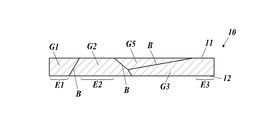
- FIG. 2 is a vertical cross-sectional view showing the insulating substrate of FIG.
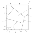
- FIG. 3 is a plan view showing the insulating substrate of FIG.
- the insulating substrate 10 is a SiC polycrystalline substrate in which a plurality of bulk crystallites are bonded while crystal growth occurs, and includes a plurality of bulk crystallites G1 to G7.
- the bulk crystallite means a mass of a single crystal grown in a three-dimensional direction.
- No grain boundary phase (for example, a phase containing a sintering aid used for firing a SiC multi-particle sintered substrate) is contained between adjacent bulk crystallites, and a grain boundary B as a boundary surface is interposed. It may be configured to be used.
- the phase means a structure having a thickness even if it is minute.
- the number of bulk crystallites G1 to G7 contained in the first surface 11 of the insulating substrate 10 may be 2 pieces / cm 2 or more and 100 pieces / cm 2 or less.
- thermal conductivity equivalent to that of a SiC single crystal substrate can be obtained.
- the number density of bulk crystallites is increased from 100 pieces / cm 2 , the thermal conductivity is lowered as compared with the SiC single crystal substrate.
- the number density of bulk crystallites is less than 2 pieces / cm 2 , the number of micropipes generated from the grain boundaries increases due to crystal mismatch, and the number of micropipes that penetrate from the first surface 11 to the second surface 12 It will increase.
- the size of the bulk crystallites G1 to G7 contained in the first surface 11 of the insulating substrate 10 is a minimum width of 1 mm to 5 mm, and the number of bulk crystallites G1 to G7 contained in the first surface 11 is 2 pieces / cm. It may be 2 or more and 10 pieces / cm 2 or less.
- the insulating substrate 10 has a range E1 to E3 (FIG. 2) in which no grain boundary exists between the first surface 11 and the second surface 12, that is, a single bulk crystallite from the first surface 11 to the second surface 12 Includes the occupied range E1 to E3.
- the ranges E1, E2, and E3 where the grain boundaries B do not exist overlap with the range where the wiring conductor 20 is located. May be good. Further, in the plan perspective of the first surface 11, a configuration in which the grain boundary B does not exist at a position overlapping the wiring conductor 20 may be adopted. In the insulating substrate 10, the range in which two or more grain boundaries B are included between the first surface 11 and the second surface 12 when viewed from the direction perpendicular to the first surface 11 is 20% or less in terms of area ratio. There may be.
- FIG. 4 is an image of an electron micrograph of the surface of the insulating substrate. In the photograph of FIG. 4, the brightness is changed according to the polytype of the bulk crystallite.
- the wiring board 1 contains a plurality of SiC bulk crystals having different polytypes.
- the polymorphism refers to a type of polymorph having the same chemical composition but different atomic arrangement of crystals.
- the plurality of bulk crystallites may all belong to ⁇ -SiC.
- ⁇ -SiC means a bulk crystallite other than 3C type, and is a high-purity SiC crystal.
- ⁇ -SiC can be formed by growing crystals at 2000 ° C. or higher by a sublimation recrystallization method.
- the total bulk crystallites contained in the insulating substrate 10 include any of 4H type, 6H type, and 15R type bulk crystallites, and the volume ratio of the 4H type, 6H type, and 15R type bulk crystallites.
- the total may be 80% or more.
- the volume ratio of the 3C type bulk crystallites contained in the insulating substrate 10 may be 1% or less.
- the plurality of bulk crystallites may include those having different plane directions from each other.
- the plane direction means the orientation of a specific crystal plane.
- Bulk crystals of different polytypes contained in the insulating substrate 10 may have different plane directions from each other, and a plurality of bulk crystallites of the same polytype contained in the insulating substrate 10 may have different plane directions from each other. May have.
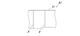
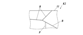
- FIG. 5A to 5C are views for explaining three types of SiC substrates
- FIG. 5A is a diagram showing a cut surface of a SiC single crystal substrate
- FIG. 5B is a diagram showing a cut surface of the SiC crystal substrate of the first embodiment
- FIG. 5C is a diagram showing a cut surface of a SiC multi-particle sintered substrate.
- the SiC substrate includes a SiC single crystal substrate K1 (FIG. 5A) grown into a single crystal by the sublimation recrystallization method and a SiC polycrystal substrate K2 (FIG. 5A) in which a plurality of bulk sinters are grown and bonded by the sublimation recrystallization method.
- a SiC single crystal substrate K1 (FIG. 5A) grown into a single crystal by the sublimation recrystallization method
- a SiC polycrystal substrate K2 FIG. 5A
- There are types such as FIG. 5B) and a SiC multi-particle sintered substrate K3 (FIG. 5C) in which SiC crystals are crushed onto fine particles and then sintered by firing.
- the SiC single crystal substrate K1 Since the SiC single crystal substrate K1 is a single crystal, it has high thermal conductivity.
- the SiC single crystal substrate K1 has anisotropy of the coefficient of thermal expansion, and often contains a micropipe P formed by a series of crystal defects in the crystal growth process.
- the micropipe P is often continuous from the first surface 11 of the SiC single crystal substrate K1 to the surface opposite to the first surface 11.
- the SiC single crystal substrate K1 has a high production margin ratio because the single crystal portion is extracted, and further, the production cost is high because a seed crystal is required.
- the SiC polycrystalline substrate K2 can be obtained by growing a SiC crystal by a physical vapor phase growth method such as a sublimation recrystallization method without using a seed crystal substrate or using a substrate having a plurality of seed crystals. ..
- a physical vapor phase growth method such as a sublimation recrystallization method without using a seed crystal substrate or using a substrate having a plurality of seed crystals. ..
- a physical vapor phase growth method such as a sublimation recrystallization method without using a seed crystal substrate or using a substrate having a plurality of seed crystals. ..
- adjacent bulk crystallites come into contact with each other to form bonded grain boundaries B. Since the SiC polycrystalline substrate K2 contains a plurality of bulk crystallites having different growth directions (that is, plane directions), grain boundaries B having irregular orientations are included.
- the SiC polycrystalline substrate K2 has a plurality of micros having different extending directions (directions of the central axis). Including pipes. Further, since the grain boundary B is generated by abutting adjacent bulk crystallites in the growth process, when the bulk crystallites include a micropipe, the end portion of the micropipe may be blocked by the adjacent bulk crystallites. is there. That is, in the process of crystal growth, a micropipe P whose end is blocked by adjacent bulk crystallites may be generated.
- the SiC polycrystalline substrate K2 does not need to extract a single crystal portion, it can be manufactured at a lower cost than the SiC single crystal substrate K1.
- the insulating substrate 10 of the first embodiment is obtained by cutting the SiC polycrystalline substrate K2 to a predetermined size.
- the SiC multi-particle sintered substrate K3 is configured such that particles are collected via a sintering aid such as a binder before firing, and the particles are sintered via the sintering aid.
- the sintering aid is a liquid phase, such as alumina.
- the SiC multi-particle sintered substrate K3 contains a large number of fine grain boundaries BL and the remaining sintering aid J.
- the grain boundary BL of the SiC multi-particle sintered substrate K3 includes those having a layered thickness.
- the SiC multi-particle sintered substrate K3 has low thermal conductivity because thermal vibration is diffused or absorbed by many grain boundaries BL and the sintering aid J.
- the SiC multi-particle sintered substrate K3 does not include a crystal growth step in the manufacturing process.
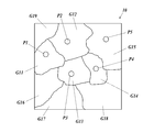
- FIG. 6A is a plan view showing an example of a micropipe included in the insulating substrate of the first embodiment.
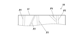
- FIG. 6B is a side view showing an example of the micropipe included in the insulating substrate of the first embodiment.
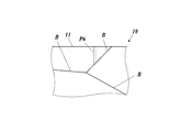
- FIG. 7 is a side view showing an example of the micropipe included in the insulating substrate of the first embodiment. 6A, 6B and 7 show an individual different from the insulating substrate 10 shown in FIGS. 2 and 3.
- the insulating substrate 10 of the first embodiment is obtained by cutting the SiC polycrystalline substrate K2 as described above. Therefore, as shown in FIGS. 6A and 6B, a plurality of bulk crystallites G11 to G19 having different plane directions may be included, and a plurality of micropipes P1 to P5 having different orientations may be included.
- the micropipes P1 to P5 having the first end opened on the first surface 11 have a central axis inclined at various angles with respect to the first surface 11. Further, as shown in FIG. 7, a micropipe P6 having a first end opened on the first surface 11 and a second end blocked by a grain boundary B may be included.
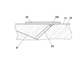
- FIG. 8 is a diagram illustrating the operation of the micropipe included in the insulating substrate of the first embodiment.
- the wiring conductor 20 is formed in the opening of the micropipe P4, a part of the wiring conductor 20 extends in the micropipe P4. Then, the extending portion 20k extending diagonally exerts an anchor effect, and the film of the wiring conductor 20 can be made difficult to peel off. Further, the wiring conductor 20 is formed in a range in which the plurality of micropipes P1 to P5 are opened, and extends to the ends of the plurality of micropipes P1 to P5, so that extending portions having different angles can be obtained. , The film of the wiring conductor 20 can be made difficult to peel off.
- the micropipe P4 opened in the first surface 11 is blocked by other bulk crystallites via the grain boundary B on the way and does not reach the second surface 12. There are many. Therefore, high insulation between the first surface 11 and the second surface 12 can be ensured.
- the insulating substrate 10 may have a resistivity of 1 ⁇ 10 3 ⁇ ⁇ cm or more. Further, the nitrogen content in the insulating substrate 10 may be 3 ⁇ 10 17 atoms / cm 3 (atomic number density) or less. Further, the insulating substrate 10 may have a resistivity of 1 ⁇ 10 5 ⁇ ⁇ cm or more. The vanadium content in the insulating substrate 10 may be 1 ⁇ 10 15 atoms / cm 3 or more and 1 ⁇ 10 18 atoms / cm 3 or less.
- the SiC substrate As described above, by lowering the amount of nitrogen as a dopant in the SiC substrate and increasing the content of vanadium that captures free electrons, it is possible to increase the low efficiency of the insulating substrate 10 and obtain high insulating properties of the insulating substrate 10. it can. Further, by setting the content of vanadium to the above content or less, the number of micropipes can be reduced, the scattering action of thermal vibration can be suppressed, and the high thermal conductivity of the insulating substrate 10 can be maintained.
- the wiring board 1 of the first embodiment a plurality of bulk crystallites G1 to G7 and G11 to G19 of SiC having different polytypes are included. Therefore, the manufacturing cost can be reduced by not using the single crystal substrate, and the insulating substrate 10 contains SiC bulk crystals G1 to G7 and G11 to G19, so that the wiring board 1 has high thermal conductivity. Performance can be obtained. Further, the number of bulk crystallites G1 to G7 and G11 to G19 per unit area on the first surface 11 of the above-mentioned bulk crystallites, the range E1 to E3 (FIG. 2) in which the grain boundary B does not exist, the range E1 to E3 and the wiring conductor 20 Higher heat conduction performance can be obtained by adopting the arrangement relation of the above or a plurality of the above.
- the insulating board 10 includes a plurality of bulk crystallites G1 to G7 and G11 to G19 having different plane directions. Therefore, the anisotropy of thermal expansion is alleviated, the total amount of thermal deformation of the insulating substrate 10 is reduced, and the distortion of the electronic component 50 and the stress between the electronic component 50 can be reduced. Further, the stress caused by the thermal expansion difference between the insulating substrate 10 and the wiring conductor 20 or the stress caused by the thermal expansion difference between the wiring board 1 and the electronic component 50 becomes isotropic, and the harmful effects caused by the stress are caused. It can be made less likely to occur. In addition, the insulating substrate 10 is dispersed in the plane direction, so that it is possible to obtain isotropic characteristics in terms of thermal conductivity.
- the SiC crystal of the insulating substrate 10 has the ratio of the polytype as described above, higher thermal conductivity can be realized.
- the film of the wiring conductor 20 can be made more difficult to peel off due to the characteristics of the micropipes P1 to P6 described above, and the insulating property is lowered by the micropipes P1 to P6. It is possible to make it difficult for the action to occur. Further, the high efficiency of the insulating substrate 10 itself can be realized by the content of the above-mentioned components of the insulating substrate 10. Therefore, the reliability of the wiring conductor 20 of the wiring board 1 and the insulation property of the insulating substrate 10 can be improved.
- the electronic device 60 As shown in FIG. 1, the electronic device 60 according to the first embodiment is configured by mounting an electronic component 50 on a wiring board 1.
- the electrodes of the electronic component 50 are electrically connected to the wiring conductor 20.
- the electrodes of the electronic component 50 may be directly bonded to the wiring conductor 20, or may be connected via a bonding member such as a bonding wire.
- the electronic device 60 may include a package that houses the wiring board 1 and the electronic component 50.
- Examples of the electronic component 50 include optical elements such as LD (LaserDiode), PD (PhotoDeode), LED (LightEmittingDiode), and imaging elements such as CCD (ChargeCoupledDevice) type and CMOS (ComplementaryMetalOxideSemiconductor) type.
- Various electronic components such as piezoelectric vibrators such as crystal transducers, elastic surface wave elements, semiconductor elements such as semiconductor integrated circuit elements (ICs), electrostatic capacity elements, inductor elements and resistors can be applied.
- the electronic module 100 is configured by mounting an electronic device 60 on a module substrate 110.
- other electronic devices, electronic elements, electric elements, and the like may be mounted on the module substrate 110.
- the module substrate 110 is provided with an electrode 111, and the electronic device 60 may be bonded to the electrode 111 via a bonding material 113 such as solder or gold tin.
- the wiring conductor of the package may be joined to the electrode 111 of the module substrate 110.
- the high heat dissipation characteristics and the good electrical characteristics of the electronic component 50 can be obtained, so that the reliability can be improved.
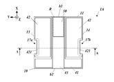
- FIG. 9A is a plan view showing a wiring board, an electronic device, and an electronic module according to the second embodiment of the present disclosure.
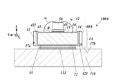
- 9B is a vertical cross-sectional view taken along the line AA of FIG. 9A.
- the X direction of FIGS. 9A and 9B will be described as forward, the Y direction will be described as left, and the Z direction will be described as upward.
- the direction shown in the second embodiment may be different from the direction when the wiring board is used.
- the wiring board 1A is a submount on which electronic components (light emitting elements) 50 such as LDs, PDs, and LEDs are mounted.
- the submount is interposed between the electronic component 50 and the package or between the electronic component 50 and the module substrate 110, conducts the heat of the electronic component 50 and releases it to the package or the module substrate 110, and further, the electronic component.
- It is a wiring board through which a drive current flows through 50.
- the wiring board 1A includes an insulating substrate 10 having a first surface 11, a second surface 12 opposite to the first surface 11, a first side surface 13, and a second side surface 14 opposite to the first side surface 13. Be prepared.
- the first surface 11 corresponds to the upper surface
- the second surface 12 corresponds to the lower surface
- the first side surface corresponds to the left side surface
- the second side surface corresponds to the right side surface.
- the insulating substrate 10 has casting grooves 17a and 17b located on the first side surface 13 and the second side surface 14. The groove portions 17a and 17b are located from the first surface 11 to the second surface 12.
- the first surface 11 includes a mounting portion R of the electronic component 50.
- the first surface 11 has a front end (first end) b1 and a rear end (second end) b2 facing the front end b1 in a plan view.
- the mounting portion R is located closer to the front end b1 than to the rear end b2.
- the mounting portion R may be in contact with the front end b1.
- the mounting portion R may be located at the center of the first surface 11 in the left-right direction.
- the maximum heat generating portion of the electronic component 50 may be located at the front portion of the mounting portion R.
- the groove portions 17a and 17b of the casting are located closer to the rear end b2 than the front end b1 of the first surface 11.
- the groove portions 17a and 17b may be located closer to the rear end than the front end of the insulating substrate 10 in the entire area in the thickness direction.
- the wiring board 1A further includes a wiring conductor 41 located on the first surface 11, a wiring conductor 42 located on the first surface 11, the second surface 12, the first side surface 13 and the second side surface 14, and the first surface 11. It has a joining conductor 43 located on the wiring conductor 41 of the above, and a joining conductor 44 located on the wiring conductor 42 of the second surface 12. On the first side surface 13 and the second side surface 14, the wiring conductor 42 is located in the groove portions 17a and 17b of the casting.
- the wiring conductors 41 and 42 may be film-like conductors, and further, an adhesion layer containing Ti (titanium) or the like, a barrier layer containing Pt (platinum) or the like, and a conductor layer containing Au (gold) or the like are formed. It may be a laminated conductor.
- the wiring conductor 42 located on the first surface 11 corresponds to an example of the first wiring according to the present disclosure
- the wiring conductor 42 located on the second surface 12 corresponds to an example of the second wiring according to the present disclosure.
- the wiring conductor 42 (conductor film 421) located in the grooves 17a and 17b corresponds to an example of the third wiring according to the present disclosure.
- the wiring conductor 41 is located in a region overlapping the mounting portion R of the first surface 11.
- the wiring conductor 41 may extend from the vicinity of the front end to the vicinity of the rear end of the first surface 11, or extends from the vicinity of the left end to the vicinity of the right end in the vicinity of the rear end of the first surface 11, and is inverted T when viewed from above. It may be in the shape of a letter.
- the wiring conductor 42 is separated from the wiring conductor 41 on the first surface 11.
- the wiring conductor 42 is located on the first surface 11 and the second surface 12 as a conductor film.
- the wiring conductor 42 further includes a conductor film 421 located in the grooves 17a and 17b, which is thicker than the conductor film located on the first surface 11 and the second surface 12.
- the conductor film 421 can be thickened by plating a conductor such as Au on the conductor films of the grooves 17a and 17b formed together with the conductor films of the first surface 11 and the second surface 12.
- the bonding conductors 43 and 44 may have a structure in which a barrier layer containing Pt or the like and a conductor layer such as AuSn (gold tin) are laminated.
- the bonding conductor 43 on the upper surface is located at the mounting portion R on the wiring conductor 41, and the electronic component 50 is bonded.
- the joining conductor 43 may extend beyond the mounting portion R from the front end b1 to the rear end b2 of the first surface 11.
- the lower surface bonding conductor 44 is located on the wiring conductor 42 (so as to contact the lower surface of the wiring conductor 42) and is bonded to the electrode 111 of the package or module substrate 110.
- the maximum width (for example, front-rear width) of the insulating substrate 10 in the plane direction along the first surface 11 is larger than the average thickness in the direction perpendicular to the first surface 11 (thickness direction).
- first surface 11 is rectangle close to a square or square area 0.01 cm 2 ⁇ 1.00 cm 2, a thickness of 0.1 mm ⁇ 0.8 mm.
- FIG. 10 is a diagram showing the first surface of the insulating substrate according to the second embodiment.
- the insulating substrate 10 is a substrate obtained by cutting a polycrystalline SiC substrate to a predetermined size, and includes a plurality of bulk crystallites G21 to G25 as shown in FIG.
- the bulk crystallite means a mass of a single crystal grown in a three-dimensional direction.
- the grain boundary phase (for example, the phase containing the sintering aid of the ceramic substrate) is not contained between the adjacent bulk crystallites G21 to G25, and the grain boundary B as the boundary surface exists.
- the insulating substrate 10 may contain a plurality of SiC bulk crystals having different polytypes.
- the polymorphism refers to a type of polymorph having the same chemical composition but different atomic arrangement of crystals.
- the plurality of bulk crystallites may all belong to ⁇ -SiC.
- ⁇ -SiC means a bulk crystallite other than 3C type, and is a high-purity SiC crystal.
- ⁇ -SiC can be formed by growing crystals at 2000 ° C. or higher by a sublimation recrystallization method.
- the total bulk crystallites contained in the insulating substrate 10 include any of 4H type, 6H type, and 15R type bulk crystallites, and the volume ratio of the 4H type, 6H type, and 15R type bulk crystallites.
- the total may be 80% or more.
- the volume ratio of the 3C type bulk crystallites contained in the insulating substrate 10 may be 1% or less.
- the plane directions of the plurality of bulk crystallites G21 to G25 may be different from each other.
- the plane direction means the orientation of a specific crystal plane.
- Bulk crystals of different polytypes contained in the insulating substrate 10 may have different plane directions from each other, and a plurality of bulk crystallites of the same polytype contained in the insulating substrate 10 may have different plane directions from each other. May have.
- the thermal conductivity in the plane direction (X direction and Y direction) along the first surface 11 is higher than the thermal conductivity in the thickness direction (Z direction).
- the thermal conductivity in a specific direction is obtained by cutting the insulating substrate 10 into, for example, a cube, and measuring the thermal conductivity in the specific direction by a laser flash method.
- the number of grain boundaries B per unit length in the plane direction along the first surface 11 is smaller than the number of grain boundaries B per unit length in the thickness direction. Further, the insulating substrate 10 has 0 to 3 grain boundaries B in the plane direction (for example, the number of grain boundaries B from the front end to the rear end of the insulating substrate 10). As shown by the alternate long and short dash line in FIG. 10, the number of grain boundaries B in a specific direction is determined by counting the intersection N of the virtual straight line L extending in the specific direction and the grain boundaries B on the surface or cross section of the insulating substrate 10. It can be obtained based on the counted value. The number of grain boundaries B is a value obtained by counting the number of intersections N with the grain boundaries B for five or more virtual straight lines L randomly distributed in the insulating substrate 10 in a specific direction and averaging the counted values. Is defined as.
- the polycrystalline SiC substrate which is the material of the insulating substrate 10 can be manufactured in the same manner as the SiC polycrystalline substrate K2 of the first embodiment.
- the insulating substrate 10 is obtained by cutting a polycrystalline SiC substrate into a predetermined size. The cutting location and cutting direction are determined so as to satisfy the number of grain boundaries.
- the electronic device 60A As shown in FIG. 9B, the electronic device 60A according to the second embodiment is configured by mounting an electronic component 50 which is a light emitting element on a wiring board 1A. One electrode of the electronic component 50 is joined to the joining conductor 43 on the wiring conductor 41. Another electrode of the electronic component 50 is connected to the wiring conductor 42 on the first surface 11 via a bonding member such as a bonding wire w.
- a bonding member such as a bonding wire w.
- the electronic module 100A is configured by mounting the electronic device 60A on the module substrate 110.
- other electronic devices, electronic elements, electric elements, and the like may be mounted on the module substrate 110.
- An electrode 111 may be provided on the module substrate 110, and the electronic device 60A may be bonded to the electrode 111 via a bonding conductor 44.
- the wiring conductor of the package may be joined to the electrode 111 of the module substrate 110.
- the casterment conductor film 421 has a smaller surface area, but is thicker, so that Joule heat can be concentrated in the wiring conductors 42. Therefore, the conductor film 421 of the casting can be made less likely to deteriorate.
- the electronic component 50 When the electronic component 50 is driven, the electronic component 50 generates heat. For example, the amount of heat generated increases at the front end of the electronic component 50 from which light is emitted.
- the heat generated from the electronic component 50 is transferred from the joining conductor 43 of the mounting portion R to the first surface 11 of the insulating substrate 10 via the wiring conductor 41, and then is a flat surface along the first surface 11 of the insulating substrate 10. It is transmitted to the second surface 12 side ( ⁇ Z direction) while spreading widely in the directions ( ⁇ X direction and ⁇ Y direction).
- the heat spreads widely in the plane direction because the thermal conductivity in the X direction and the Y direction is higher than the thermal conductivity in the Z direction of the insulating substrate 10.
- the heat transmitted through the insulating substrate 10 is uniformly spread over the entire area of the second surface 12 and is transmitted to the module substrate 110 via the wiring conductor 42 and the bonding conductor 44. Since the insulating substrate 10 is composed of a polycrystalline SiC substrate, it has a high thermal conductivity even in the Z direction, and efficiently releases the heat of the electronic component 50 by the high heat dissipation action in addition to the above-mentioned heat conduction mode. it can.
- the insulating substrate 10 on which the wiring conductors 41 and 42 are located is a polycrystalline SiC substrate, and is formed on the first surface 11 having the mounting portion R of the electronic component 50.
- the maximum width in the plane direction (XY directions) along the line is larger than the average thickness in the Z direction perpendicular to the first surface 11.
- the insulating substrate 10 has a higher thermal conductivity in the plane direction than the thermal conductivity in the thickness direction. Therefore, as described above, the heat of the electronic component 50 mounted on the mounting portion R can be efficiently released with a high heat dissipation effect. Further, since the polycrystalline SiC substrate can reduce the manufacturing cost as compared with the single crystal SiC substrate, the wiring substrate 1A can be manufactured at a low cost.
- the number of grain boundaries B per unit length in the plane direction of the insulating substrate 10 is smaller than the number of grain boundaries B per unit length in the thickness direction.
- the grain boundary B has an action of lowering the thermal conductivity.
- the number of grain boundaries B in the plane direction of the insulating substrate 10 is 0 to 3. By setting the number to this number, it is possible to realize the wiring board 1A having high heat dissipation while maintaining the low manufacturing cost of the insulating substrate 10.
- the mounting portion R of the electronic component 50 is located closer to the front end b1 than the rear end b2 of the first surface 11
- the casting (grooves 17a, 17b and the conductor film) 421) is located closer to the rear end b2 than the front end b1 of the first surface 11. Since the heat of the electronic component 50 is transmitted in the thickness direction while spreading in the plane direction on the insulating substrate 10, the larger the volume of the insulating substrate 10 in the vicinity of the heat generating portion, the better the heat dissipation.
- the casting has the effect of reducing the volume of the insulating substrate 10 by the grooves 17a and 17b, but the above arrangement allows the portion for reducing the volume of the insulating substrate 10 to be separated from the mounting portion R. Therefore, it is difficult to reduce the heat dissipation of the wiring board 1A by reducing the volume of the insulating substrate 10 due to casting.
- the conductor film 421 of the casting is thicker than the wiring conductors 41 and 42 on the first surface 11 and the wiring conductor 42 on the second surface 12. Therefore, when the current is concentrated on the conductor film 421 of the casting, the Joule heat of the conductor film 421 can be reduced and the conductor film 421 can be less likely to deteriorate.
- the high heat dissipation characteristics of the electronic component 50 can be obtained, so that the reliability can be improved.
- the wiring board, the electronic device, and the electronic module of the present disclosure are not limited to the above-described embodiment.
- the first embodiment shows an example of a method for manufacturing an insulated substrate for a wiring board, another manufacturing method capable of manufacturing a similar insulated substrate may be adopted.
- the wiring board is applied as a submount on which one electronic component is mounted, but it may be applied as a wiring board on which a plurality of electronic components are mounted.
- the types and arrangements of the wiring conductors shown in the first embodiment are merely examples.
- the shape of the insulating substrate, the arrangement of the wiring conductors located on the insulating substrate, the pattern, the components, and the like can be appropriately changed.
- This disclosure can be used for wiring boards, electronic devices and electronic modules.
Landscapes
- Cooling Or The Like Of Semiconductors Or Solid State Devices (AREA)
- Chemical & Material Sciences (AREA)
- Crystallography & Structural Chemistry (AREA)
- Structure Of Printed Boards (AREA)
Abstract
Description
第1面を有する絶縁基板と、
該絶縁基板に位置する配線導体とを備え、
前記絶縁基板はポリタイプが異なるSiCのバルク結晶子を複数含む、
上記の配線基板と、
前記配線基板に搭載された電子部品と、
を備える。
上記の電子装置と、
前記電子装置が搭載されたモジュール用基板と、
を備える。
図1は、本開示の実施形態1に係る配線基板を有する電子装置及び電子モジュールを示す図である。実施形態1に係る配線基板1は、第1面11を有する板状体である絶縁基板10と、絶縁基板10の第1面11に位置する配線導体20とを備える。配線基板1は、第1面11の反対側に第2面12を有する。第1面11及び第2面12は、板状体の広い方の2面であってもよく、電子部品が搭載される面であってもよい。配線導体20は、Ti(チタン)、Cr(クロム)又はTi、Crの両方等を主成分とする密着層21と、Pt(白金)等を主成分とするバリア層22と、Au(金)等を主成分とする導体層23と、電子部品50を接合するAuSn(金スズ)等の接合導体25とが積層されて構成されてもよい。
図5A~図5Cは、三種類のSiC基板を説明する図であり、図5AはSiC単結晶基板の切断面を示す図、図5Bは実施形態1のSiC結晶基板の切断面を示す図、図5CはSiC多粒子焼結基板の切断面を示す図である。
図6Aは、実施形態1の絶縁基板に含まれるマイクロパイプの一例を示す平面図である。図6Bは実施形態1の絶縁基板に含まれるマイクロパイプの一例を示す側面図である。図7は、実施形態1の絶縁基板に含まれるマイクロパイプの一例を示す側面図である。図6A、図6B及び図7には、図2及び図3に示した絶縁基板10とは別の個体を示している。
絶縁基板10は、1×10³ Ω・cm以上の抵抗率を有してもよい。さらに、絶縁基板10における窒素の含有量は、3×10¹⁷ atoms/cm3(原子数密度)以下であってもよい。また、絶縁基板10は、1×105 Ω・cm以上の抵抗率を有してもよい。また、絶縁基板10におけるバナジウムの含有量は、1×10¹⁵ atoms/cm3以上1×1018 atoms/cm3以下であってもよい。
実施形態1に係る電子装置60は、図1に示すように、配線基板1に電子部品50が搭載されて構成される。電子部品50の電極は、配線導体20に電気的に接続される。電子部品50の電極は、配線導体20に直接接合されてもよいし、ボンディングワイヤー等の接合部材を介して接続されてもよい。電子装置60は、配線基板1と電子部品50とを収容するパッケージを含んでもよい。
図9Aは、本開示の実施形態2に係る配線基板、電子装置及び電子モジュールを示す平面図である。図9Bは、図9AのA-A線における縦断面図である。以下の説明では、図9A及び図9BのX方向を前方、Y方向を左方、Z方向を上方として説明する。実施形態2で示す方向は、配線基板の使用時の方向と異なっていてもよい。
絶縁基板10の材料である多結晶SiC基板は、実施形態1のSiC多結晶基板K2と同様に製造できる。絶縁基板10は、多結晶SiC基板を、所定サイズに切断して得られる。切断箇所及び切断の向きは、粒界の個数条件を満たすように決定される。
実施形態2に係る電子装置60Aは、図9Bに示すように、配線基板1Aに発光素子である電子部品50が搭載されて構成される。電子部品50の一つの電極は、配線導体41上の接合用導体43に接合される。電子部品50のもう一つの電極は、ボンディングワイヤーw等の接合部材を介して第1面11上の配線導体42に接続される。
10 絶縁基板
11 第1面
12 第2面
20 配線導体
50 電子部品
60、60A 電子装置
100、100A 電子モジュール
110 モジュール用基板
B 粒界
G1~G7、G11~G19、G21~G25 バルク結晶子
P、P1~P6 マイクロパイプ
b1 前端
b2 後端
R 搭載部
13 第1側面
14 第2側面
17a、17b 溝部
41 配線導体
42 配線導体(第1配線、第2配線、第3配線)
43、44 接合用導体
421 導体膜(第3配線)
Claims (20)
- 第1面を有する絶縁基板と、
該絶縁基板に位置する配線導体とを備え、
前記絶縁基板はポリタイプが異なるSiCのバルク結晶子を複数含む、
配線基板。 - 前記第1面における前記バルク結晶子の個数が、2個/cm2以上100個/cm2以下である、
請求項1に記載の配線基板。 - 前記絶縁基板は、4H型バルク結晶子、6H型バルク結晶子及び15R型バルク結晶子の少なくともいずれかを含み、
前記4H型バルク結晶子、前記6H型バルク結晶子及び前記15R型バルク結晶子の体積比の合計が、80%以上である、
請求項1又は請求項2に記載の配線基板。 - 3C型のバルク結晶子の体積比が1%以下である、
請求項1から請求項3のいずれか一項に記載の配線基板。 - 複数の前記バルク結晶子は、互いに面方向が異なるものを含む、
請求項1から請求項4のいずれか一項に記載の配線基板。 - 前記絶縁基板は、第1方向に延びるマイクロパイプを有する第1のバルク結晶子と、前記第1方向とは異なる第2方向に延びるマイクロパイプを有する第2のバルク結晶子とを含む、
請求項1から請求項5のいずれか一項に記載の配線基板。 - 前記絶縁基板は、隣り合う第3のバルク結晶子と第4のバルク結晶子とを含み、
前記第3のバルク結晶子は、前記第4のバルク結晶子に端部が遮られたマイクロパイプを有する、
請求項1から請求項6のいずれか一項に記載の配線基板。 - 前記絶縁基板は、前記第1面の反対側に第2面を有し、
前記絶縁基板は、前記第1面から前記第2面まで粒界が存在しない部位を含む、
請求項1から請求項7のいずれか一項に記載の配線基板。 - 前記配線導体は、前記第1面に位置しており、
前記第1面の平面透視において、前記粒界が存在しない部位が、前記配線導体と重なる、
請求項8記載の配線基板。 - 前記絶縁基板が1×10³Ω・cm以上の抵抗率を有する、
請求項1から請求項9のいずれか一項に記載の配線基板。 - 前記絶縁基板の窒素の含有量が、1×10¹⁷atoms/cm3以下である、
請求項10に記載の配線基板。 - 前記絶縁基板が1×10⁵Ω・cm以上の抵抗率を有する、
請求項1から請求項11のいずれか一項に記載の配線基板。 - 前記絶縁基板のバナジウムの含有量が、1×10¹⁵atoms/cm3以上1×1018atoms/cm3以下である、
請求項12に記載の配線基板。 - 隣り合う前記バルク結晶子の間に粒界の相を有していない、
請求項1から請求項13のいずれか一項に記載の配線基板。 - 前記絶縁基板に位置する前記配線導体を備えたサブマウントであり、
前記第1面は発光素子である電子部品を搭載する搭載部を含み、
前記絶縁基板は、前記第1面に沿った平面方向の最大幅よりも厚み方向の平均厚みが小さく、かつ、前記平面方向の熱伝導率が前記厚み方向の熱伝導率よりも高い、
請求項1記載の配線基板。 - 前記絶縁基板の前記平面方向における単位長さ当たりの粒界の個数が、前記絶縁基板の前記厚み方向における単位長さ当たりの粒界の個数よりも少ない、
請求項15記載の配線基板。 - 前記絶縁基板の前記平面方向における粒界の個数が0個~3個である、
請求項15又は請求項16記載の配線基板。 - 前記絶縁基板は、前記厚み方向に延在する溝部と、前記第1面とは反対の第2面とを有し、
前記配線導体は、前記第1面に位置する第1配線と、前記第2面に位置する第2配線と、前記溝部に位置し前記第1配線と前記第2配線とに接続される第3配線とを含み、
前記第1面は、平面視において第1端と、該第1端に対向する第2端とを有し、
前記搭載部は、前記第2端よりも前記第1端の近くに位置し、
前記溝部は、前記第1端よりも前記第2端の近くに位置する、
請求項15から請求項17のいずれか一項に記載の配線基板。 - 請求項1から請求項18のいずれか一項に記載の配線基板と、
前記配線基板に搭載された電子部品と、
を備える電子装置。 - 請求項19記載の電子装置と、
前記電子装置が搭載されたモジュール用基板と、
を備える電子モジュール。
Priority Applications (4)
| Application Number | Priority Date | Filing Date | Title |
|---|---|---|---|
| EP20881405.3A EP4053893A4 (en) | 2019-10-31 | 2020-10-30 | Wiring board, electronic device, and electronic module |
| CN202080075168.2A CN114600235A (zh) | 2019-10-31 | 2020-10-30 | 布线基板、电子装置以及电子模块 |
| JP2021553713A JP7263537B2 (ja) | 2019-10-31 | 2020-10-30 | 配線基板、電子装置及び電子モジュール |
| US17/771,042 US12500083B2 (en) | 2019-10-31 | 2020-10-30 | Wiring substrate, electronic device, and electronic module |
Applications Claiming Priority (4)
| Application Number | Priority Date | Filing Date | Title |
|---|---|---|---|
| JP2019198472 | 2019-10-31 | ||
| JP2019-198472 | 2019-10-31 | ||
| JP2020-059294 | 2020-03-30 | ||
| JP2020059294 | 2020-03-30 |
Publications (1)
| Publication Number | Publication Date |
|---|---|
| WO2021085587A1 true WO2021085587A1 (ja) | 2021-05-06 |
Family
ID=75715494
Family Applications (1)
| Application Number | Title | Priority Date | Filing Date |
|---|---|---|---|
| PCT/JP2020/040774 Ceased WO2021085587A1 (ja) | 2019-10-31 | 2020-10-30 | 配線基板、電子装置及び電子モジュール |
Country Status (5)
| Country | Link |
|---|---|
| US (1) | US12500083B2 (ja) |
| EP (1) | EP4053893A4 (ja) |
| JP (1) | JP7263537B2 (ja) |
| CN (1) | CN114600235A (ja) |
| WO (1) | WO2021085587A1 (ja) |
Cited By (1)
| Publication number | Priority date | Publication date | Assignee | Title |
|---|---|---|---|---|
| WO2026164293A1 (ja) * | 2025-01-30 | 2026-08-06 | 京セラ株式会社 | 電子部品搭載用基板および発光装置 |
Citations (4)
| Publication number | Priority date | Publication date | Assignee | Title |
|---|---|---|---|---|
| JP2004289011A (ja) * | 2003-03-24 | 2004-10-14 | Sumitomo Electric Ind Ltd | 発光モジュール |
| JP2007269627A (ja) * | 2002-03-19 | 2007-10-18 | Central Res Inst Of Electric Power Ind | 基板から継続するマイクロパイプを低減させるSiC結晶の製造方法およびSiC結晶、SiC単結晶膜、SiC半導体素子、SiC単結晶基板および電子デバイス、ならびにSiCバルク結晶の製造方法 |
| WO2016017319A1 (ja) * | 2014-07-28 | 2016-02-04 | 昭和電工株式会社 | SiCエピタキシャルウェハの製造方法、SiCエピタキシャルウェハ |
| JP2019062212A (ja) | 2013-04-27 | 2019-04-18 | 日亜化学工業株式会社 | 半導体レーザ装置 |
Family Cites Families (31)
| Publication number | Priority date | Publication date | Assignee | Title |
|---|---|---|---|---|
| US4701427A (en) | 1985-10-17 | 1987-10-20 | Stemcor Corporation | Sintered silicon carbide ceramic body of high electrical resistivity |
| JP3461274B2 (ja) * | 1996-10-16 | 2003-10-27 | 株式会社東芝 | 半導体装置 |
| US6497763B2 (en) * | 2001-01-19 | 2002-12-24 | The United States Of America As Represented By The Secretary Of The Navy | Electronic device with composite substrate |
| US6794684B2 (en) * | 2001-02-01 | 2004-09-21 | Cree, Inc. | Reflective ohmic contacts for silicon carbide including a layer consisting essentially of nickel, methods of fabricating same, and light emitting devices including the same |
| EP1306890A2 (en) * | 2001-10-25 | 2003-05-02 | Matsushita Electric Industrial Co., Ltd. | Semiconductor substrate and device comprising SiC and method for fabricating the same |
| EP1782454A4 (en) * | 2004-07-07 | 2009-04-29 | Ii Vi Inc | LITTLE DOPED SEMI-INSULATING SIC CRYSTALS AND METHODS |
| US7326971B2 (en) * | 2005-06-08 | 2008-02-05 | Cree, Inc. | Gallium nitride based high-electron mobility devices |
| US9388509B2 (en) * | 2005-12-07 | 2016-07-12 | Ii-Vi Incorporated | Method for synthesizing ultrahigh-purity silicon carbide |
| US7449065B1 (en) * | 2006-12-02 | 2008-11-11 | Ohio Aerospace Institute | Method for the growth of large low-defect single crystals |
| EP3848970A1 (en) * | 2007-01-22 | 2021-07-14 | Cree, Inc. | Multiple light emitting diode emitter |
| CN104364428B (zh) * | 2012-05-24 | 2017-09-05 | Ⅱ-Ⅵ公司 | 钒补偿的NU型和PI型SI SiC单晶及其晶体生长方法 |
| JP2014127678A (ja) * | 2012-12-27 | 2014-07-07 | Kyocera Corp | 配線基板および電子装置 |
| US9322110B2 (en) * | 2013-02-21 | 2016-04-26 | Ii-Vi Incorporated | Vanadium doped SiC single crystals and method thereof |
| US11721547B2 (en) * | 2013-03-14 | 2023-08-08 | Infineon Technologies Ag | Method for manufacturing a silicon carbide substrate for an electrical silicon carbide device, a silicon carbide substrate and an electrical silicon carbide device |
| JP2015126024A (ja) * | 2013-12-25 | 2015-07-06 | 株式会社豊田自動織機 | 半導体基板および半導体基板の製造方法 |
| WO2016140946A1 (en) * | 2015-03-02 | 2016-09-09 | University Of Maryland, College Park | Plasmon-enhanced terahertz graphene-based photodetector and method of fabrication |
| DE102015111213B4 (de) * | 2015-07-10 | 2023-05-04 | Infineon Technologies Ag | Verfahren zum Verringern einer bipolaren Degradation bei einem SiC-Halbleiterbauelement und Halbleiterbauelement |
| CN109996908B (zh) * | 2016-11-28 | 2021-06-11 | 三菱电机株式会社 | 碳化硅半导体晶片、碳化硅半导体芯片及碳化硅半导体装置的制造方法 |
| KR102004035B1 (ko) * | 2017-05-26 | 2019-07-25 | 엘지전자 주식회사 | 탄소 발열체 |
| JP7135302B2 (ja) * | 2017-11-08 | 2022-09-13 | 富士電機株式会社 | 炭化シリコン半導体装置及びその製造方法 |
| JP7422479B2 (ja) * | 2017-12-22 | 2024-01-26 | 株式会社レゾナック | SiCインゴット及びSiCインゴットの製造方法 |
| EP3514128A1 (en) * | 2018-01-18 | 2019-07-24 | Heraeus GMSI LLC | Process for manufacturing a silicon carbide coated body |
| DE102018106967B3 (de) * | 2018-03-23 | 2019-05-23 | Infineon Technologies Ag | SILIZIUMCARBID HALBLEITERBAUELEMENT und Halbleiterdiode |
| DE212019000020U1 (de) * | 2018-04-27 | 2019-11-28 | Rohm Co., Ltd. | SiC-Halbleitervorrichtungen |
| EP3832698A4 (en) * | 2018-07-27 | 2021-07-28 | Nissan Motor Co., Ltd. | SEMICONDUCTOR COMPONENT AND MANUFACTURING METHOD FOR IT |
| WO2020032206A1 (ja) * | 2018-08-10 | 2020-02-13 | ローム株式会社 | SiC半導体装置 |
| JP6563093B1 (ja) * | 2018-08-10 | 2019-08-21 | ローム株式会社 | SiC半導体装置 |
| CN112567531A (zh) * | 2018-08-10 | 2021-03-26 | 罗姆股份有限公司 | SiC半导体装置 |
| US10825733B2 (en) * | 2018-10-25 | 2020-11-03 | United Silicon Carbide, Inc. | Reusable wide bandgap semiconductor substrate |
| US11967616B2 (en) * | 2018-12-07 | 2024-04-23 | Hitachi Energy Ltd | Vertical silicon carbide power MOSFET and IGBT and a method of manufacturing the same |
| US10611052B1 (en) * | 2019-05-17 | 2020-04-07 | Cree, Inc. | Silicon carbide wafers with relaxed positive bow and related methods |
-
2020
- 2020-10-30 US US17/771,042 patent/US12500083B2/en active Active
- 2020-10-30 WO PCT/JP2020/040774 patent/WO2021085587A1/ja not_active Ceased
- 2020-10-30 JP JP2021553713A patent/JP7263537B2/ja active Active
- 2020-10-30 EP EP20881405.3A patent/EP4053893A4/en active Pending
- 2020-10-30 CN CN202080075168.2A patent/CN114600235A/zh active Pending
Patent Citations (4)
| Publication number | Priority date | Publication date | Assignee | Title |
|---|---|---|---|---|
| JP2007269627A (ja) * | 2002-03-19 | 2007-10-18 | Central Res Inst Of Electric Power Ind | 基板から継続するマイクロパイプを低減させるSiC結晶の製造方法およびSiC結晶、SiC単結晶膜、SiC半導体素子、SiC単結晶基板および電子デバイス、ならびにSiCバルク結晶の製造方法 |
| JP2004289011A (ja) * | 2003-03-24 | 2004-10-14 | Sumitomo Electric Ind Ltd | 発光モジュール |
| JP2019062212A (ja) | 2013-04-27 | 2019-04-18 | 日亜化学工業株式会社 | 半導体レーザ装置 |
| WO2016017319A1 (ja) * | 2014-07-28 | 2016-02-04 | 昭和電工株式会社 | SiCエピタキシャルウェハの製造方法、SiCエピタキシャルウェハ |
Non-Patent Citations (1)
| Title |
|---|
| See also references of EP4053893A4 |
Cited By (1)
| Publication number | Priority date | Publication date | Assignee | Title |
|---|---|---|---|---|
| WO2026164293A1 (ja) * | 2025-01-30 | 2026-08-06 | 京セラ株式会社 | 電子部品搭載用基板および発光装置 |
Also Published As
| Publication number | Publication date |
|---|---|
| EP4053893A1 (en) | 2022-09-07 |
| US20220367183A1 (en) | 2022-11-17 |
| CN114600235A (zh) | 2022-06-07 |
| US12500083B2 (en) | 2025-12-16 |
| JP7263537B2 (ja) | 2023-04-24 |
| JPWO2021085587A1 (ja) | 2021-05-06 |
| EP4053893A4 (en) | 2023-11-15 |
Similar Documents
| Publication | Publication Date | Title |
|---|---|---|
| EP2214201B1 (en) | Process for producing substrate for power module, substrate for power module, and power module | |
| JP4045767B2 (ja) | 半導体発光装置 | |
| CN102593081B (zh) | 包括散热器的半导体器件 | |
| US8609993B2 (en) | Power module substrate, power module, and method for manufacturing power module substrate | |
| JPWO2004084319A1 (ja) | 発光素子搭載用部材およびそれを用いた半導体装置 | |
| WO2009034454A2 (en) | Semiconductor device | |
| EP2393110A1 (en) | Heat dissipating base body and electronic device using same | |
| WO2005020315A1 (ja) | 素子接合用基板、素子接合基板及びその製造方法 | |
| JP7263537B2 (ja) | 配線基板、電子装置及び電子モジュール | |
| KR20040014475A (ko) | 소자 접합용 기판 및 그 제조 방법 | |
| CN100428432C (zh) | 元件接合用基板及其制造方法 | |
| US20020112882A1 (en) | Ceramic circuit board | |
| JP4699822B2 (ja) | 半導体モジュ−ルの製造方法 | |
| JP3801108B2 (ja) | 半導体素子の固定方法および半導体装置 | |
| JP2000269392A (ja) | 半導体モジュール及び放熱用絶縁板 | |
| JP3840132B2 (ja) | ペルチェ素子搭載用配線基板 | |
| TWI683373B (zh) | 電子模組 | |
| JP7358525B2 (ja) | 電子素子搭載用基板、電子装置および電子モジュール | |
| JP5614127B2 (ja) | パワーモジュール用基板及びその製造方法 | |
| JP7237687B2 (ja) | 配線基板、電子装置及び電子モジュール | |
| JP5034723B2 (ja) | サージ吸収素子及び発光装置 | |
| JP4121827B2 (ja) | モジュール構造体の製造方法 | |
| JP2005223348A (ja) | 多層基板 | |
| US12224390B2 (en) | Electronic component mounting substrate and electronic device | |
| JP3808357B2 (ja) | 配線基板 |
Legal Events
| Date | Code | Title | Description |
|---|---|---|---|
| 121 | Ep: the epo has been informed by wipo that ep was designated in this application |
Ref document number: 20881405 Country of ref document: EP Kind code of ref document: A1 |
|
| ENP | Entry into the national phase |
Ref document number: 2021553713 Country of ref document: JP Kind code of ref document: A |
|
| NENP | Non-entry into the national phase |
Ref country code: DE |
|
| ENP | Entry into the national phase |
Ref document number: 2020881405 Country of ref document: EP Effective date: 20220531 |
|
| WWG | Wipo information: grant in national office |
Ref document number: 17771042 Country of ref document: US |