WO2021090527A1 - 多層配線基板 - Google Patents
多層配線基板 Download PDFInfo
- Publication number
- WO2021090527A1 WO2021090527A1 PCT/JP2020/020311 JP2020020311W WO2021090527A1 WO 2021090527 A1 WO2021090527 A1 WO 2021090527A1 JP 2020020311 W JP2020020311 W JP 2020020311W WO 2021090527 A1 WO2021090527 A1 WO 2021090527A1
- Authority
- WO
- WIPO (PCT)
- Prior art keywords
- wiring board
- layer
- layers
- bonding
- resin
- Prior art date
- Legal status (The legal status is an assumption and is not a legal conclusion. Google has not performed a legal analysis and makes no representation as to the accuracy of the status listed.)
- Ceased
Links
Images




Classifications
-
- H—ELECTRICITY
- H05—ELECTRIC TECHNIQUES NOT OTHERWISE PROVIDED FOR
- H05K—PRINTED CIRCUITS; CASINGS OR CONSTRUCTIONAL DETAILS OF ELECTRIC APPARATUS; MANUFACTURE OF ASSEMBLAGES OF ELECTRICAL COMPONENTS
- H05K3/00—Apparatus or processes for manufacturing printed circuits
- H05K3/46—Manufacturing multilayer circuits
- H05K3/4611—Manufacturing multilayer circuits by laminating two or more circuit boards
- H05K3/4626—Manufacturing multilayer circuits by laminating two or more circuit boards characterised by the insulating layers or materials
- H05K3/4632—Manufacturing multilayer circuits by laminating two or more circuit boards characterised by the insulating layers or materials laminating thermoplastic or uncured resin sheets comprising printed circuits without added adhesive materials between the sheets
-
- H—ELECTRICITY
- H10—SEMICONDUCTOR DEVICES; ELECTRIC SOLID-STATE DEVICES NOT OTHERWISE PROVIDED FOR
- H10W—GENERIC PACKAGES, INTERCONNECTIONS, CONNECTORS OR OTHER CONSTRUCTIONAL DETAILS OF DEVICES COVERED BY CLASS H10
- H10W70/00—Package substrates; Interposers; Redistribution layers [RDL]
- H10W70/60—Insulating or insulated package substrates; Interposers; Redistribution layers
- H10W70/67—Insulating or insulated package substrates; Interposers; Redistribution layers characterised by their insulating layers or insulating parts
- H10W70/69—Insulating materials thereof
- H10W70/695—Organic materials
-
- G—PHYSICS
- G01—MEASURING; TESTING
- G01R—MEASURING ELECTRIC VARIABLES; MEASURING MAGNETIC VARIABLES
- G01R1/00—Details of instruments or arrangements of the types included in groups G01R5/00 - G01R13/00 and G01R31/00
- G01R1/02—General constructional details
- G01R1/04—Housings; Supporting members; Arrangements of terminals
- G01R1/0408—Test fixtures or contact fields; Connectors or connecting adaptors; Test clips; Test sockets
-
- H—ELECTRICITY
- H05—ELECTRIC TECHNIQUES NOT OTHERWISE PROVIDED FOR
- H05K—PRINTED CIRCUITS; CASINGS OR CONSTRUCTIONAL DETAILS OF ELECTRIC APPARATUS; MANUFACTURE OF ASSEMBLAGES OF ELECTRICAL COMPONENTS
- H05K1/00—Printed circuits
- H05K1/02—Details
- H05K1/0296—Conductive pattern lay-out details not covered by sub groups H05K1/02 - H05K1/0295
- H05K1/0298—Multilayer circuits
-
- H—ELECTRICITY
- H05—ELECTRIC TECHNIQUES NOT OTHERWISE PROVIDED FOR
- H05K—PRINTED CIRCUITS; CASINGS OR CONSTRUCTIONAL DETAILS OF ELECTRIC APPARATUS; MANUFACTURE OF ASSEMBLAGES OF ELECTRICAL COMPONENTS
- H05K1/00—Printed circuits
- H05K1/02—Details
- H05K1/03—Use of materials for the substrate
- H05K1/0306—Inorganic insulating substrates, e.g. ceramic, glass
-
- H—ELECTRICITY
- H05—ELECTRIC TECHNIQUES NOT OTHERWISE PROVIDED FOR
- H05K—PRINTED CIRCUITS; CASINGS OR CONSTRUCTIONAL DETAILS OF ELECTRIC APPARATUS; MANUFACTURE OF ASSEMBLAGES OF ELECTRICAL COMPONENTS
- H05K1/00—Printed circuits
- H05K1/02—Details
- H05K1/14—Structural association of two or more printed circuits
- H05K1/144—Stacked arrangements of planar printed circuit boards
-
- H—ELECTRICITY
- H05—ELECTRIC TECHNIQUES NOT OTHERWISE PROVIDED FOR
- H05K—PRINTED CIRCUITS; CASINGS OR CONSTRUCTIONAL DETAILS OF ELECTRIC APPARATUS; MANUFACTURE OF ASSEMBLAGES OF ELECTRICAL COMPONENTS
- H05K3/00—Apparatus or processes for manufacturing printed circuits
- H05K3/46—Manufacturing multilayer circuits
- H05K3/4611—Manufacturing multilayer circuits by laminating two or more circuit boards
- H05K3/4614—Manufacturing multilayer circuits by laminating two or more circuit boards the electrical connections between the circuit boards being made during lamination
- H05K3/462—Manufacturing multilayer circuits by laminating two or more circuit boards the electrical connections between the circuit boards being made during lamination characterized by laminating only or mainly similar double-sided circuit boards
-
- H—ELECTRICITY
- H05—ELECTRIC TECHNIQUES NOT OTHERWISE PROVIDED FOR
- H05K—PRINTED CIRCUITS; CASINGS OR CONSTRUCTIONAL DETAILS OF ELECTRIC APPARATUS; MANUFACTURE OF ASSEMBLAGES OF ELECTRICAL COMPONENTS
- H05K3/00—Apparatus or processes for manufacturing printed circuits
- H05K3/46—Manufacturing multilayer circuits
- H05K3/4611—Manufacturing multilayer circuits by laminating two or more circuit boards
- H05K3/4626—Manufacturing multilayer circuits by laminating two or more circuit boards characterised by the insulating layers or materials
- H05K3/4629—Manufacturing multilayer circuits by laminating two or more circuit boards characterised by the insulating layers or materials laminating inorganic sheets comprising printed circuits, e.g. green ceramic sheets
-
- H—ELECTRICITY
- H05—ELECTRIC TECHNIQUES NOT OTHERWISE PROVIDED FOR
- H05K—PRINTED CIRCUITS; CASINGS OR CONSTRUCTIONAL DETAILS OF ELECTRIC APPARATUS; MANUFACTURE OF ASSEMBLAGES OF ELECTRICAL COMPONENTS
- H05K3/00—Apparatus or processes for manufacturing printed circuits
- H05K3/46—Manufacturing multilayer circuits
- H05K3/4688—Composite multilayer circuits, i.e. comprising insulating layers having different properties
-
- H—ELECTRICITY
- H10—SEMICONDUCTOR DEVICES; ELECTRIC SOLID-STATE DEVICES NOT OTHERWISE PROVIDED FOR
- H10W—GENERIC PACKAGES, INTERCONNECTIONS, CONNECTORS OR OTHER CONSTRUCTIONAL DETAILS OF DEVICES COVERED BY CLASS H10
- H10W70/00—Package substrates; Interposers; Redistribution layers [RDL]
- H10W70/01—Manufacture or treatment
- H10W70/05—Manufacture or treatment of insulating or insulated package substrates, or of interposers, or of redistribution layers
-
- H—ELECTRICITY
- H10—SEMICONDUCTOR DEVICES; ELECTRIC SOLID-STATE DEVICES NOT OTHERWISE PROVIDED FOR
- H10W—GENERIC PACKAGES, INTERCONNECTIONS, CONNECTORS OR OTHER CONSTRUCTIONAL DETAILS OF DEVICES COVERED BY CLASS H10
- H10W70/00—Package substrates; Interposers; Redistribution layers [RDL]
- H10W70/60—Insulating or insulated package substrates; Interposers; Redistribution layers
- H10W70/67—Insulating or insulated package substrates; Interposers; Redistribution layers characterised by their insulating layers or insulating parts
- H10W70/68—Shapes or dispositions thereof
- H10W70/685—Shapes or dispositions thereof comprising multiple insulating layers
-
- H—ELECTRICITY
- H10—SEMICONDUCTOR DEVICES; ELECTRIC SOLID-STATE DEVICES NOT OTHERWISE PROVIDED FOR
- H10W—GENERIC PACKAGES, INTERCONNECTIONS, CONNECTORS OR OTHER CONSTRUCTIONAL DETAILS OF DEVICES COVERED BY CLASS H10
- H10W70/00—Package substrates; Interposers; Redistribution layers [RDL]
- H10W70/60—Insulating or insulated package substrates; Interposers; Redistribution layers
- H10W70/67—Insulating or insulated package substrates; Interposers; Redistribution layers characterised by their insulating layers or insulating parts
- H10W70/68—Shapes or dispositions thereof
- H10W70/685—Shapes or dispositions thereof comprising multiple insulating layers
- H10W70/686—Shapes or dispositions thereof comprising multiple insulating layers the multiple insulating layers having different compositions, e.g. polymer layer on glass substrate
-
- G—PHYSICS
- G01—MEASURING; TESTING
- G01R—MEASURING ELECTRIC VARIABLES; MEASURING MAGNETIC VARIABLES
- G01R1/00—Details of instruments or arrangements of the types included in groups G01R5/00 - G01R13/00 and G01R31/00
- G01R1/02—General constructional details
- G01R1/06—Measuring leads; Measuring probes
- G01R1/067—Measuring probes
- G01R1/073—Multiple probes
- G01R1/07307—Multiple probes with individual probe elements, e.g. needles, cantilever beams or bump contacts, fixed in relation to each other, e.g. bed of nails fixture or probe card
-
- G—PHYSICS
- G01—MEASURING; TESTING
- G01R—MEASURING ELECTRIC VARIABLES; MEASURING MAGNETIC VARIABLES
- G01R1/00—Details of instruments or arrangements of the types included in groups G01R5/00 - G01R13/00 and G01R31/00
- G01R1/02—General constructional details
- G01R1/06—Measuring leads; Measuring probes
- G01R1/067—Measuring probes
- G01R1/073—Multiple probes
- G01R1/07307—Multiple probes with individual probe elements, e.g. needles, cantilever beams or bump contacts, fixed in relation to each other, e.g. bed of nails fixture or probe card
- G01R1/07364—Multiple probes with individual probe elements, e.g. needles, cantilever beams or bump contacts, fixed in relation to each other, e.g. bed of nails fixture or probe card with provisions for altering position, number or connection of probe tips; Adapting to differences in pitch
- G01R1/07378—Multiple probes with individual probe elements, e.g. needles, cantilever beams or bump contacts, fixed in relation to each other, e.g. bed of nails fixture or probe card with provisions for altering position, number or connection of probe tips; Adapting to differences in pitch using an intermediate adapter, e.g. space transformers
-
- H—ELECTRICITY
- H05—ELECTRIC TECHNIQUES NOT OTHERWISE PROVIDED FOR
- H05K—PRINTED CIRCUITS; CASINGS OR CONSTRUCTIONAL DETAILS OF ELECTRIC APPARATUS; MANUFACTURE OF ASSEMBLAGES OF ELECTRICAL COMPONENTS
- H05K2201/00—Indexing scheme relating to printed circuits covered by H05K1/00
- H05K2201/09—Shape and layout
- H05K2201/09209—Shape and layout details of conductors
- H05K2201/095—Conductive through-holes or vias
- H05K2201/096—Vertically aligned vias, holes or stacked vias
-
- H—ELECTRICITY
- H05—ELECTRIC TECHNIQUES NOT OTHERWISE PROVIDED FOR
- H05K—PRINTED CIRCUITS; CASINGS OR CONSTRUCTIONAL DETAILS OF ELECTRIC APPARATUS; MANUFACTURE OF ASSEMBLAGES OF ELECTRICAL COMPONENTS
- H05K2203/00—Indexing scheme relating to apparatus or processes for manufacturing printed circuits covered by H05K3/00
- H05K2203/06—Lamination
- H05K2203/061—Lamination of previously made multilayered subassemblies
-
- H—ELECTRICITY
- H05—ELECTRIC TECHNIQUES NOT OTHERWISE PROVIDED FOR
- H05K—PRINTED CIRCUITS; CASINGS OR CONSTRUCTIONAL DETAILS OF ELECTRIC APPARATUS; MANUFACTURE OF ASSEMBLAGES OF ELECTRICAL COMPONENTS
- H05K3/00—Apparatus or processes for manufacturing printed circuits
- H05K3/46—Manufacturing multilayer circuits
- H05K3/4611—Manufacturing multilayer circuits by laminating two or more circuit boards
- H05K3/4614—Manufacturing multilayer circuits by laminating two or more circuit boards the electrical connections between the circuit boards being made during lamination
Definitions
- the present invention relates to a multilayer wiring board.
- a multi-layer wiring board in which a resin substrate in which a plurality of resin layers are laminated and a ceramic substrate having connection terminals are laminated in a batch is known (see, for example, Patent Document 1).
- the resin substrate and the ceramic substrate are laminated together.
- the wiring board described in Patent Document 2 includes a bonding layer for joining the front surface of the ceramic substrate and the back surface of the wiring layer.
- This bonding layer has a core layer made of a thermosetting resin and an adhesive layer made of a thermosetting resin having a lower elastic modulus than the core layer.
- Patent Document 1 and Patent Document 2 disclose the method for manufacturing each layer in the multilayer wiring board, no consideration is given to the man-hours for manufacturing the multilayer wiring board and the ceramic. In order to reduce the manufacturing man-hours for the multilayer wiring board, there was a request to reuse the ceramic having a large manufacturing man-hours.
- the present invention has been made to solve the above-mentioned problems, and an object of the present invention is to provide a ceramic substrate used for a reusable multilayer wiring board.
- the present invention has been made to solve the above-mentioned problems, and can be realized as the following forms.
- a multilayer wiring board is provided.
- This multilayer wiring board is formed by stacking a plurality of layers formed of a thermosetting resin, and has a first wiring board having a wiring layer formed in contact with the layers between the layers.
- a second wiring board made of ceramic is arranged between the back surface of the first wiring board and the front surface of the second wiring board, and the first wiring board and the second wiring board are joined to each other.
- a surface of the bonding layer adjacent to the second wiring board is formed of a thermoplastic resin.
- the surface adjacent to the surface of the second wiring board is formed of the thermoplastic resin. ing. Therefore, even after the first wiring board and the second wiring board are joined, the thermoplastic resin is changed by applying heat to the multilayer wiring board, and the first wiring board and the second wiring board are second. The connection with the wiring board is released. On the other hand, the bonding between the layers of the first wiring board bonded by the thermosetting resin is not released. As a result, the first wiring board and the second wiring board can be easily removed, and the first wiring board and the second wiring board can be reused.
- the manufacturing man-hours for the multilayer wiring board can be reduced by reusing the second wiring board, which requires a large number of manufacturing man-hours. Further, since the ceramic applicable to many multilayer wiring boards is manufactured in advance, the man-hours for manufacturing the multilayer wiring board are reduced.
- the first wiring board and the second wiring board have connection terminals formed on the front surface and the back surface, respectively, and the connection terminals on the back surface of the first wiring board.
- the connection terminal on the surface of the second wiring board is electrically connected via a conductive member formed so as to penetrate the bonding layer, and the bonding layer is a group formed of a thermoplastic resin. It has a material and a bonding material that is arranged on both sides of the base material and joins the first wiring board and the second wiring board, and is a bonding material formed of a thermoplastic resin. You may be.
- the bonding layer has a bonding material formed of a thermoplastic resin on both sides and a base material sandwiched between the bonding materials on both sides. Since the base material is formed of a thermosetting resin, it is not easily deformed even if heat from joining the first wiring layer and the second wiring layer is applied to the joining layer. Therefore, the first wiring board and the second wiring board are joined in a state where the joining can be released by the joining material, and then are electrically stably connected by the base material 31 which is hard to be deformed.
- the thickness of one of the first wiring boards in the stacking direction of the first wiring board, the bonding layer, and the second wiring board. May be thinner than the thickness of the bonding layer.
- the thickness of each layer included in the first wiring board along the stacking direction is smaller than the thickness of the bonding layer. That is, in this configuration, the thickness of the first wiring board can be reduced. As a result, the number of layers of the wiring layer constituting the first wiring board can be increased, and the circuit formed by the wiring layer can be thinned.
- the present invention can be realized in various aspects, for example, a form such as a wiring board, a multilayer wiring board, a wiring board for a semiconductor, and a component including these, a wiring board, or a method for manufacturing a multilayer wiring board. Can be realized with.
- FIG. 1 is a schematic cross-sectional view of a multilayer wiring board 100 as an embodiment of the present invention.
- the multilayer wiring board 100 of this embodiment is used as a probe card used for semiconductor inspection.
- a probe card is an instrument for inspecting the electrical characteristics of a plurality of electronic components formed on a silicon wafer.
- FIG. 1 shows an outline of a cross section of each layer forming the multilayer wiring board 100 along the stacking direction.
- the multilayer wiring board 100 includes a first wiring board 10 in which a plurality of resin layers formed of a thermosetting resin are laminated, and a second wiring board 20 formed of ceramic.
- a bonding layer 30 arranged between the back surface of the first wiring board 10 and the front surface of the second wiring board 20 is provided. Note that, in FIG. 1, the details of the first wiring board 10 are not shown, and the details of the first wiring board 10 will be described together with FIG.
- the second wiring board 20 is a board on which three ceramic layers C21 to C23 formed of ceramic are laminated.
- each of the three ceramic layers C21 to C23 is a substrate formed of aluminum oxide and having the same thickness.
- a connection terminal 23 is formed on the surface of the ceramic layer C21.
- Wiring layers 21 and 22 having a predetermined pattern are formed on the surfaces of the ceramic layers C22 and C23, respectively.
- a connection terminal 24 is formed on the back surface of the ceramic layer C23. That is, the connection terminals 23 and 24 are formed on the front surface and the back surface of the second wiring board 20.
- the ceramic layer C21 is formed with a via conductor V21 that electrically connects the connection terminal 23 formed on the surface and the wiring layer 21.
- the ceramic layer C22 is formed with a via conductor V22 that electrically connects the wiring layer 21 and the wiring layer 22.
- the ceramic layer C23 is formed with a via conductor V23 that connects the wiring layer 22 and the connection terminal 24 formed on the back surface thereof.
- Each via conductor V21 to V23 is formed of W (tungsten).
- the via conductors V21 to V23 electrically connect the connection terminal 23 formed on the front surface of the second wiring board 20 and the connection terminal 24 formed on the back surface.
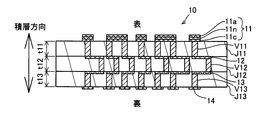
- FIG. 2 is an explanatory view of a cross section of the first wiring board 10.
- FIG. 2 shows a schematic view of the cross section of the wiring board 10 enlarged only in the stacking direction.
- the first wiring board 10 of the present embodiment is a board in which a plurality of resin layers J11 to J13 formed of polyimide, which is a thermosetting resin, are laminated. Between the resin layers J11 to J13, wiring layers 12 and 13 having a predetermined pattern formed in contact with the resin layers J11 to J13 are formed. Further, a connection terminal 11 is formed on the front surface of the resin layer J11, and a connection terminal 14 is formed on the back surface of the resin layer J13.
- connection terminals 11 and 14 are formed on the front surface and the back surface of the first wiring board 10.
- the connection terminal 11 is a terminal in which a Cu (copper) layer 11c, a Ni (nickel) layer 11n, and an Au (gold) layer 11a are laminated in order from the surface of the resin layer J11.
- the wiring layers 12 and 13 and the connection terminal 14 are formed of Cu—Ti.
- the resin layer J11 is formed with a via conductor V11 that electrically connects the connection terminal 11 and the wiring layer 12.
- the resin layer J12 is formed with a via conductor V12 that electrically connects the wiring layer 12 and the wiring layer 13.
- the resin layer J13 is formed with a via conductor V13 that electrically connects the wiring layer 13 and the connection terminal 14.
- Each via conductor V11 to V13 is formed of Cu—Ti.
- the via conductors V11 to V13 electrically connect the connection terminal 11 formed on the front surface of the first wiring board 10 and the connection terminal 14 formed on the back surface.
- the first wiring board 10 of the present embodiment is not manufactured by laminating the resin layers J11 to J13 separately and then collectively laminating them, but the wiring layer 13 and the resin layer J12 are manufactured with respect to the resin layer J13.
- the wiring layer 12, the resin layer J11, and the wiring layer 11 are formed in this order by a build-up method. Therefore, the thicknesses t11 to t13 along the stacking direction of the resin layers J11 to J13 of the present embodiment are thinner than the thickness when the resin layers J11 to J13 are prepared separately.
- FIG. 3 is a schematic cross-sectional view of the joining layer 30 before joining the first wiring board 10 and the second wiring board 20.
- FIG. 3 shows an enlarged cross-sectional view of a part of the bonding layer 30.
- the bonding layer 30 includes a base material 31 formed of polyimide which is a thermosetting resin, bonding materials 32 and 33 arranged on both sides of the base material 31, and a conductive member 34. I have.
- the bonding materials 32 and 33 are formed of a thermoplastic resin polyimide, which is different from the base material 31.
- the polyimide of the thermoplastic resin and the polyimide of the thermosetting resin are distinguished by the glass transition point.
- a resin having a glass transition point of 300 ° C. or higher is defined as a thermosetting resin
- a resin having a glass transition point of less than 300 ° C. is defined as a thermoplastic resin.
- the glass transition point can be specified by, for example, the TMA method (Thermo Mechanical Analysis).
- the glass transition point of the polyimide of the thermoplastic resin in the present embodiment is 240 ° C.
- the glass transition point of the polyimide of the thermosetting resin is 420 ° C.
- the thickness t31 along the laminating direction of the base material 31 is 10 to 100 ⁇ m. In this example, it is 30 ⁇ m. Further, the thicknesses t32 and t33 of the bonding materials 32 and 33 along the laminating direction can be 15 ⁇ m or less. In this embodiment, the thicknesses t32 and t33 are the same and are 3 ⁇ m. In the present embodiment, the thickness (t31 + t32 + t33) of the bonding layer 30, which is the total of the base material 31 and the bonding materials 32 and 33, is thicker than one layer (for example, J11) of the first wiring board 10. In other words, the thickness (for example, t11) of each layer of the first wiring board 10 along the stacking direction is formed to be thinner than the thickness of the bonding layer 30.
- the conductive member 34 is formed of Ag.
- the conductive member 34 is formed so as to penetrate the bonding layer 30 (base material 31 and bonding materials 32, 33). As shown in FIG. 3, the conductive member 34 protrudes from the joining members 32 and 33 to the front surface and the back surface along the thickness direction.
- the conductive member 34 formed in the joint layer 30 has a connection terminal 14 formed on the back surface of the first wiring board 10 and a connection formed on the front surface of the second wiring board 20. It is formed at each position to connect to the terminal 23. That is, the conductive member 34 electrically connects the connection terminal 14 on the back surface of the first wiring board 10 and the connection terminal 23 on the front surface of the second wiring board 20.
- FIG. 4 is a flowchart of a manufacturing method of the multilayer wiring board 100.
- the method for manufacturing the multilayer wiring board 100 first, the first wiring board 10, the second wiring board 20, and the bonding layer 30 of each sample constituting the multilayer wiring board 100 are prepared (step S1). After that, the conductive member 34 of the bonding layer 30 is laminated in a batch in a state of being arranged at a position where the connection terminal 14 of the first wiring board 10 and the connection terminal 23 of the second wiring board 20 are connected. Step S2), the multilayer wiring board 100 is manufactured. Heat is applied to the bonding layer 30 when the layers are laminated together.
- the bonding materials 32 and 33 which are the thermoplastic resins of the bonding layer 30, are changed, the first wiring board 10 and the bonding layer 30 are bonded, and the bonding layer 30 and the second wiring board 20 are bonded to each other. Join. As a result, the first wiring board 10 and the second wiring board 20 are joined via the joining layer 30.
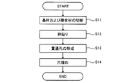
- FIG. 5 and 6 are explanatory views of a method for manufacturing the bonding layer 30.
- FIG. 5 shows a flowchart of a method for manufacturing the bonding layer 30.
- FIG. 6 shows a part of the cross section of the bonding layer 30 that changes according to the flowchart in accordance with each step shown in FIG.
- the sheet of the bonding layer 30 in which the bonding materials 32 and 33 are formed on both surfaces of the base material 31 is cut into a predetermined size (step S11).
- a frame is attached to the joint layer 30 after cutting (step S12).
- a through hole HL penetrating in the thickness direction is formed in the joint layer 30 by a laser punch (step S13).
- the formed through hole HL is filled with Ag, which is the source of the conductive member 34 (step S14), and the method for manufacturing the bonding layer 30 is completed.
- the first wiring board 10 having the wiring layers 12 and 13 and the front surface of the second wiring board 20 made of ceramic are first.
- a bonding layer 30 for joining the wiring board 10 and the second wiring board 20 is provided.
- the surface of the bonding layer 30 adjacent to the second wiring board 20 is formed of a thermoplastic resin bonding material 33. That is, the first wiring board 10 and the second wiring board 20 are joined by the thermoplastic resin forming the joining material 33. Therefore, when heat is applied to the multilayer wiring board 100, the thermoplastic resin changes, and the bonding between the first wiring board 10 and the second wiring board 20 is released.
- the first wiring board 10 is formed of a plurality of layers formed of a thermosetting resin, the bonding between the layers is not released even when heat is applied.
- the completed multilayer wiring board 100 can be removed from the first wiring board 10 and the second wiring board 20, and the first wiring board 10 and the second wiring board 20 can be reused. ..
- the manufacturing man-hours of the multilayer wiring board 100 can be reduced by reusing the second wiring board 20 which requires a large number of manufacturing man-hours.
- prefabricating a common ceramic that can be used for many multilayer wiring boards 100 the man-hours for manufacturing the multilayer wiring board 100 are reduced.
- the bonding layer 30 of the present embodiment is a bonding material 32, 33 of a base material 31 formed of a thermosetting resin and a thermoplastic resin arranged on both sides of the base material 31. And have. Further, the bonding layer 30 is formed with a conductive member 34 penetrating in the stacking direction. The conductive member 34 electrically connects the connection terminal 14 on the back surface of the first wiring board 10 and the connection terminal 23 on the front surface of the second wiring board 20. Since the base material 31 is formed of a thermosetting resin, it is less likely to be deformed than the bonding materials 32 and 33 formed of a thermoplastic resin. Therefore, the first wiring board 10 and the second wiring board 20 are joined in a state where the joining can be released by the joining materials 32 and 33, and then electrically stably connected by the base material 31 which is hard to be deformed. Will be done.
- the thickness of one layer (for example, the resin layer J11) in the first wiring board 10 of the present embodiment along the stacking direction is thinner than the thickness of the bonding layer 30. Therefore, the thickness of the entire first wiring board 10 can be reduced. As a result, the number of layers of the wiring layer constituting the first wiring board 10 can be increased, and the circuit formed by the wiring layer can be thinned.
- the first wiring board 10 of the above embodiment is a laminated body of three resin layers J11 to J13, but the number of laminated layers may be two or four. It may be one or more.
- the thickness along the stacking direction of each layer (for example, t11) does not have to be thinner than the thickness of the bonding layer 30.
- Each layer may be a mixture of a layer thinner than the bonding layer 30 and a layer thicker than the bonding layer 30.
- the resin layers J11 to J13 of the above-described embodiment are formed of polyimide, which is a thermosetting resin, but may be formed of other thermosetting resin.
- connection terminal 11 and 14 and the wiring layers 12 and 13 can be deformed.
- the connection terminal 11 formed on the surface of the first wiring board 10 was a terminal in which three metals of Au, Ni, and Cu were laminated, but it may be formed of one kind of metal, or another. It may be made of the same metal (for example, Ag).
- the connection terminal 14 can be omitted.
- the via conductor V13 in the resin layer J13 and the conductive member 34 penetrating the joint layer 30 may be directly connected.
- the via conductors V11 to V13 penetrating the resin layers J11 to J13 may be formed of a conductive material other than Cu and Ti (titanium), and may be formed of, for example, Ag.
- the second wiring board 20 of the above embodiment is a laminated body of three ceramic layers C21 to C23 made of ceramic, but it may be a laminated body of four or more layers. Alternatively, for example, it may be formed of a single layer of only the ceramic layer C21.
- the material forming the ceramic layers C21 to C23 may be, for example, AlN (aluminum nitride), glass-ceramic, mullite, or BN as a ceramic other than aluminum oxide. Further, each layer may be formed of different ceramics. The thickness of each of the ceramic layers C21 to C23 along the stacking direction may not be the same or may be different.
- the predetermined patterns of the wiring layers 21 and 23 and the connection terminals 23 and 24 are deformable.
- the via conductors V21 to 23 penetrating the ceramic layers C21 to C23 may be formed of a conductive material other than W, for example, Mo (molybdenum), a material in which Mo and W are mixed, or Cu.
- the bonding layer 30 of the above embodiment is a layer in which the bonding materials 32 and 33 of the thermoplastic resin are formed on both sides using the base material 31 as a base material, but the structure of the bonding layer 30 can be variously modified. ..
- the bonding layer 30 only the bonding material 33 on the back surface adjacent to the second wiring board 20 may be formed of the thermoplastic resin, and the bonding material 32 on the front surface may not be present.
- the entire bonding layer 30 is formed of a thermoplastic resin, and the bonding layer 30 does not have to contain a thermosetting resin.
- the thicknesses t31 to t33 of the base material 31 and the bonding materials 32 and 33 in the above embodiment are examples, and may have other dimensions.
- the conductive member 34 may be formed of a material other than Ag, and may be formed of, for example, Cu, W, Mo, Ta (tantalum) or the like.
- thermoplastic resin used for the bonding layer 30 examples include acrylonitrile-butadiene-styrene copolymer synthetic resin (ABS), nylon, polypropylene (PP), polycarbonate (PC), polyamide (PA) nylon, polyacetyl (POM), and the like.
- ABS acrylonitrile-butadiene-styrene copolymer synthetic resin
- PP polypropylene
- PC polycarbonate
- PA polyamide
- POM polyacetyl
- PBT polybutylene terephthalate
- PEI polyetherimide
- PPS polyphenylene sulfide
- PEEK polyetheretherketone
- LCP liquid crystal polymer
- PPA polyphthalamide
- PSU polysulfone
- PES polyethersulfone
- PAI polyamideimide
- thermosetting resin used for the base material 31 of the bonding layer 30 examples include epoxy resin, phenol resin, urea, melamine, unsaturated polyester, polyurethane, diallyl phthalate, silicone, and alkyd.
Landscapes
- Engineering & Computer Science (AREA)
- Microelectronics & Electronic Packaging (AREA)
- Manufacturing & Machinery (AREA)
- Chemical & Material Sciences (AREA)
- Ceramic Engineering (AREA)
- Inorganic Chemistry (AREA)
- Physics & Mathematics (AREA)
- General Physics & Mathematics (AREA)
- Production Of Multi-Layered Print Wiring Board (AREA)
Abstract
多層配線基板は、熱硬化性樹脂で形成された複数の層を積層してなり、各層の間に層と接触した状態で形成された配線層を有する第1の配線基板と、セラミックからなる第2の配線基板と、第1の配線基板の裏面と第2の配線基板の表面との間に配置され、第1の配線基板と第2の配線基板とを接合する接合層と、を備え、接合層のうち、少なくとも第2の配線基板に隣接する面は、熱可塑性樹脂によって形成されている。
Description
本発明は、多層配線基板に関する。
複数の樹脂層が積層された樹脂基板と、接続端子を有するセラミック基板とが一括で積層された多層配線基板が知られている(例えば、特許文献1参照)。特許文献1に記載された多層配線基板では、複数の樹脂層のそれぞれが個別に作製された後に、樹脂基板とセラミック基板とが一括で積層されている。特許文献2に記載された配線基板は、セラミック基板の表面と配線層の裏面とを接合する接合層を備えている。この接合層は、熱硬化性樹脂からなるコア層と、コア層よりも弾性率が小さい熱硬化性樹脂からなる接着層とを有している。
多層配線基板に用いられるセラミックの製造工数は、他の部品の製造工数と比べて多い。このため、多層配線基板全体の製造工数が多くなり、多層配線基板の製造にかかる時間が長くなる場合がある。特許文献1および特許文献2には、多層配線基板における各層の製造方法に開示されているものの、多層配線基板およびセラミックの製造工数について何ら考慮されていない。多層配線基板の製造工数を少なくするために、製造工数が多いセラミックを再利用したいという要望があった。
本発明は、上述した課題を解決するためになされたものであり、再利用が可能な多層配線基板に用いられるセラミックの基板を提供することを目的とする。
本発明は、上述の課題を解決するためになされたものであり、以下の形態として実現できる。
(1)本発明の一形態によれば、多層配線基板が提供される。この多層配線基板は、熱硬化性樹脂で形成された複数の層を積層してなり、各前記層の間に前記層と接触した状態で形成された配線層を有する第1の配線基板と、セラミックからなる第2の配線基板と、前記第1の配線基板の裏面と前記第2の配線基板の表面との間に配置され、前記第1の配線基板と前記第2の配線基板とを接合する接合層と、を備え、前記接合層のうち、少なくとも前記第2の配線基板に隣接する面は、熱可塑性樹脂によって形成されている。
この構成によれば、第1の配線基板の裏面と、第2の配線基板の表面とを接合する接合層のうち、第2の配線基板の表面に隣接する面は、熱可塑性樹脂によって形成されている。そのため、第1の配線基板と第2の配線基板とが接合された後であっても、多層配線基板に熱が加えられることによって熱可塑性樹脂が変化し、第1の配線基板と第2の配線基板との接合が解除される。一方で、熱硬化性樹脂によって接合されている第1の配線基板における各層間の接合は解除されない。この結果、第1の配線基板と第2の配線基板とを容易に取り外すことができ、第1の配線基板及び第2の配線基板の再利用が可能になる。これにより、製造工数の多い第2の配線基板を再利用することにより、多層配線基板の製造工数を少なくできる。また、多くの多層配線基板に適用可能なセラミックが予め作製されることによって、多層配線基板の製造工数が少なくなる。
(2)上記態様の多層配線基板において、前記第1の配線基板及び前記第2の配線基板は、それぞれ表面及び裏面に接続端子が形成され、前記第1の配線基板の裏面の接続端子と、前記第2の配線基板の表面の接続端子とは、前記接合層を貫通するように形成された導電部材を介して電気的に接続され、前記接合層は、熱硬化性樹脂によって形成された基材と、前記基材の両面に配置されて、前記第1の配線基板と前記第2の配線基板とを接合する接合材であって、熱可塑性樹脂によって形成された接合材と、を有していてもよい。
この構成によれば、接合層は、両面に熱可塑性樹脂によって形成された接合材と、両面の接合材に挟まれる基材とを有している。基材は、熱硬化性樹脂によって形成されているため、第1配線層と第2配線層とを接合するときの熱が接合層に加わっても、変形しにくい。そのため、第1の配線基板と第2の配線基板とは、接合材によって接合を解除できる状態で接合された上で、変形しにくい基材31によって電気的に安定して接続される。
この構成によれば、接合層は、両面に熱可塑性樹脂によって形成された接合材と、両面の接合材に挟まれる基材とを有している。基材は、熱硬化性樹脂によって形成されているため、第1配線層と第2配線層とを接合するときの熱が接合層に加わっても、変形しにくい。そのため、第1の配線基板と第2の配線基板とは、接合材によって接合を解除できる状態で接合された上で、変形しにくい基材31によって電気的に安定して接続される。
(3)上記態様の多層配線基板において、前記第1の配線基板と前記接合層と前記第2の配線基板との積層方向において、前記第1の配線基板のうちの1つの前記層の厚さは、前記接合層の厚さよりも薄くてもよい。
この構成によれば、第1の配線基板に含まれる各層の積層方向に沿う厚さが、接合層の厚さよりも小さい。すなわち、本構成では、第1の配線基板の厚さを薄くできる。これにより、第1の配線基板を構成する配線層の層数を増やすことができ、配線層が構成する回路の細線化を実行できる。
この構成によれば、第1の配線基板に含まれる各層の積層方向に沿う厚さが、接合層の厚さよりも小さい。すなわち、本構成では、第1の配線基板の厚さを薄くできる。これにより、第1の配線基板を構成する配線層の層数を増やすことができ、配線層が構成する回路の細線化を実行できる。
なお、本発明は、種々の態様で実現することが可能であり、例えば、配線基板、多層配線基板、半導体用配線基板、およびこれらを備える部品、配線基板または多層配線基板の製造方法等の形態で実現することができる。
<実施形態>
図1は、本発明の実施形態としての多層配線基板100の概略断面図である。本実施形態の多層配線基板100は、半導体検査に使用されるプローブカードとして用いられる。プローブカードは、シリコンウェハーに形成された複数の電子部品の電気時特性を検査するための器具である。図1には、多層配線基板100を形成する各層の積層方向に沿う断面の概略が示されている。
図1は、本発明の実施形態としての多層配線基板100の概略断面図である。本実施形態の多層配線基板100は、半導体検査に使用されるプローブカードとして用いられる。プローブカードは、シリコンウェハーに形成された複数の電子部品の電気時特性を検査するための器具である。図1には、多層配線基板100を形成する各層の積層方向に沿う断面の概略が示されている。
図1に示されるように、多層配線基板100は、熱硬化性樹脂で形成された複数の樹脂層が積層された第1の配線基板10と、セラミックで形成された第2の配線基板20と、第1の配線基板10の裏面と第2の配線基板20の表面との間に配置された接合層30と、を備えている。なお、図1では、第1の配線基板10の詳細についての図示を省略し、第1の配線基板10の詳細については図2と合わせて説明する。
図1に示されるように、第2の配線基板20は、セラミックで形成された3つのセラミック層C21~C23が積層された基板である。本実施形態では、3つのセラミック層C21~C23のそれぞれは、酸化アルミニウムで形成され、同じ厚さを有する基板である。セラミック層C21の表面には、接続端子23が形成されている。セラミック層C22,C23のそれぞれの表面には、所定パターンの配線層21,22が形成されている。また、セラミック層C23の裏面には、接続端子24が形成されている。すなわち、第2の配線基板20の表面及び裏面に接続端子23,24が形成されている。
セラミック層C21には、表面に形成された接続端子23と配線層21とを電気的に接続するビア導体V21が形成されている。同じように、セラミック層C22には、配線層21と配線層22とを電気的に接続するビア導体V22が形成されている。セラミック層C23には、配線層22と、裏面に形成された接続端子24とを接続するビア導体V23が形成されている。各ビア導体V21~V23は、W(タングステン)によって形成されている。ビア導体V21~V23によって、第2の配線基板20の表面に形成された接続端子23と、裏面に形成された接続端子24とが電気的に接続される。
図2は、第1の配線基板10の断面の説明図である。図2には、配線基板10の断面を、積層方向のみに拡大した概略図が示されている。図2に示されるように、本実施形態の第1の配線基板10は、熱硬化性樹脂であるポリイミドで形成された複数の樹脂層J11~J13が積層された基板である。各樹脂層J11~J13の間には、各樹脂層J11~J13と接触した状態で形成された所定パターンの配線層12,13が形成されている。また、樹脂層J11の表面には、接続端子11が形成され、樹脂層J13の裏面には、接続端子14が形成されている。すなわち、第1の配線基板10の表面及び裏面には接続端子11,14が形成されている。接続端子11は、樹脂層J11の表面から順番に、Cu(銅)層11c,Ni(ニッケル)層11n,Au(金)層11aが積層された端子である。配線層12,13及び接続端子14は、Cu-Tiによって形成されている。
樹脂層J11には、接続端子11と配線層12とを電気的に接続するビア導体V11が形成されている。同じように、樹脂層J12には、配線層12と配線層13とを電気的に接続するビア導体V12が形成されている。樹脂層J13には、配線層13と接続端子14とを電気的に接続するビア導体V13が形成されている。各ビア導体V11~V13は、Cu-Tiによって形成されている。ビア導体V11~V13によって、第1の配線基板10の表面に形成された接続端子11と、裏面に形成された接続端子14とが電気的に接続される。
本実施形態の第1の配線基板10は、各樹脂層J11~J13が別々に用意された後に一括積層されて製造されるのではなく、樹脂層J13に対して、配線層13,樹脂層J12,配線層12,樹脂層J11,配線層11の順に形成されるビルドアップ工法によって製造されている。そのため、本実施形態の各樹脂層J11~J13の積層方向に沿う厚さt11~t13は、各樹脂層J11~J13が別々に用意された場合の厚さよりも薄い。
図3は、第1の配線基板10と第2の配線基板20とを接合する前の接合層30の概略断面図である。図3には、接合層30の一部を拡大した断面図が示されている。図3に示されるように、接合層30は、熱硬化性樹脂であるポリイミドによって形成された基材31と、基材31の両面に配置された接合材32,33と、導電部材34とを備えている。接合材32,33は、基材31と異なる、熱可塑性樹脂のポリイミドによって形成されている。
本実施形態では、熱可塑性樹脂のポリイミドと、熱硬化性樹脂のポリイミドとは、ガラス転移点によって区別している。具体的には、ガラス転移点が300℃以上の樹脂を熱硬化性樹脂として定義し、ガラス転移点が300℃未満の樹脂を熱可塑性樹脂として定義している。ガラス転移点は、例えば、TMA法(Thermo Mechanical Analysis)などによって特定できる。本実施形態における熱可塑性樹脂のポリイミドのガラス転移点は、240℃であり、熱硬化性樹脂のポリイミドのガラス転移点は、420℃である。
基材31の積層方向に沿う厚さt31は、10~100μmのものを用いる。本実施例では、30μmである。また、接合材32,33の積層方向に沿うそれぞれの厚さt32,t33は、15μm以下のものを用いることができる。本実施例では、厚さt32,t33は、同じであり、3μmである。本実施形態では、基材31および接合材32,33の合計である接合層30の厚さ(t31+t32+t33)は、第1の配線基板10の1つの層(例えばJ11)よりも厚い。換言すると、第1の配線基板10の各層の積層方向に沿う厚さ(例えばt11)は、接合層30の厚さよりも薄く形成されている。
導電部材34は、Agによって形成されている。導電部材34は、接合層30(基材31および接合材32,33)を貫通するように形成されている。図3に示されるように、導電部材34は、厚さ方向に沿って接合材32,33よりも表面及び裏面に飛び出している。図1に示されるように、接合層30に形成される導電部材34は、第1の配線基板10の裏面に形成された接続端子14と、第2の配線基板20の表面に形成された接続端子23とを接続するそれぞれの位置に形成されている。すなわち、導電部材34は、第1の配線基板10の裏面の接続端子14と、第2の配線基板20の表面の接続端子23とを電気的に接続する。
図4は、多層配線基板100の製造方法のフローチャートである。多層配線基板100の製造方法では、初めに、多層配線基板100を構成する各サンプルの第1の配線基板10、第2の配線基板20、および接合層30を準備する(ステップS1)。その後、接合層30の導電部材34が、第1の配線基板10の接続端子14と、第2の配線基板20の接続端子23とを接続する位置に配置された状態で、一括で積層され(ステップS2)、多層配線基板100が製造される。一括で積層される際に、接合層30に熱が加えられる。これにより、接合層30の熱可塑性樹脂である接合材32,33が変化し、第1の配線基板10と接合層30とを接合し、かつ、接合層30と第2の配線基板20とを接合する。その結果、第1の配線基板10と第2の配線基板20とは、接合層30を介して接合される。
図5および図6は、接合層30の製造方法の説明図である。図5には、接合層30の製造方法のフローチャートが示されている。図6には、フローチャートに沿って変化する接合層30の断面の一部が、図5に示される各ステップに合わせて示されている。接合層30の製造方法では、初めに、基材31の両面に接合材32,33が形成された接合層30のシートが所定の大きさに切断される(ステップS11)。切断後の接合層30に対して枠貼りが行われる(ステップS12)。
接合層30に対して、レーザパンチによって、厚さ方向に貫通する貫通孔HLが形成される(ステップS13)。形成された貫通孔HLは、導電部材34の元となるAgによって穴埋めされ(ステップS14)、接合層30の製造方法が終了する。
以上説明したように、本実施形態の多層配線基板100は、配線層12,13を有する第1の配線基板10裏面と、セラミックからなる第2の配線基板20の表面との間に、第1の配線基板10と第2の配線基板20とを接合する接合層30を備えている。接合層30の内、第2の配線基板20に隣接する面は、熱可塑性樹脂の接合材33で形成されている。すなわち、第1の配線基板10と第2の配線基板20とは、接合材33を形成している熱可塑性樹脂によって接合されている。そのため、多層配線基板100に熱が加えられると、熱可塑性樹脂が変化し、第1の配線基板10と第2の配線基板20との接合が解除される。一方で、第1の配線基板10は、熱硬化性樹脂で形成された複数の層から形成されているため、熱を加えられても各層間の接合は解除されない。この結果、完成した多層配線基板100を第1の配線基板10と第2の配線基板20とに取り外すことができ、第1の配線基板10及び第2の配線基板20の再利用が可能になる。これにより、製造工数の多い第2の配線基板20を再利用することで、多層配線基板100の製造工数を少なくできる。また、多くの多層配線基板100に利用可能な共通のセラミックが予め作製されることによって、多層配線基板100の製造工数が少なくなる。
また、本実施形態の接合層30は、図3に示されるように、熱硬化性樹脂によって形成された基材31と、基材31の両面に配置された熱可塑性樹脂の接合材32,33とを備えている。さらに、接合層30には、積層方向に貫通する導電部材34が形成されている。導電部材34は、第1の配線基板10の裏面の接続端子14と、第2の配線基板20の表面の接続端子23とを電気的に接続している。基材31は、熱硬化性樹脂によって形成されているため、熱可塑性樹脂で形成された接合材32,33よりも変形しにくい。そのため、第1の配線基板10と第2の配線基板20とは、接合材32,33によって接合を解除できる状態で接合された上で、変形しにくい基材31によって電気的に安定して接続される。
また、本実施形態の第1の配線基板10における1つの層(例えば樹脂層J11)の積層方向に沿う厚さは、接合層30の厚さよりも薄い。そのため、第1の配線基板10全体の厚さを薄くできる。これにより、第1の配線基板10を構成する配線層の層数を増やすことができ、配線層が構成する回路の細線化を実行できる。
<本実施形態の変形例>
本発明は上記の実施形態に限られるものではなく、その要旨を逸脱しない範囲において種々の態様において実施することが可能であり、例えば次のような変形も可能である。
本発明は上記の実施形態に限られるものではなく、その要旨を逸脱しない範囲において種々の態様において実施することが可能であり、例えば次のような変形も可能である。
[変形例1]
上記実施形態では、多層配線基板100を構成する第1の配線基板10、第2の配線基板20、および接合層30の一例について説明したが、多層配線基板100の各構成および各形状については、種々変形可能である。上記実施形態の第1の配線基板10は、図2に示されるように、3つの樹脂層J11~J13の積層体であったが、各層の積層数は2つであってもよいし、4つ以上であってもよい。各層の積層方向に沿う厚さ(例えば、t11)は、接合層30の厚さよりも薄くなくてもよい。各層は、接合層30よりも薄い層と厚い層とが混合されていてもよい。上記実施形態の樹脂層J11~J13は、熱硬化性樹脂のポリイミドで形成されていたが、その他の熱硬化性樹脂で形成されていてもよい。
上記実施形態では、多層配線基板100を構成する第1の配線基板10、第2の配線基板20、および接合層30の一例について説明したが、多層配線基板100の各構成および各形状については、種々変形可能である。上記実施形態の第1の配線基板10は、図2に示されるように、3つの樹脂層J11~J13の積層体であったが、各層の積層数は2つであってもよいし、4つ以上であってもよい。各層の積層方向に沿う厚さ(例えば、t11)は、接合層30の厚さよりも薄くなくてもよい。各層は、接合層30よりも薄い層と厚い層とが混合されていてもよい。上記実施形態の樹脂層J11~J13は、熱硬化性樹脂のポリイミドで形成されていたが、その他の熱硬化性樹脂で形成されていてもよい。
接続端子11,14および配線層12,13の所定パターンについては、変形可能である。第1の配線基板10の表面に形成された接続端子11は、Au,Ni,Cuの3つの金属が積層された端子であったが、1種類の金属で形成されていてもよく、または他の金属(例えば、Agなど)で形成されていてもよい。接続端子14は、省略可能であり、例えば、樹脂層J13内のビア導体V13と、接合層30を貫通する導電部材34とが直接接続されていてもよい。各樹脂層J11~J13を貫通する各ビア導体V11~13は、Cu,Ti(チタン)以外の導電性材料で形成されていてもよく、例えば、Agなどで形成されていてもよい。
上記実施形態の第2の配線基板20は、図1に示されるように、セラミックからなる3つのセラミック層C21~C23の積層体であったが、4つ以上の層の積層体であってもよいし、例えば、セラミック層C21のみの単層で形成されていてもよい。セラミック層C21~C23を形成する材質は、酸化アルミニウム以外のセラミックとして、例えば、AlN(窒化アルミニウム)、ガラス-セラミック、ムライト、BNであってもよい。また、各層が異なるセラミックによって形成されていてもよい。各セラミック層C21~C23の積層方向に沿う厚さは、同じでなくてもよく、異なっていてもよい。配線層21,23及び接続端子23,24の所定パターンは、変形可能である。各セラミック層C21~C23を貫通する各ビア導体V21~23は、W以外の導電性材料、例えば、Mo(モリブデン),MoとWとを混ぜた材料、Cuで形成されていてもよい。
上記実施形態の接合層30は、基材31を母材として両面に、熱可塑性樹脂の接合材32,33が形成された層であったが、接合層30の構成については種々変形可能である。例えば、接合層30のうち、少なくとも第2の配線基板20に隣接する裏面の接合材33のみが熱可塑性樹脂によって形成され、表面の接合材32が存在しなくてもよい。また、接合層30全体が熱可塑性樹脂によって形成されており、接合層30が熱硬化性樹脂を含まなくてもよい。上記実施形態における基材31及び接合材32,33の各厚さt31~t33については、一例であり、その他の寸法であってもよい。導電部材34は、Ag以外の材料で形成されていてもよく、例えば、Cu,W,Mo,Ta(タンタル)などで形成されていてもよい。
接合層30に用いられる熱可塑性樹脂としては、例えば、アクリロニトリル・ブタジエン・スチレン共重合合成樹脂(ABS)、ナイロン、ポリプロピレン(PP)、ポリカーボネート(PC)、ポリアミド(PA)ナイロン、ポリアセタール(POM)、ポリブチレンテレフタレート(PBT)、ポリエーテルイミド(PEI)、ポリフェニレンサルファイド(PPS)、ポリエーテルエーテルケトン(PEEK)、液晶性ポリマー(LCP)、ポリフタールアミド(PPA)、ポリスルホン(PSU)、ポリエーテルスルホン(PES)、およびポリアミドイミド(PAI)などが挙げられる。
接合層30の基材31に用いられる熱硬化性樹脂としては、例えば、エポキシ樹脂、フェノール樹脂、尿素、メラミン、不飽和ポリエステル、ポリウレタン、ジアリルフタレート、シリコーン、およびアルキッドなどが挙げられる。
以上、実施形態、変形例に基づき本態様について説明してきたが、上記した態様の実施の形態は、本態様の理解を容易にするためのものであり、本態様を限定するものではない。本態様は、その趣旨並びに特許請求の範囲を逸脱することなく、変更、改良され得ると共に、本態様にはその等価物が含まれる。また、その技術的特徴が本明細書中に必須なものとして説明されていなければ、適宜、削除することができる。
10…第1の配線基板
11,14…接続端子
11a…Au層
11c…Cu層
11n…Ni層
12,13…配線層
20…第2の配線基板
21,22…配線層
23,24…接続端子
30…接合層
31…基材
32,33…接合材
34…導電部材
100…多層配線基板
C21~C23…セラミック層
HL…貫通孔
J11,J12,J13…樹脂層
V11~V13…ビア導体
V21~V23…ビア導体
t11~t13,t31~t33…厚さ
11,14…接続端子
11a…Au層
11c…Cu層
11n…Ni層
12,13…配線層
20…第2の配線基板
21,22…配線層
23,24…接続端子
30…接合層
31…基材
32,33…接合材
34…導電部材
100…多層配線基板
C21~C23…セラミック層
HL…貫通孔
J11,J12,J13…樹脂層
V11~V13…ビア導体
V21~V23…ビア導体
t11~t13,t31~t33…厚さ
Claims (3)
- 多層配線基板であって、
熱硬化性樹脂で形成された複数の層を積層してなり、各前記層の間に前記層と接触した状態で形成された配線層を有する第1の配線基板と、
セラミックからなる第2の配線基板と、
前記第1の配線基板の裏面と前記第2の配線基板の表面との間に配置され、前記第1の配線基板と前記第2の配線基板とを接合する接合層と、
を備え、
前記接合層のうち、少なくとも前記第2の配線基板に隣接する面は、熱可塑性樹脂によって形成されていることを特徴とする、多層配線基板。 - 請求項1に記載の多層配線基板であって、
前記第1の配線基板及び前記第2の配線基板は、それぞれ表面及び裏面に接続端子が形成され、
前記第1の配線基板の裏面の接続端子と、前記第2の配線基板の表面の接続端子とは、前記接合層を貫通するように形成された導電部材を介して電気的に接続され、
前記接合層は、
熱硬化性樹脂によって形成された基材と、
前記基材の両面に配置されて、前記第1の配線基板と前記第2の配線基板とを接合する接合材であって、熱可塑性樹脂によって形成された接合材と、
を有することを特徴とする、多層配線基板。 - 請求項1または請求項2に記載の多層配線基板であって、
前記第1の配線基板と前記接合層と前記第2の配線基板との積層方向において、前記第1の配線基板のうちの1つの前記層の厚さは、前記接合層の厚さよりも薄いことを特徴とする、多層配線基板。
Priority Applications (4)
| Application Number | Priority Date | Filing Date | Title |
|---|---|---|---|
| KR1020217025195A KR102537662B1 (ko) | 2019-11-08 | 2020-05-22 | 다층 배선 기판 |
| CN202080013476.2A CN113412686B (zh) | 2019-11-08 | 2020-05-22 | 多层布线基板 |
| EP20884642.8A EP4057784A4 (en) | 2019-11-08 | 2020-05-22 | MULTILAYER WIRING BOARD |
| US17/429,666 US20220108943A1 (en) | 2019-11-08 | 2020-05-22 | Multilayer wiring substrate |
Applications Claiming Priority (2)
| Application Number | Priority Date | Filing Date | Title |
|---|---|---|---|
| JP2019202914A JP7223672B2 (ja) | 2019-11-08 | 2019-11-08 | 多層配線基板 |
| JP2019-202914 | 2019-11-08 |
Publications (1)
| Publication Number | Publication Date |
|---|---|
| WO2021090527A1 true WO2021090527A1 (ja) | 2021-05-14 |
Family
ID=75849840
Family Applications (1)
| Application Number | Title | Priority Date | Filing Date |
|---|---|---|---|
| PCT/JP2020/020311 Ceased WO2021090527A1 (ja) | 2019-11-08 | 2020-05-22 | 多層配線基板 |
Country Status (7)
| Country | Link |
|---|---|
| US (1) | US20220108943A1 (ja) |
| EP (1) | EP4057784A4 (ja) |
| JP (1) | JP7223672B2 (ja) |
| KR (1) | KR102537662B1 (ja) |
| CN (1) | CN113412686B (ja) |
| TW (1) | TWI761839B (ja) |
| WO (1) | WO2021090527A1 (ja) |
Families Citing this family (1)
| Publication number | Priority date | Publication date | Assignee | Title |
|---|---|---|---|---|
| KR20220160967A (ko) * | 2021-05-28 | 2022-12-06 | (주)티에스이 | 이종 재질의 다층 회로기판 및 그 제조 방법 |
Citations (4)
| Publication number | Priority date | Publication date | Assignee | Title |
|---|---|---|---|---|
| JP2008218443A (ja) * | 2007-02-28 | 2008-09-18 | Micronics Japan Co Ltd | 多層配線基板及びその検査方法 |
| WO2013031822A1 (ja) | 2011-08-29 | 2013-03-07 | 京セラ株式会社 | 薄膜配線基板およびプローブカード用基板 |
| JP2015002262A (ja) * | 2013-06-14 | 2015-01-05 | 日本特殊陶業株式会社 | 多層配線基板の製造方法 |
| JP2017037929A (ja) | 2015-08-07 | 2017-02-16 | 日本特殊陶業株式会社 | 多層配線基板およびその製造方法 |
Family Cites Families (20)
| Publication number | Priority date | Publication date | Assignee | Title |
|---|---|---|---|---|
| JPS6180896A (ja) * | 1984-09-28 | 1986-04-24 | 株式会社日立製作所 | 多層配線基板 |
| JP4186236B2 (ja) * | 1996-06-20 | 2008-11-26 | 富士通マイクロエレクトロニクス株式会社 | ポリイミド多層配線フィルムの製造方法及び多層配線基板の製造方法 |
| US6600224B1 (en) * | 2000-10-31 | 2003-07-29 | International Business Machines Corporation | Thin film attachment to laminate using a dendritic interconnection |
| JP3840921B2 (ja) | 2001-06-13 | 2006-11-01 | 株式会社デンソー | プリント基板のおよびその製造方法 |
| US6768064B2 (en) * | 2001-07-10 | 2004-07-27 | Fujikura Ltd. | Multilayer wiring board assembly, multilayer wiring board assembly component and method of manufacture thereof |
| JP2003318545A (ja) * | 2002-04-22 | 2003-11-07 | Sony Corp | 多層型プリント配線基板及び多層型プリント配線基板の製造方法 |
| US20050175850A1 (en) * | 2002-11-20 | 2005-08-11 | Tomoegawa Paper Co., Ltd | Flexible metal laminate and heat-resistant adhesive composition |
| JP2005144816A (ja) * | 2003-11-13 | 2005-06-09 | Tomoegawa Paper Co Ltd | フレキシブル金属積層体 |
| JP4786914B2 (ja) | 2005-02-24 | 2011-10-05 | 日本特殊陶業株式会社 | 複合配線基板構造体 |
| JP4157589B1 (ja) * | 2007-01-30 | 2008-10-01 | 京セラ株式会社 | プローブカード・アセンブリ用基板、プローブカード・アセンブリおよび半導体ウエハの検査方法 |
| JP2009031192A (ja) * | 2007-07-30 | 2009-02-12 | Japan Electronic Materials Corp | プローブカードおよびプローブカードの製造方法 |
| JP4713682B1 (ja) * | 2010-02-25 | 2011-06-29 | パナソニック株式会社 | 多層配線基板、及び多層配線基板の製造方法 |
| JP2011222555A (ja) * | 2010-04-02 | 2011-11-04 | Denso Corp | 半導体チップ内蔵配線基板の製造方法 |
| JP5541122B2 (ja) * | 2010-11-30 | 2014-07-09 | 山一電機株式会社 | フレキシブル配線板 |
| JP6561841B2 (ja) * | 2013-12-09 | 2019-08-21 | 日立化成株式会社 | 離型ポリイミドフィルム、接着層付き離型ポリイミドフィルム付き積層板、積層板、接着層付き離型ポリイミドフィルム付き単層又は多層配線板及び多層配線板の製造方法 |
| JP6304263B2 (ja) * | 2014-01-17 | 2018-04-04 | 株式会社村田製作所 | 積層配線基板およびこれを備える検査装置 |
| JP6691762B2 (ja) * | 2015-11-03 | 2020-05-13 | 日本特殊陶業株式会社 | 検査用配線基板 |
| JP2018181995A (ja) | 2017-04-10 | 2018-11-15 | 日本特殊陶業株式会社 | 配線基板 |
| JP6847780B2 (ja) * | 2017-06-29 | 2021-03-24 | 京セラ株式会社 | 回路基板およびプローブカード |
| JP6732706B2 (ja) * | 2017-09-01 | 2020-07-29 | タツタ電線株式会社 | プリント配線板の製造方法、プリント配線板、多層プリント配線板の製造方法、及び、多層プリント配線板 |
-
2019
- 2019-11-08 JP JP2019202914A patent/JP7223672B2/ja active Active
-
2020
- 2020-05-22 EP EP20884642.8A patent/EP4057784A4/en active Pending
- 2020-05-22 US US17/429,666 patent/US20220108943A1/en not_active Abandoned
- 2020-05-22 WO PCT/JP2020/020311 patent/WO2021090527A1/ja not_active Ceased
- 2020-05-22 KR KR1020217025195A patent/KR102537662B1/ko active Active
- 2020-05-22 CN CN202080013476.2A patent/CN113412686B/zh active Active
- 2020-05-22 TW TW109117062A patent/TWI761839B/zh active
Patent Citations (4)
| Publication number | Priority date | Publication date | Assignee | Title |
|---|---|---|---|---|
| JP2008218443A (ja) * | 2007-02-28 | 2008-09-18 | Micronics Japan Co Ltd | 多層配線基板及びその検査方法 |
| WO2013031822A1 (ja) | 2011-08-29 | 2013-03-07 | 京セラ株式会社 | 薄膜配線基板およびプローブカード用基板 |
| JP2015002262A (ja) * | 2013-06-14 | 2015-01-05 | 日本特殊陶業株式会社 | 多層配線基板の製造方法 |
| JP2017037929A (ja) | 2015-08-07 | 2017-02-16 | 日本特殊陶業株式会社 | 多層配線基板およびその製造方法 |
Non-Patent Citations (1)
| Title |
|---|
| See also references of EP4057784A4 |
Also Published As
| Publication number | Publication date |
|---|---|
| JP2021077758A (ja) | 2021-05-20 |
| KR20210111843A (ko) | 2021-09-13 |
| CN113412686B (zh) | 2024-11-12 |
| EP4057784A1 (en) | 2022-09-14 |
| KR102537662B1 (ko) | 2023-05-30 |
| JP7223672B2 (ja) | 2023-02-16 |
| US20220108943A1 (en) | 2022-04-07 |
| CN113412686A (zh) | 2021-09-17 |
| EP4057784A4 (en) | 2024-01-31 |
| TW202119891A (zh) | 2021-05-16 |
| TWI761839B (zh) | 2022-04-21 |
Similar Documents
| Publication | Publication Date | Title |
|---|---|---|
| CN101517737B (zh) | 通过芯片通孔的倒装片互连 | |
| US9326378B2 (en) | Thin-film wiring substrate and substrate for probe card | |
| CN105280567A (zh) | 半导体封装件及其制造方法 | |
| WO2015102107A1 (ja) | 積層配線基板およびこれを備える検査装置 | |
| WO2017150232A1 (ja) | プローブカード用積層配線基板およびこれを備えるプローブカード | |
| US6603210B2 (en) | Semiconductor module and producing method therefor | |
| CN104335345A (zh) | 布线基板以及电子装置 | |
| JP7223672B2 (ja) | 多層配線基板 | |
| JP6418918B2 (ja) | プローブカード用回路基板およびそれを備えたプローブカード | |
| US20190148278A1 (en) | Electronic component mounting substrate, electronic device, and electronic module | |
| JP3882521B2 (ja) | 半導体装置の実装方法 | |
| JP6100617B2 (ja) | 多層配線基板およびプローブカード用基板 | |
| JP5049479B2 (ja) | 水晶デバイスおよびその製造方法 | |
| CN112913341A (zh) | 电子部件模块以及电子部件模块的制造方法 | |
| JP2022107133A (ja) | 多層配線基板、および多層配線基板の製造方法 | |
| JP2015159242A (ja) | 配線基板およびそれを備えた多層配線基板 | |
| US12362254B2 (en) | Electronic component mounting base and electronic device | |
| US11004759B2 (en) | Electronic component and method for manufacturing the same | |
| JP2016208036A (ja) | 配線基板 | |
| JP2006339277A (ja) | 接続用基板及びその製造方法 | |
| JP3399808B2 (ja) | 多層チップの組み立て方法 | |
| JP4772730B2 (ja) | 複数個取り配線基板および配線基板、ならびに電子装置 | |
| EP4113590A1 (en) | Electronic component mounting package and electronic device | |
| JP4767120B2 (ja) | 複数個取り配線基板、配線基板、電子装置 | |
| JP6282959B2 (ja) | 多数個取り配線基板、配線基板および電子装置 |
Legal Events
| Date | Code | Title | Description |
|---|---|---|---|
| 121 | Ep: the epo has been informed by wipo that ep was designated in this application |
Ref document number: 20884642 Country of ref document: EP Kind code of ref document: A1 |
|
| ENP | Entry into the national phase |
Ref document number: 20217025195 Country of ref document: KR Kind code of ref document: A |
|
| NENP | Non-entry into the national phase |
Ref country code: DE |
|
| ENP | Entry into the national phase |
Ref document number: 2020884642 Country of ref document: EP Effective date: 20220608 |