WO2021106294A1 - 撮像装置及び制御方法 - Google Patents
撮像装置及び制御方法 Download PDFInfo
- Publication number
- WO2021106294A1 WO2021106294A1 PCT/JP2020/032206 JP2020032206W WO2021106294A1 WO 2021106294 A1 WO2021106294 A1 WO 2021106294A1 JP 2020032206 W JP2020032206 W JP 2020032206W WO 2021106294 A1 WO2021106294 A1 WO 2021106294A1
- Authority
- WO
- WIPO (PCT)
- Prior art keywords
- pixels
- signal
- reset
- line
- storage unit
- Prior art date
- Legal status (The legal status is an assumption and is not a legal conclusion. Google has not performed a legal analysis and makes no representation as to the accuracy of the status listed.)
- Ceased
Links
Images






Classifications
-
- H—ELECTRICITY
- H04—ELECTRIC COMMUNICATION TECHNIQUE
- H04N—PICTORIAL COMMUNICATION, e.g. TELEVISION
- H04N25/00—Circuitry of solid-state image sensors [SSIS]; Control thereof
- H04N25/60—Noise processing, e.g. detecting, correcting, reducing or removing noise
- H04N25/616—Noise processing, e.g. detecting, correcting, reducing or removing noise involving a correlated sampling function, e.g. correlated double sampling [CDS] or triple sampling
-
- H—ELECTRICITY
- H04—ELECTRIC COMMUNICATION TECHNIQUE
- H04N—PICTORIAL COMMUNICATION, e.g. TELEVISION
- H04N25/00—Circuitry of solid-state image sensors [SSIS]; Control thereof
- H04N25/40—Extracting pixel data from image sensors by controlling scanning circuits, e.g. by modifying the number of pixels sampled or to be sampled
-
- H—ELECTRICITY
- H04—ELECTRIC COMMUNICATION TECHNIQUE
- H04N—PICTORIAL COMMUNICATION, e.g. TELEVISION
- H04N25/00—Circuitry of solid-state image sensors [SSIS]; Control thereof
- H04N25/50—Control of the SSIS exposure
-
- H—ELECTRICITY
- H04—ELECTRIC COMMUNICATION TECHNIQUE
- H04N—PICTORIAL COMMUNICATION, e.g. TELEVISION
- H04N25/00—Circuitry of solid-state image sensors [SSIS]; Control thereof
- H04N25/50—Control of the SSIS exposure
- H04N25/53—Control of the integration time
- H04N25/532—Control of the integration time by controlling global shutters in CMOS SSIS
-
- H—ELECTRICITY
- H04—ELECTRIC COMMUNICATION TECHNIQUE
- H04N—PICTORIAL COMMUNICATION, e.g. TELEVISION
- H04N25/00—Circuitry of solid-state image sensors [SSIS]; Control thereof
- H04N25/60—Noise processing, e.g. detecting, correcting, reducing or removing noise
- H04N25/63—Noise processing, e.g. detecting, correcting, reducing or removing noise applied to dark current
-
- H—ELECTRICITY
- H04—ELECTRIC COMMUNICATION TECHNIQUE
- H04N—PICTORIAL COMMUNICATION, e.g. TELEVISION
- H04N25/00—Circuitry of solid-state image sensors [SSIS]; Control thereof
- H04N25/60—Noise processing, e.g. detecting, correcting, reducing or removing noise
- H04N25/65—Noise processing, e.g. detecting, correcting, reducing or removing noise applied to reset noise, e.g. KTC noise related to CMOS structures by techniques other than CDS
-
- H—ELECTRICITY
- H04—ELECTRIC COMMUNICATION TECHNIQUE
- H04N—PICTORIAL COMMUNICATION, e.g. TELEVISION
- H04N25/00—Circuitry of solid-state image sensors [SSIS]; Control thereof
- H04N25/70—SSIS architectures; Circuits associated therewith
- H04N25/76—Addressed sensors, e.g. MOS or CMOS sensors
-
- H—ELECTRICITY
- H04—ELECTRIC COMMUNICATION TECHNIQUE
- H04N—PICTORIAL COMMUNICATION, e.g. TELEVISION
- H04N25/00—Circuitry of solid-state image sensors [SSIS]; Control thereof
- H04N25/70—SSIS architectures; Circuits associated therewith
- H04N25/76—Addressed sensors, e.g. MOS or CMOS sensors
- H04N25/77—Pixel circuitry, e.g. memories, A/D converters, pixel amplifiers, shared circuits or shared components
-
- H—ELECTRICITY
- H04—ELECTRIC COMMUNICATION TECHNIQUE
- H04N—PICTORIAL COMMUNICATION, e.g. TELEVISION
- H04N25/00—Circuitry of solid-state image sensors [SSIS]; Control thereof
- H04N25/70—SSIS architectures; Circuits associated therewith
- H04N25/76—Addressed sensors, e.g. MOS or CMOS sensors
- H04N25/7795—Circuitry for generating timing or clock signals
-
- H—ELECTRICITY
- H10—SEMICONDUCTOR DEVICES; ELECTRIC SOLID-STATE DEVICES NOT OTHERWISE PROVIDED FOR
- H10F—INORGANIC SEMICONDUCTOR DEVICES SENSITIVE TO INFRARED RADIATION, LIGHT, ELECTROMAGNETIC RADIATION OF SHORTER WAVELENGTH OR CORPUSCULAR RADIATION
- H10F39/00—Integrated devices, or assemblies of multiple devices, comprising at least one element covered by group H10F30/00, e.g. radiation detectors comprising photodiode arrays
- H10F39/10—Integrated devices
- H10F39/12—Image sensors
-
- H—ELECTRICITY
- H10—SEMICONDUCTOR DEVICES; ELECTRIC SOLID-STATE DEVICES NOT OTHERWISE PROVIDED FOR
- H10K—ORGANIC ELECTRIC SOLID-STATE DEVICES
- H10K39/00—Integrated devices, or assemblies of multiple devices, comprising at least one organic radiation-sensitive element covered by group H10K30/00
- H10K39/30—Devices controlled by radiation
- H10K39/32—Organic image sensors
Definitions
- the present disclosure relates to an imaging device or the like provided with a photoelectric conversion unit that generates electric charges by being irradiated with light.
- CMOS Complementary Metal Oxide Semiconductor
- CMOS type solid-state image sensor for example, the CDS (Correlated Double Sample) technology disclosed in Patent Document 1 is widely used.
- CDS Correlated Double Sample
- the pixel circuit shown in FIG. 2 of Patent Document 1 includes a PD (Transistor) unit that detects an optical signal and an FD (Floating Difference) unit that converts the charge generated in the PD unit into a voltage signal and temporarily holds the voltage signal.
- TX transistor that transfers the charge signal from the PD section to the FD section
- RES transistor that resets the voltage of the FD section
- AMP transistor that amplifies the voltage signal of the FD section
- SEL transistor that outputs the amplified signal.
- the PD section is composed of a Photodiode.
- the TX transistor is controlled by the control signal ⁇ TX
- the RES transistor is controlled by the control signal ⁇ RST
- the SEL transistor is controlled by the control signal ⁇ SEL.
- the ⁇ RST is set to a high level, the RES transistor is turned on, and the electric charge accumulated in the FD portion is reset.
- the reset voltage is output by setting ⁇ RST to a low level and turning off the RES transistor, and then setting ⁇ SEL to a high level and turning on the SEL transistor.
- the reset voltage includes reset noise called kTC noise, temporal fluctuation occurs.
- ⁇ TX is set to a high level and turning on the TX transistor, the signal charge accumulated in the PD section is transferred to the FD section.
- ⁇ TX is set to a low level, the TX transistor is turned off, and the signal voltage is output.
- the signal voltage is a signal that changes by the voltage corresponding to the signal charge accumulated in the reset voltage
- the difference between the reset voltage (in other words, the reset charge) and the signal voltage (in other words, the reset charge + the signal charge) in the subsequent circuit By taking the above, it is possible to cancel the kTC noise and detect only the voltage corresponding to the accumulated signal charge.
- the above is the CDS technology, which has the effect of greatly suppressing the reset noise (kTC noise) generated when the pixel portion is reset, and the CMOS type solid-state image sensor has become the mainstream for the reset noise suppression by the CDS technology. It is one of the factors.
- Japanese Unexamined Patent Publication No. 2010-129705 Japanese Unexamined Patent Publication No. 2008-28516 Japanese Unexamined Patent Publication No. 2014-78870 Japanese Unexamined Patent Publication No. 2001-177084 Japanese Patent Application Laid-Open No. 2010-258682
- An object of the present disclosure is to provide an image pickup apparatus or the like capable of reducing a time lag from a trigger signal instructing the start of exposure to the start of exposure while reducing noise.
- the imaging apparatus includes a photoelectric conversion unit that converts light into a signal charge and a charge storage unit that stores the signal charge, and controls a plurality of pixels arranged in a matrix.
- the control circuit includes a circuit, and the control circuit performs a reset operation for initializing the potential of the charge storage unit to a pixel belonging to at least one row among the plurality of pixels before receiving a trigger signal instructing the start of exposure.
- the signal charge is stored in the charge storage unit without causing the pixel belonging to at least one of the plurality of pixels to perform the reset operation after receiving the trigger signal.
- the plurality of pixels are made to perform the exposure operation accumulated in the above at the same time.
- the control method includes an photoelectric conversion unit that converts light into a signal charge and a charge storage unit that stores the signal charge, and includes a plurality of pixels arranged in a matrix.
- a method of controlling the device in which a reset operation for initializing the potential of the charge storage unit is performed row by row for pixels belonging to at least one row among the plurality of pixels before receiving a trigger signal instructing the start of exposure.
- exposure is performed in order in units of a plurality of lines, and after receiving the trigger signal, the signal charge is accumulated in the charge storage unit without performing the reset operation on the pixels belonging to at least one of the plurality of pixels.
- the operation is performed on the plurality of pixels at the same time.
- the time lag from the trigger signal instructing the start of exposure to the start of exposure can be reduced while the noise is reduced.
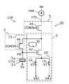
- FIG. 1A is a diagram schematically showing an exemplary circuit configuration of the image pickup apparatus according to the first embodiment.
- FIG. 1B is a diagram schematically showing an exemplary circuit configuration of pixels of the image pickup apparatus according to the first embodiment.
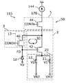
- FIG. 1C is a diagram schematically showing another exemplary circuit configuration of pixels of the image pickup apparatus according to the first embodiment.
- FIG. 2 is a cross-sectional view schematically showing the device structure of the pixels of the image pickup apparatus according to the first embodiment.
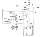
- FIG. 3 is a diagram schematically showing another exemplary circuit configuration of pixels of the image pickup apparatus according to the first embodiment.
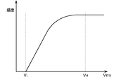
- FIG. 4 is a diagram showing an example of photoelectric conversion characteristics of the organic photoelectric conversion film.
- FIG. 5A is a timing chart for explaining an example of the operation in the image pickup apparatus according to the comparative example.
- FIG. 5B is a flowchart showing an example of the operation in the image pickup apparatus according to the comparative example.
- FIG. 5C is a flowchart showing another example of the operation in the image pickup apparatus according to the comparative example.
- FIG. 6A is a timing chart for explaining an example of the operation in the image pickup apparatus according to the first embodiment.
- FIG. 6B is a flowchart showing an example of the operation in the image pickup apparatus according to the first embodiment.
- FIG. 6C is a timing chart for explaining another example of the operation in the image pickup apparatus according to the first embodiment.
- FIG. 6D is a flowchart showing another example of the operation in the image pickup apparatus according to the first embodiment.
- FIG. 7 is a flowchart showing still another example of the operation in the image pickup apparatus according to the first embodiment.
- FIG. 8 is a schematic view showing an example of the configuration of the image pickup apparatus according to the second embodiment.
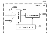
- FIG. 9 is a block diagram showing an example of the configuration of the camera system according to the third embodiment.
- a sensor using a photoelectric conversion film such as an organic CMOS sensor cannot completely transfer signal charges because the PD portion and the semiconductor layer are electrically connected by metal wiring. Therefore, in general, an incomplete transfer noise and an afterimage are prevented from occurring by having a structure in which the PD unit and the FD unit are electrically connected to read out the signal charge of the PD unit.
- the signal voltage of the FD section is read out with the voltage changed by the electric charge accumulated during the exposure detected by the FD section, and then the reset voltage is read out with the FD section reset, and the signal voltage is read. And the difference between the reset voltage and the reset voltage will be acquired.
- the reset noise cannot be removed, and the random noise is larger than the reading using the CDS technology described above. There is a problem.
- the CDS technology is an effective technology for suppressing reset noise, it brings about an increase in manufacturing cost due to the complicated process, and further, a CMOS type solid-state image sensor having a structure effective in terms of function and performance. There is a problem that it cannot be applied to.
- the exposure is started by the trigger signal from the outside, especially in the specifications of industrial cameras, commercial broadcasting cameras, medical cameras, etc., and in particular, at least two pixels or more are simultaneously exposed.
- a command signal for starting exposure or starting surface batch exposure is input, it takes time to remove the reset noise of each pixel row by row before exposure.
- the trigger signal is, for example, a signal emitted in accordance with the operation of another machine, or a signal emitted when a person presses a shutter button or the like.
- the solid-state image sensor disclosed in Patent Document 5 is configured to enable high-speed exposure start by providing two trigger signals in advance, but signal control becomes complicated.
- an object of the present disclosure to provide an image pickup device provided with a solid-state image pickup device capable of appropriately removing reset noise and starting exposure to a trigger signal from the outside at high speed.
- the imaging apparatus includes a photoelectric conversion unit that converts light into a signal charge and a charge storage unit that stores the signal charge, and controls a plurality of pixels arranged in a matrix.
- the control circuit includes a circuit, and the control circuit performs a reset operation for initializing the potential of the charge storage unit to a pixel belonging to at least one row among the plurality of pixels before receiving a trigger signal instructing the start of exposure.
- the signal charge is stored in the charge storage unit without causing the pixel belonging to at least one of the plurality of pixels to perform the reset operation after receiving the trigger signal.
- the plurality of pixels are made to perform the exposure operation accumulated in the above at the same time.
- the control circuit After receiving the trigger signal, the control circuit causes a plurality of pixels belonging to at least one row to perform an exposure operation without performing a reset operation. Therefore, the time from the reception of the trigger signal to the exposure operation is shortened as compared with the case where the reset operation is executed for all the pixels after the reception of the trigger signal. Further, since the reset operation is performed on the pixels belonging to at least one row by the time the trigger signal is received, the potential is initialized before the signal charge is accumulated, and the reset operation is particularly performed while suppressing the reset noise. If so, the noise in the signal charge of the pixels belonging to at least one row is reduced. Therefore, the image pickup apparatus according to this aspect can reduce the time lag from the trigger signal instructing the start of exposure to the start of exposure while the noise is reduced.
- control circuit may cause all the pixels of the plurality of pixels to sequentially perform the reset operation line by line or line by line before receiving the trigger signal.
- the reset operation is performed on a plurality of pixels belonging to all the rows by the time the trigger signal is received, the potential is initialized before the signal charge is accumulated, and the reset operation is performed in particular while suppressing the reset noise. If so, the noise in the signal charges of all the plurality of pixels is reduced.
- control circuit may cause a pixel belonging to at least one row of the plurality of pixels to perform the reset operation a plurality of times before receiving the trigger signal.
- the pixels belonging to at least one row are reset multiple times before the control circuit receives the trigger signal. Therefore, in the pixel that performs the reset operation a plurality of times, after the reset operation is performed once, the charge accumulated in the charge storage unit due to the dark current or the like is initialized again by the reset operation. Therefore, the noise caused by the accumulated charge due to the dark current or the like is reduced, so that the image pickup apparatus according to this embodiment can further reduce the noise.
- control circuit may cause the plurality of pixels to repeatedly perform the reset operation line by line or line by line until the trigger signal is received.
- the reset operation is repeatedly performed on a plurality of pixels until the control circuit receives the trigger signal. Therefore, after the reset operation is performed, the charges accumulated in the charge storage unit due to the dark current or the like are repeatedly initialized by the reset operation. Therefore, the noise caused by the accumulated charge due to the dark current or the like is reduced, so that the image pickup apparatus according to this embodiment can further reduce the noise.
- control circuit performs a read operation for outputting a signal corresponding to the signal charge accumulated in the charge storage unit after the exposure operation in units of lines or a plurality of lines from the line in which the reset operation is started.
- the plurality of pixels may be subjected to the operation in order in units.
- the line at which the reset operation and the read operation are started is shared, so that the complexity of the control circuit can be suppressed. Further, since the read data is continuously read in time from the ascending line to the descending line or from the descending line to the ascending line, the continuity of the obtained image is maintained.
- control circuit causes the plurality of pixels to sequentially perform the reset operation up to a line different from the line in which the reset operation is started in units of rows or in units of a plurality of rows, and after the exposure operation, the charge is charged.
- a read operation for outputting a signal corresponding to the signal charge accumulated in the storage unit is performed on the plurality of pixels in order from the line next to the line in which the reset operation is completed, line by line or in units of a plurality of lines. May be good.
- each of the plurality of pixels may include a feedback circuit that negatively feeds back the potential of the charge storage unit in the reset operation.
- the image pickup apparatus can further reduce noise.
- each of the plurality of pixels may include a circuit that suppresses reset noise generated in the reset operation.
- the image pickup apparatus can further reduce noise.
- a voltage supply circuit is further provided, and the photoelectric conversion unit includes a counter electrode electrically connected to the voltage supply circuit, a pixel electrode electrically connected to the charge storage unit, and the counter electrode.
- the control circuit includes a photoelectric conversion layer located between the electrode and the pixel electrode, and the control circuit applies a voltage to the counter electrode to the voltage supply circuit to form an electric field in the photoelectric conversion layer.
- the exposure operation may be performed on the plurality of pixels.
- control method includes a photoelectric conversion unit that converts light into a signal charge and a charge storage unit that stores the signal charge, and includes a plurality of pixels arranged in a matrix. It is a control method of the imaging device provided, and a reset operation for initializing the potential of the charge storage unit is performed on a pixel belonging to at least one row among the plurality of pixels before receiving a trigger signal instructing the start of exposure.
- the signal charge is stored in the charge storage unit without performing the reset operation on the pixel belonging to at least one of the plurality of pixels after receiving the trigger signal in a row-by-line or a plurality of row-by-line order.
- the exposure operation is performed on the plurality of pixels at the same time.
- the control method can reduce the time lag from the trigger signal instructing the start of exposure to the start of exposure while reducing noise.
- each drawing is just a diagram showing a concept, and the scale, shape, etc. are not taken into consideration at all. Therefore, for example, the scales and the like do not always match in each figure. Further, in each figure, substantially the same configuration is designated by the same reference numerals, and duplicate description will be omitted or simplified.
- the terms “upper” and “lower” do not refer to the upward direction (vertically upward) and the downward direction (vertically downward) in absolute spatial recognition, but are based on the stacking order in the stacking configuration. It is used as a term defined by the relative positional relationship with. Also, the terms “upper” and “lower” are used not only when the two components are spaced apart from each other and another component exists between the two components, but also when the two components It also applies when the two components are placed in close contact with each other and touch each other.
- FIG. 1A is a diagram schematically showing an exemplary circuit configuration of the image pickup apparatus 100 according to the present embodiment.
- the image pickup device 100 is, for example, a laminated image pickup device, and has a photoelectric conversion layer laminated on a semiconductor substrate.
- the image pickup apparatus 100 includes a plurality of pixels 110 and peripheral circuits.
- the peripheral circuit includes a control circuit that controls the operation of the plurality of pixels 110.
- the control circuit receives a trigger signal from the outside and causes a plurality of pixels 110 to perform an exposure operation.
- the plurality of pixels 110 are arranged two-dimensionally to form a photosensitive region, so-called pixel region.
- the plurality of pixels 110 may be arranged one-dimensionally.
- the image pickup apparatus 100 is a line sensor.
- the plurality of pixels 110 are arranged in the row direction and the column direction.
- the row direction and the column direction mean the directions in which the rows and columns extend, respectively. That is, the vertical direction is the column direction and the horizontal direction is the row direction.
- Each of the pixels 110 is connected to the power supply line 120.
- a predetermined power supply voltage is supplied to each pixel 110 via the power supply line 120.
- the image pickup apparatus 100 has a storage control line 130 that applies the same constant voltage to all the photoelectric conversion layers that photoelectrically convert the incident light. However, when performing different control such as suppressing fluctuation, the voltage may be applied by dividing it into several parts.
- the peripheral circuit includes a voltage supply circuit 140, a vertical scanning circuit 141, a column signal processing circuit 142, a horizontal signal readout circuit 143, and a constant current source 144.
- the vertical scanning circuit 141 is also referred to as a "row scanning circuit”
- the horizontal signal readout circuit 143 is also referred to as a "column scanning circuit”.
- the column signal processing circuit 142 and the constant current source 144 may be arranged for each row of pixels 110 arranged in two dimensions.
- the voltage supply circuit 140 is connected to the storage control line 130. During operation of the image pickup apparatus 100, a predetermined bias voltage is applied to the counter electrode 1b (details will be described later) of the pixel 110 via the storage control line 130 by the voltage supply circuit 140. The operation of the voltage supply circuit 140 is controlled by the control circuit.
- the vertical scanning circuit 141 is connected to the selection control signal line CON7 and the amplification control signal line CON3.
- the amplification control signal line CON3 is also referred to as a "bandwidth control signal line”
- the selection control signal line CON7 is also referred to as an "address signal line”.
- the vertical scanning circuit 141 is a part of a control circuit that controls the operation of the plurality of pixels 110.
- the vertical scanning circuit 141 selects a plurality of pixels 110 arranged in each row in units of rows by applying a predetermined voltage to the selection control signal line CON7. As a result, the reading of the signal voltage of the selected pixel 110 and the reset of the pixel electrode described later are executed.
- the pixels 110 arranged in each row are electrically connected to the column signal processing circuit 142 via the signal readout signal line 170 corresponding to each row.
- the signal readout signal line 170 is also referred to as a "vertical signal line”.
- the column signal processing circuit 142 performs noise suppression signal processing represented by correlated double sampling, analog-to-digital conversion (AD conversion), and the like.
- a horizontal signal reading circuit 143 is electrically connected to a plurality of column signal processing circuits 142 provided corresponding to a row of pixels 110A. The horizontal signal reading circuit 143 sequentially reads signals from the plurality of column signal processing circuits 142 to the horizontal common signal line 180.
- FIG. 1B is a diagram schematically showing an exemplary circuit configuration of pixels 110 of the image pickup apparatus 100 according to the present embodiment.
- the pixel 110 includes a photoelectric conversion unit 1, an amplifier 2, a band control unit 3, a charge storage unit FD, and an output selection unit 5.
- the photoelectric conversion unit 1 detects light and converts the light into a signal charge.
- the charge storage unit FD stores the signal charge generated by the photoelectric conversion unit 1.
- the readout circuit 50 is formed by the amplifier 2, the band control unit 3, the charge storage unit FD, and the output selection unit 5.
- the photoelectric conversion unit 1 converts light into a signal charge.
- the read-out circuit 50 reads out the signal charge generated by the photoelectric conversion unit 1.
- the photoelectric conversion unit 1 includes, for example, a pixel electrode 1a, a counter electrode 1b, and a photoelectric conversion layer 1c sandwiched between the pixel electrode 1a and the counter electrode 1b.
- the pixel electrode 1a is electrically connected to the charge storage unit FD.
- the counter electrode 1b is connected to the storage control line 130 shown in FIG. 1A, and is electrically connected to the voltage supply circuit 140 via the storage control line 130.
- the signal charge generated by the photoelectric conversion layer 1c of the photoelectric conversion unit 1 is charged. It can be stored in the storage unit FD.
- the charge storage unit FD is connected to the photoelectric conversion unit 1 by a wiring layer.
- the charge storage unit FD stores the signal charge generated by the photoelectric conversion unit 1.
- the charge storage unit FD is further connected to the input of the amplifier 2.
- the amplifier 2 amplifies the signal corresponding to the signal charge accumulated in the charge storage unit FD, and outputs the signal to the band control unit 3 and the output selection unit 5.
- the amplifier 2 and the band control unit 3 form a feedback circuit 30 via the charge storage unit FD.
- the band control unit 3 includes a band control circuit 13.
- the band control circuit 13 is supplied with at least three different voltages from the voltage control circuit. By supplying such a voltage, the band control circuit 13 has a band control function.
- the voltage control circuit is, for example, a part of the vertical scanning circuit 141.
- the band control circuit 13 limits the output signal of the amplifier 2 and outputs it to the charge storage unit FD.
- the signal read from the charge storage unit FD is amplified by the amplifier 2, band-limited by the band control circuit 13, and returned to the charge storage unit FD.
- the feedback circuit 30 negatively feeds back the signal of the photoelectric conversion unit 1 to the charge storage unit FD via the amplification transistor 42.
- the feedback circuit 30 is a circuit that negatively feeds back the potential of the charge storage unit FD in the reset operation described later.
- the amplifier 2 has an amplification transistor 42 and a switching circuit 20 including a first switch element 11 and a second switch element 12.
- the transistor in the read circuit 50 is, for example, an N-channel MOSFET (Metal Oxide Semiconductor Field Effect Transistor).
- MOSFET Metal Oxide Semiconductor Field Effect Transistor
- the charge storage unit FD is connected to the gate of the amplification transistor 42.
- the band control unit 3 includes a band control transistor 46.
- the output selection unit 5 includes a selection transistor 44.
- One of the source and drain of the amplification transistor 42 is connected to one of the source and drain of the bandwidth control transistor 46 and one of the source and drain of the selection transistor 44. Further, the other of the source and drain of the band control transistor 46 is connected to the charge storage unit FD.
- the RC filter circuit is formed by the band control transistor 46 and the capacitance component parasitic on the charge storage unit FD.
- the amplification control signal line CON3 is connected to the gate of the band control transistor 46.
- the state of the band control transistor 46 is determined by the voltage of the amplification control signal line CON3. For example, when the voltage of the amplification control signal line CON3 is high, the band control transistor 46 is turned on. As a result, a feedback path is formed by the charge storage unit FD, the amplification transistor 42, and the band control transistor 46.
- the other of the source and drain of the selection transistor 44 is connected to the signal read signal line 170.
- the gate of the selection transistor 44 is controlled by the selection control signal line CON7.
- the state of the selection transistor 44 is determined by the voltage of the selection control signal line CON7. For example, when the voltage of the selection control signal line CON7 is at a high level, the selection transistor 44 is turned on. As a result, the amplification transistor 42 and the signal readout signal line 170 are electrically connected. When the voltage of the selection control signal line CON7 is low level, the selection transistor 44 is turned off. As a result, the amplification transistor 42 and the signal readout signal line 170 are electrically separated.
- a switching circuit 20 is connected to the other of the source and drain of the amplification transistor 42.
- the other of the source and drain of the amplification transistor 42 is connected to the first voltage source VA1 via the first switch element 11. Further, the other of the source and drain of the amplification transistor 42 is also connected to the second voltage source VA2 via the second switch element 12.
- the switching circuit 20 By controlling the switching circuit 20 with the control signals V1 and V2, the voltage applied to the other of the source and drain of the amplification transistor 42 is switched to the voltage Va1 or the voltage Va2.
- the voltage Va1 of the first voltage source VA1 is, for example, the ground voltage GND.
- the voltage Va2 of the second voltage source VA2 is, for example, the power supply voltage VDD.
- the switching circuit 20 may be provided for each pixel, or may be shared by a plurality of pixels in order to reduce the number of elements per pixel.
- the output selection unit 5 is connected to the signal read signal line 170.
- the signal readout signal line 170 is shared by at least two pixels.
- the signal amplified by the amplifier 2 is output to the signal read signal line 170 via the output selection unit 5.
- a constant current source 144 is connected to the signal readout signal line 170.
- the selection transistor 44 When the selection transistor 44 is on, the selection transistor 44, the amplification transistor 42, and the constant current source 144 form a source follower circuit.
- the signal corresponding to the signal charge accumulated in the charge storage unit FD is output to the signal read signal line 170 and read to the outside.
- the constant current source 144 may be provided for each pixel, or may be shared by a plurality of pixels in order to reduce the number of elements per pixel.
- the photoelectric conversion unit 1 is not limited to such a configuration, and may be an element having another photoelectric conversion function such as a photodiode.
- FIG. 1C is a diagram schematically showing an exemplary circuit configuration of pixels 115 of the image pickup apparatus according to the present embodiment.
- the pixel 115 shown in FIG. 1C is different from the pixel 110 described above in that it includes a photoelectric conversion unit 1d instead of the photoelectric conversion unit 1.
- the configuration of the pixel 115 other than the photoelectric conversion unit 1d is the same as that of the pixel 110.
- the pixel 115 includes a photoelectric conversion unit 1d composed of a photodiode.
- the signal charge generated by the photoelectric conversion unit 1d is generated by applying a reference voltage Vp to one end of the photoelectric conversion unit 1d and connecting one end of the node forming the charge storage unit FD to the other end of the photoelectric conversion unit 1d. Can be stored in the charge storage unit FD.
- FIG. 2 is a cross-sectional view schematically showing the device structure of the pixel 110 of the image pickup apparatus 100 according to the present embodiment.
- the pixel 110 includes a semiconductor substrate 62 that supports the photoelectric conversion unit 1.
- the semiconductor substrate 62 is, for example, a silicon substrate.
- the photoelectric conversion unit 1 is arranged above the semiconductor substrate 62.
- the interlayer insulating layers 63A, 63B and 63C are laminated on the semiconductor substrate 62, and the laminated body of the pixel electrode 1a, the photoelectric conversion layer 1c and the counter electrode 1b is arranged on the interlayer insulating layer 63C. ..
- the pixel electrode 1a is partitioned for each pixel, and the pixel electrode 1a is spatially separated and formed between two adjacent pixels 110, so that the two adjacent pixel electrodes 1a are electrically separated. ing. Further, the photoelectric conversion layer 1c and the counter electrode 1b may be formed so as to straddle a plurality of pixels 110.
- the signal charge generated by the photoelectric conversion unit 1 is stored in the charge storage node 41 between the gate of the amplification transistor 42 and the photoelectric conversion unit 1.
- the charge storage node 41 is an example of the above-mentioned charge storage unit FD.
- the photoelectric conversion unit 1 includes, for example, a pixel electrode 1a, a counter electrode 1b facing the pixel electrode 1a, and a photoelectric conversion layer 1c located between the pixel electrode 1a and the counter electrode 1b. including.
- the pixel electrode 1a is an electrode for reading out the signal charge generated by the photoelectric conversion unit 1. There is at least one pixel electrode 1a for each pixel 110. The pixel electrode 1a is electrically connected to the gate electrode 42e of the amplification transistor 42 and the impurity region 62d.
- the pixel electrode 1a is formed by using a conductive material.
- the conductive material is, for example, a metal such as aluminum or copper, a metal nitride, or polysilicon to which conductivity is imparted by doping with impurities.
- the counter electrode 1b is, for example, a transparent electrode formed of a transparent conductive material.
- the counter electrode 1b is arranged on the side where light is incident in the photoelectric conversion unit 1. Therefore, the light transmitted through the counter electrode 1b is incident on the photoelectric conversion layer 1c.
- transparent in the present specification means that at least a part of light in the wavelength range to be detected is transmitted, and it is not essential to transmit light over the entire wavelength range of visible light.
- the counter electrode 1b is formed by using, for example, a transparent conductive oxide (TCO: Total Cost of Manufacturing Oxide) such as ITO (Indium Tin Oxide).
- TCO Total Cost of Manufacturing Oxide
- ITO Indium Tin Oxide
- the photoelectric conversion layer 1c receives the incident light to generate a hole-electron pair.
- a semiconductor inorganic material, a semiconductor organic material, or the like is used as the material of the photoelectric conversion layer 1c.
- the photoelectric conversion layer 1c is, for example, an organic photoelectric conversion film.
- An amplification transistor 42, a selection transistor 44, and a band control transistor 46 are formed on the semiconductor substrate 62.
- the amplification transistor 42 includes impurity regions 62a and 62b formed on the semiconductor substrate 62, a gate insulating layer 42g located on the semiconductor substrate 62, and a gate electrode 42e located on the gate insulating layer 42g.
- the impurity regions 62a and 62b function as drains or sources of the amplification transistor 42.
- the impurity regions 62a and 62b and the impurity regions 62c, 62d and 62e described later are, for example, n-type impurity regions.
- the selection transistor 44 includes impurity regions 62a and 62c formed on the semiconductor substrate 62, a gate insulating layer 44g located on the semiconductor substrate 62, and a gate electrode 44e located on the gate insulating layer 44g. Impurity regions 62a and 62c serve as drains or sources for the selection transistor 44.
- the amplification transistor 42 and the selection transistor 44 share the impurity region 62a, so that the source (or drain) of the amplification transistor 42 and the drain (or source) of the selection transistor 44 are electrically connected. There is.
- the band control transistor 46 includes impurity regions 62d and 62e formed in the semiconductor substrate 62, a gate insulating layer 46g located on the semiconductor substrate 62, and a gate electrode 46e located on the gate insulating layer 46g.
- the impurity regions 62d and 62e function as drains or sources of the band control transistor 46.
- an element separation region 62s is provided between the pixels 110 adjacent to each other and between the amplification transistor 42 and the band control transistor 46. Pixels 110 adjacent to each other are electrically separated by the element separation region 62s. Further, by providing the element separation region 62s between the pixels 110 adjacent to each other, leakage of the signal charge accumulated in the charge storage node 41 is suppressed.
- a contact plug 65A connected to the impurity region 62d of the band control transistor 46, a contact plug 65B connected to the gate electrode 42e of the amplification transistor 42, and a contact plug 65A and a contact plug 65B are provided in the interlayer insulating layer 63A.
- the wiring 66A to be connected is formed.
- the impurity region 62d (for example, drain) of the band control transistor 46 is electrically connected to the gate electrode 42e of the amplification transistor 42.
- the plug 67A and the wiring 68A are further formed in the interlayer insulating layer 63A.
- the plug 67B and the wiring 68B are formed in the interlayer insulating layer 63B, and the plug 67C is formed in the interlayer insulating layer 63C, so that the wiring 66A and the pixel electrode 1a are electrically connected.
- the contact plug 65A, the contact plug 65B, the wiring 66A, the plug 67A, the wiring 68A, the plug 67B, the wiring 68B, and the plug 67C are typically made of metal.
- the color filter 72 is arranged on the counter electrode 1b. Further, the microlens 74 is arranged on the color filter 72. Although not shown, a protective layer for protecting the photoelectric conversion unit 1 may be arranged between the color filter 72 and the microlens 74.
- the material of the protective layer is, for example, SiON or AlO.
- the image pickup apparatus 100 as described above can be manufactured by using a general semiconductor manufacturing process.
- a silicon substrate is used as the semiconductor substrate 62, it can be manufactured by using various silicon semiconductor processes.
- the photoelectric conversion operation will be described.
- the light input from the outside is collected by the microlens 74 of each pixel 110, passes through only the desired wavelength by the color filter 72, and is incident on the photoelectric conversion unit 1.
- the photoelectric conversion unit 1 converts light into electric charges.
- the converted charge is collected by the pixel electrode 1a and stored in the charge storage node 41, in other words, the charge storage unit FD. Will be done.
- FIG. 3 is a diagram schematically showing an exemplary circuit configuration of the pixel 110A of the image pickup apparatus according to the present embodiment.
- the pixel 110A shown in FIG. 3 is different from the pixel 110 described above in that it includes a band control unit 3A instead of the band control unit 3.
- the differences from the pixel 110 will be mainly described, and the description of the common points will be omitted or simplified.
- the readout circuit 50A is formed by the amplifier 2, the band control unit 3A, the charge storage unit FD, and the output selection unit 5.
- the feedback circuit 30A negatively feeds back the signal from the photoelectric conversion unit 1 to the charge storage unit FD via the amplification transistor 42.
- the feedback circuit 30A is a circuit that negatively feeds back the potential of the charge storage unit FD in the reset operation described later.
- the band control unit 3A includes a band control circuit 13A and a reset circuit 14A.
- the band control circuit 13A is a circuit that suppresses reset noise generated in the reset operation described later.
- the band control circuit 13A includes a band control transistor 46A, a first capacitive element 9, and a second capacitive element 10.
- the "capacitive element” means a structure in which a dielectric material such as an insulating film is sandwiched between electrodes.
- the “electrode” is not limited to an electrode formed of a metal, and is interpreted to include a polysilicon layer and the like widely. The electrode may be a part of the semiconductor substrate.
- the first capacitive element 9 and the second capacitive element 10 may be, for example, a MIM (Metal Insulator Metal) capacitance or a MIS (Metal Insulator Semiconductor) capacitance.
- the reset circuit 14A includes a reset transistor 48.
- the gate of the amplification transistor 42 is connected to the charge storage unit FD.
- One of the source and drain of the amplification transistor 42 is connected to one of the source and drain of the bandwidth control transistor 46A.
- One of the source and drain of the amplification transistor 42 is also connected to one of the source and drain of the selection transistor 44.
- the other of the source and drain of the band control transistor 46A is connected to one end of the first capacitive element 9.
- a reference voltage VR1 is applied to the other end of the first capacitance element 9.
- the RC filter circuit is formed by the band control transistor 46A and the first capacitive element 9.
- the other of the source and drain of the band control transistor 46A is also connected to one end of the second capacitive element 10. Further, the other end of the second capacitance element 10 is connected to the charge storage unit FD.
- the node formed between the bandwidth control transistor 46A, the first capacitive element 9 and the second capacitive element 10 is referred to as “RD”.
- the gate of the band control transistor 46A is connected to the amplification control signal line CON3.
- the state of the band control transistor 46A is determined by the voltage of the amplification control signal line CON3. For example, when the voltage of the amplification control signal line CON3 is high, the band control transistor 46A is turned on. At this time, the feedback circuit 30A is formed by the charge storage unit FD, the amplification transistor 42, the band control transistor 46A, and the second capacitive element 10.
- the resistance component of the band control transistor 46A becomes large. Therefore, the band of the band control transistor 46A is narrowed, and the frequency domain of the feedback signal is narrowed.
- the signal output by the band control transistor 46A is attenuated by the attenuation circuit formed by the parasitic capacitance of the second capacitance element 10 and the charge storage section FD, and returns to the charge storage section FD. Will be done. Assuming that the capacitance of the second capacitance element 10 is Cc and the parasitic capacitance of the charge storage unit FD is Cfd, the attenuation factor is represented by Cc / (Cc + Cfd).
- the charge storage unit FD is further connected to one of the source and drain of the reset transistor 48.
- the other of the source and drain of the reset transistor 48 is connected to the RD.
- one of the source and drain voltages of the amplification transistor 42 (output voltage of the amplifier 2) is applied to the reset transistor 48.
- the gate of the reset transistor 48 is connected to the reset control signal line CON2, and the state of the reset transistor 48 is determined by the voltage of the reset control signal line CON2.
- the reset transistor 48 negatively feeds the signal of the photoelectric conversion unit 1 to the charge storage unit FD via the amplification transistor 42. According to such a configuration, it is possible to reduce the change in the voltage of the charge storage unit FD before and after turning off the reset transistor 48, and it is possible to suppress noise at a higher speed.
- the control circuit of the image pickup apparatus 100 has an exposure operation for accumulating signal charges in the charge storage unit FD in a plurality of pixels 110, a reset operation for initializing the potential of the charge storage unit FD, and storage in the charge storage unit FD.
- a read operation is performed to output a signal corresponding to the signal charge.
- the control circuit causes a plurality of pixels 110 to perform an exposure operation by the following operations.
- FIG. 4 is a diagram showing an example of the photoelectric conversion characteristics of the organic photoelectric conversion film as an example of the characteristics of the photoelectric conversion layer 1c.
- the photoelectric conversion characteristics of the organic photoelectric conversion film the higher the voltage V ITO of the counter electrode 1b, the higher the sensitivity of the organic photoelectric conversion film.
- the HIGH voltage is supplied to the counter electrode 1b common to all pixels in a state where the pixel electrode 1a provided in each pixel 110 is set to the reset voltage VRST, the counter electrode 1b and the pixel electrode 1a are high. Since the voltage VH is applied, the sensitivity of the organic photoelectric conversion film is high, and photoelectric conversion is performed.
- the signal charge generated in the photoelectric conversion layer 1c is collected by the pixel electrode 1a.
- the voltage applied to the counter electrode 1b and the pixel electrode 1a is changed to a low voltage VL , so that the sensitivity of the organic photoelectric conversion film becomes low and the photoelectric conversion is stopped.
- the exposure operation is started by supplying the HIGH voltage to the counter electrode 1b common to all pixels, and the facing electrode 1b is LOW.
- the exposure operation is stopped by the supply of voltage.
- the band control transistor 46 is off.
- the voltages of the reset control signal line CON2 and the amplification control signal line CON3 shown in FIG. 2 are at a low level, and the band control transistor 46A and the reset transistor 48 are off.
- the signal charge is accumulated in the charge storage unit FD during the exposure operation.
- the photoelectric conversion characteristic that is, the sensitivity
- the photoelectric conversion characteristic can be controlled by controlling the voltage applied to the counter electrode 1b.
- by using such control of photoelectric conversion characteristics that is, sensitivity characteristics
- the CDS method cannot be used because the charge cannot be completely transferred. Therefore, it is essential to suppress reset noise (for example, kTC noise) for each pixel before exposure. Even before the start of the global shutter exposure described above, a reset operation is required for the pixels to be exposed.
- reset noise for example, kTC noise
- the control circuit causes a plurality of pixels 110 to perform a reset operation by the following operations.
- the reset operation is performed in units of rows of the plurality of pixels 110.
- the potential of the charge storage unit FD is initialized while suppressing the reset noise.
- the voltage of the selection control signal line CON7 is at a low level. Therefore, the selection transistor 44 is in the off state, and the amplification transistor 42 and the signal readout signal line 170 are electrically separated.
- the voltage of the amplification control signal line CON3 is set to a high level, and the band control transistor 46 is turned on.
- the first switch element 11 of the switching circuit 20 is in the ON state, and the voltage Va1 (for example, the ground voltage GND) is applied to the other of the source and drain of the amplification transistor 42.
- the voltage of the charge storage unit FD in other words, the voltage of the pixel electrode 1a
- the voltage of the charge storage unit FD becomes equal to the reset voltage VRST.
- the potential of the charge storage unit FD is initialized. Further, for example, the voltage of the amplification control signal line CON3 is then set to a voltage between the high level and the low level, for example, an intermediate voltage. As a result, reset noise is suppressed. In this case, if the voltage is set so that the operating band of the band control transistor 46 is narrower than the operating band of the amplification transistor 42, the reset noise suppression effect is further enhanced. Finally, the voltage of the amplification control signal line CON3 is lowered and the band control transistor 46 is turned off. As a result, the reset noise is suppressed and the potential of the charge storage unit FD is initialized.
- the voltage of the reset control signal line CON2 is raised to a high level and the reset transistor 48 is turned on to accumulate charge.
- the voltage of the part FD becomes equal to the reset voltage VRST.
- the reset transistor 48 is turned off.
- the voltages of the reset control signal line CON2 and the amplification control signal line CON3 are lowered to a low level, and the band control transistor 46A is turned off.
- the control circuit causes a plurality of pixels 110 to perform a read operation by the following operations.
- the reading operation is performed in units of rows of a plurality of pixels 110.
- the voltage of the selection control signal line CON7 is set to a high level and the selection transistor 44 is turned on. Further, the switching circuit 20 is controlled so that the other voltage of the source and drain of the amplification transistor 42 becomes Va2 (for example, the power supply voltage VDD). That is, the second switch element 12 is turned on, and the voltage Va2 is applied to the other of the source and drain of the amplification transistor 42. In this state, the amplification transistor 42 and the constant current source 144 form a source follower circuit. Then, the potential of the charge storage unit FD becomes a voltage corresponding to the amount of the signal charge stored in the charge storage unit FD.
- Va2 for example, the power supply voltage VDD
- the voltage of the charge storage unit FD according to the amount of signal charge is amplified by the amplifier 2 at an amplification factor of, for example, about 1 time, and is output to the signal read signal line 170.
- the amplification factor of the source follower circuit is, for example, about 1 time.
- the voltage of the charge storage unit FD is amplified by the amplifier 2 at an amplification factor of, for example, about 1 times, and is output to the signal readout signal line 170.
- This read operation is performed in a state in which the signal charge in the exposure operation is accumulated in the charge storage unit FD, and in a state in which the reset operation for the pixels is completed and the reset voltage VRST is set in the pixel electrodes.
- the read operation in the state where the signal charge in the exposure operation is accumulated in the charge storage unit FD is called “signal read operation”
- the read operation in the state where the reset voltage VRST is set in the pixel electrode is called “reset signal”. It is called "reading operation”.
- the imaging apparatus according to the comparative example will be described with reference to FIGS. 5A, 5B, and 5C.
- the image pickup apparatus according to the comparative example has the same configuration as the image pickup apparatus 100 described above, but the operation by each circuit is different from that of the image pickup apparatus 100 according to the present embodiment.
- a plurality of pixels 110 of the image pickup apparatus according to the comparative example form a pixel array of “0 rows to n rows ⁇ 0 columns to m columns” will be described.
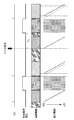
- FIG. 5A is a timing chart for explaining an example of the operation in the image pickup apparatus according to the comparative example.
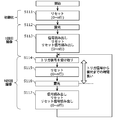
- FIG. 5B is a flowchart showing an example of the operation in the image pickup apparatus according to the comparative example.
- FIG. 5A shows the timing of the trigger signal, the timing of the falling (or rising) of the vertical synchronization signal VD, and the voltage applied to the counter electrode 1b of the photoelectric conversion unit 1 (that is, the bias applied to the photoelectric conversion layer 1c). It shows a temporal change in the magnitude of the voltage), driving the entire plurality of pixels 110, and resetting operation, signal reading operation, and exposure operation in each row of the pixel array of the plurality of pixels 110.
- the timing of the "trigger signal” instructing the start of exposure is shown.
- “VD” in the uppermost graph in FIG. 5A indicates the timing of the falling (or rising) of the vertical synchronization signal VD.
- the “opposite electrode voltage” in the second graph from the top in FIG. 5A shows the temporal change of the voltage applied from the voltage supply circuit 140 to the counter electrode 1b via the storage control line 130.
- pixel drive and “each row operation” indicate the timing of driving the entire plurality of pixels 110 and the operation of each row of the pixel array of the plurality of pixels 110, respectively.
- the line of each line operation indicates that the operation is sequentially performed line by line from the 0th line to the nth line.
- the solid line of each line operation indicates the reset operation, and the broken line indicates the signal read operation.
- a reset operation is performed on the plurality of pixels 110 of all the rows from 0 to n at least for each row (S111).
- the reset operation is performed, for example, as described above, the reset operation is performed together with suppressing the reset noise (for example, kTC noise).
- the HIGH voltage is applied to the counter electrode 1b during the exposure operation period B in a state where the reset noise of all the pixels 110 is suppressed and the reset voltage VRST is set.
- a plurality of pixels 110 are made to perform an exposure operation (S112). The exposure operation is collectively performed on the pixels 110 having at least two or more pixels among the plurality of pixels 110.
- the control circuit of the image pickup apparatus performs a signal reading operation for at least one row for the pixels 110 belonging to all the rows from 0 to n in the signal reading operation period C after the exposure operation.
- the reset operation for all the pixels 110 that read the signal and the reset signal read operation for all the pixels 110 after the reset operation are performed again (S113).
- the reset signal read operation the noise of all the pixels 110 that read the signal is suppressed, and the reset signal read operation is performed at least line by line with the reset voltage VRST set.
- the control circuit of the image pickup apparatus receives a trigger signal from the outside, determines the exposure start time, and causes the plurality of pixels 110 to perform the reset operation, the exposure operation, and the signal reading operation (S114 to S117). .. In steps S115 to S117, the same operations as in steps S111 to S113 are performed. At this time, after receiving the trigger signal in step S114 and before the exposure operation in step 116, a reset operation for 110 minutes of all the pixels to be exposed is required at least for each line, and the trigger signal is received from the outside. , A long waiting time T1 occurs before the start of the exposure operation.
- FIG. 5C is a flowchart showing another example of the operation in the image pickup apparatus according to the comparative example.
- the control circuit of the image pickup apparatus according to the comparative example first receives a trigger signal from the outside, and causes a plurality of pixels 110 to perform a reset operation, an exposure operation, and a signal reading operation (S121 to S124). ).
- steps S121 to S124 the same operations as in steps S114 to S117 described above are performed.
- the imaging apparatus according to the comparative example determines the exposure operation start time in accordance with the reception of the trigger signal from the outside after performing the first imaging for initialization.
- the exposure operation start time may be determined according to the reception of the trigger signal from the outside from the beginning.
- the image pickup apparatus according to the comparative example may repeat the control of the exposure operation timing by the trigger signal from the outside and the continuous scanning inside.
- the image pickup apparatus 100 may include pixels 110A or pixels 115 instead of pixels 110.
- FIG. 6A is a timing chart for explaining an example of the operation of the image pickup apparatus 100 according to the present embodiment.
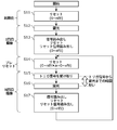
- FIG. 6B is a flowchart showing an example of the operation of the image pickup apparatus 100 according to the present embodiment.
- FIG. 6C is a timing chart for explaining another example of the operation of the image pickup apparatus 100 according to the present embodiment.
- 6A and 6C show the timing of the trigger signal, the timing of the falling (or rising) of the vertical synchronization signal VD, and the voltage applied to the counter electrode 1b of the photoelectric conversion unit 1 (that is, that is, in the same manner as in FIG. 5A.
- the control circuit of the image pickup apparatus 100 changes from row 0 to n in the reset operation period A.
- a reset operation is performed on the plurality of pixels 110 in all the rows (S11).
- the reset operation is performed, for example, as described above, the reset operation is performed at least for each line while suppressing the reset noise (kTC noise).
- the control circuit of the image pickup apparatus 100 may cause the pixel 110 belonging to at least one row of the plurality of pixels 110 to sequentially perform the reset operation in line units. For example, when the image is taken in the cutout mode using a part of the pixels 110, the reset operation may be performed on the row of the pixels 110 to be used.
- the control circuit of the image pickup apparatus 100 applies a HIGH voltage to the counter electrode 1b during the exposure operation period B in a state where the reset noise of all the pixels 110 is suppressed and the reset voltage VRST is set, and the pixel 110 Is to perform an exposure operation (S12).
- the exposure operation is performed simultaneously on at least two or more pixels 110 among the plurality of pixels 110.
- the exposure operation may be performed on all the pixels 110 at the same time.
- the control circuit of the image pickup apparatus 100 includes a signal reading operation of pixel signals accumulated in the pixels 110 belonging to all the rows from 0 to n at least one row at a time during the signal reading operation period C after the exposure operation. After reading, the reset operation for all the pixels 110 that read the signal and the reset signal reading operation for all the pixels 110 after the reset operation are performed again (S13). In the reset signal read operation, the noise of all the pixels 110 that read the signal is suppressed, and the reset signal read operation is performed at least line by line with the reset voltage VRST set.
- an external trigger signal is provided by providing a period (pre-reset operation period A2) in which the reset operation is repeated at least for each line. It is possible to shorten the waiting time from the receipt of the signal to the start of the exposure operation.
- the control circuit of the image pickup apparatus 100 causes a plurality of pixels 110 to perform a reset operation at least line by line during the pre-reset operation period A2 (S14).
- the reset operation in step S14 is repeated in units of 0 to n lines until the control circuit receives a trigger signal from the outside (S15). That is, the control circuit of the image pickup apparatus 100 causes the plurality of pixels 110 to repeatedly perform the reset operation in order on a line-by-line basis until the trigger signal is received.
- step S15 the control circuit of the image pickup apparatus 100 performs an interrupt process when receiving a trigger signal from the outside, and stops the reset operation until the process of the pixel 110 in the x-row is completed.
- the reset operation in step S14 is repeated a times in units of lines 0 to n, and is further performed from line 0 to line x.
- a is an integer of 0 or more.
- Line x is any line between lines 0 and n.
- steps S13 to S15 the control circuit of the image pickup apparatus 100 performs a reset operation of initializing the potential of the charge storage unit FD before receiving the trigger signal instructing the start of exposure of the plurality of pixels 110. Have them all do it line by line.
- control circuit of the image pickup apparatus 100 causes the pixel 110 belonging to at least one row of the plurality of pixels 110 to perform the reset operation a plurality of times before receiving the trigger signal. As a result, the accumulation of signal charges due to dark current or the like that causes noise is suppressed until the control circuit receives the trigger signal from the outside.
- the control circuit of the image pickup apparatus 100 causes a plurality of pixels 110 having at least two pixels or more to perform an exposure operation as soon as the reset operation is completed (S16). Then, the control circuit of the image pickup apparatus 100 causes a plurality of pixels 110 to perform a signal reading operation, a reset operation, and a reset signal reading operation (S17). That is, after receiving the trigger signal, the control circuit of the image pickup apparatus 100 accumulates the signal charge in the charge storage unit FD without causing the pixel 110 belonging to at least one row of the plurality of pixels 110 to perform the reset operation. The exposure operation is performed on a plurality of pixels 110 at the same time.
- step S16 and step S17 the same operation as in steps S12 and S13 described above is performed.
- step S17 the control circuit of the image pickup apparatus 100 performs a plurality of signal reading operations in order from the 0th row in which the reset operation is started in steps S11 and S13 after the exposure operation. You may let pixel 110 do it.
- the lines at which the reset operation and the read operation are started are shared, so that the complexity of the control circuit can be suppressed. Further, since the read data is continuously read in time from the ascending line to the descending line or from the descending line to the ascending line, the continuity of the image is maintained.
- the starting row is not particularly limited.
- the control circuit of the image pickup apparatus 100 performs the signal reading operation after the exposure operation from the line next to the x line that finished the reset operation in step S14.
- a plurality of pixels 110 may be made to perform the operation in order in units.
- the operations of steps S14 to S17 are repeated.
- the waiting time T2 from the reception of the trigger signal from the outside to the start of the exposure operation is compared with the above-mentioned waiting time T1. Therefore, it is possible to shorten the reset operation time of one line or more.
- steps S14 and S15 it has been explained that when a trigger signal from the outside is received, the reset operation is stopped until the processing of the row being executed is completed, but the present invention is not limited to this.
- This reset operation does not have to be executed for the pixel 110 belonging to at least one row after receiving the trigger signal from the outside.
- the reset operation is reset from the row being executed to several rows. The operation may be performed.
- step S14 pre-reset operation period A2 in FIG. 6A
- step S14 reset operation period A2 in FIG. 6A
- the reset operation of the next frame is executed from the 0th line. That is, when the reset operation is repeated, there is no interval between the completion of the reset operation of one frame and the start of the reset operation of the next frame.
- step S14 there may be a period during which the reset operation is not executed after the reset operation of one frame is completed and before the reset operation of the next frame is started.
- the period during which the reset operation in step S14 is not executed may be set so that the image quality required for the purpose of use can be obtained.
- the period during which the reset operation in step S14 is not executed may be within the length of one frame.
- control circuit of the image pickup apparatus 100 when the control circuit of the image pickup apparatus 100 receives a trigger signal while the steps S11 to S13 are being executed, that is, before the reset operation is performed on all of the plurality of pixels 110. Does not interrupt the operation such as the reset operation of the control circuit. In this case, for example, the control circuit of the image pickup apparatus 100 may discard the received trigger signal, or may cause the pixel 110 to perform the exposure operation after step S13 without immediately starting the exposure operation. Further, the control circuit of the image pickup apparatus 100 may have a circuit configuration that does not receive a trigger signal until the reset operation is performed on all of the plurality of pixels 110.
- FIG. 6D is a flowchart showing another example of the operation in the image pickup apparatus 100.
- the control circuit of the image pickup apparatus 100 first performs a reset operation on the pixels 110 belonging to all the rows 0 to n (S21).
- step S21 the same operation as in step S11 described above is executed.
- the control circuit of the image pickup apparatus 100 causes the plurality of pixels 110 to perform the reset operation at least line by line even after the reset operation in step S21 (S22).
- the reset operation in step S22 is repeated in units of 0 to n lines until the control circuit receives a trigger signal from the outside (S23).
- the control circuit of the image pickup apparatus 100 Upon receiving the trigger signal, the control circuit of the image pickup apparatus 100 causes the plurality of pixels 110 to simultaneously perform the exposure operation as soon as the reset operation is completed (S24). Then, the control circuit of the image pickup apparatus 100 causes a plurality of pixels 110 to perform a signal reading operation, a reset operation, and a reset signal reading operation (S25). Then, the operations of steps S22 to S25 are repeatedly executed. In steps S22 to S25, the same operations as in steps S14 to S17 described above are performed.
- the image pickup apparatus 100 provides a pre-reset operation period A2 after performing the first image pickup for initialization, and starts an exposure operation in accordance with the reception of a trigger signal from the outside.
- the time may be determined, or as shown in FIG. 6D, the pre-reset operation period A2 may be provided from the beginning, and the exposure operation start time may be determined in accordance with the reception of the trigger signal from the outside.
- the image pickup apparatus 100 may repeat the control of the exposure operation timing by the trigger signal from the outside and the continuous scanning inside.
- FIG. 7 is a flowchart showing another example of the operation in the image pickup apparatus 100.
- the control circuit of the image pickup apparatus 100 causes the plurality of pixels 110 to perform the same operations as those in steps S11 and S12 shown in FIG. 6B as the operations of steps S31 and S32.
- the control circuit of the image pickup apparatus 100 causes a plurality of pixels 110 to perform a signal reading operation and a reset operation (step S33). That is, in step S33, the reset signal reading operation in step S13 shown in FIG. 6B is not performed.
- the control circuit of the image pickup apparatus 100 causes the plurality of pixels 110 to perform the same operations as those of steps S14 to S16 shown in FIG. 6B as the operations of steps S34 to S36.
- step S37 the same operation as in step S33 is performed.
- the output in the signal reading operation corresponds to the amount of charge accumulated in the charge storage unit FD by, for example, taking a difference from the output corresponding to the state in which the reset voltage VRST is set. A signal is obtained.
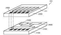
- FIG. 8 is a schematic view showing an example of the configuration of the image pickup apparatus 101 according to the present embodiment.
- the image pickup apparatus 101 includes a first substrate 2000 and a second substrate 2100 laminated on the first substrate 2000.
- the first substrate 2000 is located above the second substrate.
- the first substrate 2000 has a pixel array 111.
- the pixel array 111 has, for example, a structure in which the above-mentioned pixels 110, pixels 110A, or pixels 115 are arranged in a matrix.
- the second substrate 2100 receives an analog-to-digital conversion circuit (AD conversion circuit) 2200 that receives a signal output (specifically, an analog signal) from each pixel included in the pixel array 111 and converts it into a digital signal, and an analog. It has a memory 2400 for storing a signal converted into a digital signal by the digital conversion circuit 2200, and an arithmetic processing circuit 2300 for arithmetically processing the signal converted into a digital signal by the analog-digital conversion circuit 2200.
- AD conversion circuit analog-to-digital conversion circuit
- the first substrate 2000 and the second substrate 2100 are electrically connected by a connecting portion 2500.
- the pixel 110, the pixel 110A, or the pixel 115 for realizing the above-mentioned image pickup apparatus 100 is provided on the first substrate 2000, and is a circuit for controlling the counter electrode 1b of the photoelectric conversion unit 1.
- the circuit for the interrupt control logic is provided on the second substrate 2100.
- the circuit for controlling the counter electrode 1b of the photoelectric conversion unit 1 and the circuit for interrupt control logic are provided on the second substrate 2100.
- the pixel 110, the pixel 110A, or the pixel 115 is provided on the first substrate 2000, and the vertical operation circuit 141, the voltage supply circuit 140, the column signal processing circuit 142, and the horizontal signal readout circuit 143 are the first. It is provided on the substrate 2100 of 2. Further, the switching circuit 20 may not be included in the pixel 110, the pixel 110A or the pixel 115, and the switching circuit 20 may be provided on the second substrate 2100. Further, the constant current source 144 may not be included in the first substrate 1000, and the constant current source 144 may be provided in the second substrate 2100.
- the laminated structure of the image pickup apparatus 101 is a structure in which two layers of substrates are laminated, but the present invention is not limited to this, and a structure in which three or more layers of substrates are laminated is not limited to this. Often, a structure in which a plurality of child substrates are laminated on a single-layer substrate may be used.
- the connection portion 2500 of the substrate may be provided for each row as shown in FIG. 8, may be provided for each region, or may be provided for each pixel.
- FIG. 9 is a block diagram showing an example of the configuration of the camera system 1000 according to the third embodiment.
- the camera system 1000 is for signal processing the image pickup device 102, the optical system 1001 for condensing light such as a lens, and the data taken by the image pickup device 102, and outputting the data as an image or data.
- the camera signal processing unit 1002 and the system controller 1003 for controlling the image pickup device 102 and the camera signal processing unit 1002 are provided.
- the optical system 1001 is a lens or the like for condensing light on the imaging surface of the imaging device 102.
- the light that has passed through the optical system 1001 is incident on the photoelectric conversion unit 1 of the image pickup apparatus 102, and is photoelectrically converted to generate a signal charge.
- the image pickup device 102 for example, the image pickup device 100 or 101 according to the above embodiment is used.
- the camera signal processing unit 1002 functions as a signal processing circuit that processes the output signal from the image pickup device 102.
- the camera signal processing unit 1002 performs processing such as gamma correction, color interpolation processing, spatial interpolation processing, auto white balance, distance measurement calculation, and wavelength information separation.
- the camera signal processing unit 1002 can be realized by, for example, a DSP (Digital Signal Processor) or the like.
- the system controller 1003 controls the entire camera system 1000.
- the system controller 1003 can be realized, for example, by a microcomputer.
- the camera system 1000 uses the image pickup device 100 or 101 according to the above embodiment as the image pickup device 102, so that the delay time from the reception of the trigger signal from the outside to the start of the exposure operation of the light receiving surface collectively is delayed. Can be shortened. Therefore, it is possible to provide a highly usable camera system 1000 that has a short waiting time until the start of the exposure operation, enables imaging when an image is desired to be captured, or enables high-speed inspection.
- the reset operation in step S14 is started immediately after the operation in step S13 is completed, but after the operation in step S13 is completed within the range in which the image quality required for the purpose of use can be obtained. It may be started at intervals from.
- the charge storage unit FD in the reset operation, is electrically connected to the switching circuit 20, so that the voltage of the charge storage unit FD becomes equal to the reset voltage VRST, but the present invention is limited to this. Absent.
- a reset operation may be performed by applying a reference voltage from a circuit different from the switching circuit 20 in the charge storage unit FD.
- the photoelectric conversion unit 1 includes the pixel electrode 1a, the counter electrode 1b, and the photoelectric conversion layer 1c, but further, between the photoelectric conversion layer 1c and the pixel electrode 1a or the counter electrode 1b. May include a charge transport layer or a charge blocking layer. As a result, the generation of dark current is further suppressed, so that noise is further reduced.
- the trigger signal is received during a period other than the pre-reset operation period. For example, if the trigger signal is received before the pre-reset operation is started, the trigger signal may be ignored. Alternatively, after receiving the trigger signal, the reset operation may be performed on all the pixels in the row, and then the exposure operation may be started. Further, for example, when the trigger signal is received during the exposure period, the trigger signal may be ignored. Alternatively, after the end of the exposure operation, the signal reading operation and the reset operation may be performed, and then the exposure operation may be performed again. Alternatively, the reset operation may be performed after the end of the exposure operation, and then the exposure operation may be performed again.
- the exposure operation may be interrupted in the middle, the reset operation may be performed, and then the exposure operation may be performed again. Even if the above-mentioned operation is performed when the trigger signal is received during a period other than the pre-reset operation period, it is included in the scope of rights of the present disclosure as long as the operation described in the claims of the present disclosure is performed.
- the imaging device can be used in various camera systems and sensor systems such as digital still cameras, medical cameras, surveillance cameras, in-vehicle cameras, digital single-lens reflex cameras, and digital mirrorless single-lens cameras. ..
Landscapes
- Engineering & Computer Science (AREA)
- Multimedia (AREA)
- Signal Processing (AREA)
- Solid State Image Pick-Up Elements (AREA)
- Transforming Light Signals Into Electric Signals (AREA)
Abstract
Description
前述の、CDS技術においては、光信号を検出するPD部で発生した信号電荷を、電圧信号へと変換するFD部へと転送する際に完全転送が前提となる。完全転送を実現するためにはプロセスが複雑化し、製造コストが増加するなどの課題がある。
はじめに、図1Aから図3を参照して、本実施の形態に係る撮像装置100の構造を説明する。
図1Aは、本実施の形態に係る撮像装置100の例示的な回路構成を模式的に示す図である。撮像装置100は、一例として積層型の撮像素子であり、半導体基板に積層された光電変換層を有している。撮像装置100は、複数の画素110と周辺回路とを備える。周辺回路は、複数の画素110の動作を制御する制御回路を含む。制御回路は、外部からのトリガ信号を受け取り、複数の画素110に露光動作を行わせる。
次に、撮像装置100の複数の画素110の動作について説明する。撮像装置100の制御回路は、複数の画素110に、信号電荷を電荷蓄積部FDに蓄積する露光動作、電荷蓄積部FDの電位を初期化するリセット動作、及び、電荷蓄積部FDに蓄積された信号電荷に対応する信号を出力する読み出し動作を行わせる。画素110の代わりに画素110A又は画素115が用いられる場合も、基本的な動作は同じである。
次に、撮像装置100の動作について説明する。具体的には、撮像装置100の制御回路が、複数の画素に行わせる動作について説明する。
次に、実施の形態2について説明する。実施の形態2では、少なくとも2層の基板の積層構造を有する撮像装置について説明する。
次に、実施の形態3について説明する。実施の形態3では、上記撮像装置を備えるカメラシステムについて説明する。図9は、実施の形態3に係るカメラシステム1000の構成の一例を示すブロック図である。
以上、1つ又は複数の態様に係る撮像装置及びカメラシステムについて、各実施の形態に基づいて説明したが、本開示は、これらの実施の形態に限定されるものではない。
1a 画素電極
1b 対向電極
1c 光電変換層
2 増幅器
3、3A 帯域制御部
5 出力選択部
9 第1の容量素子
10 第2の容量素子
11 第1のスイッチ素子
12 第2のスイッチ素子
13、13A 帯域制御回路
14A リセット回路
30、30A フィードバック回路
41 電荷蓄積ノード
42 増幅トランジスタ
42g、44g、46g ゲート絶縁層
42e、44e、46e ゲート電極
44 選択トランジスタ
46、46A 帯域制御トランジスタ
48 リセットトランジスタ
50、50A 読み出し回路
62 半導体基板
62a、62b、62c、62d、62e 不純物領域
62s 素子分離領域
63A、63B、63C、63D 層間絶縁層
65A、65B コンタクトプラグ
66A、68A、68B 配線
67A、67B、67C、67D、67E プラグ
72 カラーフィルタ
74 マイクロレンズ
100、101、102 撮像装置
110、110A、115 画素
111 画素アレイ
120 電源線
130 蓄積制御線
141 垂直走査回路
142 カラム信号処理回路
143 水平信号読み出し回路
144 定電流源
170 信号読み出し信号線
180 水平共通信号線
1000 カメラシステム
1001 光学系
1002 カメラ信号処理部
1003 システムコントローラ
2000 第1の基板
2100 第2の基板
2200 アナログ-デジタル変換回路
2300 演算処理回路
2400 メモリ
2500 接続部
CON2 リセット制御信号線
CON3 増幅制御信号線
CON7 選択制御信号線
Claims (12)
- 光を信号電荷に変換する光電変換部と、前記信号電荷を蓄積する電荷蓄積部とをそれぞれが含み、行列状に配列される複数の画素と、
制御回路と
を備え、
前記制御回路は、
露光開始を指示するトリガ信号を受け取るまでに、前記電荷蓄積部の電位を初期化するリセット動作を、前記複数の画素のうち少なくとも1つの行に属する画素に行単位または複数行単位で順に行わせ、
前記トリガ信号を受け取った後、前記複数の画素のうち少なくとも1つの行に属する画素に前記リセット動作を行わせることなく、前記信号電荷を前記電荷蓄積部に蓄積する露光動作を前記複数の画素に同時に行わせる、
撮像装置。 - 前記制御回路は、前記トリガ信号を受け取るまでに、前記リセット動作を前記複数の画素のすべての画素に行単位または複数行単位で順に行わせる、
請求項1に記載の撮像装置。 - 前記制御回路は、前記トリガ信号を受け取るまでに、前記複数の画素のうち少なくとも1つの行に属する画素に前記リセット動作を複数回行わせる、
請求項1又は2に記載の撮像装置。 - 前記制御回路は、前記トリガ信号を受け取るまで、前記複数の画素に、前記リセット動作を行単位または複数行単位で順に繰り返し行わせる、
請求項1から3のいずれか一項に記載の撮像装置。 - 前記制御回路は、前記露光動作の後、前記電荷蓄積部に蓄積された前記信号電荷に対応する信号を出力する読み出し動作を、前記リセット動作を開始した行から行単位または複数行単位で順に前記複数の画素に行わせる、
請求項1から4のいずれか一項に記載の撮像装置。 - 前記制御回路は、
前記リセット動作を、前記リセット動作を開始した行とは異なる行まで行単位または複数行単位で順に前記複数の画素に行わせ、
前記露光動作の後、前記電荷蓄積部に蓄積された前記信号電荷に対応する信号を出力する読み出し動作を、前記リセット動作を終了した行の次の順番の行から行単位または複数行単位で順に前記複数の画素に行わせる、
請求項1から4のいずれか一項に記載の撮像装置。 - 前記複数の画素のそれぞれは、前記リセット動作において前記電荷蓄積部の電位を負帰還させるフィードバック回路を含む、
請求項1から6のいずれか一項に記載の撮像装置。 - 前記複数の画素のそれぞれは、前記リセット動作において発生するリセットノイズを抑制する回路を含む、
請求項1から7のいずれか一項に記載の撮像装置。 - 前記リセット動作は、前記電荷蓄積部の電位を負帰還させる動作を含む、請求項1から8のいずれか一項に記載の撮像装置。
- 電圧供給回路をさらに備え、
前記光電変換部は、前記電圧供給回路に電気的に接続される対向電極と、前記電荷蓄積部に電気的に接続される画素電極と、前記対向電極と前記画素電極との間に位置する光電変換層とを含み、
前記制御回路は、前記電圧供給回路に前記対向電極へ電圧を印加させて、前記光電変換層内に電界を形成させることにより、前記複数の画素に前記露光動作を行わせる、
請求項1から9のいずれか一項に記載の撮像装置。 - 光を信号電荷に変換する光電変換部と、前記信号電荷を蓄積する電荷蓄積部とをそれぞれが含み、行列状に配列される複数の画素を備える撮像装置の制御方法であって、
露光開始を指示するトリガ信号を受け取るまでに、前記電荷蓄積部の電位を初期化するリセット動作を、前記複数の画素のうち少なくとも1つの行に属する画素に行単位または複数行単位で順に行い、
前記トリガ信号を受け取った後、前記複数の画素のうち少なくとも1つの行に属する画素に前記リセット動作を行うことなく、前記信号電荷を前記電荷蓄積部に蓄積する露光動作を前記複数の画素に同時に行う、
制御方法。 - 前記リセット動作は、前記電荷蓄積部の電位を負帰還させる動作を含む、請求項11に記載の撮像装置。
Priority Applications (4)
| Application Number | Priority Date | Filing Date | Title |
|---|---|---|---|
| CN202080076398.0A CN114631308B (zh) | 2019-11-29 | 2020-08-26 | 摄像装置及控制方法 |
| JP2021561164A JP7599135B2 (ja) | 2019-11-29 | 2020-08-26 | 撮像装置及び制御方法 |
| EP20894775.4A EP4068362B1 (en) | 2019-11-29 | 2020-08-26 | Image capturing device and control method |
| US17/660,829 US12348681B2 (en) | 2019-11-29 | 2022-04-26 | Imaging device and control method |
Applications Claiming Priority (2)
| Application Number | Priority Date | Filing Date | Title |
|---|---|---|---|
| JP2019-216966 | 2019-11-29 | ||
| JP2019216966 | 2019-11-29 |
Related Child Applications (1)
| Application Number | Title | Priority Date | Filing Date |
|---|---|---|---|
| US17/660,829 Continuation US12348681B2 (en) | 2019-11-29 | 2022-04-26 | Imaging device and control method |
Publications (1)
| Publication Number | Publication Date |
|---|---|
| WO2021106294A1 true WO2021106294A1 (ja) | 2021-06-03 |
Family
ID=76130450
Family Applications (1)
| Application Number | Title | Priority Date | Filing Date |
|---|---|---|---|
| PCT/JP2020/032206 Ceased WO2021106294A1 (ja) | 2019-11-29 | 2020-08-26 | 撮像装置及び制御方法 |
Country Status (5)
| Country | Link |
|---|---|
| US (1) | US12348681B2 (ja) |
| EP (1) | EP4068362B1 (ja) |
| JP (1) | JP7599135B2 (ja) |
| CN (1) | CN114631308B (ja) |
| WO (1) | WO2021106294A1 (ja) |
Families Citing this family (1)
| Publication number | Priority date | Publication date | Assignee | Title |
|---|---|---|---|---|
| CN120916073B (zh) * | 2025-10-10 | 2026-02-03 | 创视半导体(杭州)有限公司 | 一种提高图像传感器帧率的方法 |
Citations (8)
| Publication number | Priority date | Publication date | Assignee | Title |
|---|---|---|---|---|
| JP2001177084A (ja) | 1999-12-14 | 2001-06-29 | Olympus Optical Co Ltd | 固体撮像素子 |
| JP2008028516A (ja) | 2006-07-19 | 2008-02-07 | Olympus Corp | カメラシステム |
| JP2010129705A (ja) | 2008-11-27 | 2010-06-10 | Nikon Corp | 固体撮像素子及びその製造方法 |
| JP2010258682A (ja) | 2009-04-23 | 2010-11-11 | Olympus Corp | 固体撮像装置及びカメラシステム |
| JP2012129817A (ja) * | 2010-12-15 | 2012-07-05 | Canon Inc | 撮像装置及び撮像素子の制御方法 |
| JP2014078870A (ja) | 2012-10-11 | 2014-05-01 | Fujifilm Corp | 固体撮像素子および撮像装置 |
| WO2018055948A1 (ja) * | 2016-09-23 | 2018-03-29 | 富士フイルム株式会社 | 撮像装置、撮像装置の作動方法、撮像装置の作動プログラム |
| US10225500B2 (en) | 2016-01-22 | 2019-03-05 | Panasonic Intellectual Property Management Co., Ltd. | Imaging device including output signal lines for each column |
Family Cites Families (7)
| Publication number | Priority date | Publication date | Assignee | Title |
|---|---|---|---|---|
| JP4025836B2 (ja) * | 2004-10-07 | 2007-12-26 | コニカミノルタオプト株式会社 | 撮像装置及び携帯通信機器 |
| JP2010166159A (ja) | 2009-01-13 | 2010-07-29 | Olympus Imaging Corp | カメラ、カメラのぶれ補正方法 |
| JP6175651B2 (ja) * | 2012-12-05 | 2017-08-09 | パナソニックIpマネジメント株式会社 | 固体撮像装置 |
| US9737271B2 (en) * | 2014-04-09 | 2017-08-22 | Canon Kabushiki Kaisha | Radiation imaging apparatus and control method of the same |
| CN111901540B (zh) * | 2014-12-26 | 2023-05-23 | 松下知识产权经营株式会社 | 摄像装置 |
| CN112929586B (zh) * | 2015-12-03 | 2024-12-06 | 松下知识产权经营株式会社 | 摄像装置 |
| WO2018173597A1 (ja) | 2017-03-22 | 2018-09-27 | 富士フイルム株式会社 | 撮像装置、撮像方法、及び撮像プログラム |
-
2020
- 2020-08-26 EP EP20894775.4A patent/EP4068362B1/en active Active
- 2020-08-26 WO PCT/JP2020/032206 patent/WO2021106294A1/ja not_active Ceased
- 2020-08-26 CN CN202080076398.0A patent/CN114631308B/zh active Active
- 2020-08-26 JP JP2021561164A patent/JP7599135B2/ja active Active
-
2022
- 2022-04-26 US US17/660,829 patent/US12348681B2/en active Active
Patent Citations (8)
| Publication number | Priority date | Publication date | Assignee | Title |
|---|---|---|---|---|
| JP2001177084A (ja) | 1999-12-14 | 2001-06-29 | Olympus Optical Co Ltd | 固体撮像素子 |
| JP2008028516A (ja) | 2006-07-19 | 2008-02-07 | Olympus Corp | カメラシステム |
| JP2010129705A (ja) | 2008-11-27 | 2010-06-10 | Nikon Corp | 固体撮像素子及びその製造方法 |
| JP2010258682A (ja) | 2009-04-23 | 2010-11-11 | Olympus Corp | 固体撮像装置及びカメラシステム |
| JP2012129817A (ja) * | 2010-12-15 | 2012-07-05 | Canon Inc | 撮像装置及び撮像素子の制御方法 |
| JP2014078870A (ja) | 2012-10-11 | 2014-05-01 | Fujifilm Corp | 固体撮像素子および撮像装置 |
| US10225500B2 (en) | 2016-01-22 | 2019-03-05 | Panasonic Intellectual Property Management Co., Ltd. | Imaging device including output signal lines for each column |
| WO2018055948A1 (ja) * | 2016-09-23 | 2018-03-29 | 富士フイルム株式会社 | 撮像装置、撮像装置の作動方法、撮像装置の作動プログラム |
Non-Patent Citations (1)
| Title |
|---|
| See also references of EP4068362A4 |
Also Published As
| Publication number | Publication date |
|---|---|
| CN114631308B (zh) | 2026-03-31 |
| CN114631308A (zh) | 2022-06-14 |
| JPWO2021106294A1 (ja) | 2021-06-03 |
| EP4068362A4 (en) | 2023-01-11 |
| JP7599135B2 (ja) | 2024-12-13 |
| US12348681B2 (en) | 2025-07-01 |
| EP4068362A1 (en) | 2022-10-05 |
| EP4068362B1 (en) | 2025-07-09 |
| US20220256106A1 (en) | 2022-08-11 |
Similar Documents
| Publication | Publication Date | Title |
|---|---|---|
| US11050966B2 (en) | Solid-state imaging device, method for driving solid-state imaging device, and electronic apparatus | |
| US9961262B2 (en) | Solid-state imaging device having a switchable conversion gain in the floating diffusion, method for driving solid-state imaging device, and electronic apparatus | |
| CN111901540B (zh) | 摄像装置 | |
| US10559614B2 (en) | Dual conversion gain circuitry with buried channels | |
| US20130113966A1 (en) | Solid-state imaging apparatus | |
| KR101989907B1 (ko) | 유기 이미지 센서 및 그 제조방법 | |
| US10854649B2 (en) | Image sensor including unit pixel block having common selection transistor | |
| KR20160137953A (ko) | 고체 촬상 소자 및 촬상 장치 | |
| JP6351423B2 (ja) | 撮像装置及び撮像システム | |
| US20220102401A1 (en) | Image sensing device | |
| JP2016015680A (ja) | 固体撮像素子および撮像装置 | |
| TWI833639B (zh) | 固體攝像裝置、固體攝像裝置的驅動方法以及電子設備 | |
| US20160372511A1 (en) | Solid-state imaging device, imaging apparatus, and method of driving the solid-state imaging device | |
| CN114143483B (zh) | 图像感测装置 | |
| JP7599135B2 (ja) | 撮像装置及び制御方法 | |
| JP2025166024A (ja) | 撮像素子 | |
| JP7782144B2 (ja) | 撮像素子、及び、撮像装置 | |
| JP6863355B2 (ja) | 撮像素子および撮像装置 | |
| WO2023166832A1 (ja) | 撮像装置 |
Legal Events
| Date | Code | Title | Description |
|---|---|---|---|
| 121 | Ep: the epo has been informed by wipo that ep was designated in this application |
Ref document number: 20894775 Country of ref document: EP Kind code of ref document: A1 |
|
| ENP | Entry into the national phase |
Ref document number: 2021561164 Country of ref document: JP Kind code of ref document: A |
|
| NENP | Non-entry into the national phase |
Ref country code: DE |
|
| ENP | Entry into the national phase |
Ref document number: 2020894775 Country of ref document: EP Effective date: 20220629 |
|
| WWG | Wipo information: grant in national office |
Ref document number: 2020894775 Country of ref document: EP |