WO2021109426A1 - 体声波谐振器及制造方法、体声波谐振器单元、滤波器及电子设备 - Google Patents
体声波谐振器及制造方法、体声波谐振器单元、滤波器及电子设备 Download PDFInfo
- Publication number
- WO2021109426A1 WO2021109426A1 PCT/CN2020/086564 CN2020086564W WO2021109426A1 WO 2021109426 A1 WO2021109426 A1 WO 2021109426A1 CN 2020086564 W CN2020086564 W CN 2020086564W WO 2021109426 A1 WO2021109426 A1 WO 2021109426A1
- Authority
- WO
- WIPO (PCT)
- Prior art keywords
- single crystal
- bottom electrode
- piezoelectric layer
- thin film
- layer
- Prior art date
- Legal status (The legal status is an assumption and is not a legal conclusion. Google has not performed a legal analysis and makes no representation as to the accuracy of the status listed.)
- Ceased
Links
Images




Classifications
-
- H—ELECTRICITY
- H03—ELECTRONIC CIRCUITRY
- H03H—IMPEDANCE NETWORKS, e.g. RESONANT CIRCUITS; RESONATORS
- H03H9/00—Networks comprising electromechanical or electro-acoustic elements; Electromechanical resonators
- H03H9/15—Constructional features of resonators consisting of piezoelectric or electrostrictive material
- H03H9/17—Constructional features of resonators consisting of piezoelectric or electrostrictive material having a single resonator
- H03H9/171—Constructional features of resonators consisting of piezoelectric or electrostrictive material having a single resonator implemented with thin-film techniques, i.e. of the film bulk acoustic resonator [FBAR] type
-
- H—ELECTRICITY
- H03—ELECTRONIC CIRCUITRY
- H03H—IMPEDANCE NETWORKS, e.g. RESONANT CIRCUITS; RESONATORS
- H03H9/00—Networks comprising electromechanical or electro-acoustic elements; Electromechanical resonators
- H03H9/02—Details
- H03H9/02007—Details of bulk acoustic wave devices
- H03H9/02086—Means for compensation or elimination of undesirable effects
- H03H9/02118—Means for compensation or elimination of undesirable effects of lateral leakage between adjacent resonators
-
- H—ELECTRICITY
- H03—ELECTRONIC CIRCUITRY
- H03H—IMPEDANCE NETWORKS, e.g. RESONANT CIRCUITS; RESONATORS
- H03H3/00—Apparatus or processes specially adapted for the manufacture of impedance networks, resonating circuits, resonators
- H03H3/007—Apparatus or processes specially adapted for the manufacture of impedance networks, resonating circuits, resonators for the manufacture of electromechanical resonators or networks
- H03H3/02—Apparatus or processes specially adapted for the manufacture of impedance networks, resonating circuits, resonators for the manufacture of electromechanical resonators or networks for the manufacture of piezoelectric or electrostrictive resonators or networks
-
- H—ELECTRICITY
- H03—ELECTRONIC CIRCUITRY
- H03H—IMPEDANCE NETWORKS, e.g. RESONANT CIRCUITS; RESONATORS
- H03H9/00—Networks comprising electromechanical or electro-acoustic elements; Electromechanical resonators
- H03H9/02—Details
- H03H9/02007—Details of bulk acoustic wave devices
-
- H—ELECTRICITY
- H03—ELECTRONIC CIRCUITRY
- H03H—IMPEDANCE NETWORKS, e.g. RESONANT CIRCUITS; RESONATORS
- H03H9/00—Networks comprising electromechanical or electro-acoustic elements; Electromechanical resonators
- H03H9/02—Details
- H03H9/05—Holders or supports
- H03H9/0504—Holders or supports for bulk acoustic wave devices
- H03H9/0514—Holders or supports for bulk acoustic wave devices consisting of mounting pads or bumps
- H03H9/0523—Holders or supports for bulk acoustic wave devices consisting of mounting pads or bumps for flip-chip mounting
-
- H—ELECTRICITY
- H03—ELECTRONIC CIRCUITRY
- H03H—IMPEDANCE NETWORKS, e.g. RESONANT CIRCUITS; RESONATORS
- H03H9/00—Networks comprising electromechanical or electro-acoustic elements; Electromechanical resonators
- H03H9/02—Details
- H03H9/05—Holders or supports
- H03H9/10—Mounting in enclosures
- H03H9/1007—Mounting in enclosures for bulk acoustic wave [BAW] devices
- H03H9/105—Mounting in enclosures for bulk acoustic wave [BAW] devices the enclosure being defined by a cover cap mounted on an element forming part of the BAW device
-
- H—ELECTRICITY
- H03—ELECTRONIC CIRCUITRY
- H03H—IMPEDANCE NETWORKS, e.g. RESONANT CIRCUITS; RESONATORS
- H03H9/00—Networks comprising electromechanical or electro-acoustic elements; Electromechanical resonators
- H03H9/15—Constructional features of resonators consisting of piezoelectric or electrostrictive material
- H03H9/17—Constructional features of resonators consisting of piezoelectric or electrostrictive material having a single resonator
- H03H9/171—Constructional features of resonators consisting of piezoelectric or electrostrictive material having a single resonator implemented with thin-film techniques, i.e. of the film bulk acoustic resonator [FBAR] type
- H03H9/172—Means for mounting on a substrate, i.e. means constituting the material interface confining the waves to a volume
- H03H9/173—Air-gaps
-
- H—ELECTRICITY
- H03—ELECTRONIC CIRCUITRY
- H03H—IMPEDANCE NETWORKS, e.g. RESONANT CIRCUITS; RESONATORS
- H03H9/00—Networks comprising electromechanical or electro-acoustic elements; Electromechanical resonators
- H03H9/15—Constructional features of resonators consisting of piezoelectric or electrostrictive material
- H03H9/17—Constructional features of resonators consisting of piezoelectric or electrostrictive material having a single resonator
- H03H9/171—Constructional features of resonators consisting of piezoelectric or electrostrictive material having a single resonator implemented with thin-film techniques, i.e. of the film bulk acoustic resonator [FBAR] type
- H03H9/172—Means for mounting on a substrate, i.e. means constituting the material interface confining the waves to a volume
- H03H9/174—Membranes
-
- H—ELECTRICITY
- H03—ELECTRONIC CIRCUITRY
- H03H—IMPEDANCE NETWORKS, e.g. RESONANT CIRCUITS; RESONATORS
- H03H9/00—Networks comprising electromechanical or electro-acoustic elements; Electromechanical resonators
- H03H9/46—Filters
- H03H9/54—Filters comprising resonators of piezoelectric or electrostrictive material
-
- H—ELECTRICITY
- H03—ELECTRONIC CIRCUITRY
- H03H—IMPEDANCE NETWORKS, e.g. RESONANT CIRCUITS; RESONATORS
- H03H3/00—Apparatus or processes specially adapted for the manufacture of impedance networks, resonating circuits, resonators
- H03H3/007—Apparatus or processes specially adapted for the manufacture of impedance networks, resonating circuits, resonators for the manufacture of electromechanical resonators or networks
- H03H3/02—Apparatus or processes specially adapted for the manufacture of impedance networks, resonating circuits, resonators for the manufacture of electromechanical resonators or networks for the manufacture of piezoelectric or electrostrictive resonators or networks
- H03H2003/021—Apparatus or processes specially adapted for the manufacture of impedance networks, resonating circuits, resonators for the manufacture of electromechanical resonators or networks for the manufacture of piezoelectric or electrostrictive resonators or networks the resonators or networks being of the air-gap type
-
- H—ELECTRICITY
- H03—ELECTRONIC CIRCUITRY
- H03H—IMPEDANCE NETWORKS, e.g. RESONANT CIRCUITS; RESONATORS
- H03H3/00—Apparatus or processes specially adapted for the manufacture of impedance networks, resonating circuits, resonators
- H03H3/007—Apparatus or processes specially adapted for the manufacture of impedance networks, resonating circuits, resonators for the manufacture of electromechanical resonators or networks
- H03H3/02—Apparatus or processes specially adapted for the manufacture of impedance networks, resonating circuits, resonators for the manufacture of electromechanical resonators or networks for the manufacture of piezoelectric or electrostrictive resonators or networks
- H03H2003/023—Apparatus or processes specially adapted for the manufacture of impedance networks, resonating circuits, resonators for the manufacture of electromechanical resonators or networks for the manufacture of piezoelectric or electrostrictive resonators or networks the resonators or networks being of the membrane type
-
- H—ELECTRICITY
- H03—ELECTRONIC CIRCUITRY
- H03H—IMPEDANCE NETWORKS, e.g. RESONANT CIRCUITS; RESONATORS
- H03H9/00—Networks comprising electromechanical or electro-acoustic elements; Electromechanical resonators
- H03H9/02—Details
- H03H9/05—Holders or supports
- H03H9/0538—Constructional combinations of supports or holders with electromechanical or other electronic elements
- H03H9/0547—Constructional combinations of supports or holders with electromechanical or other electronic elements consisting of a vertical arrangement
- H03H9/0561—Constructional combinations of supports or holders with electromechanical or other electronic elements consisting of a vertical arrangement consisting of a multilayered structure
Definitions
- the embodiments of the present invention relate to the semiconductor field, and in particular to a bulk acoustic wave resonator, a filter having the resonator, a bulk acoustic wave resonator unit, and an electronic device having the resonator or the filter .
- FBAR thin film bulk acoustic resonator
- the main structure of the film bulk acoustic wave resonator is a "sandwich" structure composed of electrode-piezoelectric film-electrode, that is, a layer of piezoelectric material is sandwiched between two metal electrode layers.
- FBAR uses the inverse piezoelectric effect to convert the input electrical signal into mechanical resonance, and then uses the piezoelectric effect to convert the mechanical resonance into electrical signal output.
- the film bulk acoustic resonator mainly uses the longitudinal piezoelectric coefficient (d33) of the piezoelectric film to produce the piezoelectric effect, so its main operating mode is the longitudinal wave mode in the thickness direction.
- the traditional structure is shown in Figure 1A, where 01 is the substrate, 02 is the cavity, 03 is the bottom electrode and the bottom electrode spans both sides of the cavity, 04 is the piezoelectric layer, and 05 is the top electrode.
- the piezoelectric film materials used in traditional thin film bulk acoustic wave resonators are mostly polycrystalline nitride films prepared by physical or chemical deposition techniques such as magnetron sputtering, which have poor piezoelectric properties (mainly reflected in the low electromechanical coupling coefficient of the resonator ), high defect density (mainly reflected in the low quality factor of the resonator), poor heat dissipation (mainly reflected in the low power capacity of the resonator), and there are etched oblique end faces at both ends of the bottom electrode of the resonator as shown in the figure As shown by 06 in 1, because its surface is generally rough, the defects in the piezoelectric layer deposited on the oblique end faces of both ends of the bottom electrode as shown in the area d in Fig. 1 will be further enlarged. The existence of these defects will cause acoustic loss, thereby reducing the Q factor of the resonator, and it will not be able to meet the technical indicators such as lower
- a bulk acoustic wave resonator including:
- the bottom electrode is connected to the bottom electrode pin
- the top electrode which is connected to the top electrode pin
- the piezoelectric layer is arranged between the bottom electrode and the top electrode
- the piezoelectric layer is a single crystal thin film piezoelectric layer
- the overlapping area of the acoustic mirror, the bottom electrode, the top electrode and the piezoelectric layer in the thickness direction of the resonator constitutes an effective area of the resonator.
- both are spaced apart from the edge of the acoustic mirror.
- the acoustic mirror is an acoustic mirror cavity provided on the upper side of the substrate and is a blind cavity.
- the embodiment of the present invention also relates to a bulk acoustic wave resonator unit, including: the above-mentioned bulk acoustic wave resonator; and a packaging substrate on which a circuit is provided that is electrically connected to the top electrode and the bottom electrode of the resonator. Device.
- the present invention also relates to a method for manufacturing a single crystal film bulk acoustic wave resonator.
- the single crystal film bulk acoustic wave resonator includes a substrate; an acoustic mirror; a bottom electrode connected to the pins of the bottom electrode; and a top electrode leading to the top electrode.
- the feet are connected; and the single crystal thin film piezoelectric layer is arranged between the bottom electrode and the top electrode, and the method includes the steps:
- the non-pin end of the top electrode is spaced apart from the edge of the acoustic mirror in the projection in the thickness direction of the resonator;
- the non-lead end of the bottom electrode is spaced from the edge of the acoustic mirror in the projection of the thickness direction of the resonator.
- the embodiment of the present invention also relates to a filter including the above-mentioned single crystal thin film bulk acoustic wave resonator or unit and the single crystal thin film bulk acoustic wave resonator manufactured according to the above method.
- the embodiment of the present invention also relates to an electronic device, including the above-mentioned filter or the above-mentioned resonator or unit.
- Figure 1A is a schematic cross-sectional view of a conventional bulk acoustic wave resonator
- FIG. 1B is a schematic top view of a single crystal thin film bulk acoustic resonator according to an exemplary embodiment of the present invention
- Fig. 1C is a schematic partial cross-sectional view taken along A-A in Fig. 1B according to an exemplary embodiment of the present invention
- FIG. 2 is a schematic cross-sectional view of a single crystal thin film bulk acoustic resonator according to another exemplary embodiment of the present invention.
- FIG. 3 is a schematic cross-sectional view of a single crystal thin film bulk acoustic wave resonator unit according to an exemplary embodiment of the present invention
- FIG. 4 is a schematic cross-sectional view of a single crystal thin film bulk acoustic wave resonator unit according to another exemplary embodiment of the present invention.
- 5A-5D are process schematic diagrams of a method for manufacturing a single crystal thin film bulk acoustic resonator according to an exemplary embodiment of the present invention.
- 6A-6E are process schematic diagrams of a method for manufacturing a single crystal thin film bulk acoustic resonator according to an exemplary embodiment of the present invention.
- Fig. 1B is a top view of a single crystal piezoelectric film bulk acoustic resonator according to an exemplary embodiment of the present invention.
- 16 is the air gap or cavity of the single crystal thin film resonator
- 13 is the bottom electrode of the single crystal thin film resonator located above the air gap
- 12 is the single crystal thin film piezoelectric layer of the resonator
- 17 is the single crystal thin film resonator
- the top electrode of is located on the single crystal piezoelectric layer
- 19a is the electrode connection structure on the top electrode
- 19b is the electrode connection structure on the bottom electrode.
- the bottom electrode of the single crystal thin film resonator is located in the vertical direction within the cavity (the bottom electrode in the conventional structure is located above the cavity in the vertical direction) .
- Figure 1C is a partial schematic cross-sectional view taken along AA in Figure 1B, in which: 15 is the substrate, 16 is the air gap or cavity, 13 is the bottom electrode, 12 is the single crystal thin film piezoelectric layer, and in the single crystal
- the surface of the thin film piezoelectric layer may or may not have a seed layer
- 14 is the electrode connection structure of the bottom electrode
- 17 is the top electrode
- 18 is the bottom electrode pin layer on the upper surface of the single crystal piezoelectric layer.
- the area where the bottom electrode overlaps the single crystal thin film piezoelectric layer and the top electrode in the thickness direction of the resonator is the effective area of the single crystal thin film resonator, that is, the area shown in D in FIG. 1C.
- the cavity structure in the prior art is generally a through hole penetrating the substrate, but the shortcomings of the deep hole etched through hole are that the cavity shape and size control accuracy are poor, the process is complicated, and the electrode connection form is complicated.
- the excess packaging process covers the through holes.
- the acoustic mirror cavity 16 is a blind hole. In other words, the bottom of the acoustic mirror cavity is sealed, which simplifies the process flow, reduces the cost, improves the shape and size control accuracy, and the electrode connection is more reliable. , No additional through-hole packaging process is required.
- the parts of the top electrode and the bottom electrode in the effective area are both located in the cavity in the vertical direction, in other words, the non-lead end of the top electrode and the non-lead end of the bottom electrode are in the single
- the projections in the thickness direction of the crystalline thin film resonator are all spaced apart from the edge of the acoustic mirror. This can avoid the influence of sub-resonance and clutter in the edge part outside the effective area of the single crystal thin film resonator due to the overlap of the top electrode and the bottom electrode in the vertical direction, thereby effectively improving the Q value of the single crystal thin film resonator .
- the material of the piezoelectric layer is a single crystal piezoelectric film material, it can make up for the defects in the traditional piezoelectric film material, and can greatly improve the electromechanical coupling coefficient Kt 2 of the resonator, the quality factor Q value, and the power capacity.
- the insertion loss and the suppression rate of adjacent frequency bands of filters composed of single crystal thin film resonators made of single crystal piezoelectric materials have also been greatly improved.
- FIG. 2 is a cross-sectional view of a single crystal thin film bulk acoustic resonator according to another embodiment of the present invention.
- the structure of the single crystal thin film resonator shown in FIG. 2 is similar to the structure of the embodiment shown in FIG. 1C, except that there are frame structures at the edges of the top electrode 17 and the bottom electrode 13, that is, a raised structure 20 and a recessed structure 21.
- the acoustic wave will be at the boundary.
- the transmission is not continuous, so at the boundary, a part of the acoustic energy will be coupled and reflected into the effective excitation area, and converted into a piston acoustic wave mode perpendicular to the piezoelectric layer surface, so that the Q factor of the resonator is improved.
- the acoustic mirror is in the form of a cavity, but the present invention is not limited to this, and other forms, such as a Bragg reflective layer, may also be used.
- the cavity is located between the substrate and the sandwich structure of the single crystal thin film resonator, and the bottom electrode is located in the cavity. Cavity.
- FIG. 3 is a schematic cross-sectional view of a single crystal thin film bulk acoustic wave resonator unit according to an exemplary embodiment of the present invention, in which a packaging structure of the single crystal thin film bulk acoustic wave resonator is shown.
- the single crystal thin film resonator unit shown in FIG. 3 is different from the single crystal thin film resonator shown in FIG. 1C in that there is a packaging structure above the single crystal thin film resonator, and its components include: bonding layer 30, connection Pillars 31, solder balls 32, and package substrate 33.
- the packaging structure can isolate the single crystal thin film resonator from the external environment, and can prevent external environmental pollutants, such as external gas, steam, fluid and/or particulate pollution from entering the internal space or volume.
- the bottom electrode 13 is located in the cavity 15.
- FIG. 4 is a schematic cross-sectional view of a single crystal thin film bulk acoustic wave resonator unit according to another exemplary embodiment of the present invention, in which a packaging structure of the single crystal thin film bulk acoustic wave resonator is shown.
- the single crystal thin film resonator unit shown in FIG. 4 is similar to the single crystal thin film resonator unit shown in FIG.
- the existence of the insertion layer can increase the mechanical strength of the single crystal thin film resonator, improve its stability, and enable it to be better used in complex environments; at the same time, when the material of the insertion layer is the same as the substrate material, it can better make the substrate Bond with the insertion layer to improve its sealing performance.
- the bottom electrode 13 and the piezoelectric layer 12 are both located in the cavity 16.
- the bottom electrode and the single crystal piezoelectric layer are both located in the cavity in the vertical direction (the bottom electrode and the piezoelectric layer in the traditional structure are in the cavity They are located above the cavity in the vertical direction).
- the projection of the non-lead end of the top electrode and the non-lead end of the bottom electrode in the thickness direction of the single crystal thin film resonator is spaced from the edge of the acoustic mirror. This can further avoid the generation of clutter in the single crystal thin film resonator, better confine the acoustic wave in the effective area of the single crystal thin film resonator, and improve the Q value of the single crystal thin film resonator.
- the bottom electrode pin 14 passes through the single crystal piezoelectric layer 12 and is connected to the bottom electrode 13, and the bottom electrode pin 14 and the bottom electrode 13 are in contact with each other.
- the cavity of the acoustic mirror is connected in the same layer.
- the bottom electrode pin 14 passes through the single crystal piezoelectric layer 12 and is connected to the bottom electrode 13, but the bottom electrode pin 14 and the bottom electrode 13 are in the acoustic mirror space.
- the cavities are stacked and connected.
- the portion 18 of the bottom electrode pin 14 located on the upper side of the single crystal piezoelectric layer 12 and the top electrode 17 are arranged in the same layer.
- the resonator further includes a bottom electrode pin located on the upper side of the single crystal piezoelectric layer and the single crystal piezoelectric layer, and on the single crystal piezoelectric layer.
- the part of the bottom electrode pin located on the upper side of the single crystal piezoelectric layer is arranged in the same layer as the top electrode pin.
- the single crystal piezoelectric film bulk acoustic resonator not only has a higher electromechanical coupling coefficient and a higher Q value, but also has better performance than the film bulk acoustic resonator of traditional piezoelectric film materials.
- single-crystal piezoelectric films generally cannot be grown by simple physical or chemical deposition methods. Therefore, the structure and production method of resonators based on single-crystal piezoelectric films are completely different from those based on polycrystalline piezoelectric films, which means that they need to be resonant. Innovation in device structure and processing method.
- the invention enables the piezoelectric layer of the resonator to use single crystal piezoelectric materials, which can greatly improve the electromechanical coupling coefficient of the resonator and reduce the insertion loss of the filter.
- 5A-5D are process schematic diagrams of a method for manufacturing a single crystal thin film bulk acoustic resonator according to an exemplary embodiment of the present invention.
- the processing flow of the single crystal piezoelectric film bulk acoustic wave resonator will be exemplified below with reference to FIGS. 5A-5D.
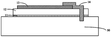
- a single crystal piezoelectric layer and bottom electrode are formed, as shown in FIG. 5A.
- the single crystal piezoelectric layer 12 is epitaxially grown on the substrate 50, which can be achieved by MOCVD (metal organic chemical vapor deposition), MBE (molecular beam epitaxy), chemical molecular beam epitaxy (CBE), liquid phase epitaxy (LPE), etc. Epitaxial growth method.
- MOCVD metal organic chemical vapor deposition
- MBE molecular beam epitaxy
- CBE chemical molecular beam epitaxy
- LPE liquid phase epitaxy
- a single crystal seed layer can be formed.
- a bottom electrode layer is deposited on the single crystal piezoelectric layer by CVD (chemical vapor deposition), PVD (physical vapor deposition), PECVD (plasma enhanced chemical vapor deposition), evaporation, sputtering and other similar thin film deposition processes 13.
- a bottom electrode connection layer is formed, as shown in FIG. 5B.
- through holes are etched in the single crystal piezoelectric layer 12 through the process of photolithography and etching, and the electrode connection layer 14 is formed to be connected to the bottom electrode 13 through the process of thin film deposition.
- the substrate 33 is combined with the single crystal piezoelectric layer 12 by a bonding method, and an auxiliary layer may exist between 33 and 12 to improve the bonding strength or to bond 33 and 12 together.
- an air gap 13 is formed between the substrate and the bottom electrode 13. The function of the air gap 13 is to confine sound waves within the resonator. Because the acoustic impedance of the air is close to zero, which does not match the acoustic impedance in the resonator, the acoustic wave can be reflected back into the effective area of the resonator and the Q factor of the resonator can be improved.
- the substrate 50 is removed, and the lead layer 18 of the top electrode 17 and the bottom electrode is formed.
- FIG. 5C Turn the structure in FIG. 5C over, with the substrate facing upwards, first reduce the thickness of the substrate 50 by mechanical grinding, and then completely remove the remaining substrate by etching. Then, a thin film is deposited to form the top electrode 17 and the bottom electrode pin layer 18 through photolithography and etching processes, and the pin layer is electrically connected to the bottom electrode connection layer 14.
- FIGS. 6A-6E are process schematic diagrams of a method for manufacturing a single crystal thin film bulk acoustic resonator according to another exemplary embodiment of the present invention.
- the processing flow of the single crystal piezoelectric film bulk acoustic wave resonator will be exemplified below with reference to FIGS. 6A-6E.
- a single crystal piezoelectric layer and a bottom electrode are formed.
- a single crystal seed layer 11 is epitaxially grown on the substrate 50, which can be achieved by MOCVD (Metal Organic Chemical Vapor Deposition), MBE (Molecular Beam Epitaxy) ), chemical molecular beam epitaxy (CBE), liquid phase epitaxy (LPE) and other similar epitaxial growth methods.
- MOCVD Metal Organic Chemical Vapor Deposition
- MBE Molecular Beam Epitaxy
- CBE chemical molecular beam epitaxy
- LPE liquid phase epitaxy
- the single crystal seed layer can also be used as a barrier layer for the etching process, which can prevent the piezoelectric layer from being etched in the subsequent processing.
- the single crystal seed layer can also promote the piezoelectric layer.
- the layer has a good crystal orientation during the epitaxial growth.
- the single crystal piezoelectric layer 12 is grown epitaxially.
- a bottom electrode layer is deposited on the single crystal piezoelectric layer by CVD (chemical vapor deposition), PVD (physical vapor deposition), PECVD (plasma enhanced chemical vapor deposition), evaporation, sputtering and other similar thin film deposition processes 13.
- a bottom electrode connection layer is formed, as shown in FIG. 6B.
- the excess part of the single crystal piezoelectric material and the seed layer is etched away by photolithography and etching processes, and both sides of the substrate 50 are exposed.
- a through hole for forming the bottom electrode connection layer 14 needs to be formed in the single crystal seed layer and the substrate. As shown in FIG. 6B, the through hole penetrates the single crystal seed layer 11 and extends into the substrate 50. Then, an electrode connection layer 14 is formed to be connected to the bottom electrode 13 through a thin film deposition process.
- the substrate 33 is combined with the substrate 33 by a bonding method.
- the direct bonding technology between the substrates such as Si-Si bonding, can be used between 33 and 50; there may also be an auxiliary layer to improve the bonding strength or use To glue 33 and 50 together.
- an air gap 13 is formed between the substrate 33 and the bottom electrode 13. The function of the air gap 13 is to confine sound waves within the resonator. Because the acoustic impedance of the air is close to zero, which does not match the acoustic impedance in the resonator, the acoustic wave can be reflected back into the effective area of the resonator and the Q factor of the resonator can be improved.
- the substrate 50 is then removed, and an insertion layer 40 is formed, as shown in the figure, with the through hole passing through the insertion layer.
- an insertion layer 40 is formed, as shown in the figure, with the through hole passing through the insertion layer.
- the existence of the insertion layer can increase the mechanical strength of the single crystal thin film resonator, improve its stability, and enable it to be better used in complex environments; at the same time, when the material of the insertion layer is the same as the substrate material, it can better make the substrate Bond with the insertion layer to improve its sealing performance.
- the bottom single crystal piezoelectric layer 12 can be prevented from being damaged during the process of removing the substrate by etching.
- the pin layer 18 of the top electrode 17 and the bottom electrode is formed.
- a layer of electrode film is formed by deposition, and the top electrode 17 and the pin layer 18 of the bottom electrode are formed by photolithography and etching processes.
- the pin layer 18 is connected to the electrode connecting layer 14 of the through hole or the bottom electrode. Make an electrical connection.
- the material of the single crystal piezoelectric layer may be: single crystal aluminum nitride, single crystal lithium niobate, single crystal lead zirconate titanate, single crystal potassium niobate, single crystal quartz film, or single crystal Lithium tantalate, etc.
- the material of the top electrode may be the following metals or their alloys: gold, tungsten, molybdenum, platinum, ruthenium, iridium, germanium, copper, titanium, titanium-tungsten, aluminum, chromium, and arsenic-doped gold.
- the material of the bottom electrode is the following metals or their alloys: gold, tungsten, molybdenum, platinum, ruthenium, iridium, germanium, copper, titanium, titanium tungsten, aluminum, chromium, and arsenic-doped gold.
- the materials of the top electrode and the bottom electrode are generally the same, but they can also be different.
- the base material includes: Si, quartz, single crystal AlN, LiNbO 3 , TaNbO 3 , SiC, GaN, GaAs, PZT, sapphire, diamond, etc.
- the mentioned numerical range can be not only the endpoint value, but also the median value between the endpoint values or other values, all of which fall within the protection scope of the present invention.
- the bulk acoustic wave resonator according to the present invention can be used to form a filter or other semiconductor devices.
- a bulk acoustic wave resonator including:
- the bottom electrode is connected to the bottom electrode pin
- the top electrode which is connected to the top electrode pin
- the piezoelectric layer is arranged between the bottom electrode and the top electrode
- the piezoelectric layer is a single crystal thin film piezoelectric layer
- the overlapping area of the acoustic mirror, the bottom electrode, the top electrode and the piezoelectric layer in the thickness direction of the resonator constitutes an effective area of the resonator.
- both are spaced apart from the edge of the acoustic mirror.
- the acoustic mirror is an acoustic mirror cavity arranged on the upper side of the substrate and is a blind hole.
- the bottom electrode is located in the cavity of the acoustic mirror or both the bottom electrode and the piezoelectric layer are located in the cavity of the acoustic mirror.
- the bottom electrode pin passes through the piezoelectric layer through hole of the piezoelectric layer to be connected to the bottom electrode, and the portion of the bottom electrode pin on the upper side of the piezoelectric layer is arranged on the same layer as the top electrode.
- the bottom electrode pin passes through the piezoelectric layer through hole of the piezoelectric layer to connect with the bottom electrode
- the resonator further includes an insertion layer between the bottom electrode pin on the upper side of the piezoelectric layer and the piezoelectric layer, and between the top electrode on the upper side of the piezoelectric layer and the piezoelectric layer;
- the part of the bottom electrode pin located on the upper side of the piezoelectric layer is arranged in the same layer as the top electrode pin.
- the bottom electrode pin and the bottom electrode are connected in the same layer in the acoustic mirror cavity; or the bottom electrode pin and the bottom electrode are stacked and connected in the acoustic mirror cavity.
- the piezoelectric layer through hole is located inside the edge of the acoustic mirror cavity.
- An acoustic impedance mismatch structure is provided on the lower side of the edge of the bottom electrode.
- the acoustic impedance mismatch structure includes a convex structure and a concave structure.
- the material of the single crystal piezoelectric layer is: single crystal aluminum nitride, single crystal lithium niobate, single crystal lead zirconate titanate, single crystal potassium niobate, single crystal quartz film or single crystal lithium tantalate.
- a bulk acoustic wave resonator unit comprising:
- the packaging substrate is provided with circuit devices which are respectively electrically connected to the top electrode and the bottom electrode of the resonator.
- the bottom electrode pin passes through the piezoelectric layer to be connected to the bottom electrode, and the portion of the bottom electrode pin located on the upper side of the piezoelectric layer is arranged in the same layer as the top electrode pin;
- the circuit device includes a bonding layer located on the lower side of the packaging substrate, and a conductive through hole passing through the packaging substrate, and the bonding layer and the conductive through hole are electrically connected to the corresponding electrode pins.
- a method for manufacturing a single crystal film bulk acoustic wave resonator the single crystal film bulk acoustic wave resonator comprising a substrate; an acoustic mirror; a bottom electrode connected to the bottom electrode pin; a top electrode connected to the top electrode pin
- the method includes the steps:
- the non-lead end of the top electrode is spaced apart from the edge of the acoustic mirror in the projection of the single crystal thin film resonator in the thickness direction;
- the non-lead end of the bottom electrode is spaced apart from the edge of the acoustic mirror in the projection in the thickness direction of the single crystal thin film resonator.
- a through hole is formed on the single crystal thin film piezoelectric layer, and an electrode connection layer of the bottom electrode is formed on one side of the single crystal thin film piezoelectric layer.
- the electrode connection layer of the bottom electrode is electrically connected to the bottom electrode and includes a through hole part;
- a substrate is arranged on the single crystal thin film piezoelectric layer, the substrate is provided with an acoustic mirror, and the substrate and the single crystal thin film piezoelectric layer are hermetically joined;
- a top electrode and a pin layer electrically connected to the through hole portion of the electrode connection layer of the bottom electrode are formed.
- a substrate is arranged on the single crystal thin film piezoelectric layer, the substrate is provided with an acoustic mirror, and the substrate and the single crystal thin film piezoelectric layer are hermetically joined;
- a top electrode and a pin layer electrically connected to the electrode connection layer of the bottom electrode are formed.
- the method further includes the step of forming a single crystal seed layer on the substrate;
- the through hole passes through the single crystal seed layer
- the top electrode is formed on the single crystal seed layer on the other side of the single crystal thin film piezoelectric layer.
- the method further includes the step of forming a single crystal seed layer on the substrate;
- the top electrode is formed on the single crystal seed layer on the other side of the single crystal thin film piezoelectric layer.
- the through hole penetrates the single crystal seed layer and extends into the substrate;
- the substrate is etched and an interposer structure is formed, the interposer structure extends to the inside of the edge of the acoustic mirror in the lateral direction ;
- the top electrode covers the interposer structure, and the lead layer of the bottom electrode covers The insertion layer structure, and the pin layer of the bottom electrode is electrically connected to the through hole.
- the acoustic mirror is an acoustic mirror cavity, and the cavity is formed between the substrate and the single crystal thin film piezoelectric layer, and the acoustic mirror cavity is a blind hole cavity.
- a filter comprising the bulk acoustic wave resonator according to any one of 1-11, or the bulk acoustic wave resonator unit according to 12 or 13, or any one of 14-20 Method for manufacturing single crystal thin film bulk acoustic wave resonator.
- An electronic device comprising the filter according to 21 or the bulk acoustic wave resonator according to any one of 1-11, or the bulk acoustic wave resonator unit according to 12 or 13, or according to 14- A single crystal thin film bulk acoustic resonator manufactured by the method of any one of 20.
Landscapes
- Physics & Mathematics (AREA)
- Acoustics & Sound (AREA)
- Engineering & Computer Science (AREA)
- Manufacturing & Machinery (AREA)
- Piezo-Electric Or Mechanical Vibrators, Or Delay Or Filter Circuits (AREA)
Abstract
本发明涉及一种单晶薄膜体声波谐振器,包括:基底;声学镜;底电极,与底电极引脚相接;顶电极,与顶电极引脚相接;和压电层,设置在底电极与顶电极之间,其中:所述压电层为单晶薄膜压电层;所述声学镜、底电极、顶电极和单晶薄膜压电层在谐振器的厚度方向上的重叠区域构成谐振器的有效区域。顶电极的非引脚端以及底电极的非引脚端在谐振器的厚度方向上的投影中,可均与声学镜的边缘间隔开。本发明还涉及一种单晶薄膜体声波谐振器的制造方法,一种具有上述单晶薄膜谐振器的单晶薄膜体声波谐振器单元以及一种电子设备。
Description
本发明的实施例涉及半导体领域,尤其涉及一种体声波谐振器、一种具有该谐振器的滤波器,一种体声波谐振器单元,以及一种具有该谐振器或者该滤波器的电子设备。
随着5G通信技术的日益发展,对通信频段的要求越来越高。传统的射频滤波器受结构和性能的限制,不能满足高频通信的要求。薄膜体声波谐振器(FBAR)作为一种新型的MEMS器件,很好地适应了无线通信系统的更新换代,使FBAR技术成为通信领域的研究热点之一。与传统的体声波谐振器相比,FBAR具有体积小、质量轻、插入损耗低、频带宽以及品质因子高等优点的薄膜体声波谐振器逐渐占领市场。
薄膜体声波谐振器的结构主体为由电极-压电薄膜-电极组成的“三明治”结构,即两层金属电极层之间夹一层压电材料。通过在两电极间输入正弦信号,FBAR利用逆压电效应将输入电信号转换为机械谐振,并且再利用压电效应将机械谐振转换为电信号输出。薄膜体声波谐振器主要利用压电薄膜的纵向压电系数(d33)产生压电效应,所以其主要工作模式为厚度方向上的纵波模式。其传统结构如图1A所示,其中01为基底,02为空腔,03为底电极且底电极跨越空腔的两侧,04为压电层,05为顶电极。
目前传统的薄膜体声波谐振器使用的压电薄膜材料大多采用磁控溅射等物理或化学沉积技术制备的多晶氮化物薄膜,压电特性较差(主要体现为谐振器机电耦合系数较低),缺陷密度较高(主要体现为谐振器品质因数较低),散热性不佳(主要体现为谐振器功率容量较低),而且在谐振器底电极两端存在的刻蚀斜端面如图1中的06所示,由于其表面一般比较粗糙,从而在底电极两端斜端面上沉积的压电层中如图1中的d区域所示缺陷会进一步放大。这些缺陷的存在会导致声学损失,从而使得谐振器 的Q因子减小,而且也无法满足未来移动通讯技术要求更低的插入损耗、更高的带宽等技术指标。
发明内容
为缓解或解决现有技术中的上述问题的至少一个方面,提出本发明。
根据本发明的实施例的一个方面,提出了一种体声波谐振器,包括:
基底;
声学镜;
底电极,与底电极引脚相接;
顶电极,与顶电极引脚相接;和
压电层,设置在底电极与顶电极之间,
其中:
所述压电层为单晶薄膜压电层;且
所述声学镜、底电极、顶电极和压电层在谐振器的厚度方向上的重叠区域构成谐振器的有效区域。
可选的,顶电极的非引脚端以及底电极的非引脚端在谐振器的厚度方向上的投影中,均与声学镜的边缘间隔开。
可选的,所述声学镜为设置于基底上侧的声学镜空腔且为盲孔空腔。
本发明的实施例还是涉及一种体声波谐振器单元,包括:上述的体声波谐振器;和封装基板,封装基板上设置有与所述谐振器的顶电极和底电极分别形成电连接的电路器件。
本发明还涉及一种单晶薄膜体声波谐振器的制造方法,所述单晶薄膜体声波谐振器包括基底;声学镜;底电极,与底电极引脚相接;顶电极,与顶电极引脚相接;和单晶薄膜压电层,设置在底电极与顶电极之间,所述方法包括步骤:
形成顶电极时,使得顶电极的非引脚端在谐振器的厚度方向上的投影中,与声学镜的边缘间隔开;和
形成底电极时,使得底电极的非引脚端在谐振器的厚度方向上的投影中,与声学镜的边缘间隔开。
本发明的实施例还涉及一种滤波器,包括上述的单晶薄膜体声波谐振 器或单元以及根据上述方法制造的单晶薄膜体声波谐振器。
本发明的实施例也涉及一种电子设备,包括上述的滤波器或者上述的谐振器或单元。
以下描述与附图可以更好地帮助理解本发明所公布的各种实施例中的这些和其他特点、优点,图中相同的附图标记始终表示相同的部件,其中:
图1A为传统体声波谐振器的截面示意图;
图1B为根据本发明的一个示例性实施例的单晶薄膜体声波谐振器的俯视示意图;
图1C为根据本发明的一个示例性实施例的沿图1B中的A-A截得的部分截面示意图;
图2为根据本发明的另一个示例性实施例的单晶薄膜体声波谐振器的截面示意图;
图3为根据本发明的一个示例性实施例的单晶薄膜体声波谐振器单元的截面示意图;
图4为根据本发明的另一个示例性实施例的单晶薄膜体声波谐振器单元的截面示意图;
图5A-5D为根据本发明的一个示例性实施例的单晶薄膜体声波谐振器的制造方法的过程示意图;
图6A-6E为根据本发明的一个示例性实施例的单晶薄膜体声波谐振器的制造方法的过程示意图。
下面通过实施例,并结合附图,对本发明的技术方案作进一步具体的说明。在说明书中,相同或相似的附图标号指示相同或相似的部件。下述参照附图对本发明实施方式的说明旨在对本发明的总体发明构思进行解 释,而不应当理解为对本发明的一种限制。发明的一部分实施例,而并不是全部的实施例。基于本发明中的实施例,本领域普通技术人员所获得的所有其他实施例,都属于本发明保护的范围。
图1B为根据本发明的一个示例性实施例的单晶压电薄膜体声波谐振器的俯视图。其中16为单晶薄膜谐振器的空气隙或空腔,13为单晶薄膜谐振器的底电极位于空气隙之上,12为谐振器的单晶薄膜压电层,17为单晶薄膜谐振器的顶电极位于单晶压电层之上,19a为位于顶电极上的电极连接结构,19b为位于底电极上的电极连接结构。与图1A中所示的传统结构不同的是,在图1B中,单晶薄膜谐振器的底电极在垂直方向上位于空腔之内(传统结构中底电极在垂直方向上位于空腔上方)。
图1C为沿图1B中的A-A所截的部分示意性截面图,其中:15为基底,16为空气隙或空腔,13为底电极,12为单晶薄膜压电层,另外在单晶薄膜压电层的表面可以有种子层也可以没有,14为底电极的电极连接结构,17为顶电极,18为位于单晶压电层上表面的底电极引脚层。其中底电极与单晶薄膜压电层和顶电极在谐振器厚度方向上重叠的区域为单晶薄膜谐振器的有效区域,即图1C中D所示区域。
另外,现有技术中的空腔结构,一般为穿透基底的通孔,,但深孔刻蚀通孔的缺点是空腔形状、尺寸控制精度差,且工艺复杂,电极连接形式复杂,需要多余的封装工艺覆盖通孔。而在本发明的一个实施例中,声学镜空腔16为盲孔,换言之,声学镜空腔下方是密封的,简化了工艺流程、降低了成本、提高了形状尺寸控制精度、电极连接更可靠、不需要额外的通孔封装流程。
在图1C所示实施例中,由于顶电极和底电极在有效区域的部分在垂直方向上都位于空腔之内,换言之,顶电极的非引脚端以及底电极的非引脚端在单晶薄膜谐振器的厚度方向上的投影中,均与声学镜的边缘间隔开。这能够避免在单晶薄膜谐振器有效区域外的边缘部分由于顶电极和底电极在垂直方向上重叠部分中产生的次谐振以及杂波的影响,进而能够有效提升单晶薄膜谐振器的Q值。
因为压电层的材料为单晶压电薄膜材料,能够弥补传统压电薄膜材 料中的缺陷问题,而且能够大幅提高谐振器的机电耦合系数Kt
2、品质因素Q值、功率容量等性能,而且采用单晶压电材料制作的单晶薄膜谐振器组成的滤波器的插入损耗、相邻频带的抑制率等性能也大幅提高。
图2为根据本发明的另外实施例的单晶薄膜体声波谐振器的截面图。在图2所示的单晶薄膜谐振器结构与图1C所示的实施例结构类似,不同之处在于在顶电极17和底电极13边缘处有框架结构即凸起结构20和凹陷结构21。在框架结构中具有第一声阻抗,在单晶薄膜谐振器的有效区域D中具有第二声阻抗,由于框架结构中的第一声阻抗和第二声阻抗不匹配,会使得声波在边界处传输不连续,因此在边界处,一部分声能就会耦合且反射到有效激励区域中,并且转换成与压电层表面垂直的活塞声波模式,从而使得谐振器的Q因子得到提高。
在图1C与图2所示的实施例中,声学镜为空腔的形式,但是本发明不限于此,也可以采用其他的形式,例如布拉格反射层。
在声学镜为空腔的情况下,如图1C和图2所示,在本发明的一个实施例中,该空腔位于基底与单晶薄膜谐振器的三明治结构之间,而且底电极位于空腔内。
图3为根据本发明的一个示例性实施例的单晶薄膜体声波谐振器单元的示意性截面图,其中示出了单晶薄膜体声波谐振器的封装结构。图3所示的单晶薄膜谐振器单元与图1C所示的单晶薄膜谐振器的不同之处在于在单晶薄膜谐振器的上方有封装结构,其组成部分包括:键合层30、连接柱31、焊球32和封装基板33。通过封装结构能够将单晶薄膜谐振器与外界环境隔离开来,能够防止外部环境污染物,例如外部气体、蒸汽、流体和/或微粒污染进入内部空间或体积。
如图3所示,在一个实施例中,底电极13位于空腔15内。
图4为根据本发明的另一个示例性实施例的单晶薄膜体声波谐振器单元的示意性截面图,其中示出了单晶薄膜体声波谐振器的封装结构。图4所示的单晶薄膜谐振器单元与图3所示的单晶薄膜谐振器单元相似,不同之处在于基底15之上有插入层40,其材料与基底15的材料相同或者不同。插入层的存在能够增加单晶薄膜谐振器的机械强度,提高其稳定性, 能够使其更好的应用在复杂的环境中;同时当插入层的材料与基底材料相同时,能够更好使基底与插入层进行键合,提高其密封性。
如图4所示,在一个实施例中,底电极13与压电层12均位于空腔16内。
如图3和4所示,根据本发明的单晶薄膜体声波谐振器单元中,底电极和单晶压电层在垂直方向上均位于空腔内(传统结构中底电极和压电层在垂直方向上均位于空腔上方),换言之,顶电极的非引脚端以及底电极的非引脚端在单晶薄膜谐振器的厚度方向上的投影中,均与声学镜的边缘间隔开。这能够进一步避免单晶薄膜谐振器中产生杂波,将声波更好的限定在单晶薄膜谐振器的有效区域中,提高单晶薄膜谐振器的Q值。
如图1C、2-3所示,在本发明的一个实施例中,底电极引脚14穿过单晶压电层12而与底电极13相接,底电极引脚14与底电极13在声学镜空腔内同层相接。
如图4所示,在本发明的一个实施例中,底电极引脚14穿过单晶压电层12而与底电极13相接,但是底电极引脚14与底电极13在声学镜空腔内层叠相接。
如图1C、2-3所示,在本发明的一个实施例中,底电极引脚14位于单晶压电层12上侧的部分18与顶电极17同层布置。
如图4所示,在本发明的一个实施例中,所述谐振器还包括位于单晶压电层上侧的底电极引脚与单晶压电层之间以及在单晶压电层上侧的顶电极与单晶压电层之间的插入层40。相应的,如图4所示,底电极引脚位于单晶压电层上侧的部分与顶电极引脚同层布置。
单晶压电薄膜体声波谐振器不仅具有较高的机电耦合系数、更高的Q值,且部分性能优于传统压电薄膜材料的薄膜体声波谐振器。但单晶压电薄膜一般无法通过简单的物理或化学沉积方式生长,所以基于单晶压电薄膜的谐振器结构以及制作方法完全不同于基于多晶压电薄膜的谐振器,意味着需要在谐振器结构和加工方法上的创新。本发明通过改变传统的FBAR结构及其加工制做方法,使得谐振器的压电层可以使用单晶压电材料,能够大幅提升谐振器的机电耦合系数、降低滤波器的插入损耗等。
图5A-5D为根据本发明的一个示例性实施例的单晶薄膜体声波谐振器的制造方法的过程示意图。下面参照图5A-5D示例性说明单晶压电薄膜体声波谐振器的加工工艺流程。
首先,形成单晶压电层和底电极,如图5A所示。先在衬底50上外延生长单晶压电层12,可以通过MOCVD(金属有机化学气相沉积)、MBE(分子束外延)、化学分子束外延(CBE)、液相外延(LPE)等类似的外延生长方法。可选的可以形成单晶种子层。然后在单晶压电层上通过CVD(化学气相沉积)、PVD(物理气相沉积)、PECVD(等离子体增强化学气相沉积)、蒸镀、溅射等类似的薄膜沉积工艺沉积一层底电极层13。
然后,形成底电极连接层,如图5B所示。通过光刻和刻蚀的工艺先在单晶压电层12中刻蚀出通孔,在通过薄膜沉积的工艺形成电极连接层14与底电极13相连。
之后,进行键合,如图5C所示。将基底33通过键合的方法与单晶压电层12结合,33与12之间可以有辅助层的存在,用于提高键合强度或用于将33与12粘接在一起。并在基底与底电极13之间形成空气隙13。空气隙13的作用是将声波限制谐振器内。因为空气的声阻抗接近为零,与谐振器中的声阻抗不匹配,因此能够将声波反射回谐振器有效区域内,提高谐振器的Q因子。
最后,如图5D所示,将衬底50去除,并形成顶电极17和底电极的引脚层18。将图5C中的结构翻转过来,使衬底朝上,先通过机械研磨的方法将衬底50减薄,然后在通过刻蚀的方法将剩余的衬底彻底去除。然后,沉积形成一层薄膜通过光刻、刻蚀工艺形成顶电极17,以及底电极的引脚层18,该引脚层与底电极连接层14电连接。
图6A-6E为根据本发明的另一个示例性实施例的单晶薄膜体声波谐振器的制造方法的过程示意图。下面参照图6A-6E示例性说明单晶压电薄膜体声波谐振器的加工工艺流程。
首先,形成单晶压电层和底电极,如图6A所示,首先在衬底50上外延生长一层单晶种子层11,可以通过MOCVD(金属有机化学气相沉积)、MBE(分子束外延)、化学分子束外延(CBE)、液相外延(LPE)等类似的 外延生长方法。单晶种子层的目的为促进单晶压电层在基底上的生长;种子层的材料可以与压电层11的材料不同。当种子层材料与压电层材料不同时,也可以作为刻蚀工艺阻挡层,在之后的加工过程中能够起到避免压电层被刻蚀的作用,同时单晶种子层也能促使压电层在外延生长的过程中具有良好的晶向。然后在外延生长单晶压电层12。然后在单晶压电层上通过CVD(化学气相沉积)、PVD(物理气相沉积)、PECVD(等离子体增强化学气相沉积)、蒸镀、溅射等类似的薄膜沉积工艺沉积一层底电极层13。
然后,形成底电极连接层,如图6B所示。通过光刻和刻蚀的工艺将单晶压电材料和种子层中多余的部分刻蚀掉,将衬底50的两侧露出。需要在单晶种子层以及衬底内形成供形成底电极连接层14的通孔,如图6B所示,通孔穿过单晶种子层11以及延伸到衬底50内。然后,通过薄膜沉积的工艺形成电极连接层14与底电极13相连。
之后,进行键合,如图6C所示。将基底33通过键合的方法与衬底33结合,33与50之间可采用基底间直接键合技术,如Si-Si键合;也可有辅助层存在,用于提高键合强度或用于将33与50粘接在一起。并在基底33与底电极13之间形成空气隙13。空气隙13的作用是将声波限制谐振器内。因为空气的声阻抗接近为零,与谐振器中的声阻抗不匹配,因此能够将声波反射回谐振器有效区域内,提高谐振器的Q因子。
此后,然后将衬底50去除,并形成插入层40,如图所示,通孔穿过该插入层。将图6C中的结构翻转过来,使衬底朝上,先通过机械研磨的方法将衬底50减薄,然后在通过刻蚀的方法将部分衬底彻底去除,形成插入层结构40。插入层的存在能够增加单晶薄膜谐振器的机械强度,提高其稳定性,能够使其更好的应用在复杂的环境中;同时当插入层的材料与基底材料相同时,能够更好使基底与插入层进行键合,提高其密封性。同时由于种子层11的存在,能够防止在刻蚀去除衬底的过程中对底部单晶压电层12的破坏。
最后,形成顶电极17与底电极的引脚层18。先沉积形成一层电极薄膜,在通过光刻、刻蚀工艺形成顶电极17以及底电极的引脚层18,如图6E所示,引脚层18与通孔或者底电极的电极连接层14形成电连接。
在本发明中,其中,单晶压电层的材料可以为:单晶氮化铝、单晶 铌酸锂、单晶锆钛酸铅、单晶铌酸钾、单晶石英薄膜、或者单晶钽酸锂等。
顶电极的材料可以为如下金属或者它们的合金:金、钨、钼、铂、钌、铱、锗、铜、钛、钛钨、铝、铬、砷掺杂金。同样地,底电极的材料为如下金属或者它们的合金:金、钨、钼、铂、钌、铱、锗、铜、钛、钛钨、铝、铬、砷掺杂金。顶电极和底电极材料一般相同,但也可以不同。
基底材料包括:Si、石英、单晶AlN、LiNbO
3、TaNbO
3、SiC、GaN、GaAs、PZT、蓝宝石、金刚石等。
在本发明中,提到的数值范围除了可以为端点值之外,还可以为端点值之间的中值或者其他值,均在本发明的保护范围之内。
如本领域技术人员能够理解的,根据本发明的体声波谐振器可以用于形成滤波器或其他半导体器件。
基于以上,本发明提出了如下技术方案:
1、一种体声波谐振器,包括:
基底;
声学镜;
底电极,与底电极引脚相接;
顶电极,与顶电极引脚相接;和
压电层,设置在底电极与顶电极之间,
其中:
所述压电层为单晶薄膜压电层;且
所述声学镜、底电极、顶电极和压电层在谐振器的厚度方向上的重叠区域构成谐振器的有效区域。
2、根据1所述的谐振器,其中:
顶电极的非引脚端以及底电极的非引脚端在谐振器的厚度方向上的投影中,均与声学镜的边缘间隔开。
3、根据1或2所述的谐振器,其中:
所述声学镜为设置于基底上侧的声学镜空腔且为盲孔。
4、根据3所述的谐振器,其中:
所述底电极位于所述声学镜空腔内或所述底电极与所述压电层均位于所述声学镜空腔内。
5、根据4所述的谐振器,其中:
所述底电极引脚穿过所述压电层的压电层通孔而与底电极相接,所述底电极引脚位于压电层上侧的部分与所述顶电极同层布置。
6、根据4所述的谐振器,其中:
所述底电极引脚穿过所述压电层的压电层通孔而与底电极相接;
所述谐振器还包括位于压电层上侧的底电极引脚与压电层之间以及在压电层上侧的顶电极与压电层之间的插入层;
所述底电极引脚位于压电层上侧的部分与所述顶电极引脚同层布置。
7、根据5或6所述的谐振器,其中:
所述底电极引脚与所述底电极在声学镜空腔内同层相接;或者所述底电极引脚与所述底电极在声学镜空腔内层叠相接。
8、根据5或6所述的谐振器,其中:
所述压电层通孔位于所述声学镜空腔的边缘的内侧。
9、根据1或2所述的谐振器,其中:
所述底电极的边缘的下侧设置有声阻抗不匹配结构。
10、根据9所述的谐振器,其中:
所述声阻抗不匹配结构包括凸起结构与凹陷结构。
11、根据1或2所述的谐振器,其中:
所述单晶压电层的材料为:单晶氮化铝、单晶铌酸锂、单晶锆钛酸铅、单晶铌酸钾、单晶石英薄膜或者单晶钽酸锂。
12、一种体声波谐振器单元,包括:
根据1-11中任一项所述的谐振器;和
封装基板,封装基板上设置有与所述谐振器的顶电极和底电极分别形成电连接的电路器件。
13、根据12所述的谐振器单元,其中:
所述底电极引脚穿过所述压电层而与底电极相接,所述底电极引脚位于压电层上侧的部分与所述顶电极引脚同层布置;且
所述电路器件包括位于封装基板的下侧的键合层,以及穿过封装基板的导电通孔,所述键合层与导电通孔与对应的电极引脚电连接。
14、一种单晶薄膜体声波谐振器的制造方法,所述单晶薄膜体声波谐 振器包括基底;声学镜;底电极,与底电极引脚相接;顶电极,与顶电极引脚相接;和单晶薄膜压电层,设置在底电极与顶电极之间,所述方法包括步骤:
形成顶电极时,使得顶电极的非引脚端在单晶薄膜谐振器的厚度方向上的投影中,与声学镜的边缘间隔开;和
形成底电极时,使得底电极的非引脚端在单晶薄膜谐振器的厚度方向上的投影中,与声学镜的边缘间隔开。
15、根据14所述的方法,包括步骤:
在衬底上依次形成单晶薄膜压电层与底电极;
在单晶薄膜压电层上形成通孔,以及在单晶薄膜压电层的一侧形成底电极的电极连接层,所述底电极的电极连接层与底电极电连接且包括位于通孔内的部分;
在单晶薄膜压电层上设置基底,所述基底设置有声学镜,且基底与单晶薄膜压电层密封接合;
移除在单晶薄膜压电层另一侧的衬底;
在单晶薄膜压电层的另一侧形成顶电极,以及与底电极的电极连接层的通孔部分电连接的引脚层。
16、根据14所述的方法,包括步骤:
在衬底上依次形成单晶薄膜压电层与底电极;
在单晶薄膜压电层的一侧形成底电极的电极连接层,所述底电极的电极连接层与底电极电连接;
在单晶薄膜压电层上设置基底,所述基底设置有声学镜,且基底与单晶薄膜压电层密封接合;
移除在单晶薄膜压电层另一侧的衬底;
在单晶薄膜压电层的另一侧形成顶电极,以及与底电极的电极连接层的电连接的引脚层。
17、根据15所述的方法,其中:
在“在衬底上依次形成单晶薄膜压电层与底电极”之前,还包括步骤:在衬底上形成单晶种子层;
步骤“在单晶薄膜压电层上形成通孔”中,通孔穿过所述单晶种子层;
在“在单晶薄膜压电层的另一侧形成顶电极”中,在单晶薄膜压电层的另一侧的单晶种子层上形成顶电极。
18、根据15所述的方法,其中:
在“在衬底上依次形成单晶薄膜压电层与底电极”之前,还包括步骤:在衬底上形成单晶种子层;
在“在单晶薄膜压电层的另一侧形成顶电极”中,在单晶薄膜压电层的另一侧的单晶种子层上形成顶电极。
19、根据15或16所述的方法,其中:
步骤“在单晶薄膜压电层上形成通孔”中,通孔穿过所述单晶种子层以及延伸到所述衬底内;
在“移除在单晶薄膜压电层另一侧的衬底”步骤中,刻蚀所述衬底且形成插入层结构,所述插入层结构在横向方向上延伸到声学镜的边缘的内侧;
“在单晶薄膜压电层的另一侧形成顶电极,以及与底电极的电极连接层的电连接的引脚层”中,顶电极覆盖所述插入层结构,底电极的引脚层覆盖所述插入层结构,且底电极的引脚层与所述通孔电连接。
20、根据14-19中任一项所述的方法,其中:
所述声学镜为声学镜空腔,且所述空腔形成在基底与单晶薄膜压电层之间,所述声学镜空腔为盲孔空腔。
21、一种滤波器,包括根据1-11中任一项所述的体声波谐振器,或者根据12或13所述的体声波谐振器单元,或者根据14-20中任一项所述的方法制造的单晶薄膜体声波谐振器。
22、一种电子设备,包括根据21所述的滤波器或者根据1-11中任一项所述的体声波谐振器,或者根据12或13所述的体声波谐振器单元,或根据14-20中任一项所述的方法制造的单晶薄膜体声波谐振器。
尽管已经示出和描述了本发明的实施例,对于本领域的普通技术人员而言,可以理解在不脱离本发明的原理和精神的情况下可以对这些实施例进行变化,本发明的范围由所附权利要求及其等同物限定。
Claims (22)
- 一种体声波谐振器,包括:基底;声学镜;底电极,与底电极引脚相接;顶电极,与顶电极引脚相接;和压电层,设置在底电极与顶电极之间,其中:所述压电层为单晶薄膜压电层;且所述声学镜、底电极、顶电极和压电层在谐振器的厚度方向上的重叠区域构成谐振器的有效区域。
- 根据权利要求1所述的谐振器,其中:顶电极的非引脚端以及底电极的非引脚端在谐振器的厚度方向上的投影中,均与声学镜的边缘间隔开。
- 根据权利要求1或2所述的谐振器,其中:所述声学镜为设置于基底上侧的声学镜空腔且为盲孔空腔。
- 根据权利要求3所述的谐振器,其中:所述底电极位于所述声学镜空腔内或所述底电极与所述压电层均位于所述声学镜空腔内。
- 根据权利要求4所述的谐振器,其中:所述底电极引脚穿过所述压电层的压电层通孔而与底电极相接,所述底电极引脚位于压电层上侧的部分与所述顶电极同层布置。
- 根据权利要求4所述的谐振器,其中:所述底电极引脚穿过所述压电层的压电层通孔而与底电极相接;所述谐振器还包括位于压电层上侧的底电极引脚与压电层之间以及在压电层上侧的顶电极与压电层之间的插入层;所述底电极引脚位于压电层上侧的部分与所述顶电极引脚同层布置。
- 根据权利要求5或6所述的谐振器,其中:所述底电极引脚与所述底电极在声学镜空腔内同层相接;或者所述底电极引脚与所述底电极在声学镜空腔内层叠相接。
- 根据权利要求5或6所述的谐振器,其中:所述压电层通孔位于所述声学镜空腔的边缘的内侧。
- 根据权利要求1或2所述的谐振器,其中:所述底电极的边缘的下侧设置有声阻抗不匹配结构。
- 根据权利要求9所述的谐振器,其中:所述声阻抗不匹配结构包括凸起结构与凹陷结构。
- 根据权利要求1或2所述的谐振器,其中:所述单晶压电层的材料为:单晶氮化铝、单晶铌酸锂、单晶锆钛酸铅、单晶铌酸钾、单晶石英薄膜或者单晶钽酸锂。
- 一种体声波谐振器单元,包括:根据权利要求1-11中任一项所述的谐振器;和封装基板,封装基板上设置有与所述谐振器的顶电极和底电极分别形成电连接的电路器件。
- 根据权利要求12所述的谐振器单元,其中:所述底电极引脚穿过所述压电层而与底电极相接,所述底电极引脚位于压电层上侧的部分与所述顶电极引脚同层布置;且所述电路器件包括位于封装基板的下侧的键合层,以及穿过封装基板的导电通孔,所述键合层与导电通孔与对应的电极引脚电连接。
- 一种单晶薄膜体声波谐振器的制造方法,所述单晶薄膜体声波谐振器包括基底;声学镜;底电极,与底电极引脚相接;顶电极,与顶电极引脚相接;和单晶薄膜压电层,设置在底电极与顶电极之间,所述方法包括步骤:形成顶电极时,使得顶电极的非引脚端在单晶薄膜谐振器的厚度方向上的投影中,与声学镜的边缘间隔开;和形成底电极时,使得底电极的非引脚端在单晶薄膜谐振器的厚度方向上的投影中,与声学镜的边缘间隔开。
- 根据权利要求14所述的方法,包括步骤:在衬底上依次形成单晶薄膜压电层与底电极;在单晶薄膜压电层上形成通孔,以及在单晶薄膜压电层的一侧形成底电极电极连接层,所述底电极电极连接层与底电极电连接且包括位于通孔 内的部分;在单晶薄膜压电层上设置基底,所述基底设置有声学镜,且基底与单晶薄膜压电层密封接合;移除在单晶薄膜压电层另一侧的衬底;在单晶薄膜压电层的另一侧形成顶电极,以及与底电极电极连接层的通孔部分电连接的引脚层。
- 根据权利要求14所述的方法,包括步骤:在衬底上依次形成单晶薄膜压电层与底电极;在单晶薄膜压电层的一侧形成底电极电极连接层,所述底电极电极连接层与底电极电连接;在单晶薄膜压电层上设置基底,所述基底设置有声学镜,且基底与单晶薄膜压电层密封接合;移除在单晶薄膜压电层另一侧的衬底;在单晶薄膜压电层的另一侧形成顶电极,以及与底电极电极连接层的电连接的引脚层。
- 根据权利要求15所述的方法,其中:在“在衬底上依次形成单晶薄膜压电层与底电极”之前,还包括步骤:在衬底上形成单晶种子层;步骤“在单晶薄膜压电层上形成通孔”中,通孔穿过所述单晶种子层;在“在单晶薄膜压电层的另一侧形成顶电极”中,在单晶薄膜压电层的另一侧的单晶种子层上形成顶电极。
- 根据权利要求15所述的方法,其中:在“在衬底上依次形成单晶薄膜压电层与底电极”之前,还包括步骤:在衬底上形成单晶种子层;在“在单晶薄膜压电层的另一侧形成顶电极”中,在单晶薄膜压电层的另一侧的单晶种子层上形成顶电极。
- 根据权利要求15或16所述的方法,其中:步骤“在单晶薄膜压电层上形成通孔”中,通孔穿过所述单晶种子层以及延伸到所述衬底内;在“移除在单晶薄膜压电层另一侧的衬底”步骤中,刻蚀所述衬底且 形成插入层结构,所述插入层结构在横向方向上延伸到声学镜的边缘的内侧;“在单晶薄膜压电层的另一侧形成顶电极,以及与底电极电极连接层的电连接的引脚层”,中,顶电极覆盖所述插入层结构,底电极的引脚层覆盖所述插入层结构,且底电极的引脚层与所述通孔电连接。
- 根据权利要求14-19中任一项所述的方法,其中:所述声学镜为声学镜空腔,且所述空腔形成在基底与单晶薄膜压电层之间,所述声学镜空腔为盲孔空腔。
- 一种滤波器,包括根据权利要求1-11中任一项所述的体声波谐振器,或者根据权利要求12或13所述的体声波谐振器单元,或者根据权利要求14-20中任一项所述的方法制造的单晶薄膜体声波谐振器。
- 一种电子设备,包括根据权利要求21所述的滤波器或者根据权利要求1-11中任一项所述的体声波谐振器,或者根据权利要求11或13所述的体声波谐振器单元,或根据权利要求14-20中任一项所述的方法制造的单晶薄膜体声波谐振器。
Priority Applications (1)
| Application Number | Priority Date | Filing Date | Title |
|---|---|---|---|
| EP20896703.4A EP4089918A4 (en) | 2019-12-06 | 2020-04-24 | Bulk acoustic wave resonator and manufacturing method, bulk acoustic wave resonator unit, filter and electronic device |
Applications Claiming Priority (2)
| Application Number | Priority Date | Filing Date | Title |
|---|---|---|---|
| CN201911241860.3A CN111245397B (zh) | 2019-12-06 | 2019-12-06 | 体声波谐振器及制造方法、体声波谐振器单元、滤波器及电子设备 |
| CN201911241860.3 | 2019-12-06 |
Publications (1)
| Publication Number | Publication Date |
|---|---|
| WO2021109426A1 true WO2021109426A1 (zh) | 2021-06-10 |
Family
ID=70875852
Family Applications (1)
| Application Number | Title | Priority Date | Filing Date |
|---|---|---|---|
| PCT/CN2020/086564 Ceased WO2021109426A1 (zh) | 2019-12-06 | 2020-04-24 | 体声波谐振器及制造方法、体声波谐振器单元、滤波器及电子设备 |
Country Status (3)
| Country | Link |
|---|---|
| EP (1) | EP4089918A4 (zh) |
| CN (1) | CN111245397B (zh) |
| WO (1) | WO2021109426A1 (zh) |
Cited By (5)
| Publication number | Priority date | Publication date | Assignee | Title |
|---|---|---|---|---|
| CN114759897A (zh) * | 2022-04-11 | 2022-07-15 | 浙江星曜半导体有限公司 | 一种薄膜体声波谐振器及其制备方法 |
| EP4152610A1 (en) * | 2021-08-31 | 2023-03-22 | National Yang Ming Chiao Tung University | Crystal oscillator, and method for making the same |
| CN116073789A (zh) * | 2021-11-01 | 2023-05-05 | 南京大学 | 基于双层铌酸锂单晶薄膜的体声波谐振器 |
| CN119602739A (zh) * | 2024-11-27 | 2025-03-11 | 广州市艾佛光通科技有限公司 | 一种高电学性能体声波谐振器、制备方法和体声波滤波器 |
| CN120934483A (zh) * | 2025-10-13 | 2025-11-11 | 广州市艾佛光通科技有限公司 | 一种高q值体声波谐振器、滤波器、双工器及其制备方法 |
Families Citing this family (28)
| Publication number | Priority date | Publication date | Assignee | Title |
|---|---|---|---|---|
| CN113872553B (zh) * | 2020-06-30 | 2025-10-17 | 诺思(天津)微系统有限责任公司 | 体声波谐振器及制造方法、滤波器及电子设备 |
| CN111969974A (zh) * | 2020-07-13 | 2020-11-20 | 深圳市汇芯通信技术有限公司 | 一种体声波滤波器及其制作方法和集成芯片 |
| CN112383286B (zh) * | 2020-08-04 | 2021-09-21 | 诺思(天津)微系统有限责任公司 | 体声波谐振器组件及其制造方法、滤波器及电子设备 |
| CN112532195B (zh) * | 2020-12-02 | 2021-11-12 | 海宁波恩斯坦生物科技有限公司 | 一种无源空腔型单晶薄膜体声波谐振器结构及制备方法 |
| CN114744974B (zh) * | 2021-01-07 | 2026-01-02 | 诺思(天津)微系统有限责任公司 | 体声波谐振器及其制造方法、滤波器及电子设备 |
| CN113285685B (zh) * | 2021-03-05 | 2022-12-09 | 广州乐仪投资有限公司 | 石英薄膜体声波谐振器及其加工方法、电子设备 |
| CN113285689B (zh) * | 2021-03-05 | 2023-01-31 | 天津大学 | 石英晶体谐振器及其形成方法、电子设备 |
| CN113037245B (zh) * | 2021-03-11 | 2023-02-03 | 天津大学 | 基于压电薄膜换能的石英谐振器以及电子设备 |
| WO2022188100A1 (zh) * | 2021-03-11 | 2022-09-15 | 天津大学 | 基于压电薄膜换能的石英谐振器以及电子设备 |
| CN113300689B (zh) * | 2021-03-29 | 2023-01-31 | 天津大学 | 具有加固结构的石英谐振器及其形成方法、电子设备 |
| CN115250107A (zh) * | 2021-04-26 | 2022-10-28 | 诺思(天津)微系统有限责任公司 | 体声波谐振器及其制造方法、滤波器和电子设备 |
| CN115250102A (zh) * | 2021-04-27 | 2022-10-28 | 诺思(天津)微系统有限责任公司 | 具有加厚电极的体声波谐振器、滤波器及电子设备 |
| CN115250104A (zh) * | 2021-04-27 | 2022-10-28 | 诺思(天津)微系统有限责任公司 | 体声波谐振器、滤波器及电子设备 |
| CN113824420A (zh) * | 2021-08-23 | 2021-12-21 | 杭州电子科技大学 | 具有双环形结构电极的单晶薄膜体声波谐振器制备方法 |
| CN113839637A (zh) * | 2021-08-26 | 2021-12-24 | 杭州电子科技大学 | 电极带环槽及条状凸起的单晶薄膜体声波谐振器制备方法 |
| CN113839638A (zh) * | 2021-08-30 | 2021-12-24 | 杭州电子科技大学 | 电极设有双环形与桥型结构的薄膜体声波谐振器制备方法 |
| CN116961611A (zh) * | 2022-04-20 | 2023-10-27 | 京东方科技集团股份有限公司 | 一种体声波谐振器、体声波谐振器的制备方法和电子设备 |
| CN117548315A (zh) * | 2022-08-05 | 2024-02-13 | 天津大学 | 晶体管单元与具有空腔的pmut单元集成的pmut结构 |
| CN117548316A (zh) * | 2022-08-05 | 2024-02-13 | 天津大学 | 支撑层为单晶薄膜层的pmut结构 |
| CN117559947A (zh) * | 2022-08-05 | 2024-02-13 | 天津大学 | 压电层为反高台结构的石英谐振器及其制造方法、电子器件 |
| CN117559941A (zh) * | 2022-08-05 | 2024-02-13 | 天津大学 | 电极引出部处于同侧的石英谐振器及其制造方法、电子器件 |
| CN115225051A (zh) * | 2022-09-20 | 2022-10-21 | 深圳新声半导体有限公司 | 谐振器结构、用于制作谐振器结构的方法 |
| CN115632630B (zh) * | 2022-11-01 | 2026-04-14 | 常州承芯半导体有限公司 | 体声波谐振装置的形成方法 |
| CN115589212B (zh) * | 2022-12-12 | 2023-04-11 | 成都频岢微电子有限公司 | 一种具有薄膜封装的体声波谐振器、制造方法及滤波器 |
| CN116155223B (zh) * | 2022-12-30 | 2026-04-17 | 苏州汉天下电子有限公司 | 一种体声波谐振器的制造方法及其应用 |
| CN116683886A (zh) * | 2023-07-28 | 2023-09-01 | 深圳新声半导体有限公司 | 一种滤波器及其制备方法 |
| CN117375560B (zh) * | 2023-10-09 | 2024-07-16 | 武汉敏声新技术有限公司 | 一种体声波谐振器件及其制备方法 |
| CN118100840A (zh) * | 2024-03-11 | 2024-05-28 | 睿思微系统(烟台)有限公司 | 一种体声波谐振器的制备方法及体声波谐振器 |
Citations (3)
| Publication number | Priority date | Publication date | Assignee | Title |
|---|---|---|---|---|
| CN1301591C (zh) * | 2002-03-29 | 2007-02-21 | 株式会社东芝 | 电压控制振荡器 |
| CN205792476U (zh) * | 2016-05-31 | 2016-12-07 | 中电科技德清华莹电子有限公司 | 一种采用超薄压电单晶体制作的薄膜体声波谐振器 |
| US20190181831A1 (en) * | 2016-07-11 | 2019-06-13 | Akoustis, Inc. | Communication filter for lte band 41 |
Family Cites Families (7)
| Publication number | Priority date | Publication date | Assignee | Title |
|---|---|---|---|---|
| EP1469599B1 (en) * | 2003-04-18 | 2010-11-03 | Samsung Electronics Co., Ltd. | Air gap type FBAR, duplexer using the FBAR, and fabricating methods thereof |
| CN103296992B (zh) * | 2013-06-28 | 2016-02-10 | 中国电子科技集团公司第二十六研究所 | 薄膜体声波谐振器结构及其制造方法 |
| CN107222181A (zh) * | 2016-12-29 | 2017-09-29 | 杭州左蓝微电子技术有限公司 | 基于soi基片的薄膜体声波谐振器及其制备方法 |
| CN106788306A (zh) * | 2017-03-07 | 2017-05-31 | 杭州左蓝微电子技术有限公司 | 一种薄膜体声波谐振器及其制备方法 |
| CN108667437B (zh) * | 2018-04-19 | 2022-04-26 | 中芯集成电路(宁波)有限公司 | 一种薄膜体声波谐振器及其制造方法和电子装置 |
| CN109889179A (zh) * | 2018-12-26 | 2019-06-14 | 天津大学 | 谐振器和梯形滤波器 |
| CN110492860A (zh) * | 2019-08-27 | 2019-11-22 | 南方科技大学 | 薄膜体声波谐振器及其制造方法 |
-
2019
- 2019-12-06 CN CN201911241860.3A patent/CN111245397B/zh active Active
-
2020
- 2020-04-24 WO PCT/CN2020/086564 patent/WO2021109426A1/zh not_active Ceased
- 2020-04-24 EP EP20896703.4A patent/EP4089918A4/en active Pending
Patent Citations (3)
| Publication number | Priority date | Publication date | Assignee | Title |
|---|---|---|---|---|
| CN1301591C (zh) * | 2002-03-29 | 2007-02-21 | 株式会社东芝 | 电压控制振荡器 |
| CN205792476U (zh) * | 2016-05-31 | 2016-12-07 | 中电科技德清华莹电子有限公司 | 一种采用超薄压电单晶体制作的薄膜体声波谐振器 |
| US20190181831A1 (en) * | 2016-07-11 | 2019-06-13 | Akoustis, Inc. | Communication filter for lte band 41 |
Non-Patent Citations (1)
| Title |
|---|
| See also references of EP4089918A4 * |
Cited By (5)
| Publication number | Priority date | Publication date | Assignee | Title |
|---|---|---|---|---|
| EP4152610A1 (en) * | 2021-08-31 | 2023-03-22 | National Yang Ming Chiao Tung University | Crystal oscillator, and method for making the same |
| CN116073789A (zh) * | 2021-11-01 | 2023-05-05 | 南京大学 | 基于双层铌酸锂单晶薄膜的体声波谐振器 |
| CN114759897A (zh) * | 2022-04-11 | 2022-07-15 | 浙江星曜半导体有限公司 | 一种薄膜体声波谐振器及其制备方法 |
| CN119602739A (zh) * | 2024-11-27 | 2025-03-11 | 广州市艾佛光通科技有限公司 | 一种高电学性能体声波谐振器、制备方法和体声波滤波器 |
| CN120934483A (zh) * | 2025-10-13 | 2025-11-11 | 广州市艾佛光通科技有限公司 | 一种高q值体声波谐振器、滤波器、双工器及其制备方法 |
Also Published As
| Publication number | Publication date |
|---|---|
| EP4089918A1 (en) | 2022-11-16 |
| EP4089918A4 (en) | 2024-07-10 |
| CN111245397A (zh) | 2020-06-05 |
| CN111245397B (zh) | 2024-08-02 |
Similar Documents
| Publication | Publication Date | Title |
|---|---|---|
| WO2021109426A1 (zh) | 体声波谐振器及制造方法、体声波谐振器单元、滤波器及电子设备 | |
| EP4087130A1 (en) | Bulk acoustic resonator with bottom electrode as gap electrode, and filter and electronic device | |
| CN111245393B (zh) | 体声波谐振器及其制造方法、滤波器及电子设备 | |
| CN111600569B (zh) | 体声波谐振器及其制造方法、滤波器及电子设备 | |
| US6812619B1 (en) | Resonator structure and a filter comprising such a resonator structure | |
| CN112350680B (zh) | 一种薄膜声波谐振器及其制造方法 | |
| WO2021077712A1 (zh) | 电极具有空隙层的体声波谐振器、滤波器及电子设备 | |
| WO2021120499A1 (zh) | 电极具有空隙层与温补层的体声波谐振器、滤波器及电子设备 | |
| US20220407494A1 (en) | Acoustic wave device and method of manufacturing the same | |
| US20230024466A1 (en) | Film piezoelectric acoustic resonator, filter and electronic apparatus | |
| EP4092910A1 (en) | Bulk acoustic wave resonator having gap layer on electrode and manufacturing method therefor, filter, and electronic device | |
| CN111010108B (zh) | 带凹陷和空气翼结构的体声波谐振器、滤波器及电子设备 | |
| JP2021536158A (ja) | 薄膜バルク音響波共振器及びその製造方法 | |
| EP4087131A1 (en) | Bulk acoustic wave resonator having electrical isolation layer and manufacturing method therefor, filter, and electronic device | |
| CN209844929U (zh) | 带断裂结构体声波谐振器、滤波器和电子设备 | |
| EP4113838A1 (en) | Bulk acoustic wave resonator with electrode having void layer, filter and electronic device | |
| JP2022507325A (ja) | バルク音響波共振器及びその製造方法並びにフィルタ、無線周波数通信システム | |
| JP2021503229A (ja) | 圧電共振器および圧電共振器の製造方法 | |
| KR20240079190A (ko) | 벌크 음향 공진기 및 이와 관련된 장치, 그리고 벌크 음향 공진기의 제조 방법 | |
| WO2021189966A1 (zh) | 一种薄膜体声波谐振器 | |
| CN218450068U (zh) | 一种体声波谐振器及通信器件 | |
| CN221428884U (zh) | 一种体声波谐振器及滤波器 | |
| WO2024207626A1 (zh) | 谐振器及组件、滤波器、电子设备及制作方法和封装结构 | |
| CN212305272U (zh) | 一种薄膜体声波谐振器 | |
| US20250357910A1 (en) | Resonator and method for forming the same |
Legal Events
| Date | Code | Title | Description |
|---|---|---|---|
| 121 | Ep: the epo has been informed by wipo that ep was designated in this application |
Ref document number: 20896703 Country of ref document: EP Kind code of ref document: A1 |
|
| NENP | Non-entry into the national phase |
Ref country code: DE |
|
| ENP | Entry into the national phase |
Ref document number: 2020896703 Country of ref document: EP Effective date: 20220706 |