WO2021109580A1 - 半导体结构及其制造方法 - Google Patents
半导体结构及其制造方法 Download PDFInfo
- Publication number
- WO2021109580A1 WO2021109580A1 PCT/CN2020/102476 CN2020102476W WO2021109580A1 WO 2021109580 A1 WO2021109580 A1 WO 2021109580A1 CN 2020102476 W CN2020102476 W CN 2020102476W WO 2021109580 A1 WO2021109580 A1 WO 2021109580A1
- Authority
- WO
- WIPO (PCT)
- Prior art keywords
- groove
- inclined surface
- semiconductor structure
- manufacturing
- present disclosure
- Prior art date
- Legal status (The legal status is an assumption and is not a legal conclusion. Google has not performed a legal analysis and makes no representation as to the accuracy of the status listed.)
- Ceased
Links
Images


Classifications
-
- H—ELECTRICITY
- H10—SEMICONDUCTOR DEVICES; ELECTRIC SOLID-STATE DEVICES NOT OTHERWISE PROVIDED FOR
- H10B—ELECTRONIC MEMORY DEVICES
- H10B12/00—Dynamic random access memory [DRAM] devices
- H10B12/30—DRAM devices comprising one-transistor - one-capacitor [1T-1C] memory cells
- H10B12/31—DRAM devices comprising one-transistor - one-capacitor [1T-1C] memory cells having a storage electrode stacked over the transistor
- H10B12/315—DRAM devices comprising one-transistor - one-capacitor [1T-1C] memory cells having a storage electrode stacked over the transistor with the capacitor higher than a bit line
-
- H—ELECTRICITY
- H10—SEMICONDUCTOR DEVICES; ELECTRIC SOLID-STATE DEVICES NOT OTHERWISE PROVIDED FOR
- H10W—GENERIC PACKAGES, INTERCONNECTIONS, CONNECTORS OR OTHER CONSTRUCTIONAL DETAILS OF DEVICES COVERED BY CLASS H10
- H10W20/00—Interconnections in chips, wafers or substrates
- H10W20/40—Interconnections external to wafers or substrates, e.g. back-end-of-line [BEOL] metallisations or vias connecting to gate electrodes
- H10W20/41—Interconnections external to wafers or substrates, e.g. back-end-of-line [BEOL] metallisations or vias connecting to gate electrodes characterised by their conductive parts
- H10W20/435—Cross-sectional shapes or dispositions of interconnections
-
- H—ELECTRICITY
- H10—SEMICONDUCTOR DEVICES; ELECTRIC SOLID-STATE DEVICES NOT OTHERWISE PROVIDED FOR
- H10W—GENERIC PACKAGES, INTERCONNECTIONS, CONNECTORS OR OTHER CONSTRUCTIONAL DETAILS OF DEVICES COVERED BY CLASS H10
- H10W20/00—Interconnections in chips, wafers or substrates
- H10W20/01—Manufacture or treatment
- H10W20/031—Manufacture or treatment of conductive parts of the interconnections
- H10W20/069—Manufacture or treatment of conductive parts of the interconnections by forming self-aligned vias or self-aligned contact plugs
-
- H—ELECTRICITY
- H10—SEMICONDUCTOR DEVICES; ELECTRIC SOLID-STATE DEVICES NOT OTHERWISE PROVIDED FOR
- H10B—ELECTRONIC MEMORY DEVICES
- H10B12/00—Dynamic random access memory [DRAM] devices
- H10B12/01—Manufacture or treatment
- H10B12/02—Manufacture or treatment for one transistor one-capacitor [1T-1C] memory cells
- H10B12/03—Making the capacitor or connections thereto
- H10B12/033—Making the capacitor or connections thereto the capacitor extending over the transistor
- H10B12/0335—Making a connection between the transistor and the capacitor, e.g. plug
-
- H—ELECTRICITY
- H10—SEMICONDUCTOR DEVICES; ELECTRIC SOLID-STATE DEVICES NOT OTHERWISE PROVIDED FOR
- H10B—ELECTRONIC MEMORY DEVICES
- H10B12/00—Dynamic random access memory [DRAM] devices
- H10B12/30—DRAM devices comprising one-transistor - one-capacitor [1T-1C] memory cells
-
- H—ELECTRICITY
- H10—SEMICONDUCTOR DEVICES; ELECTRIC SOLID-STATE DEVICES NOT OTHERWISE PROVIDED FOR
- H10D—INORGANIC ELECTRIC SEMICONDUCTOR DEVICES
- H10D64/00—Electrodes of devices having potential barriers
- H10D64/01—Manufacture or treatment
- H10D64/011—Manufacture or treatment of electrodes ohmically coupled to a semiconductor
- H10D64/0111—Manufacture or treatment of electrodes ohmically coupled to a semiconductor to Group IV semiconductors
- H10D64/0113—Manufacture or treatment of electrodes ohmically coupled to a semiconductor to Group IV semiconductors the conductive layers comprising highly doped semiconductor materials, e.g. polysilicon layers or amorphous silicon layers
-
- H—ELECTRICITY
- H10—SEMICONDUCTOR DEVICES; ELECTRIC SOLID-STATE DEVICES NOT OTHERWISE PROVIDED FOR
- H10W—GENERIC PACKAGES, INTERCONNECTIONS, CONNECTORS OR OTHER CONSTRUCTIONAL DETAILS OF DEVICES COVERED BY CLASS H10
- H10W20/00—Interconnections in chips, wafers or substrates
- H10W20/01—Manufacture or treatment
- H10W20/031—Manufacture or treatment of conductive parts of the interconnections
- H10W20/056—Manufacture or treatment of conductive parts of the interconnections by filling conductive material into holes, grooves or trenches
- H10W20/057—Manufacture or treatment of conductive parts of the interconnections by filling conductive material into holes, grooves or trenches by selectively depositing, e.g. by using selective CVD or plating
-
- H—ELECTRICITY
- H10—SEMICONDUCTOR DEVICES; ELECTRIC SOLID-STATE DEVICES NOT OTHERWISE PROVIDED FOR
- H10W—GENERIC PACKAGES, INTERCONNECTIONS, CONNECTORS OR OTHER CONSTRUCTIONAL DETAILS OF DEVICES COVERED BY CLASS H10
- H10W20/00—Interconnections in chips, wafers or substrates
- H10W20/01—Manufacture or treatment
- H10W20/031—Manufacture or treatment of conductive parts of the interconnections
- H10W20/056—Manufacture or treatment of conductive parts of the interconnections by filling conductive material into holes, grooves or trenches
- H10W20/059—Manufacture or treatment of conductive parts of the interconnections by filling conductive material into holes, grooves or trenches by reflowing or applying pressure
-
- H—ELECTRICITY
- H10—SEMICONDUCTOR DEVICES; ELECTRIC SOLID-STATE DEVICES NOT OTHERWISE PROVIDED FOR
- H10W—GENERIC PACKAGES, INTERCONNECTIONS, CONNECTORS OR OTHER CONSTRUCTIONAL DETAILS OF DEVICES COVERED BY CLASS H10
- H10W20/00—Interconnections in chips, wafers or substrates
- H10W20/01—Manufacture or treatment
- H10W20/031—Manufacture or treatment of conductive parts of the interconnections
- H10W20/069—Manufacture or treatment of conductive parts of the interconnections by forming self-aligned vias or self-aligned contact plugs
- H10W20/0696—Manufacture or treatment of conductive parts of the interconnections by forming self-aligned vias or self-aligned contact plugs by using sacrificial placeholders, e.g. using sacrificial plugs
-
- H—ELECTRICITY
- H10—SEMICONDUCTOR DEVICES; ELECTRIC SOLID-STATE DEVICES NOT OTHERWISE PROVIDED FOR
- H10W—GENERIC PACKAGES, INTERCONNECTIONS, CONNECTORS OR OTHER CONSTRUCTIONAL DETAILS OF DEVICES COVERED BY CLASS H10
- H10W20/00—Interconnections in chips, wafers or substrates
- H10W20/01—Manufacture or treatment
- H10W20/071—Manufacture or treatment of dielectric parts thereof
- H10W20/081—Manufacture or treatment of dielectric parts thereof by forming openings in the dielectric parts
- H10W20/083—Manufacture or treatment of dielectric parts thereof by forming openings in the dielectric parts the openings being via holes penetrating underlying conductors
-
- H—ELECTRICITY
- H10—SEMICONDUCTOR DEVICES; ELECTRIC SOLID-STATE DEVICES NOT OTHERWISE PROVIDED FOR
- H10W—GENERIC PACKAGES, INTERCONNECTIONS, CONNECTORS OR OTHER CONSTRUCTIONAL DETAILS OF DEVICES COVERED BY CLASS H10
- H10W20/00—Interconnections in chips, wafers or substrates
- H10W20/40—Interconnections external to wafers or substrates, e.g. back-end-of-line [BEOL] metallisations or vias connecting to gate electrodes
- H10W20/41—Interconnections external to wafers or substrates, e.g. back-end-of-line [BEOL] metallisations or vias connecting to gate electrodes characterised by their conductive parts
- H10W20/44—Conductive materials thereof
- H10W20/4451—Semiconductor materials, e.g. polysilicon
Definitions
- the present disclosure relates to the technical field of semiconductor manufacturing, and in particular, to a semiconductor structure capable of avoiding air gaps and a manufacturing method thereof.
- SNC Storage Node Contact
- the SNC usually connects the substrate and the STI (Shallow Trench Isolation) at the same time at the bottom, metal is connected at the top, and sidewalls are sidewalls of the isolation structure.
- the isolation structure is, for example, a bit line structure or a dielectric layer structure.
- the bit line structure since the bit line structure is fabricated in advance, it is necessary to fabricate a dielectric layer structure as an isolation structure to fabricate the other two sidewalls of the SNC trench, and fill the trench with polysilicon to fabricate the SNC. Due to the high hardness of the dielectric layer sidewalls, they can only be manufactured by deposition. Therefore, the trenches between the dielectric layer sidewalls formed by deposition are usually trapezoidal structures (refer to Figure 3 in the manual), with narrow top and wide bottom, which is difficult to control during polysilicon deposition. The uniformity of the deposition tends to form an air gap inside the SNC, causing changes in the electrical properties of the SNC, causing component failures, and reducing the yield.
- the purpose of the present disclosure is to provide a semiconductor structure and a manufacturing method thereof, which are used to at least to some extent overcome the problem of air gaps in the polysilicon during the manufacturing process of the storage contact plug structure caused by the limitation of related technologies.
- a semiconductor structure including:
- the substrate includes active regions and shallow trench isolation regions arranged at intervals;
- a plurality of isolation structures located on the surface of the substrate
- a plurality of grooves located between the plurality of isolation structures, the bottom of the groove has a first inclined surface, and the first inclined surface is formed in the active area;
- the conductive plug is located in the groove.
- the top area of the groove is smaller than the bottom area.
- the inclination angle of the first inclined surface is 30°-40°.
- the bottom of the groove further has a second inclined surface, and the second inclined surface is formed in the shallow trench isolation region.
- the inclination angle of the second inclined surface is 20°-60°.
- the isolation structure includes a bit line structure and a dielectric layer structure.
- the cross-sections of the plurality of grooves include one or more of a square shape, a polygonal shape, a circular shape, or an oval shape.
- the plurality of grooves are arranged in an array.
- the first inclined surface is a curved surface.
- a method of manufacturing a semiconductor structure including:
- the substrate including an active region and a shallow trench isolation region arranged at intervals;
- an epitaxial silicon growth process is performed in the second groove to fill the second groove.
- the inclination angle of the first inclined surface is 30°-40°.
- the first slope is subjected to natural oxide removal treatment and/or carbon-based residue removal treatment.
- the etching the first inclined surface downward on the exposed portion of the active area at the bottom of the second groove further includes:
- the exposed part of the shallow trench isolation structure immediately adjacent to the exposed part of the active region is etched to form a second inclined surface.
- the etching selection ratio for the exposed portion of the active region and the exposed portion of the shallow trench isolation structure is 1:1.
- sulfur hexafluoride gas is used to etch the inclined surface.
- the performing an epitaxial silicon growth process in the second groove includes:
- the performing an epitaxial silicon growth process in the second groove includes:
- the polysilicon is removed using a wet process to leave only single crystal silicon, and the top of the filled silicon is adjusted to be flat.
- the method further includes:
- Metal is deposited on the surface of the filled silicon.
- an inclined surface is provided at the exposed portion of the active area at the bottom of the groove containing the SNC structure, and polysilicon is grown inside the groove using the inclined surface as a base, which can quickly form a storage contact plug structure without air gaps and reduce component failures. Increase the yield rate.
- Fig. 1 is a schematic diagram of an arrangement of the SNC structure in an exemplary embodiment of the present disclosure.
- Fig. 2 is a schematic diagram of another arrangement of the SNC structure in an exemplary embodiment of the present disclosure.
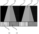
- Fig. 3 is a schematic diagram of the manufacturing process of the SNC structure in the related art.
- FIG. 4 is a schematic diagram of a semiconductor structure in an embodiment of the present disclosure.
- Fig. 5 is a flowchart of a method for manufacturing an SNC structure in an embodiment of the present disclosure.
- 6A to 6D are schematic diagrams of the process of the steps shown in FIG. 5.
- FIG. 7A and FIG. 7B are schematic diagrams of the oblique shape of the SNC structure in the embodiment of the present disclosure.
- 8A and 8B are schematic diagrams of the slant morphology of another angle section of the SNC structure in the embodiment of the present disclosure.
- FIG. 9A is one of the schematic diagrams of the undesirable effect of polysilicon growth.
- FIG. 9B is the second schematic diagram of the undesirable effect of polysilicon growth.
- FIG. 10 is a schematic diagram of the SNC structure after performing an etch-back process.
- Fig. 1 is a schematic diagram of an arrangement of the SNC structure in an exemplary embodiment of the present disclosure.
- the structure on the right side of FIG. 1 is a cross-sectional view along the position A-A of the structure shown on the left side of FIG. 1.
- the A-A position is perpendicular to the bit line (BL) and parallel to the word line (WL).
- a storage contact plug structure (SNC) 11 is located between the sidewalls of two bit line structures 12 at corresponding positions in two adjacent rows of word lines, and the bottom connects the active region 14 and the shallow trench isolation structure ( STI) 13.
- Fig. 2 is a schematic diagram of another arrangement of the SNC structure in an exemplary embodiment of the present disclosure.
- the structure on the right side of FIG. 2 is a cross-sectional view along the B-B position of the structure shown on the left side of FIG. 2.
- the B-B position is perpendicular to the word line (WL) and parallel to the bit line (BL).
- the adjacent SNC structure is isolated by the isolation structure 15 which includes a dielectric layer structure.
- the storage contact plug structure (SNC) 11 in FIG. 2 still connects the active region 14 and the shallow trench isolation structure 13 at the bottom as in FIG. 1.
- the proportions of the active region 14 and the shallow trench isolation structure 13 in the cross-section are different.
- the embodiments of the present disclosure only use the regional positions and the positions shown in FIG. 2 for simplified description. Ratio, but the present disclosure is not limited to this.
- Fig. 3 is a schematic diagram of the manufacturing process of the SNC structure in the related art.
- the isolation structure between the SNCs includes a bit line structure and a dielectric layer sidewall
- the dielectric layer sidewall needs to be formed when manufacturing the groove for accommodating the SNC structure.
- the sidewall spacers of the dielectric layer are generally hard to be formed by etching, the related technology often uses the sacrificial layer material 31 (usually oxide, such as silicon dioxide) to be etched in the BB direction as shown in FIG.
- trenches such as a
- dielectric layer structures 15 such as b
- remove the remaining sacrificial layer material 31 such as c
- deposit polysilicon between the dielectric layer structures 15 To produce SNC structure 11 (such as d).
- SNC structure 11 To produce SNC structure 11 (such as d).
- there is an isolation structure including a bit line structure such as the isolation structure 12 on the right side of FIG. 1) at the front and rear of the viewing direction in the figure, and the isolation structure including the bit line structure is usually in the dielectric layer.
- the structure 15 is formed before it is formed.
- the cross-section of the remaining sacrificial layer material is trapezoidal, that is, the final SNC structure is also a trapezoidal cross-section with a narrow upper and a wide bottom, which makes it difficult to complete good polysilicon deposition. , Often causing air gaps in the SNC structure (such as d).
- embodiments of the present disclosure provide a semiconductor structure capable of avoiding air gaps in the SNC structure.
- FIG. 4 is a schematic diagram of a semiconductor structure in an embodiment of the present disclosure.
- FIG. 4 is a cross-sectional view along the BB position of the structure shown on the left side of FIG. Isolation structure 12).
- the semiconductor structure 400 may include:
- the substrate 41 includes an active region 14 and a shallow trench isolation region 13 arranged at intervals from each other;
- the isolation structure 15 is located on the surface of the substrate 41;
- a plurality of grooves 42 are located in the isolation structure 15.
- the bottom of the grooves 42 has a first inclined surface 43, and the first inclined surface 43 is formed in the active region 14;
- the conductive plug 11 is located in the groove 42.
- FIG. 4 is a cross-sectional view in the BB direction in FIG. 2, the isolation structure 15 marked in FIG. 4 is actually a dielectric layer structure, that is, the isolation structure 15 on the right side of FIG. 2, but those skilled in the art can understand that
- the isolation structure 15 of the embodiment of the present disclosure further includes the bit line structure 12 shown in FIG. 1, and the bit line structure 12 is located in front of or behind the viewing direction of FIG. 4. That is, the isolation structure 15 of the embodiment of the present disclosure includes four sidewall structures such as two adjacent bit line structures and two adjacent dielectric layer structures, so as to realize the surrounding and isolation of the groove 42.
- the top area of the groove 42 is smaller than the bottom area, and the cross-sectional shape of the plurality of grooves may include one or more of square, polygonal, circular, or elliptical, and the plurality of grooves 42 Arranged in an array, the array can be an aligned or staggered dot array. It is understandable that since two of the opposite sidewalls of the groove 42 are formed by isolation structures including the bit line structure, and the bit line structure is perpendicular to the substrate, the length of the top surface of the groove 42 can be It is equal to the length of the bottom surface, or the width of the top surface of the groove 42 may be equal to the width of the bottom surface, which is not particularly limited in the present disclosure.
- the inclination angle of the first inclined surface 43 may be, for example, 30°-40°.
- the slope of the additional area is different from the slope of the first slope, for example, a horizontal area (for example, the bottom shape of the SNC structure 11 in the structure on the right of FIG. 1).
- the first inclined surface 43 may also be an arc surface formed by an etching process, which is not particularly limited in the present disclosure.
- FIG. 5 is a flowchart of a manufacturing method of the semiconductor structure shown in FIG. 4.
- a manufacturing method 500 of a semiconductor structure may include:
- Step S1 providing a substrate, the substrate including active regions and shallow trench isolation regions spaced apart from each other, and forming a sacrificial layer material on the surface of the substrate;
- Step S2 etching part of the sacrificial layer material to form a plurality of first grooves
- Step S3 after depositing a dielectric layer on the first groove, remove the remaining material of the sacrificial layer to form a plurality of second grooves;
- Step S4 etching down the exposed portion of the active area at the bottom of the second groove to form a first inclined surface
- Step S5 using the first inclined surface as a substrate, an epitaxial silicon growth process is performed in the second groove to fill the second groove.
- the sacrificial layer is, for example, an oxide layer, including but not limited to materials such as oxide (such as silicon dioxide), BPSG, and BSG.
- the first groove is, for example, an inverted trapezoidal groove with a wide top and a narrow bottom
- the second groove is, for example, a trapezoidal groove with a narrow bottom and a wide top.
- a non-inverted trapezoidal first groove may also be formed here, and the specific shape is determined by factors such as the process means and process conditions adopted; the second groove may also be a non-trapezoidal groove, specifically formed
- the shape is related to the shape of the first groove.
- 6A to 6D are schematic diagrams of the process of the steps shown in FIG. 5.
- FIGS. 6A to 6D are only for illustration, and are not used to limit the active regions and shallow trenches in the actual process.
- the location and proportion of the quarantine area are only for illustration, and are not used to limit the active regions and shallow trenches in the actual process.
- the embodiment of the present disclosure also etches the first trench 45 on the sacrificial layer 44 to prepare for the subsequent manufacturing of the isolation structure.
- the active region 14 and the shallow trench isolation region 13 are exposed at the bottom of the first trench 45 at the same time. Since the bit line structure located in the front or rear of the viewing direction of the figure is usually already formed at this time, the step shown in FIG. 6A is actually to fill the sacrificial layer between the bit line structures, and then etch the first groove 45 in the sacrificial layer, that is, the first groove 45 is etched in the sacrificial layer.
- the front and rear two sidewalls of the first groove 45 in the viewing direction are vertical, and are formed by an isolation structure including a bit line structure.
- the embodiment of the present disclosure also manufactures the isolation structure 15 by depositing a dielectric layer, and the material of the dielectric layer is, for example, silicon nitride.
- the embodiment of the present disclosure creates space for the manufacture of SNC by also removing the sacrificial layer 44, forming a second groove 42, and the bottom of the second groove 42 is exposed at the same time. Region 14 and shallow trench isolation region 13. It should be noted that, as can be seen from FIG. 2, the ratio of the active area exposed at the bottom of the second groove 42 to the shallow trench isolation area is actually different at different cross-sectional positions (that is, the B-B line moves laterally). Therefore, although the embodiments of the present disclosure only show one type of exposed state of the active region and the shallow trench isolation region, in practical applications, the exposed state of the active region and the shallow trench isolation region can also be multiple.
- the embodiment of the present disclosure is configured to fabricate SNC through an epitaxial silicon growth process. Therefore, for the smooth progress of the epitaxial silicon growth process, the bottom of the second groove 42 is processed, that is, through a process such as dry etching or wet etching. , Make a first inclined surface 43 at the bottom of the second groove 42.
- the bottom of the second trench 42 exposes both the active region and the shallow trench isolation region (refer to the structure on the left side of FIG. 2).
- the material of the active region is usually monocrystalline silicon
- the material of the shallow trench isolation region is usually Oxide (for example, silicon dioxide). The two provide a completely different environment for the growth of epitaxial silicon.
- single crystal silicon usually grows only on the single crystal silicon side, and it is difficult to grow on the silicon dioxide side, or grows at a very slow rate. Therefore, in order to provide more crystal orientations for the growth of single crystal silicon and make the growth of single crystal silicon more uniform and faster, the first inclined surface 43 is manufactured before the epitaxial silicon growth process in the embodiment of the present disclosure.
- the gas for etching the first inclined surface 43 may be, for example, sulfur hexafluoride (SF6), and the etching gas may be controlled by controlling parameters such as the bias voltage (Bias) and the flow rate (Flow) of the etching gas.
- the first inclined surface 43 with an inclination angle of 30°-40°. It should be noted that the etching process often cannot ensure that a perfect plane is etched. Therefore, in the actual manufacturing process, the first inclined surface 43 may also be an arc surface formed by an etching process, and the shape of the arc surface can be referred to as shown in FIG. 7A.
- the active area may also have other areas, such as a plane, that is, the end point of the first inclined surface 43 formed by etching does not coincide with the edge of the active area.
- the state of the active area can be referred to as shown in FIG. 7B.
- the shallow trench isolation region is connected to the active region, it is easy to etch the exposed portion of the shallow trench isolation region at the same time when the inclined surface is etched in the exposed portion of the active region.
- the etching selection ratio can be controlled to a value such as 1:1 to form the second inclined surface 46, and the inclination angle of the second inclined surface 46 is, for example, 20°-60°.
- the second inclined surface 46 may also be a curved surface, or the edge of the second inclined surface 46 may not coincide with the edge of the shallow trench isolation region. For these two states, please refer to FIGS. 7A and 7B respectively.
- the etching process is performed on the entire exposed portion of the active area and the entire exposed portion of the shallow trench isolation area. Therefore, the inclined surface at the bottom of the second groove 42 is actually similar to a bowl shape that is placed upright, whether it is from Viewed from the cross-section in the AA direction in FIG. 1 or from the cross-section in the BB direction in FIG. 2, there are inclined surfaces at the bottom of the second groove 42.
- the ratio of the active region 14 and the shallow trench isolation region 13 may also be different, and the slopes may be different.
- the first inclined surface 43 is cleaned in situ by means of dry cleaning of oxides, dry cleaning of removing carbon-based residues, etc., to ensure the purity of the monocrystalline silicon interface and obtain high-quality growth effects.
- the conductive plug 11 is a storage contact plug structure (SNC).
- SNC storage contact plug structure
- the selectivity of polycrystalline silicon growth can be reduced in step S4, and the growth of polycrystalline silicon can be increased at the same time. rate.
- the growth selectivity can be reduced by setting an appropriate hydrochloric acid flow rate.
- the preferred concentration of hydrochloric acid is, for example, 150 sccm ⁇ 30%.
- the shape is not easy to control, as shown in FIG. 9A or FIG. 9B.
- the polysilicon can be removed by a wet process or other etching (Recess Etch) method to leave only the single crystal silicon, and the shape of the top of the single crystal silicon can be trimmed to a rough plane (as shown in Figure 10) and adjusted The length of the conductive plug is used for the subsequent metal connection process.
- the conductive plug is a storage contact plug.
- a capacitor landing pad made of metal material can be formed on the storage contact plug for subsequent manufacturing of capacitors on the interface platform. Since the landing pad of metal material connected to the storage contact plug belongs to the manufacture of a metal-semiconductor contact structure, in another embodiment of the present disclosure, after filling the second groove, the conductive plug 11 can be Deposit metal on the surface.
- the above-mentioned landing pad is in contact with the monocrystalline silicon, and the contact conditions of the source and drain of the transistor in the peripheral circuit area are the same.
- the metal is in contact with the monocrystalline silicon.
- the metallization process can be realized, and the optimal process conditions can be reached at the same time. , Can make the process condition requirements simpler, improve the performance of the contact structure, and make the contact resistance between the metal and the single crystal silicon smaller under the condition of lower manufacturing cost.
- monocrystalline silicon is grown at the bottom of the groove to produce a storage contact plug structure (SNC structure) that fills the groove, which can avoid air in the SNC structure caused by the deposition of polysilicon in the related art.
- SNC structure storage contact plug structure
- the gap and electrical performance are reduced; in addition, by manufacturing a single crystal silicon slope at the bottom of the groove, and growing single crystal silicon on the single crystal silicon slope, the problems of uneven growth and low growth speed caused by the growth of single crystal silicon can be avoided , It can effectively improve the manufacturing efficiency while improving the yield rate.
- modules or units of the device for action execution are mentioned in the above detailed description, this division is not mandatory.
- the features and functions of two or more modules or units described above may be embodied in one module or unit.
- the features and functions of a module or unit described above can be further divided into multiple modules or units to be embodied.
- an inclined surface is provided at the exposed portion of the active area at the bottom of the groove containing the SNC structure, and polysilicon is grown inside the groove using the inclined surface as a base, which can quickly form a storage contact plug structure without air gaps and reduce component failures. Increase the yield rate.
Landscapes
- Engineering & Computer Science (AREA)
- Manufacturing & Machinery (AREA)
- Semiconductor Memories (AREA)
- Element Separation (AREA)
Abstract
一种半导体结构及其制造方法,半导体结构(400)包括:衬底(41),包括相互间隔排布的有源区(14)和浅沟槽隔离区(13);多个隔离结构(15),位于所述衬底(41)表面;多个凹槽(42),位于所述多个隔离结构(15)之间,所述凹槽(42)的底部具有第一斜面(43),所述第一斜面(43)形成于所述有源区(14);导电插塞(11),位于所述凹槽(42)中。该结构可以避免在存储接触插塞结构制造过程中在多晶硅内部形成空气隙。
Description
相关申请的交叉引用
本申请要求于2019年12月06日提交的申请号为201911239722.1、名称为“半导体结构及其制造方法”的中国专利申请的优先权,该中国专利申请的全部内容通过引用全部并入本文。
本公开涉及半导体制造技术领域,具体而言,涉及一种能够避免产生空气隙的半导体结构及其制造方法。
存储接触插塞结构(Storage Node Contact,SNC)是DRAM结构中用来连接晶体管与存储电容的接触结构,通常为多晶硅。SNC通常下部同时连接衬底和STI(Shallow Trench Isolation,浅沟槽隔离),顶部连接金属,侧壁为隔离结构的侧墙,隔离结构例如为位线结构或介质层结构。
在相关技术中,由于位线结构是先行制作好的,需要制造介质层结构作为隔离结构来制造SNC沟槽的另两个侧墙,并在沟槽中填充多晶硅以制作SNC。由于介质层侧墙硬度较大,只能通过沉积制造,因此沉积形成的介质层侧墙之间的沟槽通常为梯形结构(参考说明书图3),上窄下宽,多晶硅沉积过程中难以控制沉积的均匀度,往往会在SNC内部形成空气隙,造成SNC的电性能发生变化,产生元件故障,降低了良品率。
需要说明的是,在上述背景技术部分公开的信息仅用于加强对本公开的背景的理解,因此可以包括不构成对本领普通技术人员已知的现有技术的信息。
发明内容
本公开的目的在于提供一种半导体结构及其制造方法,用于至少在一定程度上克服由于相关技术的限制导致的存储接触插塞结构制造过程中多晶硅内部存在空气隙的问题。
根据本公开的第一方面,提供一种半导体结构,包括:
衬底,包括相互间隔排布的有源区和浅沟槽隔离区;
多个隔离结构,位于所述衬底表面;
多个凹槽,位于所述多个隔离结构之间,所述凹槽的底部具有第一斜面,所述第一斜面形成于所述有源区;
导电插塞,位于所述凹槽中。
在本公开的一种示例性实施例中,所述凹槽的顶部面积小于底部面积。
在本公开的一种示例性实施例中,所述第一斜面的倾角为30°~40°。
在本公开的一种示例性实施例中,所述凹槽的底部还具有第二斜面,所述第二斜面形成于所述浅沟槽隔离区。
在本公开的一种示例性实施例中,所述第二斜面的倾角为20°~60°。
在本公开的一种示例性实施例中,所述隔离结构包括位线结构和介质层结构。
在本公开的一种示例性实施例中,所述多个凹槽的截面包括方形、多边形、圆形或椭圆形中的一种或几种。
在本公开的一种示例性实施例中,所述多个凹槽呈阵列排布。
在本公开的一种示例性实施例中,所述第一斜面为弧面。
根据本公开的一个方面,提供一种半导体结构的制造方法,包括:
提供衬底,所述衬底包括相互间隔排布的有源区和浅沟槽隔离区;
在所述衬底表面形成牺牲层材料;
蚀刻部分所述牺牲层材料,以形成多个第一槽;
对所述第一槽沉积介质层后,去除剩余所述牺牲层材料,形成多个第二槽;
对所述第二槽的底部有源区露出部向下蚀刻以形成第一斜面;
以所述第一斜面为基底,在所述第二槽内进行外延硅生长工艺,以填充所述第二槽。
在本公开的一种示例性实施例中,所述第一斜面的倾角为30°~40°。
在本公开的一种示例性实施例中,在蚀刻所述第一斜面之后,对所述第一斜面进行自然氧化物去除处理和/或碳基残留物去除处理。
在本公开的一种示例性实施例中,所述对所述第二槽的底部有源区露出部向下蚀刻第一斜面还包括:
同时蚀刻所述有源区露出部紧邻的浅沟槽隔离结构露出部,以形成第二斜面。
在本公开的一种示例性实施例中,对所述有源区露出部和所述浅沟槽隔离结构露出部的蚀刻选择比为1:1。
在本公开的一种示例性实施例中,使用六氟化硫气体蚀刻所述斜面。
在本公开的一种示例性实施例中,所述在所述第二槽内进行外延硅生长工艺包括:
将盐酸流量设置为150sccm±30%。
在本公开的一种示例性实施例中,所述在所述第二槽内进行外延硅生长工艺包括:
在填充所述第二槽后,使用湿法工艺去除多晶硅以仅留下单晶硅,并调整填充的硅的顶部为平面。
在本公开的一种示例性实施例中,在填充所述第二槽后,还包括:
在填充的硅表面沉积金属。
本公开实施例通过在容纳SNC结构的凹槽底部的有源区露出部设置斜面,并以斜面为基底在槽内部生长多晶硅,可以快速形成不含空气隙的存储接触插塞结构,降低元件故障率,提高良品率。
应当理解的是,以上的一般描述和后文的细节描述仅是示例性和解释性的,并不能限 制本公开。
此处的附图被并入说明书中并构成本说明书的一部分,示出了符合本公开的实施例,并与说明书一起用于解释本公开的原理。显而易见地,下面描述中的附图仅仅是本公开的一些实施例,对于本领普通技术人员来讲,在不付出创造性劳动的前提下,还可以根据这些附图获得其他的附图。
图1是本公开示例性实施例中SNC结构的一种排列方式的示意图。
图2是本公开示例性实施例中SNC结构的另一种排列方式的示意图。
图3是相关技术中SNC结构的制造过程示意图。
图4是本公开实施例中一种半导体结构的示意图。
图5是本公开实施例中SNC结构制造方法的流程图。
图6A~图6D是图5所示步骤的工艺示意图。
图7A和图7B是本公开实施例中SNC结构的斜面形态示意图。
图8A和图8B是本公开实施例中SNC结构的另一个角度的剖面的斜面形态示意图。
图9A是多晶硅生长不理想效果示意图之一。
图9B是多晶硅生长不理想效果示意图之二。
图10是进行回刻蚀工艺后的SNC结构的示意图。
现在将参考附图更全面地描述示例实施方式。然而,示例实施方式能够以多种形式实施,且不应被理解为限于在此阐述的范例;相反,提供这些实施方式使得本公开将更加全面和完整,并将示例实施方式的构思全面地传达给本领的技术人员。所描述的特征、结构或特性可以以任何合适的方式结合在一个或更多实施方式中。在下面的描述中,提供许多具体细节从而给出对本公开的实施方式的充分理解。然而,本领技术人员将意识到,可以实践本公开的技术方案而省略所述特定细节中的一个或更多,或者可以采用其它的方法、组元、装置、步骤等。在其它情况下,不详细示出或描述公知技术方案以避免喧宾夺主而使得本公开的各方面变得模糊。
此外,附图仅为本公开的示意性图解,图中相同的附图标记表示相同或类似的部分,因而将省略对它们的重复描述。附图中所示的一些方框图是功能实体,不一定必须与物理或逻辑上独立的实体相对应。可以采用软件形式来实现这些功能实体,或在一个或多个硬件模块或集成电路中实现这些功能实体,或在不同网络和/或处理器装置和/或微控制器装置中实现这些功能实体。
下面结合附图对本公开示例实施方式进行详细说明。
图1是本公开示例性实施例中SNC结构的一种排列方式的示意图。
图1右侧的结构是沿着图1左侧所示结构的A-A位置的剖面图。在DRAM结构中,A-A位置垂直于位线(Bit Line,BL),平行于字线(Word Line,WL)。在图1中,存储接触插塞结构(SNC)11位于相邻两行字线中对应位置的两个位线结构12的侧墙之间,底部连接有源区14和浅沟槽隔离结构(STI)13。
图2是本公开示例性实施例中SNC结构的另一种排列方式的示意图。
图2右侧的结构是沿着图2左侧所示结构的B-B位置的剖面图。在DRAM结构中,B-B位置垂直于字线(Word Line,WL),平行于位线(Bit Line,BL),相邻的SNC结构被隔离结构15所隔离,隔离结构15包括介质层结构。可以理解的是,图2中存储接触插塞结构(SNC)11仍旧如图1中一样底部连接有源区14和浅沟槽隔离结构13。可以理解的是,移动B-B线,使剖面位置不同,有源区14和浅沟槽隔离结构13在剖面中的比例不同,本公开实施例为简化说明仅使用如图2所示的区域位置和比例,但是本公开不以此为限。
图3是相关技术中SNC结构的制造过程示意图。
参考图3,由于SNC之间的隔离结构包括位线结构和介质层侧墙,制造容纳SNC结构的凹槽时需要形成该介质层侧墙。但是由于介质层侧墙的硬度通常较大,难以通过刻蚀形成,因此,相关技术往往在图2所示的B-B方向上,通过刻蚀牺牲层材料31(通常为氧化物,如二氧化硅、BPSG、BSG等)制造沟槽(如a),使用沉积技术制造介质层结构15(如b);然后,清除剩余的牺牲层材料31(如c),在介质层结构15之间沉积多晶硅,以制造SNC结构11(如d)。可以理解的是,图中观看方向的前方和后方均存在包括位线结构在内的隔离结构(如图1右侧的隔离结构12),该包括位线结构在内的隔离结构通常在介质层结构15形成之前形成。在这种技术中,由于牺牲层材料在a步骤被刻蚀,因此剩余的牺牲层材料的剖面为梯形,即最后制造的SNC结构也为上窄下宽的梯形剖面,难以完成良好的多晶硅沉积,常常造成SNC结构中存在空气隙(如d)。
为此,本公开实施例提供了一种能够避免在SNC结构中产生空气隙的半导体结构。
图4是本公开实施例中半导体结构的示意图。
需要说明的是,图4是沿着图2左侧所示结构的B-B位置的剖面图,图中观看方向的前方和后方均存在包括位线结构在内的隔离结构(如图1右侧的隔离结构12)。
参考图4,半导体结构400可以包括:
衬底41,包括相互间隔排布的有源区14和浅沟槽隔离区13;
隔离结构15,位于衬底41表面;
多个凹槽42,位于隔离结构15中,凹槽42的底部具有第一斜面43,第一斜面43形成于有源区14;
导电插塞11,位于凹槽42中。
其中,由于图4是图2中B-B方向的剖面图,在图4中标记的隔离结构15实际上是介质层结构,即图2右侧的隔离结构15,但是本领域技术人员可以理解的是,本公开实 施例的隔离结构15还包括图1中所示的位线结构12,该位线结构12位于图4观看方向的前方或后方。即,本公开实施例的隔离结构15包括相邻的两个位线结构和相邻的两个介质层结构等四个侧墙结构,以实现对凹槽42的四周包围和隔离。
在图4所示实施例中,凹槽42的顶部面积小于底部面积,多个凹槽的截面形状可以包括方形、多边形、圆形或椭圆形中的一种或几种,多个凹槽42呈阵列排布,阵列可以为对齐的或错位的点状阵列。可以理解的是,由于凹槽42的其中两个相对的侧墙是由包括位线结构在内的隔离结构形成的,位线结构垂直于衬底,因此,凹槽42的顶面的长度可以等于底面的长度,或者,凹槽42的顶面的宽度可以等于底面的宽度,本公开对此不作特殊限制。
在本公开的一个实施例中,第一斜面43的倾角例如可以为30°~40°。当然,有源区14上还可以存在另外的区域,该另外的区域的斜率与第一斜面的斜率不同,例如为水平区域(例如图1右侧结构中SNC结构11的底部形状),在本公开的另一个实施例中,第一斜面43也可以为由蚀刻过程形成的弧面,本公开对此不做特殊限定。
图5是图4所示半导体结构的制造方法的流程图。
参考图5,半导体结构的制造方法500可以包括:
步骤S1,提供衬底,所述衬底包括相互间隔排布的有源区和浅沟槽隔离区,在衬底表面形成牺牲层材料;
步骤S2,蚀刻部分所述牺牲层材料,以形成多个第一槽;
步骤S3,对所述第一槽沉积介质层后,去除剩余所述牺牲层材料,形成多个第二槽;
步骤S4,对所述第二槽的底部有源区露出部向下蚀刻以形成第一斜面;
步骤S5,以所述第一斜面为基底,在所述第二槽内进行外延硅生长工艺,以填充所述第二槽。
其中,在本公开实施例中,所述牺牲层例如为氧化层,包括但不限于氧化物(例如二氧化硅)、BPSG、BSG等材料。该第一槽例如为上宽下窄的倒梯形槽,该第二槽例如为下窄上宽的梯形槽。本领域普通技术人员应当理解,此处也可形成非倒梯形的第一槽,具体形状由所采取的工艺手段、工艺条件等因素来确定;第二槽也可以为非梯形槽,具体形成的形状与第一槽的形状有关。
图6A~图6D是图5所示步骤的工艺示意图。
与图2和图4相同,为了简化说明,图6A~图6D中的有源区和浅沟槽隔离区的位置、比例仅为示意,并不用于限制实际制程中有源区和浅沟槽隔离区的位置、比例。
参考图6A,与图3中步骤(a)相同,本公开实施例同样在牺牲层44上刻蚀第一槽45,以为后续制造隔离结构做准备。第一槽45的底部同时露出有源区14和浅沟槽隔离区13。由于此时位于图观看方向前方或后方的位线结构通常已经形成,因此,图6A所示步骤实际是在位线结构之间填充牺牲层,然后在牺牲层中蚀刻第一槽45,即该第一槽45的观看方向的前后两个侧壁是垂直的,由包括位线结构在内的隔离结构形成。
参考图6B,与图3中步骤(b)相同,本公开实施例同样通过沉积介质层的形式制造隔离结构15,介质层的材质例如为氮化硅。
参考图6C,与图3中步骤(c)相同的是,本公开实施例通过同样清除牺牲层44来为SNC的制造创造空间,形成第二槽42,第二槽42的底部同时露出有源区14和浅沟槽隔离区13。需要说明的是,由图2可以看出,剖面位置不同(即B-B线横向移动),第二槽42底部露出的有源区和浅沟槽隔离区的比例实际是不同的。因此,本公开实施例虽然仅示出一种有源区和浅沟槽隔离区的露出状态,在实际应用中,有源区和浅沟槽隔离区的露出状态还可以为多种。
参考图6D,本公开实施例设置通过外延硅生长工艺制造SNC,因此,为了外延硅生长过程的顺利进行,对第二槽42底部做了处理,即,通过干法蚀刻或湿法蚀刻等工艺,在第二槽42底部制造第一斜面43。为了制造SNC,第二槽42的底部同时露出有源区和浅沟槽隔离区(参考图2左侧结构),有源区的材质通常为单晶硅,浅沟槽隔离区的材质通常为氧化物(例如为二氧化硅)。二者对于外延硅的生长提供了完全不同的环境。在本公开实施例中,在此过程中,单晶硅通常只在单晶硅一侧生长,在二氧化硅一侧难以生长,或者以很慢的速度生长。因此,为了为单晶硅的生长提供更多晶向,使单晶硅的生长更均匀、更迅速,本公开实施例中在外延硅生长工艺之前制造第一斜面43。
在本公开的一种示例性实施例中,蚀刻第一斜面43的气体例如可以为六氟化硫(SF6),可以通过控制蚀刻气体的偏压(Bias)、流量(Flow)等参数,蚀刻倾角为30°~40°的第一斜面43。需要说明的是,蚀刻过程往往无法保证蚀刻出完美的平面,因此实际制程中,第一斜面43还可以是由蚀刻制程形成的弧面,该弧面的形状可以参考图7A所示。此外,在一些实施例中,有源区还可能存在其他区域,例如平面,即蚀刻形成的第一斜面43的终点与有源区的边缘不重合。此时,有源区的状态可以参考图7B所示。
此外,由于浅沟槽隔离区与有源区连接,在有源区露出部蚀刻斜面时,容易同时蚀刻浅沟槽隔离区的露出部。此时,可以控制蚀刻选择比为1:1等数值,以形成第二斜面46,第二斜面46的倾角例如为20°~60°。当然,本领域相关技术人员应当理解,由于工艺的偏差或选择比非1:1,蚀刻后浅沟槽隔离区和有源区高度会有差异,但为了防止浅沟槽隔离区和有源区高度相差太大,蚀刻选择比最好不要相差过大,以免导致外延硅生长工艺时产生空气隙。与第一斜面43的形成相同,第二斜面46也可以为弧面,或者第二斜面46的边沿不与浅沟槽隔离区的边沿重合,这两种状态可以分别参见图7A和图7B。
可以理解的是,蚀刻过程是对整个有源区露出部和整个浅沟槽隔离区露出部进行的,因此,第二槽42底部的斜面实际上类似于一个正放的碗型,无论是从图1中A-A方向的剖面看,还是从图2中B-B方向的剖面看,第二槽42的底部均存在斜面。
可以参考图8A~图8B,从图1左侧A-A方向的剖面看,有源区14和浅沟槽隔离区13的比例也可以不同,斜面可以不同。
为了避免残存的杂质(自然氧化层、蚀刻残留物)(图6D中的43部位或46部位) 影响斜面的电学性能,甚至导致单晶硅生长失败,在本公开的一些实施例中,还可以通过氧化物的干法清洁、去除碳基残留物的干法清洁等方式,对第一斜面43进行原位清洁,以确保单晶硅界面的纯净度,获得高质量的生长效果。
原位清洁后,可以以斜面为基底生长单晶硅,直至控制外延硅填满整个第二槽42,以形成如图4所示的导电插塞11。在一些实施例中,导电插塞11为存储接触插塞结构(SNC)。参考图1右侧,从A-A位置剖面来看,图1右侧所示的导电插塞11(即SNC结构11)的下部也存在斜面。
需要注意的,由于生长出的单晶硅的外形往往并不理想(如图7所示),在本公开的又一个实施例中,可以在步骤S4中降低多晶硅生长的选择性,同时提高生长速率。例如,可以通过设置合适的盐酸流量来降低生长选择性。优选的盐酸浓度例如150sccm±30%。盐酸流量增加会抑制多晶的生长,更趋向于在单晶表面生长;盐酸流量减小会导致多晶硅生长速度增加,提高产量。所以既要保证单晶的质量,又要提高产量,需要找一个最合适的盐酸流量范围,因此本公开实施例设置了以上范围。
此外,由于单晶硅和多晶硅可能会同时生长,外形不容易控制,如图9A或图9B所示。此时,可以通过湿法工艺等回刻蚀(Recess Etch)方法来去除多晶硅,以仅留下单晶硅,并将单晶硅顶部的形状修整为大致平面(如图10所示)、调整导电插塞的长度,以供后续进行金属连接制程。
在一个实施例中,导电插塞为存储接触插塞。在形成存储接触插塞后,可以在存储接触插塞上形成金属材质的电容着陆垫(Landing Pad),以供后续在该界面平台上制造电容。由于在存储接触插塞上连接金属材质的着陆焊盘属于金属-半导体接触结构的制造,因此,在本公开的再一个实施例中,在填充第二槽后,还可以对导电插塞11的表面沉积金属。
此时,上述着陆焊盘与单晶硅接触,与外围电路区晶体管源极、漏极的接触情况相同,均是金属与单晶硅接触,同时实现金属化工艺,可以同时达到最优工艺条件,可以使工艺条件要求更简单,提升接触结构的性能,在制造成本更低的条件下使金属与单晶硅的接触电阻更小。
综上所述,本公开实施例通过在凹槽底部生长单晶硅,以制造填满凹槽的存储接触插塞结构(SNC结构),可以避免相关技术中沉积多晶硅导致的SNC结构中出现空气隙、电性能降低;此外,通过在凹槽底部制造单晶硅斜面,并在单晶硅斜面上生长单晶硅,可以避免单晶硅生长过程带来的生长不均匀、生长速度不高等问题,在提升良品率的同时有效提高制造效率。
应当注意,尽管在上文详细描述中提及了用于动作执行的设备的若干模块或者单元,但是这种划分并非强制性的。实际上,根据本公开的实施方式,上文描述的两个或更多模块或者单元的特征和功能可以在一个模块或者单元中具体化。反之,上文描述的一个模块或者单元的特征和功能可以进一步划分为由多个模块或者单元来具体化。
本领域技术人员在考虑说明书及实践这里公开的发明后,将容易想到本公开的其它实 施方案。本申请旨在涵盖本公开的任何变型、用途或者适应性变化,这些变型、用途或者适应性变化遵循本公开的一般性原理并包括本公开未公开的本技术领域中的公知常识或惯用技术手段。说明书和实施例仅被视为示例性的,本公开的真正范围和构思由权利要求指出。
本公开实施例通过在容纳SNC结构的凹槽底部的有源区露出部设置斜面,并以斜面为基底在槽内部生长多晶硅,可以快速形成不含空气隙的存储接触插塞结构,降低元件故障率,提高良品率。
Claims (16)
- 一种半导体结构,其特征在于,包括:衬底,包括相互间隔排布的有源区和浅沟槽隔离区;多个隔离结构,位于所述衬底表面;多个凹槽,位于所述多个隔离结构之间,所述凹槽的底部具有第一斜面,所述第一斜面形成于所述有源区;导电插塞,位于所述凹槽中。
- 如权利要求1所述的半导体结构,其特征在于,所述凹槽的顶部面积小于底部面积。
- 如权利要求1所述的半导体结构,其特征在于,所述第一斜面的倾角为30°~40°。
- 如权利要求1所述的半导体结构,其特征在于,所述凹槽的底部还具有第二斜面,所述第二斜面形成于所述浅沟槽隔离区。
- 如权利要求4所述的半导体结构,其特征在于,所述第二斜面的倾角为20°~60°。
- 如权利要求1所述的半导体结构,其特征在于,所述隔离结构包括位线结构和介质层结构。
- 如权利要求1所述的半导体结构,其特征在于,所述多个凹槽的截面包括为方形、多边形、圆形或椭圆形中的一种或几种。
- 如权利要求7所述的半导体结构,其特征在于,所述多个凹槽呈阵列排布。
- 如权利要求1所述的半导体结构,其特征在于,所述第一斜面为弧面。
- 一种半导体结构的制造方法,其特征在于,包括:提供衬底,所述衬底包括相互间隔排布的有源区和浅沟槽隔离区;在所述衬底表面形成牺牲层材料;蚀刻部分所述牺牲层材料,以形成多个第一槽;对所述第一槽沉积介质层后,去除剩余所述牺牲层材料,形成多个第二槽;对所述第二槽的底部有源区露出部向下蚀刻以形成第一斜面;以所述第一斜面为基底,在所述第二槽内进行外延硅生长工艺,以填充所述第二槽。
- 如权利要求10所述的制造方法,其特征在于,所述第一斜面的倾角为30°~40°。
- 如权利要求10所述的制造方法,其特征在于,所述对所述第二槽的底部有源区露出部向下蚀刻第一斜面还包括:同时蚀刻所述有源区露出部紧邻的浅沟槽隔离结构露出部,以形成第二斜面。
- 如权利要求12所述的制造方法,其特征在于,对所述有源区露出部和所述浅沟槽隔离结构露出部的蚀刻选择比为1:1。
- 如权利要求10所述的制造方法,其特征在于,所述在所述第二槽内进行外延硅生长工艺包括:将盐酸流量设置为150sccm±30%。
- 如权利要求10所述的制造方法,其特征在于,所述在所述第二槽内进行外延硅生 长工艺包括:在填充所述第二槽后,使用湿法工艺去除多晶硅以仅留下单晶硅,并调整填充的硅的顶部为平面。
- 如权利要求10所述的制造方法,其特征在于,在填充所述第二槽后,还包括:在填充的硅表面沉积金属。
Priority Applications (2)
| Application Number | Priority Date | Filing Date | Title |
|---|---|---|---|
| EP20896064.1A EP3968371B1 (en) | 2019-12-06 | 2020-07-16 | Semiconductor structure and manufacturing method therefor |
| US17/356,521 US20210320107A1 (en) | 2019-12-06 | 2021-06-24 | Semiconductor structure and fabrication method thereof |
Applications Claiming Priority (2)
| Application Number | Priority Date | Filing Date | Title |
|---|---|---|---|
| CN201911239722.1A CN112928094B (zh) | 2019-12-06 | 2019-12-06 | 半导体结构及其制造方法 |
| CN201911239722.1 | 2019-12-06 |
Related Child Applications (1)
| Application Number | Title | Priority Date | Filing Date |
|---|---|---|---|
| US17/356,521 Continuation US20210320107A1 (en) | 2019-12-06 | 2021-06-24 | Semiconductor structure and fabrication method thereof |
Publications (1)
| Publication Number | Publication Date |
|---|---|
| WO2021109580A1 true WO2021109580A1 (zh) | 2021-06-10 |
Family
ID=76161402
Family Applications (1)
| Application Number | Title | Priority Date | Filing Date |
|---|---|---|---|
| PCT/CN2020/102476 Ceased WO2021109580A1 (zh) | 2019-12-06 | 2020-07-16 | 半导体结构及其制造方法 |
Country Status (4)
| Country | Link |
|---|---|
| US (1) | US20210320107A1 (zh) |
| EP (1) | EP3968371B1 (zh) |
| CN (1) | CN112928094B (zh) |
| WO (1) | WO2021109580A1 (zh) |
Families Citing this family (4)
| Publication number | Priority date | Publication date | Assignee | Title |
|---|---|---|---|---|
| CN115116962B (zh) * | 2021-03-22 | 2024-06-07 | 长鑫存储技术有限公司 | 半导体结构的制备方法和半导体结构 |
| CN116130409B (zh) * | 2021-11-15 | 2026-02-17 | 长鑫存储技术有限公司 | 接触结构的形成方法、半导体结构及存储器 |
| CN115274547A (zh) * | 2022-08-26 | 2022-11-01 | 长鑫存储技术有限公司 | 半导体结构的制备方法、半导体结构及隔离结构 |
| CN117529097B (zh) * | 2023-12-28 | 2024-04-19 | 长鑫集电(北京)存储技术有限公司 | 半导体结构及其制备方法 |
Citations (4)
| Publication number | Priority date | Publication date | Assignee | Title |
|---|---|---|---|---|
| KR20090072092A (ko) * | 2007-12-28 | 2009-07-02 | 주식회사 하이닉스반도체 | 반도체 소자 및 이의 제조 방법 |
| CN208655651U (zh) * | 2018-09-19 | 2019-03-26 | 长鑫存储技术有限公司 | 埋入式字线结构及存储器 |
| CN208767278U (zh) * | 2018-10-11 | 2019-04-19 | 长鑫存储技术有限公司 | 半导体器件 |
| CN210926003U (zh) * | 2019-12-06 | 2020-07-03 | 长鑫存储技术有限公司 | 半导体结构 |
Family Cites Families (7)
| Publication number | Priority date | Publication date | Assignee | Title |
|---|---|---|---|---|
| KR101660782B1 (ko) * | 2010-07-29 | 2016-09-29 | 삼성전자주식회사 | 메모리 소자 및 이의 제조방법 |
| KR101805182B1 (ko) * | 2012-01-31 | 2017-12-06 | 에스케이하이닉스 주식회사 | 전도성 플러그를 구비하는 반도체 소자 및 그 제조 방법 |
| KR102057073B1 (ko) * | 2013-07-26 | 2019-12-18 | 에스케이하이닉스 주식회사 | 트렌치 내부에 배치되는 비트라인 구조물을 구비하는 반도체 소자, 이를 포함하는 패키지, 모듈 및 시스템 |
| US9425200B2 (en) * | 2013-11-07 | 2016-08-23 | SK Hynix Inc. | Semiconductor device including air gaps and method for fabricating the same |
| KR102509322B1 (ko) * | 2017-09-29 | 2023-03-14 | 에스케이하이닉스 주식회사 | 에어갭을 구비한 반도체장치 및 그 제조 방법 |
| KR102396583B1 (ko) * | 2017-11-09 | 2022-05-11 | 삼성전자주식회사 | 메모리 소자 및 이의 제조방법 |
| KR102476141B1 (ko) * | 2018-12-14 | 2022-12-09 | 삼성전자주식회사 | 스페이서를 포함하는 반도체 소자 및 그 제조 방법 |
-
2019
- 2019-12-06 CN CN201911239722.1A patent/CN112928094B/zh active Active
-
2020
- 2020-07-16 WO PCT/CN2020/102476 patent/WO2021109580A1/zh not_active Ceased
- 2020-07-16 EP EP20896064.1A patent/EP3968371B1/en active Active
-
2021
- 2021-06-24 US US17/356,521 patent/US20210320107A1/en not_active Abandoned
Patent Citations (4)
| Publication number | Priority date | Publication date | Assignee | Title |
|---|---|---|---|---|
| KR20090072092A (ko) * | 2007-12-28 | 2009-07-02 | 주식회사 하이닉스반도체 | 반도체 소자 및 이의 제조 방법 |
| CN208655651U (zh) * | 2018-09-19 | 2019-03-26 | 长鑫存储技术有限公司 | 埋入式字线结构及存储器 |
| CN208767278U (zh) * | 2018-10-11 | 2019-04-19 | 长鑫存储技术有限公司 | 半导体器件 |
| CN210926003U (zh) * | 2019-12-06 | 2020-07-03 | 长鑫存储技术有限公司 | 半导体结构 |
Non-Patent Citations (1)
| Title |
|---|
| See also references of EP3968371A4 * |
Also Published As
| Publication number | Publication date |
|---|---|
| CN112928094A (zh) | 2021-06-08 |
| CN112928094B (zh) | 2025-01-10 |
| US20210320107A1 (en) | 2021-10-14 |
| EP3968371A4 (en) | 2022-08-31 |
| EP3968371A1 (en) | 2022-03-16 |
| EP3968371B1 (en) | 2023-06-28 |
Similar Documents
| Publication | Publication Date | Title |
|---|---|---|
| WO2021109580A1 (zh) | 半导体结构及其制造方法 | |
| US9646990B2 (en) | NAND memory strings and methods of fabrication thereof | |
| US11462544B2 (en) | Array of recessed access gate lines | |
| TW202137518A (zh) | 三維記憶體元件及其製造方法 | |
| CN210926003U (zh) | 半导体结构 | |
| KR100455725B1 (ko) | 반도체소자의 플러그 형성방법 | |
| CN211017075U (zh) | 半导体存储器件 | |
| US8247298B2 (en) | Method of manufacturing semiconductor device | |
| US20030005881A1 (en) | Method for forming contact plug of semiconductor device | |
| WO2021232936A1 (zh) | 半导体结构及其制备方法 | |
| US20250349715A1 (en) | Semiconductor device and method for preparing semiconductor device | |
| KR20010083563A (ko) | 폴리머 부착에 의한 선택적 반구형 그레인 성장을 이용한커패시터의 형성방법 및 이에 의해 형성된 커패시터 | |
| JP2001044382A (ja) | 半導体素子のコンタクトパッド形成方法 | |
| CN210926004U (zh) | 半导体结构 | |
| US12376282B2 (en) | Semiconductor structure and method for manufacturing same | |
| CN115799161B (zh) | 半导体结构及其制备方法 | |
| CN112151363B (zh) | 具有掺杂表面的设备以及使用原位掺杂的相关方法 | |
| WO2024051061A1 (zh) | 半导体结构及其形成方法 | |
| CN110323136B (zh) | 一种FinFET制造工艺 | |
| TW202418594A (zh) | 半導體裝置 | |
| CN119560378A (zh) | 一种半导体器件的悬梁结构及其制造方法 | |
| WO2024050951A1 (zh) | 半导体结构及其形成方法 | |
| KR100755058B1 (ko) | 스텝게이트를 갖는 반도체소자 및 그 제조방법 | |
| WO2023159679A1 (zh) | 半导体结构及其制作方法 | |
| CN117790406A (zh) | 半导体结构的形成方法及半导体结构 |
Legal Events
| Date | Code | Title | Description |
|---|---|---|---|
| 121 | Ep: the epo has been informed by wipo that ep was designated in this application |
Ref document number: 20896064 Country of ref document: EP Kind code of ref document: A1 |
|
| ENP | Entry into the national phase |
Ref document number: 2020896064 Country of ref document: EP Effective date: 20211210 |
|
| NENP | Non-entry into the national phase |
Ref country code: DE |