WO2021112100A1 - 金属化フィルムおよびこれを用いたフィルムコンデンサ - Google Patents
金属化フィルムおよびこれを用いたフィルムコンデンサ Download PDFInfo
- Publication number
- WO2021112100A1 WO2021112100A1 PCT/JP2020/044746 JP2020044746W WO2021112100A1 WO 2021112100 A1 WO2021112100 A1 WO 2021112100A1 JP 2020044746 W JP2020044746 W JP 2020044746W WO 2021112100 A1 WO2021112100 A1 WO 2021112100A1
- Authority
- WO
- WIPO (PCT)
- Prior art keywords
- film
- metallized
- height
- dielectric
- maximum height
- Prior art date
- Legal status (The legal status is an assumption and is not a legal conclusion. Google has not performed a legal analysis and makes no representation as to the accuracy of the status listed.)
- Ceased
Links
Images


Classifications
-
- H—ELECTRICITY
- H01—ELECTRIC ELEMENTS
- H01G—CAPACITORS; CAPACITORS, RECTIFIERS, DETECTORS, SWITCHING DEVICES, LIGHT-SENSITIVE OR TEMPERATURE-SENSITIVE DEVICES OF THE ELECTROLYTIC TYPE
- H01G4/00—Fixed capacitors; Processes of their manufacture
- H01G4/002—Details
- H01G4/018—Dielectrics
- H01G4/06—Solid dielectrics
- H01G4/14—Organic dielectrics
- H01G4/18—Organic dielectrics of synthetic material, e.g. derivatives of cellulose
-
- B—PERFORMING OPERATIONS; TRANSPORTING
- B32—LAYERED PRODUCTS
- B32B—LAYERED PRODUCTS, i.e. PRODUCTS BUILT-UP OF STRATA OF FLAT OR NON-FLAT, e.g. CELLULAR OR HONEYCOMB, FORM
- B32B27/00—Layered products comprising a layer of synthetic resin
- B32B27/28—Layered products comprising a layer of synthetic resin comprising synthetic resins not wholly covered by any one of the sub-groups B32B27/30 - B32B27/42
-
- B—PERFORMING OPERATIONS; TRANSPORTING
- B32—LAYERED PRODUCTS
- B32B—LAYERED PRODUCTS, i.e. PRODUCTS BUILT-UP OF STRATA OF FLAT OR NON-FLAT, e.g. CELLULAR OR HONEYCOMB, FORM
- B32B27/00—Layered products comprising a layer of synthetic resin
- B32B27/06—Layered products comprising a layer of synthetic resin as the main or only constituent of a layer, which is next to another layer of the same or of a different material
- B32B27/08—Layered products comprising a layer of synthetic resin as the main or only constituent of a layer, which is next to another layer of the same or of a different material of synthetic resin
-
- B—PERFORMING OPERATIONS; TRANSPORTING
- B32—LAYERED PRODUCTS
- B32B—LAYERED PRODUCTS, i.e. PRODUCTS BUILT-UP OF STRATA OF FLAT OR NON-FLAT, e.g. CELLULAR OR HONEYCOMB, FORM
- B32B3/00—Layered products comprising a layer with external or internal discontinuities or unevennesses, or a layer of non-planar shape; Layered products comprising a layer having particular features of form
- B32B3/02—Layered products comprising a layer with external or internal discontinuities or unevennesses, or a layer of non-planar shape; Layered products comprising a layer having particular features of form characterised by features of form at particular places, e.g. in edge regions
- B32B3/08—Layered products comprising a layer with external or internal discontinuities or unevennesses, or a layer of non-planar shape; Layered products comprising a layer having particular features of form characterised by features of form at particular places, e.g. in edge regions characterised by added members at particular parts
-
- H—ELECTRICITY
- H01—ELECTRIC ELEMENTS
- H01G—CAPACITORS; CAPACITORS, RECTIFIERS, DETECTORS, SWITCHING DEVICES, LIGHT-SENSITIVE OR TEMPERATURE-SENSITIVE DEVICES OF THE ELECTROLYTIC TYPE
- H01G4/00—Fixed capacitors; Processes of their manufacture
- H01G4/002—Details
- H01G4/005—Electrodes
- H01G4/012—Form of non-self-supporting electrodes
-
- H—ELECTRICITY
- H01—ELECTRIC ELEMENTS
- H01G—CAPACITORS; CAPACITORS, RECTIFIERS, DETECTORS, SWITCHING DEVICES, LIGHT-SENSITIVE OR TEMPERATURE-SENSITIVE DEVICES OF THE ELECTROLYTIC TYPE
- H01G4/00—Fixed capacitors; Processes of their manufacture
- H01G4/32—Wound capacitors
-
- B—PERFORMING OPERATIONS; TRANSPORTING
- B32—LAYERED PRODUCTS
- B32B—LAYERED PRODUCTS, i.e. PRODUCTS BUILT-UP OF STRATA OF FLAT OR NON-FLAT, e.g. CELLULAR OR HONEYCOMB, FORM
- B32B2250/00—Layers arrangement
- B32B2250/24—All layers being polymeric
-
- B—PERFORMING OPERATIONS; TRANSPORTING
- B32—LAYERED PRODUCTS
- B32B—LAYERED PRODUCTS, i.e. PRODUCTS BUILT-UP OF STRATA OF FLAT OR NON-FLAT, e.g. CELLULAR OR HONEYCOMB, FORM
- B32B2255/00—Coating on the layer surface
- B32B2255/10—Coating on the layer surface on synthetic resin layer or on natural or synthetic rubber layer
-
- B—PERFORMING OPERATIONS; TRANSPORTING
- B32—LAYERED PRODUCTS
- B32B—LAYERED PRODUCTS, i.e. PRODUCTS BUILT-UP OF STRATA OF FLAT OR NON-FLAT, e.g. CELLULAR OR HONEYCOMB, FORM
- B32B2255/00—Coating on the layer surface
- B32B2255/20—Inorganic coating
-
- B—PERFORMING OPERATIONS; TRANSPORTING
- B32—LAYERED PRODUCTS
- B32B—LAYERED PRODUCTS, i.e. PRODUCTS BUILT-UP OF STRATA OF FLAT OR NON-FLAT, e.g. CELLULAR OR HONEYCOMB, FORM
- B32B2307/00—Properties of the layers or laminate
- B32B2307/20—Properties of the layers or laminate having particular electrical or magnetic properties, e.g. piezoelectric
- B32B2307/204—Di-electric
-
- B—PERFORMING OPERATIONS; TRANSPORTING
- B32—LAYERED PRODUCTS
- B32B—LAYERED PRODUCTS, i.e. PRODUCTS BUILT-UP OF STRATA OF FLAT OR NON-FLAT, e.g. CELLULAR OR HONEYCOMB, FORM
- B32B2307/00—Properties of the layers or laminate
- B32B2307/70—Other properties
- B32B2307/732—Dimensional properties
-
- B—PERFORMING OPERATIONS; TRANSPORTING
- B32—LAYERED PRODUCTS
- B32B—LAYERED PRODUCTS, i.e. PRODUCTS BUILT-UP OF STRATA OF FLAT OR NON-FLAT, e.g. CELLULAR OR HONEYCOMB, FORM
- B32B2457/00—Electrical equipment
- B32B2457/16—Capacitors
-
- H—ELECTRICITY
- H01—ELECTRIC ELEMENTS
- H01G—CAPACITORS; CAPACITORS, RECTIFIERS, DETECTORS, SWITCHING DEVICES, LIGHT-SENSITIVE OR TEMPERATURE-SENSITIVE DEVICES OF THE ELECTROLYTIC TYPE
- H01G4/00—Fixed capacitors; Processes of their manufacture
- H01G4/002—Details
- H01G4/005—Electrodes
- H01G4/015—Special provisions for self-healing
Definitions
- the present disclosure relates to a metallized film and a film capacitor using the metallized film.
- Patent Document 1 An example of the prior art is described in Patent Document 1.
- the metallized film of the present disclosure has a first surface and a second surface opposite to the first surface, and has a film thickness of 1 ⁇ m to 3 ⁇ m, and a metal provided on the second surface.
- the arithmetic mean height Sa1 of the first surface and the arithmetic mean height Sa2 of the second surface are different, and the maximum height Sz1 of the first surface satisfies the formula 100 nm ⁇ Sz1 ⁇ 350 nm.
- the maximum height Sz2 of the second surface satisfies the equation 10 nm ⁇ Sz2 ⁇ 100 nm.
- the film capacitor having the basic structure of the film capacitor of the present disclosure is formed by winding or laminating a plurality of metallized films formed by depositing a metal film on the surface of a dielectric film made of polypropylene resin or the like. It is formed.
- the film capacitor When a short circuit occurs in the insulation defect part of the dielectric film, the film capacitor has a self-healing property that restores the insulation of the insulation defect part by scattering the metal film around the insulation defect part by the energy of the short circuit.
- HEV hybrid electric vehicle
- EV electric vehicle
- the film capacitor since the film capacitor is hard to break down, its application has been expanded in recent years to the motor drive of a hybrid electric vehicle (HEV) or an electric vehicle (EV), an inverter system of a solar cell device, and the like.
- HEV hybrid electric vehicle
- EV electric vehicle
- the withstand voltage resistance and element processability of a film capacitor when manufacturing a film capacitor using a metallized film depends on the surface properties of the dielectric film constituting the metallized film.
- the withstand voltage resistance of the film capacitor may be lowered, or the yield when manufacturing the film capacitor may be lowered.
- the metallized film 10 of the present embodiment has a dielectric film 1 and a metal film 2.
- the dielectric film 1 has a first surface 1a and a second surface 1b opposite to the first surface 1a.
- the film thickness of the dielectric film 1 is 1 to 3 ⁇ m.
- the dielectric film 1 is made of an insulating resin.
- the resin material used for the dielectric film 1 include polypropylene (PP), polyethylene terephthalate (PET), polyphenylene sulfide (PPS), polyethylene naphthalate (PEN), polyarylate (PAR), polyphenylene ether (PPE), and the like.
- PP polypropylene
- PET polyethylene terephthalate
- PPS polyphenylene sulfide
- PEN polyethylene naphthalate
- PAR polyarylate
- PPE polyphenylene ether
- PEI polyetherimide
- cycloolefin polymers cycloolefin polymers.
- the arithmetic mean height Sa1 of the first surface 1a and the arithmetic mean height Sa2 of the second surface 1b are different.
- the arithmetic mean height Sa1 and the arithmetic mean height Sa2 may be the arithmetic mean height represented by a 10-point average.
- the maximum height Sz1 of the first surface 1a satisfies the formula 100 nm ⁇ Sz1 ⁇ 350 nm
- the maximum height Sz2 of the second surface 1b satisfies the formula 10 nm ⁇ Sz2 ⁇ 100 nm. That is, in the dielectric film 1, the maximum height Sz1 and the maximum height Sz2 are different, and the maximum height Sz1 and the maximum height Sz2 satisfy the formula 110 nm ⁇ Sz1 + Sz2 ⁇ 450 nm.
- the maximum height Sz1 and the maximum height Sz2 may be a maximum height of 10 points.
- the metal film 2 is made of a metal material and is formed on the second surface 1b of the dielectric film 1.
- the metal material used for the metal film 2 include aluminum and an alloy containing aluminum as a main component.
- the film thickness of the metal film 2 is, for example, 10 nm to 30 nm.
- the metallized film 10 is a portion where the metal film 2 is not deposited on one end side in the width direction of the dielectric film 1 (the direction perpendicular to the paper surface in FIG. 1) and the second surface 1b of the dielectric film 1 is exposed. It may have a certain metal film non-forming portion 10a.
- the metal film non-forming portion 10a may extend continuously in the length direction (left-right direction in FIG. 1) of the dielectric film.
- the metallized film 10 can be produced, for example, as follows.
- Solvents include, for example, methanol, isopropanol, n-butanol, ethylene glycol, ethylene glycol monopropyl ether, methyl ethyl ketone, methyl isobutyl ketone, xylene, propylene glycol monomethyl ether, propylene glycol monomethyl ether acetate, dimethyl acetamide, cyclohexane, toluene, or A mixture of two or more selected from these can be used.
- a base material made of PET is prepared, and one main surface (also referred to as the third surface) of the base material is blasted with alumina particles or the like.
- the third surface may have a maximum height Sz3 in a range satisfying 100 nm ⁇ Sz3 ⁇ 350 nm.
- the molding method can be appropriately selected from known methods such as a doctor blade method, a die coater method, and a knife coater method.
- the dielectric film 1 can be formed on the third surface of the base material by drying the resin solution formed on the third surface and volatilizing the solvent.
- the dielectric film 1 is peeled off from the base material, wound around a core made of resin or metal, and recovered.
- the metallized film 10 can be manufactured by depositing the metal film 2 on the second surface 1b of the recovered dielectric film 1.
- the dielectric film 1 formed on the third surface of the base material is not wound around the winding core together with the base material and recovered, but is peeled off from the base material to form a base. Separately from the material, it is wound around the core and collected. Therefore, it is possible to suppress the formation of indentations on the other main surface of the base material on the first surface 1a of the dielectric film 1.
- the first surface 1a of the dielectric film 1 on which the metal film 2 is not vapor-deposited has fine irregularities satisfying the formula 100 nm ⁇ Sz1 ⁇ 350 nm.
- the occurrence of wrinkles due to the high smoothness of the first surface 1a can be suppressed.
- the metallized film 10 is wound or laminated to produce a film capacitor, it is possible to suppress sticking of the metallized films 10 to each other and reduce the possibility that the metallized film 10 is broken. As a result, the reliability of the film capacitor provided with the metallized film 10 can be improved.
- the second surface 1b of the dielectric film 1 on which the metal film 2 is vapor-deposited satisfies the formula 10 ⁇ Sz1 ⁇ 100 nm and is smoother than the first surface 1a. That is, in the dielectric film 1, it is reduced that the film thickness is excessively lowered even in the portion where the valley of the first surface 1a and the valley of the second surface 1b overlap in a plan view. Therefore, in a film capacitor formed by laminating or winding a metallized film 10, dielectric breakdown is unlikely to occur even when a high voltage is applied.
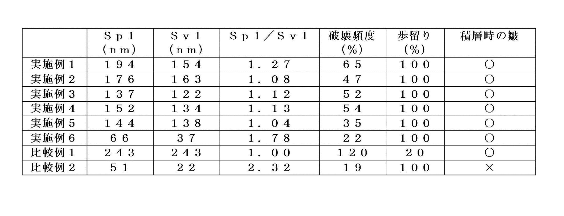
- the maximum mountain height Sp1 of the first surface 2a may be larger than the maximum valley depth Sv1.
- the slipperiness of the first surface 1a is improved, so that it is possible to suppress the occurrence of wrinkles on the metallized film 10 when manufacturing a film capacitor.
- FIG. 2 is an external perspective view showing a film capacitor according to an embodiment of the present disclosure
- FIG. 3 is a developed perspective view showing a film capacitor according to an embodiment of the present disclosure.
- the film capacitor 20 of the present embodiment includes a main body portion 3 formed by laminating a plurality of metallized films 10 and an external electrode 4 provided on the main body portion 3.
- the film capacitor 20 may have a lead wire 5 that electrically connects the external electrode 4 and an external device (not shown).
- the film capacitor 20 may have an exterior member 6 that covers the main body 3, the external electrode 4, and a part of the lead wire 5.
- the main body 3, the external electrode 4, and a part of the lead wire 5 can be electrically insulated from the external environment and protected from the external environment.
- the film capacitor 20 includes a metal film non-forming portion 10a of one metallized film 10 and a metal film non-forming portion 10a of a metallized film 10 adjacent to the one metallized film 10. May be configured to be located at different ends of the dielectric film 1 in the width direction (left-right direction in FIG. 2).
- the metallized film 10 in the film capacitor 20 it is possible to improve the yield when manufacturing the film capacitor and the withstand voltage resistance of the film capacitor. Further, according to the film capacitor 20, it is possible to prevent the adjacent metallized films 10 from coming into close contact with each other, and to secure the gas release property when a short circuit occurs in the insulation defect portion, thus improving the self-healing property. be able to.
- the film capacitor 20 may be a winding type film capacitor, for example, as shown in FIG. Even if the film capacitor 20 is a winding type film capacitor, by providing the metallized film 10, it is possible to secure the gas release property when a short circuit occurs in the insulation defect portion, so that the film capacitor 20 can be self-healing. Can be improved.
- the metallized film 10 will be described in detail based on examples.
- Example 2 A resin solution was obtained using a polyarylate resin as an organic resin and toluene as a solvent. This resin solution was applied to the blasted surface of the base material, and then dried at 80 ° C. for 1 hour to remove the solvent to obtain a dielectric film 1. The obtained dielectric film 1 was peeled off from the base material, wound around the core separately from the base material, and recovered. Next, aluminum was vapor-deposited on the second surface 1b of the recovered dielectric film 1 by a vacuum deposition method to obtain a metallized film 10 of the example.
- the metallized films of Examples 1 to 6 having different surface properties of the dielectric films are obtained by changing the combination of the organic resin and the solvent, the blasting conditions, the drying conditions of the resin solution, and the like. It was.
- Comparative Example 1 A metallized film of Comparative Example 1 was obtained in the same manner as in Example 1 except that the dielectric film and the base material were wound around the core at the same time and recovered. Further, a metallized film of Comparative Example 2 was obtained in the same manner as in Example 1 except that the surface of the base material was not blasted.
- a wide range dielectric breakdown electric field test (also referred to as a wide range BDE test) was performed for each of Examples 1 to 6 and Comparative Examples 1 and 2, and the failure frequency was calculated.
- a wide range BDE test an electric field of 300 V / ⁇ m is applied between the first surface and the second surface of the dielectric film, and the number of dielectric breakdown points per 1 m 2 is measured.
- the breakdown frequency is the number of dielectric breakdown points measured by a wide range BDE test as a percentage of the number of dielectric breakdown points at the upper limit of the standard.
- the number of dielectric breakdown points at the upper limit of the standard is the upper limit of the number of dielectric breakdown points that do not cause dielectric breakdown failure in a burn-in test in which an electric field of 210 V / ⁇ m is applied for 24 hours in an environment of 125 ° C. is there.
- the degree of wrinkling in the main body was measured when the metallized films were laminated to form the main body.
- the width dimension and the length dimension in a plan view were measured for a plurality of metallized films contained in the main body, and the ratio of the deviation between these dimensions and the predetermined dimensions of the metallized film was calculated. If the maximum value of this ratio is 2% or less, it is evaluated as ⁇ , and if it exceeds 2%, it is evaluated as x.
- the maximum height Sz1 and the maximum height Sz2 are larger than those in Examples 1 to 6, and the frequency of destruction is high. It is considered that this is because the base material and the dielectric film were wound at the same time, so that indentations on the base material were generated on the dielectric film.
- the maximum height Sz2 of the second surface 1b is smaller than that in Examples 1 to 6. Further, in Comparative Example 2, the degree of wrinkling is large when the metallized film is laminated to form the main body portion. It is considered that this is because the base material was not blasted, so that the slipperiness of the second surface of the dielectric film was reduced.
- the metallized film of the present disclosure has a first surface and a second surface opposite to the first surface, and has a film thickness of 1 ⁇ m to 3 ⁇ m, and a metal provided on the second surface.
- the arithmetic mean height Sa1 of the first surface and the arithmetic mean height Sa2 of the second surface are different, and the maximum height Sz1 of the first surface satisfies the formula 100 nm ⁇ Sz1 ⁇ 350 nm.
- the maximum height Sz2 of the second surface satisfies the equation 10 nm ⁇ Sz2 ⁇ 100 nm.
- the withstand voltage resistance of the film capacitor can be improved, and the yield at the time of manufacturing the film capacitor can be improved.
Landscapes
- Engineering & Computer Science (AREA)
- Power Engineering (AREA)
- Manufacturing & Machinery (AREA)
- Microelectronics & Electronic Packaging (AREA)
- Fixed Capacitors And Capacitor Manufacturing Machines (AREA)
Abstract
Description
実施例1~実施例6および比較例1,2のそれぞれについて、原子間力顕微鏡(AFM)を用いて、視野100μm×100μmの表面を観察し、第1面1aの算術平均高さSa1、最大高さSz1、最大山高さSp1および最大谷深さSv1、ならびに第2面1bの算術平均高さSa2および最大高さを測定した。

1a 第1面
1b 第2面
2 金属膜
2a 第1面
3 本体部
4 外部電極
5 リード線
6 外装部材
10 金属化フィルム
10a 金属膜非形成部
20 フィルムコンデンサ
Claims (3)
- 第1面および前記第1面とは反対側の第2面を有し、膜厚が1~3μmである誘電体フィルムであって、前記第1面の算術平均高さSa1と前記第2面の算術平均高さSa2とが異なり、前記第1面の最大高さSz1が下記式(1)を満たし、前記第2面の最大高さSz2が下記式(2)を満たす誘電体フィルムと、
前記第2面に設けられた金属膜と、を備える金属化フィルム。
100nm<Sz1≦350nm (1)
10nm≦Sz2≦100nm (2) - 前記最大高さSz1は、最大山高さSp1が最大谷深さSv1よりも大きい、請求項1に記載の金属化フィルム。
- 請求項1または請求項2に記載の金属化フィルムが積層または巻回されてなる本体部と、該本体部に設けられた外部電極と、を備えるフィルムコンデンサ。
Priority Applications (4)
| Application Number | Priority Date | Filing Date | Title |
|---|---|---|---|
| JP2021562670A JPWO2021112100A1 (ja) | 2019-12-02 | 2020-12-01 | |
| CN202080083464.7A CN114746265B (zh) | 2019-12-02 | 2020-12-01 | 金属化薄膜和使用该金属化薄膜的薄膜电容器 |
| EP20897412.1A EP4070945A4 (en) | 2019-12-02 | 2020-12-01 | METALLIZED FILM AND FILM CAPACITOR WITH IT |
| US17/781,459 US20230005665A1 (en) | 2019-12-02 | 2020-12-01 | Metalized film and film capacitor including metalized film |
Applications Claiming Priority (2)
| Application Number | Priority Date | Filing Date | Title |
|---|---|---|---|
| JP2019-217765 | 2019-12-02 | ||
| JP2019217765 | 2019-12-02 |
Publications (1)
| Publication Number | Publication Date |
|---|---|
| WO2021112100A1 true WO2021112100A1 (ja) | 2021-06-10 |
Family
ID=76221688
Family Applications (1)
| Application Number | Title | Priority Date | Filing Date |
|---|---|---|---|
| PCT/JP2020/044746 Ceased WO2021112100A1 (ja) | 2019-12-02 | 2020-12-01 | 金属化フィルムおよびこれを用いたフィルムコンデンサ |
Country Status (5)
| Country | Link |
|---|---|
| US (1) | US20230005665A1 (ja) |
| EP (1) | EP4070945A4 (ja) |
| JP (1) | JPWO2021112100A1 (ja) |
| CN (1) | CN114746265B (ja) |
| WO (1) | WO2021112100A1 (ja) |
Cited By (1)
| Publication number | Priority date | Publication date | Assignee | Title |
|---|---|---|---|---|
| JP2023092005A (ja) * | 2021-12-21 | 2023-07-03 | 株式会社指月電機製作所 | 金属化フィルム及びそれを用いた金属化フィルムコンデンサ |
Citations (7)
| Publication number | Priority date | Publication date | Assignee | Title |
|---|---|---|---|---|
| JPS6120180B2 (ja) | 1980-11-12 | 1986-05-21 | Mitsubishi Electric Corp | |
| JP2006269726A (ja) * | 2005-03-24 | 2006-10-05 | Matsushita Electric Ind Co Ltd | 金属化フィルムコンデンサ |
| JP2007290380A (ja) * | 2006-03-28 | 2007-11-08 | Toray Ind Inc | 金属化二軸配向ポリプロピレンフィルム及びこれからなるコンデンサ |
| JP2011122142A (ja) * | 2009-11-10 | 2011-06-23 | Toray Ind Inc | コンデンサ用二軸延伸ポリプロピレンフィルム、金属化フィルムおよびフィルムコンデンサ |
| WO2016152362A1 (ja) * | 2015-03-26 | 2016-09-29 | 京セラ株式会社 | 誘電体フィルム、およびこれを用いたフィルムコンデンサ、連結型コンデンサ、ならびにインバータ、電動車輌 |
| WO2017077752A1 (ja) * | 2015-11-05 | 2017-05-11 | 東レ株式会社 | 二軸配向ポリプロピレンフィルム、金属膜積層フィルムおよびフィルムコンデンサ |
| JP2019044171A (ja) * | 2017-08-29 | 2019-03-22 | 東レ株式会社 | ポリプロピレンフィルム、金属膜積層フィルムおよびフィルムコンデンサ |
Family Cites Families (11)
| Publication number | Priority date | Publication date | Assignee | Title |
|---|---|---|---|---|
| DE4101650A1 (de) * | 1991-01-22 | 1992-07-23 | Hoechst Ag | Biaxial gestreckte polypropylenmonofolie |
| JP2005093516A (ja) * | 2003-09-12 | 2005-04-07 | Matsushita Electric Ind Co Ltd | 金属化フィルムコンデンサ及びインバータ電源回路 |
| JP2007073574A (ja) * | 2005-09-05 | 2007-03-22 | Matsushita Electric Ind Co Ltd | 金属化フィルムコンデンサ |
| JP5338282B2 (ja) * | 2008-12-01 | 2013-11-13 | ダイキン工業株式会社 | 積層型高誘電性フィルム |
| US9805868B2 (en) * | 2012-03-28 | 2017-10-31 | Toray Industries, Inc. | Biaxially stretched polypropylene film for capacitors, metallized film, and film capacitor |
| JP2015201527A (ja) * | 2014-04-07 | 2015-11-12 | トヨタ自動車株式会社 | 金属化フィルムコンデンサ |
| KR20190109582A (ko) * | 2015-04-30 | 2019-09-25 | 오지 홀딩스 가부시키가이샤 | 콘덴서용 필름 및 그 제조 방법 |
| JP6687373B2 (ja) * | 2015-11-27 | 2020-04-22 | 京セラ株式会社 | フィルムコンデンサ、連結型コンデンサと、これを用いたインバータおよび電動車輌 |
| CN110248990A (zh) * | 2017-02-07 | 2019-09-17 | 东丽株式会社 | 双轴取向聚丙烯膜 |
| US11440292B2 (en) * | 2017-08-29 | 2022-09-13 | Toray Industries, Inc. | Polypropylene film, metal layer laminated film, and film capacitor |
| KR102563543B1 (ko) * | 2017-12-26 | 2023-08-03 | 오지 홀딩스 가부시키가이샤 | 폴리프로필렌 필름, 금속층 일체형 폴리프로필렌 필름, 필름 콘덴서 및 필름 롤 |
-
2020
- 2020-12-01 CN CN202080083464.7A patent/CN114746265B/zh active Active
- 2020-12-01 US US17/781,459 patent/US20230005665A1/en not_active Abandoned
- 2020-12-01 WO PCT/JP2020/044746 patent/WO2021112100A1/ja not_active Ceased
- 2020-12-01 JP JP2021562670A patent/JPWO2021112100A1/ja not_active Ceased
- 2020-12-01 EP EP20897412.1A patent/EP4070945A4/en not_active Withdrawn
Patent Citations (7)
| Publication number | Priority date | Publication date | Assignee | Title |
|---|---|---|---|---|
| JPS6120180B2 (ja) | 1980-11-12 | 1986-05-21 | Mitsubishi Electric Corp | |
| JP2006269726A (ja) * | 2005-03-24 | 2006-10-05 | Matsushita Electric Ind Co Ltd | 金属化フィルムコンデンサ |
| JP2007290380A (ja) * | 2006-03-28 | 2007-11-08 | Toray Ind Inc | 金属化二軸配向ポリプロピレンフィルム及びこれからなるコンデンサ |
| JP2011122142A (ja) * | 2009-11-10 | 2011-06-23 | Toray Ind Inc | コンデンサ用二軸延伸ポリプロピレンフィルム、金属化フィルムおよびフィルムコンデンサ |
| WO2016152362A1 (ja) * | 2015-03-26 | 2016-09-29 | 京セラ株式会社 | 誘電体フィルム、およびこれを用いたフィルムコンデンサ、連結型コンデンサ、ならびにインバータ、電動車輌 |
| WO2017077752A1 (ja) * | 2015-11-05 | 2017-05-11 | 東レ株式会社 | 二軸配向ポリプロピレンフィルム、金属膜積層フィルムおよびフィルムコンデンサ |
| JP2019044171A (ja) * | 2017-08-29 | 2019-03-22 | 東レ株式会社 | ポリプロピレンフィルム、金属膜積層フィルムおよびフィルムコンデンサ |
Non-Patent Citations (1)
| Title |
|---|
| See also references of EP4070945A4 |
Cited By (1)
| Publication number | Priority date | Publication date | Assignee | Title |
|---|---|---|---|---|
| JP2023092005A (ja) * | 2021-12-21 | 2023-07-03 | 株式会社指月電機製作所 | 金属化フィルム及びそれを用いた金属化フィルムコンデンサ |
Also Published As
| Publication number | Publication date |
|---|---|
| US20230005665A1 (en) | 2023-01-05 |
| JPWO2021112100A1 (ja) | 2021-06-10 |
| EP4070945A1 (en) | 2022-10-12 |
| CN114746265B (zh) | 2024-01-23 |
| CN114746265A (zh) | 2022-07-12 |
| EP4070945A4 (en) | 2024-02-21 |
Similar Documents
| Publication | Publication Date | Title |
|---|---|---|
| JP6356936B2 (ja) | フィルムコンデンサ、連結型コンデンサ、インバータおよび電動車輌 | |
| KR20090045141A (ko) | 금속화 필름 콘덴서 | |
| WO2006109732A1 (ja) | 金属化フィルムコンデンサ及びこれを用いたケースモールド型コンデンサ並びにインバータ回路及び車両駆動用モータの駆動回路 | |
| CN108028143A (zh) | 薄膜电容器、连结型电容器、逆变器以及电动车辆 | |
| CN111557038A (zh) | 薄膜电容器、连结型电容器、逆变器以及电动车辆 | |
| WO2021112100A1 (ja) | 金属化フィルムおよびこれを用いたフィルムコンデンサ | |
| JP2014107394A (ja) | 金属化フィルムコンデンサ | |
| JP6373200B2 (ja) | 高静電容量のコンデンサ用巻回型積層体、及びそれを用いた積層巻回型コンデンサ | |
| CN114041263B (zh) | 层叠型电容器、连结型电容器、逆变器以及电动车辆 | |
| JP2015103700A (ja) | フィルムコンデンサ | |
| JP5934881B2 (ja) | 金属化フィルムコンデンサ | |
| JP2015216312A (ja) | フィルムコンデンサ | |
| JP2015029005A (ja) | 誘電体フィルムおよびフィルムコンデンサ | |
| JP2017135198A (ja) | フィルムコンデンサ、連結型コンデンサ、インバータおよび電動車輌 | |
| JP7666834B2 (ja) | フィルムコンデンサ素子およびフィルムコンデンサ | |
| JP5903647B2 (ja) | 金属化フィルムコンデンサ | |
| JP2015101677A (ja) | 誘電体フィルムおよびフィルムコンデンサ | |
| JP6321419B2 (ja) | フィルムコンデンサ | |
| JP6215635B2 (ja) | 積層体およびフィルムコンデンサ | |
| JP6235291B2 (ja) | 積層体およびフィルムコンデンサ | |
| JP2023141167A (ja) | 金属化フィルムおよびこれを用いたフィルムコンデンサ | |
| JP6219637B2 (ja) | 誘電体フィルムおよびフィルムコンデンサ | |
| JP2010245153A (ja) | 金属化フィルムコンデンサおよびその製造方法 | |
| JP2023157801A (ja) | 金属化フィルムコンデンサ | |
| JP2006294789A (ja) | 金属化フィルムコンデンサ及びこれを用いたケースモールド型コンデンサ、インバータ回路、車両駆動用モータの駆動回路 |
Legal Events
| Date | Code | Title | Description |
|---|---|---|---|
| 121 | Ep: the epo has been informed by wipo that ep was designated in this application |
Ref document number: 20897412 Country of ref document: EP Kind code of ref document: A1 |
|
| ENP | Entry into the national phase |
Ref document number: 2021562670 Country of ref document: JP Kind code of ref document: A |
|
| NENP | Non-entry into the national phase |
Ref country code: DE |
|
| ENP | Entry into the national phase |
Ref document number: 2020897412 Country of ref document: EP Effective date: 20220704 |
|
| WWW | Wipo information: withdrawn in national office |
Ref document number: 2020897412 Country of ref document: EP |