WO2021117448A1 - 固体撮像装置および電子機器 - Google Patents
固体撮像装置および電子機器 Download PDFInfo
- Publication number
- WO2021117448A1 WO2021117448A1 PCT/JP2020/043090 JP2020043090W WO2021117448A1 WO 2021117448 A1 WO2021117448 A1 WO 2021117448A1 JP 2020043090 W JP2020043090 W JP 2020043090W WO 2021117448 A1 WO2021117448 A1 WO 2021117448A1
- Authority
- WO
- WIPO (PCT)
- Prior art keywords
- substrate
- solid
- image sensor
- transistor
- state image
- Prior art date
- Legal status (The legal status is an assumption and is not a legal conclusion. Google has not performed a legal analysis and makes no representation as to the accuracy of the status listed.)
- Ceased
Links
Images







Classifications
-
- H—ELECTRICITY
- H10—SEMICONDUCTOR DEVICES; ELECTRIC SOLID-STATE DEVICES NOT OTHERWISE PROVIDED FOR
- H10F—INORGANIC SEMICONDUCTOR DEVICES SENSITIVE TO INFRARED RADIATION, LIGHT, ELECTROMAGNETIC RADIATION OF SHORTER WAVELENGTH OR CORPUSCULAR RADIATION
- H10F39/00—Integrated devices, or assemblies of multiple devices, comprising at least one element covered by group H10F30/00, e.g. radiation detectors comprising photodiode arrays
- H10F39/80—Constructional details of image sensors
- H10F39/807—Pixel isolation structures
-
- H—ELECTRICITY
- H10—SEMICONDUCTOR DEVICES; ELECTRIC SOLID-STATE DEVICES NOT OTHERWISE PROVIDED FOR
- H10F—INORGANIC SEMICONDUCTOR DEVICES SENSITIVE TO INFRARED RADIATION, LIGHT, ELECTROMAGNETIC RADIATION OF SHORTER WAVELENGTH OR CORPUSCULAR RADIATION
- H10F39/00—Integrated devices, or assemblies of multiple devices, comprising at least one element covered by group H10F30/00, e.g. radiation detectors comprising photodiode arrays
- H10F39/80—Constructional details of image sensors
- H10F39/803—Pixels having integrated switching, control, storage or amplification elements
- H10F39/8037—Pixels having integrated switching, control, storage or amplification elements the integrated elements comprising a transistor
-
- H—ELECTRICITY
- H10—SEMICONDUCTOR DEVICES; ELECTRIC SOLID-STATE DEVICES NOT OTHERWISE PROVIDED FOR
- H10F—INORGANIC SEMICONDUCTOR DEVICES SENSITIVE TO INFRARED RADIATION, LIGHT, ELECTROMAGNETIC RADIATION OF SHORTER WAVELENGTH OR CORPUSCULAR RADIATION
- H10F39/00—Integrated devices, or assemblies of multiple devices, comprising at least one element covered by group H10F30/00, e.g. radiation detectors comprising photodiode arrays
- H10F39/80—Constructional details of image sensors
-
- H—ELECTRICITY
- H10—SEMICONDUCTOR DEVICES; ELECTRIC SOLID-STATE DEVICES NOT OTHERWISE PROVIDED FOR
- H10F—INORGANIC SEMICONDUCTOR DEVICES SENSITIVE TO INFRARED RADIATION, LIGHT, ELECTROMAGNETIC RADIATION OF SHORTER WAVELENGTH OR CORPUSCULAR RADIATION
- H10F39/00—Integrated devices, or assemblies of multiple devices, comprising at least one element covered by group H10F30/00, e.g. radiation detectors comprising photodiode arrays
- H10F39/80—Constructional details of image sensors
- H10F39/803—Pixels having integrated switching, control, storage or amplification elements
- H10F39/8037—Pixels having integrated switching, control, storage or amplification elements the integrated elements comprising a transistor
- H10F39/80373—Pixels having integrated switching, control, storage or amplification elements the integrated elements comprising a transistor characterised by the gate of the transistor
-
- H—ELECTRICITY
- H10—SEMICONDUCTOR DEVICES; ELECTRIC SOLID-STATE DEVICES NOT OTHERWISE PROVIDED FOR
- H10F—INORGANIC SEMICONDUCTOR DEVICES SENSITIVE TO INFRARED RADIATION, LIGHT, ELECTROMAGNETIC RADIATION OF SHORTER WAVELENGTH OR CORPUSCULAR RADIATION
- H10F39/00—Integrated devices, or assemblies of multiple devices, comprising at least one element covered by group H10F30/00, e.g. radiation detectors comprising photodiode arrays
- H10F39/80—Constructional details of image sensors
- H10F39/805—Coatings
- H10F39/8057—Optical shielding
-
- H—ELECTRICITY
- H10—SEMICONDUCTOR DEVICES; ELECTRIC SOLID-STATE DEVICES NOT OTHERWISE PROVIDED FOR
- H10F—INORGANIC SEMICONDUCTOR DEVICES SENSITIVE TO INFRARED RADIATION, LIGHT, ELECTROMAGNETIC RADIATION OF SHORTER WAVELENGTH OR CORPUSCULAR RADIATION
- H10F39/00—Integrated devices, or assemblies of multiple devices, comprising at least one element covered by group H10F30/00, e.g. radiation detectors comprising photodiode arrays
- H10F39/80—Constructional details of image sensors
- H10F39/806—Optical elements or arrangements associated with the image sensors
- H10F39/8063—Microlenses
-
- H—ELECTRICITY
- H10—SEMICONDUCTOR DEVICES; ELECTRIC SOLID-STATE DEVICES NOT OTHERWISE PROVIDED FOR
- H10F—INORGANIC SEMICONDUCTOR DEVICES SENSITIVE TO INFRARED RADIATION, LIGHT, ELECTROMAGNETIC RADIATION OF SHORTER WAVELENGTH OR CORPUSCULAR RADIATION
- H10F39/00—Integrated devices, or assemblies of multiple devices, comprising at least one element covered by group H10F30/00, e.g. radiation detectors comprising photodiode arrays
- H10F39/80—Constructional details of image sensors
- H10F39/809—Constructional details of image sensors of hybrid image sensors
-
- H—ELECTRICITY
- H10—SEMICONDUCTOR DEVICES; ELECTRIC SOLID-STATE DEVICES NOT OTHERWISE PROVIDED FOR
- H10F—INORGANIC SEMICONDUCTOR DEVICES SENSITIVE TO INFRARED RADIATION, LIGHT, ELECTROMAGNETIC RADIATION OF SHORTER WAVELENGTH OR CORPUSCULAR RADIATION
- H10F39/00—Integrated devices, or assemblies of multiple devices, comprising at least one element covered by group H10F30/00, e.g. radiation detectors comprising photodiode arrays
- H10F39/10—Integrated devices
- H10F39/12—Image sensors
- H10F39/199—Back-illuminated image sensors
-
- Y—GENERAL TAGGING OF NEW TECHNOLOGICAL DEVELOPMENTS; GENERAL TAGGING OF CROSS-SECTIONAL TECHNOLOGIES SPANNING OVER SEVERAL SECTIONS OF THE IPC; TECHNICAL SUBJECTS COVERED BY FORMER USPC CROSS-REFERENCE ART COLLECTIONS [XRACs] AND DIGESTS
- Y02—TECHNOLOGIES OR APPLICATIONS FOR MITIGATION OR ADAPTATION AGAINST CLIMATE CHANGE
- Y02P—CLIMATE CHANGE MITIGATION TECHNOLOGIES IN THE PRODUCTION OR PROCESSING OF GOODS
- Y02P70/00—Climate change mitigation technologies in the production process for final industrial or consumer products
- Y02P70/50—Manufacturing or production processes characterised by the final manufactured product
Definitions
- This disclosure relates to a solid-state image sensor and an electronic device.
- the solid-state image sensor may be manufactured using a substrate other than the ⁇ 100 ⁇ substrate.
- a substrate other than the ⁇ 100 ⁇ substrate For example, when forming a vertical trench and a horizontal trench in a semiconductor substrate, by using a ⁇ 111 ⁇ substrate as the semiconductor substrate, it becomes easy to form the vertical trench and the horizontal trench in the semiconductor substrate by etching.
- circuit elements formed on a semiconductor substrate have poor characteristics when formed on a substrate other than the ⁇ 100 ⁇ substrate, such as a ⁇ 111 ⁇ substrate.
- the present disclosure provides a solid-state image sensor and an electronic device capable of using a substrate other than the ⁇ 100 ⁇ substrate while suppressing the problem of the substrate other than the ⁇ 100 ⁇ substrate.
- the solid-state imaging device on the first side surface of the present disclosure is provided above the first substrate, which is a substrate other than the ⁇ 100 ⁇ substrate, the photoelectric conversion unit provided in the first substrate, and the first substrate.
- the first substrate which is a substrate other than the ⁇ 100 ⁇ substrate, the photoelectric conversion unit provided in the first substrate, and the first substrate.
- the first substrate includes a vertical trench extending in the vertical direction and a horizontal trench extending in the horizontal direction and connected to the vertical trench, and the horizontal trench is the first.
- a light-shielding film provided between the photoelectric conversion unit and the charge holding unit in the substrate may be included.
- the light-shielding film may be provided in the horizontal trench and the vertical trench. This makes it possible to embed a light-shielding film in the horizontal trench, for example, via the vertical trench.
- the light-shielding film may be provided in the horizontal trench and the vertical trench via an element separation insulating film. This makes it possible to embed the element separation insulating film in the horizontal trench, for example, via the vertical trench.
- the first substrate may be a ⁇ 111 ⁇ substrate
- the substrate provided with the transistor may be a ⁇ 100 ⁇ substrate or a ⁇ 110 ⁇ substrate. This makes it possible to form the transistor of the source follower circuit on the ⁇ 100 ⁇ substrate or the ⁇ 110 ⁇ substrate.
- the solid-state image sensor on the first side surface may further include a capacitor provided in the same layer as the transistor. This makes it possible, for example, to form the transistor and the capacitor of the source follower circuit with the same material.
- the solid-state image sensor on the first side surface may further include a logic circuit provided in the same layer as the transistor. This makes it possible, for example, to form the transistor of the source follower circuit and the logic circuit with the same material.
- the transistor may be an amplification transistor electrically connected to a floating diffusion portion in the first substrate. This makes it possible to use the ⁇ 111 ⁇ substrate as the first substrate while suppressing the problem of the ⁇ 111 ⁇ substrate that the characteristics of the amplification transistor deteriorate, for example.
- the transistor may include a gate insulating film and a gate electrode, which are sequentially provided on the upper surface or the lower surface of any one of the one or more substrates. This makes it possible to form a capacitor or a logic circuit with, for example, the same material as the gate insulating film of the amplification transistor and the gate electrode.
- the solid-state image sensor on the first side surface may further include a transfer transistor provided on the lower surface of the first substrate. This makes it possible, for example, to form the source follower circuit on a substrate other than the ⁇ 111 ⁇ substrate while forming the transfer transistor on the ⁇ 111 ⁇ substrate.
- the one or more substrates include a second substrate provided below the first substrate and a capacitor is provided on the lower surface, and the transistor is a lower surface of the second substrate. It may be provided in. This makes it possible to form the transistor of the source follower circuit on the substrate for the capacitor.
- the one or more substrates may further include a third substrate provided below the second substrate and provided with a logic circuit on the upper surface. This makes it possible to form the transistor of the source follower circuit on a substrate other than that for the logic circuit.
- the one or more substrates include a third substrate provided below the first substrate and provided with a capacitor and a logic circuit on the upper surface, and the transistor is the third substrate. It may be provided on the upper surface of the substrate. This makes it possible to form the transistor of the source follower circuit on the substrate for the capacitor and the logic circuit.
- the one or more substrates include a second substrate provided below the first substrate and provided with a capacitor and a logic circuit on the lower surface, and the transistor is the second substrate. It may be provided on the lower surface of the substrate. This makes it possible to form the transistor of the source follower circuit on the substrate for the capacitor and the logic circuit.
- the one or more substrates may further include a third substrate provided below the second substrate. This makes it possible to form, for example, a transistor of a source follower circuit on a substrate other than the support substrate.
- the one or more substrates include the second substrate provided below the first substrate and a capacitor provided on the lower surface, and the transistor is the second substrate. It may be provided on the lower surface. This makes it possible to form the transistor of the source follower circuit on the substrate for the capacitor.
- the one or more substrates may further include a third substrate provided below the second substrate. This makes it possible to form, for example, a transistor of a source follower circuit on a substrate other than the support substrate.
- the solid-state image sensor on the first side surface may further include a fourth substrate provided above the first substrate and having a logic circuit provided on the upper surface or the lower surface. This makes it possible to form, for example, a logic circuit on a substrate other than the support substrate.
- the fourth substrate may be provided above the first substrate via solder. This makes it possible, for example, to electrically connect the logic circuit provided on the fourth substrate to the pixels provided on the first substrate.
- the electronic device on the second side of the present disclosure is an electronic device including an image pickup device, and the image pickup device is provided on a first substrate which is a substrate other than the ⁇ 100 ⁇ substrate and in the first substrate.
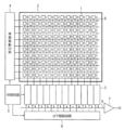
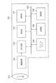
- FIG. 1 is a block diagram showing a configuration of a solid-state image sensor according to the first embodiment.
- the solid-state image sensor of FIG. 1 is a CMOS (Complementary Metal Oxide Semiconductor) type solid-state image sensor, and has a pixel array region 2 having a plurality of pixels 1, a control circuit 3, a vertical drive circuit 4, and a plurality of column signals. It includes a processing circuit 5, a horizontal drive circuit 6, an output circuit 7, a plurality of vertical signal lines 8, and a horizontal signal line 9.
- CMOS Complementary Metal Oxide Semiconductor
- Each pixel 1 includes a photodiode that functions as a photoelectric conversion unit and a plurality of pixel transistors.
- pixel transistors are MOS transistors such as transfer transistors, reset transistors, amplification transistors, and selection transistors.
- MOS transistors such as transfer transistors, reset transistors, amplification transistors, and selection transistors.
- Each pixel 1 of the present embodiment includes five MOS transistors, TRZ, TRY, TRX, TRG, and OFG, as transfer transistors.
- the pixel array area 2 has a plurality of pixels 1 arranged in a two-dimensional array.
- the pixel array region 2 is an effective pixel region that receives light and performs photoelectric conversion, amplifies and outputs the signal charge generated by the photoelectric conversion, and black for outputting optical black that serves as a reference for the black level. It includes a reference pixel area (not shown). Generally, the black reference pixel region is arranged on the outer peripheral portion of the effective pixel region.
- the control circuit 3 generates various signals that serve as reference for the operation of the vertical drive circuit 4, the column signal processing circuit 5, the horizontal drive circuit 6, etc., based on the vertical synchronization signal, the horizontal synchronization signal, and the master clock.
- the signal generated by the control circuit 3 is, for example, a clock signal or a control signal, and is input to the vertical drive circuit 4, the column signal processing circuit 5, the horizontal drive circuit 6, and the like.
- the vertical drive circuit 4 includes, for example, a shift register, and sequentially selects and scans each pixel 1 in the pixel array area 2 in the vertical direction in row units.
- the vertical drive circuit 4 further supplies a pixel signal based on the signal charge generated by each pixel 1 according to the amount of light received to the column signal processing circuit 5 through the vertical signal line 8.
- the column signal processing circuit 5 is arranged for each column of the pixel 1 in the pixel array area 2, for example, and performs signal processing of the signal output from the pixel 1 for one row based on the signal from the black reference pixel area. Do it for each row. Examples of this signal processing are noise removal and signal amplification.
- a horizontal selection switch (not shown) is provided between the output stage of the column signal processing circuit 5 and the horizontal signal line 9.
- the horizontal drive circuit 6 includes, for example, a shift register, sequentially outputs each of the column signal processing circuits 5 by sequentially outputting horizontal scanning pulses, and selects pixel signals from each of the column signal processing circuits 5 in order. Output to 9.
- the output circuit 7 performs signal processing on the signals sequentially supplied from each of the column signal processing circuits 5 through the horizontal signal line 9, and outputs the processed signal.
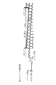
- FIG. 2 is a cross-sectional view showing the structure of the solid-state image sensor of the first embodiment.
- FIG. 2 shows a vertical cross section of one pixel 1 included in the pixel array region 2 of FIG.
- FIG. 2 shows the X-axis, Y-axis, and Z-axis that are perpendicular to each other.
- the X and Y directions correspond to the horizontal direction (horizontal direction), and the Z direction corresponds to the vertical direction (vertical direction). Further, the + Z direction corresponds to the upward direction, and the ⁇ Z direction corresponds to the downward direction.
- the ⁇ Z direction may or may not exactly coincide with the direction of gravity.
- the solid-state imaging device of the present embodiment includes a photodiode PD, a memory unit MEM, a floating diffusion unit FD, another diffusion unit OFD, a first transfer transistor TRZ, a second transfer transistor TRY (not shown), and a second.
- the transistor TR included in the above and the capacitor C are provided.
- the solid-state image sensor of the present embodiment further includes an upper substrate 11, an intermediate substrate 12, a lower substrate 13, a flattening film 14, a color filter layer 15, and an on-chip lens 16.
- the upper substrate 11 includes a substrate 21, an insulating film 22, a gate electrode 23, and an interlayer insulating film 24.
- the substrate 21 includes an N-type semiconductor region 21a, a P + type semiconductor region 21b, a P-type semiconductor region 21c, an N + type semiconductor region 21d, an N + type semiconductor region 21e, and an N + type semiconductor region 21f.
- the substrate 21 is an example of the first substrate of the present disclosure.
- the upper substrate 11 of this embodiment is a sensor substrate that functions as an image sensor.
- Reference numeral VG indicates a vertical gate electrode included in the gate electrode 23 of the first transfer transistor TRZ.
- the intermediate substrate 12 includes a substrate 31, an insulating film 32, a gate electrode 33, an interlayer insulating film 34, a multilayer wiring structure 35, an upper electrode 36, an insulating film 37, and a lower electrode 38.
- the substrate 31 includes diffusion layers 31a, 31b, and 31c.
- the substrate 31 is an example of the second substrate of the present disclosure.
- the multi-layer wiring structure 35 includes a plurality of contact plugs 35a, a wiring layer 35b, a via plug 35c, and a metal pad 35d.
- the intermediate substrate 12 of this embodiment is a capacitor substrate including the capacitor C.
- the lower substrate 13 includes a substrate 41, an insulating film 42, a gate electrode 43, an interlayer insulating film 44, and a multilayer wiring structure 45.
- the substrate 41 includes diffusion layers 41a, 41b, and 41c.
- the substrate 41 is an example of the third substrate of the present disclosure.
- the multi-layer wiring structure 45 includes a plurality of contact plugs 45a, a wiring layer 45b, a via plug 45c, and a metal pad 45d.
- the lower substrate 13 of this embodiment is a logic substrate including a logic circuit.
- the solid-state image sensor of the present embodiment further includes a trench 51, an element separation insulating film 52, a light-shielding film 53, and a plug 54.
- the trench 51 includes a vertical trench 51a and a horizontal trench 51b.
- the substrate 21 is, for example, a semiconductor substrate such as a silicon (Si) substrate.
- the substrate 21 of this embodiment is a ⁇ 111 ⁇ substrate.
- the upper surface of the substrate 21 (the surface in the + Z direction) is the back surface of the substrate 21, and the lower surface of the substrate 21 (the surface in the ⁇ Z direction) is the surface of the substrate 21. Since the solid-state image sensor of this embodiment is a back-illuminated type, the upper surface of the substrate 21 is the light incident surface of the substrate 21.
- the substrate 21 may be, for example, a substrate including a semiconductor substrate and a semiconductor layer formed on the lower surface of the semiconductor substrate.
- the ⁇ 111 ⁇ substrate is an example of a substrate other than the ⁇ 100 ⁇ substrate of the present disclosure.
- the substrate 21 includes an impurity semiconductor region such as an N-type semiconductor region 21a.
- the P + type semiconductor region 21b is provided below the N-type semiconductor region 21a.
- the P-type semiconductor region 21c is provided below the P + type semiconductor region 21b.
- the N + type semiconductor region 21d is provided in the P-type semiconductor region 21c and is located near the lower surface of the substrate 21.
- the N + type semiconductor region 21e and the N + type semiconductor region 21f are provided below the P-type semiconductor region 21c and are exposed on the lower surface of the substrate 21.
- the photodiode PD includes an N-type semiconductor region 21a and a P + type semiconductor region 21b forming a PN junction, and functions as a photoelectric conversion unit that converts received light into electric charges to generate signal charges.
- the photodiode PD is provided in the substrate 21 for each pixel 1.
- the memory unit MEM includes the N + type semiconductor region 21d and functions as a charge holding unit that holds the signal charge generated by the photodiode PD.
- the signal charge is accumulated in the N + type semiconductor region 21d.
- the floating diffusion unit FD includes the N + type semiconductor region 21e, and functions as a charge-voltage conversion unit that converts the signal charge transferred from the memory unit MEM into a voltage signal and outputs it.
- the diffusion unit OFD includes the N + type semiconductor region 21f.
- the solid-state image sensor of this embodiment employs a global shutter (GS) method, and includes a memory unit MEM in addition to a photodiode PD and a floating diffusion unit FD. Therefore, the signal charge from the photodiode PD can be supplied to the floating diffusion unit FD via the memory unit MEM.
- the solid-state image sensor of the present embodiment employs a laminated structure in which the memory unit MEM is arranged in the vertical direction instead of the horizontal direction of the photodiode PD. As a result, the area of the integrated circuit of the solid-state image sensor can be reduced.
- the insulating film 22 is provided on the lower surface of the substrate 21.
- the insulating film 22 is, for example, a silicon oxide film.
- the insulating film 22 functions as a gate insulating film of the first transfer transistor TRZ, the second transfer transistor TRY (not shown), the third transfer transistor TRX, the fourth transfer transistor TRG, and the fifth transfer transistor OFG (not shown).
- the gate electrode 23 is provided on the lower surface of the insulating film 22.
- the gate electrode 23 is, for example, a semiconductor layer such as a silicon (Si) layer, or a metal layer such as a tungsten (W) layer, an aluminum (Al) layer, a Cu (copper) layer, or a metal silicide layer.
- the gate electrode 23 is included in the first transfer transistor TRZ, the second transfer transistor TRY (not shown), the third transfer transistor TRX, the fourth transfer transistor TRG, and the fifth transfer transistor OFG (not shown).
- the gate electrode 23 of the first transfer transistor TRZ includes a vertical gate electrode VG provided in a P-type semiconductor region 21c, a P + type semiconductor region 21b, and an N-type semiconductor region 21Aa of the substrate 21 via an insulating film 22. I'm out.
- the first transfer transistor TRZ transfers the signal charge from the photodiode PD to the memory unit MEM.
- the second transfer transistor TRY and the third transfer transistor TRX transfer signal charges in the memory unit MEM.
- the fourth transfer transistor TRG transfers the signal charge from the memory unit MEM to the floating diffusion unit FD.
- the fifth transfer transistor OFG is provided between the photodiode PD and the diffuser OFD, and is used to initialize the photodiode PD, that is, to reset the potential of the photodiode PD to the power supply potential (VDD potential). Will be done.
- the semiconductor device of the present embodiment may include only the third transfer transistor TRX among the second transfer transistor TRY and the third transfer transistor TRX. When the semiconductor device includes TRY and TRX, the signal charge transfer performance is better, but when the semiconductor device includes only TRX, the structure of the semiconductor device becomes simple.
- the interlayer insulating film 24 is formed on the lower surface of the substrate 21 so as to cover the insulating film 22, the gate electrode 23, and the like.
- the interlayer insulating film 24 is, for example, a silicon oxide film or a laminated film including a silicon oxide film.
- the substrate 31 is provided below the substrate 21 via an interlayer insulating film 24, and is in contact with the lower surface of the interlayer insulating film 24.
- the substrate 31 is, for example, a semiconductor substrate such as a silicon substrate.
- the substrate 31 of the present embodiment has a crystal plane different from the crystal plane of the substrate 21.
- the substrate 31 of the present embodiment is a semiconductor substrate other than the ⁇ 111 ⁇ substrate, for example, a ⁇ 100 ⁇ substrate.
- the substrate 31 may be a ⁇ 110 ⁇ substrate.
- the upper surface of the substrate 31 is the back surface of the substrate 31, and the lower surface of the substrate 31 is the surface of the substrate 31.
- the substrate 31 may be, for example, a substrate including a semiconductor substrate and a semiconductor layer formed on the lower surface of the semiconductor substrate.
- the insulating film 32 is provided on the lower surface of the substrate 31.
- the insulating film 32 is, for example, a silicon oxide film.
- the insulating film 32 functions as a gate insulating film of a reset transistor RST (not shown), an amplification transistor AMP, a selection transistor SEL (not shown), and an upper dielectric film of a capacitor C.
- the gate electrode 33 is provided on the lower surface of the insulating film 32.
- the gate electrode 33 is, for example, a semiconductor layer such as a silicon layer, or a metal layer such as a tungsten layer, an aluminum layer, a copper layer, or a metal silicide layer.
- the gate electrode 33 is included in a reset transistor RST (not shown), an amplification transistor AMP, and a selection transistor SEL (not shown).
- the reset transistor RST is used to initialize the memory unit MEM and the floating diffusion unit FD, that is, to reset the potentials of the memory unit MEM and the floating diffusion unit FD to the power supply potential (VDD potential).
- the amplification transistor AMP functions as an input unit of a source follower circuit that reads a voltage signal from the floating diffusion unit FD.
- the diffusion layers 31a and 31b in the substrate 31 function as a drain region and a source region of the amplification transistor AMP.
- the gate electrode 33 of the amplification transistor AMP is electrically connected to the floating diffusion portion FD.
- the diffusion layer 31b is electrically connected to the logic circuit in the lower substrate 13.
- the amplification transistor AMP of the present embodiment has a constant current electrically connected to the vertical signal line 8 by electrically connecting its source region to the vertical signal line 8 (FIG. 1) via the selection transistor SEL.
- a source follower circuit is constructed together with the source.
- the amplification transistor AMP is an example of a transistor included in the source follower circuit of the present disclosure.
- the selection transistor SEL is used to select the corresponding pixel 1.
- the selection transistor SEL is turned on, the corresponding pixel 1 changes to the selected state, and the pixel signal from the amplification transistor AMP is read out by the column signal processing circuit 5 (FIG. 1) via the vertical signal line 8.
- the upper electrode 36, the insulating film 37, and the lower electrode 38 are provided on the lower surface of the insulating film 32 in this order.
- the upper electrode 36 is, for example, a semiconductor layer such as a silicon layer, or a metal layer such as a tungsten layer, an aluminum layer, a copper layer, or a metal silicide layer.
- the gate electrode 33 and the upper electrode 36 of the present embodiment are included in the same electrode layer, and are formed by forming the electrode layer on the surface of the insulating film 32 and processing the electrode layer by etching.
- the insulating film 37 is, for example, a silicon oxide film, and functions as a lower dielectric film of the capacitor C.
- the lower electrode 38 is, for example, a semiconductor layer such as a silicon layer, or a metal layer such as a tungsten layer, an aluminum layer, a copper layer, or a metal silicide layer.
- the upper electrode 36, the insulating film 37, and the lower electrode 38 may be provided below the substrate 31 at positions different from those shown in FIG.
- the capacitor C includes three electrodes, a diffusion layer 31c, an upper electrode 36, and a lower electrode 38, and two dielectric films, an insulating film 32 and an insulating film 37, sandwiched between these electrodes.
- the capacitor C of the present embodiment is provided on the lower surface of the substrate 31, and the amplification transistor AMP of the present embodiment is also provided on the lower surface of the substrate 31.
- the amplification transistor AMP and the capacitor C of the present embodiment are provided in the same layer.
- the gate insulating film (insulation film 32) and the gate electrode 33 of the amplification transistor AMP are each an upper dielectric film of the capacitor C. It is provided in the same layer as the (insulating film 32) and the upper electrode 36.
- the capacitor C of the present embodiment is used, for example, as the pixel internal capacity of the corresponding pixel 1.
- the interlayer insulating film 34 is formed on the lower surface of the substrate 31 so as to cover the insulating film 32, the gate electrode 33, the upper electrode 36, the insulating film 37, the lower electrode 38, and the like.
- the interlayer insulating film 34 is, for example, a silicon oxide film or a laminated film including a silicon oxide film.
- the multilayer wiring structure 35 is provided in the interlayer insulating film 34, and includes a plurality of contact plugs 35a, a wiring layer 35b, a via plug 35c, and a metal pad 35d.
- the contact plug 35a is provided on the lower surfaces of the diffusion layers 31a, 31b, 31c, the gate electrode 33, the upper electrode 36, the lower electrode 38, and the like.
- the wiring layer 35b includes a plurality of wirings provided under these contact plugs 35a.
- the via plug 35c is provided below the wiring layer 35b.
- the metal pad 35d is provided under the via plug 35c and is joined to the metal pad 45d of the lower substrate 13. As a result, the intermediate substrate 12 and the lower substrate 13 are electrically connected via these metal pads 35d and 45d.
- the substrate 41 is provided below the substrate 31 via the interlayer insulating films 34 and 44.
- the substrate 41 is, for example, a semiconductor substrate such as a silicon substrate.
- the substrate 41 of the present embodiment has a crystal plane different from the crystal plane of the substrate 21.
- the substrate 41 of the present embodiment is a semiconductor substrate other than the ⁇ 111 ⁇ substrate, for example, a ⁇ 100 ⁇ substrate.
- the substrate 41 may be a ⁇ 110 ⁇ substrate.
- the upper surface of the substrate 41 is the front surface of the substrate 41
- the lower surface of the substrate 41 is the back surface of the substrate 41.
- the substrate 41 may be, for example, a substrate including a semiconductor substrate and a semiconductor layer formed on the lower surface of the semiconductor substrate.
- the substrate 41 of the present embodiment functions as a support substrate that supports the substrate 21 and the substrate 31.
- the insulating film 42 is provided on the upper surface of the substrate 41.
- the insulating film 42 is, for example, a silicon oxide film.
- the insulating film 42 functions as a gate insulating film of the transistor TR included in the logic circuit.
- the gate electrode 43 is provided on the upper surface of the insulating film 42.
- the gate electrode 43 is, for example, a semiconductor layer such as a silicon layer, or a metal layer such as a tungsten layer, an aluminum layer, a copper layer, or a metal silicide layer.
- the gate electrode 43 is included in the transistor TR included in the logic circuit.
- the lower substrate 13 of the present embodiment includes a logic circuit provided on the upper surface of the substrate 41, and the transistor TR shown in FIG. 2 constitutes this logic circuit.
- This logic circuit functions, for example, to control various operations of the solid-state image sensor.
- the diffusion layers 41a and 41b in the substrate 41 function as a drain region and a source region of the transistor TR.
- the interlayer insulating film 44 is formed on the upper surface of the substrate 41 so as to cover the insulating film 42, the gate electrode 43, and the like, and is in contact with the lower surface of the interlayer insulating film 34.
- the interlayer insulating film 44 is, for example, a silicon oxide film or a laminated film including a silicon oxide film.
- the multilayer wiring structure 45 is provided in the interlayer insulating film 44, and includes a plurality of contact plugs 45a, a wiring layer 45b, a via plug 45c, and a metal pad 45d.
- the contact plug 45a is provided on the upper surfaces of the diffusion layers 41a, 41b, 41c, the gate electrode 43, and the like.
- the wiring layer 45b includes a plurality of wirings provided on these contact plugs 45a.
- the via plug 45c is provided on the wiring layer 45b.
- the metal pad 45d is provided on the via plug 45c and is joined to the metal pad 35d of the intermediate substrate 12. As a result, the intermediate substrate 12 and the lower substrate 13 are electrically connected via these metal pads 35d and 45d.
- the trench 51 includes a vertical trench 51a provided in the substrate 21 and extending in the vertical direction (Z direction) and a horizontal trench 51b provided in the substrate 21 and extending in the horizontal direction (X direction).
- the vertical trench 51a extends in the vertical direction from the upper surface of the wiring layer 35b through the lower surface of the substrate 21, and the horizontal trench 51b is connected to the vertical trench 51a and extends in the horizontal direction from the vertical trench 51a. ..
- the vertical trench 51a has a plate-like shape that extends in the YZ plane.
- the lateral trench 51b has a plate-like shape that expands in the XY plane, and is provided between the photodiode PD and the memory unit MEM, or between the photodiode PD and the stray diffusion unit FD. ..
- the element separation insulating film 52 is embedded in the trench 51 and is formed on the side surface, the upper surface, and the lower surface of the trench 52.
- the element separation insulating film 52 functions as a film for electrically separating the pixels 1 from each other.
- the element separation insulating film 13 is, for example, a silicon oxide film.
- the element separation insulating film 52 of the present embodiment is formed in both the vertical trench 51a and the horizontal trench 41b.
- the light-shielding film 53 is embedded in the trench 51 like the element separation insulating film 52, and is formed on the side surface, the upper surface, and the lower surface of the trench 51 via the element separation insulating film 52.
- the light-shielding film 53 shields light from the upper surface of the substrate 21 and functions as a film for optically separating the photodiode PD and the memory unit MEM.
- the light-shielding film 53 is, for example, a metal layer such as a tungsten layer or a compound semiconductor layer having a chalcopyrite structure having a high extinction coefficient.
- the plug 54 is provided in the upper substrate 11 and the intermediate substrate 12 so as to electrically connect the floating diffusion portion FD and the wiring in the wiring layer 35b. As a result, the floating diffusion unit FD and the gate electrode 33 of the amplification transistor AMP are electrically connected.
- the plug 54 is provided in the substrate 31 via an insulating film ⁇ .
- the flattening film 14 is formed on the entire surface of the substrate 21 so as to cover the upper surface of the substrate 21, whereby the surface on the upper surface of the substrate 21 is flat.
- the flattening film 14 is, for example, an organic film such as a resin film.
- the flattening film 14 may be an insulating film other than the organic film, and the upper surface of the insulating film may be flattened by CMP (Chemical Mechanical Polishing).
- the color filter layer 15 is formed on the flattening film 14 for each pixel 1.
- a color filter layer 15 for red (R), green (G), or blue (B) is arranged above the photodiode PD of pixel 1 in red, green, or blue.
- the color filter layer 15 may be arranged above the photodiode PD of the pixel 1 of the infrared light as the color filter layer 15 for infrared light.
- the color filter layer 15 has a property of being able to transmit light having a predetermined wavelength, and the light transmitted through the color filter layer 15 is incident on the photodiode PD via the flattening film 14.
- the on-chip lens 16 is formed on the color filter layer 15 for each pixel 1.
- the on-chip lens 16 has a property of condensing the incident light, and the light collected by the on-chip lens 16 is incident on the photodiode PD via the color filter layer 15 and the flattening film 14. ..
- the substrate 21 of this embodiment is not a ⁇ 100 ⁇ substrate but a ⁇ 111 ⁇ substrate.
- some circuit elements of the solid-state image pickup device have poor characteristics when formed on the ⁇ 111 ⁇ substrate.
- An example of such a circuit element is an amplification transistor AMP included in a source follower circuit. Therefore, in the present embodiment, such a circuit element is formed not on the substrate 21 which is the ⁇ 111 ⁇ substrate but on the substrate 31 which is the ⁇ 100 ⁇ substrate. Therefore, according to the present embodiment, it is possible to use the ⁇ 111 ⁇ substrate while suppressing the problem of the ⁇ 111 ⁇ substrate that the characteristics of the circuit element deteriorate.
- a specific example of this will be described in detail.
- the solid-state image sensor of the present embodiment employs the global shutter (GS) method, and includes a memory unit MEM in addition to the photodiode PD and the floating diffusion unit FD. Therefore, the signal charge from the photodiode PD can be supplied to the floating diffusion unit FD via the memory unit MEM.
- the solid-state image sensor of the present embodiment employs a laminated structure in which the memory unit MEM is arranged in the vertical direction instead of the horizontal direction of the photodiode PD. As a result, the area of the integrated circuit of the solid-state image sensor can be reduced.
- a light-shielding film 53 extending in the lateral direction is formed between the photodiode PD and the memory unit MEM, and the photodiode PD and the memory unit MEM are optically connected by the light-shielding film 53. It is desirable to separate into. Therefore, in the present embodiment, a vertical trench 51a extending in the vertical direction is formed in the substrate 21, and a horizontal trench 51b extending in the horizontal direction is formed from the vertical trench 51a, thereby forming a horizontal trench 51b between the photodiode FD and the memory unit MEM. It forms a transverse trench 51b.
- the light-shielding film 53 is formed in the horizontal trench 51b. Since the vertical trench 51a of the present embodiment is formed to form an element separation portion that electrically separates the pixels 1 from each other, in the present embodiment, the vertical trench 51a and the horizontal trench 51b are separated and insulated from each other. The light-shielding film 53 is embedded via the film 52.
- the substrate 21 is a ⁇ 111 ⁇ substrate. This facilitates the formation of the vertical trench 51a and the horizontal trench 51b in the substrate 21 by etching.
- the substrate 21 is a ⁇ 111 ⁇ substrate, the plurality of ⁇ 110> directions and the plurality of ⁇ 112> directions in the substrate 21 are perpendicular to the Z direction.
- the substrate 21 is easily etched in the X direction because a long distance in the substrate 21 is etched in the X direction, that is, the etching rate in the X direction is high. High is desirable.
- the ⁇ 111 ⁇ substrate has a high etching rate in the ⁇ 110> direction. Therefore, according to the present embodiment, the lateral trench 51b can be easily formed in the substrate 21 by making the X direction parallel to the ⁇ 110> direction.
- the interface state of the ⁇ 111 ⁇ substrate is not suitable as compared with the ⁇ 100 ⁇ substrate and the ⁇ 110 ⁇ substrate. Therefore, if the amplification transistor AMP of the source follower circuit is provided on the substrate 21 which is the ⁇ 111 ⁇ substrate, the S / N ratio (signal / noise ratio) in the source follower circuit deteriorates.
- the amplification transistor AMP of the present embodiment is provided not on the substrate 21 which is the ⁇ 111 ⁇ substrate but on the substrate 31 which is the ⁇ 100 ⁇ substrate. As a result, deterioration of the S / N ratio in the source follower circuit can be suppressed. As described above, according to the present embodiment, it becomes easier to form the vertical trench 51a and the horizontal trench 51b while suppressing the disadvantage of the ⁇ 111 ⁇ substrate that the S / N ratio in the source follower circuit deteriorates. It is possible to enjoy the merits of the substrate.
- the substrate 31 on which the amplification transistor AMP is provided may be a substrate other than the ⁇ 100 ⁇ substrate as long as it is a substrate other than the ⁇ 111 ⁇ substrate.
- the substrate 31 may be, for example, a ⁇ 110 ⁇ substrate.
- using the substrate 31 as a ⁇ 100 ⁇ substrate has an advantage that the cost of the substrate 31 can be suppressed.
- the amplification transistor AMP may be provided on the substrate 41 instead of the substrate 31.
- the substrate 41 may be a substrate other than the ⁇ 100 ⁇ substrate as long as it is a substrate other than the ⁇ 111 ⁇ substrate. This is the same as in the case of the substrate 31.
- the Si ⁇ 111 ⁇ substrate in the present disclosure is a substrate or wafer made of a silicon single crystal and having a crystal plane represented by ⁇ 111 ⁇ in the Miller index notation.
- the Si ⁇ 111 ⁇ substrate in the present disclosure also includes a substrate or wafer whose crystal orientation is deviated by several degrees, for example, a substrate or wafer deviated by several degrees from the ⁇ 111 ⁇ plane in the closest [110] direction. Further, it also includes a silicon single crystal grown on a part or the entire surface of these substrates or wafers by an epitaxial method or the like.
- the ⁇ 111 ⁇ planes are crystal planes equivalent to each other in terms of symmetry, which are (111) plane, (-111) plane, (1-11) plane, (11-1) plane, and (-) plane. It is a general term for the 1-11) plane, the (-11-1) plane, the (1-1-1) plane, and the (1-1-1) plane. Therefore, the description of the Si ⁇ 111 ⁇ substrate in the specification and the like of the present disclosure may be read as, for example, a Si (1-11) substrate.
- the bar sign for expressing the negative index of the Miller index is replaced with a minus sign.
- the ⁇ 110> direction in the description of the present disclosure is the [110] direction, the [101] direction, the [011] direction, the [-110] direction, and [1-10], which are crystal plane directions equivalent to each other in terms of symmetry.
- Direction, [-101] direction, [10-1] direction, [0-11] direction, [01-1] direction, [-1-10] direction, [-10-1] direction and [0-1- 1] It is a general term for directions, and may be read as either.
- etching is performed in a direction orthogonal to the element forming surface and a direction further orthogonal to the direction orthogonal to the element forming surface (that is, a direction parallel to the element forming surface).
- FIG. 18 shows a specific combination of a plane and an orientation in which etching in the ⁇ 110> direction is established on the ⁇ 111 ⁇ plane, which is the crystal plane of the Si ⁇ 111 ⁇ substrate in the present disclosure. ..
- the ⁇ 110> direction of the present disclosure is limited to a direction orthogonal to the ⁇ 111 ⁇ plane which is an element forming surface and a direction parallel to the element forming surface. That is, the combination of the element forming surface of the Si ⁇ 111 ⁇ substrate of the present disclosure and the orientation for etching the Si ⁇ 111 ⁇ substrate is selected from any of the combinations shown by ⁇ in FIG.
- the case where the etching proceeds in the X-axis direction but does not proceed in the Y-axis direction and the Z-axis direction is illustrated by using the Si ⁇ 111 ⁇ substrate.
- the present disclosure is not limited to this, and it is sufficient that the etching progress direction is in both the X-axis direction and the Y-axis direction, or in either the X-axis direction or the Y-axis direction.
- the horizontal shading portion has one or two Si backbonds in a direction substantially horizontal to the substrate surface, at least three, whereas three Si backbonds are substantially perpendicular to the substrate surface.
- the back bond is described, for example, by taking FIG. 19 as an example.
- the Si unbonded hand side is the positive direction with respect to the normal of the Si ⁇ 111 ⁇ plane
- the back bond represents a bond extending in the negative direction on the opposite side. ..
- FIG. 19 shows an example of three back bonds at -19.47 ° to + 19.47 ° with respect to the ⁇ 111 ⁇ plane.
- the horizontal light-shielding portion is orthogonal to the first direction and is represented by a plane index ⁇ 111 ⁇ .
- ⁇ Along the first plane along the first crystal plane of the substrate and along the second crystal plane of the Si ⁇ 111 ⁇ substrate that is inclined with respect to the first direction and represented by a plane index ⁇ 111 ⁇ .
- the Si ⁇ 111 ⁇ substrate includes, for example, a substrate in which the surface of the substrate is processed so as to have an off angle with respect to the ⁇ 112> direction, as shown in FIG.
- the off angle is 19.47 ° or less, even in the case of a substrate having an off angle, the etching rate in the ⁇ 111> direction, that is, the direction having three Si back bonds, is in the ⁇ 110> direction, that is, Si back.
- the relationship in which the etching rate in the direction of having one bond is sufficiently high is maintained.
- the off angle increases, the number of steps increases and the density of microsteps increases, so 5 ° or less is preferable. In the example of FIG.
- the Si plane orientation can be analyzed by using an X-ray diffraction method, an electron beam diffraction method, an electron backscatter diffraction method, or the like. Since the number of Si backbonds is determined by the Si product structure, the number of backbonds can also be analyzed by analyzing the Si plane orientation.
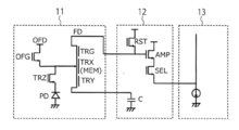
- FIG. 3 is a circuit diagram showing the configuration of the solid-state image sensor of the first embodiment.
- FIG. 3 shows various circuit elements provided in the upper substrate 11, the intermediate substrate 12, and the lower substrate 13.
- the upper substrate 11 includes a photodiode PD, a memory unit MEM, a floating diffusion unit FD, a diffusion unit OFD, a first transfer transistor TRZ, a second transfer transistor TRY, a third transfer transistor TRX, and a fourth transfer. It includes a transistor TRG and a fifth transfer transistor OFG.
- the intermediate substrate 12 includes a reset transistor RST, an amplification transistor AMP, a selection transistor SEL, and a capacitor C.
- the lower substrate 13 includes a constant current source as shown in FIG.
- the fourth transfer transistor TRG, the third transfer transistor TRX, and the second transfer transistor TRY are arranged in series between the floating diffusion unit FD and the capacitor C, and are provided in the vicinity of the memory unit MEM.
- One main terminal of the first transfer transistor TRZ is connected to the cathode of the photodiode PD, and the other main terminal of the first transfer transistor TRZ is provided near the memory unit MEM and the third transfer transistor TRX.
- One main terminal of the fifth transfer transistor OFG is connected to the diffusion unit OFD, and the other main terminal of the fifth transfer transistor OFG is provided near the memory unit MEM and the third transfer transistor TRX.
- the reset transistor RST includes a source terminal connected to the floating diffusion unit FD and a drain terminal connected to the power supply wiring (VDD wiring).
- the amplification transistor AMP has a source terminal of the floating diffusion section FD, a gate terminal connected to the floating diffusion section FD, a drain terminal connected to the power supply wiring (VDD wiring), and a source terminal connected to the selection transistor SEL. I have.
- the amplification transistor AMP and the selection transistor SEL are arranged in series between the power supply wiring (VDD wiring) and the constant current source.
- the amplification transistor AMP is sourced together with this constant current source electrically connected to the vertical signal line 8 by electrically connecting its source terminal to the vertical signal line 8 (FIG. 1) via the selection transistor SEL. Configure a follower circuit.
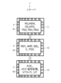
- FIG. 4 is a plan view schematically showing the structure of the solid-state image sensor of the first embodiment.
- FIG. 4 schematically shows the planar configuration of the upper substrate 11, the intermediate substrate 12, and the lower substrate 13.
- Reference numeral P represents a pad electrode.
- Reference numeral A1 is a photodiode PD, a memory unit MEM, a floating diffusion unit FD, a diffusion unit OFD, a first transfer transistor TRZ, a second transfer transistor TRY (not shown), a third transfer transistor TRX, and a third in the upper substrate 11.
- Reference numeral A2 represents a region in which the reset transistor RST, the amplification transistor AMP, the selection transistor SEL, the capacitor C, the FDG (conversion gain switching unit), and the like are arranged in the intermediate substrate 12.
- Reference numeral A3 represents an area in the lower substrate 13 in which logic circuits such as an ADC (analog-to-digital conversion unit), a memory / signal processing unit, a V driver, and an I / F (interface) are arranged.
- the pad electrode P of the present embodiment is arranged around the region A1, around the region A2, and around the region A3.
- the amplification transistor AMP of this embodiment is arranged not in the region A1 of the upper substrate 11 but in the region A2 of the intermediate substrate 12. As a result, the amplification transistor AMP can be provided on a substrate other than the ⁇ 111 ⁇ substrate, and deterioration of the S / N ratio in the source follower circuit can be suppressed. Furthermore, by arranging the amplification transistor AMP in the region A2, the area of the region A1 can be reduced.
- the amplification transistor AMP of the present embodiment is arranged not in the region A3 of the lower substrate 13 but in the region A2 of the intermediate substrate 12. This makes it possible to suppress the expansion of the area of the region A3 due to the amplification transistor AMP.
- the amplification transistor AMP of this embodiment is arranged in the region A2 of the intermediate substrate 12.
- the area of the region A2 is set to be about the same as the area of the region A1 or the area of the region A3, a circuit element other than the amplification transistor AMP can be arranged in the region A2. Therefore, in the present embodiment, the reset transistor RST, the selection transistor SEL, the capacitor C, and the FDG are arranged in the region A2. According to this embodiment, the amount of saturated charge can be increased by arranging the capacitor C, which is the internal capacitance of the pixel, in the region A2.
- the amplification transistor AMP in the region A2, it is possible to reduce the area of the region A1 and the area of the region A3.
- the area of the region A2 By setting the area of the region A2 to be about the same as the area of the region A1 and the area of the region A3, it is possible to reduce the area of the integrated circuit of the solid-state image sensor of the present embodiment.
- the photodiode PD of the present embodiment is provided in the substrate 21 which is a substrate other than the ⁇ 100 ⁇ substrate, and the amplification transistor AMP of the present embodiment has a crystal plane different from the crystal plane of the substrate 21. It is provided on the substrate 31. Therefore, according to the present embodiment, it is possible to use a substrate other than the ⁇ 100 ⁇ substrate while suppressing the problem of the substrate other than the ⁇ 100 ⁇ substrate (for example, the ⁇ 111 ⁇ substrate).
- FIG. 5 is a cross-sectional view showing the structure of the solid-state image sensor of the second embodiment.
- the solid-state image sensor of this embodiment includes an upper substrate 11 and a lower substrate 13, but does not include an intermediate substrate 12.
- the upper substrate 11 includes a multi-layer wiring structure 25 in addition to the components shown in FIG.
- the multilayer wiring structure 25 is provided in the interlayer insulating film 24, and includes a contact plug 25a, a wiring layer 25b, a via plug 25c, and a metal pad 25d.
- the contact plug 25a is provided on the lower surface of the floating diffusion portion FD.
- the wiring layer 25b includes a plurality of wirings such as wirings provided under the contact plug 25a.
- the via plug 25c is provided below the wiring layer 25b.
- the metal pad 25d is provided under the via plug 25c and is joined to the metal pad 45d of the lower substrate 13. As a result, the upper substrate 11 and the lower substrate 13 are electrically connected via these metal pads 25d and 45d.
- the vertical trench 51a extends in the vertical direction from the upper surface of the wiring layer 25b through the lower surface of the substrate 21.
- the lower substrate 13 includes a reset transistor RST (not shown), an amplification transistor AMP, a selection transistor SEL (not shown), and a capacitor C. Similar to the lower substrate 13 of the first embodiment, the lower substrate 13 of the present embodiment includes the transistor TR included in the logic circuit, but the illustration thereof is omitted.
- the lower substrate 13 includes the above-mentioned substrate 41, insulating film 42, gate electrode 43, interlayer insulating film 44, and multilayer wiring structure 45, and further includes a lower electrode 46, an insulating film 47, and an upper electrode 48.
- the substrate 41 includes the above-mentioned diffusion layers 41a, 41b, 41c (not shown), and further includes diffusion layers 41d, 41e, 41f.
- the multilayer wiring structure 45 includes the above-mentioned contact plug 45a, wiring layer 45b, via plug 45c, and metal pad 45d.
- the substrate 41 is provided below the substrate 21 via the interlayer insulating films 24 and 44.
- the substrate 41 of the present embodiment functions as a support substrate that supports the substrate 21.
- the insulating film 42 is provided on the upper surface of the substrate 41.
- the insulating film 42 functions as a reset transistor RST (not shown), an amplification transistor AMP, a selection transistor SEL (not shown), a gate insulating film of a transistor TR (not shown), and a lower dielectric film of a capacitor C.
- the gate electrode 43 is provided on the upper surface of the insulating film 42.
- the gate electrode 43 is included in a reset transistor RST (not shown), an amplification transistor AMP, a selection transistor SEL (not shown), and a transistor TR (not shown).
- the diffusion layers 41d and 41e in the substrate 41 function as a drain region and a source region of the amplification transistor AMP.
- the gate electrode 43 of the amplification transistor AMP is electrically connected to the floating diffusion portion FD.
- the lower electrode 46, the insulating film 47, and the upper electrode 48 are sequentially provided on the upper surface of the insulating film 42.
- the lower electrode 46 is, for example, a semiconductor layer such as a silicon layer, or a metal layer such as a tungsten layer, an aluminum layer, a copper layer, or a metal silicide layer.
- the gate electrode 43 and the lower electrode 46 of the present embodiment are included in the same electrode layer, and are formed by forming the electrode layer on the surface of the insulating film 42 and processing the electrode layer by etching.
- the insulating film 47 is, for example, a silicon oxide film, and functions as an upper dielectric film of the capacitor C.
- the upper electrode 48 is, for example, a semiconductor layer such as a silicon layer, or a metal layer such as a tungsten layer, an aluminum layer, a copper layer, or a metal silicide layer.
- the capacitor C includes three electrodes, a diffusion layer 41f, a lower electrode 46, and an upper electrode 48, and two dielectric films, an insulating film 42 and an insulating film 47, sandwiched between these electrodes.
- the capacitor C of the present embodiment is provided on the upper surface of the substrate 41, and the amplification transistor AMP of the present embodiment is also provided on the upper surface of the substrate 41.
- the amplification transistor AMP and the capacitor C of the present embodiment are provided in the same layer.
- the gate insulating film (insulation film 42) and the gate electrode 43 of the amplification transistor AMP are each a lower dielectric film of the capacitor C. It is provided in the same layer as the (insulating film 42) and the lower electrode 46.
- the capacitor C of the present embodiment is used, for example, as the pixel internal capacity of the corresponding pixel 1.
- the interlayer insulating film 44 is formed on the upper surface of the substrate 41 so as to cover the insulating film 42, the gate electrode 43, the lower electrode 46, the insulating film 47, the upper electrode 48, and the like.
- the multilayer wiring structure 45 is provided in the interlayer insulating film 44, and includes the above-mentioned contact plug 45a, wiring layer 45b, via plug 45c, and metal pad 45d.
- the contact plug 45a is provided on the upper surfaces of the diffusion layers 41a, 41b, 41c, 41d, 41e, 41f, the gate electrode 43, the lower electrode 46, the upper electrode 48, and the like.
- the wiring layer 45b includes a plurality of wirings provided on these contact plugs 45a.
- the via plug 45c is provided on the wiring layer 45b.
- the metal pad 45d is provided on the via plug 45c and is joined to the metal pad 25d of the upper substrate 11. As a result, the upper substrate 11 and the lower substrate 13 are electrically connected via these metal pads 25d and 45d.
- the floating diffusion portion FD of the present embodiment and the gate electrode 43 of the amplification transistor AMP are electrically connected via metal pads 25d and 45d.
- FIG. 6 is a circuit diagram showing the configuration of the solid-state image sensor of the second embodiment.
- FIG. 6 shows various circuit elements provided in the upper substrate 11, the intermediate substrate 12, and the lower substrate 13. Note that in this embodiment, the reset transistor RST, the amplification transistor AMP, the selection transistor SEL, and the capacitor C are provided in the lower substrate 13.
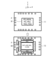
- FIG. 7 is a plan view schematically showing the structure of the solid-state image sensor of the second embodiment.
- FIG. 7 schematically shows the planar configuration of the upper substrate 11, the intermediate substrate 12, and the lower substrate 13.
- Reference numeral P represents a pad electrode.
- Reference numeral B1 is a photodiode PD, a memory unit MEM, a floating diffusion unit FD, a diffusion unit OFD, a first transfer transistor TRZ, a second transfer transistor TRY (not shown), a third transfer transistor TRX, and a third in the upper substrate 11.
- Reference numeral B3 represents a region in which the reset transistor RST, the amplification transistor AMP, the selection transistor SEL, the capacitor C, the FDG, and the like are arranged in the lower substrate 13.
- the logic circuits such as the ADC, the memory / signal processing unit, the V driver, and the I / F of the present embodiment are arranged around the area B3. Further, the pad electrode P of the present embodiment is arranged around the region B1 or around the region B3 and the logic circuit.
- the intermediate substrate 12 by not using the intermediate substrate 12, it is possible to reduce the cost of the substrate for manufacturing the solid-state image sensor.
- the amplification transistor AMP or the like and the logic circuit are formed on different substrates as compared with the case where the amplification transistor AMP or the like and the logic circuit are formed on different substrates. It is possible to simplify the process of forming the logic circuit and the like.
- the logic circuit is arranged around the region B3, the area of the integrated circuit of the solid-state image sensor is larger than that in the case of the first embodiment.
- the structure of the present embodiment is adopted, for example, when it is desired to reduce the cost of the substrate.
- the photodiode PD of the present embodiment is provided in the substrate 21 which is a substrate other than the ⁇ 100 ⁇ substrate, and the amplification transistor AMP of the present embodiment has a crystal plane different from the crystal plane of the substrate 21. It is provided on the substrate 41. Therefore, according to the present embodiment, it is possible to use a substrate other than the ⁇ 100 ⁇ substrate while suppressing the problem of the substrate other than the ⁇ 100 ⁇ substrate (for example, the ⁇ 111 ⁇ substrate).
- FIG. 8 is a cross-sectional view showing the structure of the solid-state image sensor of the third embodiment.
- the solid-state image sensor of this embodiment includes an upper substrate 11, an intermediate substrate 12, and a lower substrate 13.
- the lower substrate 13 of the present embodiment includes only the substrate 41, and functions exclusively as a support substrate that supports the substrate 21 and the substrate 31.
- the logic circuit of this embodiment is provided not on the upper surface of the substrate 41 but on the lower surface of the substrate 31.
- FIG. 9 is a circuit diagram showing the configuration of the solid-state image sensor of the third embodiment.
- FIG. 9 shows various circuit elements provided in the upper substrate 11, the intermediate substrate 12, and the lower substrate 13. Note that in this embodiment, the constant current source is provided in the intermediate substrate 12.
- FIG. 10 is a plan view schematically showing the structure of the solid-state image sensor of the third embodiment.
- FIG. 10 schematically shows the planar configuration of the upper substrate 11, the intermediate substrate 12, and the lower substrate 13.
- Reference numeral P represents a pad electrode.
- Reference numeral C1 indicates that the photodiode PD, the memory unit MEM, the floating diffusion unit FD, the diffusion unit OFD, the first transfer transistor TRZ, the second transfer transistor TRY (not shown), the third transfer transistor TRX, and the third transfer transistor TRX in the upper substrate 11.
- Reference numeral C2 represents a region in which the reset transistor RST, the amplification transistor AMP, the selection transistor SEL, the capacitor C, the FDG, and the like are arranged in the intermediate substrate 12.
- the logic circuits such as the ADC, the memory / signal processing unit, the V driver, and the I / F of the present embodiment are arranged around the area C2. Further, the pad electrode P of the present embodiment is arranged around the region C1 and around the region C2 and the logic circuit.
- the lower substrate 13 exclusively as a support substrate, it is possible to improve the degree of freedom in selecting the type of the substrate 41.
- the amplification transistor AMP or the like and the logic circuit are formed on different substrates as compared with the case where the amplification transistor AMP or the like and the logic circuit are formed on different substrates. It is possible to simplify the process of forming the logic circuit and the like.
- the logic circuit is arranged around the region C2, the area of the integrated circuit of the solid-state image sensor is larger than that in the case of the first embodiment.
- the structure of the present embodiment is adopted, for example, when it is desired to improve the degree of freedom in selecting the type of the substrate 41.
- the photodiode PD of the present embodiment is provided in the substrate 21 which is a substrate other than the ⁇ 100 ⁇ substrate, and the amplification transistor AMP of the present embodiment has a crystal plane different from the crystal plane of the substrate 21. It is provided on the substrate 31. Therefore, according to the present embodiment, it is possible to use a substrate other than the ⁇ 100 ⁇ substrate while suppressing the problem of the substrate other than the ⁇ 100 ⁇ substrate (for example, the ⁇ 111 ⁇ substrate).
- FIG. 11 is a cross-sectional view showing the structure of the solid-state image sensor of the fourth embodiment.
- FIG. 11 shows a vertical cross section of one pixel 1 included in the pixel array region 2 of FIG.
- the solid-state image sensor of this embodiment includes an upper substrate 11, an intermediate substrate 12, and a lower substrate 13.
- the lower substrate 13 of the present embodiment includes only the substrate 41, and functions exclusively as a support substrate that supports the substrate 21 and the substrate 31.
- the logic circuit of this embodiment is provided not on the upper surface of the substrate 41 but on the lower surface of the substrate 31 and the upper surface or the lower surface of the substrate 61 described later.
- FIG. 12 is another cross-sectional view showing the structure of the solid-state image sensor of the fourth embodiment.
- FIG. 12 shows a vertical cross section of the solid-state image sensor of the present embodiment, but shows a vertical cross section different from the vertical cross section shown in FIG.
- FIG. 12 shows the upper substrate 11, the intermediate substrate 12, and the lower substrate 13 in the same manner as in FIG.
- the intermediate substrate 12 includes a transistor TR included in a logic circuit, and has diffusion layers 31d, 31e, and 31f in the substrate 31.
- the diffusion layers 31d and 31e in the substrate 31 function as a drain region and a source region of the transistor TR.
- the insulating film 32 functions as a gate insulating film of the transistor TR, and the gate electrode 43 is included in the transistor TR.
- the solid-state imaging device of the present embodiment further includes a plug 55, a wiring layer 56, a plug 57, a plurality of metal pads 58, a substrate 61 in the loading substrate 17, an insulating film 62, and a plurality of metal pads 63. It includes a plurality of solder balls 71.
- the substrate 61 is an example of the fourth substrate of the present disclosure.
- the loading board 17 of this embodiment is a logic board (logic chip) including a logic circuit.
- the plug 55 is provided on the wiring layer 35b.
- the plug 55 is provided in the substrate 31 via an insulating film ⁇ .
- the wiring layer 56 includes wiring provided on the plug 55 and is arranged in the interlayer insulating film 24.
- the plug 57 is provided on the wiring in the wiring layer 56.
- the plug 57 is provided in the substrate 21 or the like via an insulating film ⁇ .
- the plurality of metal pads 58 include the metal pads 58 provided on the plug 57 and are arranged in the flattening film 14. The upper surface of these metal pads 58 is exposed from the flattening film 14.
- the flattening film 14 is, for example, an insulating film whose upper surface is flattened by CMP.
- the substrate 61 is provided above the substrate 21 via a solder ball 71 or the like.
- the substrate 61 is, for example, a semiconductor substrate such as a silicon substrate.
- the substrate 61 of the present embodiment has a crystal plane different from the crystal plane of the substrate 21.
- the substrate 61 of the present embodiment is a semiconductor substrate other than the ⁇ 111 ⁇ substrate, for example, a ⁇ 100 ⁇ substrate.
- the substrate 61 may be a ⁇ 110 ⁇ substrate.
- the logic circuit may be provided on the upper surface of the substrate 61, or the logic circuit may be provided on the lower surface of the substrate 61.
- the insulating film 62 is provided on the lower surface of the substrate 61.
- the insulating film 62 is, for example, a silicon oxide film.
- the plurality of metal pads 63 are provided in the insulating film 62. The lower surface of these metal pads 63 is exposed from the insulating film 62.
- the solder ball 71 is provided between the metal pad 58 and the metal pad 63.
- the loading substrate 17 is electrically connected to the upper substrate 11 and the intermediate substrate 12 via these metal pads 58 and 63.
- FIG. 13 is a circuit diagram showing the configuration of the solid-state image sensor of the fourth embodiment.
- FIG. 13 shows various circuit elements provided in the upper substrate 11, the intermediate substrate 12, the lower substrate 13, and the loading substrate 17. It should be noted that in this embodiment, the constant current source is provided in the loading substrate 17.
- FIG. 14 is a plan view schematically showing the structure of the solid-state image sensor of the fourth embodiment.
- FIG. 14 schematically shows the planar configuration of the upper substrate 11, the intermediate substrate 12, and the lower substrate 13.
- Reference numeral P represents a pad electrode.
- Reference numeral D1 is a photodiode PD, a memory unit MEM, a floating diffusion unit FD, a diffusion unit OFD, a first transfer transistor TRZ, a second transfer transistor TRY (not shown), a third transfer transistor TRX, and a third transfer transistor TRX in the upper substrate 11.
- Reference numeral D2 represents a region in which the reset transistor RST, the amplification transistor AMP, the selection transistor SEL, the capacitor C, the FDG, and the like are arranged in the intermediate substrate 12.
- the V driver of this embodiment is arranged around the area D2.
- other logic circuits such as the ADC, the memory / signal processing unit, the V driver, and the I / F of the present embodiment are arranged in the loading board 17 provided above the area around the area D1.
- the pad electrodes P of the present embodiment are arranged around the region D1 and around the regions D2 and the V driver.
- the lower substrate 13 exclusively as a support substrate, it is possible to improve the degree of freedom in selecting the type of the substrate 41.
- the present embodiment by arranging many parts of the logic circuit in the loading substrate 17, the area of the integrated circuit of the solid-state image sensor is reduced as compared with the case of the second and third embodiments. It becomes possible.
- the structure of the present embodiment is adopted, for example, when it is desired to reduce the area of the integrated circuit of the solid-state image pickup device while increasing the degree of freedom in selecting the type of the substrate 41.
- the reset transistor RST, amplification transistor AMP, and selection transistor SEL of this embodiment may be arranged in the loading substrate 17.
- the photodiode PD of the present embodiment is provided in the substrate 21 which is a substrate other than the ⁇ 100 ⁇ substrate, and the amplification transistor AMP of the present embodiment has a crystal plane different from the crystal plane of the substrate 21. It is provided on the substrate 31. Therefore, according to the present embodiment, it is possible to use a substrate other than the ⁇ 100 ⁇ substrate while suppressing the problem of the substrate other than the ⁇ 100 ⁇ substrate (for example, the ⁇ 111 ⁇ substrate).
- FIG. 15 is a block diagram showing a configuration example of an electronic device.
- the electrical device shown in FIG. 15 is a camera 100.
- the camera 100 includes an optical unit 101 including a lens group and the like, an image pickup device 102 which is a solid-state image pickup device according to any one of the first to fourth embodiments, and a DSP (Digital Signal Processor) circuit 103 which is a camera signal processing circuit.
- the DSP circuit 103, the frame memory 104, the display unit 105, the recording unit 106, the operation unit 107, and the power supply unit 108 are connected to each other via the bus line 109.
- the optical unit 101 captures incident light (image light) from the subject and forms an image on the imaging surface of the imaging device 102.
- the image pickup apparatus 102 converts the amount of incident light imaged on the image pickup surface by the optical unit 101 into an electric signal in pixel units and outputs it as a pixel signal.
- the DSP circuit 103 performs signal processing on the pixel signal output by the image pickup device 102.
- the frame memory 104 is a memory for storing one screen of a moving image or a still image captured by the imaging device 102.
- the display unit 105 includes a panel-type display device such as a liquid crystal panel or an organic EL panel, and displays a moving image or a still image captured by the image pickup device 102.
- the recording unit 106 records a moving image or a still image captured by the imaging device 102 on a recording medium such as a hard disk or a semiconductor memory.
- the operation unit 107 issues operation commands for various functions of the camera 100 under the operation of the user.
- the power supply unit 108 appropriately supplies various power sources that serve as operating power sources for the DSP circuit 103, the frame memory 104, the display unit 105, the recording unit 106, and the operation unit 107 to these supply targets.
- the solid-state image sensor can be applied to various other products.
- the solid-state imaging device may be mounted on various moving objects such as automobiles, electric vehicles, hybrid electric vehicles, motorcycles, bicycles, personal mobility, airplanes, drones, ships, and robots.
- FIG. 16 is a block diagram showing a configuration example of a mobile control system.
- the mobile control system shown in FIG. 16 is a vehicle control system 200.
- the vehicle control system 200 includes a plurality of electronic control units connected via the communication network 201.
- the vehicle control system 200 includes a drive system control unit 210, a body system control unit 220, an external information detection unit 230, an in-vehicle information detection unit 240, and an integrated control unit 250.
- FIG. 16 further shows a microprocessor 251, an audio image output unit 252, and an in-vehicle network I / F (Interface) 253 as constituents of the integrated control unit 250.
- the drive system control unit 210 controls the operation of the device related to the drive system of the vehicle according to various programs.
- the drive system control unit 210 includes a driving force generator for generating a driving force of a vehicle such as an internal combustion engine and a driving motor, a driving force transmission mechanism for transmitting the driving force to wheels, and a steering wheel of the vehicle. It functions as a control device such as a steering mechanism that adjusts the angle and a braking device that generates braking force for the vehicle.
- the body system control unit 220 controls the operation of various devices mounted on the vehicle body according to various programs.
- the body system control unit 220 functions as a control device for a smart key system, a keyless entry system, a power window device, various lamps (for example, a head lamp, a back lamp, a brake lamp, a blinker, a fog lamp) and the like.
- the body system control unit 220 may be input with radio waves transmitted from a portable device that substitutes for the key or signals of various switches.
- the body system control unit 220 receives such an input of radio waves or signals and controls a vehicle door lock device, a power window device, a lamp, and the like.
- the vehicle outside information detection unit 230 detects information outside the vehicle equipped with the vehicle control system 200.
- an image pickup unit 231 is connected to the vehicle exterior information detection unit 230.
- the vehicle exterior information detection unit 230 causes the image pickup unit 231 to capture an image of the outside of the vehicle, and receives the captured image from the image pickup unit 231.
- the vehicle exterior information detection unit 230 may perform object detection processing or distance detection processing such as a person, a vehicle, an obstacle, a sign, or a character on a road surface based on the received image.
- the imaging unit 231 is an optical sensor that receives light and outputs an electric signal according to the amount of the light received.
- the image pickup unit 231 can output an electric signal as an image or can output it as distance measurement information.
- the light received by the imaging unit 231 may be visible light or invisible light such as infrared light.
- the image pickup unit 231 includes the solid-state image pickup device according to any one of the first to fourth embodiments.
- the in-vehicle information detection unit 240 detects information inside the vehicle equipped with the vehicle control system 200.
- a driver state detection unit 241 that detects the driver's state is connected to the vehicle interior information detection unit 240.
- the driver state detection unit 241 includes a camera that images the driver, and the in-vehicle information detection unit 240 has a degree of fatigue or concentration of the driver based on the detection information input from the driver state detection unit 241. May be calculated, or it may be determined whether or not the driver is dozing.
- This camera may include the solid-state image sensor according to any one of the first to fourth embodiments, and may be, for example, the camera 100 shown in FIG.
- the microcomputer 251 calculates a control target value of the driving force generator, the steering mechanism, or the braking device based on the information inside and outside the vehicle acquired by the outside information detection unit 230 or the inside information detection unit 240, and controls the drive system.
- a control command can be output to the unit 210.
- the microcomputer 251 is a coordinated control for the purpose of realizing ADAS (Advanced Driver Assistance System) functions such as vehicle collision avoidance, impact mitigation, follow-up running based on inter-vehicle distance, vehicle speed maintenance running, collision warning, and lane deviation warning. It can be performed.
- ADAS Advanced Driver Assistance System
- the microcomputer 251 controls the driving force generator, the steering mechanism, or the braking device based on the information around the vehicle acquired by the vehicle exterior information detection unit 230 or the vehicle interior information detection unit 240, so that the driver can control the driver. It is possible to perform coordinated control for the purpose of automatic driving that runs autonomously without depending on the operation.
- the microcomputer 251 can output a control command to the body system control unit 220 based on the information outside the vehicle acquired by the vehicle exterior information detection unit 230.
- the microcomputer 251 controls the headlamps according to the position of the preceding vehicle or the oncoming vehicle detected by the external information detection unit 230, and performs cooperative control for the purpose of anti-glare such as switching the high beam to the low beam. It can be carried out.
- the audio image output unit 252 transmits an output signal of at least one of audio and image to an output device capable of visually or audibly notifying the passenger of the vehicle or the outside of the vehicle.
- an output device capable of visually or audibly notifying the passenger of the vehicle or the outside of the vehicle.
- an audio speaker 261 and a display unit 262, and an instrument panel 263 are shown.
- the display unit 262 may include, for example, an onboard display or a heads-up display.
- FIG. 17 is a plan view showing a specific example of the set position of the imaging unit 231 of FIG.
- the vehicle 300 shown in FIG. 17 includes imaging units 301, 302, 303, 304, and 305 as the imaging unit 231.
- the imaging units 301, 302, 303, 304, and 305 are provided at positions such as the front nose, side mirrors, rear bumpers, back doors, and the upper part of the windshield in the vehicle interior of the vehicle 300, for example.
- the imaging unit 301 provided in the front nose mainly acquires an image in front of the vehicle 300.
- the image pickup unit 302 provided on the left side mirror and the image pickup section 303 provided on the right side mirror mainly acquire an image of the side of the vehicle 300.
- the imaging unit 304 provided on the rear bumper or the back door mainly acquires an image of the rear of the vehicle 300.
- the imaging unit 305 provided on the upper part of the windshield in the vehicle interior mainly acquires an image in front of the vehicle 300.
- the imaging unit 305 is used, for example, to detect a preceding vehicle, a pedestrian, an obstacle, a traffic light, a traffic sign, a lane, or the like.
- FIG. 17 shows an example of the imaging range of the imaging units 301, 302, 303, 304 (hereinafter referred to as “imaging unit 301 to 304”).
- the imaging range 311 indicates the imaging range of the imaging unit 301 provided on the front nose.
- the imaging range 312 indicates the imaging range of the imaging unit 302 provided on the left side mirror.
- the imaging range 313 indicates the imaging range of the imaging unit 303 provided on the right side mirror.
- the imaging range 314 indicates the imaging range of the imaging unit 304 provided on the rear bumper or the back door.
- the imaging range 311, 312, 313, 314 will be referred to as "imaging range 311 to 314".
- At least one of the imaging units 301 to 304 may have a function of acquiring distance information.
- at least one of the imaging units 301 to 304 may be a stereo camera including a plurality of imaging devices, or an imaging device having pixels for detecting a phase difference.
- the microcomputer 251 uses the distance information obtained from the imaging units 301 to 304 to obtain the distance to each three-dimensional object within the imaging range 311 to 314 and the temporal change of this distance (vehicle 300). Relative velocity to) is calculated. Based on these calculation results, the microcomputer 251 is the closest three-dimensional object on the traveling path of the vehicle 300, and is a three-dimensional object traveling at a predetermined speed (for example, 0 km / h or more) in almost the same direction as the vehicle 300. , Can be extracted as a preceding vehicle.
- a predetermined speed for example, 0 km / h or more
- the microcomputer 251 can set an inter-vehicle distance to be secured in front of the preceding vehicle in advance, and can perform automatic braking control (including follow-up stop control), automatic acceleration control (including follow-up start control), and the like. As described above, according to this example, it is possible to perform coordinated control for the purpose of automatic driving or the like in which the vehicle travels autonomously without being operated by the driver.
- the microcomputer 251 classifies three-dimensional object data related to a three-dimensional object into two-wheeled vehicles, ordinary vehicles, large vehicles, pedestrians, utility poles, and other three-dimensional objects based on the distance information obtained from the imaging units 301 to 304. It can be extracted and used for automatic avoidance of obstacles. For example, the microcomputer 251 identifies obstacles around the vehicle 300 into obstacles that can be seen by the driver of the vehicle 300 and obstacles that are difficult to see. Then, the microcomputer 251 determines the collision risk indicating the risk of collision with each obstacle, and when the collision risk is equal to or higher than the set value and there is a possibility of collision, the microcomputer 251 is used via the audio speaker 261 or the display unit 262. By outputting an alarm to the driver and performing forced deceleration and avoidance steering via the drive system control unit 210, driving support for collision avoidance can be provided.
- At least one of the imaging units 301 to 304 may be an infrared camera that detects infrared rays.
- the microcomputer 251 can recognize a pedestrian by determining whether or not a pedestrian is present in the captured images of the imaging units 301 to 304.
- pedestrian recognition is, for example, whether or not the pedestrian is a pedestrian by performing a procedure for extracting feature points in the captured images of the imaging units 301 to 304 as an infrared camera and a pattern matching process on a series of feature points indicating the outline of the object. It is performed by the procedure for determining.
- the audio image output unit 252 When the microcomputer 251 determines that a pedestrian is present in the captured images of the imaging units 301 to 304 and recognizes the pedestrian, the audio image output unit 252 has a square contour line for emphasizing the recognized pedestrian.
- the display unit 262 is controlled so as to superimpose and display. Further, the audio image output unit 252 may control the display unit 262 so as to display an icon or the like indicating a pedestrian at a desired position.
- the first substrate which is a substrate other than the ⁇ 100 ⁇ substrate, and A photoelectric conversion unit provided in the first substrate and A lens provided above the first substrate and One or more substrates provided below the first substrate and having a crystal plane different from the crystal plane of the first substrate.
- a transistor provided on the upper surface or the lower surface of any one of the above-mentioned one or more substrates and included in the source follower circuit, and A solid-state image sensor.
- the first substrate is A vertical trench extending in the vertical direction and Includes a lateral trench extending laterally and connected to the longitudinal trench.
- the first substrate is a ⁇ 111 ⁇ substrate.
- the substrate on which the transistor is provided is a ⁇ 100 ⁇ substrate or a ⁇ 110 ⁇ substrate.
- the one or more substrates include a second substrate provided below the first substrate and with a capacitor on the bottom surface.
- the one or more substrates include a third substrate provided below the first substrate and provided with a capacitor and a logic circuit on the upper surface.
- the one or more substrates include a second substrate provided below the first substrate and provided with a capacitor and a logic circuit on the lower surface.
- the one or more substrates include the second substrate provided below the first substrate and with a capacitor on the bottom surface.
- the solid-state image pickup device according to (16), further comprising a fourth substrate provided above the first substrate and having a logic circuit provided on an upper surface or a lower surface.
- An electronic device equipped with an imaging device The image pickup device
- the first substrate which is a substrate other than the ⁇ 100 ⁇ substrate, and A photoelectric conversion unit provided in the first substrate and A lens provided above the first substrate and One or more substrates provided below the first substrate and having a crystal plane different from the crystal plane of the first substrate.
- a transistor provided on the upper surface or the lower surface of any one of the above-mentioned one or more substrates and included in the source follower circuit, and Equipped with electronic equipment.
Landscapes
- Solid State Image Pick-Up Elements (AREA)
Abstract
[課題]{100}基板以外の基板の問題を抑制しつつ、{100}基板以外の基板を使用することが可能な固体撮像装置および電子機器を提供する。 [解決手段]本開示の固体撮像装置は、{100}基板以外の基板である第1基板と、前記第1基板内に設けられた光電変換部と、前記第1基板の上方に設けられたレンズと、前記第1基板の下方に設けられており、前記第1基板の結晶面と異なる結晶面を有する1つ以上の基板と、前記1つ以上の基板のいずれかの上面または下面に設けられ、ソースフォロワ回路に含まれるトランジスタとを備える。
Description
本開示は、固体撮像装置および電子機器に関する。
固体撮像装置は、{100}基板以外の基板を使用して製造されることがある。例えば、半導体基板内に縦トレンチと横トレンチとを形成する場合には、半導体基板として{111}基板を使用することで、半導体基板内に縦トレンチと横トレンチとをエッチングにより形成しやすくなる。
しかしながら、半導体基板に形成される回路素子の中には、{111}基板など、{100}基板以外の基板に形成されると特性が悪くなるものがあることが問題となる。
そこで、本開示は、{100}基板以外の基板の問題を抑制しつつ、{100}基板以外の基板を使用することが可能な固体撮像装置および電子機器を提供する。
本開示の第1の側面の固体撮像装置は、{100}基板以外の基板である第1基板と、前記第1基板内に設けられた光電変換部と、前記第1基板の上方に設けられたレンズと、前記第1基板の下方に設けられており、前記第1基板の結晶面と異なる結晶面を有する1つ以上の基板と、前記1つ以上の基板のいずれかの上面または下面に設けられ、ソースフォロワ回路に含まれるトランジスタとを備える。これにより例えば、ソースフォロワ回路の特性が悪くなるという{111}基板の問題を抑制しつつ、第1基板として{111}基板を使用することが可能となる。
また、この第1の側面において、前記第1基板は、縦方向に延びる縦トレンチと、横方向に延び、前記縦トレンチに接続されている横トレンチとを含み、前記横トレンチは、前記第1基板内の前記光電変換部と電荷保持部との間に設けられた遮光膜を含んでいてもよい。これにより例えば、縦トレンチと横トレンチとを形成しやすくなるという{111}基板の利点を享受することが可能となる。
また、この第1の側面において、前記遮光膜は、前記横トレンチおよび前記縦トレンチ内に設けられていてもよい。これにより、例えば縦トレンチを介して横トレンチ内に遮光膜を埋め込むことが可能となる。
また、この第1の側面において、前記遮光膜は、前記横トレンチおよび前記縦トレンチ内に素子分離絶縁膜を介して設けられていてもよい。これにより、例えば縦トレンチを介して横トレンチ内に素子分離絶縁膜を埋め込むことが可能となる。
また、この第1の側面において、前記第1基板は、{111}基板でもよく、前記トランジスタが設けられた基板は、{100}基板または{110}基板でもよい。これにより、ソースフォロワ回路のトランジスタを{100}基板または{110}基板に形成することが可能となる。
また、この第1の側面の固体撮像装置はさらに、前記トランジスタと同じ層内に設けられたキャパシタを備えていてもよい。これにより、例えばソースフォロワ回路のトランジスタとキャパシタとを同じ材料で形成することが可能となる。
また、この第1の側面の固体撮像装置はさらに、前記トランジスタと同じ層内に設けられたロジック回路を備えていてもよい。これにより、例えばソースフォロワ回路のトランジスタとロジック回路とを同じ材料で形成することが可能となる。
また、この第1の側面において、前記トランジスタは、前記第1基板内の浮遊拡散部に電気的に接続された増幅トランジスタでもよい。これにより例えば、増幅トランジスタの特性が悪くなるという{111}基板の問題を抑制しつつ、第1基板として{111}基板を使用することが可能となる。
また、この第1の側面において、前記トランジスタは、前記1つ以上の基板のいずれかの上面または下面に順に設けられたゲート絶縁膜およびゲート電極を含んでいてもよい。これにより、例えば増幅トランジスタのゲート絶縁膜およびゲート電極と同じ材料でキャパシタやロジック回路を形成することが可能となる。
また、この第1の側面の固体撮像装置はさらに、前記第1基板の下面に設けられた転送トランジスタを備えていてもよい。これにより例えば、転送トランジスタを{111}基板に形成しつつ、ソースフォロワ回路を{111}基板以外の基板に形成することが可能となる。
また、この第1の側面において、前記1つ以上の基板は、前記第1基板の下方に設けられ、下面にキャパシタが設けられた第2基板を含み、前記トランジスタは、前記第2基板の下面に設けられていてもよい。これにより、ソースフォロワ回路のトランジスタをキャパシタ用の基板に形成することが可能となる。
また、この第1の側面において、前記1つ以上の基板はさらに、前記第2基板の下方に設けられ、上面にロジック回路が設けられた第3基板を含んでいてもよい。これにより、ソースフォロワ回路のトランジスタをロジック回路用以外の基板に形成することが可能となる。
また、この第1の側面において、前記1つ以上の基板は、前記第1基板の下方に設けられ、上面にキャパシタおよびロジック回路が設けられた第3基板を含み、前記トランジスタは、前記第3基板の上面に設けられていてもよい。これにより、ソースフォロワ回路のトランジスタをキャパシタおよびロジック回路用の基板に形成することが可能となる。
また、この第1の側面において、前記1つ以上の基板は、前記第1基板の下方に設けられ、下面にキャパシタおよびロジック回路が設けられた第2基板を含み、前記トランジスタは、前記第2基板の下面に設けられていてもよい。これにより、ソースフォロワ回路のトランジスタをキャパシタおよびロジック回路用の基板に形成することが可能となる。
また、この第1の側面において、前記1つ以上の基板はさらに、前記第2基板の下方に設けられた第3基板を含んでいてもよい。これにより、例えばソースフォロワ回路のトランジスタを支持基板以外の基板に形成することが可能となる。
また、この第1の側面において、前記1つ以上の基板は、前記第1基板の下方に設けられ、下面にキャパシタが設けられた前記第2基板を含み、前記トランジスタは、前記第2基板の下面に設けられていてもよい。これにより、ソースフォロワ回路のトランジスタをキャパシタ用の基板に形成することが可能となる。
また、この第1の側面において、前記1つ以上の基板はさらに、前記第2基板の下方に設けられた第3基板を含んでいてもよい。これにより、例えばソースフォロワ回路のトランジスタを支持基板以外の基板に形成することが可能となる。
また、この第1の側面の固体撮像装置はさらに、前記第1基板の上方に設けられ、上面または下面にロジック回路が設けられた第4基板を備えていてもよい。これにより、例えばロジック回路を支持基板以外の基板に形成することが可能となる。
また、この第1の側面において、前記第4基板は、前記第1基板の上方に半田を介して設けられていてもよい。これにより、例えば第4基板に設けられたロジック回路を、第1基板に設けられた画素に電気的に接続することが可能となる。
本開示の第2の側面の電子機器は、撮像装置を備える電子機器であって、前記撮像装置は、{100}基板以外の基板である第1基板と、前記第1基板内に設けられた光電変換部と、前記第1基板の上方に設けられたレンズと、前記第1基板の下方に設けられており、前記第1基板の結晶面と異なる結晶面を有する1つ以上の基板と、前記1つ以上の基板のいずれかの上面または下面に設けられ、ソースフォロワ回路に含まれるトランジスタとを備える。これにより例えば、ソースフォロワ回路の特性が悪くなるという{111}基板の問題を抑制しつつ、第1基板として{111}基板を使用することが可能となる。
以下、本発明の実施形態を、図面を参照して説明する。
(第1実施形態)
図1は、第1実施形態の固体撮像装置の構成を示すブロック図である。
図1は、第1実施形態の固体撮像装置の構成を示すブロック図である。
図1の固体撮像装置は、CMOS(Complementary Metal Oxide Semiconductor)型の固体撮像装置であり、複数の画素1を有する画素アレイ領域2と、制御回路3と、垂直駆動回路4と、複数のカラム信号処理回路5と、水平駆動回路6と、出力回路7と、複数の垂直信号線8と、水平信号線9とを備えている。
各画素1は、光電変換部として機能するフォトダイオードと、複数の画素トランジスタとを備えている。画素トランジスタの例は、転送トランジスタ、リセットトランジスタ、増幅トランジスタ、選択トランジスタなどのMOSトランジスタである。本実施形態の各画素1は、転送トランジスタとして、TRZ、TRY、TRX、TRG、OFGという5つのMOSトランジスタを備えている。
画素アレイ領域2は、2次元アレイ状に配置された複数の画素1を有している。画素アレイ領域2は、光を受光して光電変換を行い、光電変換により生成された信号電荷を増幅して出力する有効画素領域と、黒レベルの基準になる光学的黒を出力するための黒基準画素領域(図示せず)とを含んでいる。一般に、黒基準画素領域は有効画素領域の外周部に配置されている。
制御回路3は、垂直同期信号、水平同期信号、およびマスタクロックに基づいて、垂直駆動回路4、カラム信号処理回路5、水平駆動回路6等の動作の基準となる種々の信号を生成する。制御回路3により生成される信号は、例えばクロック信号や制御信号であり、垂直駆動回路4、カラム信号処理回路5、水平駆動回路6等に入力される。
垂直駆動回路4は、例えばシフトレジスタを備えており、画素アレイ領域2内の各画素1を行単位で順次垂直方向に選択走査する。垂直駆動回路4はさらに、各画素1が受光量に応じて生成した信号電荷に基づく画素信号を、垂直信号線8を通してカラム信号処理回路5に供給する。
カラム信号処理回路5は、例えば画素アレイ領域2内の画素1の列ごとに配置されており、1行分の画素1から出力された信号の信号処理を、黒基準画素領域からの信号に基づいて列ごとに行う。この信号処理の例は、ノイズ除去や信号増幅である。カラム信号処理回路5の出力段には、水平選択スイッチ(図示せず)が水平信号線9との間に設けられている。
水平駆動回路6は、例えばシフトレジスタを備えており、水平走査パルスを順次出力することでカラム信号処理回路5のそれぞれを順番に選択し、カラム信号処理回路5のそれぞれから画素信号を水平信号線9に出力させる。
出力回路7は、カラム信号処理回路5のそれぞれから水平信号線9を通して順次に供給される信号に対し信号処理を行い、この信号処理が行われた信号を出力する。
図2は、第1実施形態の固体撮像装置の構造を示す断面図である。図2は、図1の画素アレイ領域2に含まれる1つの画素1の縦断面を示している。
図2は、互いに垂直なX軸、Y軸、およびZ軸を示している。X方向およびY方向は横方向(水平方向)に相当し、Z方向は縦方向(垂直方向)に相当する。また、+Z方向は上方向に相当し、-Z方向は下方向に相当する。-Z方向は、厳密に重力方向に一致していてもよいし、厳密には重力方向に一致していなくてもよい。
本実施形態の固体撮像装置は、フォトダイオードPDと、メモリ部MEMと、浮遊拡散部FDと、別の拡散部OFDと、第1転送トランジスタTRZと、不図示の第2転送トランジスタTRYと、第3転送トランジスタTRXと、第4転送トランジスタTRGと、不図示の第5転送トランジスタ(排出トランジスタ)OFGと、不図示のリセットトランジスタRSTと、増幅トランジスタAMPと、不図示の選択トランジスタSELと、ロジック回路に含まれるトランジスタTRと、キャパシタCとを備えている。
本実施形態の固体撮像装置はさらに、上部基板11と、中間基板12と、下部基板13と、平坦化膜14と、カラーフィルタ層15と、オンチップレンズ16とを備えている。
上部基板11は、基板21と、絶縁膜22と、ゲート電極23と、層間絶縁膜24とを備えている。基板21は、N型半導体領域21aと、P+型半導体領域21bと、P型半導体領域21cと、N+型半導体領域21dと、N+型半導体領域21eと、N+型半導体領域21fとを含んでいる。基板21は、本開示の第1基板の例である。本実施形態の上部基板11は、画像センサとして機能するセンサ基板となっている。符号VGは、第1転送トランジスタTRZのゲート電極23に含まれる縦型ゲート電極を示している。
中間基板12は、基板31と、絶縁膜32と、ゲート電極33と、層間絶縁膜34と、多層配線構造35と、上部電極36と、絶縁膜37と、下部電極38とを備えている。基板31は、拡散層31a、31b、31cを含んでいる。基板31は、本開示の第2基板の例である。多層配線構造35は、複数のコンタクトプラグ35aと、配線層35bと、ビアプラグ35cと、金属パッド35dとを含んでいる。本実施形態の中間基板12は、キャパシタCを備えるキャパシタ基板となっている。
下部基板13は、基板41と、絶縁膜42と、ゲート電極43と、層間絶縁膜44と、多層配線構造45とを備えている。基板41は、拡散層41a、41b、41cを含んでいる。基板41は、本開示の第3基板の例である。多層配線構造45は、複数のコンタクトプラグ45aと、配線層45bと、ビアプラグ45cと、金属パッド45dとを含んでいる。本実施形態の下部基板13は、ロジック回路を備えるロジック基板となっている。
本実施形態の固体撮像装置はさらに、トレンチ51と、素子分離絶縁膜52と、遮光膜53と、プラグ54とを備えている。トレンチ51は、縦トレンチ51aと、横トレンチ51bとを含んでいる。
基板21は例えば、シリコン(Si)基板などの半導体基板である。本実施形態の基板21は、{111}基板である。図2において、基板21の上面(+Z方向の面)は、基板21の裏面であり、基板21の下面(-Z方向の面)は、基板21の表面である。本実施形態の固体撮像装置は裏面照射型であるため、基板21の上面が、基板21の光入射面となる。基板21は例えば、半導体基板と、半導体基板の下面に形成された半導体層と、を含む基板としてもよい。{111}基板は、本開示の{100}基板以外の基板の例である。
基板21は、N型半導体領域21aなどの不純物半導体領域を含んでいる。P+型半導体領域21bは、N型半導体領域21a下に設けられている。P型半導体領域21cは、P+型半導体領域21b下に設けられている。N+型半導体領域21dは、P型半導体領域21c内に設けられており、基板21の下面付近に位置している。N+型半導体領域21eとN+型半導体領域21fは、P型半導体領域21c下に設けられており、基板21の下面に露出している。
フォトダイオードPDは、PN接合を形成しているN型半導体領域21aとP+型半導体領域21bとを含み、受光した光を電荷に変換して信号電荷を生成する光電変換部として機能する。フォトダイオードPDは、基板21内に画素1ごとに設けられている。
メモリ部MEMは、N+型半導体領域21dを含み、フォトダイオードPDにより生成された信号電荷を保持する電荷保持部として機能する。信号電荷は、N+型半導体領域21d内に蓄積される。
浮遊拡散部FDは、N+型半導体領域21eを含み、メモリ部MEMから転送された信号電荷を電圧信号に変換して出力する電荷電圧変換部として機能する。一方、拡散部OFDは、N+型半導体領域21fを含んでいる。
本実施形態の固体撮像装置は、グローバルシャッタ(GS)方式を採用しており、フォトダイオードPDと浮遊拡散部FDの他にメモリ部MEMを備えている。よって、フォトダイオードPDからの信号電荷を、メモリ部MEMを介して浮遊拡散部FDに供給することができる。加えて、本実施形態の固体撮像装置は、フォトダイオードPDの横方向ではなく縦方向にメモリ部MEMを配置する積層型構造を採用している。これにより、固体撮像装置の集積回路の面積を低減することができる。
絶縁膜22は、基板21の下面に設けられている。絶縁膜22は、例えば酸化シリコン膜である。絶縁膜22は、第1転送トランジスタTRZ、不図示の第2転送トランジスタTRY、第3転送トランジスタTRX、第4転送トランジスタTRG、不図示の第5転送トランジスタOFGのゲート絶縁膜として機能する。
ゲート電極23は、絶縁膜22の下面に設けられている。ゲート電極23は例えば、シリコン(Si)層などの半導体層や、タングステン(W)層、アルミニウム(Al)層、Cu(銅)層、金属シリサイド層などの金属層である。ゲート電極23は、第1転送トランジスタTRZ、不図示の第2転送トランジスタTRY、第3転送トランジスタTRX、第4転送トランジスタTRG、不図示の第5転送トランジスタOFGに含まれている。第1転送トランジスタTRZのゲート電極23は、基板21のP型半導体領域21c、P+型半導体領域21b、およびN型半導体領域21Aa内に絶縁膜22を介して設けられた縦型ゲート電極VGを含んでいる。
第1転送トランジスタTRZは、フォトダイオードPDからメモリ部MEMに信号電荷を転送する。第2転送トランジスタTRYおよび第3転送トランジスタTRXは、メモリ部MEM内で信号電荷を転送する。第4転送トランジスタTRGは、メモリ部MEMから浮遊拡散部FDに信号電荷を転送する。第5転送トランジスタOFGは、フォトダイオードPDと拡散部OFDとの間に設けられており、フォトダイオードPDを初期化、すなわち、フォトダイオードPDの電位を電源電位(VDD電位)にリセットするために使用される。なお、本実施形態の半導体装置は、第2転送トランジスタTRYおよび第3転送トランジスタTRXのうち、第3転送トランジスタTRXのみを備えていてもよい。半導体装置がTRYおよびTRXを備える方が信号電荷の転送の性能が良いが、半導体装置がTRXのみを備える方が半導体装置の構造がシンプルとなる。
層間絶縁膜24は、基板21の下面に絶縁膜22やゲート電極23などを覆うように形成されている。層間絶縁膜24は例えば、酸化シリコン膜、または酸化シリコン膜を含む積層膜である。
基板31は、基板21の下方に層間絶縁膜24を介して設けられており、層間絶縁膜24の下面に接している。基板31は例えば、シリコン基板などの半導体基板である。本実施形態の基板31は、基板21の結晶面と異なる結晶面を有している。具体的には、本実施形態の基板31は、{111}基板以外の半導体基板であり、例えば{100}基板である。基板31は、{110}基板でもよい。図2において、基板31の上面は基板31の裏面であり、基板31の下面は基板31の表面である。基板31は例えば、半導体基板と、半導体基板の下面に形成された半導体層と、を含む基板としてもよい。
絶縁膜32は、基板31の下面に設けられている。絶縁膜32は、例えば酸化シリコン膜である。絶縁膜32は、不図示のリセットトランジスタRST、増幅トランジスタAMP、不図示の選択トランジスタSELのゲート絶縁膜や、キャパシタCの上部誘電膜として機能する。
ゲート電極33は、絶縁膜32の下面に設けられている。ゲート電極33は例えば、シリコン層などの半導体層や、タングステン層、アルミニウム層、銅層、金属シリサイド層などの金属層である。ゲート電極33は、不図示のリセットトランジスタRST、増幅トランジスタAMP、不図示の選択トランジスタSELに含まれている。
リセットトランジスタRSTは、メモリ部MEMおよび浮遊拡散部FDを初期化、すなわち、メモリ部MEMおよび浮遊拡散部FDの電位を電源電位(VDD電位)にリセットするために使用される。
増幅トランジスタAMPは、浮遊拡散部FDから電圧信号を読み出すソースフォロワ回路の入力部として機能する。基板31内の拡散層31a、31bは、増幅トランジスタAMPのドレイン領域およびソース領域として機能する。増幅トランジスタAMPのゲート電極33は、浮遊拡散部FDと電気的に接続されている。拡散層31bは、下部基板13内のロジック回路と電気的に接続されている。本実施形態の増幅トランジスタAMPは、そのソース領域が選択トランジスタSELを介して垂直信号線8(図1)に電気的に接続されることで、垂直信号線8に電気的に接続された定電流源と共にソースフォロワ回路を構成する。増幅トランジスタAMPは、本開示のソースフォロワ回路に含まれるトランジスタの例である。
選択トランジスタSELは、対応する画素1を選択状態にするために使用される。選択トランジスタSELがオンになると、対応する画素1が選択状態に変化し、増幅トランジスタAMPからの画素信号が垂直信号線8を介してカラム信号処理回路5(図1)により読み出される。
上部電極36、絶縁膜37、および下部電極38は、絶縁膜32の下面に順に設けられている。上部電極36は例えば、シリコン層などの半導体層や、タングステン層、アルミニウム層、銅層、金属シリサイド層などの金属層である。本実施形態のゲート電極33と上部電極36は、同じ電極層内に含まれており、絶縁膜32の表面に当該電極層を形成し当該電極層をエッチングにより加工することで形成される。絶縁膜37は、例えば酸化シリコン膜であり、キャパシタCの下部誘電膜として機能する。下部電極38は例えば、シリコン層などの半導体層や、タングステン層、アルミニウム層、銅層、金属シリサイド層などの金属層である。なお、上部電極36、絶縁膜37、および下部電極38は、図2に示す位置とは異なる位置で基板31の下方に設けられていてもよい。
キャパシタCは、拡散層31c、上部電極36、および下部電極38という3つの電極と、これらの電極に挟まれた絶縁膜32および絶縁膜37という2つの誘電膜とを含んでいる。このように、本実施形態のキャパシタCは、基板31の下面に設けられており、本実施形態の増幅トランジスタAMPも、この基板31の下面に設けられている。本実施形態の増幅トランジスタAMPとキャパシタCは同じ層内に設けられており、具体的には、増幅トランジスタAMPのゲート絶縁膜(絶縁膜32)とゲート電極33がそれぞれ、キャパシタCの上部誘電膜(絶縁膜32)と上部電極36と同じ層内に設けられている。本実施形態のキャパシタCは例えば、対応する画素1の画素内容量として使用される。
層間絶縁膜34は、基板31の下面に絶縁膜32、ゲート電極33、上部電極36、絶縁膜37、下部電極38などを覆うように形成されている。層間絶縁膜34は例えば、酸化シリコン膜、または酸化シリコン膜を含む積層膜である。
多層配線構造35は、層間絶縁膜34内に設けられており、複数のコンタクトプラグ35a、配線層35b、ビアプラグ35c、および金属パッド35dを含んでいる。コンタクトプラグ35aは、拡散層31a、31b、31c、ゲート電極33、上部電極36、下部電極38などの下面に設けられている。配線層35bは、これらのコンタクトプラグ35a下に設けられた複数の配線を含んでいる。ビアプラグ35cは、配線層35b下に設けられている。金属パッド35dは、ビアプラグ35c下に設けられ、下部基板13の金属パッド45dと接合されている。これにより、中間基板12と下部基板13がこれらの金属パッド35d、45dを介して電気的に接続されている。
基板41は、基板31の下方に層間絶縁膜34、44を介して設けられている。基板41は例えば、シリコン基板などの半導体基板である。本実施形態の基板41は、基板21の結晶面と異なる結晶面を有している。具体的には、本実施形態の基板41は、{111}基板以外の半導体基板であり、例えば{100}基板である。基板41は、{110}基板でもよい。図2において、基板41の上面は基板41の表面であり、基板41の下面は基板41の裏面である。基板41は例えば、半導体基板と、半導体基板の下面に形成された半導体層と、を含む基板としてもよい。本実施形態の基板41は、基板21や基板31を支持する支持基板として機能する。
絶縁膜42は、基板41の上面に設けられている。絶縁膜42は、例えば酸化シリコン膜である。絶縁膜42は、ロジック回路に含まれるトランジスタTRのゲート絶縁膜として機能する。
ゲート電極43は、絶縁膜42の上面に設けられている。ゲート電極43は例えば、シリコン層などの半導体層や、タングステン層、アルミニウム層、銅層、金属シリサイド層などの金属層である。ゲート電極43は、ロジック回路に含まれるトランジスタTRに含まれている。
本実施形態の下部基板13は、基板41の上面に設けられたロジック回路を備え、図2に示すトランジスタTRは、このロジック回路を構成している。このロジック回路は例えば、固体撮像装置の種々の動作を制御するよう機能する。基板41内の拡散層41a、41bは、このトランジスタTRのドレイン領域およびソース領域として機能する。
層間絶縁膜44は、基板41の上面に絶縁膜42やゲート電極43などを覆うように形成されており、層間絶縁膜34の下面に接している。層間絶縁膜44は例えば、酸化シリコン膜、または酸化シリコン膜を含む積層膜である。
多層配線構造45は、層間絶縁膜44内に設けられており、複数のコンタクトプラグ45a、配線層45b、ビアプラグ45c、および金属パッド45dを含んでいる。コンタクトプラグ45aは、拡散層41a、41b、41c、ゲート電極43などの上面に設けられている。配線層45bは、これらのコンタクトプラグ45a上に設けられた複数の配線を含んでいる。ビアプラグ45cは、配線層45b上に設けられている。金属パッド45dは、ビアプラグ45c上に設けられ、中間基板12の金属パッド35dと接合されている。これにより、中間基板12と下部基板13がこれらの金属パッド35d、45dを介して電気的に接続されている。
トレンチ51は、基板21内などに設けられ、縦方向(Z方向)に延びる縦トレンチ51aと、基板21内に設けられ、横方向(X方向)に延びる横トレンチ51bとを含んでいる。縦トレンチ51aは、配線層35bの上面から基板21の下面を貫通して縦方向に延びており、横トレンチ51bは、縦トレンチ51aに接続されており、縦トレンチ51aから横方向に延びている。縦トレンチ51aは、YZ平面内を拡がる板状の形状を有している。一方、横トレンチ51bは、XY平面内を拡がる板状の形状を有しており、フォトダイオードPDとメモリ部MEMとの間や、フォトダイオードPDと浮遊拡散部FDとの間に設けられている。
素子分離絶縁膜52は、トレンチ51内に埋め込まれており、トレンチ52の側面、上面、および下面に形成されている。素子分離絶縁膜52は、画素1同士を電気的に分離するための膜として機能する。素子分離絶縁膜13は、例えば酸化シリコン膜である。本実施形態の素子分離絶縁膜52は、縦トレンチ51a内にも横トレンチ41b内にも形成されている。
遮光膜53は、素子分離絶縁膜52と同様にトレンチ51内に埋め込まれており、トレンチ51の側面、上面、および下面に素子分離絶縁膜52を介して形成されている。遮光膜53は、基板21の上面からの光を遮光し、フォトダイオードPDとメモリ部MEMとを光学的に分離するための膜として機能する。遮光膜53は例えば、タングステン層などの金属層や、吸光係数の高いカルコパイライト構造の化合物半導体層である。
プラグ54は、上部基板11および中間基板12内に、浮遊拡散部FDと配線層35b内の配線とを電気的に接続するように設けられている。これにより、浮遊拡散部FDと増幅トランジスタAMPのゲート電極33とが電気的に接続されている。なお、プラグ54は、基板31内に絶縁膜αを介して設けられている。
平坦化膜14は、基板21の上面を覆うように基板21の全面に形成されており、これにより基板21の上面上の面が平坦となっている。平坦化膜14は例えば、樹脂膜などの有機膜である。平坦化膜14は、有機膜以外の絶縁膜でもよく、この絶縁膜の上面は、CMP(Chemical Mechanical Polishing)により平坦化されてもよい。
カラーフィルタ層15は、平坦化膜14上に画素1ごとに形成されている。例えば、赤色(R)、緑色(G)、または青色(B)用のカラーフィルタ層15が、赤色、緑色、または青色の画素1のフォトダイオードPDの上方に配置されている。カラーフィルタ層15は、赤外光用のカラーフィルタ層15として、赤外光の画素1のフォトダイオードPDの上方に配置されていてもよい。カラーフィルタ層15は、所定の波長の光が透過できる性質を有しており、カラーフィルタ層15を透過した光が、平坦化膜14を介してフォトダイオードPDに入射する。
オンチップレンズ16は、カラーフィルタ層15上に画素1ごとに形成されている。オンチップレンズ16は、入射した光を集光する性質を有しており、オンチップレンズ16により集光された光は、カラーフィルタ層15および平坦化膜14を介してフォトダイオードPDに入射する。
以上のように、本実施形態の基板21は、{100}基板ではなく{111}基板となっている。この場合、固体撮像装置の回路素子の中には、{111}基板に形成されると特性が悪くなるものがあることが問題となる。このような回路素子の例は、ソースフォロワ回路に含まれる増幅トランジスタAMPである。そこで、本実施形態では、このような回路素子を、{111}基板である基板21ではなく、{100}基板である基板31に形成している。よって、本実施形態によれば、このような回路素子の特性が悪くなるという{111}基板の問題を抑制しつつ、{111}基板を使用することが可能となる。以下、この具体例について詳細に説明する。
上述のように、本実施形態の固体撮像装置は、グローバルシャッタ(GS)方式を採用しており、フォトダイオードPDと浮遊拡散部FDの他にメモリ部MEMを備えている。よって、フォトダイオードPDからの信号電荷を、メモリ部MEMを介して浮遊拡散部FDに供給することができる。加えて、本実施形態の固体撮像装置は、フォトダイオードPDの横方向ではなく縦方向にメモリ部MEMを配置する積層型構造を採用している。これにより、固体撮像装置の集積回路の面積を低減することができる。
積層型構造を採用する場合には、フォトダイオードPDとメモリ部MEMとの間に、横方向に延びる遮光膜53を形成して、フォトダイオードPDとメモリ部MEMとを、遮光膜53により光学的に分離することが望ましい。そこで、本実施形態では、基板21内を縦方向に延びる縦トレンチ51aを形成し、縦トレンチ51aから横方向に延びる横トレンチ51bを形成することで、フォトダイオードFDとメモリ部MEMとの間に横トレンチ51bを形成している。さらに、縦トレンチ51aおよび横トレンチ51b内に遮光膜53を埋め込むことで、横トレンチ51b内に遮光膜53を形成している。なお、本実施形態の縦トレンチ51aは、画素1同士を電気的に分離する素子分離部を形成するために形成されるため、本実施形態では、縦トレンチ51aおよび横トレンチ51b内に素子分離絶縁膜52を介して遮光膜53が埋め込まれる。
基板21内に縦トレンチ51aおよび横トレンチ51bを形成する場合には、基板21を{111}基板とすることが望ましい。これにより、基板21内に縦トレンチ51aおよび横トレンチ51bをエッチングにより形成しやすくなる。例えば、基板21が{111}基板である場合には、基板21内の複数の<110>方向と複数の<112>方向がZ方向に垂直になる。一方、基板21内に横トレンチ51bを形成する際には、基板21内の長い距離をX方向にエッチングしていくため、基板21はX方向にエッチングしやすい、すなわち、X方向のエッチングレートが高いことが望ましい。ここで、{111}基板は、<110>方向のエッチングレートが高いことが分かっている。よって、本実施形態によれば、X方向を<110>方向に平行にすることで、基板21内に横トレンチ51bを容易に形成することが可能となる。
しかしながら、{111}基板は、{100}基板や{110}基板に比べて、界面準位が好適でないことが問題となる。そのため、{111}基板である基板21に、ソースフォロワ回路の増幅トランジスタAMPを設けると、このソースフォロワ回路におけるS/N比(信号/ノイズ比)が悪化してしまう。
そのため、本実施形態の増幅トランジスタAMPは、{111}基板である基板21ではなく、{100}基板である基板31に設けられている。これにより、ソースフォロワ回路におけるS/N比の悪化を抑制することができる。このように、本実施形態によれば、ソースフォロワ回路におけるS/N比が悪化するという{111}基板のデメリットを抑制しつつ、縦トレンチ51aおよび横トレンチ51bを形成しやすくなるという{111}基板のメリットを享受することが可能となる。
なお、増幅トランジスタAMPが設けられる基板31は、{111}基板以外の基板であれば、{100}基板以外の基板としてもよい。基板31は例えば、{110}基板としてもよい。ただし、基板31を{100}基板とすることには、基板31のコストを抑制できるという利点がある。また、増幅トランジスタAMPは、基板31の代わりに基板41に設けてもよい。この場合、基板41は、{111}基板以外の基板であれば、{100}基板以外の基板としてもよい。これは、基板31の場合と同様である。
以下、上述のSi{111}基板や<110>方向等について補足する。
本開示におけるSi{111}基板とは、シリコン単結晶からなり、ミラー指数の表記において{111}で表される結晶面を有する基板またはウェハである。本開示におけるSi{111}基板は、結晶方位が数度ずれた、例えば{111}面から最近接の[110]方向へ数度ずれた基板またはウェハも含む。さらに、これらの基板またはウェハ上の一部または全面にエピタキシャル法等によりシリコン単結晶を成長させたものをも含む。
また、本開示の表記において{111}面は、対称性において互いに等価な結晶面である(111)面、(-111)面、(1-11)面、(11-1)面、(-1-11)面、(-11-1)面、(1-1-1)面および(-1-1-1)面の総称である。したがって、本開示の明細書等におけるSi{111}基板という記載を、例えばSi(1-11)基板と読み替えてもよい。ここで、ミラー指数の負方向の指数を表記するためのバー符号はマイナス符号で代用している。
また、本開示の記載における<110>方向は、対称性において互いに等価な結晶面方向である[110]方向、[101]方向、[011]方向、[-110]方向、[1-10]方向、[-101]方向、[10-1]方向、[0-11]方向、[01-1]方向、[-1-10]方向、[-10-1]方向および[0-1-1]方向の総称であり、いずれかに読み替えてもよい。但し、本開示は、素子形成面と直交する方向と、この素子形成面に直交する方向に対してさらに直交する方向(すなわち素子形成面と平行な方向)とにエッチングを行うものである。
図18は、本開示におけるSi{111}基板の結晶面である{111}面において<110>方向へのエッチングが成立することとなる面と方位との具体的な組み合わせを示したものである。
図18に示したように、{111}面と<110>方向との組み合わせは、96(=8×12)通り存在する。しかしながら、本開示の<110>方向は、素子形成面である{111}面と直交する方向と、素子形成面と平行な方向とに限られる。すなわち、本開示のSi{111}基板における素子形成面と、そのSi{111}基板に対してエッチングを行う方位との組み合わせは、図18において○で示した組合せのいずれかから選択される。
また、本実施形態では、Si{111}基板を用いて、X軸方向へのエッチングが進行する一方、Y軸方向およびZ軸方向には進行しない場合を例示した。しかしながら、本開示はこれに限定されず、X軸方向およびY軸方向の双方、または、X軸方向もしくはY軸方向のいずれか一方にエッチング進行方位があればよい。
Si基板に対して、エッチング溶液を用いた結晶異方性エッチングを行う際、例えばアルカリ溶液を用いたエッチングを行うと、アルカリ溶液によるSiエッチング反応では、Siの結合手とOHイオンの反応により進行するため、表面側に露出する未結合手が多いほどエッチングが進行しやすく、バルク側に伸びるバックボンドが多いほどエッチングが進行しにくいことが知られている。
すなわち、水平遮光部分は基板表面と略水平方向には、Siバックボンドを1または2本、少なくとも3本より少ない数を有するの対して、基板表面と略垂直方向にはSiバックボンドを3本有する。バックボンドとは、例えば図19を例に挙げて説明すると、Si{111}面の法線に対して、Si未結合手側を正方向とすると、反対側の負方向に伸びる結合手を表す。
図19は、{111}面に対して、-19.47°~+19.47°で、バックボンド3本の例を示している。具体的に、光電変換部、水平遮光部分、電荷保持部をSi{111}基板に設ける場合、水平遮光部分は、第1の方向と直交すると共に面指数{111}で表されるSi{111}基板の第1の結晶面に沿った第1の面と、第1の方向に対して傾斜すると共に面指数{111}で表されるSi{111}基板の第2の結晶面に沿った第2の面とを含む。
Si{111}基板には、例えば、図20に示したように、基板表面が<112>方向に対してオフ角があるように加工された基板の場合も含まれる。オフ角が19.47°以下の場合、オフ角を有する基板の場合においても、<111>方向、すなわちSiバックボンドを3本有する方向のエッチングレートに対して、<110>方向、すなわちSiバックボンドを1本有する方向のエッチングレートが十分に高くなる関係性は保たれる。オフ角が大きくなるとステップ数が多くなり、ミクロな段差の密度が高くなるので、好ましくは5°以下がよい。なお、図20の例では基板表面が<112>方向にオフ角がある場合を挙げたが、<110>方向にオフ角がある場合でも構わなく、オフ角の方向は問わない。また、Si面方位は、X線回折法、電子線回折法、電子線後方散乱回折法などを用いて解析可能である。Siバックボンド数は、Siの結品構造で決定されているものであるため、Si面方位を解析することによって、バックボンド数も解析可能である。
図3は、第1実施形態の固体撮像装置の構成を示す回路図である。
図3は、上部基板11、中間基板12、および下部基板13内に設けられた種々の回路素子を示している。上部基板11は、フォトダイオードPDと、メモリ部MEMと、浮遊拡散部FDと、拡散部OFDと、第1転送トランジスタTRZと、第2転送トランジスタTRYと、第3転送トランジスタTRXと、第4転送トランジスタTRGと、第5転送トランジスタOFGとを備えている。中間基板12は、リセットトランジスタRSTと、増幅トランジスタAMPと、選択トランジスタSELと、キャパシタCとを備えている。下部基板13は、図3に示すように定電流源を備えている。
第4転送トランジスタTRG、第3転送トランジスタTRX、および第2転送トランジスタTRYは、浮遊拡散部FDとキャパシタCとの間に直列に配置されており、メモリ部MEMの付近に設けられている。第1転送トランジスタTRZの一方の主端子は、フォトダイオードPDのカソードに接続されており、第1転送トランジスタTRZの他方の主端子は、メモリ部MEMや第3転送トランジスタTRXの付近に設けられている。第5転送トランジスタOFGの一方の主端子は、拡散部OFDに接続されており、第5転送トランジスタOFGの他方の主端子は、メモリ部MEMや第3転送トランジスタTRXの付近に設けられている。
リセットトランジスタRSTは、浮遊拡散部FDに接続されたソース端子と、電源配線(VDD配線)に接続されたドレイン端子とを備えている。増幅トランジスタAMPは、浮遊拡散部FDのソース端子や浮遊拡散部FDに接続されたゲート端子と、電源配線(VDD配線)に接続されたドレイン端子と、選択トランジスタSELに接続されたソース端子とを備えている。増幅トランジスタAMPと選択トランジスタSELは、電源配線(VDD配線)と定電流源との間に直列に配置されている。増幅トランジスタAMPは、そのソース端子が選択トランジスタSELを介して垂直信号線8(図1)に電気的に接続されることで、垂直信号線8に電気的に接続されたこの定電流源と共にソースフォロワ回路を構成する。
図4は、第1実施形態の固体撮像装置の構造を模式的に示す平面図である。
図4は、上部基板11、中間基板12、および下部基板13の平面構成を模式的に示している。符号Pは、パッド電極を表す。符号A1は、上部基板11内において、フォトダイオードPD、メモリ部MEM、浮遊拡散部FD、拡散部OFD、第1転送トランジスタTRZ、第2転送トランジスタTRY(不図示)、第3転送トランジスタTRX、第4転送トランジスタTRG、第5転送トランジスタOFG(不図示)などが配置された領域を表す。符号A2は、中間基板12内において、リセットトランジスタRST、増幅トランジスタAMP、選択トランジスタSEL、キャパシタC、FDG(変換ゲイン切替部)などが配置された領域を表す。符号A3は、下部基板13内において、ADC(アナログデジタル変換部)、メモリ・信号処理部、Vドライバ、I/F(インターフェイス)などのロジック回路が配置された領域を表す。本実施形態のパッド電極Pは、領域A1の周囲や、領域A2の周囲や、領域A3の周囲に配置されている。
本実施形態の増幅トランジスタAMPは、上部基板11の領域A1ではなく、中間基板12の領域A2に配置されている。これにより、増幅トランジスタAMPを{111}基板以外の基板に設けることが可能となり、ソースフォロワ回路におけるS/N比の悪化を抑制することが可能となる。さらには、増幅トランジスタAMPを領域A2に配置することで、領域A1の面積を縮小することが可能となる。
また、本実施形態の増幅トランジスタAMPは、下部基板13の領域A3ではなく、中間基板12の領域A2に配置されている。これにより、増幅トランジスタAMPに起因して領域A3の面積が拡大することを抑制することが可能となる。
このように、本実施形態の増幅トランジスタAMPは、中間基板12の領域A2に配置されている。領域A2の面積を領域A1の面積や領域A3の面積と同程度にする場合、領域A2には、増幅トランジスタAMP以外の回路素子も配置可能となる。よって、本実施形態では、領域A2にリセットトランジスタRST、選択トランジスタSEL、キャパシタC、FDGを配置している。本実施形態によれば、画素内容量であるキャパシタCを領域A2に配置することで、飽和電荷量を増加させることが可能となる。
本実施形態によれば、増幅トランジスタAMPを領域A2に配置することで、領域A1の面積や領域A3の面積を小さくすることが可能となる。そして、領域A2の面積を領域A1の面積や領域A3の面積と同程度とすることで、本実施形態の固体撮像装置の集積回路の面積を低減することが可能となる。
以上のように、本実施形態のフォトダイオードPDは、{100}基板以外の基板である基板21内に設けられ、本実施形態の増幅トランジスタAMPは、基板21の結晶面と異なる結晶面を有する基板31に設けられている。よって、本実施形態によれば、{100}基板以外の基板(例えば{111}基板)の問題を抑制しつつ、{100}基板以外の基板を使用することが可能となる。
以下、第2、第3、および第4実施形態の固体撮像装置について説明する。以下の説明では、これらの実施形態と第1実施形態との相違点を中心に説明し、これらの実施形態と第1実施形態との共通点については説明を省略する。
(第2実施形態)
図5は、第2実施形態の固体撮像装置の構造を示す断面図である。
図5は、第2実施形態の固体撮像装置の構造を示す断面図である。
本実施形態の固体撮像装置は、上部基板11および下部基板13を備えているが、中間基板12を備えていない。
上部基板11は、図2に示す構成要素に加えて、多層配線構造25を備えている。多層配線構造25は、層間絶縁膜24内に設けられており、コンタクトプラグ25aと、配線層25bと、ビアプラグ25cと、金属パッド25dとを備えている。コンタクトプラグ25aは、浮遊拡散部FDの下面に設けられている。配線層25bは、コンタクトプラグ25a下に設けられた配線など、複数の配線を含んでいる。ビアプラグ25cは、配線層25b下に設けられている。金属パッド25dは、ビアプラグ25c下に設けられ、下部基板13の金属パッド45dと接合されている。これにより、上部基板11と下部基板13がこれらの金属パッド25d、45dを介して電気的に接続されている。縦トレンチ51aは、配線層25bの上面から基板21の下面を貫通して縦方向に延びている。
下部基板13は、図2に示す構成要素に加えて、不図示のリセットトランジスタRSTと、増幅トランジスタAMPと、不図示の選択トランジスタSELと、キャパシタCとを備えている。本実施形態の下部基板13は、第1実施形態の下部基板13と同様に、ロジック回路に含まれるトランジスタTRを備えているが、その図示が省略されている。
下部基板13は、上述の基板41、絶縁膜42、ゲート電極43、層間絶縁膜44、および多層配線構造45を備え、さらには下部電極46と、絶縁膜47と、上部電極48とを備えている。基板41は、上述の拡散層41a、41b、41c(不図示)を含み、さらには拡散層41d、41e、41fを含んでいる。多層配線構造45は、上述のコンタクトプラグ45a、配線層45b、ビアプラグ45c、および金属パッド45dを含んでいる。
基板41は、基板21の下方に層間絶縁膜24、44を介して設けられている。本実施形態の基板41は、基板21を支持する支持基板として機能する。
絶縁膜42は、基板41の上面に設けられている。絶縁膜42は、不図示のリセットトランジスタRST、増幅トランジスタAMP、不図示の選択トランジスタSEL、不図示のトランジスタTRのゲート絶縁膜や、キャパシタCの下部誘電膜として機能する。
ゲート電極43は、絶縁膜42の上面に設けられている。ゲート電極43は、不図示のリセットトランジスタRST、増幅トランジスタAMP、不図示の選択トランジスタSEL、不図示のトランジスタTRに含まれている。
基板41内の拡散層41d、41eは、増幅トランジスタAMPのドレイン領域およびソース領域として機能する。増幅トランジスタAMPのゲート電極43は、浮遊拡散部FDと電気的に接続されている。
下部電極46、絶縁膜47、および上部電極48は、絶縁膜42の上面に順に設けられている。下部電極46は例えば、シリコン層などの半導体層や、タングステン層、アルミニウム層、銅層、金属シリサイド層などの金属層である。本実施形態のゲート電極43と下部電極46は、同じ電極層内に含まれており、絶縁膜42の表面に当該電極層を形成し当該電極層をエッチングにより加工することで形成される。絶縁膜47は、例えば酸化シリコン膜であり、キャパシタCの上部誘電膜として機能する。上部電極48は例えば、シリコン層などの半導体層や、タングステン層、アルミニウム層、銅層、金属シリサイド層などの金属層である。
キャパシタCは、拡散層41f、下部電極46、および上部電極48という3つの電極と、これらの電極に挟まれた絶縁膜42および絶縁膜47という2つの誘電膜とを含んでいる。このように、本実施形態のキャパシタCは、基板41の上面に設けられており、本実施形態の増幅トランジスタAMPも、この基板41の上面に設けられている。本実施形態の増幅トランジスタAMPとキャパシタCは同じ層内に設けられており、具体的には、増幅トランジスタAMPのゲート絶縁膜(絶縁膜42)とゲート電極43がそれぞれ、キャパシタCの下部誘電膜(絶縁膜42)と下部電極46と同じ層内に設けられている。本実施形態のキャパシタCは例えば、対応する画素1の画素内容量として使用される。
層間絶縁膜44は、基板41の上面に絶縁膜42、ゲート電極43、下部電極46、絶縁膜47、上部電極48などを覆うように形成されている。
多層配線構造45は、層間絶縁膜44内に設けられており、上述のコンタクトプラグ45a、配線層45b、ビアプラグ45c、および金属パッド45dを含んでいる。コンタクトプラグ45aは、拡散層41a、41b、41c、41d、41e、41f、ゲート電極43、下部電極46、上部電極48などの上面に設けられている。配線層45bは、これらのコンタクトプラグ45a上に設けられた複数の配線を含んでいる。ビアプラグ45cは、配線層45b上に設けられている。金属パッド45dは、ビアプラグ45c上に設けられており、上部基板11の金属パッド25dと接合されている。これにより、上部基板11と下部基板13がこれらの金属パッド25d、45dを介して電気的に接続されている。本実施形態の浮遊拡散部FDと増幅トランジスタAMPのゲート電極43は、金属パッド25d、45dを介して電気的に接続されている。
図6は、第2実施形態の固体撮像装置の構成を示す回路図である。
図6は、上部基板11、中間基板12、および下部基板13内に設けられた種々の回路素子を示している。本実施形態では、リセットトランジスタRSTと、増幅トランジスタAMPと、選択トランジスタSELと、キャパシタCが、下部基板13内に設けられていることに留意されたい。
図7は、第2実施形態の固体撮像装置の構造を模式的に示す平面図である。
図7は、上部基板11、中間基板12、および下部基板13の平面構成を模式的に示している。符号Pは、パッド電極を表す。符号B1は、上部基板11内において、フォトダイオードPD、メモリ部MEM、浮遊拡散部FD、拡散部OFD、第1転送トランジスタTRZ、第2転送トランジスタTRY(不図示)、第3転送トランジスタTRX、第4転送トランジスタTRG、第5転送トランジスタOFG(不図示)などが配置された領域を表す。符号B3は、下部基板13内において、リセットトランジスタRST、増幅トランジスタAMP、選択トランジスタSEL、キャパシタC、FDGなどが配置された領域を表す。本実施形態のADC、メモリ・信号処理部、Vドライバ、I/Fなどのロジック回路は、領域B3の周囲に配置されている。また、本実施形態のパッド電極Pは、領域B1の周囲や、領域B3およびロジック回路の周囲に配置されている。
本実施形態によれば、中間基板12を使用しないことで、固体撮像装置を製造するための基板のコストを低減することが可能となる。また、本実施形態によれば、増幅トランジスタAMP等とロジック回路とを同じ基板41に形成することで、増幅トランジスタAMP等とロジック回路とを別の基板に形成する場合に比べて、増幅トランジスタAMP等とロジック回路とを形成する工程を簡略化することが可能となる。一方、本実施形態では、領域B3の周囲にロジック回路が配置されることから、固体撮像装置の集積回路の面積が第1実施形態の場合に比べて広くなる。本実施形態の構造は例えば、基板のコストを低減したい場合に採用される。
以上のように、本実施形態のフォトダイオードPDは、{100}基板以外の基板である基板21内に設けられ、本実施形態の増幅トランジスタAMPは、基板21の結晶面と異なる結晶面を有する基板41に設けられている。よって、本実施形態によれば、{100}基板以外の基板(例えば{111}基板)の問題を抑制しつつ、{100}基板以外の基板を使用することが可能となる。
(第3実施形態)
図8は、第3実施形態の固体撮像装置の構造を示す断面図である。
図8は、第3実施形態の固体撮像装置の構造を示す断面図である。
本実施形態の固体撮像装置は、上部基板11と、中間基板12と、下部基板13とを備えている。ただし、本実施形態の下部基板13は、基板41のみを備えており、もっぱら基板21や基板31を支持する支持基板として機能する。本実施形態のロジック回路は、基板41の上面ではなく、基板31の下面に設けられている。
図9は、第3実施形態の固体撮像装置の構成を示す回路図である。
図9は、上部基板11、中間基板12、および下部基板13内に設けられた種々の回路素子を示している。本実施形態では、定電流源が中間基板12内に設けられていることに留意されたい。
図10は、第3実施形態の固体撮像装置の構造を模式的に示す平面図である。
図10は、上部基板11、中間基板12、および下部基板13の平面構成を模式的に示している。符号Pは、パッド電極を表す。符号C1は、上部基板11内において、フォトダイオードPD、メモリ部MEM、浮遊拡散部FD、拡散部OFD、第1転送トランジスタTRZ、第2転送トランジスタTRY(不図示)、第3転送トランジスタTRX、第4転送トランジスタTRG、第5転送トランジスタOFG(不図示)などが配置された領域を表す。符号C2は、中間基板12内において、リセットトランジスタRST、増幅トランジスタAMP、選択トランジスタSEL、キャパシタC、FDGなどが配置された領域を表す。本実施形態のADC、メモリ・信号処理部、Vドライバ、I/Fなどのロジック回路は、領域C2の周囲に配置されている。また、本実施形態のパッド電極Pは、領域C1の周囲や、領域C2およびロジック回路の周囲に配置されている。
本実施形態によれば、下部基板13をもっぱら支持基板として使用することで、基板41の種類を選択する自由度を向上させることが可能となる。また、本実施形態によれば、増幅トランジスタAMP等とロジック回路とを同じ基板31に形成することで、増幅トランジスタAMP等とロジック回路とを別の基板に形成する場合に比べて、増幅トランジスタAMP等とロジック回路とを形成する工程を簡略化することが可能となる。一方、本実施形態では、領域C2の周囲にロジック回路が配置されることから、固体撮像装置の集積回路の面積が第1実施形態の場合に比べて広くなる。本実施形態の構造は例えば、基板41の種類を選択する自由度を向上させたい場合に採用される。
以上のように、本実施形態のフォトダイオードPDは、{100}基板以外の基板である基板21内に設けられ、本実施形態の増幅トランジスタAMPは、基板21の結晶面と異なる結晶面を有する基板31に設けられている。よって、本実施形態によれば、{100}基板以外の基板(例えば{111}基板)の問題を抑制しつつ、{100}基板以外の基板を使用することが可能となる。
(第4実施形態)
図11は、第4実施形態の固体撮像装置の構造を示す断面図である。図11は、図1の画素アレイ領域2に含まれる1つの画素1の縦断面を示している。
図11は、第4実施形態の固体撮像装置の構造を示す断面図である。図11は、図1の画素アレイ領域2に含まれる1つの画素1の縦断面を示している。
本実施形態の固体撮像装置は、上部基板11と、中間基板12と、下部基板13とを備えている。ただし、本実施形態の下部基板13は、基板41のみを備えており、もっぱら基板21や基板31を支持する支持基板として機能する。本実施形態のロジック回路は、基板41の上面ではなく、基板31の下面や後述する基板61の上面または下面に設けられている。
図12は、第4実施形態の固体撮像装置の構造を示す別の断面図である。図12は、本実施形態の固体撮像装置の縦断面を示しているが、図11に示す縦断面とは異なる縦断面を示している。
図12は、図11と同様に、上部基板11と、中間基板12と、下部基板13とを示している。中間基板12は、ロジック回路に含まれるトランジスタTRを備え、基板31内に拡散層31d、31e、31fを備えている。基板31内の拡散層31d、31eは、トランジスタTRのドレイン領域およびソース領域として機能する。絶縁膜32は、トランジスタTRのゲート絶縁膜として機能し、ゲート電極43は、トランジスタTRに含まれている。
本実施形態の固体撮像装置はさらに、プラグ55と、配線層56と、プラグ57と、複数の金属パッド58と、積載基板17内の基板61、絶縁膜62、および複数の金属パッド63と、複数の半田ボール71とを備えている。基板61は、本開示の第4基板の例である。本実施形態の積載基板17は、ロジック回路を備えるロジック基板(ロジックチップ)となっている。
プラグ55は、配線層35b上に設けられている。プラグ55は、基板31内に絶縁膜βを介して設けられている。配線層56は、プラグ55上に設けられた配線を含み、層間絶縁膜24内に配置されている。プラグ57は、配線層56内の当該配線上に設けられている。プラグ57は、基板21内などに絶縁膜γを介して設けられている。複数の金属パッド58は、プラグ57上に設けられた金属パッド58を含み、平坦化膜14内に配置されている。これらの金属パッド58の上面は平坦化膜14から露出している。平坦化膜14は例えば、その上面がCMPにより平坦化された絶縁膜である。
基板61は、基板21の上方に半田ボール71等を介して設けられている。基板61は例えば、シリコン基板などの半導体基板である。本実施形態の基板61は、基板21の結晶面と異なる結晶面を有している。具体的には、本実施形態の基板61は、{111}基板以外の半導体基板であり、例えば{100}基板である。基板61は、{110}基板でもよい。本実施形態では、基板61の上面にロジック回路が設けられていてもよいし、基板61の下面にロジック回路が設けられていてもよい。
絶縁膜62は、基板61の下面に設けられている。絶縁膜62は、例えば酸化シリコン膜である。
複数の金属パッド63は、絶縁膜62内に設けられている。これらの金属パッド63の下面は絶縁膜62から露出している。
半田ボール71は、金属パッド58と金属パッド63との間に設けられている。これにより、積載基板17が上部基板11および中間基板12とこれらの金属パッド58、63を介して電気的に接続されている。
図13は、第4実施形態の固体撮像装置の構成を示す回路図である。
図13は、上部基板11、中間基板12、下部基板13、および積載基板17内に設けられた種々の回路素子を示している。本実施形態では、定電流源が積載基板17内に設けられていることに留意されたい。
図14は、第4実施形態の固体撮像装置の構造を模式的に示す平面図である。
図14は、上部基板11、中間基板12、および下部基板13の平面構成を模式的に示している。符号Pは、パッド電極を表す。符号D1は、上部基板11内において、フォトダイオードPD、メモリ部MEM、浮遊拡散部FD、拡散部OFD、第1転送トランジスタTRZ、第2転送トランジスタTRY(不図示)、第3転送トランジスタTRX、第4転送トランジスタTRG、第5転送トランジスタOFG(不図示)などが配置された領域を表す。符号D2は、中間基板12内において、リセットトランジスタRST、増幅トランジスタAMP、選択トランジスタSEL、キャパシタC、FDGなどが配置された領域を表す。本実施形態のVドライバは、領域D2の周囲に配置されている。一方、本実施形態のADC、メモリ・信号処理部、Vドライバ、I/Fなどのその他のロジック回路は、領域D1の周囲の領域の上方に設けられた積載基板17内に配置されている。また、本実施形態のパッド電極Pは、領域D1の周囲や、領域D2およびVドライバの周囲に配置されている。
本実施形態によれば、下部基板13をもっぱら支持基板として使用することで、基板41の種類を選択する自由度を向上させることが可能となる。また、本実施形態によれば、ロジック回路の多くの部分を積載基板17内に配置することで、固体撮像装置の集積回路の面積を、第2および第3実施形態の場合に比べて小さくすることが可能となる。本実施形態の構造は例えば、基板41の種類を選択する自由度を向上させつつ、固体撮像装置の集積回路の面積を縮小したい場合に採用される。なお、本実施形態のリセットトランジスタRST、増幅トランジスタAMP、および選択トランジスタSELは、積載基板17内に配置してもよい。
以上のように、本実施形態のフォトダイオードPDは、{100}基板以外の基板である基板21内に設けられ、本実施形態の増幅トランジスタAMPは、基板21の結晶面と異なる結晶面を有する基板31に設けられている。よって、本実施形態によれば、{100}基板以外の基板(例えば{111}基板)の問題を抑制しつつ、{100}基板以外の基板を使用することが可能となる。
(応用例)
図15は、電子機器の構成例を示すブロック図である。図15に示す電気機器は、カメラ100である。
図15は、電子機器の構成例を示すブロック図である。図15に示す電気機器は、カメラ100である。
カメラ100は、レンズ群などを含む光学部101と、第1から第4実施形態のいずれかの固体撮像装置である撮像装置102と、カメラ信号処理回路であるDSP(Digital Signal Processor)回路103と、フレームメモリ104と、表示部105と、記録部106と、操作部107と、電源部108とを備えている。また、DSP回路103、フレームメモリ104、表示部105、記録部106、操作部107、および電源部108は、バスライン109を介して相互に接続されている。
光学部101は、被写体からの入射光(像光)を取り込んで、撮像装置102の撮像面上に結像する。撮像装置102は、光学部101により撮像面上に結像された入射光の光量を画素単位で電気信号に変換して、画素信号として出力する。
DSP回路103は、撮像装置102により出力された画素信号について信号処理を行う。フレームメモリ104は、撮像装置102で撮像された動画または静止画の1画面を記憶しておくためのメモリである。
表示部105は、例えば液晶パネルや有機ELパネルなどのパネル型表示装置を含んでおり、撮像装置102で撮像された動画または静止画を表示する。記録部106は、撮像装置102で撮像された動画または静止画を、ハードディスクや半導体メモリなどの記録媒体に記録する。
操作部107は、ユーザによる操作の下に、カメラ100が持つ様々な機能について操作指令を発する。電源部108は、DSP回路103、フレームメモリ104、表示部105、記録部106、および操作部107の動作電源となる各種の電源を、これらの供給対象に対して適宜供給する。
撮像装置102として、第1から第4実施形態のいずれかの固体撮像装置を使用することで、良好な画像の取得が期待できる。
当該固体撮像装置は、その他の様々な製品に応用することができる。例えば、当該固体撮像装置は、自動車、電気自動車、ハイブリッド電気自動車、自動二輪車、自転車、パーソナルモビリティ、飛行機、ドローン、船舶、ロボットなどの種々の移動体に搭載されてもよい。
図16は、移動体制御システムの構成例を示すブロック図である。図16に示す移動体制御システムは、車両制御システム200である。
車両制御システム200は、通信ネットワーク201を介して接続された複数の電子制御ユニットを備える。図16に示した例では、車両制御システム200は、駆動系制御ユニット210と、ボディ系制御ユニット220と、車外情報検出ユニット230と、車内情報検出ユニット240と、統合制御ユニット250とを備えている。図16はさらに、統合制御ユニット250の構成部として、マイクロコンピュータ251と、音声画像出力部252と、車載ネットワークI/F(Interface)253とを示している。
駆動系制御ユニット210は、各種プログラムに従って、車両の駆動系に関連する装置の動作を制御する。例えば、駆動系制御ユニット210は、内燃機関や駆動用モータなどの車両の駆動力を発生させるための駆動力発生装置や、駆動力を車輪に伝達するための駆動力伝達機構や、車両の舵角を調節するステアリング機構や、車両の制動力を発生させる制動装置などの制御装置として機能する。
ボディ系制御ユニット220は、各種プログラムに従って、車体に装備された各種装置の動作を制御する。例えば、ボディ系制御ユニット220は、スマートキーシステム、キーレスエントリシステム、パワーウィンドウ装置、各種ランプ(例えば、ヘッドランプ、バックランプ、ブレーキランプ、ウィンカー、フォグランプ)などの制御装置として機能する。この場合、ボディ系制御ユニット220には、鍵を代替する携帯機から発信される電波または各種スイッチの信号が入力され得る。ボディ系制御ユニット220は、このような電波または信号の入力を受け付け、車両のドアロック装置、パワーウィンドウ装置、ランプなどを制御する。
車外情報検出ユニット230は、車両制御システム200を搭載した車両の外部の情報を検出する。車外情報検出ユニット230には、例えば撮像部231が接続される。車外情報検出ユニット230は、撮像部231に車外の画像を撮像させると共に、撮像された画像を撮像部231から受信する。車外情報検出ユニット230は、受信した画像に基づいて、人、車、障害物、標識、路面上の文字などの物体検出処理または距離検出処理を行ってもよい。
撮像部231は、光を受光し、その光の受光量に応じた電気信号を出力する光センサである。撮像部231は、電気信号を画像として出力することもできるし、測距の情報として出力することもできる。撮像部231が受光する光は、可視光であってもよいし、赤外線などの非可視光であってもよい。撮像部231は、第1から第4実施形態のいずれかの固体撮像装置を含んでいる。
車内情報検出ユニット240は、車両制御システム200を搭載した車両の内部の情報を検出する。車内情報検出ユニット240には例えば、運転者の状態を検出する運転者状態検出部241が接続される。例えば、運転者状態検出部241は、運転者を撮像するカメラを含み、車内情報検出ユニット240は、運転者状態検出部241から入力される検出情報に基づいて、運転者の疲労度合いまたは集中度合いを算出してもよいし、運転者が居眠りをしていないかを判別してもよい。このカメラは、第1から第4実施形態のいずれかの固体撮像装置を含んでいてもよく、例えば、図15に示すカメラ100でもよい。
マイクロコンピュータ251は、車外情報検出ユニット230または車内情報検出ユニット240で取得される車内外の情報に基づいて、駆動力発生装置、ステアリング機構、または制動装置の制御目標値を演算し、駆動系制御ユニット210に対して制御指令を出力することができる。例えば、マイクロコンピュータ251は、車両の衝突回避、衝撃緩和、車間距離に基づく追従走行、車速維持走行、衝突警告、レーン逸脱警告などのADAS(Advanced Driver Assistance System)の機能実現を目的とした協調制御を行うことができる。
また、マイクロコンピュータ251は、車外情報検出ユニット230または車内情報検出ユニット240で取得される車両の周囲の情報に基づいて駆動力発生装置、ステアリング機構、または制動装置を制御することにより、運転者の操作によらずに自律的に走行する自動運転などを目的とした協調制御を行うことができる。
また、マイクロコンピュータ251は、車外情報検出ユニット230で取得される車外の情報に基づいて、ボディ系制御ユニット220に対して制御指令を出力することができる。例えば、マイクロコンピュータ251は、車外情報検出ユニット230で検知した先行車または対向車の位置に応じてヘッドランプを制御し、ハイビームをロービームに切り替えるなどの防眩を図ることを目的とした協調制御を行うことができる。
音声画像出力部252は、車両の搭乗者または車外に対して視覚的または聴覚的に情報を通知することが可能な出力装置に、音声および画像のうちの少なくとも一方の出力信号を送信する。図16の例では、このような出力装置として、オーディオスピーカ261、表示部262、およびインストルメントパネル263が示されている。表示部262は例えば、オンボードディスプレイまたはヘッドアップディスプレイを含んでいてもよい。
図17は、図16の撮像部231の設定位置の具体例を示す平面図である。
図17に示す車両300は、撮像部231として、撮像部301、302、303、304、305を備えている。撮像部301、302、303、304、305は例えば、車両300のフロントノーズ、サイドミラー、リアバンパ、バックドア、車室内のフロントガラスの上部などの位置に設けられる。
フロントノーズに備えられる撮像部301は、主として車両300の前方の画像を取得する。左のサイドミラーに備えられる撮像部302と、右のサイドミラーに備えられる撮像部303は、主として車両300の側方の画像を取得する。リアバンパまたはバックドアに備えられる撮像部304は、主として車両300の後方の画像を取得する。車室内のフロントガラスの上部に備えられる撮像部305は、主として車両300の前方の画像を取得する。撮像部305は例えば、先行車両、歩行者、障害物、信号機、交通標識、車線などの検出に用いられる。
図17は、撮像部301、302、303、304(以下「撮像部301~304」と表記する)の撮像範囲の例を示している。撮像範囲311は、フロントノーズに設けられた撮像部301の撮像範囲を示す。撮像範囲312は、左のサイドミラーに設けられた撮像部302の撮像範囲を示す。撮像範囲313は、右のサイドミラーに設けられた撮像部303の撮像範囲を示す。撮像範囲314は、リアバンパまたはバックドアに設けられた撮像部304の撮像範囲を示す。例えば、撮像部301~304で撮像された画像データが重ね合わせられることにより、車両300を上方から見た俯瞰画像が得られる。以下、撮像範囲311、312、313、314を「撮像範囲311~314」と表記する。
撮像部301~304の少なくとも1つは、距離情報を取得する機能を有していてもよい。例えば、撮像部301~304の少なくとも1つは、複数の撮像装置を含むステレオカメラであってもよいし、位相差検出用の画素を有する撮像装置であってもよい。
例えば、マイクロコンピュータ251(図16)は、撮像部301~304から得られた距離情報を基に、撮像範囲311~314内における各立体物までの距離と、この距離の時間的変化(車両300に対する相対速度)を算出する。マイクロコンピュータ251は、これらの算出結果に基づいて、車両300の進行路上にある最も近い立体物で、車両300とほぼ同じ方向に所定の速度(例えば、0km/h以上)で走行する立体物を、先行車として抽出することができる。さらに、マイクロコンピュータ251は、先行車の手前にあらかじめ確保すべき車間距離を設定し、自動ブレーキ制御(追従停止制御も含む)や自動加速制御(追従発進制御も含む)等を行うことができる。このように、この例によれば、運転者の操作によらずに自律的に走行する自動運転等を目的とした協調制御を行うことができる。
例えば、マイクロコンピュータ251は、撮像部301~304から得られた距離情報を基に、立体物に関する立体物データを、2輪車、普通車両、大型車両、歩行者、電柱その他の立体物に分類して抽出し、障害物の自動回避に用いることができる。例えば、マイクロコンピュータ251は、車両300の周辺の障害物を、車両300のドライバが視認可能な障害物と、視認困難な障害物とに識別する。そして、マイクロコンピュータ251は、各障害物との衝突の危険度を示す衝突リスクを判断し、衝突リスクが設定値以上で衝突可能性がある状況であるときには、オーディオスピーカ261や表示部262を介してドライバに警報を出力することや、駆動系制御ユニット210を介して強制減速や回避操舵を行うことで、衝突回避のための運転支援を行うことができる。
撮像部301~304の少なくとも1つは、赤外線を検出する赤外線カメラであってもよい。例えば、マイクロコンピュータ251は、撮像部301~304の撮像画像中に歩行者が存在するか否かを判定することで、歩行者を認識することができる。かかる歩行者の認識は例えば、赤外線カメラとしての撮像部301~304の撮像画像における特徴点を抽出する手順と、物体の輪郭を示す一連の特徴点にパターンマッチング処理を行って歩行者か否かを判別する手順により行われる。マイクロコンピュータ251が、撮像部301~304の撮像画像中に歩行者が存在すると判定し、歩行者を認識すると、音声画像出力部252は、当該認識された歩行者に強調のための方形輪郭線を重畳表示するように、表示部262を制御する。また、音声画像出力部252は、歩行者を示すアイコン等を所望の位置に表示するように表示部262を制御してもよい。
以上、本開示の実施形態について説明したが、これらの実施形態は、本開示の要旨を逸脱しない範囲内で、種々の変更を加えて実施してもよい。例えば、2つ以上の実施形態を組み合わせて実施してもよい。
なお、本開示は、以下のような構成を取ることもできる。
(1)
{100}基板以外の基板である第1基板と、
前記第1基板内に設けられた光電変換部と、
前記第1基板の上方に設けられたレンズと、
前記第1基板の下方に設けられており、前記第1基板の結晶面と異なる結晶面を有する1つ以上の基板と、
前記1つ以上の基板のいずれかの上面または下面に設けられ、ソースフォロワ回路に含まれるトランジスタと、
を備える固体撮像装置。
{100}基板以外の基板である第1基板と、
前記第1基板内に設けられた光電変換部と、
前記第1基板の上方に設けられたレンズと、
前記第1基板の下方に設けられており、前記第1基板の結晶面と異なる結晶面を有する1つ以上の基板と、
前記1つ以上の基板のいずれかの上面または下面に設けられ、ソースフォロワ回路に含まれるトランジスタと、
を備える固体撮像装置。
(2)
前記第1基板は、
縦方向に延びる縦トレンチと、
横方向に延び、前記縦トレンチに接続されている横トレンチとを含み、
前記横トレンチは、前記第1基板内の前記光電変換部と電荷保持部との間に設けられた遮光膜を含む、(1)に記載の固体撮像装置。
前記第1基板は、
縦方向に延びる縦トレンチと、
横方向に延び、前記縦トレンチに接続されている横トレンチとを含み、
前記横トレンチは、前記第1基板内の前記光電変換部と電荷保持部との間に設けられた遮光膜を含む、(1)に記載の固体撮像装置。
(3)
前記遮光膜は、前記横トレンチおよび前記縦トレンチ内に設けられている、(2)に記載の固体撮像装置。
前記遮光膜は、前記横トレンチおよび前記縦トレンチ内に設けられている、(2)に記載の固体撮像装置。
(4)
前記遮光膜は、前記横トレンチおよび前記縦トレンチ内に素子分離絶縁膜を介して設けられている、(3)に記載の固体撮像装置。
前記遮光膜は、前記横トレンチおよび前記縦トレンチ内に素子分離絶縁膜を介して設けられている、(3)に記載の固体撮像装置。
(5)
前記第1基板は、{111}基板であり、
前記トランジスタが設けられた基板は、{100}基板または{110}基板である、
(1)に記載の固体撮像装置。
前記第1基板は、{111}基板であり、
前記トランジスタが設けられた基板は、{100}基板または{110}基板である、
(1)に記載の固体撮像装置。
(6)
さらに、前記トランジスタと同じ層内に設けられたキャパシタを備える、(1)に記載の固体撮像装置。
さらに、前記トランジスタと同じ層内に設けられたキャパシタを備える、(1)に記載の固体撮像装置。
(7)
さらに、前記トランジスタと同じ層内に設けられたロジック回路を備える、(1)に記載の固体撮像装置。
さらに、前記トランジスタと同じ層内に設けられたロジック回路を備える、(1)に記載の固体撮像装置。
(8)
前記トランジスタは、前記第1基板内の浮遊拡散部に電気的に接続された増幅トランジスタである、(1)に記載の固体撮像装置。
前記トランジスタは、前記第1基板内の浮遊拡散部に電気的に接続された増幅トランジスタである、(1)に記載の固体撮像装置。
(9)
前記トランジスタは、前記1つ以上の基板のいずれかの上面または下面に順に設けられたゲート絶縁膜およびゲート電極を含む、(1)に記載の固体撮像装置。
前記トランジスタは、前記1つ以上の基板のいずれかの上面または下面に順に設けられたゲート絶縁膜およびゲート電極を含む、(1)に記載の固体撮像装置。
(10)
さらに、前記第1基板の下面に設けられた転送トランジスタを備える、(1)に記載の固体撮像装置。
さらに、前記第1基板の下面に設けられた転送トランジスタを備える、(1)に記載の固体撮像装置。
(11)
前記1つ以上の基板は、前記第1基板の下方に設けられ、下面にキャパシタが設けられた第2基板を含み、
前記トランジスタは、前記第2基板の下面に設けられている、(1)に記載の固体撮像装置。
前記1つ以上の基板は、前記第1基板の下方に設けられ、下面にキャパシタが設けられた第2基板を含み、
前記トランジスタは、前記第2基板の下面に設けられている、(1)に記載の固体撮像装置。
(12)
前記1つ以上の基板はさらに、前記第2基板の下方に設けられ、上面にロジック回路が設けられた第3基板を含む、(11)に記載の固体撮像装置。
前記1つ以上の基板はさらに、前記第2基板の下方に設けられ、上面にロジック回路が設けられた第3基板を含む、(11)に記載の固体撮像装置。
(13)
前記1つ以上の基板は、前記第1基板の下方に設けられ、上面にキャパシタおよびロジック回路が設けられた第3基板を含み、
前記トランジスタは、前記第3基板の上面に設けられている、(1)に記載の固体撮像装置。
前記1つ以上の基板は、前記第1基板の下方に設けられ、上面にキャパシタおよびロジック回路が設けられた第3基板を含み、
前記トランジスタは、前記第3基板の上面に設けられている、(1)に記載の固体撮像装置。
(14)
前記1つ以上の基板は、前記第1基板の下方に設けられ、下面にキャパシタおよびロジック回路が設けられた第2基板を含み、
前記トランジスタは、前記第2基板の下面に設けられている、(1)に記載の固体撮像装置。
前記1つ以上の基板は、前記第1基板の下方に設けられ、下面にキャパシタおよびロジック回路が設けられた第2基板を含み、
前記トランジスタは、前記第2基板の下面に設けられている、(1)に記載の固体撮像装置。
(15)
前記1つ以上の基板はさらに、前記第2基板の下方に設けられた第3基板を含む、(14)に記載の固体撮像装置。
前記1つ以上の基板はさらに、前記第2基板の下方に設けられた第3基板を含む、(14)に記載の固体撮像装置。
(16)
前記1つ以上の基板は、前記第1基板の下方に設けられ、下面にキャパシタが設けられた前記第2基板を含み、
前記トランジスタは、前記第2基板の下面に設けられている、(1)に記載の固体撮像装置。
前記1つ以上の基板は、前記第1基板の下方に設けられ、下面にキャパシタが設けられた前記第2基板を含み、
前記トランジスタは、前記第2基板の下面に設けられている、(1)に記載の固体撮像装置。
(17)
前記1つ以上の基板はさらに、前記第2基板の下方に設けられた第3基板を含む、(16)に記載の固体撮像装置。
前記1つ以上の基板はさらに、前記第2基板の下方に設けられた第3基板を含む、(16)に記載の固体撮像装置。
(18)
さらに、前記第1基板の上方に設けられ、上面または下面にロジック回路が設けられた第4基板を備える、(16)に記載の固体撮像装置。
さらに、前記第1基板の上方に設けられ、上面または下面にロジック回路が設けられた第4基板を備える、(16)に記載の固体撮像装置。
(19)
前記第4基板は、前記第1基板の上方に半田を介して設けられている、(18)に記載の固体撮像装置。
前記第4基板は、前記第1基板の上方に半田を介して設けられている、(18)に記載の固体撮像装置。
(20)
撮像装置を備える電子機器であって、
前記撮像装置は、
{100}基板以外の基板である第1基板と、
前記第1基板内に設けられた光電変換部と、
前記第1基板の上方に設けられたレンズと、
前記第1基板の下方に設けられており、前記第1基板の結晶面と異なる結晶面を有する1つ以上の基板と、
前記1つ以上の基板のいずれかの上面または下面に設けられ、ソースフォロワ回路に含まれるトランジスタと、
を備える、電子機器。
撮像装置を備える電子機器であって、
前記撮像装置は、
{100}基板以外の基板である第1基板と、
前記第1基板内に設けられた光電変換部と、
前記第1基板の上方に設けられたレンズと、
前記第1基板の下方に設けられており、前記第1基板の結晶面と異なる結晶面を有する1つ以上の基板と、
前記1つ以上の基板のいずれかの上面または下面に設けられ、ソースフォロワ回路に含まれるトランジスタと、
を備える、電子機器。
1:画素、2:画素アレイ領域、3:制御回路、
4:垂直駆動回路、5:カラム信号処理回路、6:水平駆動回路、
7:出力回路、8:垂直信号線、9:水平信号線、
11:上部基板、12:中間基板、13:下部基板、14:平坦化膜、
15:カラーフィルタ層、16:オンチップレンズ、17:積載基板、
21:基板、21a:N型半導体領域、21b:P+型半導体領域、
21c:P型半導体領域、21d:N+型半導体領域、21e:N+型半導体領域、
21f:N+型半導体領域、22:絶縁膜、23:ゲート電極、
24:層間絶縁膜、25:多層配線構造、25a:コンタクトプラグ、
25b:配線層、25c:ビアプラグ、25d:金属パッド、
31:基板、31a、31b、31c、31d、31e、31f:拡散層、
32:絶縁膜、33:ゲート電極、34:層間絶縁膜、35:多層配線構造、
35a:コンタクトプラグ、35b:配線層、35c:ビアプラグ、
35d:金属パッド、36:上部電極、37:絶縁膜、38:下部電極、
41:基板、41a、41b、41c:拡散層、42:絶縁膜、
43:ゲート電極、44:層間絶縁膜、45:多層配線構造、
45a:コンタクトプラグ、45b:配線層、45c:ビアプラグ、
45d:金属パッド、46:下部電極、47:絶縁膜、48:上部電極、
51:トレンチ、51a:縦トレンチ、51b:横トレンチ、
52:素子分離絶縁膜、53:遮光膜、54、55:プラグ、
56:配線層、57:プラグ、58:金属パッド、
61:基板、62:絶縁膜、63:金属パッド、71:半田ボール
4:垂直駆動回路、5:カラム信号処理回路、6:水平駆動回路、
7:出力回路、8:垂直信号線、9:水平信号線、
11:上部基板、12:中間基板、13:下部基板、14:平坦化膜、
15:カラーフィルタ層、16:オンチップレンズ、17:積載基板、
21:基板、21a:N型半導体領域、21b:P+型半導体領域、
21c:P型半導体領域、21d:N+型半導体領域、21e:N+型半導体領域、
21f:N+型半導体領域、22:絶縁膜、23:ゲート電極、
24:層間絶縁膜、25:多層配線構造、25a:コンタクトプラグ、
25b:配線層、25c:ビアプラグ、25d:金属パッド、
31:基板、31a、31b、31c、31d、31e、31f:拡散層、
32:絶縁膜、33:ゲート電極、34:層間絶縁膜、35:多層配線構造、
35a:コンタクトプラグ、35b:配線層、35c:ビアプラグ、
35d:金属パッド、36:上部電極、37:絶縁膜、38:下部電極、
41:基板、41a、41b、41c:拡散層、42:絶縁膜、
43:ゲート電極、44:層間絶縁膜、45:多層配線構造、
45a:コンタクトプラグ、45b:配線層、45c:ビアプラグ、
45d:金属パッド、46:下部電極、47:絶縁膜、48:上部電極、
51:トレンチ、51a:縦トレンチ、51b:横トレンチ、
52:素子分離絶縁膜、53:遮光膜、54、55:プラグ、
56:配線層、57:プラグ、58:金属パッド、
61:基板、62:絶縁膜、63:金属パッド、71:半田ボール
Claims (20)
- {100}基板以外の基板である第1基板と、
前記第1基板内に設けられた光電変換部と、
前記第1基板の上方に設けられたレンズと、
前記第1基板の下方に設けられており、前記第1基板の結晶面と異なる結晶面を有する1つ以上の基板と、
前記1つ以上の基板のいずれかの上面または下面に設けられ、ソースフォロワ回路に含まれるトランジスタと、
を備える固体撮像装置。 - 前記第1基板は、
縦方向に延びる縦トレンチと、
横方向に延び、前記縦トレンチに接続されている横トレンチとを含み、
前記横トレンチは、前記第1基板内の前記光電変換部と電荷保持部との間に設けられた遮光膜を含む、請求項1に記載の固体撮像装置。 - 前記遮光膜は、前記横トレンチおよび前記縦トレンチ内に設けられている、請求項2に記載の固体撮像装置。
- 前記遮光膜は、前記横トレンチおよび前記縦トレンチ内に素子分離絶縁膜を介して設けられている、請求項3に記載の固体撮像装置。
- 前記第1基板は、{111}基板であり、
前記トランジスタが設けられた基板は、{100}基板または{110}基板である、
請求項1に記載の固体撮像装置。 - さらに、前記トランジスタと同じ層内に設けられたキャパシタを備える、請求項1に記載の固体撮像装置。
- さらに、前記トランジスタと同じ層内に設けられたロジック回路を備える、請求項1に記載の固体撮像装置。
- 前記トランジスタは、前記第1基板内の浮遊拡散部に電気的に接続された増幅トランジスタである、請求項1に記載の固体撮像装置。
- 前記トランジスタは、前記1つ以上の基板のいずれかの上面または下面に順に設けられたゲート絶縁膜およびゲート電極を含む、請求項1に記載の固体撮像装置。
- さらに、前記第1基板の下面に設けられた転送トランジスタを備える、請求項1に記載の固体撮像装置。
- 前記1つ以上の基板は、前記第1基板の下方に設けられ、下面にキャパシタが設けられた第2基板を含み、
前記トランジスタは、前記第2基板の下面に設けられている、請求項1に記載の固体撮像装置。 - 前記1つ以上の基板はさらに、前記第2基板の下方に設けられ、上面にロジック回路が設けられた第3基板を含む、請求項11に記載の固体撮像装置。
- 前記1つ以上の基板は、前記第1基板の下方に設けられ、上面にキャパシタおよびロジック回路が設けられた第3基板を含み、
前記トランジスタは、前記第3基板の上面に設けられている、請求項1に記載の固体撮像装置。 - 前記1つ以上の基板は、前記第1基板の下方に設けられ、下面にキャパシタおよびロジック回路が設けられた第2基板を含み、
前記トランジスタは、前記第2基板の下面に設けられている、請求項1に記載の固体撮像装置。 - 前記1つ以上の基板はさらに、前記第2基板の下方に設けられた第3基板を含む、請求項14に記載の固体撮像装置。
- 前記1つ以上の基板は、前記第1基板の下方に設けられ、下面にキャパシタが設けられた前記第2基板を含み、
前記トランジスタは、前記第2基板の下面に設けられている、請求項1に記載の固体撮像装置。 - 前記1つ以上の基板はさらに、前記第2基板の下方に設けられた第3基板を含む、請求項16に記載の固体撮像装置。
- さらに、前記第1基板の上方に設けられ、上面または下面にロジック回路が設けられた第4基板を備える、請求項16に記載の固体撮像装置。
- 前記第4基板は、前記第1基板の上方に半田を介して設けられている、請求項18に記載の固体撮像装置。
- 撮像装置を備える電子機器であって、
前記撮像装置は、
{100}基板以外の基板である第1基板と、
前記第1基板内に設けられた光電変換部と、
前記第1基板の上方に設けられたレンズと、
前記第1基板の下方に設けられており、前記第1基板の結晶面と異なる結晶面を有する1つ以上の基板と、
前記1つ以上の基板のいずれかの上面または下面に設けられ、ソースフォロワ回路に含まれるトランジスタと、
を備える、電子機器。
Priority Applications (2)
| Application Number | Priority Date | Filing Date | Title |
|---|---|---|---|
| US17/756,769 US12349487B2 (en) | 2019-12-12 | 2020-11-18 | Solid-state image pickup device and electronic apparatus |
| EP20899720.5A EP4075482A4 (en) | 2019-12-12 | 2020-11-18 | SOLID STATE IMAGING DEVICE AND ELECTRONIC DEVICE |
Applications Claiming Priority (2)
| Application Number | Priority Date | Filing Date | Title |
|---|---|---|---|
| JP2019224585 | 2019-12-12 | ||
| JP2019-224585 | 2019-12-12 |
Publications (1)
| Publication Number | Publication Date |
|---|---|
| WO2021117448A1 true WO2021117448A1 (ja) | 2021-06-17 |
Family
ID=76329801
Family Applications (1)
| Application Number | Title | Priority Date | Filing Date |
|---|---|---|---|
| PCT/JP2020/043090 Ceased WO2021117448A1 (ja) | 2019-12-12 | 2020-11-18 | 固体撮像装置および電子機器 |
Country Status (4)
| Country | Link |
|---|---|
| US (1) | US12349487B2 (ja) |
| EP (1) | EP4075482A4 (ja) |
| TW (1) | TW202127648A (ja) |
| WO (1) | WO2021117448A1 (ja) |
Cited By (3)
| Publication number | Priority date | Publication date | Assignee | Title |
|---|---|---|---|---|
| CN115911067A (zh) * | 2021-08-19 | 2023-04-04 | 株式会社日本显示器 | 检测装置 |
| JP2023178689A (ja) * | 2022-06-06 | 2023-12-18 | キヤノン株式会社 | 光電変換装置、光電変換システム |
| WO2025027444A1 (ja) * | 2023-07-28 | 2025-02-06 | 株式会社半導体エネルギー研究所 | 撮像装置および電子機器 |
Families Citing this family (8)
| Publication number | Priority date | Publication date | Assignee | Title |
|---|---|---|---|---|
| US12349487B2 (en) * | 2019-12-12 | 2025-07-01 | Sony Semiconductor Solutions Corporation | Solid-state image pickup device and electronic apparatus |
| TWI782650B (zh) * | 2021-08-03 | 2022-11-01 | 力晶積成電子製造股份有限公司 | 背照式影像感測器的製造方法 |
| KR20230076945A (ko) * | 2021-11-23 | 2023-06-01 | 삼성전자주식회사 | 이미지 센서 |
| US11901004B2 (en) * | 2022-04-08 | 2024-02-13 | Taiwan Semiconductor Manufacturing Company, Ltd. | Memory array, memory structure and operation method of memory array |
| US12417615B2 (en) | 2023-05-16 | 2025-09-16 | Bank Of America Corporation | System and method for consolidation of alerts and events using image matching of heatmap descriptions of infrastructure status |
| US12505003B2 (en) | 2023-05-17 | 2025-12-23 | Bank Of America Corporation | System and method for multi image matching for outage prediction, prevention, and mitigation for technology infrastructure using hybrid deep learning |
| US12373271B2 (en) | 2023-05-25 | 2025-07-29 | Bank Of America Corporation | System and method for matching multiple featureless images across a time series for outage prediction and prevention |
| WO2025083961A1 (ja) * | 2023-10-20 | 2025-04-24 | ソニーセミコンダクタソリューションズ株式会社 | 光検出装置 |
Citations (6)
| Publication number | Priority date | Publication date | Assignee | Title |
|---|---|---|---|---|
| JP2013098446A (ja) | 2011-11-04 | 2013-05-20 | Sony Corp | 固体撮像素子、固体撮像素子の製造方法、及び、電子機器 |
| JP2014239147A (ja) * | 2013-06-07 | 2014-12-18 | 住友電気工業株式会社 | 赤外線センサ、及び、赤外線センサの製造方法 |
| JP2015046477A (ja) * | 2013-08-28 | 2015-03-12 | ソニー株式会社 | 固体撮像装置および製造方法、並びに、電子機器 |
| JP2016092738A (ja) * | 2014-11-10 | 2016-05-23 | 株式会社ニコン | 撮像素子および撮像装置 |
| WO2016136486A1 (ja) | 2015-02-27 | 2016-09-01 | ソニー株式会社 | 固体撮像装置及び電子機器 |
| JP2018117102A (ja) * | 2017-01-20 | 2018-07-26 | ソニーセミコンダクタソリューションズ株式会社 | 半導体装置 |
Family Cites Families (11)
| Publication number | Priority date | Publication date | Assignee | Title |
|---|---|---|---|---|
| JP3722367B2 (ja) * | 2002-03-19 | 2005-11-30 | ソニー株式会社 | 固体撮像素子の製造方法 |
| JP6019599B2 (ja) * | 2011-03-31 | 2016-11-02 | ソニー株式会社 | 半導体装置、および、その製造方法 |
| US9153565B2 (en) | 2012-06-01 | 2015-10-06 | Taiwan Semiconductor Manufacturing Company, Ltd. | Image sensors with a high fill-factor |
| TWI676280B (zh) | 2014-04-18 | 2019-11-01 | 日商新力股份有限公司 | 固體攝像裝置及具備其之電子機器 |
| CN107534049B (zh) * | 2015-04-24 | 2021-07-20 | 索尼公司 | 固态图像元件、半导体装置和电子设备 |
| KR102521342B1 (ko) | 2016-05-31 | 2023-04-14 | 에스케이하이닉스 주식회사 | 3층 적층 이미지 센서 |
| JP2021192395A (ja) * | 2018-08-29 | 2021-12-16 | ソニーセミコンダクタソリューションズ株式会社 | 固体撮像素子 |
| TWI890521B (zh) * | 2018-11-21 | 2025-07-11 | 日商索尼半導體解決方案公司 | 固體攝像元件 |
| JP7589142B2 (ja) * | 2019-03-28 | 2024-11-25 | ソニーセミコンダクタソリューションズ株式会社 | 撮像装置および電子機器 |
| CN114556575A (zh) * | 2019-11-13 | 2022-05-27 | 索尼半导体解决方案公司 | 固体摄像装置及固体摄像装置制造方法 |
| US12349487B2 (en) * | 2019-12-12 | 2025-07-01 | Sony Semiconductor Solutions Corporation | Solid-state image pickup device and electronic apparatus |
-
2020
- 2020-11-18 US US17/756,769 patent/US12349487B2/en active Active
- 2020-11-18 EP EP20899720.5A patent/EP4075482A4/en active Pending
- 2020-11-18 WO PCT/JP2020/043090 patent/WO2021117448A1/ja not_active Ceased
- 2020-12-04 TW TW109142785A patent/TW202127648A/zh unknown
Patent Citations (6)
| Publication number | Priority date | Publication date | Assignee | Title |
|---|---|---|---|---|
| JP2013098446A (ja) | 2011-11-04 | 2013-05-20 | Sony Corp | 固体撮像素子、固体撮像素子の製造方法、及び、電子機器 |
| JP2014239147A (ja) * | 2013-06-07 | 2014-12-18 | 住友電気工業株式会社 | 赤外線センサ、及び、赤外線センサの製造方法 |
| JP2015046477A (ja) * | 2013-08-28 | 2015-03-12 | ソニー株式会社 | 固体撮像装置および製造方法、並びに、電子機器 |
| JP2016092738A (ja) * | 2014-11-10 | 2016-05-23 | 株式会社ニコン | 撮像素子および撮像装置 |
| WO2016136486A1 (ja) | 2015-02-27 | 2016-09-01 | ソニー株式会社 | 固体撮像装置及び電子機器 |
| JP2018117102A (ja) * | 2017-01-20 | 2018-07-26 | ソニーセミコンダクタソリューションズ株式会社 | 半導体装置 |
Non-Patent Citations (1)
| Title |
|---|
| See also references of EP4075482A4 |
Cited By (3)
| Publication number | Priority date | Publication date | Assignee | Title |
|---|---|---|---|---|
| CN115911067A (zh) * | 2021-08-19 | 2023-04-04 | 株式会社日本显示器 | 检测装置 |
| JP2023178689A (ja) * | 2022-06-06 | 2023-12-18 | キヤノン株式会社 | 光電変換装置、光電変換システム |
| WO2025027444A1 (ja) * | 2023-07-28 | 2025-02-06 | 株式会社半導体エネルギー研究所 | 撮像装置および電子機器 |
Also Published As
| Publication number | Publication date |
|---|---|
| US12349487B2 (en) | 2025-07-01 |
| EP4075482A4 (en) | 2023-01-18 |
| EP4075482A1 (en) | 2022-10-19 |
| US20230013149A1 (en) | 2023-01-19 |
| TW202127648A (zh) | 2021-07-16 |
Similar Documents
| Publication | Publication Date | Title |
|---|---|---|
| US12349487B2 (en) | Solid-state image pickup device and electronic apparatus | |
| US20210249456A1 (en) | Imaging device, manufacturing method thereof, and electronic apparatus | |
| WO2022196141A1 (ja) | 固体撮像装置および電子機器 | |
| CN112602195B (zh) | 摄像装置和电子设备 | |
| US12490529B2 (en) | Solid-state imaging device and electronic apparatus having a storage capacitor with a thin insulating film | |
| EP4060740B1 (en) | Solid-state imaging element and method for manufacturing same | |
| US11997400B2 (en) | Imaging element and electronic apparatus | |
| JP2019029601A (ja) | 固体撮像装置及び電子機器 | |
| CN114008783B (zh) | 摄像装置 | |
| US20250241081A1 (en) | Solid-state imaging device and electronic device | |
| US20240387580A1 (en) | Imaging apparatus and manufacturing method for the same, and electronic equipment | |
| CN120345370A (zh) | 摄像元件、摄像元件制造方法和电子设备 | |
| US20220103775A1 (en) | Imaging device | |
| JP7654571B2 (ja) | 固体撮像装置およびその製造方法 | |
| WO2025173725A1 (en) | Semiconductor element | |
| WO2025154626A1 (en) | Semiconductor device | |
| WO2022080124A1 (ja) | 撮像装置および撮像装置の製造方法 | |
| WO2024142692A1 (ja) | 固体撮像装置 | |
| WO2025169613A1 (ja) | 撮像素子、電子機器 | |
| WO2023181657A1 (ja) | 光検出装置及び電子機器 | |
| WO2023090053A1 (ja) | 光検出装置及び電子機器 | |
| WO2025047167A1 (ja) | 光検出装置 | |
| WO2026009709A1 (ja) | 光検出装置 | |
| KR20250165374A (ko) | 광 검출 장치 및 전자 기기 | |
| JP2024146132A (ja) | 光検出装置及び電子機器 |
Legal Events
| Date | Code | Title | Description |
|---|---|---|---|
| 121 | Ep: the epo has been informed by wipo that ep was designated in this application |
Ref document number: 20899720 Country of ref document: EP Kind code of ref document: A1 |
|
| NENP | Non-entry into the national phase |
Ref country code: DE |
|
| ENP | Entry into the national phase |
Ref document number: 2020899720 Country of ref document: EP Effective date: 20220712 |
|
| NENP | Non-entry into the national phase |
Ref country code: JP |
|
| WWG | Wipo information: grant in national office |
Ref document number: 17756769 Country of ref document: US |