WO2021124653A1 - 半導体装置 - Google Patents
半導体装置 Download PDFInfo
- Publication number
- WO2021124653A1 WO2021124653A1 PCT/JP2020/038148 JP2020038148W WO2021124653A1 WO 2021124653 A1 WO2021124653 A1 WO 2021124653A1 JP 2020038148 W JP2020038148 W JP 2020038148W WO 2021124653 A1 WO2021124653 A1 WO 2021124653A1
- Authority
- WO
- WIPO (PCT)
- Prior art keywords
- semiconductor
- substrate
- semiconductor device
- electrode
- semiconductor substrate
- Prior art date
- Legal status (The legal status is an assumption and is not a legal conclusion. Google has not performed a legal analysis and makes no representation as to the accuracy of the status listed.)
- Ceased
Links
Images


Classifications
-
- H—ELECTRICITY
- H10—SEMICONDUCTOR DEVICES; ELECTRIC SOLID-STATE DEVICES NOT OTHERWISE PROVIDED FOR
- H10F—INORGANIC SEMICONDUCTOR DEVICES SENSITIVE TO INFRARED RADIATION, LIGHT, ELECTROMAGNETIC RADIATION OF SHORTER WAVELENGTH OR CORPUSCULAR RADIATION
- H10F39/00—Integrated devices, or assemblies of multiple devices, comprising at least one element covered by group H10F30/00, e.g. radiation detectors comprising photodiode arrays
- H10F39/80—Constructional details of image sensors
- H10F39/804—Containers or encapsulations
-
- H—ELECTRICITY
- H10—SEMICONDUCTOR DEVICES; ELECTRIC SOLID-STATE DEVICES NOT OTHERWISE PROVIDED FOR
- H10W—GENERIC PACKAGES, INTERCONNECTIONS, CONNECTORS OR OTHER CONSTRUCTIONAL DETAILS OF DEVICES COVERED BY CLASS H10
- H10W40/00—Arrangements for thermal protection or thermal control
- H10W40/20—Arrangements for cooling
- H10W40/28—Arrangements for cooling comprising Peltier coolers
-
- H—ELECTRICITY
- H10—SEMICONDUCTOR DEVICES; ELECTRIC SOLID-STATE DEVICES NOT OTHERWISE PROVIDED FOR
- H10W—GENERIC PACKAGES, INTERCONNECTIONS, CONNECTORS OR OTHER CONSTRUCTIONAL DETAILS OF DEVICES COVERED BY CLASS H10
- H10W74/00—Encapsulations, e.g. protective coatings
- H10W74/10—Encapsulations, e.g. protective coatings characterised by their shape or disposition
- H10W74/111—Encapsulations, e.g. protective coatings characterised by their shape or disposition the semiconductor body being completely enclosed
- H10W74/129—Encapsulations, e.g. protective coatings characterised by their shape or disposition the semiconductor body being completely enclosed forming a chip-scale package [CSP]
-
- H—ELECTRICITY
- H10—SEMICONDUCTOR DEVICES; ELECTRIC SOLID-STATE DEVICES NOT OTHERWISE PROVIDED FOR
- H10N—ELECTRIC SOLID-STATE DEVICES NOT OTHERWISE PROVIDED FOR
- H10N10/00—Thermoelectric devices comprising a junction of dissimilar materials, i.e. devices exhibiting Seebeck or Peltier effects
- H10N10/10—Thermoelectric devices comprising a junction of dissimilar materials, i.e. devices exhibiting Seebeck or Peltier effects operating with only the Peltier or Seebeck effects
- H10N10/17—Thermoelectric devices comprising a junction of dissimilar materials, i.e. devices exhibiting Seebeck or Peltier effects operating with only the Peltier or Seebeck effects characterised by the structure or configuration of the cell or thermocouple forming the device
-
- H—ELECTRICITY
- H10—SEMICONDUCTOR DEVICES; ELECTRIC SOLID-STATE DEVICES NOT OTHERWISE PROVIDED FOR
- H10W—GENERIC PACKAGES, INTERCONNECTIONS, CONNECTORS OR OTHER CONSTRUCTIONAL DETAILS OF DEVICES COVERED BY CLASS H10
- H10W72/00—Interconnections or connectors in packages
- H10W72/071—Connecting or disconnecting
- H10W72/072—Connecting or disconnecting of bump connectors
- H10W72/07251—Connecting or disconnecting of bump connectors characterised by changes in properties of the bump connectors during connecting
- H10W72/07253—Connecting or disconnecting of bump connectors characterised by changes in properties of the bump connectors during connecting changes in shapes
-
- H—ELECTRICITY
- H10—SEMICONDUCTOR DEVICES; ELECTRIC SOLID-STATE DEVICES NOT OTHERWISE PROVIDED FOR
- H10W—GENERIC PACKAGES, INTERCONNECTIONS, CONNECTORS OR OTHER CONSTRUCTIONAL DETAILS OF DEVICES COVERED BY CLASS H10
- H10W72/00—Interconnections or connectors in packages
- H10W72/20—Bump connectors, e.g. solder bumps or copper pillars; Dummy bumps; Thermal bumps
- H10W72/231—Shapes
- H10W72/232—Plan-view shape, i.e. in top view
-
- H—ELECTRICITY
- H10—SEMICONDUCTOR DEVICES; ELECTRIC SOLID-STATE DEVICES NOT OTHERWISE PROVIDED FOR
- H10W—GENERIC PACKAGES, INTERCONNECTIONS, CONNECTORS OR OTHER CONSTRUCTIONAL DETAILS OF DEVICES COVERED BY CLASS H10
- H10W72/00—Interconnections or connectors in packages
- H10W72/90—Bond pads, in general
- H10W72/941—Dispositions of bond pads
- H10W72/9415—Dispositions of bond pads relative to the surface, e.g. recessed, protruding
-
- H—ELECTRICITY
- H10—SEMICONDUCTOR DEVICES; ELECTRIC SOLID-STATE DEVICES NOT OTHERWISE PROVIDED FOR
- H10W—GENERIC PACKAGES, INTERCONNECTIONS, CONNECTORS OR OTHER CONSTRUCTIONAL DETAILS OF DEVICES COVERED BY CLASS H10
- H10W80/00—Direct bonding of chips, wafers or substrates
- H10W80/701—Direct bonding of chips, wafers or substrates characterised by the pads after the direct bonding
- H10W80/743—Direct bonding of chips, wafers or substrates characterised by the pads after the direct bonding having disposition changed during the connecting
-
- H—ELECTRICITY
- H10—SEMICONDUCTOR DEVICES; ELECTRIC SOLID-STATE DEVICES NOT OTHERWISE PROVIDED FOR
- H10W—GENERIC PACKAGES, INTERCONNECTIONS, CONNECTORS OR OTHER CONSTRUCTIONAL DETAILS OF DEVICES COVERED BY CLASS H10
- H10W90/00—Package configurations
- H10W90/701—Package configurations characterised by the relative positions of pads or connectors relative to package parts
- H10W90/751—Package configurations characterised by the relative positions of pads or connectors relative to package parts of bond wires
- H10W90/752—Package configurations characterised by the relative positions of pads or connectors relative to package parts of bond wires between stacked chips
Definitions
- This disclosure relates to semiconductor devices.
- an airtight sealing package containing a Pelche element As a means for cooling the solid-state imaging device, an airtight sealing package containing a Pelche element is known (see, for example, Patent Document 1).
- a Perche element is arranged between the solid-state image sensor and the protruding portion on the surface of the base.
- a semiconductor device in which a perche element is arranged on one surface side of a solid-state imaging device, such as the airtight sealing package disclosed in Patent Document 1, has dimensions in the thickness direction as compared with a semiconductor device in which the perche element is not arranged. Increases.
- a semiconductor device including a Perche element reduction in dimensions in the thickness direction (hereinafter referred to as miniaturization) is desired.
- the present disclosure has been made in view of such circumstances, and an object of the present disclosure is to provide a semiconductor device including a Perche element, which can be miniaturized.
- One aspect of the present disclosure includes a semiconductor substrate and a Perche element arranged so as to face the semiconductor substrate, and the Perche element is arranged between the first substrate, the first substrate, and the semiconductor substrate.
- the semiconductor substrate has a first electrode provided on the surface side facing the first substrate, and the first substrate is provided on the surface side facing the semiconductor substrate. It is a semiconductor device having a second electrode, and the first electrode and the second electrode are each connected to the thermoelectric semiconductor.
- the semiconductor substrate is used as the second substrate of the Pelche element (the substrate which is arranged on the opposite side of the first substrate with the thermoelectric semiconductor sandwiched between them and sandwiches the thermoelectric semiconductor with the first substrate).
- the Perche element can be integrated with the semiconductor substrate, and the number of parts of the semiconductor device can be reduced. As a result, the thickness of the semiconductor device can be reduced (reduced in height), and the size of the semiconductor device can be reduced. Further, by integrating the semiconductor substrate and the Perche element, the heat exhaust efficiency from the semiconductor substrate to the Perche element is improved. As a result, the Pelche element can improve the cooling performance of the semiconductor substrate.
- Another aspect of the present disclosure comprises a semiconductor substrate, a wiring board facing the semiconductor substrate, and a pelche element arranged between the semiconductor substrate and the wiring board, wherein the pelche element is a second substrate.
- the second substrate has a first electrode provided on a surface side facing the wiring board, and has a thermoelectric semiconductor arranged between the wiring board and the second substrate.
- the wiring board is a semiconductor device having a second electrode provided on the surface side facing the second board, and the first electrode and the second electrode are each connected to the thermoelectric semiconductor.
- the wiring board is used as the first substrate of the Pelche element (the substrate which is arranged on the opposite side of the second substrate with the thermoelectric semiconductor sandwiched between them and sandwiches the thermoelectric semiconductor with the second substrate).
- the Perche element can be integrated with the wiring board, and the number of parts of the semiconductor device can be reduced. As a result, the thickness of the semiconductor device can be reduced (reduced in height), and the size of the semiconductor device can be reduced. Further, by integrating the Perche element and the wiring board, the heat exhaust efficiency from the Perche element to the wiring board is improved. As a result, the Pelche element can improve the cooling performance of the semiconductor substrate.
- Yet another aspect of the present disclosure comprises a semiconductor substrate, a wiring board facing the semiconductor substrate, and a Perche element disposed between the semiconductor substrate and the wiring board, wherein the Perche element is the semiconductor substrate.
- the semiconductor substrate has a thermoelectric semiconductor arranged between the semiconductor substrate and the wiring substrate, the semiconductor substrate has a first electrode provided on a surface side facing the wiring substrate, and the wiring substrate faces the semiconductor substrate. It is a semiconductor device having a second electrode provided on the surface side, and the first electrode and the second electrode are each connected to a thermoelectric semiconductor.
- a wiring board can also be used as the first substrate of the Pelche element, and a semiconductor substrate can also be used as the second substrate of the Pelche element.
- the semiconductor substrate, the Perche element, and the wiring board can be integrated, and the number of parts of the semiconductor device can be reduced.
- the thickness of the semiconductor device can be reduced (reduced in height), and the size of the semiconductor device can be reduced.
- the heat exhaust efficiency from the semiconductor substrate to the wiring board is improved by integrating the semiconductor substrate and the Perche element with the wiring board.
- the Pelche element can improve the cooling performance of the semiconductor substrate.
- FIG. 1 is a plan view showing a configuration example of a semiconductor device according to the first embodiment of the present disclosure.
- FIG. 2 is a cross-sectional view showing a configuration example of the semiconductor device according to the first embodiment of the present disclosure.
- FIG. 3 is a cross-sectional view showing a configuration example of the Perche element according to the first embodiment of the present disclosure.
- FIG. 4A is a cross-sectional view showing a method of manufacturing the semiconductor device according to the first embodiment of the present disclosure.
- FIG. 4B is a cross-sectional view showing a method of manufacturing the semiconductor device according to the first embodiment of the present disclosure.
- FIG. 4C is a cross-sectional view showing a method of manufacturing the semiconductor device according to the first embodiment of the present disclosure.
- FIG. 4A is a cross-sectional view showing a method of manufacturing the semiconductor device according to the first embodiment of the present disclosure.
- FIG. 4B is a cross-sectional view showing a method of manufacturing the semiconductor device according to the first embodiment of
- FIG. 4D is a cross-sectional view showing a method of manufacturing the semiconductor device according to the first embodiment of the present disclosure.
- FIG. 4E is a cross-sectional view showing a method of manufacturing the semiconductor device according to the first embodiment of the present disclosure.
- FIG. 5 is a cross-sectional view showing the configuration of the semiconductor device according to the first modification of the first embodiment of the present disclosure.
- FIG. 6A is a cross-sectional view showing the manufacturing method of the semiconductor device according to the first modification of the first embodiment of the present disclosure in the order of processes.
- FIG. 6B is a cross-sectional view showing the manufacturing method of the semiconductor device according to the first modification of the first embodiment of the present disclosure in the order of processes.
- FIG. 6C is a cross-sectional view showing the manufacturing method of the semiconductor device according to the first modification of the first embodiment of the present disclosure in the order of processes.
- FIG. 6D is a cross-sectional view showing the manufacturing method of the semiconductor device according to the first modification of the first embodiment of the present disclosure in the order of processes.
- FIG. 6E is a cross-sectional view showing the manufacturing method of the semiconductor device according to the first modification of the first embodiment of the present disclosure in the order of processes.
- FIG. 7 is a cross-sectional view showing the configuration of the semiconductor device according to the second modification of the first embodiment of the present disclosure.
- FIG. 8A is a cross-sectional view showing the manufacturing method of the semiconductor device according to the second modification of the first embodiment of the present disclosure in the order of processes.
- FIG. 8B is a cross-sectional view showing the manufacturing method of the semiconductor device according to the second modification of the first embodiment of the present disclosure in the order of processes.
- FIG. 8C is a cross-sectional view showing the manufacturing method of the semiconductor device according to the second modification of the first embodiment of the present disclosure in the order of processes.
- FIG. 8D is a cross-sectional view showing the manufacturing method of the semiconductor device according to the second modification of the first embodiment of the present disclosure in the order of processes.
- FIG. 9 is a cross-sectional view showing the configuration of the semiconductor device according to the third modification of the first embodiment of the present disclosure.
- FIG. 10A is a cross-sectional view showing the manufacturing method of the semiconductor device according to the third modification of the first embodiment of the present disclosure in the order of processes.
- FIG. 10B is a cross-sectional view showing the manufacturing method of the semiconductor device according to the third modification of the first embodiment of the present disclosure in the order of processes.
- FIG. 10C is a cross-sectional view showing the manufacturing method of the semiconductor device according to the third modification of the first embodiment of the present disclosure in the order of processes.
- FIG. 10D is a cross-sectional view showing the manufacturing method of the semiconductor device according to the third modification of the first embodiment of the present disclosure in the order of processes.
- FIG. 11 is a cross-sectional view showing the configuration of the semiconductor device according to the fourth modification of the first embodiment of the present disclosure.
- FIG. 12A is a cross-sectional view showing the manufacturing method of the semiconductor device according to the modified example 4 of the first embodiment of the present disclosure in the order of processes.
- FIG. 12B is a cross-sectional view showing the manufacturing method of the semiconductor device according to the modified example 4 of the first embodiment of the present disclosure in the order of processes.
- FIG. 12C is a cross-sectional view showing the manufacturing method of the semiconductor device according to the modified example 4 of the first embodiment of the present disclosure in the order of processes.
- FIG. 12D is a cross-sectional view showing the manufacturing method of the semiconductor device according to the modified example 4 of the first embodiment of the present disclosure in the order of processes.
- FIG. 12E is a cross-sectional view showing the manufacturing method of the semiconductor device according to the modified example 4 of the first embodiment of the present disclosure in the order of processes.
- FIG. 12C is a cross-sectional view showing the manufacturing method of the semiconductor device according to the modified example 4 of the first embodiment of the present disclosure in the order of processes.
- FIG. 12D is a cross-sectional view showing the manufacturing method of the semiconductor device according to the modified example 4 of the first embodiment of the present disclosure in the order of processes.
- FIG. 12F is a cross-sectional view showing the manufacturing method of the semiconductor device according to the modified example 4 of the first embodiment of the present disclosure in the order of processes.
- FIG. 13 is a cross-sectional view showing the configuration of the semiconductor device according to the fifth modification of the first embodiment of the present disclosure.
- FIG. 14 is a plan view showing the arrangement of the conductor according to the modified example 5 of the first embodiment of the present disclosure.
- FIG. 15 is a cross-sectional view showing the configuration of the semiconductor device according to the sixth modification of the first embodiment of the present disclosure.
- FIG. 16 is a cross-sectional view showing the configuration of the semiconductor device according to the modified example 7 of the first embodiment of the present disclosure.
- FIG. 17 is a cross-sectional view showing the configuration of the semiconductor device according to the modified example 8 of the first embodiment of the present disclosure.
- FIG. 18 is a cross-sectional view showing the configuration of the semiconductor device according to the ninth modification of the first embodiment of the present disclosure.
- FIG. 19 is a cross-sectional view showing the configuration of the semiconductor device according to the modified example 10 of the first embodiment of the present disclosure.
- FIG. 20 is a cross-sectional view showing the configuration of the semiconductor device according to the modified example 11 of the first embodiment of the present disclosure.
- FIG. 21 is a cross-sectional view showing a configuration example of the semiconductor device according to the second embodiment of the present disclosure.
- FIG. 22A is a cross-sectional view showing a method of manufacturing the semiconductor device according to the second embodiment of the present disclosure.
- FIG. 22A is a cross-sectional view showing a method of manufacturing the semiconductor device according to the second embodiment of the present disclosure.
- FIG. 22B is a cross-sectional view showing a method of manufacturing the semiconductor device according to the second embodiment of the present disclosure.
- FIG. 22C is a cross-sectional view showing a method of manufacturing the semiconductor device according to the second embodiment of the present disclosure.
- FIG. 22D is a cross-sectional view showing a method of manufacturing the semiconductor device according to the second embodiment of the present disclosure.
- FIG. 23 is a cross-sectional view showing the configuration of the semiconductor device according to the first modification of the second embodiment of the present disclosure.
- FIG. 24A is a cross-sectional view showing the manufacturing method of the semiconductor device according to the first modification of the second embodiment of the present disclosure in the order of processes.
- FIG. 24A is a cross-sectional view showing the manufacturing method of the semiconductor device according to the first modification of the second embodiment of the present disclosure in the order of processes.
- FIG. 24B is a cross-sectional view showing the manufacturing method of the semiconductor device according to the first modification of the second embodiment of the present disclosure in the order of processes.
- FIG. 24C is a cross-sectional view showing the manufacturing method of the semiconductor device according to the first modification of the second embodiment of the present disclosure in the order of processes.
- FIG. 24D is a cross-sectional view showing the manufacturing method of the semiconductor device according to the first modification of the second embodiment of the present disclosure in the order of processes.
- FIG. 25 is a cross-sectional view showing the configuration of the semiconductor device according to the second modification of the second embodiment of the present disclosure.
- FIG. 26 is a cross-sectional view showing a configuration example of the semiconductor device according to the third embodiment of the present disclosure.
- FIG. 27 is a cross-sectional view showing the configuration of the semiconductor device according to the modified example of the third embodiment of the present disclosure.
- the definition of the vertical direction in the following description is merely a definition for convenience of explanation, and does not limit the technical idea of the present disclosure. For example, if the object is rotated by 90 ° and observed, the top and bottom are converted to left and right and read, and if the object is rotated by 180 ° and observed, the top and bottom are reversed and read.
- the direction may be explained by using the wording in the X-axis direction, the Y-axis direction, and the Z-axis direction.
- the Z-axis direction is the thickness direction of the semiconductor substrate 11 described later, and is the normal direction of the lower surface 11a of the semiconductor substrate 11.
- the X-axis direction and the Y-axis direction are directions orthogonal to the Z-axis direction.
- the X-axis direction, the Y-axis direction, and the Z-axis direction are orthogonal to each other.
- planear view means viewing from the Z-axis direction.
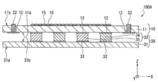
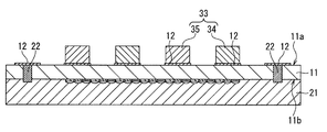
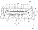
- FIG. 1 is a plan view showing a configuration example of the semiconductor device 100 according to the first embodiment of the present disclosure.
- FIG. 2 is a cross-sectional view showing a configuration example of the semiconductor device 100 according to the first embodiment of the present disclosure.
- FIG. 2 shows a cross section of FIG. 1 cut along the X1-X'1 line.
- the semiconductor device 100 shown in FIGS. 1 and 2 is, for example, a sensor device, and includes a sensor element 10 and a perche element 30.
- the sensor element 10 is, for example, a CMOS (Complementary Metal Oxide Semiconductor) image sensor or a CCD (Charge Coupled Device) image sensor.
- the sensor element 10 may be called a sensor chip.
- the sensor element 10 is provided inside the semiconductor substrate 11, the first electrode 12 provided on the lower surface 11a side of the semiconductor substrate 11, the external connection terminal 14 provided on the upper surface 11b side of the semiconductor substrate 11, and the inside of the semiconductor substrate 11. It includes a plurality of wirings 13 provided in multiple layers, a color filter layer 15 provided on the upper surface 11b of the semiconductor substrate 11, and a microlens layer 16 provided on the color filter layer 15.
- the semiconductor substrate 11 is, for example, a silicon substrate.
- the first electrode 12 is made of, for example, copper (Cu) or a Cu alloy containing Cu as a main component.
- the sensor element 10 detects light by photoelectric conversion in the pixel region AR1 in which the color filter layer 15 and the microlens layer 16 are arranged.
- the light detected by the sensor element 10 is not limited to visible light, and may be, for example, infrared rays or ultraviolet rays.
- the external connection terminal 14 is provided outside the pixel area AR1.
- the external connection terminal 14 is, for example, a bonding pad, to which a wire such as a gold wire is connected.
- the external connection terminal 14 is connected to the perche element 30 via a wiring 13 provided inside the semiconductor substrate.
- the sensor element 10 has a pair of external connection terminals 14. Of the pair of external connection terminals 14, one external connection terminal 14 is used as a positive electrode side terminal for applying a positive potential to the Pelche element 30, and the other external connection terminal 14 applies a ground potential or a negative potential to the Pelche element 30. It is used as a negative electrode side terminal. When a voltage is applied between the pair of external connection terminals 14, a current flows from one external connection terminal 14 to the other external connection terminal 14 through a thermoelectric semiconductor 33 described later of the Pelche element 30.
- the Perche element 30 has a lower substrate 31 (an example of the "first substrate” of the present disclosure) and a thermoelectric semiconductor 33 arranged between the lower substrate 31 and the semiconductor substrate 11.
- the lower substrate 31 is, for example, a ceramic substrate.
- the lower substrate 31 has a second electrode 32 provided on the upper surface 31b side facing the semiconductor substrate 11.
- the region AR2 in which the thermoelectric semiconductor 33 is arranged overlaps with the pixel region AR1 in a plan view.
- the region AR2 in which the thermoelectric semiconductor 33 is arranged overlaps the pixel region AR1 and its peripheral region AR3 in a plan view.
- the second electrode 32 is made of, for example, Cu or a Cu alloy.
- the first electrode 12 of the semiconductor substrate 11 and the second electrode 32 of the lower substrate 31 are connected to the thermoelectric semiconductor 33, respectively.
- the semiconductor substrate 11 is not only used as a substrate of the semiconductor device 100, but is also a substrate arranged on the opposite side of the lower substrate 31 with the thermoelectric semiconductor 33 interposed therebetween, and the lower substrate 31. It is also used as a substrate that sandwiches the thermoelectric semiconductor 33 between the two.
- FIG. 3 is a cross-sectional view showing a configuration example of the perche element 30 according to the first embodiment of the present disclosure.
- the thermoelectric semiconductor 33 includes a plurality of P-type thermoelectric semiconductors 34 and a plurality of N-type thermoelectric semiconductors 35.
- the P-type thermoelectric semiconductor 34 and the N-type thermoelectric semiconductor 35 are arranged between the semiconductor substrate 11 and the lower substrate 31, respectively.
- the P-type thermoelectric semiconductor 34 and the N-type thermoelectric semiconductor 35 are arranged side by side alternately at intervals in one direction.
- the first electrode 12 of the semiconductor substrate 11 is connected to the upper end of the P-type thermoelectric semiconductor 34 and the upper end of the N-type thermoelectric semiconductor 35.
- the second electrode 32 of the lower substrate 31 is connected to the lower end of the P-type thermoelectric semiconductor 34 and the lower end of the N-type thermoelectric semiconductor 35.
- the P-type thermoelectric semiconductor 34 and the N-type thermoelectric semiconductor 35 are alternately connected in series via the first electrode 12 of the semiconductor substrate 11 and the second electrode 32 of the lower substrate 31.
- the Perche element 30 when a direct current is passed from the N-type thermoelectric semiconductor 35, the semiconductor substrate 11 absorbs (endothermics) heat T1 and the lower substrate 31 releases heat T2. (Dissipate heat).
- the perche element 30 can release the heat generated by the sensor element 10 to the outside of the semiconductor device 100 via the lower substrate 31.
- the manufacturing method of the semiconductor device 100 shown in FIGS. 1 and 2 will be described.
- various devices such as a device for forming the first electrode 12, a device for attaching the thermoelectric semiconductor 33, and a wire bonding device are used.
- these devices are collectively referred to as manufacturing devices.
- at least a part of the work performed by the manufacturing apparatus may be performed by a worker.
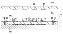
- FIG. 4A to 4E are cross-sectional views showing a method of manufacturing the semiconductor device 100 according to the first embodiment of the present disclosure.
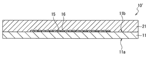
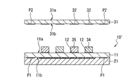
- the manufacturing apparatus manufactures the sensor wafer 10'.
- the sensor wafer 10' is a substrate before dicing in which the sensor element 10 is formed by multi-imposition.
- the first electrode 12 (see FIG. 2) is not formed.
- the first electrode 12 is formed in the process of FIG. 4C described later.
- the manufacturing apparatus attaches the support substrate 21 to the upper surface 11b side of the semiconductor substrate 11.
- the support substrate 21 protects the upper surface 11b side of the semiconductor substrate 11 including the color filter layer 15 and the microlens layer 16.
- the manufacturing apparatus uses a vapor deposition method, a sputtering method, or a CVD method to form a copper (Cu) film on the lower surface 11a side of the semiconductor substrate 11.
- the manufacturing apparatus uses photolithography to form a resist pattern having a predetermined shape on the Cu film.
- the manufacturing apparatus etches the Cu film using the resist pattern as a mask.
- the manufacturing apparatus forms the first electrode 12 from the Cu film.
- the manufacturing apparatus may form the first electrode 12 from the Cu film by using the lift-off method.
- the manufacturing apparatus may form the first electrode 12 by any method.
- the manufacturing apparatus mounts the P-type thermoelectric semiconductor 34 and the N-type thermoelectric semiconductor 35 on the first electrode 12.
- a sheet to which the P-type thermoelectric semiconductor 34 and the N-type thermoelectric semiconductor 35 are previously attached is pressed against the lower surface 11a side of the semiconductor substrate 11, and the P-type thermoelectric semiconductor 34 and the N-type thermoelectric semiconductor 34 and the N-type thermoelectric semiconductor are pressed against the first electrode 12.
- the P-type thermoelectric semiconductor 34 and the N-type thermoelectric semiconductor 35 are mounted on the first electrode 12 by joining the semiconductors 35 to each other and then removing only the sheet.
- the manufacturing apparatus may mount the P-type thermoelectric semiconductor 34 and the N-type thermoelectric semiconductor 35 on the first electrode 12.
- the P-type thermoelectric semiconductor 34 and the N-type thermoelectric semiconductor 35 may be mounted one by one on the first electrode 12.
- the manufacturing apparatus the upper surface 31b side of the lower substrate 31 is directed downward, and the second electrode 32 of the lower substrate 31 is formed into the P-type thermoelectric semiconductor 34 and the N-type thermoelectric semiconductor 35. Join each.
- the manufacturing apparatus dices the sensor wafer 10'and the lower substrate 31 to separate the semiconductor apparatus 100 into pieces. After that, the manufacturing apparatus detaches the support substrate 21 from the upper surface 11b side of the semiconductor substrate 11. Through the above steps, the semiconductor device 100 shown in FIGS. 1 and 2 is completed.
- the semiconductor device 100 includes a semiconductor substrate 11 and a Perche element 30 arranged to face the semiconductor substrate 11.
- the perche element 30 has a lower substrate 31 and a thermoelectric semiconductor 33 arranged between the lower substrate 31 and the semiconductor substrate 11.
- the semiconductor substrate 11 has a first electrode 12 provided on the lower surface 11a side facing the lower substrate 31.
- the lower substrate 31 has a second electrode 32 provided on the upper surface 31b side facing the semiconductor substrate 11.
- the first electrode 12 and the second electrode 32 are each connected to the thermoelectric semiconductor 33.
- the thermoelectric semiconductor 33 has a plurality of P-type thermoelectric semiconductors 34 and a plurality of N-type thermoelectric semiconductors 35.
- the P-type thermoelectric semiconductor 34 and the N-type thermoelectric semiconductor 35 are alternately connected in series via the first electrode 12 and the second electrode 32.
- the Perche element 30 As an upper substrate of the Perche element 30 (a substrate arranged on the opposite side of the lower substrate 31 with the thermoelectric semiconductor 33 sandwiched between them, and a substrate sandwiching the thermoelectric semiconductor 33 with the lower substrate 31).
- the semiconductor substrate 11 can also be used.
- the Perche element 30 can be integrated with the semiconductor substrate 11, and the number of parts of the semiconductor device 100 can be reduced. As a result, the thickness of the semiconductor device 100 can be reduced (reduced in height), and the semiconductor device 100 can be miniaturized.
- the heat exhaust efficiency from the semiconductor substrate 11 to the Perche element 30 is improved. Since there is no substrate (upper substrate) for supporting the thermoelectric semiconductor 33 between the semiconductor substrate 11 and the Perche element 30, heat is efficiently exhausted from the semiconductor substrate 11 to the Perche element 30. As a result, the Perche element 30 can improve the cooling performance of the semiconductor substrate 11.
- the input and output of the current to the Perche element 30 are performed not through the lead-out wiring dedicated to the Perche element drawn out to the outside of the semiconductor substrate 11, but through the wiring such as a gold wire connected to the external connection terminal 14. Since the drawer wiring dedicated to the Pelche element is not required, the space can be further reduced. As a result, the semiconductor device 100 can be further miniaturized.
- the upper substrate of the Pelche element 30, the drawer wiring dedicated to the Pelche element, and the adhesive for joining the upper substrate and the semiconductor substrate are not required, and the number of parts can be reduced. As a result, the cost of the semiconductor device 100 can be reduced.
- the warp of the semiconductor substrate 11 can be suppressed. That is, since a general resin has a coefficient of linear expansion larger than that of an adhesive base material or a device, it expands and contracts or its elastic modulus changes depending on the temperature. Therefore, it tends to cause the semiconductor substrate 11 to warp. However, in the semiconductor device 100, since there is no resin for adhesion between the semiconductor substrate 11 and the thermoelectric semiconductor 33, the warp of the semiconductor substrate 11 can be suppressed.
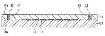
- FIG. 5 is a cross-sectional view showing the configuration of the semiconductor device 100A according to the first modification of the first embodiment of the present disclosure.
- the semiconductor substrate 11 of the semiconductor device 100A may be provided with a through electrode 22 (an example of the “first through electrode” of the present disclosure) penetrating the semiconductor substrate 11 in the thickness direction.
- the through silicon via 22 penetrates between the lower surface 11a and the upper surface 11b of the semiconductor substrate 11.
- the through electrode 22 is made of a metal such as Cu.
- the through electrode 22 may be used as an external connection terminal for applying an electric potential to the perche element 30.
- the sensor element 10 has a pair of through electrodes 22 provided in a peripheral region AR3 (see FIG. 1) located outside the pixel region AR1 (see FIG. 1).
- the upper end of the through electrode 22 is used as a bonding pad exposed on the upper surface 11b side of the semiconductor substrate 11.
- a wire such as a gold wire is connected to the bonding pad.
- the lower end of the through electrode 22 is connected to the first electrode 12 of the sensor element 10. Even with such a configuration, the semiconductor device 100A has the same effect as the above-mentioned semiconductor device 100.
- the semiconductor device 100A shown in FIG. 5 may also be provided with an external connection terminal 14 as shown in FIG. 2 in addition to the through electrode 22. Further, although not shown in FIG. 5, the wiring 13 may be provided inside the semiconductor substrate 11.
- FIG. 6A to 6E are cross-sectional views showing the manufacturing method of the semiconductor device 100A according to the first modification of the first embodiment of the present disclosure in the order of processes.
- the manufacturing method described with reference to FIGS. 4A and 4B is the same up to the step of attaching the support substrate 21 to the upper surface 11b side of the semiconductor substrate 11.
- the manufacturing apparatus turns the semiconductor substrate 11 upside down so that the lower surface 11a side of the semiconductor substrate 11 faces upward. Then, the manufacturing apparatus forms a through hole (via) H1 penetrating between the lower surface 11a and the upper surface 11b of the semiconductor substrate 11 from the lower surface 11a side of the semiconductor substrate 11. Next, the manufacturing apparatus forms the through electrode 22 inside the through hole H1. Next, as shown in FIG. 6C, the manufacturing apparatus forms the first electrode 12 on the lower surface 11a side of the semiconductor substrate 11. The lower end portion of the through electrode 22 (the upper end portion in FIG. 6C) is covered with the first electrode 12.
- the manufacturing apparatus mounts the P-type thermoelectric semiconductor 34 and the N-type thermoelectric semiconductor 35 on the first electrode 12.
- the manufacturing apparatus has a P-type thermoelectric semiconductor 34 and an N-type thermoelectric semiconductor 35 on the second electrode 32 of the lower substrate 31 with the upper surface 31b side of the lower substrate 31 facing downward. Join each.
- the manufacturing apparatus dices the sensor wafer 10'and the lower substrate 31 to separate the semiconductor apparatus 100A into pieces. After that, the manufacturing apparatus detaches the support substrate 21 from the upper surface 11b side of the semiconductor substrate 11.
- the semiconductor device 100A shown in FIG. 5 is completed.
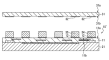
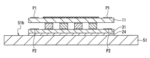
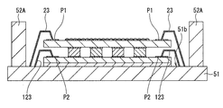
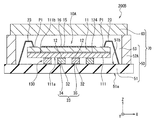
- FIG. 7 is a cross-sectional view showing the configuration of the semiconductor device 100B according to the second modification of the first embodiment of the present disclosure.
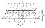
- the semiconductor device 100B includes a package main body 50 and a lid 60 attached to the upper surface side of the package main body 50.
- the package body 50 and the lid 60 constitute a package 70 that houses the sensor element 10 and the perche element 30 and seals them airtightly.
- a bonding pad P1 connected to the sensor element 10 is provided on the upper surface 111b side of the semiconductor substrate 11.
- a wire 23 is bonded to the bonding pad P1.
- the sensor element 10 can input and output a power source and a signal via the bonding pad P1 and the wire 23.
- a bonding pad P2 for inputting and outputting a current to the Pelche element 30 is provided on the upper surface 111b side of the lower substrate 11.
- the bonding pad P2 is connected to a second electrode 32 provided on the upper surface 111b side of the lower substrate 11. Further, a wire 123 is bonded to the bonding pad P2. A current is applied to the perche element 30 via the wire 123 and the bonding pad P2.
- the bonding pads P1 and P2 are composed of, for example, an Al alloy containing aluminum (Al) or Al as a main component, or a Cu alloy containing copper (Cu) or Cu as a main component.
- the wires 32 and 132 are, for example, gold wires.
- the package body 50 has a bottom portion 51 to which the lower substrate 31 of the Pelche element 30 is attached via the die bond material 24, and a wall portion 52 arranged around the bottom portion 51.
- the bottom portion 51 and the wall portion 52 are integrally formed.
- the sensor element 10 and the Pelche element 30 are arranged in the space 53 inside the package 70 surrounded by the bottom portion 51 and the wall portion 52.
- the package body 50 is made of, for example, ceramic.
- the lid 60 is made of a material that transmits light detected by the sensor element 10, and is made of, for example, a translucent glass material or a translucent resin.
- the lid 60 may have a frame (not shown) that is joined to the wall of the package body 50 without gaps.
- the frame is made of, for example, ceramic or metal.
- a bonding pad (not shown) is provided to which one end of each of the wires 23 and 123 such as a gold wire is connected.
- the bonding pad to which the wire 23 is connected and the bonding pad to which the wire 123 is connected are separated from each other and are electrically separated from each other.
- a plurality of wirings (not shown) are provided in multiple layers inside the bottom portion 51. These wirings are connected to a bonding pad provided on the upper surface 51b side of the bottom portion and a plurality of terminals (not shown) provided on the lower surface 51a side of the bottom portion 51.
- the plurality of terminals provided on the lower surface 51a side of the bottom portion 51 may be pin-shaped terminals protruding in the normal direction of the lower surface 51a, or ball-shaped terminals.
- the through electrode 22 of the sensor element 10 includes a wire 23, a bonding pad provided on the upper surface 51b side of the bottom portion 51, wiring provided inside the bottom portion 51, and a terminal provided on the lower surface 51a side of the bottom portion. It is pulled out to the outside of the package 70 via.
- the sensor element 10 and the Pelche element 30 are arranged in the space 53 inside the package 70 and are hermetically sealed.
- the semiconductor device 100B can suppress the adhesion of foreign matter to the sensor element 10, and can reduce the possibility that the operation of the sensor element 10 is affected by the foreign matter.
- FIG. 8A to 8D are cross-sectional views showing the manufacturing method of the semiconductor device 100B according to the second modification of the first embodiment of the present disclosure in the order of processes.
- the thermoelectric semiconductor 33 is attached to the lower surface 11a side of the semiconductor substrate 11, the semiconductor device 100A is separated by dicing, and then the support substrate 21 is detached with reference to FIGS. 6A to 6E. It is the same as the manufacturing method described.
- the manufacturing apparatus applies the die bond material 24 to the upper surface 51b side of the bottom portion 51 of the package body 50, as shown in FIG. 8B.
- the manufacturing apparatus attaches the lower substrate 31 to the upper surface 51b side of the bottom 51 via the die bond material 24.
- the manufacturing apparatus connects the bonding pad P1 of the sensor element 10 and the bonding pad (not shown) provided on the upper surface 51b side of the bottom portion 51 with a wire 23.
- a bonding pad provided on the upper surface 31b side of the lower substrate 31 and a bonding pad (not shown) provided on the upper surface 51b side of the bottom portion 51 are connected by a wire 123.
- the manufacturing apparatus attaches the lid 60 to the wall portion 52 of the package body 50 by means such as seam welding in a state where the lid 60 and the package body 50 are aligned with each other. As a result, the space 53 between the lid 60 and the package body 50 is airtightly sealed.
- Seam welding is a type of resistance welding, and is a method of continuous welding by rotating the electrodes while applying pressure and energizing using roller electrodes.
- the atmosphere inside the package that is, the space 53
- the atmosphere inside the package can be kept in dry air, nitrogen, or vacuum by creating an atmosphere such as dry air, nitrogen, or vacuum in the chamber provided in the seam welding apparatus. ..
- the joining between the lid 60 and the package body 50 is not limited to seam welding.
- the joining of the lid 60 and the package body 50 may be, for example, joining using an adhesive.
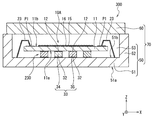
- FIG. 9 is a cross-sectional view showing the configuration of the semiconductor device 100C according to the third modification of the first embodiment of the present disclosure.
- the package body 50 included in the semiconductor device 100C has a bottom portion 51 to which the lower substrate 31 of the Pelche element 30 is attached via the die bond material 24, and a wall portion 52A arranged around the bottom portion 51.
- the bottom portion 51 and the wall portion 52A are formed separately, and are made of, for example, different materials from each other.
- the bottom 51 is made of ceramic, while the wall 52A is made of resin or metal.
- the bottom portion 51 and the wall portion 52A are joined to each other via, for example, an adhesive (not shown).
- the semiconductor device 100C has the same effect as the semiconductor device 100B. Further, as will be described in the manufacturing method described later, before the wall portion 52A is attached around the bottom portion 51, the perche element 30 and the sensor element 10 are attached to the upper surface 51b side of the bottom portion 51, or wire bonding is performed. be able to. When the sensor element 10 is attached to the package body 50, there is no wall portion 52A on the upper surface 51b side of the bottom portion 51, and the upper surface 51b of the bottom portion 51 is flat. Is easy. Therefore, the semiconductor device 100C may be able to improve the productivity as compared with the semiconductor device 100B.
- FIG. 10A to 10D are cross-sectional views showing the manufacturing method of the semiconductor device 100C according to the third modification of the first embodiment of the present disclosure in the order of processes.
- the manufacturing method described with reference to FIGS. 8A and 8B is the same up to the step of applying the die bond material 24 to the upper surface 51b side of the bottom portion 51 of the package body 50A.
- the manufacturing apparatus After applying the die bond material 24, as shown in FIG. 10B, the manufacturing apparatus attaches the lower substrate 31 to the upper surface 51b side of the bottom portion 51 via the die bond material 24.
- the manufacturing apparatus connects the bonding pad P1 of the sensor element 10 and the bonding pad (not shown) provided on the upper surface 51b side of the bottom portion 51 with a wire 23 (first). Wire bonding process).
- the manufacturing apparatus connects the bonding pad P2 of the lower substrate 31 and the bonding pad (not shown) provided on the upper surface 51b side of the bottom portion 51 with a wire 123 (second wire bonding step).
- the manufacturing apparatus attaches the wall portion 52A to the upper surface 51b side of the bottom portion 51 via an adhesive or the like.
- the first wire bonding step and the second wire bonding step may be performed after the wall portion 52A mounting step is performed.
- the manufacturing apparatus attaches the lid 60 to the wall portion 52A of the package body 50, and airtightly seals the space 53 between the lid 60 and the package body 50.
- the semiconductor device 100C shown in FIG. 9 is completed.
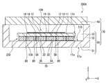
- FIG. 11 is a cross-sectional view showing the configuration of the semiconductor device 100D according to the fourth modification of the first embodiment of the present disclosure.
- the package format of the semiconductor device 100D is a wafer level chip size package.
- an insulating first spacer 25 is provided between the semiconductor substrate 11 and the lower substrate 31 and outside the region AR2 in which the thermoelectric semiconductor 33 is arranged.
- the first spacer 25 is an insulating frame that surrounds the region AR2 in which the thermoelectric semiconductor 33 is arranged without any gap in a plan view.
- the first spacer 25 may be made of an insulating resin or a ceramic.
- the upper end of the first spacer 25 is bonded to the lower surface 11a of the semiconductor substrate 11, and the lower end of the first spacer 25 is bonded to the upper surface 31b of the lower substrate 31.
- a through wiring 26 that penetrates the first spacer 25 in the Z-axis direction (thickness direction of the semiconductor device 100) is provided.
- the through wiring 26 is made of a metal such as Cu.
- the through wiring 26 is connected to a wiring 13 provided inside the semiconductor substrate 11 and a through electrode 36 penetrating between the lower surface 31a and the upper surface 31b of the lower substrate 31, respectively.
- the through electrode 36 is made of a metal such as Cu.
- a rewiring layer 37 (an example of the "second rewiring layer” of the present disclosure) is provided on the lower surface 31a side, which is the opposite side of the surface facing the semiconductor substrate 11.
- the rewiring layer 37 has, for example, a wiring 38 provided in multiple layers and an insulating layer 39 that insulates between the wiring 38 of one layer and the wiring 38 of the other layer.
- the wiring 38 is made of a metal such as Cu.
- the insulating layer 39 is made of, for example, a solder resist.
- a plurality of bump electrodes 40 are provided on the lowermost surface of the rewiring layer 37.
- the bump electrode 40 is connected to the wiring 38.
- the bump electrode 40 is made of, for example, a solder ball.
- a second spacer 45 is provided between the upper surface 11b of the semiconductor substrate 11 and the lid 60 and outside the region where the color filter layer 15 and the microlens layer 16 are arranged.
- the second spacer 45 is an insulating frame that surrounds the region where the color filter layer 15 and the microlens layer 16 are arranged without any gap in a plan view.
- the second spacer 45 is provided so as to overlap the first spacer 25 in the Z-axis direction via the semiconductor substrate 11.
- the second spacer 45 may be made of an insulating resin or a ceramic.
- the upper end of the second spacer 45 is bonded to the lid 60, and the lower end of the second spacer 45 is bonded to the upper surface 11b of the semiconductor substrate 11.
- the space between the semiconductor substrate 11 and the lower substrate 31 is hermetically sealed by the frame-shaped first spacer 25. Further, the space between the semiconductor substrate 11 and the lid 60 is hermetically sealed with a frame-shaped second spacer 45.
- the electrical connection between the semiconductor substrate 11 and the lower substrate 31 is made not through a wire such as a gold wire, but through a through wiring 26 in the first spacer 25. Since the semiconductor device 100D is a wafer level chip size package and does not require wires, it can be further thinned and miniaturized.
- the space between the semiconductor substrate 11 and the lid 60 and surrounded by the second spacer 45 may be hollow and may be filled with a translucent resin (that is, a transparent resin). May be good.
- FIG. 12A to 12F are cross-sectional views showing the manufacturing method of the semiconductor device 100D according to the fourth modification of the first embodiment of the present disclosure in the order of processes.
- the manufacturing method described with reference to FIGS. 6A and 6B is the same up to the step of forming the sensor wafer 10'formed by the sensor element 10 by multi-imposition and forming the through electrode 22 on the sensor wafer 10'. Is.
- the manufacturing apparatus After forming the through silicon via 22, the manufacturing apparatus forms the second spacer 45 on the upper surface 11b side of the sensor wafer 10'.
- the second spacer 45 may be formed by using a wafer process, or the second spacer 45 prepared in advance may be attached to the upper surface 11b side via an adhesive or the like.
- the manufacturing apparatus mounts the lid 60 on the second spacer 45. As a result, the space between the semiconductor substrate 11 and the lid 60 is hermetically sealed.
- the semiconductor substrate 11 is turned upside down so that the lid 60 faces downward, and the first electrode 12 is placed on the lower surface 11a side (upper side in FIG. 12C) of the semiconductor substrate 11.
- the manufacturing apparatus forms a first spacer 25 on the lower surface 11a side of the semiconductor substrate 11, and joins the through wiring 26 located inside the first spacer 25 to the through electrode 22 of the semiconductor substrate 11.
- the manufacturing apparatus mounts the P-type thermoelectric semiconductor 34 and the N-type thermoelectric semiconductor 35 on the first electrode 12.
- the upper surface 31b side of the lower substrate 31 is directed downward, and the second electrode 32 of the lower substrate 31 is formed into the P-type thermoelectric semiconductor 34 and the N-type thermoelectric semiconductor 35.
- the through electrode 36 of the lower substrate 31 is joined to the through wiring 26 located inside the first spacer 25.
- the manufacturing apparatus forms a rewiring layer 37 on the lower surface 31a side of the lower substrate 31.
- the manufacturing apparatus uses, for example, a semi-additive method or a subtractive method to form the rewiring layer 37.
- the manufacturing apparatus connects the wiring 38 to the through electrode 36 of the lower substrate 31.
- the manufacturing apparatus forms a plurality of bump electrodes 40 (see FIG. 11) on the lowermost surface (the uppermost surface in FIG. 12F) of the rewiring layer 37.
- the sensor wafer 10' is diced together with the lower substrate 31.
- FIG. 13 is a cross-sectional view showing the configuration of the semiconductor device 100E according to the fifth modification of the first embodiment of the present disclosure.
- FIG. 14 is a plan view showing the arrangement of the conductor 80 according to the fifth modification of the first embodiment of the present disclosure.
- the semiconductor device 100E is arranged between the P-type thermoelectric semiconductor 34 and the N-type thermoelectric semiconductor 35, and is electrically separated from the P-type thermoelectric semiconductor 34 and the N-type thermoelectric semiconductor 35, respectively.
- the conductor 80 is provided.
- the conductor 80 is arranged adjacent to the P-type thermoelectric semiconductor 34 and the N-type thermoelectric semiconductor 35 at intervals.
- the conductor 80 is a connection terminal for connecting the semiconductor substrate 11 and the rewiring layer 37.
- the conductor 80 penetrates between the upper surface 31b and the lower surface 31a of the lower substrate 31.
- the lower end of the conductor 80 is connected to the wiring 38 of the rewiring layer 37.
- an electrode 18 is provided on the lower surface 11a side of the semiconductor substrate 11.
- the electrode 18 is provided at a position away from the first electrode 12, and is electrically separated from the first electrode 12.
- the upper end of the conductor 80 is connected to the electrode 18.
- the conductor 80 connects the semiconductor substrate 11 and the rewiring layer 37 via the electrode 18.
- the conductor 80 is used as a signal line or a power supply line between the semiconductor substrate 11 and the rewiring layer 37.
- the conductor 80 connects the semiconductor substrate 11 and the rewiring layer 37 without bypassing the Perche element 30. Since the semiconductor device 100E can shorten the wiring length between the semiconductor substrate 11 and the rewiring layer 37, it is possible to reduce the impedance.
- an insulating resin may be filled between the semiconductor substrate 11 and the lower substrate 31. Since the conductor 80 is supported from the horizontal direction (direction parallel to the XY plane) by the resin between the semiconductor substrate 11 and the lower substrate 31, the conductor 80 with respect to the semiconductor substrate 11 and the lower substrate 31 Bond strength is improved.
- the space between the semiconductor substrate 11 and the lid 60 and surrounded by the second spacer 45 may be hollow or filled with a transparent resin. It may have been done.
- the semiconductor device is a sensor device including the color filter layer 15 and the microlens layer 16 has been described.
- the semiconductor device is not limited to the sensor device.
- the semiconductor device according to the first embodiment may be an integrated circuit (IC) or a large-scale integrated circuit (LSI) that executes an arbitrary function.
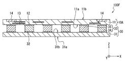
- FIG. 15 is a cross-sectional view showing the configuration of the semiconductor device 100F according to the sixth modification of the first embodiment of the present disclosure.
- the semiconductor device 100F shown in FIG. 15 is an IC or an LSI, and includes an IC element 10A and a Perche element 30.
- the IC element 10A may be called an IC chip.
- the IC element 10A is provided inside the semiconductor substrate 11, the first electrode 12 provided on the lower surface 11a side of the semiconductor substrate 11, the external connection terminal 14 provided on the upper surface 11b side of the semiconductor substrate 11, and the inside of the semiconductor substrate 11.
- a plurality of wirings 13 provided in multiple layers are provided.
- the perche element 30 has a lower substrate 31 and a thermoelectric semiconductor 33 arranged between the lower substrate 31 and the semiconductor substrate 11.
- the first electrode 12 of the semiconductor substrate 11 and the second electrode 32 of the lower substrate 31 are connected to the thermoelectric semiconductor 33, respectively.
- the semiconductor substrate 11 is used not only as a substrate of the semiconductor device 100F, but also as an upper substrate of the Perche element 30.
- the semiconductor substrate 11 is also used as the upper substrate of the Perche element 30.
- the perche element 30 is integrated with the semiconductor substrate 11, and the number of parts can be reduced. As a result, the thickness of the semiconductor device 100F can be reduced, and the size of the semiconductor device 100F can be reduced.
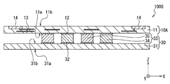
- FIG. 16 is a cross-sectional view showing the configuration of the semiconductor device 100G according to the modified example 7 of the first embodiment of the present disclosure.
- the thermoelectric semiconductor 33 is arranged below the central portion of the semiconductor substrate 11, but the thermoelectric semiconductor 33 is not arranged below the outer peripheral portion of the semiconductor substrate 11. ..
- the thermoelectric semiconductor 33 is unevenly arranged below the central portion of the semiconductor substrate 11.
- thermoelectric semiconductor 33 when the semiconductor substrate 11 is a silicon substrate, silicon has excellent thermal conductivity, so that a sufficient cooling effect can be obtained.
- the thermoelectric semiconductor 33 unevenly below the central portion of the semiconductor substrate 11, an empty space is created below the outer peripheral portion of the semiconductor substrate 11.
- the conductor 80 shown in FIG. 13 may be provided in this empty space.
- FIG. 17 is a cross-sectional view showing the configuration of the semiconductor device 100H according to the modified example 8 of the first embodiment of the present disclosure.
- the semiconductor device 100H shown in FIG. 17 is an embodiment in which the rewiring layer 37 and the bump electrode 40 are provided on the semiconductor device 100F shown in FIG.
- the rewiring layer 137 (the "first rewiring layer” of the present disclosure) is on the upper surface 11b side opposite to the surface facing the lower substrate 31. An example) is provided.
- the rewiring layer 137 has, for example, a wiring 138 provided in multiple layers and an insulating layer 139 that insulates between the wiring 138 of one layer and the wiring 138 of the other layer. Further, a plurality of bump electrodes 140 are provided on the uppermost surface of the rewiring layer 137. The bump electrode 140 is connected to the wiring 138. The bump electrode 140 is made of, for example, a solder ball. In the semiconductor device 100H, a current can be passed through the Pelche element 30 via the bump electrode 140.
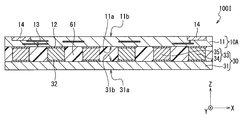
- FIG. 18 is a cross-sectional view showing the configuration of the semiconductor device 100I according to the ninth modification of the first embodiment of the present disclosure.
- an insulating resin 61 is filled between the semiconductor substrate 11 and the lower substrate 31.
- the resin 61 seals the semiconductor substrate 11 and the lower substrate 31 without a gap.
- the resin 61 is in close contact with the side surface of the thermoelectric semiconductor 33, and prevents the thermoelectric semiconductor from being exposed to the outside air or moisture. Further, the resin 61 supports the thermoelectric semiconductor 33 from the horizontal direction (direction parallel to the XY plane). As a result, the bonding strength of the thermoelectric semiconductor 33 with respect to the semiconductor substrate 11 and the lower substrate 31 is improved.
- FIG. 19 is a cross-sectional view showing the configuration of the semiconductor device 100J according to the modified example 10 of the first embodiment of the present disclosure.
- the semiconductor device 100J shown in FIG. 19 is an embodiment in which the rewiring layer 137 and the bump electrode 140 are provided on the semiconductor device 100I shown in FIG.
- a current can be passed through the Perche element 30 via the bump electrode 140.
- FIG. 20 is a cross-sectional view showing the configuration of the semiconductor device 100K according to the modified example 11 of the first embodiment of the present disclosure.
- the semiconductor device 100K includes a package main body 50 and a lid 60 attached to the upper surface side of the package main body 50.
- the package 70 is composed of the package body 50 and the lid 60.
- the semiconductor device 100K the IC element 10A and the Pelche element 30 are arranged in the space 53 inside the package 70 and are hermetically sealed. As a result, the semiconductor device 100K can suppress the adhesion of foreign matter to the IC element 10A, and can reduce the possibility that the operation of the IC element 10A is affected by the foreign matter.
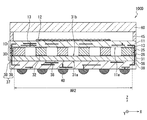
- FIG. 21 is a cross-sectional view showing a configuration example of the semiconductor device 200 according to the second embodiment of the present disclosure.
- the semiconductor device 200 shown in FIG. 21 is, for example, a sensor device, and includes a sensor element 10, a perche element 130, and a package 70.
- the sensor element 10 is, for example, a CMOS image sensor or a CCD image sensor.
- the perche element 130 has an upper substrate 111 (an example of the "second substrate” of the present disclosure) and a thermoelectric semiconductor 33 arranged between the upper substrate 111 and the wiring substrate.
- the upper substrate 111 is, for example, a ceramic substrate.
- the first electrode 12 is provided on the lower surface 111a side of the upper substrate 111.
- the upper surface 111b of the upper substrate 111 is fixed to the lower surface 11a of the semiconductor substrate 11 via the die bond material 124.
- a bonding pad P1 connected to the sensor element 10 is provided on the upper surface 111b side of the semiconductor substrate 11.
- a wire 23 is bonded to the bonding pad P1.
- the sensor element 10 can input and output a power source and a signal via the bonding pad P1 and the wire 23.
- the package 70 includes a package body 50 and a lid 60 attached to the upper surface side of the package body 50.
- the sensor element 10 and the Pelche element 130 are hermetically sealed by the package body 50 and the lid 60.
- the package body 50 has a bottom portion 51 (an example of the “wiring board” of the present disclosure) to which the thermoelectric semiconductor 33 of the Pelche element 130 is attached, and a wall portion 52 arranged around the bottom portion 51.
- the bottom portion 51 and the wall portion 52 are integrally formed.
- the sensor element 10 and the Pelche element 130 are arranged in the space 53 inside the package 70 surrounded by the bottom portion 51 and the wall portion 52.
- the second electrode 32 is provided on the upper surface 51b side of the bottom portion 51 of the package body 50.
- the first electrode 12 provided on the upper substrate 111 and the second electrode 32 provided on the bottom 51 are connected to the thermoelectric semiconductor 33, respectively.
- the bottom portion 51 is not only used as a part of the package body 50, but is also a substrate arranged on the lower substrate of the Pelche element 30A (a substrate arranged on the opposite side of the upper substrate 111 with the thermoelectric semiconductor 33 interposed therebetween, and with the upper substrate 111. It is also used as a substrate that sandwiches the thermoelectric semiconductor 33 between them).
- wiring for inputting and outputting a current to the Pelche element 130 is provided.
- This wiring is connected to the second electrode 32.
- This wiring is formed at the same time as, for example, the second electrode 32 in the same process.
- 22A to 22D are cross-sectional views showing a method of manufacturing the semiconductor device 200 according to the second embodiment of the present disclosure.
- the manufacturing apparatus has a second electrode 32 on the upper surface 51b side of the bottom portion 51 of the package body 50, and wiring (not shown) for inputting and outputting a current to the Pelche element 130.
- the manufacturing apparatus mounts the P-type thermoelectric semiconductor 34 and the N-type thermoelectric semiconductor 35 on the second electrode 32.
- the manufacturing apparatus mounts the upper substrate 111 on the P-type thermoelectric semiconductor 34 and the N-type thermoelectric semiconductor 35.
- the first electrode 12 provided on the lower surface 111a side of the upper substrate 111 is joined to the P-type thermoelectric semiconductor 34 and the N-type thermoelectric semiconductor 35, respectively.
- the manufacturing apparatus prepares the color filter layer 15, the microlens layer 16, and the semiconductor substrate 11 on which the bonding pad P1 is formed on the upper surface 11b side. Then, the manufacturing apparatus attaches the lower surface 11a side of the semiconductor substrate 11 to the upper surface 111b side of the upper substrate 111 via the die bond material 124. Next, the manufacturing apparatus connects the bonding pad P1 of the sensor element 10 and the bonding pad (not shown) provided on the upper surface 51b side of the bottom portion 51 with a wire 23.
- the manufacturing apparatus attaches the lid 60 to the wall portion 52 of the package body 50. As a result, the space 53 between the lid 60 and the package body 50 is airtightly sealed. Through the above steps, the semiconductor device 200 shown in FIG. 21 is completed.
- the semiconductor device 200 includes a semiconductor substrate 11 and a Perche element 130 arranged to face the semiconductor substrate 11.
- the perche element 130 has an upper substrate 111 and a thermoelectric semiconductor 33 arranged between the bottom 51 of the package body 50 and the upper substrate 111.
- the upper substrate 111 has a first electrode 12 provided on the lower surface 111a side facing the bottom 51 of the package body 50.
- the bottom portion 51 of the package main body 50 has a second electrode 32 provided on the upper surface 111b side facing the upper substrate 111.
- the first electrode 12 and the second electrode 32 are each connected to the thermoelectric semiconductor 33.
- the package main body is used as a lower substrate of the Pelche element 130 (a substrate arranged on the opposite side of the upper substrate 111 with the thermoelectric semiconductor interposed therebetween and sandwiching the thermoelectric semiconductor with the upper substrate 111).
- the bottom 51 of 50 can also be used.
- the perche element 130 can be integrated with the bottom portion 51, and the number of parts of the semiconductor device 200 can be reduced. As a result, the thickness of the semiconductor device 200 can be reduced (reduced in height), and the semiconductor device 200 can be miniaturized.
- the Perche element 130 can improve the cooling performance of the semiconductor substrate 11.
- the input and output of the current to the Pelche element 130 are performed not through the lead-out wiring dedicated to the Pelche element drawn out to the outside of the semiconductor substrate 11, but through the wiring provided at the bottom 51. Since the drawer wiring dedicated to the Pelche element is not required, the space can be further reduced. As a result, the semiconductor device 200 can be further miniaturized.
- the lower substrate of the Pelche element 30, the drawer wiring dedicated to the Pelche element, and the adhesive for joining the lower substrate and the bottom are not required, and the number of parts can be reduced. As a result, the cost of the semiconductor device 200 can be reduced.
- the warp of the semiconductor substrate 11 can be suppressed. That is, since a general resin has a coefficient of linear expansion larger than that of an adhesive base material or a device, it expands and contracts or its elastic modulus changes depending on the temperature. Therefore, it tends to cause the semiconductor substrate 11 to warp. However, in the semiconductor device 200, since there is no resin for adhesion between the thermoelectric semiconductor 33 and the bottom portion 51, the warp of the semiconductor substrate 11 can be suppressed.
- FIG. 23 is a cross-sectional view showing the configuration of the semiconductor device 200A according to the first modification of the second embodiment of the present disclosure.
- the package body 50 included in the semiconductor device 200A has a bottom portion 51 to which the lower substrate 31 of the Pelche element 30 is attached via the die bond material 24, and a wall portion 52A arranged around the bottom portion 51.
- the bottom portion 51 and the wall portion 52A are formed separately, and are made of, for example, different materials from each other.
- the bottom 51 is made of ceramic, while the wall 52A is made of resin or metal.
- the bottom portion 51 and the wall portion 52A are joined to each other via, for example, an adhesive (not shown).
- the semiconductor device 200A has the same effect as the semiconductor device 200. Further, as will be described in the manufacturing method described later, the perche element 30A and the sensor element 10 can be attached to the upper surface 51b side of the bottom portion 51 before the wall portion 52A is attached around the bottom portion 51. When the sensor element 10 is attached, there is no wall portion 52A on the upper surface 51b side of the bottom portion 51, and the upper surface 51b of the bottom portion 51 is flat, so that the perche element 30A and the sensor element 10 can be easily attached. Therefore, the semiconductor device 200A may be able to improve the productivity as compared with the semiconductor device 200.
- 24A to 24D are cross-sectional views showing the manufacturing method of the semiconductor device 200A according to the first modification of the second embodiment of the present disclosure in the order of processes.
- the manufacturing apparatus forms a second electrode 32 and a wiring (not shown) for inputting and outputting a current to the Pelche element 130 on the upper surface 51b side of the bottom portion 51.
- the manufacturing apparatus mounts the P-type thermoelectric semiconductor 34 and the N-type thermoelectric semiconductor 35 on the second electrode 32.
- the manufacturing apparatus mounts the upper substrate 111 on the P-type thermoelectric semiconductor 34 and the N-type thermoelectric semiconductor 35.
- the first electrode 12 provided on the lower surface 111a side of the upper substrate 111 is joined to the P-type thermoelectric semiconductor 34 and the N-type thermoelectric semiconductor 35, respectively.
- the manufacturing apparatus prepares the semiconductor substrate 11 in which the color filter layer 15 and the microlens layer 16 are formed on the upper surface 11b side. Then, the manufacturing apparatus attaches the lower surface 11a side of the semiconductor substrate 11 to the upper surface 111b side of the upper substrate 111 via the die bonding material 124. Next, the manufacturing apparatus connects the bonding pad P1 of the sensor element 10 and the bonding pad (not shown) provided on the upper surface 51b side of the bottom portion 51 with a wire 23.
- the manufacturing apparatus attaches the wall portion 52A to the upper surface 51b side of the bottom portion 51 via an adhesive or the like.
- the wire bonding step may be performed after the wall portion 52A mounting step is performed.
- the manufacturing apparatus attaches the lid 60 to the wall portion 52A of the package main body 50, and airtightly seals the space 53 between the lid 60 and the package main body 50.
- FIG. 25 is a cross-sectional view showing the configuration of the semiconductor device 200B according to the second modification of the second embodiment of the present disclosure.
- the package main body 50 has a bottom portion 51A (an example of the “wiring board” of the present disclosure) and a wall portion 52A arranged around the bottom portion 51A.
- the bottom portion 51A is a wiring board made of a material other than ceramic, for example, an organic substrate made of an organic material, a glass substrate, a mold substrate made of a mold resin, and an LCP made of an LCP (liquid crystal polymer).
- the semiconductor device 200B has the same effect as the semiconductor device 200A.
- the semiconductor substrate on which the sensor element or the IC element is formed may be used as the upper substrate of the Pelche element, and the wiring board may be used as the lower substrate of the Pelche element. That is, the upper and lower substrates of the Pelche element may be shared with other substrates other than the Pelche element.
- FIG. 26 is a cross-sectional view showing a configuration example of the semiconductor device 300 according to the third embodiment of the present disclosure.
- the semiconductor device 300 shown in FIG. 26 is, for example, a sensor device, and includes a sensor element 10, a Pelche element 230, and a package 70.
- the sensor element 10 is, for example, a CMOS image sensor or a CCD image sensor.
- the Perche element 230 has a thermoelectric semiconductor 33 arranged between the semiconductor substrate 11 and the bottom portion 51 of the package body 50 (an example of the "wiring substrate” of the present disclosure).
- the first electrode 12 is provided on the lower surface 11a side of the semiconductor substrate 11.
- a second electrode 32 is provided on the upper surface 51b side of the bottom portion 51 of the package body 50.
- the first electrode 12 and the second electrode 32 are connected to the thermoelectric semiconductor 33, respectively.
- the semiconductor substrate 11 can also be used as the upper substrate of the Pelche element 230, and the bottom portion 51 of the package body 50 can also be used as the lower substrate of the Pelche element 230.
- the Perche element 230 can be integrated with the semiconductor substrate 11 and the bottom 51, and the number of parts of the semiconductor device 300 can be reduced. As a result, the thickness of the semiconductor device 300 can be reduced (reduced in height), and the semiconductor device 300 can be miniaturized.
- the heat exhaust efficiency from the semiconductor substrate 11 to the bottom portion 51 is improved. Since there is no substrate (upper substrate) for supporting the thermoelectric semiconductor 33 between the semiconductor substrate 11 and the Perche element 30, heat is efficiently exhausted from the semiconductor substrate 11 to the Perche element 230. Further, since there is no substrate (lower substrate) for supporting the thermoelectric semiconductor 33 between the Perche element 130 and the bottom portion 51, heat is efficiently exhausted from the Perche element 230 to the bottom portion 51. As a result, the Perche element 230 can improve the cooling performance of the semiconductor substrate 11.
- the semiconductor device 300 is downsized by eliminating the need for the lead wiring dedicated to the Pelche element, the cost is reduced by reducing the number of parts, and the warp of the semiconductor substrate 11 is improved by improving the heat exhaust property. It has various effects such as suppression of.
- FIG. 27 is a cross-sectional view showing the configuration of the semiconductor device 300A according to the modified example of the third embodiment of the present disclosure.
- the semiconductor device 300A is arranged between the P-type thermoelectric semiconductor 34 and the N-type thermoelectric semiconductor 35, and is electrically separated from the P-type thermoelectric semiconductor 34 and the N-type thermoelectric semiconductor 35, respectively. It has a body 80.
- the conductor 80 is a connection terminal for connecting the electrode 18 provided on the lower surface side of the semiconductor substrate 11 and the electrode 58 provided on the bottom 51 of the package body 50.
- the electrode 18 is provided at a position away from the first electrode 12, and is electrically separated from the first electrode 12.
- the electrode 58 is provided at a position away from the second electrode 32, and is electrically separated from the second electrode 32.
- the conductor 80 connects the semiconductor substrate 11 and the bottom portion 51 of the package body 50 via the electrodes 18 and 58.
- the conductor 80 is used as a signal line or a power supply line between the semiconductor substrate 11 and the bottom portion 51.
- the conductor 80 does not bypass the Pelche element 230 and connects between the semiconductor substrate 11 and the bottom 51. Since the semiconductor device 300A can shorten the wiring length between the semiconductor substrate 11 and the bottom portion 51, it is possible to reduce the impedance.
- an insulating resin (not shown) may be filled between the semiconductor substrate 11 and the bottom portion 51. Since the conductor 80 is supported from the horizontal direction (direction parallel to the XY plane) by the resin between the semiconductor substrate 11 and the bottom portion 51, the bonding strength of the conductor 80 to the semiconductor substrate 11 and the bottom portion 51 is improved. To do.
- the present disclosure may also have the following structure.
- the perche element is 1st board and It has a thermoelectric semiconductor arranged between the first substrate and the semiconductor substrate, and has.
- the semiconductor substrate has a first electrode provided on the surface side facing the first substrate.
- the first substrate has a second electrode provided on the surface side facing the semiconductor substrate.
- (2) Semiconductor substrate and The wiring board facing the semiconductor board and A perche element arranged between the semiconductor substrate and the wiring substrate is provided.
- the perche element is With the second board It has a thermoelectric semiconductor arranged between the wiring board and the second board.
- the second substrate has a first electrode provided on the surface side facing the wiring board.
- the wiring board has a second electrode provided on the surface side facing the second board.
- (3) Semiconductor substrate and The wiring board facing the semiconductor board and A perche element arranged between the semiconductor substrate and the wiring substrate is provided.
- the perche element is It has a thermoelectric semiconductor arranged between the semiconductor substrate and the wiring board, and has The semiconductor substrate has a first electrode provided on the surface side facing the wiring board.
- the wiring board has a second electrode provided on the surface side facing the semiconductor board.
- a semiconductor device in which the first electrode and the second electrode are each connected to a thermoelectric semiconductor.
- a first through electrode that penetrates the semiconductor substrate in the thickness direction is further provided.
- the first through electrode is connected to the first electrode.
- a package for accommodating the semiconductor substrate and the Pelche element and airtightly sealing the semiconductor substrate is further provided.
- the thermoelectric semiconductor is With multiple first thermoelectric semiconductors, It has a plurality of second thermoelectric semiconductors having a conductive type different from that of the first thermoelectric semiconductor.
- thermoelectric semiconductor and the second thermoelectric semiconductor are alternately connected in series via the first electrode and the second electrode.
- the semiconductor device according to any one of (1) to (7) above. (9) The semiconductor device according to (8), further comprising a first thermoelectric semiconductor and a conductor arranged adjacent to each other at intervals from the second thermoelectric semiconductor. (10) The semiconductor device according to (8) or (9), further comprising an insulating resin filled between the first thermoelectric semiconductor and the second thermoelectric semiconductor.
- the present disclosure may have the following structure.
- (11) Semiconductor substrate and A perche element arranged on one surface side of the semiconductor substrate is provided.
- the perche element is With thermoelectric semiconductors It has a first substrate arranged on the opposite side of the semiconductor substrate with the thermoelectric semiconductor interposed therebetween.
- (12) Semiconductor substrate and The wiring board facing the semiconductor board and A perche element arranged between the semiconductor substrate and the wiring substrate is provided.
- the perche element is With thermoelectric semiconductors It has a second substrate arranged on the opposite side of the wiring board with the thermoelectric semiconductor interposed therebetween.
- thermoelectric semiconductor A semiconductor device in which the wiring board is also used as the first board that sandwiches and supports the thermoelectric semiconductor with the second board.
- (13) Semiconductor substrate and The wiring board facing the semiconductor board and A perche element arranged between the semiconductor substrate and the wiring substrate is provided.
- the perche element is Has a thermoelectric semiconductor
Landscapes
- Cooling Or The Like Of Semiconductors Or Solid State Devices (AREA)
- Engineering & Computer Science (AREA)
- Microelectronics & Electronic Packaging (AREA)
Abstract
Description
(構成)
図1は、本開示の実施形態1に係る半導体装置100の構成例を示す平面図である。図2は、本開示の実施形態1に係る半導体装置100の構成例を示す断面図である。図2は、図1をX1-X’1線で切断した断面を示している。図1及び図2に示す半導体装置100は、例えばセンサ装置であり、センサ素子10と、ペルチェ素子30と、を備える。
図4Aから図4Eは、本開示の実施形態1に係る半導体装置100の製造方法を示す断面図である。図4Aに示すように、製造装置は、センサウェハ10’を製造する。センサウェハ10’は、センサ素子10が多面付けで形成された、ダイシング前の基板である。なお、図4Aの工程において、第1電極12(図2参照)は未形成である。第1電極12は、後述の図4Cの工程で形成される。
図5は、本開示の実施形態1の変形例1に係る半導体装置100Aの構成を示す断面図である。図5に示すように、半導体装置100Aの半導体基板11には、半導体基板11を厚さ方向に貫く貫通電極22(本開示の「第1貫通電極」の一例)が設けられていてもよい。貫通電極22は、半導体基板11の下面11aと上面11bとの間を貫いている。貫通電極22は、例えばCu等の金属で構成されている。
図7は、本開示の実施形態1の変形例2に係る半導体装置100Bの構成を示す断面図である。図7に示すように、半導体装置100Bは、パッケージ本体50と、パッケージ本体50の上面側に取り付けられたリッド60とを備える。パッケージ本体50とリッド60とによって、センサ素子10とペルチェ素子30とを収容して気密に封止するパッケージ70が構成されている。
図9は、本開示の実施形態1の変形例3に係る半導体装置100Cの構成を示す断面図である。図9に示す半導体装置100Cにおいて、図7に示した半導体装置100Bとの違いは、パッケージ本体50の構造にある。半導体装置100Cが有するパッケージ本体50は、ダイボンド材24を介してペルチェ素子30の下側基板31が取り付けられる底部51と、底部51の周囲に配置された壁部52Aとを有する。底部51と壁部52Aは別々に形成されており、例えば互いに異なる材料で構成されている。一例を挙げると、底部51はセラミックで構成されているのに対して、壁部52Aは樹脂又は金属で構成されている。底部51と壁部52Aは、例えば、接着剤(図示せず)などを介して互いに接合されている。
図11は、本開示の実施形態1の変形例4に係る半導体装置100Dの構成を示す断面図である。図11に示すように、半導体装置100Dのパッケージ形式は、ウェハレベルチップサイズパッケージである。半導体装置100Dにおいて、半導体基板11と下側基板31との間であって、熱電半導体33が配置される領域AR2の外側には、絶縁性の第1スペーサ25が設けられている。第1スペーサ25は、熱電半導体33が配置される領域AR2を平面視で隙間なく囲む絶縁性の枠体である。第1スペーサ25は絶縁性の樹脂で構成されていてもよいし、セラミックで構成されていてもよい。第1スペーサ25の上端は半導体基板11の下面11aに接合され、第1スペーサ25の下端は下側基板31の上面31bに接合されている。
図13は、本開示の実施形態1の変形例5に係る半導体装置100Eの構成を示す断面図である。図14は、本開示の実施形態1の変形例5に係る導電体80の配置を示す平面図である。図13及び図14に示すように、半導体装置100Eは、P型熱電半導体34とN型熱電半導体35との間に配置され、P型熱電半導体34及びN型熱電半導体35からそれぞれ電気的に分離された導電体80を備える。導電体80は、P型熱電半導体34及びN型熱電半導体35とそれぞれ間隔を置いて隣り合って配置されている。
上記の実施形態1とその変形例1から5では、半導体装置が、カラーフィルタ層15及びマイクロレンズ層16を備えるセンサ装置である場合を説明した。しかしながら、本開示の第1実施形態において、半導体装置はセンサ装置に限定されない。第1実施形態に係る半導体装置は、任意の機能を実行する集積回路(IC)又は大規模集積回路(LSI)であってもよい。
図16は、本開示の実施形態1の変形例7に係る半導体装置100Gの構成を示す断面図である。図16に示すように、半導体装置100Gでは、半導体基板11の中央部の下方には熱電半導体33が配置されているが、半導体基板11の外周部の下方には熱電半導体33は配置されていない。熱電半導体33は、半導体基板11の中央部の下方に偏って配置されている。
図17は、本開示の実施形態1の変形例8に係る半導体装置100Hの構成を示す断面図である。図17に示す半導体装置100Hは、図15に示した半導体装置100Fに再配線層37とバンプ電極40とを設けた態様である。図17に示すように、半導体装置100Hでは、半導体基板11において、下側基板31と向かい合う面の反対側である上面11b側に、再配線層137(本開示の「第1再配線層」の一例)が設けられている。再配線層137は、例えば、多層に設けられた配線138と、一の層の配線138と他の層の配線138との間を絶縁する絶縁層139とを有する。また、再配線層137の最上面には、複数のバンプ電極140が設けられている。バンプ電極140は、配線138に接続している。バンプ電極140は、例えばはんだボールで構成されている。半導体装置100Hでは、バンプ電極140を介してペルチェ素子30に電流を流すことができる。
図18は、本開示の実施形態1の変形例9に係る半導体装置100Iの構成を示す断面図である。図18に示すように、半導体装置100Iでは、半導体基板11と下側基板31との間に絶縁性の樹脂61が充填されている。樹脂61によって、半導体基板11と下側基板31との間は隙間なく封止されている。樹脂61は、熱電半導体33の側面と密着しており、熱電半導体が外気や水分に晒されることを防いでいる。また、樹脂61は、熱電半導体33を水平方向(X-Y平面に平行な方向)から支持している。これにより、半導体基板11及び下側基板31に対する熱電半導体33の接合強度の向上が図られている。
図19は、本開示の実施形態1の変形例10に係る半導体装置100Jの構成を示す断面図である。図19に示す半導体装置100Jは、図18に示した半導体装置100Iに再配線層137とバンプ電極140とを設けた態様である。半導体装置100Jでは、バンプ電極140を介してペルチェ素子30に電流を流すことができる。
図20は、本開示の実施形態1の変形例11に係る半導体装置100Kの構成を示す断面図である。図20に示すように、半導体装置100Kは、パッケージ本体50と、パッケージ本体50の上面側に取り付けられたリッド60とを備える。パッケージ本体50とリッド60とによって、パッケージ70が構成されている。
上記の実施形態1とその変形例では、センサ素子又はIC素子が形成された半導体基板を、ペルチェ素子の上側基板に兼用する態様を示した。しかしながら、本開示の実施形態はこれに限定されない。本開示の実施形態では、配線基板をペルチェ素子の下側基板に兼用してもよい。
図21は、本開示の実施形態2に係る半導体装置200の構成例を示す断面図である。図21に示す半導体装置200は、例えばセンサ装置であり、センサ素子10と、ペルチェ素子130と、パッケージ70と、を備える。上述したように、センサ素子10は、例えば、CMOSイメージセンサ又はCCDイメージセンサである。
次に、図21に示した半導体装置200の製造方法について説明する。図22Aから図22Dは、本開示の実施形態2に係る半導体装置200の製造方法を示す断面図である。図22Aに示すように、製造装置は、パッケージ本体50の底部51の上面51b側に第2電極32と、ペルチェ素子130への電流の入力及び出力を行うための配線(図示せず)とを形成する。次に、製造装置は、第2電極32上にP型熱電半導体34とN型熱電半導体35とを取り付ける。
図23は、本開示の実施形態2の変形例1に係る半導体装置200Aの構成を示す断面図である。図23に示す半導体装置200Aにおいて、図19に示した半導体装置200との違いは、パッケージ本体50の構造にある。半導体装置200Aが有するパッケージ本体50は、ダイボンド材24を介してペルチェ素子30の下側基板31が取り付けられる底部51と、底部51の周囲に配置された壁部52Aとを有する。底部51と壁部52Aは別々に形成されており、例えば互いに異なる材料で構成されている。一例を挙げると、底部51はセラミックで構成されているのに対して、壁部52Aは樹脂又は金属で構成されている。底部51と壁部52Aは、例えば、接着剤(図示せず)などを介して互いに接合されている。
図25は、本開示の実施形態2の変形例2に係る半導体装置200Bの構成を示す断面図である。図25に示す半導体装置200Bにおいて、パッケージ本体50は、底部51A(本開示の「配線基板」の一例)と、底部51Aの周囲に配置された壁部52Aとを有する。底部51Aは、セラミック以外の材料で構成された配線基板であり、例えば、有機材料で構成された有機基板、ガラス基板、モールド樹脂で構成されたモールド基板、LCP(液晶ポリマー)で構成されたLCP基板、フレキシブルPI(ポリイミド)基板、又は、リジッドFPC(Flexible printed circuits)基板、などで構成されている。このような構成であっても、半導体装置200Bは、半導体装置200Aと同様の効果を奏する。
本開示の実施形態では、センサ素子又はIC素子が形成された半導体基板をペルチェ素子の上側基板に兼用し、配線基板をペルチェ素子の下側基板に兼用してもよい。つまり、ペルチェ素子の上下基板を、ペルチェ素子以外の他の基板で兼用してもよい。
図27は、本開示の実施形態3の変形例に係る半導体装置300Aの構成を示す断面図である。図27に示すように、半導体装置300Aは、P型熱電半導体34とN型熱電半導体35との間に配置され、P型熱電半導体34及びN型熱電半導体35からそれぞれ電気的に分離された導電体80を備える。
上記のように、本開示は実施形態及び変形例によって記載したが、この開示の一部をなす論述及び図面は本開示を限定するものであると理解すべきではない。この開示から当業者には様々な代替実施の形態、実施例及び運用技術が明らかとなろう。本技術はここでは記載していない様々な実施形態等を含むことは勿論である。上述した実施形態及び変形例の要旨を逸脱しない範囲で、構成要素の種々の省略、置換及び変更のうち少なくとも1つを行うことができる。また、本明細書に記載された効果はあくまでも例示であって限定されるものでは無く、また他の効果があってもよい。
(1)半導体基板と、
前記半導体基板と向かい合って配置されるペルチェ素子と、を備え、
前記ペルチェ素子は、
第1基板と、
前記第1基板と前記半導体基板との間に配置される熱電半導体と、を有し、
前記半導体基板は、前記第1基板と向かい合う面側に設けられた第1電極を有し、
前記第1基板は、前記半導体基板と向かい合う面側に設けられた第2電極を有し、
前記第1電極と前記第2電極はそれぞれ前記熱電半導体に接続される、半導体装置。
(2)半導体基板と、
前記半導体基板と向かい合う配線基板と、
前記半導体基板と前記配線基板との間に配置されるペルチェ素子と、を備え、
前記ペルチェ素子は、
第2基板と、
前記配線基板と前記第2基板との間に配置される熱電半導体と、を有し、
前記第2基板は、前記配線基板と向かい合う面側に設けられた第1電極を有し、
前記配線基板は、前記第2基板と向かい合う面側に設けられた第2電極を有し、
前記第1電極と前記第2電極はそれぞれ前記熱電半導体に接続される、半導体装置。
(3)半導体基板と、
前記半導体基板と向かい合う配線基板と、
前記半導体基板と配線基板との間に配置されるペルチェ素子と、を備え、
前記ペルチェ素子は、
前記半導体基板と前記配線基板との間に配置される熱電半導体を有し、
前記半導体基板は、前記配線基板と向かい合う面側に設けられた第1電極を有し、
前記配線基板は、前記半導体基板と向かい合う面側に設けられた第2電極を有し、
前記第1電極と前記第2電極はそれぞれ熱電半導体に接続される、半導体装置。
(4)前記半導体基板を厚さ方向に貫く第1貫通電極をさらに備え、
前記第1貫通電極は前記第1電極に接続している、
前記(1)又は(3)に記載の半導体装置。
(5)前記半導体基板と前記ペルチェ素子とを収容して気密に封止するパッケージ、をさらに備える、
前記(1)から(4)のいずれか1項に記載の半導体装置。
(6)前記半導体基板において前記第1基板と向かい合う面の反対側に設けられた第1再配線層、をさらに備える
前記(1)に記載の半導体装置。
(7)前記第1基板において前記半導体基板と向かい合う面の反対側に設けられた第2再配線層、をさらに備える前記(1)に記載の半導体装置。
(8)前記熱電半導体は、
複数の第1熱電半導体と、
前記第1熱電半導体とは導電型が異なる複数の第2熱電半導体と、を有し、
前記第1熱電半導体と前記第2熱電半導体は、前記第1電極及び前記第2電極を介して、交互に直列に接続される、
前記(1)から(7)のいずれか1項に記載の半導体装置。
(9)前記第1熱電半導体及び前記第2熱電半導体とそれぞれ間隔を置いて隣り合って配置される導電体、をさらに備える
前記(8)に記載の半導体装置。
(10)前記第1熱電半導体と前記第2熱電半導体との間に充填された絶縁性の樹脂、をさらに備える
前記(8)又は(9)に記載の半導体装置。
(11)半導体基板と、
前記半導体基板の一方の面側に配置されるペルチェ素子と、を備え、
前記ペルチェ素子は、
熱電半導体と、
前記熱電半導体を挟んで前記半導体基板の反対側に配置される第1基板と、を有し、
前記第1基板との間で前記熱電半導体を挟んで支持する第2基板として、前記半導体基板が兼用される、半導体装置。
(12)半導体基板と、
前記半導体基板と向かい合う配線基板と、
前記半導体基板と前記配線基板との間に配置されるペルチェ素子と、を備え、
前記ペルチェ素子は、
熱電半導体と、
前記熱電半導体を挟んで前記配線基板の反対側に配置される第2基板と、を有し、
前記第2基板との間で前記熱電半導体を挟んで支持する第1基板として、前記配線基板が兼用される、半導体装置。
(13)半導体基板と、
前記半導体基板と向かい合う配線基板と、
前記半導体基板と前記配線基板との間に配置されるペルチェ素子と、を備え、
前記ペルチェ素子は、
熱電半導体を有し、
前記熱電半導体を両側から挟んで支持する一対の基板のうち、第1基板として前記配線基板が兼用され、第2基板として前記半導体基板が兼用される、半導体装置。
10’ センサウェハ
10A IC素子
11 半導体基板
11a、31a、51a、111a 下面
11b、31b、51b、111b 上面
12 第1電極
13、38、138 配線
14 外部接続端子
15 カラーフィルタ層
16 マイクロレンズ層
18、58 電極
21 支持基板
22、36 貫通電極
23、123 ワイヤー
24、124 ダイボンド材
25 第1スペーサ
26 貫通配線
30、30A、130、230 ペルチェ素子
31 下側基板
32 第2電極
33 熱電半導体
34 P型熱電半導体
35 N型熱電半導体
37、137 再配線層
39、139 絶縁層
40、140 バンプ電極
45 第2スペーサ
50 パッケージ本体
50A パッケージ本体
51、51A 底部
52、52A 壁部
53 空間
60 リッド
61 樹脂
70 パッケージ
80 導電体
100、100Aから100K、200A、200B、300、300A 半導体装置
111 上側基板
AR1 画素領域
AR2 熱電半導体が配置される領域
AR3 周辺領域
H1 貫通孔
P1、P2 ボンディングパッド
Claims (10)
- 半導体基板と、
前記半導体基板と向かい合って配置されるペルチェ素子と、を備え、
前記ペルチェ素子は、
第1基板と、
前記第1基板と前記半導体基板との間に配置される熱電半導体と、を有し、
前記半導体基板は、前記第1基板と向かい合う面側に設けられた第1電極を有し、
前記第1基板は、前記半導体基板と向かい合う面側に設けられた第2電極を有し、
前記第1電極と前記第2電極はそれぞれ前記熱電半導体に接続される、半導体装置。 - 半導体基板と、
前記半導体基板と向かい合う配線基板と、
前記半導体基板と前記配線基板との間に配置されるペルチェ素子と、を備え、
前記ペルチェ素子は、
第2基板と、
前記配線基板と前記第2基板との間に配置される熱電半導体と、を有し、
前記第2基板は、前記配線基板と向かい合う面側に設けられた第1電極を有し、
前記配線基板は、前記第2基板と向かい合う面側に設けられた第2電極を有し、
前記第1電極と前記第2電極はそれぞれ前記熱電半導体に接続される、半導体装置。 - 半導体基板と、
前記半導体基板と向かい合う配線基板と、
前記半導体基板と配線基板との間に配置されるペルチェ素子と、を備え、
前記ペルチェ素子は、
前記半導体基板と前記配線基板との間に配置される熱電半導体を有し、
前記半導体基板は、前記配線基板と向かい合う面側に設けられた第1電極を有し、
前記配線基板は、前記半導体基板と向かい合う面側に設けられた第2電極を有し、
前記第1電極と前記第2電極はそれぞれ熱電半導体に接続される、半導体装置。 - 前記半導体基板を厚さ方向に貫く第1貫通電極をさらに備え、
前記第1貫通電極は前記第1電極に接続している、請求項1に記載の半導体装置。 - 前記半導体基板と前記ペルチェ素子とを収容して気密に封止するパッケージ、をさらに備える、請求項1に記載の半導体装置。
- 前記半導体基板において前記第1基板と向かい合う面の反対側に設けられた第1再配線層、をさらに備える請求項1に記載の半導体装置。
- 前記第1基板において前記半導体基板と向かい合う面の反対側に設けられた第2再配線層、をさらに備える請求項1に記載の半導体装置。
- 前記熱電半導体は、
複数の第1熱電半導体と、
前記第1熱電半導体とは導電型が異なる複数の第2熱電半導体と、を有し、
前記第1熱電半導体と前記第2熱電半導体は、前記第1電極及び前記第2電極を介して、交互に直列に接続される、請求項1に記載の半導体装置。 - 前記第1熱電半導体及び前記第2熱電半導体とそれぞれ間隔を置いて隣り合って配置される導電体、をさらに備える請求項8に記載の半導体装置。
- 前記第1熱電半導体と前記第2熱電半導体との間に充填された絶縁性の樹脂、をさらに備える請求項8に記載の半導体装置。
Priority Applications (4)
| Application Number | Priority Date | Filing Date | Title |
|---|---|---|---|
| JP2021565339A JP7576565B2 (ja) | 2019-12-19 | 2020-10-08 | 半導体装置 |
| CN202080083144.1A CN114747001A (zh) | 2019-12-19 | 2020-10-08 | 半导体器件 |
| EP20901801.9A EP4080561A4 (en) | 2019-12-19 | 2020-10-08 | Semiconductor device |
| US17/757,087 US12374598B2 (en) | 2019-12-19 | 2020-10-08 | Semiconductor apparatus including Peltier element |
Applications Claiming Priority (2)
| Application Number | Priority Date | Filing Date | Title |
|---|---|---|---|
| JP2019229289 | 2019-12-19 | ||
| JP2019-229289 | 2019-12-19 |
Publications (1)
| Publication Number | Publication Date |
|---|---|
| WO2021124653A1 true WO2021124653A1 (ja) | 2021-06-24 |
Family
ID=76477202
Family Applications (1)
| Application Number | Title | Priority Date | Filing Date |
|---|---|---|---|
| PCT/JP2020/038148 Ceased WO2021124653A1 (ja) | 2019-12-19 | 2020-10-08 | 半導体装置 |
Country Status (5)
| Country | Link |
|---|---|
| US (1) | US12374598B2 (ja) |
| EP (1) | EP4080561A4 (ja) |
| JP (1) | JP7576565B2 (ja) |
| CN (1) | CN114747001A (ja) |
| WO (1) | WO2021124653A1 (ja) |
Cited By (1)
| Publication number | Priority date | Publication date | Assignee | Title |
|---|---|---|---|---|
| WO2023134005A1 (zh) * | 2022-01-17 | 2023-07-20 | 长鑫存储技术有限公司 | 一种半导体结构及其形成方法 |
Families Citing this family (2)
| Publication number | Priority date | Publication date | Assignee | Title |
|---|---|---|---|---|
| KR20230094645A (ko) * | 2021-12-21 | 2023-06-28 | 현대자동차주식회사 | 파워 모듈 및 그 제조 방법 |
| US20230403935A1 (en) * | 2022-05-20 | 2023-12-14 | Apple Inc. | Thermoelectric Cooling Modules |
Citations (5)
| Publication number | Priority date | Publication date | Assignee | Title |
|---|---|---|---|---|
| JPH11289038A (ja) * | 1998-04-02 | 1999-10-19 | Oki Electric Ind Co Ltd | 電子温度調整装置 |
| JP2003258221A (ja) | 2002-03-05 | 2003-09-12 | Hamamatsu Photonics Kk | 気密封止パッケージ |
| JP2006032453A (ja) * | 2004-07-13 | 2006-02-02 | Oki Electric Ind Co Ltd | 半導体装置、及びその製造方法 |
| WO2014192199A1 (ja) * | 2013-05-27 | 2014-12-04 | パナソニックIpマネジメント株式会社 | 半導体装置及びその製造方法 |
| JP2019149501A (ja) * | 2018-02-28 | 2019-09-05 | 京セラ株式会社 | 配線基板及び電子装置 |
Family Cites Families (5)
| Publication number | Priority date | Publication date | Assignee | Title |
|---|---|---|---|---|
| US20060243315A1 (en) * | 2005-04-29 | 2006-11-02 | Chrysler Gregory M | Gap-filling in electronic assemblies including a TEC structure |
| US7855397B2 (en) * | 2007-09-14 | 2010-12-21 | Nextreme Thermal Solutions, Inc. | Electronic assemblies providing active side heat pumping |
| TWI405361B (zh) * | 2008-12-31 | 2013-08-11 | 財團法人工業技術研究院 | 熱電元件及其製程、晶片堆疊結構及晶片封裝結構 |
| JP5367413B2 (ja) * | 2009-03-02 | 2013-12-11 | ラピスセミコンダクタ株式会社 | 半導体装置 |
| JP2020161763A (ja) * | 2019-03-28 | 2020-10-01 | セイコーエプソン株式会社 | 半導体装置、電子機器および移動体 |
-
2020
- 2020-10-08 EP EP20901801.9A patent/EP4080561A4/en not_active Withdrawn
- 2020-10-08 WO PCT/JP2020/038148 patent/WO2021124653A1/ja not_active Ceased
- 2020-10-08 US US17/757,087 patent/US12374598B2/en active Active
- 2020-10-08 CN CN202080083144.1A patent/CN114747001A/zh not_active Withdrawn
- 2020-10-08 JP JP2021565339A patent/JP7576565B2/ja active Active
Patent Citations (5)
| Publication number | Priority date | Publication date | Assignee | Title |
|---|---|---|---|---|
| JPH11289038A (ja) * | 1998-04-02 | 1999-10-19 | Oki Electric Ind Co Ltd | 電子温度調整装置 |
| JP2003258221A (ja) | 2002-03-05 | 2003-09-12 | Hamamatsu Photonics Kk | 気密封止パッケージ |
| JP2006032453A (ja) * | 2004-07-13 | 2006-02-02 | Oki Electric Ind Co Ltd | 半導体装置、及びその製造方法 |
| WO2014192199A1 (ja) * | 2013-05-27 | 2014-12-04 | パナソニックIpマネジメント株式会社 | 半導体装置及びその製造方法 |
| JP2019149501A (ja) * | 2018-02-28 | 2019-09-05 | 京セラ株式会社 | 配線基板及び電子装置 |
Non-Patent Citations (1)
| Title |
|---|
| See also references of EP4080561A4 |
Cited By (1)
| Publication number | Priority date | Publication date | Assignee | Title |
|---|---|---|---|---|
| WO2023134005A1 (zh) * | 2022-01-17 | 2023-07-20 | 长鑫存储技术有限公司 | 一种半导体结构及其形成方法 |
Also Published As
| Publication number | Publication date |
|---|---|
| EP4080561A4 (en) | 2023-06-28 |
| JP7576565B2 (ja) | 2024-10-31 |
| US20230005813A1 (en) | 2023-01-05 |
| EP4080561A1 (en) | 2022-10-26 |
| CN114747001A (zh) | 2022-07-12 |
| US12374598B2 (en) | 2025-07-29 |
| JPWO2021124653A1 (ja) | 2021-06-24 |
Similar Documents
| Publication | Publication Date | Title |
|---|---|---|
| CN103329266B (zh) | 具有连接有源芯片的插板的堆叠微电子组件 | |
| KR102005830B1 (ko) | 플립-칩, 페이스-업 및 페이스-다운 센터본드 메모리 와이어본드 어셈블리 | |
| JP3644662B2 (ja) | 半導体モジュール | |
| JP4512545B2 (ja) | 積層型半導体モジュール | |
| CN103030093B (zh) | 包括增加的热耗散能力的3d集成电子装置结构 | |
| JP5883456B2 (ja) | 超小型電子アセンブリ及びシステム | |
| US20100163090A1 (en) | Thermoelectric device and fabrication method thereof, chip stack structure, and chip package structure | |
| TWI395316B (zh) | 多晶片模組封裝件 | |
| US8525338B2 (en) | Chip with sintered connections to package | |
| WO2021124653A1 (ja) | 半導体装置 | |
| KR20140028700A (ko) | 반도체 패키지 | |
| CN102084480B (zh) | 封装器件装置及封装件用基底构件 | |
| US10269583B2 (en) | Semiconductor die attachment with embedded stud bumps in attachment material | |
| WO2005071743A1 (ja) | 半導体パッケージ及び半導体装置 | |
| TWI491017B (zh) | 半導體封裝件及其製法 | |
| CN114429941A (zh) | 半导体器件及其制作方法 | |
| TW201633468A (zh) | 封裝模組及其基板結構 | |
| US9543277B1 (en) | Wafer level packages with mechanically decoupled fan-in and fan-out areas | |
| CN110610952B (zh) | 一种图像传感器装置及其制造方法 | |
| JP2011176049A (ja) | 半導体素子の実装構造 | |
| TW201628152A (zh) | 電子封裝結構 | |
| US8525312B2 (en) | Area array quad flat no-lead (QFN) package | |
| JP6445109B2 (ja) | 光電素子パッケージ構造及び光電チップをパッケージ化する方法 | |
| TWI606562B (zh) | 電子封裝結構 | |
| US8222726B2 (en) | Semiconductor device package having a jumper chip and method of fabricating the same |
Legal Events
| Date | Code | Title | Description |
|---|---|---|---|
| 121 | Ep: the epo has been informed by wipo that ep was designated in this application |
Ref document number: 20901801 Country of ref document: EP Kind code of ref document: A1 |
|
| ENP | Entry into the national phase |
Ref document number: 2021565339 Country of ref document: JP Kind code of ref document: A |
|
| NENP | Non-entry into the national phase |
Ref country code: DE |
|
| ENP | Entry into the national phase |
Ref document number: 2020901801 Country of ref document: EP Effective date: 20220719 |
|
| WWW | Wipo information: withdrawn in national office |
Ref document number: 2020901801 Country of ref document: EP |
|
| WWG | Wipo information: grant in national office |
Ref document number: 17757087 Country of ref document: US |