WO2021124923A1 - 銅/セラミックス接合体、及び、絶縁回路基板 - Google Patents
銅/セラミックス接合体、及び、絶縁回路基板 Download PDFInfo
- Publication number
- WO2021124923A1 WO2021124923A1 PCT/JP2020/045199 JP2020045199W WO2021124923A1 WO 2021124923 A1 WO2021124923 A1 WO 2021124923A1 JP 2020045199 W JP2020045199 W JP 2020045199W WO 2021124923 A1 WO2021124923 A1 WO 2021124923A1
- Authority
- WO
- WIPO (PCT)
- Prior art keywords
- copper
- active metal
- metal compound
- circuit board
- ceramic substrate
- Prior art date
- Legal status (The legal status is an assumption and is not a legal conclusion. Google has not performed a legal analysis and makes no representation as to the accuracy of the status listed.)
- Ceased
Links
Images



Classifications
-
- H—ELECTRICITY
- H05—ELECTRIC TECHNIQUES NOT OTHERWISE PROVIDED FOR
- H05K—PRINTED CIRCUITS; CASINGS OR CONSTRUCTIONAL DETAILS OF ELECTRIC APPARATUS; MANUFACTURE OF ASSEMBLAGES OF ELECTRICAL COMPONENTS
- H05K1/00—Printed circuits
- H05K1/02—Details
- H05K1/09—Use of materials for the conductive, e.g. metallic pattern
-
- C—CHEMISTRY; METALLURGY
- C04—CEMENTS; CONCRETE; ARTIFICIAL STONE; CERAMICS; REFRACTORIES
- C04B—LIME, MAGNESIA; SLAG; CEMENTS; COMPOSITIONS THEREOF, e.g. MORTARS, CONCRETE OR LIKE BUILDING MATERIALS; ARTIFICIAL STONE; CERAMICS; REFRACTORIES; TREATMENT OF NATURAL STONE
- C04B37/00—Joining burned ceramic articles with other burned ceramic articles or other articles by heating
- C04B37/02—Joining burned ceramic articles with other burned ceramic articles or other articles by heating with metallic articles
- C04B37/023—Joining burned ceramic articles with other burned ceramic articles or other articles by heating with metallic articles characterised by the interlayer used
- C04B37/026—Joining burned ceramic articles with other burned ceramic articles or other articles by heating with metallic articles characterised by the interlayer used consisting of metals or metal salts
-
- B—PERFORMING OPERATIONS; TRANSPORTING
- B23—MACHINE TOOLS; METAL-WORKING NOT OTHERWISE PROVIDED FOR
- B23K—SOLDERING OR UNSOLDERING; WELDING; CLADDING OR PLATING BY SOLDERING OR WELDING; CUTTING BY APPLYING HEAT LOCALLY, e.g. FLAME CUTTING; WORKING BY LASER BEAM
- B23K1/00—Soldering, e.g. brazing, or unsoldering
- B23K1/0008—Soldering, e.g. brazing, or unsoldering specially adapted for particular articles or work
- B23K1/0016—Soldering of electronic components
-
- B—PERFORMING OPERATIONS; TRANSPORTING
- B23—MACHINE TOOLS; METAL-WORKING NOT OTHERWISE PROVIDED FOR
- B23K—SOLDERING OR UNSOLDERING; WELDING; CLADDING OR PLATING BY SOLDERING OR WELDING; CUTTING BY APPLYING HEAT LOCALLY, e.g. FLAME CUTTING; WORKING BY LASER BEAM
- B23K1/00—Soldering, e.g. brazing, or unsoldering
- B23K1/008—Soldering within a furnace
-
- B—PERFORMING OPERATIONS; TRANSPORTING
- B23—MACHINE TOOLS; METAL-WORKING NOT OTHERWISE PROVIDED FOR
- B23K—SOLDERING OR UNSOLDERING; WELDING; CLADDING OR PLATING BY SOLDERING OR WELDING; CUTTING BY APPLYING HEAT LOCALLY, e.g. FLAME CUTTING; WORKING BY LASER BEAM
- B23K1/00—Soldering, e.g. brazing, or unsoldering
- B23K1/19—Soldering, e.g. brazing, or unsoldering taking account of the properties of the materials to be soldered
-
- B—PERFORMING OPERATIONS; TRANSPORTING
- B23—MACHINE TOOLS; METAL-WORKING NOT OTHERWISE PROVIDED FOR
- B23K—SOLDERING OR UNSOLDERING; WELDING; CLADDING OR PLATING BY SOLDERING OR WELDING; CUTTING BY APPLYING HEAT LOCALLY, e.g. FLAME CUTTING; WORKING BY LASER BEAM
- B23K20/00—Non-electric welding by applying impact or other pressure, with or without the application of heat, e.g. cladding or plating
- B23K20/02—Non-electric welding by applying impact or other pressure, with or without the application of heat, e.g. cladding or plating by means of a press ; Diffusion bonding
- B23K20/023—Thermo-compression bonding
- B23K20/026—Thermo-compression bonding with diffusion of soldering material
-
- B—PERFORMING OPERATIONS; TRANSPORTING
- B23—MACHINE TOOLS; METAL-WORKING NOT OTHERWISE PROVIDED FOR
- B23K—SOLDERING OR UNSOLDERING; WELDING; CLADDING OR PLATING BY SOLDERING OR WELDING; CUTTING BY APPLYING HEAT LOCALLY, e.g. FLAME CUTTING; WORKING BY LASER BEAM
- B23K20/00—Non-electric welding by applying impact or other pressure, with or without the application of heat, e.g. cladding or plating
- B23K20/16—Non-electric welding by applying impact or other pressure, with or without the application of heat, e.g. cladding or plating with interposition of special material to facilitate connection of the parts, e.g. material for absorbing or producing gas
-
- B—PERFORMING OPERATIONS; TRANSPORTING
- B23—MACHINE TOOLS; METAL-WORKING NOT OTHERWISE PROVIDED FOR
- B23K—SOLDERING OR UNSOLDERING; WELDING; CLADDING OR PLATING BY SOLDERING OR WELDING; CUTTING BY APPLYING HEAT LOCALLY, e.g. FLAME CUTTING; WORKING BY LASER BEAM
- B23K20/00—Non-electric welding by applying impact or other pressure, with or without the application of heat, e.g. cladding or plating
- B23K20/22—Non-electric welding by applying impact or other pressure, with or without the application of heat, e.g. cladding or plating taking account of the properties of the materials to be welded
- B23K20/233—Non-electric welding by applying impact or other pressure, with or without the application of heat, e.g. cladding or plating taking account of the properties of the materials to be welded without ferrous layer
-
- B—PERFORMING OPERATIONS; TRANSPORTING
- B32—LAYERED PRODUCTS
- B32B—LAYERED PRODUCTS, i.e. PRODUCTS BUILT-UP OF STRATA OF FLAT OR NON-FLAT, e.g. CELLULAR OR HONEYCOMB, FORM
- B32B15/00—Layered products comprising a layer of metal
-
- H—ELECTRICITY
- H05—ELECTRIC TECHNIQUES NOT OTHERWISE PROVIDED FOR
- H05K—PRINTED CIRCUITS; CASINGS OR CONSTRUCTIONAL DETAILS OF ELECTRIC APPARATUS; MANUFACTURE OF ASSEMBLAGES OF ELECTRICAL COMPONENTS
- H05K1/00—Printed circuits
- H05K1/02—Details
- H05K1/0201—Thermal arrangements, e.g. for cooling, heating or preventing overheating
- H05K1/0203—Cooling of mounted components
- H05K1/0209—External configuration of printed circuit board adapted for heat dissipation, e.g. lay-out of conductors, coatings
-
- H—ELECTRICITY
- H05—ELECTRIC TECHNIQUES NOT OTHERWISE PROVIDED FOR
- H05K—PRINTED CIRCUITS; CASINGS OR CONSTRUCTIONAL DETAILS OF ELECTRIC APPARATUS; MANUFACTURE OF ASSEMBLAGES OF ELECTRICAL COMPONENTS
- H05K1/00—Printed circuits
- H05K1/02—Details
- H05K1/03—Use of materials for the substrate
- H05K1/0306—Inorganic insulating substrates, e.g. ceramic, glass
-
- H—ELECTRICITY
- H05—ELECTRIC TECHNIQUES NOT OTHERWISE PROVIDED FOR
- H05K—PRINTED CIRCUITS; CASINGS OR CONSTRUCTIONAL DETAILS OF ELECTRIC APPARATUS; MANUFACTURE OF ASSEMBLAGES OF ELECTRICAL COMPONENTS
- H05K3/00—Apparatus or processes for manufacturing printed circuits
- H05K3/38—Improvement of the adhesion between the insulating substrate and the metal
-
- H—ELECTRICITY
- H05—ELECTRIC TECHNIQUES NOT OTHERWISE PROVIDED FOR
- H05K—PRINTED CIRCUITS; CASINGS OR CONSTRUCTIONAL DETAILS OF ELECTRIC APPARATUS; MANUFACTURE OF ASSEMBLAGES OF ELECTRICAL COMPONENTS
- H05K3/00—Apparatus or processes for manufacturing printed circuits
- H05K3/38—Improvement of the adhesion between the insulating substrate and the metal
- H05K3/388—Improvement of the adhesion between the insulating substrate and the metal by the use of a metallic or inorganic thin film adhesion layer
-
- H—ELECTRICITY
- H10—SEMICONDUCTOR DEVICES; ELECTRIC SOLID-STATE DEVICES NOT OTHERWISE PROVIDED FOR
- H10W—GENERIC PACKAGES, INTERCONNECTIONS, CONNECTORS OR OTHER CONSTRUCTIONAL DETAILS OF DEVICES COVERED BY CLASS H10
- H10W70/00—Package substrates; Interposers; Redistribution layers [RDL]
- H10W70/60—Insulating or insulated package substrates; Interposers; Redistribution layers
- H10W70/67—Insulating or insulated package substrates; Interposers; Redistribution layers characterised by their insulating layers or insulating parts
- H10W70/68—Shapes or dispositions thereof
-
- B—PERFORMING OPERATIONS; TRANSPORTING
- B23—MACHINE TOOLS; METAL-WORKING NOT OTHERWISE PROVIDED FOR
- B23K—SOLDERING OR UNSOLDERING; WELDING; CLADDING OR PLATING BY SOLDERING OR WELDING; CUTTING BY APPLYING HEAT LOCALLY, e.g. FLAME CUTTING; WORKING BY LASER BEAM
- B23K2101/00—Articles made by soldering, welding or cutting
- B23K2101/36—Electric or electronic devices
- B23K2101/40—Semiconductor devices
-
- B—PERFORMING OPERATIONS; TRANSPORTING
- B23—MACHINE TOOLS; METAL-WORKING NOT OTHERWISE PROVIDED FOR
- B23K—SOLDERING OR UNSOLDERING; WELDING; CLADDING OR PLATING BY SOLDERING OR WELDING; CUTTING BY APPLYING HEAT LOCALLY, e.g. FLAME CUTTING; WORKING BY LASER BEAM
- B23K2101/00—Articles made by soldering, welding or cutting
- B23K2101/36—Electric or electronic devices
- B23K2101/42—Printed circuits
-
- B—PERFORMING OPERATIONS; TRANSPORTING
- B23—MACHINE TOOLS; METAL-WORKING NOT OTHERWISE PROVIDED FOR
- B23K—SOLDERING OR UNSOLDERING; WELDING; CLADDING OR PLATING BY SOLDERING OR WELDING; CUTTING BY APPLYING HEAT LOCALLY, e.g. FLAME CUTTING; WORKING BY LASER BEAM
- B23K2103/00—Materials to be soldered, welded or cut
- B23K2103/08—Non-ferrous metals or alloys
- B23K2103/12—Copper or alloys thereof
-
- B—PERFORMING OPERATIONS; TRANSPORTING
- B23—MACHINE TOOLS; METAL-WORKING NOT OTHERWISE PROVIDED FOR
- B23K—SOLDERING OR UNSOLDERING; WELDING; CLADDING OR PLATING BY SOLDERING OR WELDING; CUTTING BY APPLYING HEAT LOCALLY, e.g. FLAME CUTTING; WORKING BY LASER BEAM
- B23K2103/00—Materials to be soldered, welded or cut
- B23K2103/18—Dissimilar materials
-
- B—PERFORMING OPERATIONS; TRANSPORTING
- B23—MACHINE TOOLS; METAL-WORKING NOT OTHERWISE PROVIDED FOR
- B23K—SOLDERING OR UNSOLDERING; WELDING; CLADDING OR PLATING BY SOLDERING OR WELDING; CUTTING BY APPLYING HEAT LOCALLY, e.g. FLAME CUTTING; WORKING BY LASER BEAM
- B23K2103/00—Materials to be soldered, welded or cut
- B23K2103/50—Inorganic materials other than metals or composite materials
- B23K2103/52—Ceramics
-
- C—CHEMISTRY; METALLURGY
- C04—CEMENTS; CONCRETE; ARTIFICIAL STONE; CERAMICS; REFRACTORIES
- C04B—LIME, MAGNESIA; SLAG; CEMENTS; COMPOSITIONS THEREOF, e.g. MORTARS, CONCRETE OR LIKE BUILDING MATERIALS; ARTIFICIAL STONE; CERAMICS; REFRACTORIES; TREATMENT OF NATURAL STONE
- C04B2235/00—Aspects relating to ceramic starting mixtures or sintered ceramic products
- C04B2235/65—Aspects relating to heat treatments of ceramic bodies such as green ceramics or pre-sintered ceramics, e.g. burning, sintering or melting processes
- C04B2235/658—Atmosphere during thermal treatment
- C04B2235/6581—Total pressure below 1 atmosphere, e.g. vacuum
-
- C—CHEMISTRY; METALLURGY
- C04—CEMENTS; CONCRETE; ARTIFICIAL STONE; CERAMICS; REFRACTORIES
- C04B—LIME, MAGNESIA; SLAG; CEMENTS; COMPOSITIONS THEREOF, e.g. MORTARS, CONCRETE OR LIKE BUILDING MATERIALS; ARTIFICIAL STONE; CERAMICS; REFRACTORIES; TREATMENT OF NATURAL STONE
- C04B2235/00—Aspects relating to ceramic starting mixtures or sintered ceramic products
- C04B2235/70—Aspects relating to sintered or melt-casted ceramic products
- C04B2235/96—Properties of ceramic products, e.g. mechanical properties such as strength, toughness, wear resistance
-
- C—CHEMISTRY; METALLURGY
- C04—CEMENTS; CONCRETE; ARTIFICIAL STONE; CERAMICS; REFRACTORIES
- C04B—LIME, MAGNESIA; SLAG; CEMENTS; COMPOSITIONS THEREOF, e.g. MORTARS, CONCRETE OR LIKE BUILDING MATERIALS; ARTIFICIAL STONE; CERAMICS; REFRACTORIES; TREATMENT OF NATURAL STONE
- C04B2237/00—Aspects relating to ceramic laminates or to joining of ceramic articles with other articles by heating
- C04B2237/02—Aspects relating to interlayers, e.g. used to join ceramic articles with other articles by heating
- C04B2237/04—Ceramic interlayers
- C04B2237/08—Non-oxidic interlayers
-
- C—CHEMISTRY; METALLURGY
- C04—CEMENTS; CONCRETE; ARTIFICIAL STONE; CERAMICS; REFRACTORIES
- C04B—LIME, MAGNESIA; SLAG; CEMENTS; COMPOSITIONS THEREOF, e.g. MORTARS, CONCRETE OR LIKE BUILDING MATERIALS; ARTIFICIAL STONE; CERAMICS; REFRACTORIES; TREATMENT OF NATURAL STONE
- C04B2237/00—Aspects relating to ceramic laminates or to joining of ceramic articles with other articles by heating
- C04B2237/02—Aspects relating to interlayers, e.g. used to join ceramic articles with other articles by heating
- C04B2237/12—Metallic interlayers
- C04B2237/122—Metallic interlayers based on refractory metals
-
- C—CHEMISTRY; METALLURGY
- C04—CEMENTS; CONCRETE; ARTIFICIAL STONE; CERAMICS; REFRACTORIES
- C04B—LIME, MAGNESIA; SLAG; CEMENTS; COMPOSITIONS THEREOF, e.g. MORTARS, CONCRETE OR LIKE BUILDING MATERIALS; ARTIFICIAL STONE; CERAMICS; REFRACTORIES; TREATMENT OF NATURAL STONE
- C04B2237/00—Aspects relating to ceramic laminates or to joining of ceramic articles with other articles by heating
- C04B2237/02—Aspects relating to interlayers, e.g. used to join ceramic articles with other articles by heating
- C04B2237/12—Metallic interlayers
- C04B2237/123—Metallic interlayers based on iron group metals, e.g. steel
-
- C—CHEMISTRY; METALLURGY
- C04—CEMENTS; CONCRETE; ARTIFICIAL STONE; CERAMICS; REFRACTORIES
- C04B—LIME, MAGNESIA; SLAG; CEMENTS; COMPOSITIONS THEREOF, e.g. MORTARS, CONCRETE OR LIKE BUILDING MATERIALS; ARTIFICIAL STONE; CERAMICS; REFRACTORIES; TREATMENT OF NATURAL STONE
- C04B2237/00—Aspects relating to ceramic laminates or to joining of ceramic articles with other articles by heating
- C04B2237/02—Aspects relating to interlayers, e.g. used to join ceramic articles with other articles by heating
- C04B2237/12—Metallic interlayers
- C04B2237/125—Metallic interlayers based on noble metals, e.g. silver
-
- C—CHEMISTRY; METALLURGY
- C04—CEMENTS; CONCRETE; ARTIFICIAL STONE; CERAMICS; REFRACTORIES
- C04B—LIME, MAGNESIA; SLAG; CEMENTS; COMPOSITIONS THEREOF, e.g. MORTARS, CONCRETE OR LIKE BUILDING MATERIALS; ARTIFICIAL STONE; CERAMICS; REFRACTORIES; TREATMENT OF NATURAL STONE
- C04B2237/00—Aspects relating to ceramic laminates or to joining of ceramic articles with other articles by heating
- C04B2237/02—Aspects relating to interlayers, e.g. used to join ceramic articles with other articles by heating
- C04B2237/12—Metallic interlayers
- C04B2237/126—Metallic interlayers wherein the active component for bonding is not the largest fraction of the interlayer
- C04B2237/128—The active component for bonding being silicon
-
- C—CHEMISTRY; METALLURGY
- C04—CEMENTS; CONCRETE; ARTIFICIAL STONE; CERAMICS; REFRACTORIES
- C04B—LIME, MAGNESIA; SLAG; CEMENTS; COMPOSITIONS THEREOF, e.g. MORTARS, CONCRETE OR LIKE BUILDING MATERIALS; ARTIFICIAL STONE; CERAMICS; REFRACTORIES; TREATMENT OF NATURAL STONE
- C04B2237/00—Aspects relating to ceramic laminates or to joining of ceramic articles with other articles by heating
- C04B2237/30—Composition of layers of ceramic laminates or of ceramic or metallic articles to be joined by heating, e.g. Si substrates
- C04B2237/32—Ceramic
- C04B2237/36—Non-oxidic
- C04B2237/368—Silicon nitride
-
- C—CHEMISTRY; METALLURGY
- C04—CEMENTS; CONCRETE; ARTIFICIAL STONE; CERAMICS; REFRACTORIES
- C04B—LIME, MAGNESIA; SLAG; CEMENTS; COMPOSITIONS THEREOF, e.g. MORTARS, CONCRETE OR LIKE BUILDING MATERIALS; ARTIFICIAL STONE; CERAMICS; REFRACTORIES; TREATMENT OF NATURAL STONE
- C04B2237/00—Aspects relating to ceramic laminates or to joining of ceramic articles with other articles by heating
- C04B2237/30—Composition of layers of ceramic laminates or of ceramic or metallic articles to be joined by heating, e.g. Si substrates
- C04B2237/40—Metallic
- C04B2237/407—Copper
-
- C—CHEMISTRY; METALLURGY
- C04—CEMENTS; CONCRETE; ARTIFICIAL STONE; CERAMICS; REFRACTORIES
- C04B—LIME, MAGNESIA; SLAG; CEMENTS; COMPOSITIONS THEREOF, e.g. MORTARS, CONCRETE OR LIKE BUILDING MATERIALS; ARTIFICIAL STONE; CERAMICS; REFRACTORIES; TREATMENT OF NATURAL STONE
- C04B2237/00—Aspects relating to ceramic laminates or to joining of ceramic articles with other articles by heating
- C04B2237/50—Processing aspects relating to ceramic laminates or to the joining of ceramic articles with other articles by heating
- C04B2237/60—Forming at the joining interface or in the joining layer specific reaction phases or zones, e.g. diffusion of reactive species from the interlayer to the substrate or from a substrate to the joining interface, carbide forming at the joining interface
-
- C—CHEMISTRY; METALLURGY
- C04—CEMENTS; CONCRETE; ARTIFICIAL STONE; CERAMICS; REFRACTORIES
- C04B—LIME, MAGNESIA; SLAG; CEMENTS; COMPOSITIONS THEREOF, e.g. MORTARS, CONCRETE OR LIKE BUILDING MATERIALS; ARTIFICIAL STONE; CERAMICS; REFRACTORIES; TREATMENT OF NATURAL STONE
- C04B2237/00—Aspects relating to ceramic laminates or to joining of ceramic articles with other articles by heating
- C04B2237/50—Processing aspects relating to ceramic laminates or to the joining of ceramic articles with other articles by heating
- C04B2237/70—Forming laminates or joined articles comprising layers of a specific, unusual thickness
- C04B2237/704—Forming laminates or joined articles comprising layers of a specific, unusual thickness of one or more of the ceramic layers or articles
-
- C—CHEMISTRY; METALLURGY
- C04—CEMENTS; CONCRETE; ARTIFICIAL STONE; CERAMICS; REFRACTORIES
- C04B—LIME, MAGNESIA; SLAG; CEMENTS; COMPOSITIONS THEREOF, e.g. MORTARS, CONCRETE OR LIKE BUILDING MATERIALS; ARTIFICIAL STONE; CERAMICS; REFRACTORIES; TREATMENT OF NATURAL STONE
- C04B2237/00—Aspects relating to ceramic laminates or to joining of ceramic articles with other articles by heating
- C04B2237/50—Processing aspects relating to ceramic laminates or to the joining of ceramic articles with other articles by heating
- C04B2237/70—Forming laminates or joined articles comprising layers of a specific, unusual thickness
- C04B2237/706—Forming laminates or joined articles comprising layers of a specific, unusual thickness of one or more of the metallic layers or articles
-
- C—CHEMISTRY; METALLURGY
- C04—CEMENTS; CONCRETE; ARTIFICIAL STONE; CERAMICS; REFRACTORIES
- C04B—LIME, MAGNESIA; SLAG; CEMENTS; COMPOSITIONS THEREOF, e.g. MORTARS, CONCRETE OR LIKE BUILDING MATERIALS; ARTIFICIAL STONE; CERAMICS; REFRACTORIES; TREATMENT OF NATURAL STONE
- C04B35/00—Shaped ceramic products characterised by their composition; Ceramics compositions; Processing powders of inorganic compounds preparatory to the manufacturing of ceramic products
- C04B35/622—Forming processes; Processing powders of inorganic compounds preparatory to the manufacturing of ceramic products
- C04B35/64—Burning or sintering processes
- C04B35/645—Pressure sintering
-
- H—ELECTRICITY
- H05—ELECTRIC TECHNIQUES NOT OTHERWISE PROVIDED FOR
- H05K—PRINTED CIRCUITS; CASINGS OR CONSTRUCTIONAL DETAILS OF ELECTRIC APPARATUS; MANUFACTURE OF ASSEMBLAGES OF ELECTRICAL COMPONENTS
- H05K1/00—Printed circuits
- H05K1/18—Printed circuits structurally associated with non-printed electric components
- H05K1/181—Printed circuits structurally associated with non-printed electric components associated with surface mounted components
-
- H—ELECTRICITY
- H05—ELECTRIC TECHNIQUES NOT OTHERWISE PROVIDED FOR
- H05K—PRINTED CIRCUITS; CASINGS OR CONSTRUCTIONAL DETAILS OF ELECTRIC APPARATUS; MANUFACTURE OF ASSEMBLAGES OF ELECTRICAL COMPONENTS
- H05K2201/00—Indexing scheme relating to printed circuits covered by H05K1/00
- H05K2201/01—Dielectrics
- H05K2201/0137—Materials
- H05K2201/0175—Inorganic, non-metallic layer, e.g. resist or dielectric for printed capacitor
-
- H—ELECTRICITY
- H05—ELECTRIC TECHNIQUES NOT OTHERWISE PROVIDED FOR
- H05K—PRINTED CIRCUITS; CASINGS OR CONSTRUCTIONAL DETAILS OF ELECTRIC APPARATUS; MANUFACTURE OF ASSEMBLAGES OF ELECTRICAL COMPONENTS
- H05K2201/00—Indexing scheme relating to printed circuits covered by H05K1/00
- H05K2201/06—Thermal details
- H05K2201/066—Heatsink mounted on the surface of the printed circuit board [PCB]
-
- H—ELECTRICITY
- H10—SEMICONDUCTOR DEVICES; ELECTRIC SOLID-STATE DEVICES NOT OTHERWISE PROVIDED FOR
- H10W—GENERIC PACKAGES, INTERCONNECTIONS, CONNECTORS OR OTHER CONSTRUCTIONAL DETAILS OF DEVICES COVERED BY CLASS H10
- H10W40/00—Arrangements for thermal protection or thermal control
- H10W40/20—Arrangements for cooling
- H10W40/25—Arrangements for cooling characterised by their materials
- H10W40/255—Arrangements for cooling characterised by their materials having a laminate or multilayered structure, e.g. direct bond copper [DBC] ceramic substrates
Definitions
- the present invention comprises a copper / ceramics joint formed by joining a copper member made of copper or a copper alloy and a ceramics member made of silicon-containing ceramics, and a ceramic substrate made of silicon-containing ceramics on the surface of a copper or copper alloy. It relates to an insulated circuit board in which copper plates are joined.
- This application claims priority based on Japanese Patent Application No. 2019-228780 filed in Japan on December 19, 2019, and Japanese Patent Application No. 2020-196300 filed in Japan on November 26, 2020. The contents are used here.
- the power module, LED module, and thermoelectric module have a structure in which a power semiconductor element, an LED element, and a thermoelectric element are bonded to an insulating circuit board in which a circuit layer made of a conductive material is formed on one surface of the insulating layer. ..
- a power semiconductor element for high power control used for controlling a wind power generation, an electric vehicle, a hybrid vehicle, etc. has a large amount of heat generation during operation.
- An insulated circuit board provided with a circuit layer formed by joining a metal plate having excellent conductivity to one surface of the ceramics substrate has been widely used conventionally.
- As the insulating circuit board a circuit board in which a metal plate is joined to the other surface of a ceramics substrate to form a metal layer is also provided.
- Patent Document 1 proposes a power module substrate in which a first metal plate and a second metal plate constituting a circuit layer and a metal layer are copper plates, and the copper plates are directly bonded to a ceramic substrate by the DBC method. ing.
- the copper plate and the ceramic substrate are joined by forming a liquid phase at the interface between the copper plate and the ceramic substrate by utilizing the eutectic reaction between copper and the copper oxide.
- Patent Document 2 proposes an insulated circuit board in which a circuit layer and a metal layer are formed by joining a copper plate to one surface and the other surface of a ceramic substrate.
- a copper plate is arranged on one surface and the other surface of a ceramic substrate with an Ag—Cu—Ti brazing material interposed therebetween, and the copper plate is joined by heat treatment (so-called).
- Active metal brazing method uses a brazing material containing Ti, which is an active metal, the wettability between the molten brazing material and the ceramic substrate is improved, and the ceramic substrate and the copper plate are satisfactorily bonded. It will be.
- Patent Document 3 describes a power module substrate in which a copper plate made of copper or a copper alloy and a ceramic substrate made of silicon nitride are joined using a joining material containing Ag and Ti, and is formed at a joining interface. It has been proposed that a nitride compound layer and an Ag—Cu eutectic layer are formed, and the thickness of the nitride compound layer is within the range of 0.15 ⁇ m or more and 1.0 ⁇ m or less.
- the joining temperature is set to 1065 ° C. or higher (eutectic temperature of copper and copper oxide or higher). Since it is necessary, there is a risk that the ceramic substrate may deteriorate at the time of joining. Further, as disclosed in Patent Document 2, when the ceramic substrate and the copper plate are joined by the active metal brazing method, the joining temperature is relatively high at 900 ° C. Therefore, the ceramics are also used. There was a problem that the substrate deteriorated.
- Patent Document 3 a copper plate made of copper or a copper alloy and a ceramic substrate made of silicon nitride are joined using a joining material containing Ag and Ti, and the ceramic member and the ceramic member are joined under relatively low temperature conditions. It is possible to join the copper member, and it is possible to suppress the deterioration of the ceramic member at the time of joining.
- the present invention has been made in view of the above-mentioned circumstances, and is a copper / ceramics bonded body having high bonding strength and particularly excellent thermal cycle reliability (ceramics substrate is hard to break), and an insulating circuit board.
- the purpose is to provide.
- the copper / ceramics joint of the present invention is a copper / ceramics joint in which a copper member made of copper or a copper alloy and a ceramics member made of silicon-containing ceramics are joined.
- the maximum indentation hardness in the region from 10 ⁇ m to 50 ⁇ m from the bonding interface between the copper member and the ceramic member to the copper member side is 70 mgf / ⁇ m 2 or more and 150 mgf / ⁇ m 2 or less. It is supposed to be.
- the maximum indentation hardness in the region from 10 ⁇ m to 50 ⁇ m from the bonding interface between the copper member and the ceramics member to the copper member side is 70 mgf / ⁇ m 2 or more. Therefore, the copper in the vicinity of the bonding interface is sufficiently melted to form a liquid phase, and the ceramic member and the copper member are firmly bonded.
- the maximum indentation hardness in the above-mentioned region is suppressed to 150 mgf / ⁇ m 2 or less, the vicinity of the bonding interface is not harder than necessary, and the occurrence of cracks during a thermal cycle load can be suppressed. Therefore, it is possible to obtain a copper / ceramics bonded body having high bonding strength and particularly excellent thermal cycle reliability.
- the active metal compound layer containing the above active metal compound is formed, and the maximum particle size of the active metal compound particles in the active metal compound layer is 180 nm or less. In this case, the proportion of the grain boundary region (metal phase) having a relatively low hardness increases in the active metal compound layer, and the impact resistance of the active metal compound layer is improved.
- the terminal material when the terminal material is ultrasonically bonded to the copper member, the generation of cracks in the active metal compound layer is suppressed, and the peeling of the copper member and the ceramic member and the generation of cracks in the ceramic member are suppressed. be able to.
- the copper / ceramics joint of the present invention it is preferable that Si, Cu, and Ag are present in the active metal compound layer.
- Si, Cu, and Ag are present in the active metal compound layer, the occurrence of cracks in the active metal compound layer can be suppressed, and the bonding interface between the copper member and the ceramic member can be suppressed.
- a copper / ceramics bonded body having a higher bonding strength can be obtained without forming an unreacted portion.
- the insulating circuit board of the present invention is an insulating circuit board in which a copper plate made of copper or a copper alloy is bonded to the surface of a ceramic substrate made of silicon-containing ceramics, and is described from the bonding interface between the copper plate and the ceramic substrate.
- the maximum indentation hardness in the region from 10 ⁇ m to 50 ⁇ m toward the copper plate side is 70 mgf / ⁇ m 2 or more and 150 mgf / ⁇ m 2 or less.
- the maximum indentation hardness in the region from 10 ⁇ m to 50 ⁇ m from the bonding interface between the copper plate and the ceramic substrate to the copper plate side is 70 mgf / ⁇ m 2 or more, and thus the bonding interface.
- the nearby copper is sufficiently melted to form a liquid phase, and the ceramic substrate and the copper plate are firmly bonded to each other.
- the maximum indentation hardness in the above-mentioned region is suppressed to 150 mgf / ⁇ m 2 or less, the vicinity of the bonding interface is not harder than necessary, and the occurrence of cracks during a thermal cycle load can be suppressed. Therefore, it is possible to obtain an insulated circuit board having high bonding strength and particularly excellent thermal cycle reliability.
- the insulating circuit substrate of the present invention at the bonding interface between the copper plate and the ceramics substrate, one or more activities selected from Ti, Zr, Nb, and Hf are active on the ceramics substrate side.
- An active metal compound layer containing a metal compound is formed, and it is preferable that the maximum particle size of the active metal compound particles in the active metal compound layer is 180 nm or less. In this case, the proportion of the grain boundary region (metal phase) having a relatively low hardness increases in the active metal compound layer, and the impact resistance of the active metal compound layer is improved.
- the generation of cracks in the active metal compound layer can be suppressed, the peeling of the copper plate and the ceramic substrate, and the generation of cracks in the ceramic substrate can be suppressed. it can.
- the insulating circuit board of the present invention it is preferable that Si, Cu, and Ag are present in the active metal compound layer.
- Si, Cu, and Ag are present in the active metal compound layer, it is possible to suppress the occurrence of cracks in the active metal compound layer and at the bonding interface between the copper plate and the ceramic substrate.
- An insulated circuit board having a high bonding strength can be obtained without forming an unreacted portion.
- the copper / ceramics joint according to the present embodiment includes a ceramics substrate 11 as a ceramics member made of ceramics, and a copper plate 22 (circuit layer 12) and a copper plate 23 (metal layer 13) as copper members made of copper or a copper alloy. Is an insulated circuit board 10 formed by joining.
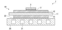
- FIG. 1 shows a power module 1 provided with an insulated circuit board 10 according to the present embodiment.
- the power module 1 is a semiconductor element 3 bonded to an insulating circuit board 10 on which a circuit layer 12 and a metal layer 13 are arranged and one surface (upper surface in FIG. 1) of the circuit layer 12 via a bonding layer 2. And a heat sink 30 arranged on the other side (lower side in FIG. 1) of the metal layer 13.
- the semiconductor element 3 is made of a semiconductor material such as Si.
- the semiconductor element 3 and the circuit layer 12 are bonded via a bonding layer 2.
- the bonding layer 2 is made of, for example, a Sn—Ag-based, Sn—In-based, or Sn—Ag—Cu-based solder material.
- the heat sink 30 is for dissipating heat from the above-mentioned insulating circuit board 10.
- the heat sink 30 is made of copper or a copper alloy, and in this embodiment, it is made of phosphorylated copper.
- the heat sink 30 is provided with a flow path 31 for flowing a cooling fluid.
- the heat sink 30 and the metal layer 13 are joined by a solder layer 32 made of a solder material.
- the solder layer 32 is made of, for example, a Sn—Ag-based, Sn—In-based, or Sn—Ag—Cu-based solder material.
- the insulating circuit board 10 of the present embodiment includes a ceramic substrate 11, a circuit layer 12 disposed on one surface (upper surface in FIG. 1) of the ceramic substrate 11, and ceramics. It includes a metal layer 13 disposed on the other surface (lower surface in FIG. 1) of the substrate 11.
- the ceramic substrate 11 is made of silicon-containing ceramics having excellent insulating properties and heat dissipation, and in this embodiment, it is made of silicon nitride (Si 3 N 4 ).
- the thickness of the ceramic substrate 11 is set, for example, in the range of 0.2 mm or more and 1.5 mm or less, and in the present embodiment, it is set to 0.32 mm.
- the circuit layer 12 is formed by joining a copper plate 22 made of copper or a copper alloy to one surface (upper surface in FIG. 6) of the ceramic substrate 11.
- the circuit layer 12 is formed by joining a copper plate 22 made of a rolled plate of oxygen-free copper to a ceramic substrate 11.
- the thickness of the copper plate 22 to be the circuit layer 12 is set within the range of 0.1 mm or more and 2.0 mm or less, and in this embodiment, it is set to 0.6 mm.
- the metal layer 13 is formed by joining a copper plate 23 made of copper or a copper alloy to the other surface (lower surface in FIG. 6) of the ceramic substrate 11.
- the metal layer 13 is formed by joining a copper plate 23 made of a rolled plate of oxygen-free copper to a ceramic substrate 11.
- the thickness of the copper plate 23 to be the metal layer 13 is set within the range of 0.1 mm or more and 2.0 mm or less, and in this embodiment, it is set to 0.6 mm.
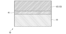
- the active metal compound layer 41 containing the above is formed.
- the active metal compound layer 41 is formed by reacting the active metal contained in the bonding material with the ceramic substrate 11.
- Ti is used as the active metal
- the active metal compound layer 41 is a titanium nitride (TiN) layer.
- the indentation hardness is within the range of 70 mgf / ⁇ m 2 or more and 150 mgf / ⁇ m 2 or less.
- the maximum indentation hardness of the lower limit of the above is 75mgf / ⁇ m 2 or more, and more preferably 85mgf / ⁇ m 2 or more.
- the maximum indentation hardness of the upper limit mentioned is preferably at 135mgf / ⁇ m 2 or less, and more preferably 125mgf / ⁇ m 2 or less.
- the maximum particle size of the active metal compound particles 45 in the active metal compound layer 41 is 180 nm or less.
- the grain boundaries between the active metal compound particles 45 form a metal phase. Since the maximum particle size of the active metal compound particles 45 is 180 nm or less, the proportion of the metal phase having a relatively low hardness increases, and the impact resistance of the active metal compound layer 41 is improved. Thereby, for example, when the terminal material is ultrasonically bonded to the copper member, the generation of cracks in the active metal compound layer 41 is suppressed, the peeling of the copper member and the ceramic member, and the generation of cracks in the ceramic member are suppressed. Can be done.
- the maximum particle size of the active metal compound particles 45 in the active metal compound layer 41 is more preferably 150 nm or less, and even more preferably 120 nm or less.
- the active metal compound layer 41 it is preferable that Si, Cu, and Ag are present in the active metal compound layer 41.
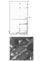
- Si, Cu, and Ag present in the active metal compound layer 41 the interparticles and grain boundaries of the active metal compound particles 45 in the active metal compound layer 41 are observed using a transmission electron microscope to obtain an EDS spectrum. It can be confirmed by obtaining.
- An example of the EDS spectrum of the active metal compound layer 41 is shown in FIG. Peaks of Si, Cu, and Ag have been confirmed, and it can be seen that Si, Cu, and Ag are present in the active metal compound layer 41.
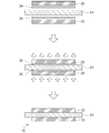
- a ceramic substrate 11 made of silicon nitride (Si 3 N 4 ) is prepared, and as shown in FIG. 6, between the copper plate 22 to be the circuit layer 12 and the ceramic substrate 11, and the copper plate 23 to be the metal layer 13.
- An Ag-Ti-based brazing material (Ag-Cu-Ti-based brazing material) 24 is arranged between the ceramic substrate 11 and the ceramic substrate 11.
- the Ag-Ti-based brazing material (Ag-Cu-Ti-based brazing material) 24 for example, Cu is in the range of 0 mass% or more and 32 mass% or less, and Ti, which is an active metal, is 0.5 mass% or more and 20 mass% or less. It is preferable to use a composition containing Ag and unavoidable impurities in the balance.
- the thickness of the Ag—Cu—Ti brazing material 24 is preferably in the range of 2 ⁇ m or more and 10 ⁇ m or less.
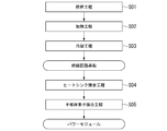
- Heating step S02 Next, while the copper plate 22 and the ceramic substrate 11 are pressurized, they are heated in a heating furnace in a vacuum atmosphere to melt the Ag—Ti brazing material (Ag—Cu—Ti brazing material) 24.
- the heating temperature in the heating step S02 is within the range of the eutectic point temperature of Cu and Si or more and 850 ° C. or less.
- the temperature integral value at the above-mentioned heating temperature is set within the range of 1 ° C. ⁇ h or more and 110 ° C.
- the pressurizing load in this heating step S02 is within the range of 0.029 MPa or more and 2.94 MPa or less.
- the molten Ag—Ti brazing material (Ag—Cu—Ti brazing material) 24 is solidified by cooling.
- the cooling rate in this cooling step S03 is preferably in the range of 2 ° C./min or more and 10 ° C./min or less.
- a eutectic liquid phase is present at the grain boundary of TiN in the active metal compound layer 41, and this eutectic liquid phase is used as a diffusion path for Si and Ag on the ceramic substrate 11 side.
- -Ag, Cu, and Ti of the Cu-Ti brazing material 24 diffuse with each other, and the interfacial reaction of the ceramic substrate 11 is promoted.
- the maximum indentation hardness in the region from 10 ⁇ m to 50 ⁇ m from the bonding interface with the ceramic substrate 11 toward the circuit layer 12 (metal layer 13) is within the range of 70 mgf / ⁇ m 2 or more and 150 mgf / ⁇ m 2 or less.
- the ceramic substrate 11 and the copper plates 22 and 23 are joined by the laminating step S01, the heating step S02, and the cooling step S03, and the insulated circuit board 10 according to the present embodiment is manufactured.
- Heat sink joining step S04 Next, the heat sink 30 is joined to the other surface side of the metal layer 13 of the insulating circuit board 10.
- the insulating circuit board 10 and the heat sink 30 are laminated via a solder material and charged into a heating furnace, and the insulating circuit board 10 and the heat sink 30 are solder-bonded via the solder layer 32.
- semiconductor element joining step S05 Next, the semiconductor element 3 is soldered to one surface of the circuit layer 12 of the insulating circuit board 10.
- the power module 1 shown in FIG. 1 is produced by the above-mentioned steps.
- the circuit layer 12 (metal layer) is formed from the bonding interface between the circuit layer 12 (metal layer 13) and the ceramics substrate 11. Since the maximum pushing hardness in the region from 10 ⁇ m to 50 ⁇ m to 13) is 70 mgf / ⁇ m 2 or more, the copper near the bonding interface is sufficiently melted to form a liquid phase, and the ceramic substrate 11 and the circuit layer are formed. 12 (metal layer 13) is more firmly joined.
- the above-mentioned maximum indentation hardness is suppressed to 150 mgf / ⁇ m 2 or less, the vicinity of the bonding interface is not harder than necessary, and the occurrence of cracks at the time of a thermal cycle load can be suppressed.
- the maximum particle diameter of the active metal compound particles 45 in the active metal compound layer 41 formed at the bonding interface between the ceramic substrate 11 and the circuit layer 12 (metal layer 13) is 180 nm or less.
- the grain boundary region composed of the metal phase having a relatively low hardness occupies a large proportion in the active metal compound layer 41, and the impact resistance in the active metal compound layer 41 can be ensured.
- the terminal material is ultrasonically bonded to the circuit layer 12 (metal layer 13)
- the occurrence of cracks in the active metal compound layer 41 is suppressed, and the circuit layer 12 (metal layer 13) and the ceramic substrate 11 are separated. Further, it is possible to suppress the occurrence of cracks on the ceramic substrate 11.
- the insulating circuit board 10 of the present embodiment when Si, Cu, and Ag are present in the active metal compound layer 41, the occurrence of cracks in the active metal compound layer 41 can be suppressed. At the same time, an unreacted portion is not generated at the bonding interface between the ceramic substrate 11 and the circuit layer 12 (metal layer 13), and the insulating circuit board 10 having higher bonding strength can be obtained.
- a semiconductor element is mounted on an insulating circuit board to form a power module, but the present embodiment is not limited to this.
- an LED element may be mounted on the circuit layer of the insulated circuit board to form an LED module, or a thermoelectric element may be mounted on the circuit layer of the insulated circuit board to form a thermoelectric module.
- the circuit layer and the metal layer are both composed of a copper plate made of copper or a copper alloy, but the present invention is not limited to this.
- the material and joining method of the metal layer are not limited, and the metal layer may not be present, or the metal layer may be aluminum or It may be composed of an aluminum alloy or a laminate of copper and aluminum.
- the material and joining method of the circuit layer are not limited, and the circuit layer may be made of aluminum or an aluminum alloy. , It may be composed of a laminate of copper and aluminum.
- the Ag—Ti brazing material (Ag—Cu—Ti brazing material) 24 is arranged between the copper plates 22 and 23 and the ceramic substrate 11 in the laminating step S01.
- the present invention is not limited to this, and a bonding material containing another active metal may be used.
- the ceramic substrate has been described as being composed of silicon nitride (Si 3 N 4 ), but the present invention is not limited to this, and the ceramic substrate is composed of other silicon-containing ceramics. May be good.
- Example 1 a ceramic substrate (40 mm ⁇ 40 mm ⁇ 0.32 mm) made of silicon nitride (Si 3 N 4) was prepared. A copper plate (37 mm ⁇ 37 mm ⁇ thickness 1.0 mm) made of oxygen-free copper was used on both sides of this ceramic substrate using an Ag—Cu based brazing material containing the active metal shown in Table 1 under the conditions shown in Table 1. An insulating circuit board (copper / ceramics bonded body) was obtained by joining a copper plate and a ceramics substrate. The degree of vacuum of the vacuum furnace at the time of joining was set to 5 ⁇ 10 -3 Pa.
- the maximum indentation hardness was measured in a region from 10 ⁇ m to 50 ⁇ m from the bonding interface between the copper plate and the ceramic substrate to the copper plate side using an indentation hardness tester (ENT-1100a manufactured by Elionix Inc.).
- the target cross section was exposed by buffing to form a measurement surface, and as shown in FIG. 7, the indentation hardness was measured at 50 measurement points at 10 ⁇ m intervals, and the maximum value of the indentation hardness was confirmed. did.
- the load applied in the indenter indentation process and the indentation depth can be continuously measured, and information such as plasticity / elasticity / creep can be obtained from the load-displacement curve. Can be obtained.
- Example 1-8 of the present invention in which the maximum indentation hardness of the bonding interface is within the range of 70 mgf / ⁇ m 2 or more and 150 mgf / ⁇ m 2 or less, the thermal cycle reliability is not limited to the type of active metal. Became " ⁇ ".
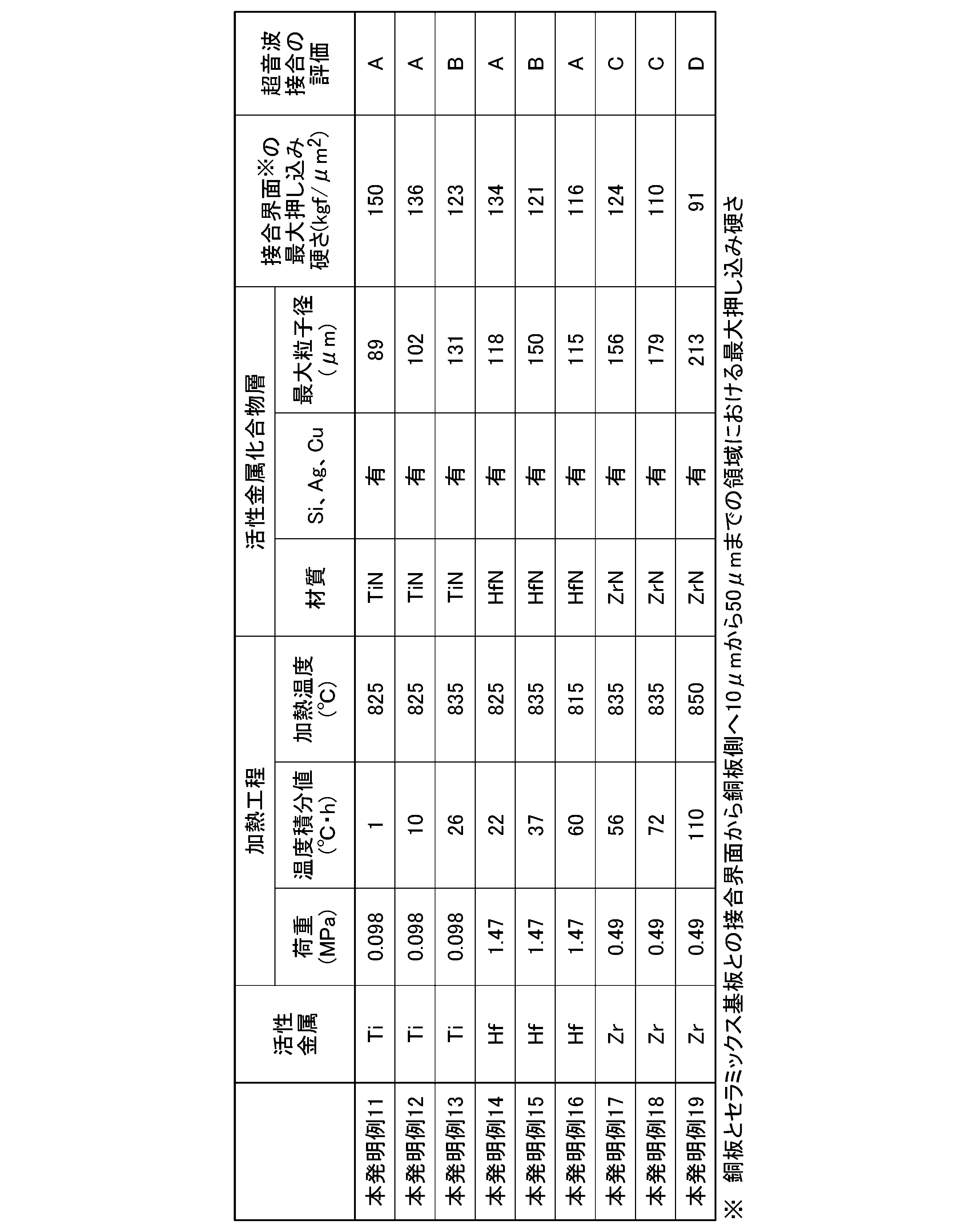
- Example 2 A ceramic substrate (40 mm ⁇ 40 mm ⁇ 0.32 mm) made of silicon nitride (Si 3 N 4) was prepared. A copper plate (37 mm ⁇ 37 mm ⁇ thickness 0.2 mm) made of oxygen-free copper was used on both sides of this ceramic substrate using an Ag—Cu-based brazing material containing the active metal shown in Table 2 under the conditions shown in Table 2. An insulating circuit board (copper / ceramics bonded body) was obtained by joining a copper plate and a ceramics substrate. The degree of vacuum of the vacuum furnace at the time of joining was set to 5 ⁇ 10 -3 Pa.
- the maximum indentation hardness in the vicinity of the joint interface was evaluated by the same method as in Example 1.
- the maximum particle size of the active metal compound particles in the active metal compound layer, the presence or absence of Si, Ag, and Cu in the active metal compound layer, and ultrasonic bonding were evaluated by the methods shown below.
- the active metal compound layer was observed with a transmission electron microscope (Titan ChemiSTEM manufactured by FEI) at a magnification of 500,000 times to obtain a HAADF image.
- the equivalent circle diameter of the active metal compound particles was calculated by image analysis of this HAADF image. From the results of image analysis in 10 fields, the maximum circle-equivalent diameter of the observed active metal compound particles is shown in Table 2 as the maximum particle size.
- Example 11-13 of the present invention in which the active metal is Ti Comparing Example 11-13 of the present invention in which the active metal is Ti, Example 14-16 of the present invention in which the active metal is Hf, and Example 17-19 of the present invention in which the active metal is Zr, the active metal in the active metal compound layer is compared. It is confirmed that by reducing the maximum particle size of the compound particles, it is possible to suppress the peeling of the copper plate and the ceramic substrate during ultrasonic bonding and the occurrence of cracks on the ceramic substrate.
Landscapes
- Engineering & Computer Science (AREA)
- Chemical & Material Sciences (AREA)
- Microelectronics & Electronic Packaging (AREA)
- Mechanical Engineering (AREA)
- Ceramic Engineering (AREA)
- Materials Engineering (AREA)
- Structural Engineering (AREA)
- Organic Chemistry (AREA)
- Manufacturing & Machinery (AREA)
- Inorganic Chemistry (AREA)
- Ceramic Products (AREA)
- Manufacturing Of Printed Wiring (AREA)
Abstract
Description
本願は、2019年12月19日に日本に出願された特願2019-228780号、および2020年11月26日に日本に出願された特願2020-196300号に基づき優先権を主張し、その内容をここに援用する。
例えば、風力発電、電気自動車、ハイブリッド自動車等を制御するために用いられる大電力制御用のパワー半導体素子は、動作時の発熱量が多いことから、これを搭載する基板としては、セラミックス基板と、このセラミックス基板の一方の面に導電性の優れた金属板を接合して形成した回路層と、を備えた絶縁回路基板が、従来から広く用いられている。なお、絶縁回路基板としては、セラミックス基板の他方の面に金属板を接合して金属層を形成したものも提供されている。
また、特許文献2に開示されているように、活性金属ろう付け法によってセラミックス基板と銅板とを接合する場合には、接合温度が900℃と比較的高温とされていることから、やはり、セラミックス基板が劣化してしまうといった問題があった。
このため、従来よりも厳しい冷熱サイクルが負荷される用途であっても、接合強度が高く、かつ、冷熱サイクル負荷時にもセラミックス基板にクラックが生じない絶縁回路基板が求められている。
一方、前述の領域における最大押し込み硬さが150mgf/μm2以下に抑えられているので、接合界面近傍が必要以上に硬くなく、冷熱サイクル負荷時におけるクラックの発生を抑制することができる。
よって、接合強度が高く、かつ、冷熱サイクル信頼性に特に優れた銅/セラミックス接合体を得ることができる。
この場合、前記活性金属化合物層において、相対的に硬度の低い粒界領域(金属相)が占める割合が増加し、前記活性金属化合物層の耐衝撃性が向上する。これにより、例えば、前記銅部材に端子材を超音波接合した時に、前記活性金属化合物層におけるクラックの発生を抑制し、銅部材とセラミックス部材の剥離や、セラミックス部材でのクラックの発生を抑制することができる。
この場合、前記活性金属化合物層内にSi,Cu,Agが存在しているので、前記活性金属化合物層におけるクラックの発生を抑制することができるとともに、前記銅部材と前記セラミックス部材との接合界面に未反応部が生じることが無く、さらに接合強度の高い銅/セラミックス接合体を得ることができる。
一方、前述の領域における最大押し込み硬さが150mgf/μm2以下に抑えられているので、接合界面近傍が必要以上に硬くなく、冷熱サイクル負荷時におけるクラックの発生を抑制することができる。
よって、接合強度が高く、かつ、冷熱サイクル信頼性に特に優れた絶縁回路基板を得ることができる。
この場合、前記活性金属化合物層において、相対的に硬度の低い粒界領域(金属相)が占める割合が増加し、前記活性金属化合物層の耐衝撃性が向上する。これにより、例えば、前記銅板に端子材を超音波接合した時に、前記活性金属化合物層におけるクラックの発生を抑制し、銅板とセラミックス基板の剥離や、セラミックス基板でのクラックの発生を抑制することができる。
この場合、前記活性金属化合物層内にSi,Cu,Agが存在しているので、前記活性金属化合物層におけるクラックの発生を抑制することができるとともに、前記銅板と前記セラミックス基板との接合界面に未反応部が生じることが無く、さらに接合強度の高い絶縁回路基板を得ることができる。
本実施形態に係る銅/セラミックス接合体は、セラミックスからなるセラミックス部材としてのセラミックス基板11と、銅又は銅合金からなる銅部材としての銅板22(回路層12)及び銅板23(金属層13)とが接合されてなる絶縁回路基板10である。図1に、本実施形態である絶縁回路基板10を備えたパワーモジュール1を示す。
接合層2は、例えばSn-Ag系、Sn-In系、若しくはSn-Ag-Cu系のはんだ材で構成されている。
なお、本実施形態においては、ヒートシンク30と金属層13とが、はんだ材からなるはんだ層32によって接合されている。このはんだ層32は、例えばSn-Ag系、Sn-In系、若しくはSn-Ag-Cu系のはんだ材で構成されている。
本実施形態においては、回路層12は、無酸素銅の圧延板からなる銅板22がセラミックス基板11に接合されることで形成されている。
なお、回路層12となる銅板22の厚さは0.1mm以上2.0mm以下の範囲内に設定されており、本実施形態では、0.6mmに設定されている。
本実施形態においては、金属層13は、無酸素銅の圧延板からなる銅板23がセラミックス基板11に接合されることで形成されている。
なお、金属層13となる銅板23の厚さは0.1mm以上2.0mm以下の範囲内に設定されており、本実施形態では、0.6mmに設定されている。
この活性金属化合物層41は、接合材に含まれる活性金属とセラミックス基板11とが反応することによって形成されたものである。
本実施形態では、活性金属としてTiが用いられており、セラミックス基板11が窒化アルミニウムで構成されていることから、活性金属化合物層41は、窒化チタン(TiN)層となる。
なお、上述の最大押し込み硬さの下限は75mgf/μm2以上であることが好ましく、85mgf/μm2以上であることがより好ましい。一方、上述の最大押し込み硬さの上限は135mgf/μm2以下であることが好ましく、125mgf/μm2以下であることがより好ましい。
なお、活性金属化合物層41における活性金属化合物粒子45の最大粒子径は150nm以下であることがさらに好ましく、120nm以下であることがより好ましい。
なお、この活性金属化合物層41に存在するSi,Cu,Agは、活性金属化合物層41における活性金属化合物粒子45の粒子間および粒界を、透過型電子顕微鏡を用いて観察し、EDSスペクトルを得ることによって確認することができる。活性金属化合物層41のEDSスペクトルの一例を図4に示す。Si,Cu,Agのピークが確認されており、活性金属化合物層41内に、Si,Cu,Agが存在していることが分かる。
まず、窒化ケイ素(Si3N4)からなるセラミックス基板11を準備し、図6に示すように、回路層12となる銅板22とセラミックス基板11との間、及び、金属層13となる銅板23とセラミックス基板11との間に、Ag-Ti系ろう材(Ag-Cu-Ti系ろう材)24を配設する。
なお、Ag-Ti系ろう材(Ag-Cu-Ti系ろう材)24としては、例えば、Cuを0mass%以上32mass%以下の範囲内、活性金属であるTiを0.5mass%以上20mass%以下の範囲で含み、残部がAg及び不可避不純物とされた組成のものを用いることが好ましい。また、Ag-Cu-Ti系ろう材24の厚さは、2μm以上10μm以下の範囲内とすることが好ましい。
次に、銅板22とセラミックス基板11とを加圧した状態で、真空雰囲気の加熱炉内で加熱し、Ag-Ti系ろう材(Ag-Cu-Ti系ろう材)24を溶融する。
ここで、加熱工程S02における加熱温度は、CuとSiの共晶点温度以上850℃以下の範囲内とされている。また、この加熱工程S02において、上述の加熱温度における温度積分値は、1℃・h以上110℃・h以下の範囲内とする。
また、この加熱工程S02における加圧荷重は、0.029MPa以上2.94MPa以下の範囲内とする。
そして、加熱工程S02の後、冷却を行うことにより、溶融したAg-Ti系ろう材(Ag-Cu-Ti系ろう材)24を凝固させる。
なお、この冷却工程S03における冷却速度は、2℃/min以上10℃/min以下の範囲内とすることが好ましい。
これにより、セラミックス基板11との接合界面から回路層12(金属層13)側へ10μmから50μmまでの領域における最大押し込み硬さが70mgf/μm2以上150mgf/μm2以下の範囲内となる。
次に、絶縁回路基板10の金属層13の他方の面側にヒートシンク30を接合する。
絶縁回路基板10とヒートシンク30とを、はんだ材を介して積層して加熱炉に装入し、はんだ層32を介して絶縁回路基板10とヒートシンク30とをはんだ接合する。
次に、絶縁回路基板10の回路層12の一方の面に、半導体素子3をはんだ付けにより接合する。
上述の工程により、図1に示すパワーモジュール1が製出される。
一方、上述の最大押し込み硬さが150mgf/μm2以下に抑えられているので、接合界面近傍が必要以上に硬くなく、冷熱サイクル負荷時におけるクラックの発生を抑制することができる。
例えば、本実施形態では、絶縁回路基板に半導体素子を搭載してパワーモジュールを構成するものとして説明したが、これに限定されることはない。例えば、絶縁回路基板の回路層にLED素子を搭載してLEDモジュールを構成してもよいし、絶縁回路基板の回路層に熱電素子を搭載して熱電モジュールを構成してもよい。
例えば、回路層とセラミックス基板とが本発明の銅/セラミックス接合体で構成されていれば、金属層の材質や接合方法に限定はなく、金属層がなくてもよいし、金属層がアルミニウム又はアルミニウム合金で構成されていてもよく、銅とアルミニウムの積層体で構成されていてもよい。
一方、金属層とセラミックス基板とが本発明の銅/セラミックス接合体で構成されていれば、回路層の材質や接合方法に限定はなく、回路層がアルミニウム又はアルミニウム合金で構成されていてもよく、銅とアルミニウムの積層体で構成されていてもよい。
また、本実施形態では、セラミックス基板が窒化ケイ素(Si3N4)で構成されたものとして説明したが、これに限定されることはなく、その他のケイ素含有セラミックスで構成されたものであってもよい。
まず、窒化ケイ素(Si3N4)からなるセラミックス基板(40mm×40mm×0.32mm)を準備した。
このセラミックス基板の両面に、無酸素銅からなる銅板(37mm×37mm×厚さ1.0mm)を、表1に示す活性金属を含むAg-Cu系ろう材を用いて、表1に示す条件で銅板とセラミックス基板とを接合し、絶縁回路基板(銅/セラミックス接合体)を得た。なお、接合時の真空炉の真空度は5×10-3Paとした。
銅板とセラミックス基板との接合界面から銅板側へ10μmから50μmまでの領域において、押し込み硬さ試験機(株式会社エリオニクス製ENT-1100a)を用いて、最大押し込み硬さを測定した。測定条件は、バーコビッチ圧子を用いてFmax=5000mgf(分割数=500、ステップインターバル=20ms)とした。なお、バフ研磨により対象断面を露出させて測定面とし、図7に示すように、10μm間隔で50箇所の測定点において押し込み硬さを測定し、その中での押し込み硬さの最大値を確認した。
この押し込み硬さ試験においては、図8に示すように、圧子押し込み過程で負荷する荷重と押し込み深さを連続的に測定可能であり、荷重-変位曲線から、 塑性/ 弾性/ クリープ等の情報を取得することができる。
以下の雰囲気で保持させた後、SAT検査により、銅板とセラミックス基板の接合界面を検査し、セラミックス割れの有無を判定した。
-78℃×2min←→350℃×2min
そして、割れ発生のサイクル数を評価した。6回未満で割れが確認されたものを「×」、6回以上でも割れが確認されなかったものを「○」と評価した。評価結果を表1に示す。

活性金属としてZrを用いて加熱工程における温度積分値を0.7℃・hとした比較例2においては、接合界面の最大押し込み硬さが160mgf/μm2と本発明の範囲よりも大きくなり、冷熱サイクル信頼性が「×」となった。
窒化ケイ素(Si3N4)からなるセラミックス基板(40mm×40mm×0.32mm)を準備した。
このセラミックス基板の両面に、無酸素銅からなる銅板(37mm×37mm×厚さ0.2mm)を、表2に示す活性金属を含むAg-Cu系ろう材を用いて、表2に示す条件で銅板とセラミックス基板とを接合し、絶縁回路基板(銅/セラミックス接合体)を得た。なお、接合時の真空炉の真空度は5×10-3Paとした。
また、活性金属化合物層における活性金属化合物粒子の最大粒子径、活性金属化合物層中のSi,Ag,Cuの有無、超音波接合について、以下に示す方法で評価した。
活性金属化合物層を透過型電子顕微鏡 (FEI社製 Titan ChemiSTEM)を用いて倍率50万倍で観察し、HAADF像を得た。
このHAADF像の画像解析により、活性金属化合物粒子の円相当径を算出した。10視野における画像解析の結果から、観察された活性金属化合物粒子の最大の円相当径を、最大粒子径として表2に示した。
活性金属化合物層における粒界を透過型電子顕微鏡 (FEI社製 Titan ChemiSTEM)を用いて加速電圧 200kV、倍率50万倍から70万倍、1点あたり7μsで1100フレームを積算した。EDSスペクトルにおいて、Si,Ag,Cuが0.15cps/eVである場合に、Si,Ag,Cuが「有」と評価した。
絶縁回路基板に対して、超音波金属接合機(超音波工業株式会社製:60C-904)を用いて、銅端子(10mm×20mm×2.0mm厚)を、荷重850N,コプラス量0.7mm,接合エリア5mm×5mmの条件で超音波接合した。なお、銅端子はそれぞれ50個ずつ接合した。
接合後に、超音波探傷装置(株式会社日立ソリューションズ製FineSAT200)を用いて、銅板とセラミックス基板の接合界面を検査した。50個中5個以上で銅板とセラミックス基板との剥離又はセラミックス割れが観察されたものを「D」、50個中3個以上4個以下で銅板とセラミックス基板との剥離又はセラミックス割れが観察されたものを「C」、50個中1個以上2個以下で銅板とセラミックス基板との剥離又はセラミックス割れが観察されたものを「B」、50個全てで銅板とセラミックス基板との剥離又はセラミックス割れが観察されなかったものを「A」と評価した。評価結果を表2に示す。
11 セラミックス基板(セラミックス部材)
12 回路層(銅部材)
13 金属層(銅部材)
41 活性金属化合物層
45 活性金属化合物粒子
Claims (6)
- 銅又は銅合金からなる銅部材と、ケイ素含有セラミックスからなるセラミックス部材とが接合されてなる銅/セラミックス接合体であって、
前記銅部材と前記セラミックス部材との接合界面から前記銅部材側へ10μmから50μmまでの領域における最大押し込み硬さが70mgf/μm2以上150mgf/μm2以下の範囲内とされていることを特徴とする銅/セラミックス接合体。 - 前記セラミックス部材と前記銅部材との接合界面においては、前記セラミックス部材側に、Ti,Zr,Nb,Hfから選択される1種又は2種以上の活性金属の化合物を含む活性金属化合物層が形成されており、
前記活性金属化合物層における前記活性金属化合物粒子の最大粒子径が180nm以下であることを特徴とする請求項1に記載の銅/セラミックス接合体。 - 前記活性金属化合物層内に、Si,Cu,Agが存在していることを特徴とする請求項1又は請求項2に記載の銅/セラミックス接合体。
- ケイ素含有セラミックスからなるセラミックス基板の表面に、銅又は銅合金からなる銅板が接合されてなる絶縁回路基板であって、
前記銅板と前記セラミックス基板との接合界面から前記銅板側へ10μmから50μmまでの領域における最大押し込み硬さが70mgf/μm2以上150mgf/μm2以下の範囲内とされていることを特徴とする絶縁回路基板。 - 前記銅板と前記セラミックス基板との接合界面においては、前記セラミックス基板側に、Ti,Zr,Nb,Hfから選択される1種又は2種以上の活性金属の化合物を含む活性金属化合物層が形成されており、
前記活性金属化合物層における前記活性金属化合物粒子の最大粒子径が180nm以下であることを特徴とする請求項4に記載の絶縁回路基板。 - 前記活性金属化合物層内に、Si,Cu,Agが存在していることを特徴とする請求項4又は請求項5に記載の絶縁回路基板。
Priority Applications (4)
| Application Number | Priority Date | Filing Date | Title |
|---|---|---|---|
| EP20902360.5A EP4079711B1 (en) | 2019-12-19 | 2020-12-04 | Copper/ceramic joined body and insulated circuit board |
| CN202080087117.1A CN114845977B (zh) | 2019-12-19 | 2020-12-04 | 铜-陶瓷接合体、及绝缘电路基板 |
| KR1020227023238A KR20220116213A (ko) | 2019-12-19 | 2020-12-04 | 구리/세라믹스 접합체, 및, 절연 회로 기판 |
| US17/786,132 US20230022285A1 (en) | 2019-12-19 | 2020-12-04 | Copper/ceramic joined body and insulated circuit board |
Applications Claiming Priority (4)
| Application Number | Priority Date | Filing Date | Title |
|---|---|---|---|
| JP2019228780 | 2019-12-19 | ||
| JP2019-228780 | 2019-12-19 | ||
| JP2020196300A JP6939973B2 (ja) | 2019-12-19 | 2020-11-26 | 銅/セラミックス接合体、及び、絶縁回路基板 |
| JP2020-196300 | 2020-11-26 |
Publications (1)
| Publication Number | Publication Date |
|---|---|
| WO2021124923A1 true WO2021124923A1 (ja) | 2021-06-24 |
Family
ID=76477312
Family Applications (1)
| Application Number | Title | Priority Date | Filing Date |
|---|---|---|---|
| PCT/JP2020/045199 Ceased WO2021124923A1 (ja) | 2019-12-19 | 2020-12-04 | 銅/セラミックス接合体、及び、絶縁回路基板 |
Country Status (6)
| Country | Link |
|---|---|
| US (1) | US20230022285A1 (ja) |
| EP (1) | EP4079711B1 (ja) |
| KR (1) | KR20220116213A (ja) |
| CN (1) | CN114845977B (ja) |
| TW (1) | TW202142523A (ja) |
| WO (1) | WO2021124923A1 (ja) |
Cited By (4)
| Publication number | Priority date | Publication date | Assignee | Title |
|---|---|---|---|---|
| WO2022224949A1 (ja) * | 2021-04-19 | 2022-10-27 | 三菱マテリアル株式会社 | 銅/セラミックス接合体、および、絶縁回路基板 |
| WO2023286856A1 (ja) * | 2021-07-16 | 2023-01-19 | 三菱マテリアル株式会社 | 銅/セラミックス接合体、および、絶縁回路基板 |
| WO2023286857A1 (ja) * | 2021-07-16 | 2023-01-19 | 三菱マテリアル株式会社 | 銅/セラミックス接合体、および、絶縁回路基板 |
| JP2023013631A (ja) * | 2021-07-16 | 2023-01-26 | 三菱マテリアル株式会社 | 銅/セラミックス接合体、絶縁回路基板、および、銅/セラミックス接合体の製造方法、絶縁回路基板の製造方法 |
Families Citing this family (2)
| Publication number | Priority date | Publication date | Assignee | Title |
|---|---|---|---|---|
| EP4227284A4 (en) * | 2020-10-07 | 2025-09-03 | Toshiba Kk | BONDED BODY, CERAMIC CIRCUIT SUBSTRATE AND SEMICONDUCTOR DEVICE |
| EP4040480A1 (en) * | 2021-02-09 | 2022-08-10 | AT & S Austria Technologie & Systemtechnik Aktiengesellschaft | Electronic device with metallically connected component carrier and fluid cooling member |
Citations (10)
| Publication number | Priority date | Publication date | Assignee | Title |
|---|---|---|---|---|
| JPH04162756A (ja) | 1990-10-26 | 1992-06-08 | Toshiba Corp | 半導体モジュール |
| JP3211856B2 (ja) | 1994-11-02 | 2001-09-25 | 電気化学工業株式会社 | 回路基板 |
| JP2005112677A (ja) * | 2003-10-09 | 2005-04-28 | Hitachi Metals Ltd | セラミックス基板用ろう材及びこれを用いたセラミックス回路基板 |
| JP2009170930A (ja) * | 2009-03-12 | 2009-07-30 | Hitachi Metals Ltd | セラミックス回路基板及びこれを用いたパワー半導体モジュール |
| WO2017213207A1 (ja) * | 2016-06-10 | 2017-12-14 | 田中貴金属工業株式会社 | セラミックス回路基板、及び、セラミックス回路基板の製造方法 |
| JP2018008869A (ja) | 2016-06-30 | 2018-01-18 | 三菱マテリアル株式会社 | 銅/セラミックス接合体、及び、絶縁回路基板 |
| WO2018021472A1 (ja) * | 2016-07-28 | 2018-02-01 | 株式会社 東芝 | 接合体、回路基板、および半導体装置 |
| JP2018140929A (ja) * | 2017-02-28 | 2018-09-13 | 三菱マテリアル株式会社 | 銅/セラミックス接合体、絶縁回路基板、及び、銅/セラミックス接合体の製造方法、絶縁回路基板の製造方法 |
| WO2018221493A1 (ja) * | 2017-05-30 | 2018-12-06 | デンカ株式会社 | セラミックス回路基板及びそれを用いたモジュール |
| JP2020196300A (ja) | 2019-05-31 | 2020-12-10 | 日産自動車株式会社 | 車両のバッテリ搭載構造 |
Family Cites Families (8)
| Publication number | Priority date | Publication date | Assignee | Title |
|---|---|---|---|---|
| JP2539787B2 (ja) * | 1985-11-19 | 1996-10-02 | 住友電気工業株式会社 | 焼結ダイヤモンド工具の製造方法 |
| JP2000183476A (ja) * | 1998-12-14 | 2000-06-30 | Japan Science & Technology Corp | セラミックス回路基板 |
| CN102060556B (zh) * | 2010-11-30 | 2012-11-21 | 哈尔滨工业大学 | 使用Ag-Cu共晶钎料钎焊Ti2AlC陶瓷和铜的方法 |
| JP5899725B2 (ja) * | 2011-09-07 | 2016-04-06 | 三菱マテリアル株式会社 | パワーモジュール用基板、パワーモジュール用基板の製造方法、ヒートシンク付パワーモジュール用基板及びパワーモジュール |
| JP2014172802A (ja) * | 2013-03-12 | 2014-09-22 | Mitsubishi Materials Corp | 銅部材接合用ペースト、接合体、及びパワーモジュール用基板 |
| KR101758586B1 (ko) * | 2014-02-12 | 2017-07-14 | 미쓰비시 마테리알 가부시키가이샤 | 구리/세라믹스 접합체 및 파워 모듈용 기판 |
| KR102516917B1 (ko) * | 2017-04-25 | 2023-03-31 | 덴카 주식회사 | 세라믹스 회로 기판 및 그 제조 방법과 그것을 사용한 모듈 |
| JP7230432B2 (ja) * | 2017-11-02 | 2023-03-01 | 三菱マテリアル株式会社 | 接合体、及び、絶縁回路基板 |
-
2020
- 2020-12-04 EP EP20902360.5A patent/EP4079711B1/en active Active
- 2020-12-04 US US17/786,132 patent/US20230022285A1/en not_active Abandoned
- 2020-12-04 WO PCT/JP2020/045199 patent/WO2021124923A1/ja not_active Ceased
- 2020-12-04 CN CN202080087117.1A patent/CN114845977B/zh active Active
- 2020-12-04 KR KR1020227023238A patent/KR20220116213A/ko not_active Withdrawn
- 2020-12-09 TW TW109143441A patent/TW202142523A/zh unknown
Patent Citations (10)
| Publication number | Priority date | Publication date | Assignee | Title |
|---|---|---|---|---|
| JPH04162756A (ja) | 1990-10-26 | 1992-06-08 | Toshiba Corp | 半導体モジュール |
| JP3211856B2 (ja) | 1994-11-02 | 2001-09-25 | 電気化学工業株式会社 | 回路基板 |
| JP2005112677A (ja) * | 2003-10-09 | 2005-04-28 | Hitachi Metals Ltd | セラミックス基板用ろう材及びこれを用いたセラミックス回路基板 |
| JP2009170930A (ja) * | 2009-03-12 | 2009-07-30 | Hitachi Metals Ltd | セラミックス回路基板及びこれを用いたパワー半導体モジュール |
| WO2017213207A1 (ja) * | 2016-06-10 | 2017-12-14 | 田中貴金属工業株式会社 | セラミックス回路基板、及び、セラミックス回路基板の製造方法 |
| JP2018008869A (ja) | 2016-06-30 | 2018-01-18 | 三菱マテリアル株式会社 | 銅/セラミックス接合体、及び、絶縁回路基板 |
| WO2018021472A1 (ja) * | 2016-07-28 | 2018-02-01 | 株式会社 東芝 | 接合体、回路基板、および半導体装置 |
| JP2018140929A (ja) * | 2017-02-28 | 2018-09-13 | 三菱マテリアル株式会社 | 銅/セラミックス接合体、絶縁回路基板、及び、銅/セラミックス接合体の製造方法、絶縁回路基板の製造方法 |
| WO2018221493A1 (ja) * | 2017-05-30 | 2018-12-06 | デンカ株式会社 | セラミックス回路基板及びそれを用いたモジュール |
| JP2020196300A (ja) | 2019-05-31 | 2020-12-10 | 日産自動車株式会社 | 車両のバッテリ搭載構造 |
Non-Patent Citations (1)
| Title |
|---|
| See also references of EP4079711A4 |
Cited By (9)
| Publication number | Priority date | Publication date | Assignee | Title |
|---|---|---|---|---|
| WO2022224949A1 (ja) * | 2021-04-19 | 2022-10-27 | 三菱マテリアル株式会社 | 銅/セラミックス接合体、および、絶縁回路基板 |
| WO2023286856A1 (ja) * | 2021-07-16 | 2023-01-19 | 三菱マテリアル株式会社 | 銅/セラミックス接合体、および、絶縁回路基板 |
| WO2023286857A1 (ja) * | 2021-07-16 | 2023-01-19 | 三菱マテリアル株式会社 | 銅/セラミックス接合体、および、絶縁回路基板 |
| JP2023013628A (ja) * | 2021-07-16 | 2023-01-26 | 三菱マテリアル株式会社 | 銅/セラミックス接合体、および、絶縁回路基板 |
| JP2023013631A (ja) * | 2021-07-16 | 2023-01-26 | 三菱マテリアル株式会社 | 銅/セラミックス接合体、絶縁回路基板、および、銅/セラミックス接合体の製造方法、絶縁回路基板の製造方法 |
| JP2023013629A (ja) * | 2021-07-16 | 2023-01-26 | 三菱マテリアル株式会社 | 銅/セラミックス接合体、および、絶縁回路基板 |
| JP7739805B2 (ja) | 2021-07-16 | 2025-09-17 | 三菱マテリアル株式会社 | 銅/セラミックス接合体、および、絶縁回路基板 |
| JP7760851B2 (ja) | 2021-07-16 | 2025-10-28 | 三菱マテリアル株式会社 | 銅/セラミックス接合体、および、絶縁回路基板 |
| US12550731B2 (en) | 2021-07-16 | 2026-02-10 | Mitsubishi Materials Corporation | Copper/ceramic assembly, insulating circuit substrate, production method for copper/ceramic assembly, and production method for insulating circuit substrate |
Also Published As
| Publication number | Publication date |
|---|---|
| CN114845977B (zh) | 2023-08-25 |
| EP4079711A1 (en) | 2022-10-26 |
| US20230022285A1 (en) | 2023-01-26 |
| EP4079711A4 (en) | 2024-02-28 |
| TW202142523A (zh) | 2021-11-16 |
| KR20220116213A (ko) | 2022-08-22 |
| CN114845977A (zh) | 2022-08-02 |
| EP4079711B1 (en) | 2026-03-11 |
Similar Documents
| Publication | Publication Date | Title |
|---|---|---|
| KR102459745B1 (ko) | 구리/세라믹스 접합체, 절연 회로 기판, 및, 구리/세라믹스 접합체의 제조 방법, 절연 회로 기판의 제조 방법 | |
| CN114845977B (zh) | 铜-陶瓷接合体、及绝缘电路基板 | |
| JP7056744B2 (ja) | 銅/セラミックス接合体、絶縁回路基板、及び、銅/セラミックス接合体の製造方法、及び、絶縁回路基板の製造方法 | |
| KR101676230B1 (ko) | 접합체 및 파워 모듈용 기판 | |
| JP5991103B2 (ja) | ヒートシンク付パワーモジュール用基板、ヒートシンク付パワーモジュール、及びヒートシンク付パワーモジュール用基板の製造方法 | |
| JP6928297B2 (ja) | 銅/セラミックス接合体、及び、絶縁回路基板 | |
| JP6939973B2 (ja) | 銅/セラミックス接合体、及び、絶縁回路基板 | |
| JP7794558B2 (ja) | 銅/セラミックス接合体、絶縁回路基板、及び、銅/セラミックス接合体の製造方法、絶縁回路基板の製造方法 | |
| KR102524698B1 (ko) | 접합체, 파워 모듈용 기판, 파워 모듈, 접합체의 제조 방법 및 파워 모듈용 기판의 제조 방법 | |
| EP3845511B1 (en) | Copper/ceramic bonded body, insulating circuit board, method for producing copper/ceramic bonded body, and method for manufacturing insulating circuit board | |
| WO2021044844A1 (ja) | 銅/セラミックス接合体、及び、絶縁回路基板 | |
| JP2023086688A (ja) | 銅/セラミックス接合体、および、絶縁回路基板 | |
| JP5828352B2 (ja) | 銅/セラミックス接合体、及び、パワーモジュール用基板 | |
| CN117769533A (zh) | 铜-陶瓷接合体及绝缘电路基板 | |
| CN108701659B (zh) | 接合体、功率模块用基板、功率模块、接合体的制造方法及功率模块用基板的制造方法 | |
| WO2021117327A1 (ja) | 銅/セラミックス接合体、及び、絶縁回路基板 | |
| JP2021017390A (ja) | 銅/セラミックス接合体、絶縁回路基板、及び、銅/セラミックス接合体の製造方法、絶縁回路基板の製造方法 | |
| JP7540345B2 (ja) | 銅/セラミックス接合体、および、絶縁回路基板 | |
| WO2021112046A1 (ja) | 銅/セラミックス接合体、絶縁回路基板、及び、銅/セラミックス接合体の製造方法、絶縁回路基板の製造方法 | |
| CN117897366B (zh) | 铜-陶瓷接合体及绝缘电路基板 | |
| JP2021031315A (ja) | 銅/セラミックス接合体、絶縁回路基板、及び、銅/セラミックス接合体の製造方法、絶縁回路基板の製造方法 | |
| JP2025065004A (ja) | 銅/セラミックス接合体、および、絶縁回路基板 | |
| JP2022165044A (ja) | 銅/セラミックス接合体、および、絶縁回路基板 | |
| CN117222608A (zh) | 铜-陶瓷接合体及绝缘电路基板 |
Legal Events
| Date | Code | Title | Description |
|---|---|---|---|
| 121 | Ep: the epo has been informed by wipo that ep was designated in this application |
Ref document number: 20902360 Country of ref document: EP Kind code of ref document: A1 |
|
| ENP | Entry into the national phase |
Ref document number: 20227023238 Country of ref document: KR Kind code of ref document: A |
|
| NENP | Non-entry into the national phase |
Ref country code: DE |
|
| ENP | Entry into the national phase |
Ref document number: 2020902360 Country of ref document: EP Effective date: 20220719 |
|
| WWG | Wipo information: grant in national office |
Ref document number: 2020902360 Country of ref document: EP |