WO2021129752A1 - 一种环形布局的模块化并联半桥集成组件 - Google Patents
一种环形布局的模块化并联半桥集成组件 Download PDFInfo
- Publication number
- WO2021129752A1 WO2021129752A1 PCT/CN2020/139072 CN2020139072W WO2021129752A1 WO 2021129752 A1 WO2021129752 A1 WO 2021129752A1 CN 2020139072 W CN2020139072 W CN 2020139072W WO 2021129752 A1 WO2021129752 A1 WO 2021129752A1
- Authority
- WO
- WIPO (PCT)
- Prior art keywords
- electrically connected
- bridge
- inductor
- insulated gate
- pin
- Prior art date
- Legal status (The legal status is an assumption and is not a legal conclusion. Google has not performed a legal analysis and makes no representation as to the accuracy of the status listed.)
- Ceased
Links
Images




Classifications
-
- H—ELECTRICITY
- H02—GENERATION; CONVERSION OR DISTRIBUTION OF ELECTRIC POWER
- H02M—APPARATUS FOR CONVERSION BETWEEN AC AND AC, BETWEEN AC AND DC, OR BETWEEN DC AND DC, AND FOR USE WITH MAINS OR SIMILAR POWER SUPPLY SYSTEMS; CONVERSION OF DC OR AC INPUT POWER INTO SURGE OUTPUT POWER; CONTROL OR REGULATION THEREOF
- H02M7/00—Conversion of AC power input into DC power output; Conversion of DC power input into AC power output
- H02M7/003—Constructional details, e.g. physical layout, assembly, wiring or busbar connections
-
- H—ELECTRICITY
- H02—GENERATION; CONVERSION OR DISTRIBUTION OF ELECTRIC POWER
- H02M—APPARATUS FOR CONVERSION BETWEEN AC AND AC, BETWEEN AC AND DC, OR BETWEEN DC AND DC, AND FOR USE WITH MAINS OR SIMILAR POWER SUPPLY SYSTEMS; CONVERSION OF DC OR AC INPUT POWER INTO SURGE OUTPUT POWER; CONTROL OR REGULATION THEREOF
- H02M7/00—Conversion of AC power input into DC power output; Conversion of DC power input into AC power output
- H02M7/42—Conversion of DC power input into AC power output without possibility of reversal
- H02M7/44—Conversion of DC power input into AC power output without possibility of reversal by static converters
- H02M7/48—Conversion of DC power input into AC power output without possibility of reversal by static converters using discharge tubes with control electrode or semiconductor devices with control electrode
- H02M7/53—Conversion of DC power input into AC power output without possibility of reversal by static converters using discharge tubes with control electrode or semiconductor devices with control electrode using devices of a triode or transistor type requiring continuous application of a control signal
- H02M7/537—Conversion of DC power input into AC power output without possibility of reversal by static converters using discharge tubes with control electrode or semiconductor devices with control electrode using devices of a triode or transistor type requiring continuous application of a control signal using semiconductor devices only, e.g. single switched pulse inverters
- H02M7/5387—Conversion of DC power input into AC power output without possibility of reversal by static converters using discharge tubes with control electrode or semiconductor devices with control electrode using devices of a triode or transistor type requiring continuous application of a control signal using semiconductor devices only, e.g. single switched pulse inverters in a bridge configuration
-
- H—ELECTRICITY
- H10—SEMICONDUCTOR DEVICES; ELECTRIC SOLID-STATE DEVICES NOT OTHERWISE PROVIDED FOR
- H10W—GENERIC PACKAGES, INTERCONNECTIONS, CONNECTORS OR OTHER CONSTRUCTIONAL DETAILS OF DEVICES COVERED BY CLASS H10
- H10W40/00—Arrangements for thermal protection or thermal control
- H10W40/20—Arrangements for cooling
- H10W40/22—Arrangements for cooling characterised by their shape, e.g. having conical or cylindrical projections
-
- H—ELECTRICITY
- H02—GENERATION; CONVERSION OR DISTRIBUTION OF ELECTRIC POWER
- H02M—APPARATUS FOR CONVERSION BETWEEN AC AND AC, BETWEEN AC AND DC, OR BETWEEN DC AND DC, AND FOR USE WITH MAINS OR SIMILAR POWER SUPPLY SYSTEMS; CONVERSION OF DC OR AC INPUT POWER INTO SURGE OUTPUT POWER; CONTROL OR REGULATION THEREOF
- H02M1/00—Details of apparatus for conversion
- H02M1/08—Circuits specially adapted for the generation of control voltages for semiconductor devices incorporated in static converters
- H02M1/088—Circuits specially adapted for the generation of control voltages for semiconductor devices incorporated in static converters for the simultaneous control of series or parallel connected semiconductor devices
-
- H—ELECTRICITY
- H05—ELECTRIC TECHNIQUES NOT OTHERWISE PROVIDED FOR
- H05K—PRINTED CIRCUITS; CASINGS OR CONSTRUCTIONAL DETAILS OF ELECTRIC APPARATUS; MANUFACTURE OF ASSEMBLAGES OF ELECTRICAL COMPONENTS
- H05K1/00—Printed circuits
- H05K1/18—Printed circuits structurally associated with non-printed electric components
- H05K1/181—Printed circuits structurally associated with non-printed electric components associated with surface mounted components
Definitions
- the present invention relates to the technical field of power semiconductors, in particular to a modular parallel half-bridge integrated assembly with a ring layout.
- IGBT modules are modular semiconductor products that are packaged by insulated gate bipolar transistor chips and freewheeling diode chips through specific circuit bridges; the packaged IGBT modules are directly used in inverters, UPS uninterruptible power supplies and other equipment .
- the crimping type IGBT devices on the existing market are all single-tube devices.
- the distance between the capacitor terminals and the two ends of the IGBT is relatively long.
- There is still a large parasitic inductance inevitably, resulting in a large overvoltage when the IGBT device is turned off, which poses a threat to the application of the device, and it is difficult to further increase the device capacity.
- the parasitic inductance and the capacitor will form a series resonant circuit, which will make the actual capacitor resonate at a certain frequency. This phenomenon is called self-resonance of the capacitor.
- Stray inductance and adopt a snubber circuit with appropriate structural parameters to suppress and absorb overvoltage.
- the present invention proposes a modular parallel half-bridge integrated component with a ring layout, which solves the problems of large commutation loop parasitic inductance of the existing parallel half-bridge integrated component and unbalanced currents of various sub-modules.
- the sub-modules are composed of upper half-bridge insulated gate bipolar transistors and lower half-bridge insulated gate bipolar transistors. It consists of a transistor and a DC capacitor, characterized in that the anode of the capacitor C4 is electrically connected to the first pin of the inductor L7, and the second pin of the inductor L7 is electrically connected to the DC anode of the insulated gate bipolar transistor T7.
- the DC negative pole of the insulated gate bipolar transistor T7 is electrically connected to the first pin of the inductor L8, the second pin of the inductor L8 is electrically connected to the electrical node P2, and the first pin of the inductor L8 is electrically connected to the insulated gate bipolar
- the DC positive pole of the insulated gate bipolar transistor T8, the DC negative pole of the insulated gate bipolar transistor T8 is electrically connected to the negative pole of the capacitor C4; the positive pole of the capacitor C5 is electrically connected to the first pin of the inductor L9, and the first pin of the inductor L9
- the two pins are electrically connected to the DC positive pole of the insulated gate bipolar transistor T9, the DC negative pole of the insulated gate bipolar transistor T9 is electrically connected to the first pin of the inductor L10, and the second pin of the inductor L10 is electrically connected to the The second pin of the inductor L8, the first pin of the inductor L10 is electrically connected to the DC anode
- the DC negative electrode is electrically connected to the first pin of the inductor L12
- the second pin of the inductor L12 is electrically connected to the first pin of the inductor L10
- the first pin of the inductor L12 is electrically connected to an insulated gate bipolar transistor
- the direct current positive electrode of T12, and the direct current negative electrode of the insulated gate bipolar transistor T12 are electrically connected to the negative electrode of the capacitor C6.
- the electrical connection terminals of the submodule include a DC positive pole, a DC negative pole, an AC terminal, an upper half bridge grid, an upper half bridge emitter, a lower half bridge grid, and a lower half bridge emitter.
- the upper half-bridge insulated gate bipolar transistor and the lower half-bridge insulated gate bipolar transistor are respectively composed of a plurality of half-bridge insulated gate bipolar transistors connected in parallel.
- the heat dissipation surface of the half-bridge insulated gate bipolar transistor is connected to a heat sink.
- the assembly composed of the sub-modules and the heat sink presents a circular layout to achieve structural symmetry.
- a driving board is arranged inside the ring formed by a plurality of the sub-modules, and the driving board is respectively connected with the upper half-bridge gate, upper half-bridge emitter, lower half-bridge gate, and lower half-bridge emitter of each sub-module. Extremely electrical connection.
- the DC positive pole of the submodule is electrically connected to the positive DC terminal of the collection busbar.
- the DC negative pole of the sub-module is electrically connected to the negative DC terminal of the collection busbar.
- the AC terminal of the sub-module is electrically connected to the AC terminal of the collective busbar.
- the modular parallel half-bridge integrated component of the circular layout is connected in parallel through the circular layout of several sub-modules to ensure that the parasitic inductance of the commutation loop and the parasitic inductance of the AC loop are the same, thereby realizing uniform current of the sub-modules and convenient
- the capacity of the components is further improved.
- the switching speed of the component is faster, and the voltage stress is small at the same time, which greatly improves its application reliability.
- Fig. 1 is a schematic diagram of a traditional centralized layout circuit of a modular parallel half-bridge integrated assembly with a circular layout according to an embodiment of the present invention, where T1 to T6 represent insulated gate bipolar transistors, and D1 to D6 represent diodes. C1 ⁇ C3 represent capacitors, and P1 is an electrical node;
- Fig. 2 is a circuit schematic diagram of a modular parallel half-bridge integrated assembly with a circular layout according to an embodiment of the present invention, in which T7 ⁇ T12 represent insulated gate bipolar transistors, D7 ⁇ D12 represent diodes, and C4 ⁇ C6 represent Capacitor, P2 is the electrical node;
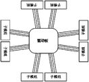
- Fig. 3 is a schematic top view of a modular parallel half-bridge integrated assembly with a circular layout according to an embodiment of the present invention
- FIG. 4 is a circuit diagram of a sub-module of a modular parallel half-bridge integrated assembly in a circular layout according to an embodiment of the present invention
- FIG. 5 is a schematic diagram of the connection structure between the sub-modules and the driving board of a modular parallel half-bridge integrated assembly in a circular layout according to an embodiment of the present invention
- FIG. 6 is a schematic diagram of the AC terminal connection structure of the sub-modules of a modular parallel half-bridge integrated assembly in a circular layout according to an embodiment of the present invention
- FIG. 7 is a schematic diagram of the connection structure of the positive DC collecting bus bar and the negative DC collecting bus bar of the sub-modules of the modular parallel half-bridge integrated assembly in a circular layout according to an embodiment of the present invention.
- a modular parallel half-bridge integrated assembly with a circular layout includes capacitors C4, C5, C6 and sub-modules.
- the sub-modules are composed of upper half-bridge insulated gates. It consists of a bipolar transistor, a lower half-bridge insulated gate bipolar transistor, and a DC capacitor, characterized in that the anode of the capacitor C4 is electrically connected to the first pin of the inductor L7, and the second pin of the inductor L7 is electrically connected The DC positive pole of the insulated gate bipolar transistor T7, the DC negative pole of the insulated gate bipolar transistor T7 is electrically connected to the first pin of the inductor L8, and the second pin of the inductor L8 is electrically connected to the electrical node P2.
- the first pin of the inductor L8 is electrically connected to the DC anode of the insulated gate bipolar transistor T8, the DC cathode of the insulated gate bipolar transistor T8 is electrically connected to the cathode of the capacitor C4; the anode of the capacitor C5 is electrically connected to the inductor
- the first pin of L9, the second pin of the inductor L9 is electrically connected to the DC anode of the insulated gate bipolar transistor T9, and the DC cathode of the insulated gate bipolar transistor T9 is electrically connected to the first pin of the inductor L10
- the second pin of the inductor L10 is electrically connected to the second pin of the inductor L8, the first pin of the inductor L10 is electrically connected to the DC positive electrode of the insulated gate bipolar transistor T10, and the insulated gate bipolar transistor T10
- the DC negative pole of the transistor T10 is electrically connected to the negative pole of the capacitor C5; the positive pole of the capacitor C6 is electrical
- the DC positive pole, the DC negative pole of the insulated gate bipolar transistor T11 is electrically connected to the first pin of the inductor L12
- the second pin of the inductor L12 is electrically connected to the first pin of the inductor L10
- the inductor L12 The first pin of is electrically connected to the DC positive electrode of the insulated gate bipolar transistor T12
- the DC negative electrode of the insulated gate bipolar transistor T12 is electrically connected to the negative electrode of the capacitor C6.
- the electrical connection terminals of the sub-modules include DC positive, DC negative, AC terminals, upper half-bridge grid, upper half-bridge emitter, lower half-bridge grid, and lower Half-bridge emitter.
- the upper half-bridge insulated gate bipolar transistor and the lower half-bridge insulated gate bipolar transistor are respectively composed of several half-bridge insulated gate bipolar transistors in parallel.
- the heat dissipation surface of the half-bridge insulated gate bipolar transistor is connected to a heat sink.
- the combined body composed of the sub-modules and the heat sink presents a circular layout to achieve structural symmetry.
- a driving board is arranged inside the ring formed by several sub-modules, and the driving board is respectively connected to the upper half-bridge gate, upper half-bridge emitter, and upper half-bridge emitter of each sub-module.
- the gate of the lower half bridge and the emitter of the lower half bridge are electrically connected.
- the DC positive pole of the submodule is electrically connected to the positive DC terminal of the collecting busbar.
- the DC negative pole of the submodule is electrically connected to the negative DC terminal of the collecting busbar.
- the AC terminal of the sub-module is electrically connected to the AC terminal of the collecting busbar.
- the modular parallel half-bridge integrated component with a circular layout adopts a symmetrical or circular layout, resulting in the same parasitic inductance of the commutation loop and the parasitic inductance of the AC loop in each sub-module. It is the main factor that causes the sub-module current balance.
- the same inductance means the same sub-module current; at the same time, the size of the parasitic inductance is directly determined by the length of the loop. Due to the small size of each IGBT device and capacitor, the commutation loop is closely integrated.
- the parasitic inductance is small, resulting in a small overshoot of the device voltage and a faster switching speed; the quadrilateral layout of each sub-module ensures that the parasitic inductance of the commutation loop and the parasitic inductance of the AC loop are the same, and the current balance of each sub-module is realized.
- this integrated component is composed of 8 sub-modules in parallel.
- the half-bridge integrated component includes 4 sub-modules, 4 radiators, and 1 drive board. , Negative DC, collecting busbars, and AC collecting busbars are connected together; the sub-module is composed of upper half-bridge IGBT devices, lower half-bridge IGBT devices, DC capacitors, and other auxiliary components; upper and lower half-bridge IGBT devices They are composed of several IGBT devices in parallel.
- the sub-module includes 7 electrical connection terminals, which are DC positive, DC negative, AC terminal, upper half bridge grid, upper half bridge emitter, lower half bridge grid, and lower half bridge emitter. ;
- the radiator is used in conjunction with the sub-module and connected to the heat dissipation surface of each IGBT device of the sub-module.
- the radiator takes away heat through water or air cooling; the combination of the sub-module and the radiator presents a quadrilateral layout to achieve The symmetry of the structure.
- the driving board is respectively connected with the upper half bridge gate, upper half bridge emitter, lower half bridge gate, and lower half bridge emitter of each sub-module.
- the positive DC collection busbars are respectively connected to the DC anodes of each sub-module, showing a quadrilateral structure; the negative DC collection busbars are respectively connected with the DC negatives of each sub-module, showing a quadrilateral structure.
Landscapes
- Engineering & Computer Science (AREA)
- Power Engineering (AREA)
- Inverter Devices (AREA)
- Power Conversion In General (AREA)
Abstract
本发明公开了一种环形布局的模块化并联半桥集成组件,该组件由若干个子模组并联组成,以提升组件的电流容量,各个子模组环形布局并联连接,实现各个子模组的电流平衡。半桥集成组件包括若干个子模组、若干个散热器、驱动板、正极直流汇集母排、负极直流汇集母排、交流汇集母排。本发明由于各个绝缘栅双极型晶体管IGBT器件与电容紧密结合,换流回路寄生电感较小,导致器件电压过冲较小、开关速度较快,实现各个子模组电流均衡。
Description
本发明涉及功率半导体技术领域,具体来说,涉及一种环形布局的模块化并联半桥集成组件。
20世纪80年代以来,随着电力电子技术的飞速发展,各种电力电子装置在工业中的应用越来越广泛。随着需求的增加,电力电子装置趋于大容量、高功率密度,开关器件的电压、电流等级也随之增大。以现在广泛使用的绝缘栅双极型晶体管(insulated gate bipolar transistor,IGBT)为例,1700~6500V,2000~3600A的大功率IGBT模块已得到广泛的使用,压接型封装的IGBT器件凭借其容量大、结构紧凑、双面散热、失效短路模式等优点,已成为一种适用于电力系统高压大功率电力电子器件。
IGBT模组是由绝缘栅双极型晶体管芯片与续流二极管芯片通过特定的电路桥接封装而成的模块化半导体产品;封装后的IGBT模组直接应用于变频器、UPS不间断电源等设备上。
目前,现有市场上的压接型IGBT器件都是单管器件,在构成半桥电路时,即使组件结构设计的足够紧凑,由于电容及IGBT尺寸较大,电容端子与IGBT两端距离较远,仍不可避免存在较大的寄生电感,导致IGBT器件在关断时仍存在较大过电压,对器件应用造成威胁,同时装置容量也很难进一步得到提升。
寄生电感会与电容构成串联谐振回路,会使实际的电容在某个频率上发生谐振,这种现象称为电容的自谐振,另外,为了抑制开关管的电压尖峰,需要尽可能的减小线路杂散电感,并且采用适当结构参数的缓冲电路来抑制和吸收过电压。
发明内容
针对相关技术中的问题,本发明提出一种环形布局的模块化并联半桥集成组件,解决现有并联半桥集成组件的换流回路寄生电感较大、各个子模组电流不均衡的问题。
为了实现上述技术目的,本发明的技术方案是这样的:
设计一种环形布局的模块化并联半桥集成组件,包括电容C4、C5、C6和子模组,所述子模组是由上半桥绝缘栅双极型晶体管、下半桥绝缘栅双极型晶体管、直流电容组成,其特征在于,所述电容C4的正极电连接电感L7的第一引脚,所述电感L7的第二引脚电连接绝缘栅双极型晶体管T7的直流正极,所述绝缘栅双极型晶体管T7的直流负极电连接电感L8的第一引脚,所述电感L8的第二引脚电连接电气节点P2,所述电感L8的第一引脚电连接绝缘栅双极型晶体管T8的直流正极,所述绝缘栅双极型晶体管T8的直流负极电连接所述电容C4的负极;所述电容C5的正极电连接电感L9的第一引脚,所述电感L9的第二引脚电连接绝缘栅双极型晶体管T9的直流正极,所述绝缘栅双极型晶体管T9的直流负极电连接电感L10的第一引脚,所述电感L10的第二引脚电连接所述电感L8的第二引脚,所述电感L10的第一引脚电连接绝缘栅双极型晶体管T10的直流正极,所述绝缘栅双极型晶体管T10的直流负极电连接所述电容C5的负极;所述电容C6的正极电连接电感L11的第一引脚,所述电感L11的第二引脚电连接绝缘栅双极型晶体管T11的直流正极,所述绝缘栅双极型晶体管T11的直流负极电连接电感L12的第一引脚,所述电感L12的第二引脚电连接所述电感L10的第一引脚,所述电感L12的第一引脚电连接绝缘栅双极型晶体管T12的直流正极,所述绝缘栅双极型晶体管T12的直流负极电连接所述电容C6的负极。
进一步,所述子模组的电气接线端子包含直流正极、直流负极、交流端、上半桥栅极、上半桥发射极、下半桥栅极、下半桥发射极。
进一步,所述上半桥绝缘栅双极型晶体管、下半桥绝缘栅双极型晶体管分别由若干个半桥绝缘栅双极型晶体管并联组成。
进一步,所述半桥绝缘栅双极型晶体管的散热面连接散热器。
进一步,所述的子模组、散热器构成的组合体呈现环形布局,实现结构的对称。
进一步,若干所述子模组构成的环形内部设置有驱动板,所述驱动板分别与各个子模组的上半桥栅极、上半桥发射极、下半桥栅极、下半桥发射极电连接。
进一步,所述子模组的直流正极电连接汇集母排的正极直流端。
进一步,所述子模组的直流负极电连接汇集母排的负极直流端。
进一步,所述子模组的交流端电连接汇集母排的交流端。
本发明的有益效果:这种环形布局的模块化并联半桥集成组件,通过若干个子模组环形布局并联,保证换流回路寄生电感以及交流回路寄生电感相同,从而实现子模组电流均匀,便于组件的容量进一步提升。同时由于每个子模组结构紧凑,换流回路寄生电感较小,使得组件开关速度较快,同时电压应力较小,大幅提高其应用可靠性。
为了更清楚地说明本发明实施例或现有技术中的技术方案,下面将对实施例中所需要使用的附图作简单地介绍,显而易见地,下面描述中的附图仅仅是本发明的一些实施例,对于本领域普通技术人员来讲,在不付出创造性劳动的前提下,还可以根据这些附图获得其他的附图。
图1是根据本发明实施例所述一种环形布局的模块化并联半桥集成组件的传统集中式布局电路原理图,其中,T1~T6代表绝缘栅双极型晶体管,D1~D6代表二极管,C1~C3代表电容器,P1为电气节点;
图2是根据本发明实施例所述一种环形布局的模块化并联半桥集成组件的电路原理图,其中,T7~T12代表绝缘栅双极型晶体管,D7~D12代表二极管,C4~C6代表电容器,P2为电气节点;
图3是根据本发明实施例所述一种环形布局的模块化并联半桥集成组件的俯视结构示意图;
图4是根据本发明实施例所述一种环形布局的模块化并联半桥集成组件的子模组的电路图;
图5是根据本发明实施例所述一种环形布局的模块化并联半桥集成组件的子模组与驱动板连接结构示意图;
图6是根据本发明实施例所述一种环形布局的模块化并联半桥集成组件的子模组交流端连接结构示意图;
图7是根据本发明实施例所述一种环形布局的模块化并联半桥集成组件的子模组正极直流汇集母排、负极直流汇集母排连接结构示意图。
下面将结合本发明实施例中的附图,对本发明实施例中的技术方案进行清楚、完整地描述,显然,所描述的实施例仅仅是本发明一部分实施例,而不是全部的实施例。基于本发明中的实施例,本领域普通技术人员所获得的所有其他实施例,都属于本发明保护的范围。
如图2所示,根据本发明实施例所述的一种环形布局的模块化并联半桥集成组件,包括电容C4、C5、C6和子模组,所述子模组是由上半桥绝缘栅双极型晶体管、下半桥绝缘栅双极型晶体管、直流电容组成,其特征在于,所述电容C4的正极电连接电感L7的第一引脚,所述电感L7的第二引脚电连接绝缘栅双极型晶体管T7的直流正极,所述绝缘栅双极型晶体管T7的直流负极电连接电感L8的第一引脚,所述电感L8的第二引脚电连接电气节点P2,所述电感L8的第一引脚电连接绝缘栅双极型晶体管T8的直流正极,所述绝缘栅双极型晶体管T8的直流负极电连接所述电容C4的负极;所述电容C5的正极电连接电感L9的第一引脚,所述电感L9的第二引脚电连接绝缘栅双极型晶体管T9的直流正极,所述绝缘栅双极型晶体管T9的直流负极电连接电感L10的第一引脚,所述电感L10的第二引脚电连接所述电感L8的第二引脚,所述电感L10的第一引脚电连接绝缘栅双极型晶体管T10的直流正极,所述绝缘栅双极型晶体管T10的直流负极电连接所述电容C5的负极;所述电容C6的正极电连接电感L11的第一引脚,所述电感L11的第二引脚 电连接绝缘栅双极型晶体管T11的直流正极,所述绝缘栅双极型晶体管T11的直流负极电连接电感L12的第一引脚,所述电感L12的第二引脚电连接所述电感L10的第一引脚,所述电感L12的第一引脚电连接绝缘栅双极型晶体管T12的直流正极,所述绝缘栅双极型晶体管T12的直流负极电连接所述电容C6的负极。
如图4所示,在本实施例中,所述子模组的电气接线端子包含直流正极、直流负极、交流端、上半桥栅极、上半桥发射极、下半桥栅极、下半桥发射极。
如图1-4所示,在本实施例中,所述上半桥绝缘栅双极型晶体管、下半桥绝缘栅双极型晶体管分别由若干个半桥绝缘栅双极型晶体管并联组成。
如图3所示,在本实施例中,所述半桥绝缘栅双极型晶体管的散热面连接散热器。
如图3所示,在本实施例中,所述的子模组、散热器构成的组合体呈现环形布局,实现结构的对称。
如图5所示,在本实施例中,若干所述子模组构成的环形内部设置有驱动板,所述驱动板分别与各个子模组的上半桥栅极、上半桥发射极、下半桥栅极、下半桥发射极电连接。
如图7所示,在本实施例中,所述子模组的直流正极电连接汇集母排的正极直流端。
如图7所示,在本实施例中,所述子模组的直流负极电连接汇集母排的负极直流端。
如图6所示,在本实施例中,所述子模组的交流端电连接汇集母排的交流端。
为方便对上述技术方案的进一步理解,现对其结构原理进行说明:
如图1-7所示,这种环形布局的模块化并联半桥集成组件,采用对称式或环形布局方式,导致各个子模组内部的换流回路寄生电感以及交流回路寄生电感相同,寄生电感是造成子模块电流均衡的主要因素,电感相同意味着 子模块电流相同;与此同时,寄生电感大小由回路长短直接决定,由于各个IGBT器件与电容尺寸较小,通过紧密结合设计,换流回路寄生电感较小,导致器件电压过冲较小、开关速度较快;各个子模组通过四边形布局,保证换流回路寄生电感以及交流回路寄生电感相同,实现各个子模组电流均衡。
如图3所示,这种集成组件采用8个子模组并联组成,其改进之处在于,该半桥集成组件包括4个子模组、4个散热器、1个驱动板,各部分通过正极直流、负极直流、汇集母排、交流汇集母排连接在一起;子模组是由上半桥IGBT器件、下半桥IGBT器件、直流电容、其他辅助元器件组接而成;上下半桥IGBT器件都是由若干个IGBT器件并联组成。
如图4所示,子模组包括7个电气接线端子,分别为直流正极、直流负极、交流端、上半桥栅极、上半桥发射极、下半桥栅极、下半桥发射极;将散热器与子模组配合使用,与子模组各个IGBT器件的散热面连接,散热器通过水冷或者风冷带走热量;子模组与散热器构成的组合体,呈现四边形布局,实现结构的对称。
如图5所示,驱动板分别与各个子模组的上半桥栅极、上半桥发射极、下半桥栅极、下半桥发射极相连接。
如图7所示,正极直流汇集母排分别与各个子模组的直流正极相连接,呈现四边形结构;负极直流汇集母排分别与各个子模组的直流负极相连接,呈现四边形结构。
以上仅为本发明的较佳实施例而已,并不用以限制本发明,凡在本发明的精神和原则之内,所作的任何修改、等同替换、改进等,均应包含在本发明的保护范围之内。
Claims (9)
- 一种环形布局的模块化并联半桥集成组件,包括电容C4、C5、C6和子模组,所述子模组包含有上半桥绝缘栅双极型晶体管、下半桥绝缘栅双极型晶体管、直流电容,其特征在于,所述电容C4的正极电连接电感L7的第一引脚,所述电感L7的第二引脚电连接绝缘栅双极型晶体管T7的直流正极,所述绝缘栅双极型晶体管T7的直流负极电连接电感L8的第一引脚,所述电感L8的第二引脚电连接电气节点P2,所述电感L8的第一引脚电连接绝缘栅双极型晶体管T8的直流正极,所述绝缘栅双极型晶体管T8的直流负极电连接所述电容C4的负极;所述电容C5的正极电连接电感L9的第一引脚,所述电感L9的第二引脚电连接绝缘栅双极型晶体管T9的直流正极,所述绝缘栅双极型晶体管T9的直流负极电连接电感L10的第一引脚,所述电感L10的第二引脚电连接所述电感L8的第二引脚,所述电感L10的第一引脚电连接绝缘栅双极型晶体管T10的直流正极,所述绝缘栅双极型晶体管T10的直流负极电连接所述电容C5的负极;所述电容C6的正极电连接电感L11的第一引脚,所述电感L11的第二引脚电连接绝缘栅双极型晶体管T11的直流正极,所述绝缘栅双极型晶体管T11的直流负极电连接电感L12的第一引脚,所述电感L12的第二引脚电连接所述电感L10的第一引脚,所述电感L12的第一引脚电连接绝缘栅双极型晶体管T12的直流正极,所述绝缘栅双极型晶体管T12的直流负极电连接所述电容C6的负极。
- 根据权利要求1所述的一种环形布局的模块化并联半桥集成组件,其特征在于,所述子模组的电气接线端子包含有直流正极、直流负极、交流端、上半桥栅极、上半桥发射极、下半桥栅极、下半桥发射极。
- 根据权利要求1所述的一种环形布局的模块化并联半桥集成组件,其特征在于,所述上半桥绝缘栅双极型晶体管、下半桥绝缘栅双极型晶体管分别由若干个半桥绝缘栅双极型晶体管并联组成。
- 根据权利要求1所述的一种环形布局的模块化并联半桥集成组件,其特征在于,所述半桥绝缘栅双极型晶体管的散热面连接散热器。
- 根据权利要求4所述的一种环形布局的模块化并联半桥集成组件,其特征在于,所述的子模组、散热器构成的组合体呈现环形布局,所述组合体实现结构的对称。
- 根据权利要求1所述的一种环形布局的模块化并联半桥集成组件, 其特征在于,若干所述子模组构成的环形内部设置有驱动板,所述驱动板分别与各个子模组的上半桥栅极、上半桥发射极、下半桥栅极、下半桥发射极电连接。
- 根据权利要求1所述的一种环形布局的模块化并联半桥集成组件,其特征在于,所述子模组的直流正极电连接汇集母排的正极直流端。
- 根据权利要求1所述的一种环形布局的模块化并联半桥集成组件,其特征在于,所述子模组的直流负极电连接汇集母排的负极直流端。
- 根据权利要求1所述的一种环形布局的模块化并联半桥集成组件,其特征在于,所述子模组的交流端电连接汇集母排的交流端。
Priority Applications (2)
| Application Number | Priority Date | Filing Date | Title |
|---|---|---|---|
| EP20905313.1A EP4068609A4 (en) | 2019-12-24 | 2020-12-24 | MODULAR PARALLEL INTEGRATED HALF-BRIDGE ARRANGEMENT WITH ANNULAR ARRANGEMENT |
| US17/844,748 US12003188B2 (en) | 2019-12-24 | 2022-06-21 | Modular parallel half-bridge integrated assembly with annular layout |
Applications Claiming Priority (2)
| Application Number | Priority Date | Filing Date | Title |
|---|---|---|---|
| CN201911348159.1A CN111030477B (zh) | 2019-12-24 | 2019-12-24 | 一种环形布局的模块化并联半桥集成组件 |
| CN201911348159.1 | 2019-12-24 |
Related Child Applications (1)
| Application Number | Title | Priority Date | Filing Date |
|---|---|---|---|
| US17/844,748 Continuation-In-Part US12003188B2 (en) | 2019-12-24 | 2022-06-21 | Modular parallel half-bridge integrated assembly with annular layout |
Publications (1)
| Publication Number | Publication Date |
|---|---|
| WO2021129752A1 true WO2021129752A1 (zh) | 2021-07-01 |
Family
ID=70212024
Family Applications (1)
| Application Number | Title | Priority Date | Filing Date |
|---|---|---|---|
| PCT/CN2020/139072 Ceased WO2021129752A1 (zh) | 2019-12-24 | 2020-12-24 | 一种环形布局的模块化并联半桥集成组件 |
Country Status (4)
| Country | Link |
|---|---|
| US (1) | US12003188B2 (zh) |
| EP (1) | EP4068609A4 (zh) |
| CN (1) | CN111030477B (zh) |
| WO (1) | WO2021129752A1 (zh) |
Cited By (1)
| Publication number | Priority date | Publication date | Assignee | Title |
|---|---|---|---|---|
| EP4207574A1 (en) * | 2021-12-31 | 2023-07-05 | Delta Electronics (Shanghai) Co., Ltd | Power converter |
Families Citing this family (4)
| Publication number | Priority date | Publication date | Assignee | Title |
|---|---|---|---|---|
| CN111030477B (zh) | 2019-12-24 | 2020-12-08 | 北京帕斯特电力集成技术有限公司 | 一种环形布局的模块化并联半桥集成组件 |
| CN111933701A (zh) * | 2020-07-21 | 2020-11-13 | 北京帕斯特电力集成技术有限公司 | 一种igbt芯片结构及封装布局 |
| CN112687644B (zh) * | 2020-12-16 | 2024-04-19 | 株洲中车时代半导体有限公司 | 一种具有低感复合母排结构的集成散热器igbt功率器件 |
| US20240297586A1 (en) * | 2023-03-02 | 2024-09-05 | Intel Corporation | Phase current balance architecture for a multi-phase power converter |
Citations (4)
| Publication number | Priority date | Publication date | Assignee | Title |
|---|---|---|---|---|
| CN102396141A (zh) * | 2009-04-14 | 2012-03-28 | 三菱电机株式会社 | 电源装置 |
| CN110190756A (zh) * | 2018-02-23 | 2019-08-30 | 松下知识产权经营株式会社 | 开关电源装置 |
| CN110336548A (zh) * | 2018-03-21 | 2019-10-15 | 英飞凌科技奥地利有限公司 | 电路布局、再分布板、模块以及制造半桥电路的方法 |
| CN111030477A (zh) * | 2019-12-24 | 2020-04-17 | 北京帕斯特电力集成技术有限公司 | 一种环形布局的模块化并联半桥集成组件 |
Family Cites Families (10)
| Publication number | Priority date | Publication date | Assignee | Title |
|---|---|---|---|---|
| US7619325B1 (en) * | 2004-09-11 | 2009-11-17 | Hennessy Michael J | Ring configuration for compact power supply of power electronics |
| DE102011108920B4 (de) * | 2011-07-29 | 2013-04-11 | Technische Universität München | Elektrisches Umrichtersystem |
| US8884658B2 (en) * | 2013-03-15 | 2014-11-11 | Atieva, Inc. | Inverter with parallel power devices |
| US9881912B2 (en) * | 2015-03-24 | 2018-01-30 | Kabushiki Kaisha Toshiba | Semiconductor device, inverter circuit, driving device, vehicle, and elevator |
| US9950898B2 (en) * | 2015-03-24 | 2018-04-24 | Kabushiki Kaisha Toshiba | Semiconductor device, inverter circuit, driving device, vehicle, and elevator |
| US9503079B1 (en) * | 2015-05-28 | 2016-11-22 | Toyota Motor Engineering & Manufacturing North America, Inc. | Method and apparatus for current/power balancing |
| CN105932016A (zh) * | 2016-06-12 | 2016-09-07 | 重庆大学 | 动静态均流的多芯片并联的功率模块 |
| CN107818971B (zh) * | 2016-09-14 | 2019-11-05 | 台达电子企业管理(上海)有限公司 | 功率转换模块 |
| EP3358738A1 (de) * | 2017-02-03 | 2018-08-08 | Siemens Aktiengesellschaft | Leistungshalbleiterschaltung |
| CN110429850B (zh) * | 2019-08-12 | 2021-02-23 | 无锡派微科技有限公司 | 新能源发电系统用高效率GaN三相逆变器模块 |
-
2019
- 2019-12-24 CN CN201911348159.1A patent/CN111030477B/zh active Active
-
2020
- 2020-12-24 EP EP20905313.1A patent/EP4068609A4/en not_active Ceased
- 2020-12-24 WO PCT/CN2020/139072 patent/WO2021129752A1/zh not_active Ceased
-
2022
- 2022-06-21 US US17/844,748 patent/US12003188B2/en active Active
Patent Citations (4)
| Publication number | Priority date | Publication date | Assignee | Title |
|---|---|---|---|---|
| CN102396141A (zh) * | 2009-04-14 | 2012-03-28 | 三菱电机株式会社 | 电源装置 |
| CN110190756A (zh) * | 2018-02-23 | 2019-08-30 | 松下知识产权经营株式会社 | 开关电源装置 |
| CN110336548A (zh) * | 2018-03-21 | 2019-10-15 | 英飞凌科技奥地利有限公司 | 电路布局、再分布板、模块以及制造半桥电路的方法 |
| CN111030477A (zh) * | 2019-12-24 | 2020-04-17 | 北京帕斯特电力集成技术有限公司 | 一种环形布局的模块化并联半桥集成组件 |
Non-Patent Citations (1)
| Title |
|---|
| See also references of EP4068609A4 * |
Cited By (1)
| Publication number | Priority date | Publication date | Assignee | Title |
|---|---|---|---|---|
| EP4207574A1 (en) * | 2021-12-31 | 2023-07-05 | Delta Electronics (Shanghai) Co., Ltd | Power converter |
Also Published As
| Publication number | Publication date |
|---|---|
| EP4068609A4 (en) | 2023-01-04 |
| CN111030477A (zh) | 2020-04-17 |
| CN111030477B (zh) | 2020-12-08 |
| US20220321023A1 (en) | 2022-10-06 |
| EP4068609A1 (en) | 2022-10-05 |
| US12003188B2 (en) | 2024-06-04 |
Similar Documents
| Publication | Publication Date | Title |
|---|---|---|
| CN111030477B (zh) | 一种环形布局的模块化并联半桥集成组件 | |
| US10123443B2 (en) | Semiconductor device | |
| CN108155825B (zh) | 隔离型模块化多电平变换器 | |
| CN105024532A (zh) | 一种单相三电平逆变器及三相三电平逆变器 | |
| CN109039081B (zh) | 电力电子变压器、双向直流变换器及其控制方法 | |
| CN102510232A (zh) | 一种五电平电压源逆变器 | |
| US9484830B2 (en) | Five-level rectifier | |
| CN108306534A (zh) | 一种模块化多电平变换器及其子模块拓扑结构 | |
| CN107546974A (zh) | 具有级联二极管电路的升压电路和逆变器拓扑 | |
| JP7364103B2 (ja) | 電力変換装置 | |
| TW201703417A (zh) | 五電平變換裝置 | |
| CN106298737B (zh) | 功率模块封装结构及其制造方法 | |
| CN102857078A (zh) | 一种基于焊接型igbt与压接型二极管反并联结构的换流单元 | |
| JPH10323015A (ja) | 半導体電力変換装置 | |
| CN206117539U (zh) | 一种具有自保护功能的电流源型模块化多电平变换器 | |
| CN219124116U (zh) | 短换流路径的叠层母排和储能变流器 | |
| CN116545275A (zh) | 光伏逆变器和功率模组 | |
| CN115833635A (zh) | 一种异质功率器件t型五电平电压源型变换系统 | |
| CN205453512U (zh) | 一种高电压整流逆变电路 | |
| CN222720433U (zh) | 一种igbt模块的低杂散电感的封装结构 | |
| CN110999054B (zh) | 用于变流器的功率模块和多电平变流器 | |
| CN221177521U (zh) | 一种可进行变化拓扑的电子电力器件 | |
| CN205336130U (zh) | 电动汽车逆变器igbt模块并联的浪涌抑制结构 | |
| CN110868050A (zh) | 一种并联igbt的动态均流控制电路 | |
| CN218570110U (zh) | 一种npc拓扑电路、电路板和电器装置 |
Legal Events
| Date | Code | Title | Description |
|---|---|---|---|
| 121 | Ep: the epo has been informed by wipo that ep was designated in this application |
Ref document number: 20905313 Country of ref document: EP Kind code of ref document: A1 |
|
| ENP | Entry into the national phase |
Ref document number: 2020905313 Country of ref document: EP Effective date: 20220630 |
|
| NENP | Non-entry into the national phase |
Ref country code: DE |