WO2021132186A1 - コネクタ及び電子機器 - Google Patents
コネクタ及び電子機器 Download PDFInfo
- Publication number
- WO2021132186A1 WO2021132186A1 PCT/JP2020/047758 JP2020047758W WO2021132186A1 WO 2021132186 A1 WO2021132186 A1 WO 2021132186A1 JP 2020047758 W JP2020047758 W JP 2020047758W WO 2021132186 A1 WO2021132186 A1 WO 2021132186A1
- Authority
- WO
- WIPO (PCT)
- Prior art keywords
- contact
- connector
- shielding
- insulator
- shielding member
- Prior art date
- Legal status (The legal status is an assumption and is not a legal conclusion. Google has not performed a legal analysis and makes no representation as to the accuracy of the status listed.)
- Ceased
Links
Images







Classifications
-
- H—ELECTRICITY
- H01—ELECTRIC ELEMENTS
- H01R—ELECTRICALLY-CONDUCTIVE CONNECTIONS; STRUCTURAL ASSOCIATIONS OF A PLURALITY OF MUTUALLY-INSULATED ELECTRICAL CONNECTING ELEMENTS; COUPLING DEVICES; CURRENT COLLECTORS
- H01R12/00—Structural associations of a plurality of mutually-insulated electrical connecting elements, specially adapted for printed circuits, e.g. printed circuit boards [PCB], flat or ribbon cables, or like generally planar structures, e.g. terminal strips, terminal blocks; Coupling devices specially adapted for printed circuits, flat or ribbon cables, or like generally planar structures; Terminals specially adapted for contact with, or insertion into, printed circuits, flat or ribbon cables, or like generally planar structures
- H01R12/70—Coupling devices
- H01R12/71—Coupling devices for rigid printing circuits or like structures
-
- H—ELECTRICITY
- H01—ELECTRIC ELEMENTS
- H01R—ELECTRICALLY-CONDUCTIVE CONNECTIONS; STRUCTURAL ASSOCIATIONS OF A PLURALITY OF MUTUALLY-INSULATED ELECTRICAL CONNECTING ELEMENTS; COUPLING DEVICES; CURRENT COLLECTORS
- H01R12/00—Structural associations of a plurality of mutually-insulated electrical connecting elements, specially adapted for printed circuits, e.g. printed circuit boards [PCB], flat or ribbon cables, or like generally planar structures, e.g. terminal strips, terminal blocks; Coupling devices specially adapted for printed circuits, flat or ribbon cables, or like generally planar structures; Terminals specially adapted for contact with, or insertion into, printed circuits, flat or ribbon cables, or like generally planar structures
- H01R12/70—Coupling devices
- H01R12/71—Coupling devices for rigid printing circuits or like structures
- H01R12/712—Coupling devices for rigid printing circuits or like structures co-operating with the surface of the printed circuit or with a coupling device exclusively provided on the surface of the printed circuit
- H01R12/716—Coupling device provided on the PCB
-
- H—ELECTRICITY
- H01—ELECTRIC ELEMENTS
- H01R—ELECTRICALLY-CONDUCTIVE CONNECTIONS; STRUCTURAL ASSOCIATIONS OF A PLURALITY OF MUTUALLY-INSULATED ELECTRICAL CONNECTING ELEMENTS; COUPLING DEVICES; CURRENT COLLECTORS
- H01R12/00—Structural associations of a plurality of mutually-insulated electrical connecting elements, specially adapted for printed circuits, e.g. printed circuit boards [PCB], flat or ribbon cables, or like generally planar structures, e.g. terminal strips, terminal blocks; Coupling devices specially adapted for printed circuits, flat or ribbon cables, or like generally planar structures; Terminals specially adapted for contact with, or insertion into, printed circuits, flat or ribbon cables, or like generally planar structures
- H01R12/50—Fixed connections
- H01R12/51—Fixed connections for rigid printed circuits or like structures
- H01R12/55—Fixed connections for rigid printed circuits or like structures characterised by the terminals
- H01R12/57—Fixed connections for rigid printed circuits or like structures characterised by the terminals surface mounting terminals
-
- H—ELECTRICITY
- H01—ELECTRIC ELEMENTS
- H01R—ELECTRICALLY-CONDUCTIVE CONNECTIONS; STRUCTURAL ASSOCIATIONS OF A PLURALITY OF MUTUALLY-INSULATED ELECTRICAL CONNECTING ELEMENTS; COUPLING DEVICES; CURRENT COLLECTORS
- H01R12/00—Structural associations of a plurality of mutually-insulated electrical connecting elements, specially adapted for printed circuits, e.g. printed circuit boards [PCB], flat or ribbon cables, or like generally planar structures, e.g. terminal strips, terminal blocks; Coupling devices specially adapted for printed circuits, flat or ribbon cables, or like generally planar structures; Terminals specially adapted for contact with, or insertion into, printed circuits, flat or ribbon cables, or like generally planar structures
- H01R12/70—Coupling devices
- H01R12/71—Coupling devices for rigid printing circuits or like structures
- H01R12/72—Coupling devices for rigid printing circuits or like structures coupling with the edge of the rigid printed circuits or like structures
- H01R12/73—Coupling devices for rigid printing circuits or like structures coupling with the edge of the rigid printed circuits or like structures connecting to other rigid printed circuits or like structures
-
- H—ELECTRICITY
- H01—ELECTRIC ELEMENTS
- H01R—ELECTRICALLY-CONDUCTIVE CONNECTIONS; STRUCTURAL ASSOCIATIONS OF A PLURALITY OF MUTUALLY-INSULATED ELECTRICAL CONNECTING ELEMENTS; COUPLING DEVICES; CURRENT COLLECTORS
- H01R13/00—Details of coupling devices of the kinds covered by groups H01R12/70 or H01R24/00 - H01R33/00
- H01R13/648—Protective earth or shield arrangements on coupling devices, e.g. anti-static shielding
- H01R13/658—High frequency shielding arrangements, e.g. against EMI [Electro-Magnetic Interference] or EMP [Electro-Magnetic Pulse]
- H01R13/6581—Shield structure
-
- H—ELECTRICITY
- H01—ELECTRIC ELEMENTS
- H01R—ELECTRICALLY-CONDUCTIVE CONNECTIONS; STRUCTURAL ASSOCIATIONS OF A PLURALITY OF MUTUALLY-INSULATED ELECTRICAL CONNECTING ELEMENTS; COUPLING DEVICES; CURRENT COLLECTORS
- H01R13/00—Details of coupling devices of the kinds covered by groups H01R12/70 or H01R24/00 - H01R33/00
- H01R13/648—Protective earth or shield arrangements on coupling devices, e.g. anti-static shielding
- H01R13/658—High frequency shielding arrangements, e.g. against EMI [Electro-Magnetic Interference] or EMP [Electro-Magnetic Pulse]
- H01R13/6581—Shield structure
- H01R13/6582—Shield structure with resilient means for engaging mating connector
-
- H—ELECTRICITY
- H01—ELECTRIC ELEMENTS
- H01R—ELECTRICALLY-CONDUCTIVE CONNECTIONS; STRUCTURAL ASSOCIATIONS OF A PLURALITY OF MUTUALLY-INSULATED ELECTRICAL CONNECTING ELEMENTS; COUPLING DEVICES; CURRENT COLLECTORS
- H01R13/00—Details of coupling devices of the kinds covered by groups H01R12/70 or H01R24/00 - H01R33/00
- H01R13/648—Protective earth or shield arrangements on coupling devices, e.g. anti-static shielding
- H01R13/658—High frequency shielding arrangements, e.g. against EMI [Electro-Magnetic Interference] or EMP [Electro-Magnetic Pulse]
- H01R13/6581—Shield structure
- H01R13/6582—Shield structure with resilient means for engaging mating connector
- H01R13/6583—Shield structure with resilient means for engaging mating connector with separate conductive resilient members between mating shield members
-
- H—ELECTRICITY
- H01—ELECTRIC ELEMENTS
- H01R—ELECTRICALLY-CONDUCTIVE CONNECTIONS; STRUCTURAL ASSOCIATIONS OF A PLURALITY OF MUTUALLY-INSULATED ELECTRICAL CONNECTING ELEMENTS; COUPLING DEVICES; CURRENT COLLECTORS
- H01R13/00—Details of coupling devices of the kinds covered by groups H01R12/70 or H01R24/00 - H01R33/00
- H01R13/648—Protective earth or shield arrangements on coupling devices, e.g. anti-static shielding
- H01R13/658—High frequency shielding arrangements, e.g. against EMI [Electro-Magnetic Interference] or EMP [Electro-Magnetic Pulse]
- H01R13/6591—Specific features or arrangements of connection of shield to conductive members
- H01R13/6594—Specific features or arrangements of connection of shield to conductive members the shield being mounted on a PCB and connected to conductive members
Definitions
- This disclosure relates to connectors and electronic devices.
- Patent Document 1 discloses an electric connector device that enables easy miniaturization in the connector width direction in a structure in which a shield shell is arranged at an outer position of a contact member.
- the connector according to the embodiment of the present disclosure is A connector mounted on a circuit board A first connector having a first insulator and a pair of first contacts having a first contact and attached to the first insulator. It has a second insulator that can be fitted to the first insulator, and a second contact portion that comes into contact with the first contact portion in a fitted state in which the first insulator and the second insulator are fitted.
- a second connector having a pair of second contacts attached to the second insulator, and The shielding member attached to the first insulator and the second insulator, and With The shielding member is Inside the first contact portion and the second contact portion that are in contact with each other in the fitted state in a first direction orthogonal to the fitting direction in which the first insulator and the second insulator are fitted. And the first shielding part and the second shielding part arranged on the outside, respectively, A third shielding portion arranged on the circuit board side in the mating direction with respect to the first contact portion and the second contact portion that are in contact with each other in the mated state. Have.
- the electronic device according to the embodiment of the present disclosure is It has the above connector.
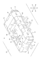
- FIG. 1 is an external perspective view showing a top view of the connector 1 according to an embodiment in which the first connector 10 and the second connector 50 are connected to each other.
- FIG. 2 is an external perspective view showing the connector 1 according to the embodiment in which the first connector 10 and the second connector 50 are separated from each other in a top view.
- the connector 1 has a first connector 10 and a second connector 50 that can be connected to each other.
- the first connector 10 has a first insulator 20, a first contact portion 34a described later, and a first contact 30a attached to the first insulator 20.
- the first connector 10 has a signal contact 30b and a first shielding member 40 attached to the first insulator 20.
- the second connector 50 has a second insulator 60 that can be fitted to the first insulator 20.
- the second connector 50 has a second contact portion 74a, which will be described later, in contact with the first contact portion 34a in a fitted state in which the first insulator 20 and the second insulator 60 are fitted, and is attached to the second insulator 60.
- the second connector 50 has a signal contact 70b and a second shielding member 80 attached to the second insulator 60.
- the shielding member of the connector 1 is attached to the first insulator 20 and the second insulator 60. More specifically, the shielding member includes a first shielding member 40 attached to the first insulator 20 and a second shielding member 80 attached to the second insulator 60.
- the second connector 50 will be described as a receptacle connector.
- the first connector 10 will be described as a plug connector.
- a second connector 50 in which the second contact 70a and the signal contact 70b are elastically deformed in a fitted state in which the first insulator 20 and the second insulator 60 are fitted to each other will be described as a receptacle connector.
- the first connector 10 in which the first contact 30a and the signal contact 30b are not elastically deformed will be described as a plug connector.
- the types of the first connector 10 and the second connector 50 are not limited thereto.
- the second connector 50 may serve as a plug connector
- the first connector 10 may serve as a receptacle connector.
- the first connector 10 and the second connector 50 will be described as being mounted on the circuit boards CB1 and CB2, respectively.
- the first connector 10 and the second connector 50 electrically connect the circuit board CB1 and the circuit board CB2 in a state of being connected to each other.
- the circuit boards CB1 and CB2 may be rigid boards, or may be any other circuit boards.
- at least one of the circuit boards CB1 and CB2 may be a flexible printed circuit board.
- first connector 10 and the second connector 50 will be described as being connected to each other in the direction perpendicular to the circuit boards CB1 and CB2.
- the first connector 10 and the second connector 50 are connected to each other in the vertical direction as an example.
- the connection method is not limited to this.
- the first connector 10 and the second connector 50 may be connected to each other in a direction parallel to the circuit boards CB1 and CB2.
- the first connector 10 and the second connector 50 are connected to each other so that one is perpendicular to the mounted circuit board and the other is parallel to the mounted circuit board. May be done.
- the “fitting direction” described in the claims corresponds to the vertical direction as an example in the present specification.
- the “first direction orthogonal to the fitting direction” corresponds to the left-right direction as an example.
- the “longitudinal direction of the connector 1" corresponds to the left-right direction as an example.
- the “first direction and the second direction orthogonal to the fitting direction” correspond to the front-rear direction as an example.
- the “short direction of the connector 1" corresponds to the front-back direction as an example.
- the “circuit board side in the mating direction” corresponds to the lower side as an example.
- the connector 1 has two pairs of first contacts 30a and second contacts 70a that are in contact with each other in a state where the first connector 10 and the second connector 50 are connected.
- the connector 1 has a shielding structure that shields a pair of first contacts 30a and second contacts 70a that are in contact with each other in a fitted state in which the first insulator 20 and the second insulator 60 are fitted.
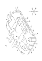
- FIG. 3 is an external perspective view showing the first connector 10 unit of FIG. 1 in a top view.
- FIG. 4 is an external perspective view showing the first connector 10 unit of FIG. 1 in a bottom view.
- the first connector 10 is obtained by integrally molding the first contact 30a, the signal contact 30b, the first shielding member 40, and the first insulator 20 by insert molding.
- the first insulator 20 constituting the first connector 10 is made of an insulating and heat-resistant synthetic resin material.
- the first insulator 20 extends in a plate shape in the left-right direction.
- the first insulator 20 has a bottom plate portion 21 that constitutes a lower portion, and an annular outer peripheral wall 22 that projects upward from the entire peripheral edge portion of the upper surface of the bottom plate portion 21.
- the outer peripheral wall 22 includes a pair of short walls 22a extending in the front-rear direction and a pair of longitudinal walls 22b extending in the left-right direction.
- the first insulator 20 has a fitting recess 23 formed by a space formed by a bottom plate portion 21 and an outer peripheral wall 22.
- the first insulator 20 has a first contact holding groove 24a formed from the lateral outer surface of the short wall 22a of the outer peripheral wall 22 to the inside of the short wall 22a.
- the first contact holding groove 24a integrally holds the first contact 30a.
- the first insulator 20 has a signal contact holding groove 24b formed over the outer surface and the inner surface in the front-rear direction on the longitudinal wall 22b of the outer peripheral wall 22.
- the signal contact holding groove 24b integrally holds the signal contact 30b.
- the first insulator 20 has a first shielding member holding groove 25 formed over the outer and inner surfaces in the left-right direction and the outer surface in the front-rear direction on the short wall 22a of the outer peripheral wall 22.
- the first shielding member holding groove 25 integrally holds the first shielding member 40.
- FIG. 5 is a perspective view showing the first connector 10 of FIG. 3 in a top view with only the first insulator 20 hidden.
- FIG. 6 is a perspective view showing only the pair of first shielding members 40 of FIG. 5 in a top view.
- FIG. 7 is a perspective view showing only the pair of first contacts 30a of FIG. 5 in a top view.
- Each configuration of the first contact 30a, the signal contact 30b, and the first shielding member 40 will be described in detail with reference mainly to FIGS. 5 to 7.
- the first contact 30a is formed by molding, for example, a thin plate of a copper alloy containing phosphor bronze, beryllium copper, or titanium copper or a Corson-based copper alloy into the shapes shown in FIGS. 5 and 7 using a progressive mold (stamping). It is a thing.
- the surface of the first contact 30a is plated with gold, tin, or the like after a base is formed by nickel plating.
- the first contact 30a has a mounting portion 31a extending outward in an L shape.
- the first contact 30a has a connecting portion 32a formed in a reverse taper shape upward from the upper end portion of the mounting portion 31a.
- the first contact 30a has a curved portion 33a extending upward from the connecting portion 32a in a U shape.
- the first contact 30a has a first contact portion 34a configured to include an outer surface in the left-right direction on the free end side of the curved portion 33a.
- the first contact 30a is held by the first contact holding groove 24a by integrating the first contact holding groove 24a with the entire portion other than the mounting portion 31a. There is.
- the first contact 30a is arranged along the lateral direction of the connector 1. When the first contact 30a is held in the first contact holding groove 24a of the first insulator 20, the tip of the mounting portion 31a of the first contact 30a is located outside the short wall 22a.
- the signal contact 30b is, for example, formed by molding a thin plate of a copper alloy containing phosphor bronze, beryllium copper, or titanium copper or a Corson-based copper alloy into the shape shown in FIG. 5 using a progressive mold (stamping).
- the surface of the signal contact 30b is plated with gold, tin, or the like after a base is formed by nickel plating.
- the signal contact 30b has a mounting portion 31b extending outward in an L shape.
- the signal contact 30b has a contact portion 32b extending upward from the upper end portion of the mounting portion 31b.
- the contact portion 32b has a contact surface formed of an inner surface in the front-rear direction.
- the contact portion 32b is formed wider in the left-right direction than the mounting portion 31b.
- the signal contact 30b has a curved portion 33b extending outward from the contact portion 32b in a U shape.
- the signal contact 30b has a contact portion 34b configured to include an outer surface in the front-rear direction on the free end side of the curved portion 33b.
- the signal contact 30b has a protrusion 35b formed on the upper part of the contact surface of the contact portion 32b.
- the free end of the curved portion 33b is formed at a height similar to that of the contact portion 32b.
- the signal contact 30b is integrally held with respect to the signal contact holding groove 24b by contacting the entire inner surface of the portion other than the mounting portion 31b with the signal contact holding groove 24b. Has been done.
- the tip of the mounting portion 31b of the signal contact 30b is located outside the longitudinal wall 22b.
- the first shielding member 40 is formed by molding a thin plate of an arbitrary metal material into the shapes shown in FIGS. 5 and 6 using a progressive remittance mold (stamping).
- the processing method of the first shielding member 40 includes a step of bending in the plate thickness direction after performing a punching process.
- the first shielding member 40 is integrally held with respect to the first shielding member holding groove 25 of the first insulator 20, and is arranged on both the left and right sides of the first insulator 20.
- the first shielding member 40 has a first base portion 41 that constitutes a lower end portion thereof.
- the first shielding member 40 has first extending portions 42 extending in an L shape from the first base portion 41 along the vertical direction and arranged on both sides of the first base portion 41 in the front-rear direction.
- the first shielding member 40 has a second extending portion 43 extending in a U shape along the vertical direction from a pair of edges of the first base portion 41 along the left-right direction.
- the first shielding member 40 has a connecting portion 44 that connects the first base portions 41 on both the front and rear sides at the inner end portion in the left-right direction thereof.
- the first shielding member 40 has a first shielding portion 45 extending in an L shape from the connecting portion 44 along the vertical direction and extending over the entire width of the connecting portion 44 in the front-rear direction.
- the first shielding member 40 has a mounting portion 46 formed by lower surfaces of the first base portions 41 on both front and rear sides.
- the mounting portions 46 arranged on both the front and rear sides of the first shielding member 40 are mounted in a separated state with respect to a pair of grounding patterns separated from each other on the mounting surface of the circuit board CB1, for example.
- the mounting portion 31a of the first contact 30a is soldered to the circuit pattern formed on the mounting surface of the circuit board CB1.
- the mounting portion 31b of the signal contact 30b is soldered to the circuit pattern formed on the mounting surface.
- the mounting portion 46 of the first shielding member 40 is soldered to the grounding pattern formed on the mounting surface.
- the first connector 10 is mounted on the circuit board CB1.
- the configuration of the second connector 50 will be described with reference mainly to FIGS. 8 to 13.
- FIG. 8 is an external perspective view showing the second connector 50 alone of FIG. 1 in a top view.
- FIG. 9 is an external perspective view showing the second connector 50 alone of FIG. 1 in a bottom view.
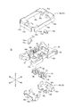
- FIG. 10 is an exploded perspective view of the second connector 50 of FIG. 8 when viewed from above.
- the second connector 50 is assembled by, for example, the following method.
- the second contact 70a is press-fitted into the second insulator 60 from above.
- the signal contact 70b is press-fitted into the second insulator 60 from below.
- the second shielding member 80 is press-fitted into the second insulator 60 from above and below.
- the second insulator 60 is a plate-shaped member extending in the left-right direction, which is formed by injection molding an insulating and heat-resistant synthetic resin material.
- the second insulator 60 has a bottom plate portion 61 that constitutes a lower portion, and an annular outer peripheral wall 62 that projects upward while surrounding the entire peripheral edge portion of the bottom plate portion 61 from the outside.
- the outer peripheral wall 62 includes a pair of short walls 62a extending in the front-rear direction and a pair of longitudinal walls 62b extending in the left-right direction.
- the second insulator 60 has a fitting convex portion 63 that projects upward from the central portion of the bottom plate portion 61.
- the second insulator 60 has a second contact holding groove 64a formed in the central portion of the outer peripheral wall 62 in the front-rear direction of the short wall 62a.
- the second contact holding groove 64a holds the press-fitted second contact 70a.
- the second insulator 60 has a signal contact holding groove 64b formed over the inner surface of the longitudinal wall 62b of the outer peripheral wall 62 in the front-rear direction and the outer surface of the fitting convex portion 63 in the front-rear direction.
- the signal contact holding groove 64b holds the press-fitted signal contact 70b.
- the second insulator 60 has a second shielding member holding groove 65 formed over the outer surface in the left-right direction, the outer surface in the front-rear direction, and the inside of the short wall 62a in the short wall 62a of the outer peripheral wall 62.
- the second shielding member holding groove 65 holds the press-fitted second shielding member 80.
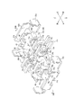
- FIG. 11 is a perspective view showing the second connector 50 of FIG. 8 in a top view with only the second insulator 60 hidden.
- FIG. 12 is a perspective view showing only the second shielding member 80 of FIG. 11 in a top view.
- FIG. 13 is a perspective view showing only the pair of second contacts 70a of FIG. 11 in a top view. Each configuration of the second contact 70a, the signal contact 70b, and the second shielding member 80 will be described in detail with reference to FIGS. 11 to 13.
- the second contact 70a shows, for example, a thin plate of a copper alloy or Corson-based copper alloy having spring elasticity containing phosphor bronze, beryllium copper, or titanium copper using a progressive mold (stamping) in FIGS. 11 and 13. It is molded into a shape.
- the surface of the second contact 70a is plated with gold, tin, or the like after a base is formed by nickel plating.
- the second contact 70a has a mounting portion 71a extending outward in an L shape.
- the second contact 70a has a locking portion 72a formed continuously upward from the upper end portion of the mounting portion 71a.
- the locking portion 72a is formed wider in the front-rear direction than the mounting portion 71a and the curved portion 73a described later.
- the second contact 70a has a curved portion 73a extending upward from the locking portion 72a in a U shape.
- the second contact 70a has a second contact portion 74a configured to include an inner surface in the left-right direction on the free end side of the curved portion 73a.
- the second contact portion 74a has spring elasticity so that it can be elastically deformed along the left-right direction.
- the second contact 70a is held with respect to the second contact holding groove 64a by locking the locking portion 72a with the second contact holding groove 64a.
- the second contact 70a is arranged along the lateral direction of the connector 1.
- the tip of the mounting portion 71a of the second contact 70a is located inside the outermost end of the short wall 62a in the left-right direction. To do.
- the signal contact 70b has a shape shown in FIGS. 10 and 11 using, for example, a thin plate of a copper alloy or Corson-based copper alloy having spring elasticity containing phosphor bronze, beryllium copper, or titanium copper using a progressive mold (stamping). It is molded into.
- the surface of the signal contact 70b is plated with gold, tin, or the like after a base is formed by nickel plating.
- the signal contact 70b has a mounting portion 71b extending outward in an L shape.
- the signal contact 70b has a pair of locking portions 72b including a portion continuously formed upward from the upper end portion of the mounting portion 71b and a portion that is separated from and opposed to the portion in the front-rear direction.
- the locking portion 72b is formed wider in the left-right direction than the mounting portion 71b and the curved portion 73b described later.
- the signal contact 70b has a curved portion 73b that connects a pair of locking portions 72b, an S-shaped elastic contact portion 74b that is continuous with the locking portion 72b formed inside, and an outer side to the tip portion of the elastic contact portion 74b. It has a contact portion 75b formed toward the surface.
- the signal contact 70b has a contact portion 76b including a protrusion protruding from the inner surface of the curved portion 73b in the front-rear direction.
- the free end of the elastic contact portion 74b is formed at a height similar to that of the contact portion 75b.
- the signal contact 70b is held with respect to the signal contact holding groove 64b by locking the locking portion 72b to the signal contact holding groove 64b.
- the elastic contact portion 74b can be elastically deformed in the front-rear direction in the signal contact holding groove 64b formed in the fitting convex portion 63. is there.
- the tip of the mounting portion 71b of the signal contact 70b is located inside the outermost end of the longitudinal wall 62b in the front-rear direction.
- the second shielding member 80 is formed by molding a thin plate of an arbitrary metal material into the shape shown in FIGS. 10 to 12 using a progressive remittance mold (stamping).
- the processing method of the second shielding member 80 includes a step of bending in the plate thickness direction after performing a punching process.
- the second shielding member 80 is held by the second insulator 60 by being press-fitted into the second shielding member holding groove 65 of the second insulator 60.
- the second shielding member 80 includes, for example, three members. More specifically, the second shielding member 80 includes a first member 80a attached from above to the second insulator 60 so as to surround the outer peripheral wall 62 from all sides. The second shielding member 80 includes a pair of second members 80b attached from below to the second insulator 60 so as to be arranged on the left and right sides of the second insulator 60.
- the second member 80b has a second base portion 81b constituting the lower end portion thereof.
- the second base 81b is adjacent to the second contact 70a in the left-right direction.
- the second member 80b has a second shielding portion 82b that extends in an L shape from the second base portion 81b along the vertical direction and extends over the entire width of the second base portion 81b in the front-rear direction.
- the second member 80b constitutes a central portion of the second base portion 81b, and has a third shielding portion 83b extending over the entire width of the second base portion 81b in the front-rear direction.
- the second member 80b has a locking portion 84b extending in an L shape along the vertical direction from a pair of edges of the second base portion 81b along the left-right direction.
- the second member 80b is arranged inside the locking portion 84b in the left-right direction, and has a contact portion 85b extending in an S-shape in the vertical direction from a pair of edges of the second base portion 81b along the left-right direction. Have.
- the contact portion 85b is formed at the inner end portion in the left-right direction of the second member 80b.
- the second member 80b has a first mounting portion 86b that is arranged inside the second contact 70a in the left-right direction and is mounted on the circuit board CB2.
- the first mounting portion 86b is formed in the second base portion 81b in an L shape on the opposite side in the left-right direction from the second contact 70a.
- the first mounting portion 86b is formed at the inner end portion in the left-right direction of the second member 80b.
- the pair of first mounting portions 86b are arranged on both front and rear sides of the second base portion 81b in one second member 80b.
- the first mounting portion 86b is arranged symmetrically on both sides with respect to the second contact 70a in the front-rear direction.
- the pair of first mounting portions 86b are mounted in a separated state with respect to a pair of circuit patterns that are separated from each other on the mounting surface of the circuit board CB2, for example.
- the second member 80b includes a second mounting portion 87b composed of lower surfaces on both front and rear sides and lower surfaces on both front and rear locking portions 84b at the outer end portions in the left-right direction of the second base portion 81b.
- the second mounting portion 87b arranged on the front side and the second mounting portion 87b arranged on the rear side are, for example, a pair separated from each other on the mounting surface of the circuit board CB2. It is mounted separately for the circuit pattern.
- the contact portion 85b extends upward from the first mounting portion 86b.
- the contact portion 85b extends from the outer end portion of the first mounting portion 86b in the front-rear direction. More specifically, the contact portion 85b extends in an S shape from the first mounting portion 86b and has spring elasticity.
- the contact portion 85b extends along the left-right direction between the first mounting portion 86b and the second contact 70a.
- the width of the contact portion 85b in the left-right direction is equal to or larger than the mounting width in the left-right direction of the first mounting portion 86b.
- the contact portions 85b are arranged symmetrically on both sides with respect to the second contact 70a in the front-rear direction.
- the second member 80b is held against the second shielding member holding groove 65 by locking the locking portion 84b and the second shielding portion 82b to the second shielding member holding groove 65.
- the pair of locking portions 84b are locked in the grooves formed inside both the front and rear sides of the short wall 62a of the second shielding member holding groove 65.
- the second shielding portion 82b is locked to the groove formed on the outer surface of the short wall 62a in the left-right direction of the second shielding member holding groove 65.
- the first member 80a has a third base portion 81a constituting the upper end portion thereof.
- the first member 80a has a fourth shielding portion 82a extending in the left-right direction with a predetermined width on the outer peripheral portion in the front-rear direction.
- the first member 80a has a fifth shielding portion 83a arranged further outside the second shielding portion 82b in the left-right direction.
- the fifth shielding portion 83a is wider in the front-rear direction than the second shielding portion 82b, and is arranged so as to overlap the entire second shielding portion 82b in the front-rear direction. As shown in FIG.
- the first member 80a has an outer peripheral side shielding portion 84a arranged outside the longitudinal wall 62b of the second insulator 60 along the left-right direction.
- the outer peripheral side shielding portion 84a extends along the left-right direction so as to connect the fourth shielding portions 82a located on both the left and right sides.
- the first member 80a has contact portions 85a extending from the third base portion 81a along the vertical direction and arranged on both sides with respect to the second contact 70a in the front-rear direction.
- the contact portion 85a has spring elasticity so that it can be elastically deformed along the left-right direction.
- the first member 80a has locking portions 86a formed at both ends in the left-right direction on the outer peripheral portion in the front-rear direction.
- the first member 80a has a first mounting portion 87a extending linearly downward from the lower end portions on both front and rear sides of the fifth shielding portion 83a.
- the first member 80a has a second mounting portion 88a that extends linearly downward from the lower end portion of the locking portion 86a.
- the first member 80a has a third mounting portion 89a that extends linearly downward from both left and right ends of the outer peripheral side shielding portion 84a.
- the first mounting portion 87a on the front side in the left direction and the second mounting portion 88a on the left side in the front direction, which are adjacent to each other, are mounted on the same grounding pattern on the mounting surface of the circuit board CB2.
- first mounting portion 87a on the rear side in the left direction and the second mounting portion 88a on the left side in the rear direction, which are adjacent to each other, are mounted on the same grounding pattern on the mounting surface of the circuit board CB2.
- the same is true on the right side of the first member 80a.
- the four third mounting portions 89a are mounted in a separated state with respect to the four grounding patterns that are separated from each other on the mounting surface of the circuit board CB2.
- the first member 80a is held with respect to the second shielding member holding groove 65 by engaging the locking portion 86a with the second shielding member holding groove 65.
- the mounting portion 71a of the second contact 70a is soldered to the circuit pattern formed on the mounting surface of the circuit board CB2.
- the mounting portion 71b of the signal contact 70b is soldered to the circuit pattern formed on the mounting surface.
- the first mounting portion 87a, the second mounting portion 88a, the third mounting portion 89a, and the second member 80b of the first member 80a of the second shielding member 80 The first mounting portion 86b and the second mounting portion 87b are soldered.
- the first mounting portion 87a on the left front side of the first member 80a, the second mounting portion 88a on the left side in the front direction, and the second mounting portion 87b on the front side of the second member 80b arranged on the left side are grounded in the same manner. Soldered to the pattern. The same applies to the rear side of the second member 80b arranged on the left side and the second member 80b arranged on the right side. Thereby, the two first member 80a and the second member 80b can be electrically regarded as one shielding member.
- the second connector 50 is mounted on the circuit board CB2.
- An electronic component other than the second connector 50 such as a CPU (Central Processing Unit), a controller, or a memory, is mounted on the mounting surface of the circuit board CB2.
- FIG. 14 is a perspective view showing the connector 1 of FIG. 1 in a top view with only the first insulator 20 and the second insulator 60 hidden.
- FIG. 15 is a cross-sectional view taken along the XV-XV arrow line of FIG.
- the configuration of the connector 1 in a fitted state in which the first connector 10 and the second connector 50 are connected and the first insulator 20 and the second insulator 60 are fitted is mainly described. explain.
- the first connector 10 and the second connector 50 face each other in the vertical direction while substantially matching the front-rear position and the left-right position. Let me.
- the first connector 10 is moved downward.
- the first connector 10 and the second connector 50 are connected to each other, and the mated state of the connector 1 is obtained.
- the fitting recess 23 of the first insulator 20 and the fitting protrusion 63 of the second insulator 60 are fitted to each other.
- the first contact portion 34a of the first contact 30a and the second contact portion 74a of the second contact 70a are in contact with each other, and the second contact portion 74a having spring elasticity is elastic outward in the left-right direction. Deform.
- the first contact 30a and the second contact 70a are brought into contact with each other at only one place by the first contact portion 34a and the second contact portion 74a.
- the protrusion 35b of the signal contact 30b moves downward and gets over the contact portion 75b of the signal contact 70b, and the contact portion 32b of the signal contact 30b and the contact portion 75b of the signal contact 70b come into contact with each other. ..
- the elastic contact portion 74b having spring elasticity is elastically deformed inward in the front-rear direction.
- the contact portion 34b of the signal contact 30b and the contact portion 76b of the signal contact 70b are in contact with each other.
- the signal contact 30b and the signal contact 70b come into contact with each other at two points by the contact portion 32b and the contact portion 75b, and by the contact portion 34b and the contact portion 76b.
- the first extending portion 42 of the first shielding member 40 and the contact portion 85a of the first member 80a of the second shielding member 80 are in contact with each other.
- the first extending portion 42 of the first shielding member 40 extends from the first base portion 41 along the vertical direction, and is arranged on both sides of the contact portion between the first contact 30a and the second contact 70a in the front-rear direction. ing. More specifically, the first extending portion 42 of the first shielding member 40 is arranged so as to be adjacent to the first contact portion 34a and the second contact portion 74a that are in contact with each other on both sides in the front-rear direction. Has been done.
- the contact portion 85a of the first member 80a extends along the vertical direction from the third base portion 81a arranged on the same side as the first base portion 41 in the vertical direction, and with the first contact 30a in the front-rear direction. It is arranged on both sides with respect to the contact portion with the second contact 70a. More specifically, the contact portion 85a of the first member 80a is arranged so as to be adjacent to the first contact portion 34a and the second contact portion 74a that are in contact with each other on both sides in the front-rear direction.
- the first shielding member 40 and the first member 80a are adjacent to the first contact portion 34a and the second contact portion 74a that are in contact with each other, and they are placed in the front-rear direction.
- the two pairs of the first extending portion 42 and the contact portion 85a sandwiching the contact portion make contact at two points.
- the two pairs of the first extending portion 42 and the contact portion 85a are arranged symmetrically on both sides with respect to the contact portion between the first contact 30a and the second contact 70a in the front-rear direction.
- the second extending portion 43 of the first shielding member 40 and the contact portion 85b of the second member 80b of the second shielding member 80 are in contact with each other.
- the second extending portion 43 of the first shielding member 40 extends from the first base portion 41 along the vertical direction, and is arranged on both sides of the contact portion between the first contact 30a and the second contact 70a in the front-rear direction. ing. More specifically, the second extending portion 43 of the first shielding member 40 is arranged so as to be close to the first contact portion 34a and the second contact portion 74a that are in contact with each other on both sides in the front-rear direction. Has been done.
- the contact portion 85b of the second member 80b extends in the vertical direction from the second base portion 81b arranged on the opposite side of the first base portion 41 in the vertical direction, and extends with the first contact 30a in the front-rear direction. It is arranged on both sides with respect to the contact portion with the second contact 70a. More specifically, the contact portion 85b of the second member 80b is arranged so as to be close to the first contact portion 34a and the second contact portion 74a that are in contact with each other on both sides in the front-rear direction.
- the first shielding member 40 and the second member 80b are brought close to each other in the front-rear direction while being close to the first contact portion 34a and the second contact portion 74a that are in contact with each other.
- the two pairs of the second extending portion 43 and the contact portion 85b sandwiching the contact portion make contact at two points.
- the two pairs of the second extending portion 43 and the contact portion 85b are arranged symmetrically on both sides with respect to the contact portion between the first contact 30a and the second contact 70a in the front-rear direction.
- the first shielding member 40 and the second shielding member 80 are located at four locations adjacent to or close to the first contact portion 34a and the second contact portion 74a that are in contact with each other. Contact.
- the first shielding portion 45 of the first shielding member 40 is arranged inside the first contact portion 34a and the second contact portion 74a that are in contact with each other in the left-right direction. ..
- the second shielding portion 82b of the second member 80b of the second shielding member 80 is arranged outside the first contact portion 34a and the second contact portion 74a that are in contact with each other in the left-right direction.
- the first contact portion 34a and the second contact portion 74a that are in contact with each other are shielded by the first shield portion 45 and the second shield portion 82b from both sides in the left-right direction.
- the third shielding portion 83b of the second member 80b of the second shielding member 80 is fitted in the vertical direction with respect to the first contact portion 34a and the second contact portion 74a that are in contact with each other. It is located on the opposite side of the side. In this way, the first contact portion 34a and the second contact portion 74a that are in contact with each other are shielded by the third shielding portion 83b from the side opposite to the fitting side.
- the fourth shielding portion 82a of the first member 80a of the second shielding member 80 is on both sides with respect to the first contact portion 34a and the second contact portion 74a that are in contact with each other in the front-rear direction. Have been placed. In this way, the first contact portion 34a and the second contact portion 74a that are in contact with each other are shielded by the fourth shielding portion 82a from both sides in the front-rear direction.
- the fifth shielding portion 83a of the first member 80a of the second shielding member 80 is arranged further outside the second shielding portion 82b in the left-right direction. In this way, the first contact portion 34a and the second contact portion 74a that are in contact with each other are shielded by the double structure of the second shielding portion 82b and the fifth shielding portion 83a on the outside in the left-right direction.
- the connector 1 According to the connector 1 according to the above embodiment, a good noise shielding effect can be obtained.
- the first shielding portion 45 and the second shielding portion 82b shield the first contact portion 34a and the second contact portion 74a that are in contact with each other from both sides in the left-right direction, and the third shielding portion 83b is on the fitting side. Shield from the other side.
- the first contact portion 34a and the second contact portion 74a that are in contact with each other are shielded from at least three directions. Therefore, the inflow of noise from the outside to the first contact 30a and the second contact 70a and the outflow of noise from the first contact 30a and the second contact 70a to the outside are effectively suppressed.
- the third shielding portion 83b shields the first contact portion 34a and the second contact portion 74a that are in contact with each other from the side opposite to the fitting side, so that the first contact 30a and the second contact 70a and the circuit board CB2
- the noise shielding effect between the two is improved. More specifically, the inflow of noise from the circuit board CB2 to the first contact 30a and the second contact 70a and the outflow of noise from the first contact 30a and the second contact 70a to the circuit board CB2 are effectively suppressed. To. As a result, for example, even in high-speed transmission, it is possible to maintain good transmission characteristics for high-frequency signals without depending on the circuit configuration of the circuit board CB2.
- the shielding member includes a first shielding member 40 attached to the first insulator 20 and a second shielding member 80 attached to the second insulator 60.
- the first shielding portion 45 is formed on the first shielding member 40
- the second shielding portion 82b and the third shielding portion 83b are formed on the second shielding member 80.
- the first shielding member 40 and the second shielding member 40 2 The shape of the shielding member 80 is simplified.
- the third shielding portion 83b which corresponds to the lower surface of the shielding portion
- the second shielding portion 82b which corresponds to the left surface of the shielding portion
- the gap between the lower surface and the left surface is eliminated, and at the same time, the first 3
- the shielding portion 83b and the second shielding portion 82b can be surely conductive. Therefore, a higher noise shielding effect can be obtained.
- the second shielding member 80 has a fourth shielding portion 82a arranged on both sides of the first contact portion 34a and the second contact portion 74a that are in contact with each other in the front-rear direction.
- the shielding member has five shielding portions together with the first shielding portion 45, the second shielding portion 82b, and the third shielding portion 83b.
- the second shielding member 80 has a fifth shielding portion 83a arranged further outside the second shielding portion 82b in the left-right direction.
- the second shielding member 80 doubles the second shielding portion 82b and the fifth shielding portion 83a on the outside in the left-right direction with respect to the first contact portion 34a and the second contact portion 74a that are in contact with each other.
- the noise shielding effect from the left-right direction is particularly improved, and the inflow of noise from the outside to the first contact 30a and the second contact 70a and the outflow of noise from the first contact 30a and the second contact 70a to the outside are caused. It is suppressed more effectively.
- the second shielding member 80 has an outer peripheral side shielding portion 84a arranged outside the second insulator 60 along the left-right direction.
- the second shielding member 80 has a shielding portion on the outside in the front-rear direction with respect to the signal contact 30b and the signal contact 70b that are in contact with each other.
- the noise shielding effect is improved for the signal contact 30b and the signal contact 70b. More specifically, the inflow of noise from the outside to the signal contact 30b and the signal contact 70b and the outflow of noise from the signal contact 30b and the signal contact 70b to the outside are effectively suppressed. As a result, it is possible to obtain good transmission characteristics for high-frequency signals even in high-speed transmission, for example.
- the pair of first contacts 30a are arranged at both ends of the first insulator 20 in the left-right direction along the lateral direction of the connector 1.
- the pair of second contacts 70a are arranged at both ends of the second insulator 60 in the left-right direction along the lateral direction of the connector 1.
- the connector 1 Since the connector 1 has a plurality of signal contacts 30b and signal contacts 70b different from the first contact 30a and the second contact 70a, the connector 1 has various kinds of signals between the circuit board CB1 and the circuit board CB2. Can be transmitted. Since the plurality of signal contacts 30b and signal contacts 70b are arranged along the longitudinal direction of the connector 1, they are far from the first contact 30a and the second contact 70a arranged along the lateral direction of the connector 1. Separate. The signal contact 30b and the signal contact 70b can be separated from the first contact 30a and the second contact 70a in the connector 1. Therefore, the signal contact 30b and the signal contact 70b can be shielded by using independent shielding members. At this time, since a sufficient space can be secured for providing the shielding member, it is possible to shield from multiple directions.
- the shape, arrangement, orientation, and number of each component described above are not limited to the contents shown in the above description and drawings.
- the shape, arrangement, orientation, and number of each component may be arbitrarily configured as long as the function can be realized.
- the method of assembling the first connector 10 and the second connector 50 described above is not limited to the contents of the above description.
- the method for assembling the first connector 10 and the second connector 50 may be any method as long as they can be assembled so as to exhibit their respective functions.
- at least one of the first contact 30a, the signal contact 30b, and the first shielding member 40 may be attached to the first insulator 20 by press fitting instead of insert molding.
- at least one of the second contact 70a, the signal contact 70b, and the second shielding member 80 may be integrally molded with the second insulator 60 by insert molding instead of press fitting.
- the shielding member has the first shielding member 40 and the second shielding member 80, but the configuration of the shielding member is not limited to this.
- the shielding member may be integrally formed and attached to at least one of the first insulator 20 and the second insulator 60 in the fitted state.
- each shielding portion including the fourth shielding portion 82a, the fifth shielding portion 83a, and the outer peripheral side shielding portion 84a is the first shielding portion. It may be formed on either the shielding member 40 or the second shielding member 80. For example, all the shielding portions may be formed only on the second shielding member 80. Each shielding portion may be formed in a state of being divided into both the first shielding member 40 and the second shielding member 80.
- the third shielding portion 83b is arranged directly below the first contact portion 34a and the second contact portion 74a that are in contact with each other.
- the third shielding portion 83b may be arranged at a position shifted in the left-right direction with respect to the first contact portion 34a and the second contact portion 74a that are in contact with each other.
- the second shielding member 80 has a fourth shielding portion 82a arranged on both sides with respect to the first contact portion 34a and the second contact portion 74a in contact with each other, but the present invention is limited to this. Not done.
- the second shielding member 80 may or may not have the fourth shielding portion 82a on only one side as long as a good noise shielding effect can be obtained.
- FIG. 16 is a perspective view corresponding to FIG. 14, showing a modified example of the connector 1 of FIG. 1 in a top view with only the first insulator 20 and the second insulator 60 hidden.
- FIG. 17 is a cross-sectional view taken along the line XVII-XVII of FIG.
- the second shielding member 80 does not have the first member 80a, but has only the second member 80b.
- the second shielding member 80 has the fifth shielding portion 83a, but the present invention is not limited to this.
- the second shielding member 80 does not have to have the fifth shielding portion 83a as long as a good noise shielding effect can be obtained.
- the second shielding member 80 has the outer peripheral side shielding portion 84a, but the present invention is not limited to this.
- the second shielding member 80 does not have to have the outer peripheral side shielding portion 84a as long as a good noise shielding effect can be obtained.
- the shielding member has a first shielding portion 45, a second shielding portion 82b, a third shielding portion 83b, a fourth shielding portion 82a, and a fifth shielding portion 83a, but the present invention is not limited thereto. ..
- the shielding member in addition to the first shielding portion 45 to the fifth shielding portion 83a, is on the side opposite to the third shielding portion 83b in the vertical direction with respect to the first contact portion 34a and the second contact portion 74a that are in contact with each other. It may have a sixth shielding portion arranged in.
- the sixth shielding portion may be formed on either one of the first shielding member 40 and the second shielding member 80.
- the sixth shielding portion shields the first contact portion 34a and the second contact portion 74a that are in contact with each other from above. Therefore, the first shielding portion 45 to the fifth shielding portion 83a and the sixth shielding portion shield the first contact portion 34a and the second contact portion 74a that are in contact with each other from the six directions of front, back, left, right, up and down, so that noise is generated. The shielding effect is further improved.
- the first extending portion 42 of the first shielding member 40 and the contact portion 85a of the second shielding member 80 are formed on both sides of the contact portion between the first contact 30a and the second contact 70a in the front-rear direction.
- they are in contact with each other, but are not limited to this.
- the second shielding member 80 does not have the contact portion 85a, and only the first extending portion 42 of the first shielding member 40 is the first. It may be arranged on both sides of the contact portion between the first contact 30a and the second contact 70a.
- first base portion 41 and the first extending portion 42 are formed on the first shielding member 40, but the present invention is not limited to this.
- Each component including the first base portion 41 and the first extending portion 42 may be formed on either one of the first shielding member 40 and the second shielding member 80.
- Each component may be formed in a state of being divided into both the first shielding member 40 and the second shielding member 80.
- the two pairs of the second extending portion 43 and the contact portion 85b are symmetrically arranged on both sides with respect to the contact portion between the first contact 30a and the second contact 70a in the front-rear direction.
- the two pairs of the second extending portion 43 and the contact portion 85b may be arranged asymmetrically as long as good transmission characteristics can be obtained.
- two pairs of the first extending portion 42 and the contact portion 85a are symmetrically arranged on both sides with respect to the contact portion between the first contact 30a and the second contact 70a in the front-rear direction.
- the two pairs of the first extending portion 42 and the contact portion 85a may be arranged asymmetrically as long as good transmission characteristics can be obtained.
- the contact portion 85b of the second shielding member 80 extends between the first mounting portion 86b and the second contact 70a along the left-right direction, but the present invention is not limited to this.
- the contact portion 85b of the second shielding member 80 may extend along an arbitrary direction.
- the width of the contact portion 85b of the second shielding member 80 in the left-right direction is equal to or larger than the mounting width of the first mounting portion 86b in the left-right direction, but the present invention is not limited to this.
- the width of the contact portion 85b in the left-right direction may be smaller than the width of the first mounting portion 86b in the left-right direction.
- the contact portion 85b of the second shielding member 80 extends in an S shape from the first mounting portion 86b, but the present invention is not limited to this.
- the contact portion 85b may extend from the first mounting portion 86b in any shape.
- the contact portion 85b of the second shielding member 80 has spring elasticity, but the present invention is not limited to this.
- the contact portion 85b does not have to have spring elasticity.
- the second extension 43 that comes into contact with the contact 85b may have spring elasticity.
- first contact 30a and the second contact 70a are arranged along the lateral direction of the connector 1, but the present invention is not limited to this.
- the first contact 30a and the second contact 70a may be arranged along the longitudinal direction of the connector 1. It has been explained that the pair of first contacts 30a are arranged at both ends of the first insulator 20 in the left-right direction, and the pair of second contacts 70a are arranged at both ends of the second insulator 60 in the left-right direction. Not limited.
- the pair of first contacts 30a may be arranged inside the first insulator 20 in the left-right direction, and the pair of second contacts 70a may be arranged inside the second insulator 60 in the left-right direction.
- the connector 1 has a plurality of contacts different from the first contact 30a and the second contact 70a, that is, the signal contact 30b and the signal contact 70b, but the present invention is not limited thereto.
- the connector 1 does not have to have the signal contact 30b and the signal contact 70b.
- these plurality of contacts are arranged along the longitudinal direction of the connector 1, but the present invention is not limited to this. These plurality of contacts may be arranged along the lateral direction of the connector 1.
- the second shielding member 80 has been described as having the first member 80a and the second member 80b, but the present invention is not limited thereto.
- the second shielding member 80 may be integrally formed as one member without being separated into two members.
- each mounting unit in the above embodiment is not limited to the above description.
- Each mounting unit may be mounted in an arbitrary mounting pattern on the mounting surface of the corresponding circuit board.
- the connector 1 as described above is mounted on an electronic device including the circuit board CB1 and the circuit board CB2.
- Electronic devices include, for example, any communication terminal device such as a smartphone, and any information processing device such as a personal computer, copier, printer, facsimile, and multifunction device.
- Other electronic devices include any industrial device.
- Such an electronic device can obtain a good noise shielding effect at the connector 1.
- Such electronic devices have good transmission characteristics in signal transmission. Therefore, the reliability of the electronic device as a product is improved.
Landscapes
- Details Of Connecting Devices For Male And Female Coupling (AREA)
- Coupling Device And Connection With Printed Circuit (AREA)
Abstract
Description
回路基板に実装されるコネクタであって、
第1インシュレータと、第1接触部を有し、前記第1インシュレータに取り付けられている一対の第1コンタクトと、を有する第1コネクタと、
前記第1インシュレータに対して嵌合可能な第2インシュレータと、前記第1インシュレータと前記第2インシュレータとが嵌合する嵌合状態で前記第1接触部と接触する第2接触部を有し、前記第2インシュレータに取り付けられている一対の第2コンタクトと、を有する第2コネクタと、
前記第1インシュレータ及び前記第2インシュレータに取り付けられている遮蔽部材と、
を備え、
前記遮蔽部材は、
前記嵌合状態で互いに接触している前記第1接触部及び前記第2接触部に対し、前記第1インシュレータと前記第2インシュレータとが嵌合する嵌合方向と直交する第1方向において、内側及び外側にそれぞれ配置されている第1遮蔽部及び第2遮蔽部と、
前記嵌合状態で互いに接触している前記第1接触部及び前記第2接触部に対し前記嵌合方向における前記回路基板側に配置されている第3遮蔽部と、
を有する。
上記のコネクタを備える。
10 第1コネクタ
20 第1インシュレータ
21 底板部
22 外周壁
22a 短手壁
22b 長手壁
23 嵌合凹部
24a 第1コンタクト保持溝
24b 信号コンタクト保持溝
25 第1遮蔽部材保持溝
30a 第1コンタクト
30b 信号コンタクト(コンタクト)
31a 実装部
31b 実装部
32a 接続部
32b 接触部
33a 湾曲部
33b 湾曲部
34a 第1接触部
34b 接触部
35b 突起
40 第1遮蔽部材
41 第1基部
42 第1延出部
43 第2延出部
44 連結部
45 第1遮蔽部
46 実装部
50 第2コネクタ
60 第2インシュレータ
61 底板部
62 外周壁
62a 短手壁
62b 長手壁
63 嵌合凸部
64a 第2コンタクト保持溝
64b 信号コンタクト保持溝
65 第2遮蔽部材保持溝
70a 第2コンタクト
70b 信号コンタクト(コンタクト)
71a 実装部
71b 実装部
72a 係止部
72b 係止部
73a 湾曲部
73b 湾曲部
74a 第2接触部
74b 弾性接触部
75b 接触部
76b 接触部
80 第2遮蔽部材
80a 第1部材
80b 第2部材
81a 第3基部
81b 第2基部
82a 第4遮蔽部
82b 第2遮蔽部
83a 第5遮蔽部
83b 第3遮蔽部
84a 外周側遮蔽部
84b 係止部
85a 接触部
85b 接触部
86a 係止部
86b 第1実装部
87a 第1実装部
87b 第2実装部
88a 第2実装部
89a 第3実装部
CB1 回路基板
CB2 回路基板
Claims (8)
- 回路基板に実装されるコネクタであって、
第1インシュレータと、第1接触部を有し、前記第1インシュレータに取り付けられている一対の第1コンタクトと、を有する第1コネクタと、
前記第1インシュレータに対して嵌合可能な第2インシュレータと、前記第1インシュレータと前記第2インシュレータとが嵌合する嵌合状態で前記第1接触部と接触する第2接触部を有し、前記第2インシュレータに取り付けられている一対の第2コンタクトと、を有する第2コネクタと、
前記第1インシュレータ及び前記第2インシュレータに取り付けられている遮蔽部材と、
を備え、
前記遮蔽部材は、
前記嵌合状態で互いに接触している前記第1接触部及び前記第2接触部に対し、前記第1インシュレータと前記第2インシュレータとが嵌合する嵌合方向と直交する第1方向において、内側及び外側にそれぞれ配置されている第1遮蔽部及び第2遮蔽部と、
前記嵌合状態で互いに接触している前記第1接触部及び前記第2接触部に対し前記嵌合方向における前記回路基板側に配置されている第3遮蔽部と、
を有する、
コネクタ。 - 前記遮蔽部材は、前記第1インシュレータに取り付けられている第1遮蔽部材と、前記第2インシュレータに取り付けられている第2遮蔽部材と、を有し、
前記第1遮蔽部は、前記第1遮蔽部材に形成され、
前記第2遮蔽部及び前記第3遮蔽部は、前記第2遮蔽部材に形成されている、
請求項1に記載のコネクタ。 - 前記第2遮蔽部材は、前記第1方向及び前記嵌合方向と直交する第2方向において、前記嵌合状態で互いに接触している前記第1接触部及び前記第2接触部に対し両側に配置されている第4遮蔽部を有する、
請求項2に記載のコネクタ。 - 前記第2遮蔽部材は、前記第1方向において、前記第2遮蔽部よりもさらに外側に配置されている第5遮蔽部を有する、
請求項2又は3に記載のコネクタ。 - 前記第2遮蔽部材は、前記第1方向に沿って前記第2インシュレータの外側に配置されている外周側遮蔽部を有する、
請求項2乃至4のいずれか1項に記載のコネクタ。 - 前記第1方向は、前記コネクタの長手方向であり、
一対の前記第1コンタクトは、前記第1インシュレータの前記長手方向の両端で、前記コネクタの短手方向に沿って配置され、
一対の前記第2コンタクトは、前記第2インシュレータの前記長手方向の両端で、前記コネクタの短手方向に沿って配置されている、
請求項1乃至5のいずれか1項に記載のコネクタ。 - 前記第1コンタクト及び前記第2コンタクトとは異なる複数のコンタクトを備え、
前記複数のコンタクトは、前記コネクタの長手方向に沿って配置されている、
請求項1乃至6のいずれか1項に記載のコネクタ。 - 請求項1乃至7のいずれか1項に記載のコネクタを備える電子機器。
Priority Applications (4)
| Application Number | Priority Date | Filing Date | Title |
|---|---|---|---|
| EP20907641.3A EP4084232B1 (en) | 2019-12-25 | 2020-12-21 | Connector and electronic apparatus |
| US17/782,542 US12142860B2 (en) | 2019-12-25 | 2020-12-21 | Connector and electronic apparatus |
| CN202080083370.XA CN114830449B (zh) | 2019-12-25 | 2020-12-21 | 连接器以及电子设备 |
| KR1020227013164A KR102611053B1 (ko) | 2019-12-25 | 2020-12-21 | 커넥터 및 전자기기 |
Applications Claiming Priority (2)
| Application Number | Priority Date | Filing Date | Title |
|---|---|---|---|
| JP2019235161A JP7244412B2 (ja) | 2019-12-25 | 2019-12-25 | コネクタ及び電子機器 |
| JP2019-235161 | 2019-12-25 |
Publications (1)
| Publication Number | Publication Date |
|---|---|
| WO2021132186A1 true WO2021132186A1 (ja) | 2021-07-01 |
Family
ID=76574107
Family Applications (1)
| Application Number | Title | Priority Date | Filing Date |
|---|---|---|---|
| PCT/JP2020/047758 Ceased WO2021132186A1 (ja) | 2019-12-25 | 2020-12-21 | コネクタ及び電子機器 |
Country Status (6)
| Country | Link |
|---|---|
| US (1) | US12142860B2 (ja) |
| EP (1) | EP4084232B1 (ja) |
| JP (1) | JP7244412B2 (ja) |
| KR (1) | KR102611053B1 (ja) |
| CN (1) | CN114830449B (ja) |
| WO (1) | WO2021132186A1 (ja) |
Families Citing this family (4)
| Publication number | Priority date | Publication date | Assignee | Title |
|---|---|---|---|---|
| JP7244412B2 (ja) * | 2019-12-25 | 2023-03-22 | 京セラ株式会社 | コネクタ及び電子機器 |
| JP7648472B2 (ja) * | 2021-08-10 | 2025-03-18 | 京セラ株式会社 | コネクタ及び電子機器 |
| JP7177417B1 (ja) * | 2022-08-10 | 2022-11-24 | Smk株式会社 | 基板対基板用コネクタ |
| CN115799920A (zh) * | 2022-12-30 | 2023-03-14 | 深圳市深台帏翔电子有限公司 | 连接器、电路板组件和电子设备 |
Citations (7)
| Publication number | Priority date | Publication date | Assignee | Title |
|---|---|---|---|---|
| JP2006059589A (ja) * | 2004-08-18 | 2006-03-02 | Hirose Electric Co Ltd | シールド付き電気コネクタ |
| JP2010157368A (ja) * | 2008-12-26 | 2010-07-15 | Jst Mfg Co Ltd | 電気コネクタ |
| JP2013041771A (ja) * | 2011-08-18 | 2013-02-28 | Smk Corp | 接続コネクタ |
| JP2013522857A (ja) * | 2010-03-22 | 2013-06-13 | スリーエム イノベイティブ プロパティズ カンパニー | 基板同士接続コネクター |
| JP2016012553A (ja) * | 2014-06-05 | 2016-01-21 | 株式会社村田製作所 | コネクタセット及びコネクタ |
| JP2018110087A (ja) * | 2017-01-06 | 2018-07-12 | ヒロセ電機株式会社 | 遮蔽シールド板付きコネクタ |
| JP2019087382A (ja) | 2017-11-06 | 2019-06-06 | 第一精工株式会社 | 電気コネクタ装置 |
Family Cites Families (57)
| Publication number | Priority date | Publication date | Assignee | Title |
|---|---|---|---|---|
| JP3079738B2 (ja) * | 1992-02-05 | 2000-08-21 | 富士通株式会社 | 基板用シールドマルチコネクタ |
| JP2004319257A (ja) * | 2003-04-16 | 2004-11-11 | Japan Aviation Electronics Industry Ltd | 平衡伝送用コネクタ |
| TWM250431U (en) * | 2003-08-08 | 2004-11-11 | Hon Hai Prec Ind Co Ltd | Electrical connector |
| TWM251313U (en) * | 2003-08-13 | 2004-11-21 | Hon Hai Prec Ind Co Ltd | Electrical connector |
| CN2667690Y (zh) * | 2003-09-06 | 2004-12-29 | 富士康(昆山)电脑接插件有限公司 | 电连接器 |
| TWM253928U (en) * | 2003-10-31 | 2004-12-21 | Hon Hai Prec Ind Co Ltd | Electrical connector |
| US7137825B2 (en) * | 2004-03-31 | 2006-11-21 | Tyco Electronics Corporation | Shielded electrical jack connector |
| TWI249886B (en) * | 2004-06-18 | 2006-02-21 | Hon Hai Prec Ind Co Ltd | Electrical connector |
| CN2736999Y (zh) * | 2004-09-23 | 2005-10-26 | 富士康(昆山)电脑接插件有限公司 | 电连接器组合 |
| CN2757356Y (zh) * | 2004-12-01 | 2006-02-08 | 富士康(昆山)电脑接插件有限公司 | 电连接器 |
| US7108567B1 (en) * | 2005-11-07 | 2006-09-19 | Hon Hai Precision Ind. Co., Ltd | Electrical device for interconnecting two printed circuit boards at a large distance |
| US7168986B1 (en) * | 2006-03-21 | 2007-01-30 | Cheng Uei Precision Industry Co., Ltd. | Board-to-board connector assembly with EMI shielding shields |
| JP4984823B2 (ja) * | 2006-10-26 | 2012-07-25 | 富士通株式会社 | シールド板およびシールド板が取り付けられる基板実装型コネクタ |
| JP4333884B2 (ja) * | 2007-03-01 | 2009-09-16 | 日本航空電子工業株式会社 | コネクタ |
| CN201204309Y (zh) * | 2008-03-25 | 2009-03-04 | 富士康(昆山)电脑接插件有限公司 | 电连接器 |
| JP4691738B2 (ja) * | 2008-09-01 | 2011-06-01 | ヒロセ電機株式会社 | シールド機能を有するコネクタ装置 |
| CN102217148A (zh) * | 2008-10-22 | 2011-10-12 | Fci公司 | 屏蔽连接器 |
| JP4901944B2 (ja) * | 2009-12-03 | 2012-03-21 | ヒロセ電機株式会社 | 電気コネクタ |
| CN201608308U (zh) * | 2009-12-26 | 2010-10-13 | 富士康(昆山)电脑接插件有限公司 | 电连接器 |
| US20110250800A1 (en) * | 2010-04-12 | 2011-10-13 | Hon Hai Precision Industry Co., Ltd. | Board to board connector assembly having improved plug and receptacle contacts |
| JP5890117B2 (ja) * | 2011-07-07 | 2016-03-22 | 日本航空電子工業株式会社 | コネクタ |
| JP5971845B2 (ja) * | 2012-06-04 | 2016-08-17 | 日本航空電子工業株式会社 | コネクタ |
| US8888506B2 (en) * | 2013-01-29 | 2014-11-18 | Japan Aviation Electronics Industry, Limited | Connector |
| KR101489117B1 (ko) * | 2013-02-27 | 2015-02-02 | 파나소닉 주식회사 | 커넥터 및 상기 커넥터에 이용되는 헤더 및 소켓 |
| JP6045953B2 (ja) * | 2013-03-28 | 2016-12-14 | 京セラコネクタプロダクツ株式会社 | コネクタ |
| KR101496720B1 (ko) * | 2013-11-08 | 2015-02-27 | (주)우주일렉트로닉스 | 실드 및 체결형 보드 커넥터 |
| US9391398B2 (en) * | 2014-03-20 | 2016-07-12 | Japan Aviation Electronics Industry, Limited | Connector assembly |
| US9525246B2 (en) * | 2014-05-05 | 2016-12-20 | Tyco Electronics Corporation | Printed circuit board connector assembly having contact shield with integral securing members |
| JP6167997B2 (ja) * | 2014-06-05 | 2017-07-26 | 株式会社村田製作所 | コネクタセット及びコネクタ |
| JP6391517B2 (ja) * | 2015-03-30 | 2018-09-19 | モレックス エルエルシー | コネクタ |
| JP6378642B2 (ja) * | 2015-04-23 | 2018-08-22 | モレックス エルエルシー | コネクタ |
| JP6513509B2 (ja) * | 2015-07-01 | 2019-05-15 | 日本航空電子工業株式会社 | 基板対基板コネクタおよびコネクタ |
| US10084265B2 (en) * | 2015-07-29 | 2018-09-25 | Dai-Ichi Seiko Co., Ltd. | Board-connecting electric connector device |
| JP6179564B2 (ja) * | 2015-07-29 | 2017-08-16 | 第一精工株式会社 | 基板接続用電気コネクタ |
| KR102030023B1 (ko) * | 2015-08-05 | 2019-10-08 | 교세라 가부시키가이샤 | 플러그 커넥터 |
| US9893480B2 (en) * | 2015-09-04 | 2018-02-13 | Tyco Electronics Japan G.K. | Connector |
| KR102420101B1 (ko) * | 2015-12-07 | 2022-07-13 | 삼성전자주식회사 | 케이블 지지구조를 포함하는 전자 기기 |
| JP6498622B2 (ja) * | 2016-03-14 | 2019-04-10 | 日本航空電子工業株式会社 | コネクタ |
| US10777941B2 (en) * | 2016-08-04 | 2020-09-15 | Kyocera Corporation | Connector |
| US10862234B2 (en) * | 2016-08-04 | 2020-12-08 | Kyocera Corporation | Electrical contact terminal |
| CN108232526B (zh) * | 2016-12-21 | 2020-04-24 | 富士康(昆山)电脑接插件有限公司 | 电连接器及其组合 |
| CN207925768U (zh) * | 2017-01-11 | 2018-09-28 | 富士康(昆山)电脑接插件有限公司 | 电连接器及其组合 |
| JP6950740B2 (ja) * | 2017-07-24 | 2021-10-13 | 株式会社村田製作所 | コネクタセット |
| JP6582083B2 (ja) * | 2018-03-09 | 2019-09-25 | 京セラ株式会社 | コネクタ及び電子機器 |
| JP6582082B2 (ja) * | 2018-03-09 | 2019-09-25 | 京セラ株式会社 | コネクタ及び電子機器 |
| JP6971182B2 (ja) * | 2018-03-23 | 2021-11-24 | 京セラ株式会社 | コネクタ及び電子機器 |
| KR101975811B1 (ko) * | 2018-04-10 | 2019-05-08 | (주)연호엠에스 | 전기 커넥터 |
| US10498058B1 (en) * | 2018-05-11 | 2019-12-03 | Molex, Llc | Connector and connector assembly |
| CN209571614U (zh) * | 2019-04-18 | 2019-11-01 | 富士康(昆山)电脑接插件有限公司 | 电连接器及其对接连接器 |
| CN216872292U (zh) * | 2019-06-24 | 2022-07-01 | 株式会社村田制作所 | 电连接器以及具备该电连接器的电连接器套件 |
| CN113924700B (zh) * | 2019-08-01 | 2024-04-12 | 株式会社村田制作所 | 阴型多极连接器以及具备该阴型多极连接器的多极连接器组 |
| JP7349635B2 (ja) * | 2019-09-30 | 2023-09-25 | パナソニックIpマネジメント株式会社 | コネクタ並びにそれに用いるソケット及びヘッダ |
| JP7418202B2 (ja) * | 2019-12-25 | 2024-01-19 | 京セラ株式会社 | コネクタ及び電子機器 |
| JP7244412B2 (ja) * | 2019-12-25 | 2023-03-22 | 京セラ株式会社 | コネクタ及び電子機器 |
| JP7201580B2 (ja) * | 2019-12-25 | 2023-01-10 | 京セラ株式会社 | コネクタ、コネクタモジュール、及び電子機器 |
| KR102494901B1 (ko) * | 2020-05-13 | 2023-02-06 | 니혼 고꾸 덴시 고교 가부시끼가이샤 | 커넥터 조립체 및 커넥터 |
| JP7484062B2 (ja) * | 2020-08-17 | 2024-05-16 | ヒロセ電機株式会社 | 基板接続コネクタ |
-
2019
- 2019-12-25 JP JP2019235161A patent/JP7244412B2/ja active Active
-
2020
- 2020-12-21 EP EP20907641.3A patent/EP4084232B1/en active Active
- 2020-12-21 US US17/782,542 patent/US12142860B2/en active Active
- 2020-12-21 CN CN202080083370.XA patent/CN114830449B/zh active Active
- 2020-12-21 WO PCT/JP2020/047758 patent/WO2021132186A1/ja not_active Ceased
- 2020-12-21 KR KR1020227013164A patent/KR102611053B1/ko active Active
Patent Citations (7)
| Publication number | Priority date | Publication date | Assignee | Title |
|---|---|---|---|---|
| JP2006059589A (ja) * | 2004-08-18 | 2006-03-02 | Hirose Electric Co Ltd | シールド付き電気コネクタ |
| JP2010157368A (ja) * | 2008-12-26 | 2010-07-15 | Jst Mfg Co Ltd | 電気コネクタ |
| JP2013522857A (ja) * | 2010-03-22 | 2013-06-13 | スリーエム イノベイティブ プロパティズ カンパニー | 基板同士接続コネクター |
| JP2013041771A (ja) * | 2011-08-18 | 2013-02-28 | Smk Corp | 接続コネクタ |
| JP2016012553A (ja) * | 2014-06-05 | 2016-01-21 | 株式会社村田製作所 | コネクタセット及びコネクタ |
| JP2018110087A (ja) * | 2017-01-06 | 2018-07-12 | ヒロセ電機株式会社 | 遮蔽シールド板付きコネクタ |
| JP2019087382A (ja) | 2017-11-06 | 2019-06-06 | 第一精工株式会社 | 電気コネクタ装置 |
Non-Patent Citations (1)
| Title |
|---|
| See also references of EP4084232A4 |
Also Published As
| Publication number | Publication date |
|---|---|
| US12142860B2 (en) | 2024-11-12 |
| US20230006376A1 (en) | 2023-01-05 |
| CN114830449A (zh) | 2022-07-29 |
| EP4084232A1 (en) | 2022-11-02 |
| EP4084232B1 (en) | 2025-12-10 |
| JP7244412B2 (ja) | 2023-03-22 |
| KR20220062411A (ko) | 2022-05-16 |
| EP4084232A4 (en) | 2024-01-17 |
| KR102611053B1 (ko) | 2023-12-07 |
| CN114830449B (zh) | 2023-07-04 |
| JP2021103667A (ja) | 2021-07-15 |
Similar Documents
| Publication | Publication Date | Title |
|---|---|---|
| WO2021132186A1 (ja) | コネクタ及び電子機器 | |
| JP7529868B2 (ja) | コネクタ、コネクタモジュール、及び電子機器 | |
| JP2023026504A (ja) | コネクタ、コネクタモジュール、及び電子機器 | |
| EP4084231B1 (en) | Connector and electronic device | |
| US12620747B2 (en) | Connector, connector module, and electronic apparatus | |
| JP7846228B2 (ja) | コネクタモジュール及び電子機器 | |
| CN119366065A (zh) | 连接器、连接器模块、以及电子设备 |
Legal Events
| Date | Code | Title | Description |
|---|---|---|---|
| 121 | Ep: the epo has been informed by wipo that ep was designated in this application |
Ref document number: 20907641 Country of ref document: EP Kind code of ref document: A1 |
|
| ENP | Entry into the national phase |
Ref document number: 20227013164 Country of ref document: KR Kind code of ref document: A |
|
| NENP | Non-entry into the national phase |
Ref country code: DE |
|
| ENP | Entry into the national phase |
Ref document number: 2020907641 Country of ref document: EP Effective date: 20220725 |
|
| WWG | Wipo information: grant in national office |
Ref document number: 2020907641 Country of ref document: EP |