WO2021140896A1 - 有機エレクトロルミネッセンス素子 - Google Patents
有機エレクトロルミネッセンス素子 Download PDFInfo
- Publication number
- WO2021140896A1 WO2021140896A1 PCT/JP2020/047680 JP2020047680W WO2021140896A1 WO 2021140896 A1 WO2021140896 A1 WO 2021140896A1 JP 2020047680 W JP2020047680 W JP 2020047680W WO 2021140896 A1 WO2021140896 A1 WO 2021140896A1
- Authority
- WO
- WIPO (PCT)
- Prior art keywords
- group
- substituted
- carbon atoms
- general formula
- unsubstituted
- Prior art date
- Legal status (The legal status is an assumption and is not a legal conclusion. Google has not performed a legal analysis and makes no representation as to the accuracy of the status listed.)
- Ceased
Links
- 0 CCC(c1ccccc1C1)=C1c1ccc(C(Cc(cc2)ccc2C2=C(CC)Cc3ccccc3*2)C(C)c(cc2)ccc2C(*C2)=Nc3c2cccc3)cc1 Chemical compound CCC(c1ccccc1C1)=C1c1ccc(C(Cc(cc2)ccc2C2=C(CC)Cc3ccccc3*2)C(C)c(cc2)ccc2C(*C2)=Nc3c2cccc3)cc1 0.000 description 1
Images


Classifications
-
- H—ELECTRICITY
- H10—SEMICONDUCTOR DEVICES; ELECTRIC SOLID-STATE DEVICES NOT OTHERWISE PROVIDED FOR
- H10K—ORGANIC ELECTRIC SOLID-STATE DEVICES
- H10K85/00—Organic materials used in the body or electrodes of devices covered by this subclass
- H10K85/60—Organic compounds having low molecular weight
- H10K85/631—Amine compounds having at least two aryl rest on at least one amine-nitrogen atom, e.g. triphenylamine
- H10K85/636—Amine compounds having at least two aryl rest on at least one amine-nitrogen atom, e.g. triphenylamine comprising heteroaromatic hydrocarbons as substituents on the nitrogen atom
-
- H—ELECTRICITY
- H10—SEMICONDUCTOR DEVICES; ELECTRIC SOLID-STATE DEVICES NOT OTHERWISE PROVIDED FOR
- H10K—ORGANIC ELECTRIC SOLID-STATE DEVICES
- H10K50/00—Organic light-emitting devices
- H10K50/10—OLEDs or polymer light-emitting diodes [PLED]
- H10K50/11—OLEDs or polymer light-emitting diodes [PLED] characterised by the electroluminescent [EL] layers
-
- H—ELECTRICITY
- H10—SEMICONDUCTOR DEVICES; ELECTRIC SOLID-STATE DEVICES NOT OTHERWISE PROVIDED FOR
- H10K—ORGANIC ELECTRIC SOLID-STATE DEVICES
- H10K50/00—Organic light-emitting devices
- H10K50/10—OLEDs or polymer light-emitting diodes [PLED]
- H10K50/14—Carrier transporting layers
- H10K50/15—Hole transporting layers
-
- H—ELECTRICITY
- H10—SEMICONDUCTOR DEVICES; ELECTRIC SOLID-STATE DEVICES NOT OTHERWISE PROVIDED FOR
- H10K—ORGANIC ELECTRIC SOLID-STATE DEVICES
- H10K50/00—Organic light-emitting devices
- H10K50/10—OLEDs or polymer light-emitting diodes [PLED]
- H10K50/14—Carrier transporting layers
- H10K50/16—Electron transporting layers
-
- H—ELECTRICITY
- H10—SEMICONDUCTOR DEVICES; ELECTRIC SOLID-STATE DEVICES NOT OTHERWISE PROVIDED FOR
- H10K—ORGANIC ELECTRIC SOLID-STATE DEVICES
- H10K50/00—Organic light-emitting devices
- H10K50/80—Constructional details
- H10K50/805—Electrodes
- H10K50/81—Anodes
-
- H—ELECTRICITY
- H10—SEMICONDUCTOR DEVICES; ELECTRIC SOLID-STATE DEVICES NOT OTHERWISE PROVIDED FOR
- H10K—ORGANIC ELECTRIC SOLID-STATE DEVICES
- H10K50/00—Organic light-emitting devices
- H10K50/80—Constructional details
- H10K50/805—Electrodes
- H10K50/82—Cathodes
-
- H—ELECTRICITY
- H10—SEMICONDUCTOR DEVICES; ELECTRIC SOLID-STATE DEVICES NOT OTHERWISE PROVIDED FOR
- H10K—ORGANIC ELECTRIC SOLID-STATE DEVICES
- H10K50/00—Organic light-emitting devices
- H10K50/80—Constructional details
- H10K50/84—Passivation; Containers; Encapsulations
- H10K50/844—Encapsulations
-
- H—ELECTRICITY
- H10—SEMICONDUCTOR DEVICES; ELECTRIC SOLID-STATE DEVICES NOT OTHERWISE PROVIDED FOR
- H10K—ORGANIC ELECTRIC SOLID-STATE DEVICES
- H10K50/00—Organic light-emitting devices
- H10K50/80—Constructional details
- H10K50/85—Arrangements for extracting light from the devices
- H10K50/858—Arrangements for extracting light from the devices comprising refractive means, e.g. lenses
-
- H—ELECTRICITY
- H10—SEMICONDUCTOR DEVICES; ELECTRIC SOLID-STATE DEVICES NOT OTHERWISE PROVIDED FOR
- H10K—ORGANIC ELECTRIC SOLID-STATE DEVICES
- H10K85/00—Organic materials used in the body or electrodes of devices covered by this subclass
- H10K85/60—Organic compounds having low molecular weight
- H10K85/649—Aromatic compounds comprising a hetero atom
- H10K85/654—Aromatic compounds comprising a hetero atom comprising only nitrogen as heteroatom
-
- H—ELECTRICITY
- H10—SEMICONDUCTOR DEVICES; ELECTRIC SOLID-STATE DEVICES NOT OTHERWISE PROVIDED FOR
- H10K—ORGANIC ELECTRIC SOLID-STATE DEVICES
- H10K85/00—Organic materials used in the body or electrodes of devices covered by this subclass
- H10K85/60—Organic compounds having low molecular weight
- H10K85/649—Aromatic compounds comprising a hetero atom
- H10K85/656—Aromatic compounds comprising a hetero atom comprising two or more different heteroatoms per ring
-
- H—ELECTRICITY
- H10—SEMICONDUCTOR DEVICES; ELECTRIC SOLID-STATE DEVICES NOT OTHERWISE PROVIDED FOR
- H10K—ORGANIC ELECTRIC SOLID-STATE DEVICES
- H10K85/00—Organic materials used in the body or electrodes of devices covered by this subclass
- H10K85/60—Organic compounds having low molecular weight
- H10K85/649—Aromatic compounds comprising a hetero atom
- H10K85/657—Polycyclic condensed heteroaromatic hydrocarbons
Definitions
- the present invention relates to a compound and an element suitable for an organic electroluminescence element (hereinafter, abbreviated as an organic EL element) which is a self-luminous element suitable for various display devices, and more specifically, an amine having a benzoazole ring structure. It relates to a compound and an organic EL device using the compound.
- an organic electroluminescence element hereinafter, abbreviated as an organic EL element
- the organic EL element is a self-luminous element, it is brighter and has better visibility than the liquid crystal element, and can display clearly, so that active research has been conducted.
- Non-Patent Document 1 Non-Patent Document 1
- a translucent electrode such as LiF / Al / Ag (for example, see Non-Patent Document 2), Ca / Mg (for example, see Non-Patent Document 3), LiF / MgAg or the like is used for the cathode.
- the effect of the capping layer in the light emitting element having the top emission structure is that in the light emitting element using Ir (ppy) 3 as the light emitting material, the current efficiency was 38 cd / A when there was no capping layer, whereas the film as the capping layer was used. In the light emitting device using ZnSe having a thickness of 60 nm, an efficiency improvement of 64 cd / A, which was about 1.7 times, was observed. It has also been shown that the maximum transmittance of the translucent electrode and the capping layer and the maximum efficiency do not always match, and the maximum light extraction efficiency is determined by the interference effect. (See, for example, Non-Patent Document 3).
- Alq 3 is a green light emitting material or an electron. It is known as an organic EL material generally used as a transport material, but since it has weak absorption near 450 nm, which is used for a blue light emitting material, in the case of a blue light emitting element, the color purity is lowered and the light extraction efficiency is reduced. There was also a problem that the amount decreased.
- the organic EL element In order to improve the element characteristics of the organic EL element, in particular, to absorb light with a wavelength of 400 nm to 410 nm of sunlight so as not to affect the material inside the element, and to significantly improve the light extraction efficiency.
- a material for the capping layer a material having a high extinction coefficient, a high refractive index, and excellent stability and durability of a thin film is required.
- An object of the present invention is to improve the element characteristics of an organic EL element, in particular, to absorb light having a wavelength of 400 nm to 410 nm of sunlight so as not to affect the material inside the element, and to take out light efficiently.
- Excellent light resistance (6)
- the physical properties of the capping layer material suitable for the present invention are (1) high extinction coefficient of light having a wavelength of 400 nm to 410 nm, (2) high refractive index, and (3) thin film deposition. That, (4) the thin film state is stable, and (5) the glass transition temperature is high.
- the physical characteristics of the organic EL device of the present invention are (1) absorption of light having a wavelength of 400 nm to 410 nm, (2) high light extraction efficiency, and (3) no decrease in color purity. It can be mentioned that (4) light is transmitted without changing with time, and (5) it has a long life.
- the present inventors focus on the fact that the arylamine-based material is excellent in the stability and durability of the thin film, and have a specific benzoazole ring structure having a high refractive index.
- a material having a high absorbance at a wavelength of 400 nm to 410 nm was selected in an absorption spectrum of an amine compound having a concentration of 10-5 mol / L, an organic EL device used as a material for forming a capping layer was produced, and the characteristics of the device were evaluated diligently. As a result, the present invention has been completed.
- the following organic EL elements are provided.
- an organic EL element having at least an anode electrode, a hole transport layer, a light emitting layer, an electron transport layer, a cathode electrode and a capping layer in this order, the capping layer has a refractive index of 1.90 or more at a wavelength of 500 nm to 570 nm.
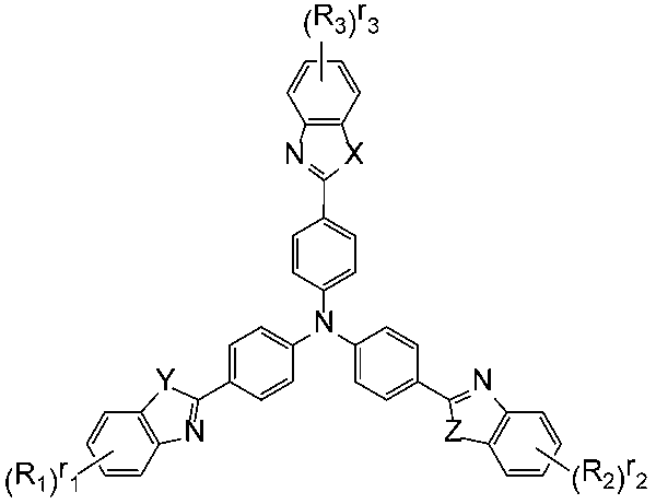
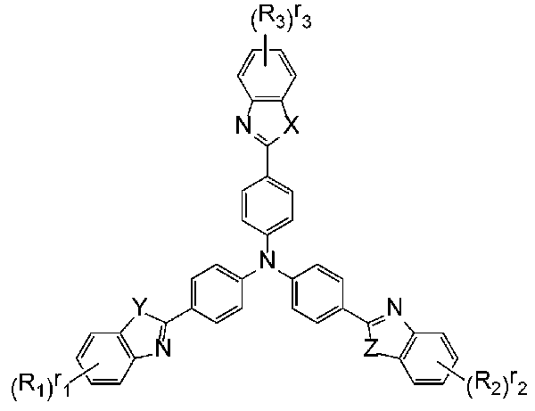
- R 1 to R 3 may be the same or different from each other, and may have a heavy hydrogen atom, a fluorine atom, a chlorine atom, a cyano group, a nitro group, and a substituent, and have 1 to 1 carbon atoms.
- Cycloalkyloxy groups substituted or unsubstituted aromatic hydrocarbon groups, substituted or unsubstituted aromatic heterocyclic groups, substituted or unsubstituted condensed polycyclic aromatic groups, or substituted or unsubstituted aryloxy groups. Representing, when a plurality of these groups are bonded to the same benzene ring, they may be bonded to each other to form a ring, and each group may be bonded to a bonded benzene ring to form a ring.
- X, Y, Z may be the same or different from each other and represent an oxygen atom or a sulfur atom
- Ar 1 to Ar 3 may be the same or different from each other, and a substituted or unsubstituted fragrance may be used. It represents a divalent group of a group hydrocarbon, a divalent group of a substituted or unsubstituted aromatic heterocycle, or a divalent group of a substituted or unsubstituted fused polycyclic aromatic.
- R 1 to r 3 may be the same as each other. It may be different and represents an integer from 0 to 4.
- any two of Ar 1 , Ar 2, and Ar 3 are divalent groups of substituted or unsubstituted aromatic hydrocarbons, as described in 1) above.
- Organic EL element any two of Ar 1 , Ar 2, and Ar 3 are divalent groups of substituted or unsubstituted aromatic hydrocarbons, as described in 1) above.
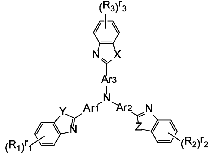
- R 1 to R 3 may be the same or different from each other, and may have a heavy hydrogen atom, a fluorine atom, a chlorine atom, a cyano group, a nitro group, and a substituent, and have 1 to 1 carbon atoms.
- Cycloalkyloxy groups substituted or unsubstituted aromatic hydrocarbon groups, substituted or unsubstituted aromatic heterocyclic groups, substituted or unsubstituted condensed polycyclic aromatic groups, or substituted or unsubstituted aryloxy groups. Representing, when a plurality of these groups are bonded to the same benzene ring, they may be bonded to each other to form a ring, and each group may be bonded to a bonded benzene ring to form a ring.
- X, Y, Z may be the same or different from each other and represent an oxygen atom or a sulfur atom
- Ar 1 to Ar 3 may be the same or different from each other, and a substituted or unsubstituted fragrance may be used. It represents a divalent group of a group hydrocarbon, a divalent group of a substituted or unsubstituted aromatic heterocycle, or a divalent group of a substituted or unsubstituted fused polycyclic aromatic.
- R 1 to r 3 may be the same as each other. It may be different and represents an integer from 0 to 4.
- Substituted or unsubstituted aromatic hydrocarbon group "substituted or unsubstituted aromatic heterocyclic group” or “substituted or non-substituted aromatic heterocyclic group” represented by R 1 to R 3 in the general formula (1) or (1a).
- aromatic hydrocarbon group “aromatic heterocyclic group” or “condensed polycyclic aromatic group” in the “substituted condensed polycyclic aromatic group” include a phenyl group, a biphenylyl group and a terphenylyl group.
- each group may be bonded to the bonded benzene ring via a single bond, substituted or unsubstituted methylene group, oxygen atom or sulfur atom to form a ring.
- Substituted aromatic hydrocarbon group "substituted aromatic heterocyclic group”, “substituted condensed polycyclic aromatic group”, “substitution” represented by R 1 to R 3 in the general formula (1) or (1a).
- a linear or branched alkyl group having 1 to 6 carbon atoms having a group "a cycloalkyl group having 5 to 10 carbon atoms having a substituent”, and "a cycloalkyl group having 2 to 6 carbon atoms having a substituent”.
- Linear or branched alkenyl group Linear or branched alkyloxy group having 1 to 6 carbon atoms having a substituent
- Cycloalkyloxy having 5 to 10 carbon atoms having a substituent Specific examples of the "substituent" in the “group” or “substituted aryloxy group” include a heavy hydrogen atom, a cyano group, a nitro group; a halogen atom such as a fluorine atom, a chlorine atom, a bromine atom and an iodine atom; , A silyl group such as a triphenylsilyl group; a linear or branched alkyl group having 1 to 6 carbon atoms such as a methyl group, an ethyl group and a propyl group; a carbon such as a methyloxy group, an ethyloxy group and a propyloxy group.
- alkenyl group such as vinyl group and allyl group
- aryloxy group such as phenyloxy group and triloxy group
- arylalkyl group such as benzyloxy group and phenethyloxy group Oxy Group
- Fragrances such as phenyl group, biphenylyl group, terphenylyl group, naphthyl group, anthracenyl group, phenanthrenyl group, fluorenyl group, spirobifluorenyl group, indenyl group, pyrenyl group, peryleneyl group, fluoranthenyl group, triphenylenyl group Group hydrocarbon group or condensed polycyclic aromatic group; pyridyl group, thienyl group, furyl group, pyrrolyl group, quinolyl group, isoquinolyl group, benzofuranyl group, benzothienyl group, indo
- substituents may be further substituted with the above-exemplified substituents. Further, these substituents may be bonded to each other via a single bond, a substituted or unsubstituted methylene group, an oxygen atom or a sulfur atom to form a ring.
- the "divalent group of the substituted or unsubstituted aromatic hydrocarbon” represented by Ar 1 to Ar 3 in the general formula (1), the "divalent group of the substituted or unsubstituted aromatic heterocycle” or The "substituted or unsubstituted fused polycyclic aromatic divalent group” can be formed by removing two hydrogen atoms from the above-mentioned "aromatic hydrocarbon", “aromatic heterocycle” or "condensed polycyclic aromatic” 2 Represents a price group.
- r 1 to r 3 may be the same or different from each other, represent an integer of 0 to 4, preferably 0 to 2, and preferably 0 to 1. Is more preferable. And it is more preferable that all of r 1 to r 3 are 0 (that is, unsubstituted).
- X, Y, and Z may be the same or different from each other and represent an oxygen atom or a sulfur atom, and any one or more of X, Y, and Z is sulfur. It is preferably an atom.
- Ar 1 to Ar 3 are preferably divalent groups of substituted or unsubstituted aromatic hydrocarbons, and are divalent groups formed by removing two hydrogen atoms from substituted or unsubstituted benzene. It is more preferably (phenylene group). Further, it is more preferable that all of Ar 1 , Ar 2 , and Ar 3 are divalent groups (phenylene groups) formed by removing two hydrogen atoms from substituted or unsubstituted benzene.
- the thickness of the capping layer is preferably in the range of 30 nm to 120 nm, and more preferably in the range of 40 nm to 80 nm.
- the refractive index of the capping layer is preferably 1.90 or more, preferably 2.00 or more, when the wavelength of light transmitted through the capping layer is within the range of 500 nm to 570 nm. More preferably.
- the capping layer may be manufactured by laminating or mixing two or more different constituent materials.
- the organic EL element of the present invention has a capping layer provided outside the transparent or translucent electrode and has a higher refractive index than the translucent electrode, so that the light extraction efficiency can be significantly improved. Made it possible to obtain. Further, by using an amine compound having a benzoazole ring structure represented by the general formula (1) or (1a) in the capping layer, a film can be formed at a temperature of 400 ° C. or lower, so that a light emitting element can be formed. It is possible to optimize the light extraction efficiency of each color by using a high-definition mask without damaging the image, and it can be suitably applied to a full-color display to display a clear and bright image with good color purity. Is now possible.
- the organic EL element of the present invention is a material for an organic EL element having a high absorption coefficient of light having a wavelength of 400 nm to 410 nm, a high refractive index, and excellent stability, durability, and light resistance of a thin film as a material for a capping layer. Compared with the conventional organic EL element, it is not affected by sunlight, maintains the color purity, and can greatly improve the light extraction efficiency. Furthermore, it has become possible to realize a highly efficient and long-life organic EL element.
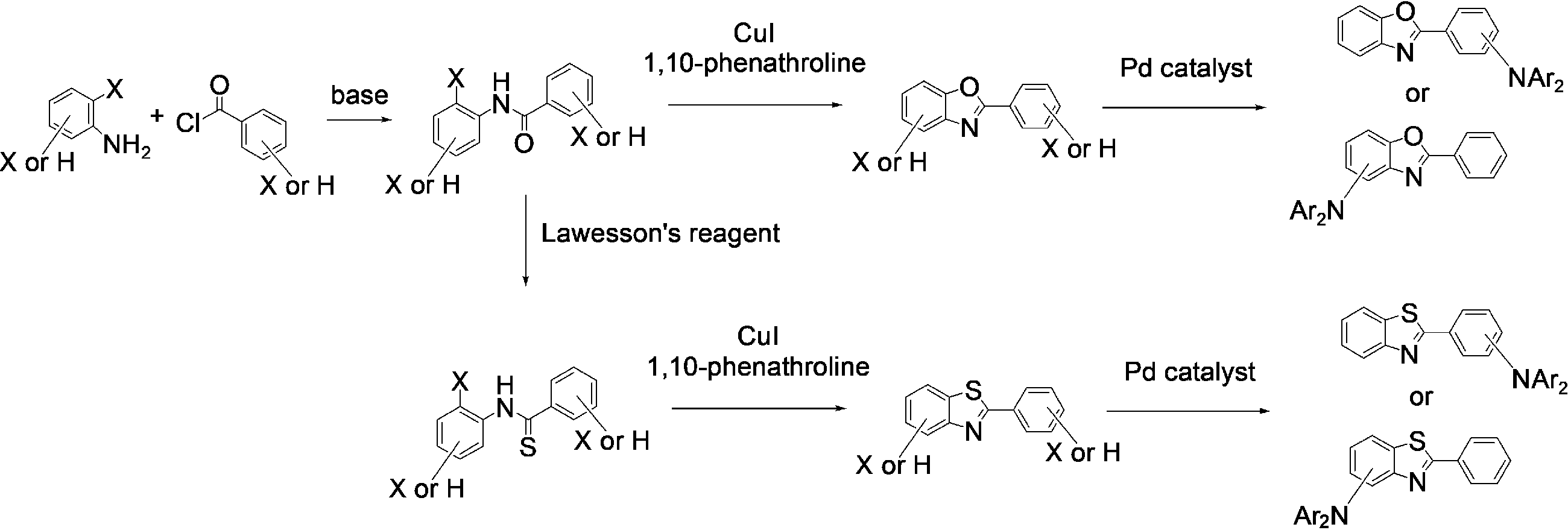
- the amine compound having the benzoazole ring structure represented by the general formula (1) or (1a) of the present invention is a novel compound, and the benzoazole derivative which is the main skeleton of these compounds is, for example, as follows. It can be synthesized by a method known per se (see, for example, Non-Patent Document 4). Further, by performing a coupling reaction between the synthesized halogenated benzoazole derivative and arylamine using a copper catalyst, a palladium catalyst, or the like, the benzoazole ring represented by the general formula (1) or (1a) of the present invention is carried out. Amine compounds having a structure can be synthesized.
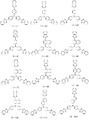
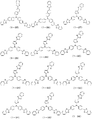
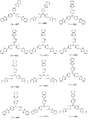
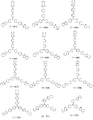
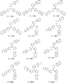
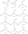
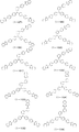
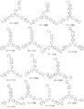
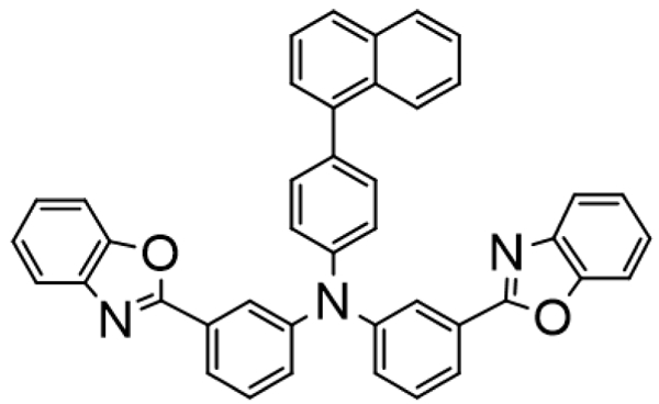
- amine compounds having a benzoazole ring structure represented by the general formula (1) or (1a), which are preferably used for the organic EL device of the present invention specific examples of the preferable compounds are shown in FIGS. 1 to 12. However, the present invention is not limited to these compounds.
- the amine compound having a benzoazole ring structure represented by the general formula (1) or (1a), which is preferably used for the organic EL element of the present invention, is purified by a column chromatograph, silica gel, activated charcoal, activated white clay or the like.
- the purification was carried out by adsorption purification by the above method, recrystallization or crystallization method using a solvent, and finally purification by a sublimation purification method or the like.
- the compounds were identified by NMR analysis. As physical property values, melting point, glass transition point (Tg), refractive index and extinction coefficient, and absorbance were measured.
- the melting point is an index of vapor deposition
- the glass transition point (Tg) is an index of stability in a thin film state
- the refractive index and extinction coefficient are indexes for improving light extraction efficiency
- the absorbance is color purity and It is an index for improving the efficiency of light extraction.
- the melting point and the glass transition point (Tg) were measured with a high-sensitivity differential scanning calorimeter (DSC3100SA, manufactured by Bruker AXS) using powder.
- the refractive index and extinction coefficient were measured by forming a thin film of 80 nm on a silicon substrate and using a spectroscopic measuring device (F10-RT-UV manufactured by Filmometrics Co., Ltd.).
- the absorbance was adjusted to a concentration of 1.0 ⁇ 10-5 mol / L in a toluene solution, and the absorbance coefficient was adjusted to a concentration of 5.0 ⁇ 10-6 mol / L and 1.0 ⁇ 10-5 mol / L in a toluene solution.
- /L,1.5 ⁇ 10 -5 mol / L, and 2.0 ⁇ 10 -5 were prepared in four concentrations of mol / L, ultraviolet-visible-near infrared spectrophotometer (manufactured by JASCO Corporation, V- It was measured using 650).
- a structure that also serves as a hole injection layer and a hole transport layer a structure that also serves as a hole transport layer and an electron blocking layer, and a positive structure.
- a configuration that also serves as a hole blocking layer and an electron transport layer, a configuration that also serves as an electron transport layer and an electron injection layer, and the like can be used.
- a laminated structure, a structure in which two capping layers are laminated, and the like are also possible.
- the total film thickness of each layer of the organic EL element is preferably about 200 nm to 750 nm, more preferably about 350 nm to 600 nm.
- the film thickness of the capping layer is, for example, preferably 30 nm to 120 nm, more preferably 40 nm to 80 nm. In this case, good light extraction efficiency can be obtained.
- the film thickness of the capping layer can be appropriately changed according to the type of light emitting material used for the light emitting element, the thickness of each layer of the organic EL element other than the capping layer, and the like.
- an electrode material having a large work function such as ITO or gold is used.
- an arylamine compound having a structure in which three or more triphenylamine structures are linked in a molecule by a divalent group containing no single bond or hetero atom for example, Starburst.
- Materials such as triphenylamine derivatives of type, various triphenylamine tetramers; porphyrin compounds typified by copper phthalocyanine; acceptor heterocyclic compounds such as hexacyanoazatriphenylene; coated polymer materials, etc. Can be used. These may be formed alone, or may be used as a single layer formed by mixing with other materials, and the layers formed alone, the layers formed by mixing, or the layers formed by mixing. It may be a laminated structure of a layer formed by mixing with a layer formed alone. These materials can be thin-film formed by a known method such as a spin coating method or an inkjet method in addition to the vapor deposition method.
- an arylamine compound having a structure in which three or more triphenylamine structures are linked in a molecule with a single bond or a divalent group containing no hetero atom for example, various triphenylamine trimerics or tetramers. It is also preferable to use.
- a material usually used for the layer is further P-doped with trisbromophenylamine hexachloroantimony, a radialene derivative (see, for example, Patent Document 3) or the like.
- a polymer compound having the structure of a benzidine derivative such as TPD in its partial structure can be used.
- TCTA 4,4', 4''-tri (N-carbazolyl) triphenylamine
- TCTA 9,9-bis [4- (carbazole-9-yl) phenyl)
- Carbazole derivatives such as fluorene, 1,3-bis (carbazole-9-yl) benzene (mCP), 2,2-bis (4-carbazole-9-yl-phenyl) adamantan (Ad-Cz); 9- [4 -(Carbazole-9-yl) phenyl] -9- [4- (triphenylsilyl) phenyl] -9H-A compound having a triphenylsilyl group represented by fluorene and a triarylamine structure, etc.
- Fluorene compounds can be used. These may be formed alone, or may be used as a single layer formed by mixing with other materials, and the layers formed alone, the layers formed by mixing, or the layers formed by mixing, or It may be a laminated structure of a layer formed by mixing with a layer formed alone. These materials can be thin-film formed by a known method such as a spin coating method or an inkjet method in addition to the vapor deposition method.
- the light emitting layer of the organic EL element of the present invention in addition to metal complexes of quinolinol derivatives such as Alq 3 , various metal complexes, anthracene derivatives, bisstyrylbenzene derivatives, pyrene derivatives, oxazole derivatives, polyparaphenylene vinylene derivatives, etc. Can be used. Further, the light emitting layer may be composed of a host material and a dopant material, and an anthracene derivative is preferably used as the host material. In addition, various metal complexes, bisstyrylbenzene derivatives, pyrene derivatives, oxazole derivatives, and polyparas are used.
- a phenylene vinylene derivative a heterocyclic compound having an indole ring as a partial structure of the fused ring, a heterocyclic compound having a carbazole ring as a partial structure of the fused ring, a carbazole derivative, a thiazole derivative, a benzimidazole derivative, a polydialkylfluorene derivative, or the like.
- a dopant material quinacridone, coumarin, rubrene, perylene and derivatives thereof, benzopyran derivative, rhodamine derivative, aminostyryl derivative and the like can be used, and it is particularly preferable to use a green light emitting material.
- These may be formed alone, or may be used as a single layer formed by mixing with other materials, and the layers formed alone, the layers formed by mixing, or the layers formed by mixing. It may be a laminated structure of a layer formed by mixing with a layer formed alone.
- a phosphorescent light emitter As the phosphorescent body, a phosphorescent body of a metal complex such as iridium or platinum can be used. A green phosphorescent body such as Ir (ppy) 3 , a blue phosphorescent light emitter such as Firpic or Fir6, a red phosphorescent light emitter such as Btp 2 Ir (acac), etc. are used, and a green phosphorescent light emitter is used. Is particularly preferable.
- a carbazole derivative such as 4,4'-di (N-carbazolyl) biphenyl (CBP), TCTA, or mCP can be used as the host material for hole injection / transportability.
- CBP 4,4'-di (N-carbazolyl) biphenyl
- TCTA TCTA
- mCP mCP
- an electron transporting host material p-bis (triphenylsilyl) benzene (UGH2) and 2,2', 2''-(1,3,5-phenylene) -tris (1-phenyl-1H-benzimidazole) ) (TPBI) or the like can be used, and a high-performance organic EL element can be manufactured.
- Doping of the phosphorescent luminescent material to the host material is preferably done by co-depositing in the range of 1 to 30% by weight with respect to the entire light emitting layer in order to avoid concentration quenching.
- Non-Patent Document 7 a material that emits delayed fluorescence such as a CDCB derivative such as PIC-TRZ, CC2TA, PXZ-TRZ, 4CzIPN as a light emitting material.
- a material that emits delayed fluorescence such as a CDCB derivative such as PIC-TRZ, CC2TA, PXZ-TRZ, 4CzIPN
- These materials can be thin-film formed by a known method such as a spin coating method or an inkjet method in addition to a thin film deposition method.
- These may be formed alone, or may be used as a single layer formed by mixing with other materials, and the layers formed alone, the layers formed by mixing, or the layers formed by mixing, or It may be a laminated structure of a layer formed by mixing with a layer formed alone.
- These materials can be thin-film formed by a known method such as a spin coating method or an inkjet method in addition to the vapor deposition method.
- the electron transport layer of the organic EL element of the present invention in addition to metal complexes of quinolinol derivatives such as Alq 3 and BAlq, various metal complexes, triazole derivatives, triazine derivatives, pyrimidine derivatives, oxadiazole derivatives, pyridine derivatives, and benz Imidazole derivatives, benzoazole derivatives, thiadiazol derivatives, anthracene derivatives, carbodiimide derivatives, quinoxalin derivatives, pyridoindole derivatives, phenanthroline derivatives, silol derivatives and the like can be used.
- quinolinol derivatives such as Alq 3 and BAlq
- These may be formed alone, or may be used as a single layer formed by mixing with other materials, and the layers formed alone, the layers formed by mixing, or the layers formed by mixing, or It may be a laminated structure of a layer formed by mixing with a layer formed alone.
- These materials can be thin-film formed by a known method such as a spin coating method or an inkjet method in addition to the vapor deposition method.
- alkali metal salts such as lithium fluoride and cesium fluoride
- alkaline earth metal salts such as magnesium fluoride
- metal complexes of quinolinol derivatives such as lithium quinolinol, aluminum oxide and the like.
- Metal oxides or metals such as itterbium (Yb), samarium (Sm), calcium (Ca), strontium (Sr), cesium (Cs) can be used, but in the preferred selection of electron transport layer and cathode. , This can be omitted.
- a material usually used for the layer which is further N-doped with a metal such as cesium, can be used.
- an electrode material having a low work function such as aluminum, an alloy having a lower work function such as a magnesium silver alloy, a magnesium calcium alloy, a magnesium indium alloy, and an aluminum magnesium alloy, ITO, etc. IZO or the like is used as an electrode material.
- these may be formed alone, or may be used as a single layer formed by mixing different materials, or layers formed independently, layers formed by mixing, or layers formed by mixing. It may be a laminated structure of a layer formed by mixing with a layer formed alone.
- these materials can be thin-film formed by a known method such as a spin coating method or an inkjet method.
- the present invention is not limited to this, and the organic EL element having a bottom emission structure or a dual emission structure that emits light from both the upper part and the bottom portion. The same can be applied to an organic EL element. In these cases, the electrodes in the direction in which the light is taken out from the light emitting element need to be transparent or translucent.
- the refractive index of the material constituting the capping layer is larger than the refractive index of the adjacent electrodes. That is, the capping layer improves the light extraction efficiency of the organic EL element, but the effect is that the larger the reflectance at the interface between the capping layer and the material in contact with the capping layer, the greater the effect of light interference. It is effective for. Therefore, the refractive index of the material constituting the capping layer is preferably larger than the refractive index of the adjacent electrodes, and the refractive index may be 1.90 or more, but more preferably 2.00 or more.
- Tg melting point and glass transition point (Tg) of an amine compound having a benzoazole ring structure represented by the general formula (1) or (1a) are measured by a high-sensitivity differential scanning calorimeter (DSC3100SA, manufactured by Bruker AXS). did.
- Melting point glass transition point (Tg) Compound of Example 1 277 °C 126 °C Compound of Example 2 274 ° C 123 ° C Compound of Example 3 270 ° C 119 ° C
- the amine compound having a benzoazole ring structure represented by the general formula (1) or (1a) has a glass transition point of 100 ° C. or higher, indicating that the thin film state is stable.
- a vapor-deposited film having a film thickness of 80 nm was prepared on a silicon substrate using an amine compound having a benzoazole ring structure represented by the general formula (1) or (1a), and a spectroscopic measuring device (manufactured by Filmometry, F10-) was prepared.
- RT-UV was used to measure the refractive index n at wavelengths 400 nm, 410 nm, 500 nm, and 570 nm and the extinction coefficient k at wavelengths 400 nm and 410 nm.
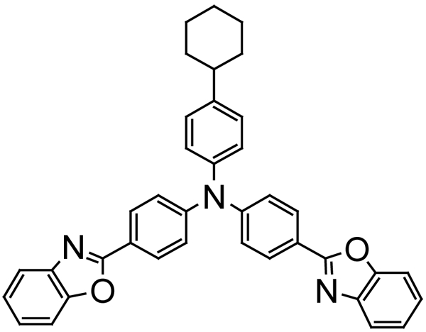
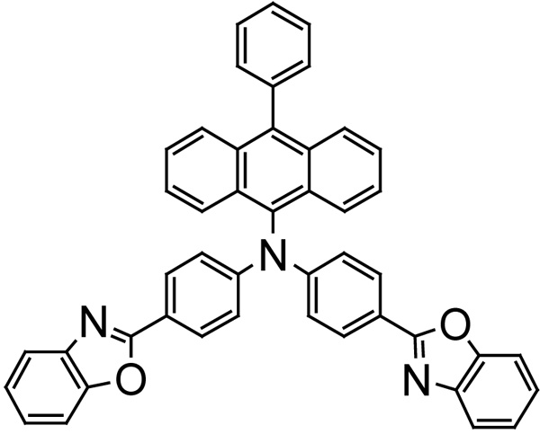
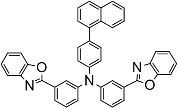
- comparative compounds (2-1), (2-2), (2-3) and (2-4) having the following structural formulas were also measured (see, for example, Patent Document 4). The measurement results are summarized in Table 1.
- the compound of the present invention has a refractive index of 1.90 or more in the wavelength range of 500 nm to 570 nm, and the comparative compounds (2-1), (2-2), (2-3) and (2-). 4) It has a larger refractive index. This indicates that improvement in light extraction efficiency in the organic EL element can be expected. Further, the extinction coefficient at wavelengths of 400 nm to 410 nm is less than 0.5 for the comparative compounds (2-1), (2-2), (2-3) and (2-4), whereas the extinction coefficient of the present invention is less than 0.5. The compound has a larger value. This indicates that the light having a wavelength of 400 nm to 410 nm of sunlight is well absorbed and does not affect the material inside the device.
- the concentration was adjusted to 1.0 ⁇ 10-5 mol / L in a toluene solution, and the absorbance at wavelengths of 400 nm and 410 nm was measured with an ultraviolet-visible near-infrared spectrophotometer (JASCO Corporation, V-650). Was measured using.
- the extinction coefficient is 5.0 ⁇ 10 -6 mol / L, 1.0 ⁇ 10 -5 mol / L, 1.5 ⁇ 10 -5 mol / L, and 2.0 ⁇ 10 -5 mol / L in a toluene solution.
- the absorbance at wavelengths of 400 nm to 410 nm is less than 0.7 for the comparative compounds (2-1), (2-2), (2-3) and (2-4), whereas the present invention.
- the compound has a large value of 0.7 or more, which indicates that it absorbs light having a wavelength of 400 nm to 410 nm of sunlight well.
- the compound of the present invention has a large value in terms of absorption coefficient as compared with the comparative compounds (2-1), (2-2), (2-3) and (2-4), and has the same concentration. It shows that the light is well absorbed under the conditions, and that the thinner the film thickness is, the better the light is absorbed, indicating that the material has excellent light resistance.
- the organic EL element has a hole injection layer 3, a first hole transport layer 4, and a second hole on a glass substrate 1 on which a reflective ITO electrode is previously formed as a metal anode 2.
- the transport layer 5, the light emitting layer 6, the electron transport layer 7, the electron injection layer 8, the cathode 9, and the capping layer 10 were vapor-deposited in this order.
- an ITO having a film thickness of 50 nm, a silver alloy reflective film having a film thickness of 100 nm, and an ITO having a film thickness of 5 nm are formed in this order, and ultrasonically washed in isopropyl alcohol.
- isopropyl alcohol was carried out for 20 minutes, and then dried on a hot plate heated to 250 ° C. for 10 minutes.
- the glass substrate with ITO was mounted in a vacuum vapor deposition machine and the pressure was reduced to 0.001 Pa or less.
- an electron acceptor (Acceptor-1) having the following structural formula and a compound (3-1) having the following structural formula are used, and the vapor deposition rate ratio is Acceptor-1: compound.
- a compound (3-1) having the following structural formula was formed as the first hole transport layer 4 so as to have a film thickness of 70 nm.
- a compound (3-2) having the following structural formula was formed as the second hole transport layer 5 on the first hole transport layer 4 so as to have a film thickness of 10 nm.
- a compound (3-3) having the following structural formula and a compound (3-4) having the following structural formula are used as the light emitting layer 6, and the vapor deposition rate ratio is compound (3-3) :.
- a compound (3-5) having the following structural formula and a compound (3-6) having the following structural formula are used as the electron transport layer 7, and the vapor deposition rate ratio is compound (3-5): compound (3).
- Lithium fluoride was formed on the electron transport layer 7 as an electron injection layer 8 so as to have a film thickness of 1 nm.
- a magnesium-silver alloy was formed on the electron injection layer 8 as a cathode 9 so as to have a film thickness of 12 nm.
- the compound (1-1) of Example 1 was formed as the capping layer 10 so as to have a film thickness of 60 nm.
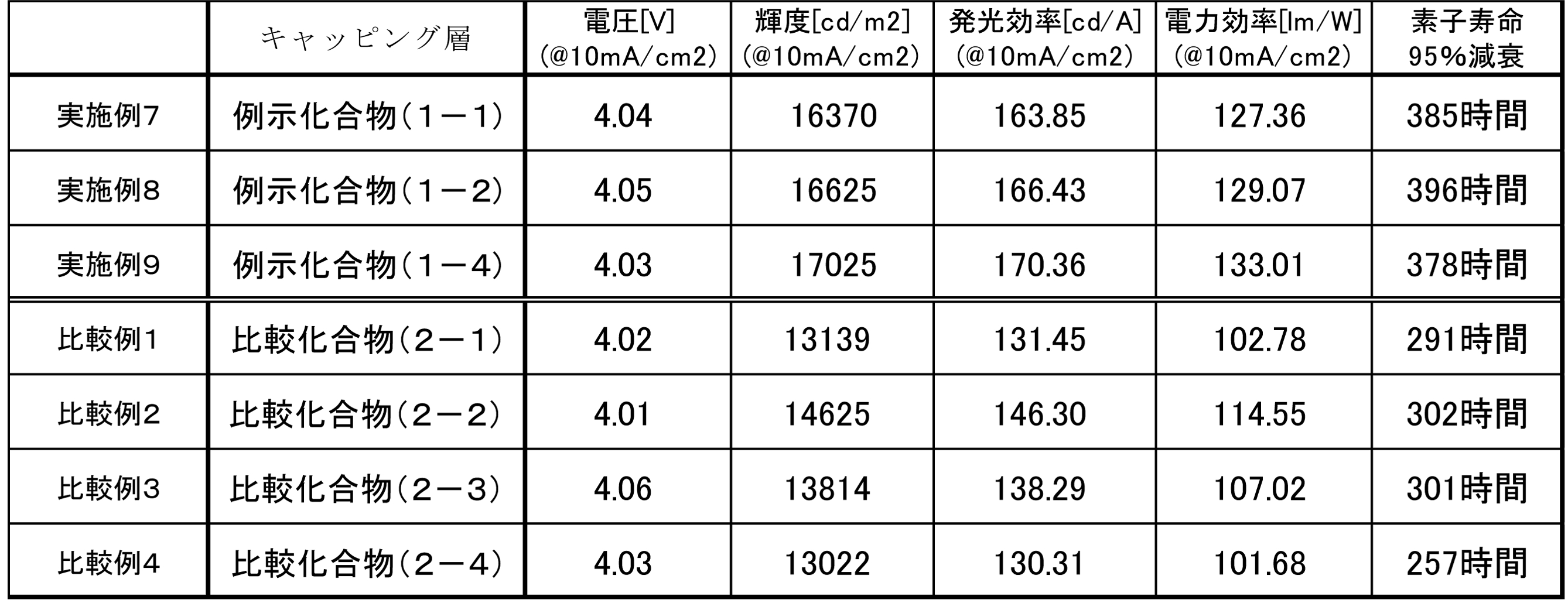
- Table 3 summarizes the measurement results of the light emission characteristics when a DC voltage is applied to the produced organic EL element.
- Example 7 an organic EL device was produced under the same conditions except that the compound (1-2) of Example 2 was used instead of the compound (1-1) of Example 1 as the material of the capping layer 10. ..
- the characteristics of the produced organic EL device were measured in the air at room temperature. Table 3 summarizes the measurement results of the light emission characteristics when a DC voltage is applied to the produced organic EL element.
- Example 7 an organic EL device was produced under the same conditions except that the compound (1-4) of Example 3 was used instead of the compound (1-1) of Example 1 as the material of the capping layer 10. ..
- the characteristics of the produced organic EL device were measured in the air at room temperature. Table 3 summarizes the measurement results of the light emission characteristics when a DC voltage is applied to the produced organic EL element.
- Example 7 For comparison, under the same conditions, except that the comparative compound (2-1) having the following structural formula was used in place of the compound (1-1) of Example 1 as the material of the capping layer 10 in Example 7. An organic EL element was manufactured. The characteristics of the produced organic EL device were measured in the air at room temperature. Table 3 summarizes the measurement results of the light emission characteristics when a DC voltage is applied to the produced organic EL element.
- Example 7 For comparison, under the same conditions, except that the comparative compound (2-2) having the following structural formula was used in place of the compound (1-1) of Example 1 as the material of the capping layer 10 in Example 7. An organic EL element was manufactured. The characteristics of the produced organic EL device were measured in the air at room temperature. Table 3 summarizes the measurement results of the light emission characteristics when a DC voltage is applied to the produced organic EL element.
- Example 7 For comparison, under the same conditions, except that the comparative compound (2-3) having the following structural formula was used in place of the compound (1-1) of Example 1 as the material of the capping layer 10 in Example 7. An organic EL element was manufactured. The characteristics of the produced organic EL device were measured in the air at room temperature. Table 3 summarizes the measurement results of the light emission characteristics when a DC voltage is applied to the produced organic EL element.
- Example 7 For comparison, under the same conditions, except that the comparative compound (2-4) having the following structural formula was used in place of the compound (1-1) of Example 1 as the material of the capping layer 10 in Example 7. An organic EL element was manufactured. The characteristics of the produced organic EL device were measured in the air at room temperature. Table 3 summarizes the measurement results of the light emission characteristics when a DC voltage is applied to the produced organic EL element.
- Table 3 shows the results of measuring the device life using the organic EL devices manufactured in Examples 7 to 9 and Comparative Examples 1 to 4.
- the device life was measured as the time (95% attenuation) until the element life was attenuated to 95% when the initial brightness was 100% when the constant current drive was performed at 10 mA / cm 2.
- the drive voltage at a current density of 10 mA / cm at 2 o'clock is almost the same in the elements of Comparative Examples 1 to 4 and the elements of Examples 7 to 9, whereas the brightness, luminous efficiency, and power efficiency are almost the same.
- the elements of Examples 7 to 9 were improved as compared with the elements of Comparative Examples 1 to 4. This indicates that the light extraction efficiency can be significantly improved by including a material having a high refractive index and preferably used for the organic EL device of the present invention in the capping layer.
- the amine compound having a benzoazole ring structure represented by the general formula (1) which is preferably used for the organic EL device of the present invention, has a high absorption coefficient of light having a wavelength of 400 nm to 410 nm and a refractive index. It is excellent as a compound for an organic EL device because it has a high light extraction efficiency, can greatly improve the light extraction efficiency, and has a stable thin film state. By producing an organic EL device using the compound, high efficiency can be obtained, and durability and light resistance are improved so as to absorb sunlight and not affect the material inside the device. be able to. Further, by using the compound having no absorption in each of the wavelength regions of blue, green and red, it is particularly suitable when it is desired to display a clear and bright image with good color purity. For example, it has become possible to develop it for home appliances and lighting applications.
Landscapes
- Physics & Mathematics (AREA)
- Optics & Photonics (AREA)
- Spectroscopy & Molecular Physics (AREA)
- Chemical & Material Sciences (AREA)
- Engineering & Computer Science (AREA)
- Materials Engineering (AREA)
- Electroluminescent Light Sources (AREA)
Abstract
Description

(1)
(式中、R1~R3は相互に同一でも異なっていてもよく、重水素原子、フッ素原子、塩素原子、シアノ基、ニトロ基、置換基を有していてもよい炭素原子数1ないし6の直鎖状もしくは分岐状のアルキル基、置換基を有していてもよい炭素原子数5ないし10のシクロアルキル基、置換基を有していてもよい炭素原子数2ないし6の直鎖状もしくは分岐状のアルケニル基、置換基を有していてもよい炭素原子数1ないし6の直鎖状もしくは分岐状のアルキルオキシ基、置換基を有していてもよい炭素原子数5ないし10のシクロアルキルオキシ基、置換もしくは無置換の芳香族炭化水素基、置換もしくは無置換の芳香族複素環基、置換もしくは無置換の縮合多環芳香族基、または置換もしくは無置換のアリールオキシ基を表し、これらの基が同一のベンゼン環に複数個結合している場合は互いに結合して環を形成していてもよく、それぞれの基が結合しているベンゼン環と結合して環を形成してもよい。X、Y、Zは相互に同一でも異なっていてもよく、酸素原子または硫黄原子を表し、Ar1~Ar3は相互に同一でも異なっていてもよく、置換もしくは無置換の芳香族炭化水素の2価基、置換もしくは無置換の芳香族複素環の2価基、または置換もしくは無置換の縮合多環芳香族の2価基を表す。r1~r3は相互に同一でも異なっていてもよく、0~4の整数を表す。)
(1a)
(式中、R1~R3、X、Y、Z、r1~r3は前記一般式(1)で定義する通りである。)
(1)
(式中、R1~R3は相互に同一でも異なっていてもよく、重水素原子、フッ素原子、塩素原子、シアノ基、ニトロ基、置換基を有していてもよい炭素原子数1ないし6の直鎖状もしくは分岐状のアルキル基、置換基を有していてもよい炭素原子数5ないし10のシクロアルキル基、置換基を有していてもよい炭素原子数2ないし6の直鎖状もしくは分岐状のアルケニル基、置換基を有していてもよい炭素原子数1ないし6の直鎖状もしくは分岐状のアルキルオキシ基、置換基を有していてもよい炭素原子数5ないし10のシクロアルキルオキシ基、置換もしくは無置換の芳香族炭化水素基、置換もしくは無置換の芳香族複素環基、置換もしくは無置換の縮合多環芳香族基、または置換もしくは無置換のアリールオキシ基を表し、これらの基が同一のベンゼン環に複数個結合している場合は互いに結合して環を形成していてもよく、それぞれの基が結合しているベンゼン環と結合して環を形成してもよい。X、Y、Zは相互に同一でも異なっていてもよく、酸素原子または硫黄原子を表し、Ar1~Ar3は相互に同一でも異なっていてもよく、置換もしくは無置換の芳香族炭化水素の2価基、置換もしくは無置換の芳香族複素環の2価基、または置換もしくは無置換の縮合多環芳香族の2価基を表す。r1~r3は相互に同一でも異なっていてもよく、0~4の整数を表す。)

(式中、R1~R3、X、Y、Z、r1~r3は前記一般式(1)で定義する通りである。)
また、これらの基が同一のベンゼン環に複数個結合している場合は、単結合、置換もしくは無置換のメチレン基、酸素原子または硫黄原子を介して互いに結合して環を形成していてもよく、それぞれの基が結合しているベンゼン環と単結合、置換もしくは無置換のメチレン基、酸素原子または硫黄原子を介して結合して環を形成してもよい。
また、これらの基が同一のベンゼン環に複数個結合している場合は、単結合、置換もしくは無置換のメチレン基、酸素原子または硫黄原子を介して互いに結合して環を形成していてもよく、それぞれの基が結合しているベンゼン環と単結合、置換もしくは無置換のメチレン基、酸素原子または硫黄原子を介して結合して環を形成してもよい。
また、これらの置換基どうしが単結合、置換もしくは無置換のメチレン基、酸素原子または硫黄原子を介して互いに結合して環を形成していてもよい。
一般式(1)または(1a)において、X、Y、およびZは相互に同一でも異なっていてもよく、酸素原子または硫黄原子を表し、X、Y、およびZのいずれか1つ以上が硫黄原子であることが好ましい。
一般式(1)において、Ar1~Ar3は置換もしくは無置換の芳香族炭化水素の2価基であることが好ましく、置換もしくは無置換のベンゼンから水素原子を2個取り除いてできる2価基(フェニレン基)であることがより好ましい。そして、Ar1、Ar2、およびAr3の全てが置換もしくは無置換のベンゼンから水素原子を2個取り除いてできる2価基(フェニレン基)であることがさらに好ましい。
また、ハロゲン化ベンゾアゾール誘導体をボロン酸誘導体、またはボロン酸エステル誘導体に誘導した後、ハロゲン化アリールアミンとのカップリング反応を行うことにより、同様に本発明の前記一般式(1)または(1a)で表されるベンゾアゾール環構造を有するアミン化合物を合成することができる(例えば、非特許文献5および非特許文献6参照)。
反応容器にビス[4-(ベンゾオキサゾール-2-イル)-フェニル]アミン:12.3g、2-(4-ブロモフェニル)ベンゾオキサゾール:9.2g、tert-ブトキシナトリウム:4.4g、トルエン:130mlを加え、30分間超音波を照射しながら窒素ガスを通気した。酢酸パラジウム(II):0.1g、トリ-(tert-ブチル)ホスフィンの50%(w/v)トルエン溶液:0.3gを加えて加熱還流下、一晩撹拌した。放冷後、80℃で分散洗浄を行い、不溶物を濾別して得られた濾液を濃縮して粗製物を得た。粗製物をトルエン/アセトン混合溶媒を用いた晶析精製によって析出した固体を採取し、例示化合物(1-1)の黄色粉体:10.0g(収率54.9%)を得た。

(1-1)
1H-NMR(CDCl3)で以下の24個の水素のシグナルを検出した。
δ(ppm)=8.25-8.21(6H)、7.82-7.76(3H)、7.63-7.57(3H)、7.41-7.32(12H)。
反応容器にビス[4-(ベンゾオキサゾール-2-イル)-フェニル]アミン:12.3g、2-(4-ブロモフェニル)ベンゾチアゾール:9.7g、tert-ブトキシナトリウム:4.4g、トルエン:130mlを加え、30分間超音波を照射しながら窒素ガスを通気した。酢酸パラジウム(II):0.1g、トリ-(tert-ブチル)ホスフィンの50%(w/v)トルエン溶液:0.3gを加えて加熱還流下、一晩撹拌した。放冷後、80℃で分散洗浄を行い、不溶物を濾別して得られた濾液を濃縮して粗製物を得た。粗製物をトルエン/アセトン混合溶媒を用いた晶析精製によって析出した固体を採取し、例示化合物(1-2)の黄色粉体:14.5g(収率77.5%)を得た。

(1-2)
1H-NMR(CDCl3)で以下の24個の水素のシグナルを検出した。
δ(ppm)=8.24-8.21(4H)、8.09-8.06(3H)、7.92-7.89(1H)、7.80-7.77(2H)、7.60-7.58(2H)、7.51(1H)、7.41-7.29(11H)。
反応容器に2-(4-アミノフェニル)ベンゾチアゾール:6.0g、2-(4-ブロモフェニル)ベンゾチアゾール:16.2g、tert-ブトキシナトリウム:7.6g、トルエン:150mlを加え、30分間超音波を照射しながら窒素ガスを通気した。トリス(ジベンジリデンアセトン)パラジウム(0):0.2g、トリ-(tert-ブチル)ホスフィンの50%(w/v)トルエン溶液:0.2gを加えて加熱還流下、一晩撹拌した。放冷後、80℃で分散洗浄を行い、不溶物を濾別して得られた濾液を濃縮して粗製物を得た。粗製物をトルエン/アセトン混合溶媒を用いた晶析精製によって析出した固体を採取し、例示化合物(1-4)の黄色粉体:10.2g(収率59.6%)を得た。

(1-4)
1H-NMR(CDCl3)で以下の24個の水素のシグナルを検出した。
δ(ppm)=8.10-8.05(9H)、7.92-7.90(3H)、7.54-7.48(3H)、7.42-7.37(3H)、7.31-7.27(6H)。
融点 ガラス転移点(Tg)
実施例1の化合物 277℃ 126℃
実施例2の化合物 274℃ 123℃
実施例3の化合物 270℃ 119℃

(2-1)

(2-2)
(2-3)
(2-4)

また、波長400nmから410nmにおける消衰係数が比較化合物(2-1)、(2-2)、(2-3)および(2-4)は0.5未満であるのに対し、本発明の化合物はより大きな値を有している。このことは太陽光の波長400nmから410nmの光をよく吸光し素子内部の材料に影響を与えないことを示すものである。

作製した有機EL素子に直流電圧を印加した発光特性の測定結果を表3にまとめて示した。

(Acceptor-1)
(3-1)

(3-2)

(3-3)

(3-4)
(3-5)
(3-6)

(1-1)
作製した有機EL素子に直流電圧を印加したときの発光特性の測定結果を表3にまとめて示した。

(1-2)
作製した有機EL素子に直流電圧を印加したときの発光特性の測定結果を表3にまとめて示した。

(1-4)
[比較例1]
作製した有機EL素子に直流電圧を印加した発光特性の測定結果を表3にまとめて示した。
(2-1)
[比較例2]
作製した有機EL素子に直流電圧を印加した発光特性の測定結果を表3にまとめて示した。
(2-2)
[比較例3]
作製した有機EL素子に直流電圧を印加した発光特性の測定結果を表3にまとめて示した。
(2-3)
[比較例4]
作製した有機EL素子に直流電圧を印加した発光特性の測定結果を表3にまとめて示した。

(2-4)
2 金属陽極
3 正孔注入層
4 第一正孔輸送層
5 第二正孔輸送層
6 発光層
7 電子輸送層
8 電子注入層
9 陰極
10 キャッピング層
Claims (5)
- 少なくとも陽極電極、正孔輸送層、発光層、電子輸送層、陰極電極およびキャッピング層をこの順に有する有機エレクトロルミネッセンス素子において、前記キャッピング層が波長500nmから570nmにおける屈折率が1.90以上であって、かつ、下記一般式(1)で表されるベンゾアゾール環構造を有するアミン化合物を含む有機エレクトロルミネッセンス素子。

(1)
(式中、R1~R3は相互に同一でも異なっていてもよく、重水素原子、フッ素原子、塩素原子、シアノ基、ニトロ基、置換基を有していてもよい炭素原子数1ないし6の直鎖状もしくは分岐状のアルキル基、置換基を有していてもよい炭素原子数5ないし10のシクロアルキル基、置換基を有していてもよい炭素原子数2ないし6の直鎖状もしくは分岐状のアルケニル基、置換基を有していてもよい炭素原子数1ないし6の直鎖状もしくは分岐状のアルキルオキシ基、置換基を有していてもよい炭素原子数5ないし10のシクロアルキルオキシ基、置換もしくは無置換の芳香族炭化水素基、置換もしくは無置換の芳香族複素環基、置換もしくは無置換の縮合多環芳香族基、または置換もしくは無置換のアリールオキシ基を表し、これらの基が同一のベンゼン環に複数個結合している場合は互いに結合して環を形成していてもよく、それぞれの基が結合しているベンゼン環と結合して環を形成してもよい。X、Y、Zは相互に同一でも異なっていてもよく、酸素原子または硫黄原子を表し、Ar1~Ar3は相互に同一でも異なっていてもよく、置換もしくは無置換の芳香族炭化水素の2価基、置換もしくは無置換の芳香族複素環の2価基、または置換もしくは無置換の縮合多環芳香族の2価基を表す。r1~r3は相互に同一でも異なっていてもよく、0~4の整数を表す。) - 前記ベンゾアゾール環構造を有するアミン化合物が下記一般式(1a)で表されることを特徴とする、請求項1記載の有機エレクトロルミネッセンス素子。

(1a)
(式中、R1~R3、X、Y、Z、r1~r3は前記一般式(1)で定義する通りである。) - 前記一般式(1)または一般式(1a)において、r1~r3のすべてが0であることを特徴とする、請求項1または2記載の有機エレクトロルミネッセンス素子。
- 前記キャッピング層の厚さが、30nm~120nmの範囲内である、請求項1記載の有機エレクトロルミネッセンス素子。
- 波長500nmから570nmにおける屈折率が1.90以上であって、かつ、下記一般式(1)または一般式(1a)で表されるベンゾアゾール環構造を有するアミン化合物を有機エレクトロルミネッセンス素子のキャッピング層に用いる方法。

(1)
(式中、R1~R3は相互に同一でも異なっていてもよく、重水素原子、フッ素原子、塩素原子、シアノ基、ニトロ基、置換基を有していてもよい炭素原子数1ないし6の直鎖状もしくは分岐状のアルキル基、置換基を有していてもよい炭素原子数5ないし10のシクロアルキル基、置換基を有していてもよい炭素原子数2ないし6の直鎖状もしくは分岐状のアルケニル基、置換基を有していてもよい炭素原子数1ないし6の直鎖状もしくは分岐状のアルキルオキシ基、置換基を有していてもよい炭素原子数5ないし10のシクロアルキルオキシ基、置換もしくは無置換の芳香族炭化水素基、置換もしくは無置換の芳香族複素環基、置換もしくは無置換の縮合多環芳香族基、または置換もしくは無置換のアリールオキシ基を表し、これらの基が同一のベンゼン環に複数個結合している場合は互いに結合して環を形成していてもよく、それぞれの基が結合しているベンゼン環と結合して環を形成してもよい。X、Y、Zは相互に同一でも異なっていてもよく、酸素原子または硫黄原子を表し、Ar1~Ar3は相互に同一でも異なっていてもよく、置換もしくは無置換の芳香族炭化水素の2価基、置換もしくは無置換の芳香族複素環の2価基、または置換もしくは無置換の縮合多環芳香族の2価基を表す。r1~r3は相互に同一でも異なっていてもよく、0~4の整数を表す。)
(1a)
(式中、R1~R3、X、Y、Z、r1~r3は前記一般式(1)で定義する通りである。)
Priority Applications (5)
| Application Number | Priority Date | Filing Date | Title |
|---|---|---|---|
| EP20912722.4A EP4089156A4 (en) | 2020-01-08 | 2020-12-21 | Organic electroluminescence element |
| US17/791,279 US20230354629A1 (en) | 2020-01-08 | 2020-12-21 | Organic electroluminescent device |
| CN202080092185.7A CN114946273B (zh) | 2020-01-08 | 2020-12-21 | 有机电致发光元件 |
| JP2021569814A JP7794640B2 (ja) | 2020-01-08 | 2020-12-21 | 有機エレクトロルミネッセンス素子 |
| KR1020227022229A KR20220124697A (ko) | 2020-01-08 | 2020-12-21 | 유기 일렉트로루미네센스 소자 |
Applications Claiming Priority (2)
| Application Number | Priority Date | Filing Date | Title |
|---|---|---|---|
| JP2020001564 | 2020-01-08 | ||
| JP2020-001564 | 2020-01-08 |
Publications (1)
| Publication Number | Publication Date |
|---|---|
| WO2021140896A1 true WO2021140896A1 (ja) | 2021-07-15 |
Family
ID=76788601
Family Applications (1)
| Application Number | Title | Priority Date | Filing Date |
|---|---|---|---|
| PCT/JP2020/047680 Ceased WO2021140896A1 (ja) | 2020-01-08 | 2020-12-21 | 有機エレクトロルミネッセンス素子 |
Country Status (7)
| Country | Link |
|---|---|
| US (1) | US20230354629A1 (ja) |
| EP (1) | EP4089156A4 (ja) |
| JP (1) | JP7794640B2 (ja) |
| KR (1) | KR20220124697A (ja) |
| CN (1) | CN114946273B (ja) |
| TW (1) | TW202136223A (ja) |
| WO (1) | WO2021140896A1 (ja) |
Cited By (4)
| Publication number | Priority date | Publication date | Assignee | Title |
|---|---|---|---|---|
| EP4210450A3 (en) * | 2022-01-10 | 2023-07-26 | Samsung Display Co., Ltd. | Light-emitting device and electronic apparatus including the same |
| EP4210453A3 (en) * | 2022-01-10 | 2023-10-11 | Samsung Display Co., Ltd. | Light-emitting device and electronic apparatus including the same |
| WO2024010050A1 (ja) | 2022-07-07 | 2024-01-11 | 保土谷化学工業株式会社 | アミン化合物、並びに、それを含有する有機エレクトロルミネッセンス素子、電子機器、及び電子素子 |
| WO2024237322A1 (ja) | 2023-05-18 | 2024-11-21 | 保土谷化学工業株式会社 | 芳香族化合物、有機エレクトロルミネッセンス素子および電子機器 |
Families Citing this family (1)
| Publication number | Priority date | Publication date | Assignee | Title |
|---|---|---|---|---|
| EP3929193B1 (en) * | 2019-02-22 | 2024-10-23 | Hodogaya Chemical Co., Ltd. | Organic electroluminescent element comprising a capping layer with an arylamine compound having benzoazole ring structure |
Citations (8)
| Publication number | Priority date | Publication date | Assignee | Title |
|---|---|---|---|---|
| JPH0848656A (ja) | 1994-02-08 | 1996-02-20 | Tdk Corp | 有機el素子用化合物および有機el素子 |
| JP3194657B2 (ja) | 1993-11-01 | 2001-07-30 | 松下電器産業株式会社 | 電界発光素子 |
| WO2013038627A1 (ja) | 2011-09-12 | 2013-03-21 | 保土谷化学工業株式会社 | 有機エレクトロルミネッセンス素子 |
| WO2014009310A1 (en) | 2012-07-09 | 2014-01-16 | Novaled Ag | Doped organic semiconductive matrix material |
| CN109761967A (zh) * | 2019-03-12 | 2019-05-17 | 江苏三月光电科技有限公司 | 一种基于杂芳基胺类结构的有机化合物及其在oled上的应用 |
| CN109824659A (zh) * | 2019-03-12 | 2019-05-31 | 江苏三月光电科技有限公司 | 一种基于杂芳基胺类结构的有机化合物及其应用 |
| KR102046983B1 (ko) * | 2018-08-03 | 2019-11-20 | (주)피엔에이치테크 | 유기발광 화합물 및 이를 포함하는 유기발광소자 |
| KR102059550B1 (ko) * | 2018-12-12 | 2019-12-26 | (주)랩토 | 트리벤즈아졸 아민 유도체 및 이를 포함한 유기 전계 발광 소자 |
Family Cites Families (8)
| Publication number | Priority date | Publication date | Assignee | Title |
|---|---|---|---|---|
| KR101677918B1 (ko) * | 2012-05-31 | 2016-11-21 | 엘지디스플레이 주식회사 | 유기전계발광소자 |
| CN107078224B (zh) * | 2014-07-29 | 2020-02-28 | 保土谷化学工业株式会社 | 有机电致发光器件 |
| JP6715781B2 (ja) * | 2015-02-03 | 2020-07-01 | 保土谷化学工業株式会社 | 有機エレクトロルミネッセンス素子 |
| JPWO2017183625A1 (ja) * | 2016-04-22 | 2019-02-28 | 保土谷化学工業株式会社 | 有機エレクトロルミネッセンス素子 |
| EP3483148B1 (en) * | 2016-07-07 | 2023-08-23 | Hodogaya Chemical Co., Ltd. | Compound having benzazole ring structure and organic electroluminescent element |
| EP3598516B1 (en) * | 2017-03-15 | 2024-01-31 | Hodogaya Chemical Co., Ltd. | Organic electroluminescent element |
| US11706943B2 (en) | 2017-12-21 | 2023-07-18 | Hodogaya Chemical Co., Ltd. | Organic electroluminescent element and method for producing same |
| TWI839340B (zh) | 2018-01-10 | 2024-04-21 | 日商保土谷化學工業股份有限公司 | 有機el元件、具有苯并唑環結構之胺化合物、及將其用於有機el元件之覆蓋層之方法 |
-
2020
- 2020-12-21 CN CN202080092185.7A patent/CN114946273B/zh active Active
- 2020-12-21 KR KR1020227022229A patent/KR20220124697A/ko not_active Ceased
- 2020-12-21 US US17/791,279 patent/US20230354629A1/en active Pending
- 2020-12-21 EP EP20912722.4A patent/EP4089156A4/en active Pending
- 2020-12-21 JP JP2021569814A patent/JP7794640B2/ja active Active
- 2020-12-21 WO PCT/JP2020/047680 patent/WO2021140896A1/ja not_active Ceased
- 2020-12-28 TW TW109146391A patent/TW202136223A/zh unknown
Patent Citations (8)
| Publication number | Priority date | Publication date | Assignee | Title |
|---|---|---|---|---|
| JP3194657B2 (ja) | 1993-11-01 | 2001-07-30 | 松下電器産業株式会社 | 電界発光素子 |
| JPH0848656A (ja) | 1994-02-08 | 1996-02-20 | Tdk Corp | 有機el素子用化合物および有機el素子 |
| WO2013038627A1 (ja) | 2011-09-12 | 2013-03-21 | 保土谷化学工業株式会社 | 有機エレクトロルミネッセンス素子 |
| WO2014009310A1 (en) | 2012-07-09 | 2014-01-16 | Novaled Ag | Doped organic semiconductive matrix material |
| KR102046983B1 (ko) * | 2018-08-03 | 2019-11-20 | (주)피엔에이치테크 | 유기발광 화합물 및 이를 포함하는 유기발광소자 |
| KR102059550B1 (ko) * | 2018-12-12 | 2019-12-26 | (주)랩토 | 트리벤즈아졸 아민 유도체 및 이를 포함한 유기 전계 발광 소자 |
| CN109761967A (zh) * | 2019-03-12 | 2019-05-17 | 江苏三月光电科技有限公司 | 一种基于杂芳基胺类结构的有机化合物及其在oled上的应用 |
| CN109824659A (zh) * | 2019-03-12 | 2019-05-31 | 江苏三月光电科技有限公司 | 一种基于杂芳基胺类结构的有机化合物及其应用 |
Non-Patent Citations (8)
| Title |
|---|
| APPL. PHYS. LET., vol. 78, 2001, pages 544 |
| APPL. PHYS. LET., vol. 82, 2003, pages 466 |
| APPL. PHYS. LETT., vol. 98, 2011, pages 083302 |
| J. ORG. CHEM., vol. 60, 1995, pages 7508 |
| J. ORG. CHEM., vol. 71, 2006, pages 1802 |
| See also references of EP4089156A4 |
| SYNTH. COMMUN., vol. 11, 1981, pages 513 |
| THE JAPAN SOCIETY OF APPLIED PHYSICS, 9TH LECTURE PREPRINTS, 2001, pages 55 - 61 |
Cited By (7)
| Publication number | Priority date | Publication date | Assignee | Title |
|---|---|---|---|---|
| EP4210450A3 (en) * | 2022-01-10 | 2023-07-26 | Samsung Display Co., Ltd. | Light-emitting device and electronic apparatus including the same |
| EP4210453A3 (en) * | 2022-01-10 | 2023-10-11 | Samsung Display Co., Ltd. | Light-emitting device and electronic apparatus including the same |
| US12389792B2 (en) | 2022-01-10 | 2025-08-12 | Samsung Display Co., Ltd. | Light-emitting device and electronic apparatus including the same |
| WO2024010050A1 (ja) | 2022-07-07 | 2024-01-11 | 保土谷化学工業株式会社 | アミン化合物、並びに、それを含有する有機エレクトロルミネッセンス素子、電子機器、及び電子素子 |
| KR20250031197A (ko) | 2022-07-07 | 2025-03-06 | 호도가야 가가쿠 고교 가부시키가이샤 | 아민 화합물, 그리고 그것을 함유하는 유기 일렉트로루미네선스 소자, 전자 기기, 및 전자 소자 |
| WO2024237322A1 (ja) | 2023-05-18 | 2024-11-21 | 保土谷化学工業株式会社 | 芳香族化合物、有機エレクトロルミネッセンス素子および電子機器 |
| KR20260012225A (ko) | 2023-05-18 | 2026-01-26 | 호도가야 가가쿠 고교 가부시키가이샤 | 방향족 화합물, 유기 일렉트로 루미네선스 소자 및 전자 기기 |
Also Published As
| Publication number | Publication date |
|---|---|
| TW202136223A (zh) | 2021-10-01 |
| US20230354629A1 (en) | 2023-11-02 |
| KR20220124697A (ko) | 2022-09-14 |
| JP7794640B2 (ja) | 2026-01-06 |
| CN114946273B (zh) | 2025-06-03 |
| CN114946273A (zh) | 2022-08-26 |
| EP4089156A4 (en) | 2024-01-17 |
| EP4089156A1 (en) | 2022-11-16 |
| JPWO2021140896A1 (ja) | 2021-07-15 |
Similar Documents
| Publication | Publication Date | Title |
|---|---|---|
| US11997870B2 (en) | Organic electroluminescent element and method for producing same | |
| JP7579384B2 (ja) | ベンゾアゾール環構造を有するアミン化合物 | |
| JP7794640B2 (ja) | 有機エレクトロルミネッセンス素子 | |
| JP7732986B2 (ja) | 有機エレクトロルミネッセンス素子 | |
| JPWO2020017552A1 (ja) | 有機エレクトロルミネッセンス素子 | |
| WO2022264974A1 (ja) | アザベンゾオキサゾール環構造を有するアミン化合物およびそれを用いた有機エレクトロルミネッセンス素子 | |
| JP2025160491A (ja) | 有機エレクトロルミネッセンス素子 | |
| WO2023022186A1 (ja) | 有機エレクトロルミネッセンス素子及びその化合物 | |
| JP7397005B2 (ja) | 有機エレクトロルミネッセンス素子 | |
| WO2023136295A1 (ja) | ピリミジン化合物および有機エレクトロルミネッセンス素子 | |
| KR20230147044A (ko) | 화합물 및 그 화합물을 사용한 유기 일렉트로루미네선스소자 |
Legal Events
| Date | Code | Title | Description |
|---|---|---|---|
| 121 | Ep: the epo has been informed by wipo that ep was designated in this application |
Ref document number: 20912722 Country of ref document: EP Kind code of ref document: A1 |
|
| ENP | Entry into the national phase |
Ref document number: 2021569814 Country of ref document: JP Kind code of ref document: A |
|
| NENP | Non-entry into the national phase |
Ref country code: DE |
|
| ENP | Entry into the national phase |
Ref document number: 2020912722 Country of ref document: EP Effective date: 20220808 |
|
| WWG | Wipo information: grant in national office |
Ref document number: 202080092185.7 Country of ref document: CN |