WO2021141128A1 - 光学装置、露光装置、フラットパネルディスプレイの製造方法、及びデバイス製造方法 - Google Patents
光学装置、露光装置、フラットパネルディスプレイの製造方法、及びデバイス製造方法 Download PDFInfo
- Publication number
- WO2021141128A1 WO2021141128A1 PCT/JP2021/000578 JP2021000578W WO2021141128A1 WO 2021141128 A1 WO2021141128 A1 WO 2021141128A1 JP 2021000578 W JP2021000578 W JP 2021000578W WO 2021141128 A1 WO2021141128 A1 WO 2021141128A1
- Authority
- WO
- WIPO (PCT)
- Prior art keywords
- light
- optical
- modulator
- laser light
- light source
- Prior art date
- Legal status (The legal status is an assumption and is not a legal conclusion. Google has not performed a legal analysis and makes no representation as to the accuracy of the status listed.)
- Ceased
Links
Images


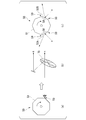
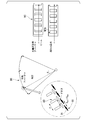






Classifications
-
- G—PHYSICS
- G03—PHOTOGRAPHY; CINEMATOGRAPHY; ANALOGOUS TECHNIQUES USING WAVES OTHER THAN OPTICAL WAVES; ELECTROGRAPHY; HOLOGRAPHY
- G03F—PHOTOMECHANICAL PRODUCTION OF TEXTURED OR PATTERNED SURFACES, e.g. FOR PRINTING, FOR PROCESSING OF SEMICONDUCTOR DEVICES; MATERIALS THEREFOR; ORIGINALS THEREFOR; APPARATUS SPECIALLY ADAPTED THEREFOR
- G03F7/00—Photomechanical, e.g. photolithographic, production of textured or patterned surfaces, e.g. printing surfaces; Materials therefor, e.g. comprising photoresists; Apparatus specially adapted therefor
- G03F7/70—Microphotolithographic exposure; Apparatus therefor
- G03F7/70483—Information management; Active and passive control; Testing; Wafer monitoring, e.g. pattern monitoring
- G03F7/7055—Exposure light control in all parts of the microlithographic apparatus, e.g. pulse length control or light interruption
-
- B—PERFORMING OPERATIONS; TRANSPORTING
- B23—MACHINE TOOLS; METAL-WORKING NOT OTHERWISE PROVIDED FOR
- B23K—SOLDERING OR UNSOLDERING; WELDING; CLADDING OR PLATING BY SOLDERING OR WELDING; CUTTING BY APPLYING HEAT LOCALLY, e.g. FLAME CUTTING; WORKING BY LASER BEAM
- B23K26/00—Working by laser beam, e.g. welding, cutting or boring
- B23K26/02—Positioning or observing the workpiece, e.g. with respect to the point of impact; Aligning, aiming or focusing the laser beam
- B23K26/06—Shaping the laser beam, e.g. by masks or multi-focusing
- B23K26/062—Shaping the laser beam, e.g. by masks or multi-focusing by direct control of the laser beam
- B23K26/0622—Shaping the laser beam, e.g. by masks or multi-focusing by direct control of the laser beam by shaping pulses
-
- B—PERFORMING OPERATIONS; TRANSPORTING
- B23—MACHINE TOOLS; METAL-WORKING NOT OTHERWISE PROVIDED FOR
- B23K—SOLDERING OR UNSOLDERING; WELDING; CLADDING OR PLATING BY SOLDERING OR WELDING; CUTTING BY APPLYING HEAT LOCALLY, e.g. FLAME CUTTING; WORKING BY LASER BEAM
- B23K26/00—Working by laser beam, e.g. welding, cutting or boring
- B23K26/02—Positioning or observing the workpiece, e.g. with respect to the point of impact; Aligning, aiming or focusing the laser beam
- B23K26/06—Shaping the laser beam, e.g. by masks or multi-focusing
- B23K26/0604—Shaping the laser beam, e.g. by masks or multi-focusing by a combination of beams
-
- B—PERFORMING OPERATIONS; TRANSPORTING
- B23—MACHINE TOOLS; METAL-WORKING NOT OTHERWISE PROVIDED FOR
- B23K—SOLDERING OR UNSOLDERING; WELDING; CLADDING OR PLATING BY SOLDERING OR WELDING; CUTTING BY APPLYING HEAT LOCALLY, e.g. FLAME CUTTING; WORKING BY LASER BEAM
- B23K26/00—Working by laser beam, e.g. welding, cutting or boring
- B23K26/02—Positioning or observing the workpiece, e.g. with respect to the point of impact; Aligning, aiming or focusing the laser beam
- B23K26/06—Shaping the laser beam, e.g. by masks or multi-focusing
- B23K26/064—Shaping the laser beam, e.g. by masks or multi-focusing by means of optical elements, e.g. lenses, mirrors or prisms
-
- B—PERFORMING OPERATIONS; TRANSPORTING
- B23—MACHINE TOOLS; METAL-WORKING NOT OTHERWISE PROVIDED FOR
- B23K—SOLDERING OR UNSOLDERING; WELDING; CLADDING OR PLATING BY SOLDERING OR WELDING; CUTTING BY APPLYING HEAT LOCALLY, e.g. FLAME CUTTING; WORKING BY LASER BEAM
- B23K26/00—Working by laser beam, e.g. welding, cutting or boring
- B23K26/02—Positioning or observing the workpiece, e.g. with respect to the point of impact; Aligning, aiming or focusing the laser beam
- B23K26/06—Shaping the laser beam, e.g. by masks or multi-focusing
- B23K26/067—Dividing the beam into multiple beams, e.g. multi-focusing
- B23K26/0676—Dividing the beam into multiple beams, e.g. multi-focusing into dependently operating sub-beams, e.g. an array of spots with fixed spatial relationship or for performing simultaneously identical operations
-
- B—PERFORMING OPERATIONS; TRANSPORTING
- B23—MACHINE TOOLS; METAL-WORKING NOT OTHERWISE PROVIDED FOR
- B23K—SOLDERING OR UNSOLDERING; WELDING; CLADDING OR PLATING BY SOLDERING OR WELDING; CUTTING BY APPLYING HEAT LOCALLY, e.g. FLAME CUTTING; WORKING BY LASER BEAM
- B23K26/00—Working by laser beam, e.g. welding, cutting or boring
- B23K26/08—Devices involving relative movement between laser beam and workpiece
- B23K26/082—Scanning systems, i.e. devices involving movement of the laser beam relative to the laser head
- B23K26/0821—Scanning systems, i.e. devices involving movement of the laser beam relative to the laser head using multifaceted mirrors, e.g. polygonal mirror
-
- B—PERFORMING OPERATIONS; TRANSPORTING
- B23—MACHINE TOOLS; METAL-WORKING NOT OTHERWISE PROVIDED FOR
- B23K—SOLDERING OR UNSOLDERING; WELDING; CLADDING OR PLATING BY SOLDERING OR WELDING; CUTTING BY APPLYING HEAT LOCALLY, e.g. FLAME CUTTING; WORKING BY LASER BEAM
- B23K26/00—Working by laser beam, e.g. welding, cutting or boring
- B23K26/36—Removing material
- B23K26/362—Laser etching
-
- B—PERFORMING OPERATIONS; TRANSPORTING
- B23—MACHINE TOOLS; METAL-WORKING NOT OTHERWISE PROVIDED FOR
- B23K—SOLDERING OR UNSOLDERING; WELDING; CLADDING OR PLATING BY SOLDERING OR WELDING; CUTTING BY APPLYING HEAT LOCALLY, e.g. FLAME CUTTING; WORKING BY LASER BEAM
- B23K26/00—Working by laser beam, e.g. welding, cutting or boring
- B23K26/36—Removing material
- B23K26/40—Removing material taking account of the properties of the material involved
- B23K26/402—Removing material taking account of the properties of the material involved involving non-metallic material, e.g. isolators
-
- G—PHYSICS
- G02—OPTICS
- G02F—OPTICAL DEVICES OR ARRANGEMENTS FOR THE CONTROL OF LIGHT BY MODIFICATION OF THE OPTICAL PROPERTIES OF THE MEDIA OF THE ELEMENTS INVOLVED THEREIN; NON-LINEAR OPTICS; FREQUENCY-CHANGING OF LIGHT; OPTICAL LOGIC ELEMENTS; OPTICAL ANALOGUE/DIGITAL CONVERTERS
- G02F1/00—Devices or arrangements for the control of the intensity, colour, phase, polarisation or direction of light arriving from an independent light source, e.g. switching, gating or modulating; Non-linear optics
- G02F1/01—Devices or arrangements for the control of the intensity, colour, phase, polarisation or direction of light arriving from an independent light source, e.g. switching, gating or modulating; Non-linear optics for the control of the intensity, phase, polarisation or colour
- G02F1/13—Devices or arrangements for the control of the intensity, colour, phase, polarisation or direction of light arriving from an independent light source, e.g. switching, gating or modulating; Non-linear optics for the control of the intensity, phase, polarisation or colour based on liquid crystals, e.g. single liquid crystal display cells
- G02F1/1303—Apparatus specially adapted to the manufacture of LCDs
-
- G—PHYSICS
- G03—PHOTOGRAPHY; CINEMATOGRAPHY; ANALOGOUS TECHNIQUES USING WAVES OTHER THAN OPTICAL WAVES; ELECTROGRAPHY; HOLOGRAPHY
- G03F—PHOTOMECHANICAL PRODUCTION OF TEXTURED OR PATTERNED SURFACES, e.g. FOR PRINTING, FOR PROCESSING OF SEMICONDUCTOR DEVICES; MATERIALS THEREFOR; ORIGINALS THEREFOR; APPARATUS SPECIALLY ADAPTED THEREFOR
- G03F7/00—Photomechanical, e.g. photolithographic, production of textured or patterned surfaces, e.g. printing surfaces; Materials therefor, e.g. comprising photoresists; Apparatus specially adapted therefor
- G03F7/70—Microphotolithographic exposure; Apparatus therefor
- G03F7/70008—Production of exposure light, i.e. light sources
- G03F7/70025—Production of exposure light, i.e. light sources by lasers
-
- G—PHYSICS
- G03—PHOTOGRAPHY; CINEMATOGRAPHY; ANALOGOUS TECHNIQUES USING WAVES OTHER THAN OPTICAL WAVES; ELECTROGRAPHY; HOLOGRAPHY
- G03F—PHOTOMECHANICAL PRODUCTION OF TEXTURED OR PATTERNED SURFACES, e.g. FOR PRINTING, FOR PROCESSING OF SEMICONDUCTOR DEVICES; MATERIALS THEREFOR; ORIGINALS THEREFOR; APPARATUS SPECIALLY ADAPTED THEREFOR
- G03F7/00—Photomechanical, e.g. photolithographic, production of textured or patterned surfaces, e.g. printing surfaces; Materials therefor, e.g. comprising photoresists; Apparatus specially adapted therefor
- G03F7/70—Microphotolithographic exposure; Apparatus therefor
- G03F7/70008—Production of exposure light, i.e. light sources
- G03F7/7005—Production of exposure light, i.e. light sources by multiple sources, e.g. light-emitting diodes [LED] or light source arrays
-
- G—PHYSICS
- G03—PHOTOGRAPHY; CINEMATOGRAPHY; ANALOGOUS TECHNIQUES USING WAVES OTHER THAN OPTICAL WAVES; ELECTROGRAPHY; HOLOGRAPHY
- G03F—PHOTOMECHANICAL PRODUCTION OF TEXTURED OR PATTERNED SURFACES, e.g. FOR PRINTING, FOR PROCESSING OF SEMICONDUCTOR DEVICES; MATERIALS THEREFOR; ORIGINALS THEREFOR; APPARATUS SPECIALLY ADAPTED THEREFOR
- G03F7/00—Photomechanical, e.g. photolithographic, production of textured or patterned surfaces, e.g. printing surfaces; Materials therefor, e.g. comprising photoresists; Apparatus specially adapted therefor
- G03F7/70—Microphotolithographic exposure; Apparatus therefor
- G03F7/70058—Mask illumination systems
- G03F7/70091—Illumination settings, i.e. intensity distribution in the pupil plane or angular distribution in the field plane; On-axis or off-axis settings, e.g. annular, dipole or quadrupole settings; Partial coherence control, i.e. sigma or numerical aperture [NA]
- G03F7/70116—Off-axis setting using a programmable means, e.g. liquid crystal display [LCD], digital micromirror device [DMD] or pupil facets
-
- G—PHYSICS
- G03—PHOTOGRAPHY; CINEMATOGRAPHY; ANALOGOUS TECHNIQUES USING WAVES OTHER THAN OPTICAL WAVES; ELECTROGRAPHY; HOLOGRAPHY
- G03F—PHOTOMECHANICAL PRODUCTION OF TEXTURED OR PATTERNED SURFACES, e.g. FOR PRINTING, FOR PROCESSING OF SEMICONDUCTOR DEVICES; MATERIALS THEREFOR; ORIGINALS THEREFOR; APPARATUS SPECIALLY ADAPTED THEREFOR
- G03F7/00—Photomechanical, e.g. photolithographic, production of textured or patterned surfaces, e.g. printing surfaces; Materials therefor, e.g. comprising photoresists; Apparatus specially adapted therefor
- G03F7/70—Microphotolithographic exposure; Apparatus therefor
- G03F7/70058—Mask illumination systems
- G03F7/70191—Optical correction elements, filters or phase plates for controlling intensity, wavelength, polarisation, phase or the like
-
- G—PHYSICS
- G03—PHOTOGRAPHY; CINEMATOGRAPHY; ANALOGOUS TECHNIQUES USING WAVES OTHER THAN OPTICAL WAVES; ELECTROGRAPHY; HOLOGRAPHY
- G03F—PHOTOMECHANICAL PRODUCTION OF TEXTURED OR PATTERNED SURFACES, e.g. FOR PRINTING, FOR PROCESSING OF SEMICONDUCTOR DEVICES; MATERIALS THEREFOR; ORIGINALS THEREFOR; APPARATUS SPECIALLY ADAPTED THEREFOR
- G03F7/00—Photomechanical, e.g. photolithographic, production of textured or patterned surfaces, e.g. printing surfaces; Materials therefor, e.g. comprising photoresists; Apparatus specially adapted therefor
- G03F7/70—Microphotolithographic exposure; Apparatus therefor
- G03F7/70058—Mask illumination systems
- G03F7/70208—Multiple illumination paths, e.g. radiation distribution devices, microlens illumination systems, multiplexers or demultiplexers for single or multiple projection systems
-
- G—PHYSICS
- G03—PHOTOGRAPHY; CINEMATOGRAPHY; ANALOGOUS TECHNIQUES USING WAVES OTHER THAN OPTICAL WAVES; ELECTROGRAPHY; HOLOGRAPHY
- G03F—PHOTOMECHANICAL PRODUCTION OF TEXTURED OR PATTERNED SURFACES, e.g. FOR PRINTING, FOR PROCESSING OF SEMICONDUCTOR DEVICES; MATERIALS THEREFOR; ORIGINALS THEREFOR; APPARATUS SPECIALLY ADAPTED THEREFOR
- G03F7/00—Photomechanical, e.g. photolithographic, production of textured or patterned surfaces, e.g. printing surfaces; Materials therefor, e.g. comprising photoresists; Apparatus specially adapted therefor
- G03F7/70—Microphotolithographic exposure; Apparatus therefor
- G03F7/70216—Mask projection systems
- G03F7/70275—Multiple projection paths, e.g. array of projection systems, microlens projection systems or tandem projection systems
-
- G—PHYSICS
- G03—PHOTOGRAPHY; CINEMATOGRAPHY; ANALOGOUS TECHNIQUES USING WAVES OTHER THAN OPTICAL WAVES; ELECTROGRAPHY; HOLOGRAPHY
- G03F—PHOTOMECHANICAL PRODUCTION OF TEXTURED OR PATTERNED SURFACES, e.g. FOR PRINTING, FOR PROCESSING OF SEMICONDUCTOR DEVICES; MATERIALS THEREFOR; ORIGINALS THEREFOR; APPARATUS SPECIALLY ADAPTED THEREFOR
- G03F7/00—Photomechanical, e.g. photolithographic, production of textured or patterned surfaces, e.g. printing surfaces; Materials therefor, e.g. comprising photoresists; Apparatus specially adapted therefor
- G03F7/70—Microphotolithographic exposure; Apparatus therefor
- G03F7/70216—Mask projection systems
- G03F7/70283—Mask effects on the imaging process
- G03F7/70291—Addressable masks, e.g. spatial light modulators [SLMs], digital micro-mirror devices [DMDs] or liquid crystal display [LCD] patterning devices
-
- H—ELECTRICITY
- H10—SEMICONDUCTOR DEVICES; ELECTRIC SOLID-STATE DEVICES NOT OTHERWISE PROVIDED FOR
- H10K—ORGANIC ELECTRIC SOLID-STATE DEVICES
- H10K71/00—Manufacture or treatment specially adapted for the organic devices covered by this subclass
- H10K71/20—Changing the shape of the active layer in the devices, e.g. patterning
- H10K71/231—Changing the shape of the active layer in the devices, e.g. patterning by etching of existing layers
- H10K71/233—Changing the shape of the active layer in the devices, e.g. patterning by etching of existing layers by photolithographic etching
-
- B—PERFORMING OPERATIONS; TRANSPORTING
- B23—MACHINE TOOLS; METAL-WORKING NOT OTHERWISE PROVIDED FOR
- B23K—SOLDERING OR UNSOLDERING; WELDING; CLADDING OR PLATING BY SOLDERING OR WELDING; CUTTING BY APPLYING HEAT LOCALLY, e.g. FLAME CUTTING; WORKING BY LASER BEAM
- B23K2101/00—Articles made by soldering, welding or cutting
- B23K2101/36—Electric or electronic devices
- B23K2101/40—Semiconductor devices
-
- B—PERFORMING OPERATIONS; TRANSPORTING
- B23—MACHINE TOOLS; METAL-WORKING NOT OTHERWISE PROVIDED FOR
- B23K—SOLDERING OR UNSOLDERING; WELDING; CLADDING OR PLATING BY SOLDERING OR WELDING; CUTTING BY APPLYING HEAT LOCALLY, e.g. FLAME CUTTING; WORKING BY LASER BEAM
- B23K2103/00—Materials to be soldered, welded or cut
- B23K2103/50—Inorganic materials other than metals or composite materials
- B23K2103/54—Glass
Definitions
- the present invention relates to an optical device including a laser light source, an exposure device, a method for manufacturing a flat panel display, and a method for manufacturing a device.
- Laser beams are used in various fields.
- the optical device is arranged between a plurality of laser light sources, an output module having an optical modulator, and the plurality of laser light sources and the output module, and is emitted from the plurality of laser light sources. It is provided with a time divider that divides the laser beam in time.
- the optical device is disposed between a plurality of laser light sources, a plurality of output modules each having a light modulator, and the plurality of laser light sources and the plurality of output modules.
- a time divider that temporally divides the laser light emitted from the plurality of laser light sources is provided.
- the optical device is arranged between a plurality of output modules, each having a light modulator, and the plurality of laser light sources and the plurality of output modules, from the plurality of laser light sources.
- the optical device is arranged between the laser light source, the output module, and the laser light source and the output module, and temporally divides the laser light emitted from the laser light source. It is equipped with a time divider. The time divider divides the laser beam using a plurality of reflecting surfaces.
- the optical device is arranged between the laser light source, the plurality of output modules, and the laser light source and the plurality of output modules, and the laser light emitted from the laser light source is timed. It is provided with a time divider for dividing the laser. The time divider divides the laser beam using a plurality of reflecting surfaces.
- the optical device includes a laser light source, an output module having an optical modulator, and an acoustic optical element arranged between the light source and the output module.
- the optical device comprises a laser light source, a plurality of output modules each having a light modulator, and an acoustic optical element arranged between the laser light source and the output module. Be prepared.
- the optical device is arranged between a laser light source that emits pulsed light, an output module having an optical modulator, and the laser light source and the output module, and the pulsed light is timed. It is provided with a time divider for subjecting the pulse light and a controller for controlling the division of the pulsed light by the time divider based on the frequency of the pulsed light.
- the optical device is disposed between a laser light source that emits pulsed light, a plurality of output modules each having a light modulator, and the laser light source and the plurality of output modules.
- a time divider for temporally dividing the pulsed light and a controller for controlling the division of the pulsed light by the time divider based on the frequency of the pulsed light are provided.
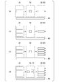
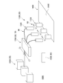
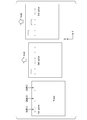
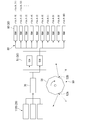
- FIG. 1 is a schematic view showing various morphological examples of a laser beam system (optical device) including a laser light source.
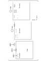
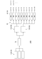
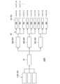
- FIG. 2 is a schematic view showing another various embodiment of a laser beam system (optical device) including a laser light source.
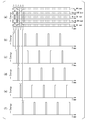
- FIG. 3 is a diagram showing an example of synthesis control of a pulsed laser beam.
- FIG. 4 is a diagram showing an example of synthesis control of the CW laser beam.
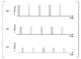
- FIG. 5 is a diagram showing an example of an output beam.
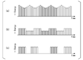
- FIG. 6 is a diagram showing another example of the output beam.
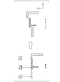
- FIG. 7 is a diagram showing an example in which a polygon mirror device is applied as a time divider (rotating device).
- FIG. 1 is a schematic view showing various morphological examples of a laser beam system (optical device) including a laser light source.
- FIG. 2 is a schematic view showing another various embodiment of a laser beam system (optical device) including a laser light source.
- FIG. 3 is a diagram showing
- FIG. 8 is a diagram showing an example in which a polygon mirror device is applied as a time divider (rotating device).
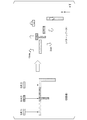
- FIG. 9 is a diagram showing an example in which an optical switch device is applied as a time divider (rotating device).
- FIG. 10 is a diagram showing an example in which an optical switch device is applied as a time divider (rotating device).
- FIG. 11 is a diagram showing an example in which an optical switch device is applied as a sub-divider (dynamic time-divider) and a polygon mirror device is applied as a time-divider (dynamic time-divider).
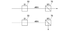
- FIG. 12 is a diagram showing an example in which an electro-optical modulator is applied as a time divider and a polarizing beam splitter is applied as a sub-splitter (static splitter).
- FIG. 9 is a diagram showing an example in which an optical switch device is applied as a time divider (rotating device).
- FIG. 10 is a diagram showing an example in which an optical switch device is applied as a
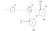
- FIG. 13 is a diagram showing an example in which an electro-optical modulator is applied as a sub-divider (dynamic time-divider) and a polarizing beam splitter is applied as a sub-splitter (static splitter).
- FIG. 14 is a diagram showing an example of including an aperture device arranged on an optical path.
- FIG. 15 is a diagram schematically showing the overall configuration of the exposure apparatus.
- FIG. 16 is a diagram showing a configuration example of the exposure apparatus.
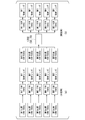
- FIG. 17 is a diagram for explaining the relationship between the repetition frequency of the laser beam and the operating frequency of the SLM.
- FIG. 18 is a diagram for explaining a combination of a light source and an output module.
- FIG. 19 is a diagram showing an example of the configuration of an exposure apparatus not provided with SLM.
- FIG. 20 is a diagram showing an example of the configuration of an exposure apparatus including SLM.
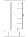
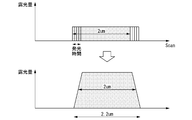
- FIG. 21 is a diagram for explaining the relationship between the pattern line width and the light emission time.
- FIG. 22 is a diagram for explaining the energy loss of the beam.
- FIG. 23 is a diagram for explaining time division of the beam.
- FIG. 24 is a diagram for explaining the deviation of the projection position among the plurality of SLMs based on the irradiation timing.
- FIG. 25 is a diagram for explaining mechanical and / or optical shift adjustment.
- FIG. 26 is a diagram for explaining shift adjustment corresponding to the scanning operation.
- FIG. 27 is a diagram for explaining shift adjustment corresponding to another scanning operation.
- FIG. 28 is a diagram showing a configuration example of an exposure apparatus for shift adjustment.
- FIG. 21 is a diagram for explaining the relationship between the pattern line width and the light emission time.
- FIG. 22 is a diagram for explaining the energy loss of the beam.
- FIG. 23 is a diagram for explaining time division of
- FIG. 29 is a diagram showing a configuration example of the exposure apparatus.
- FIG. 30 is a diagram showing a configuration example of the exposure apparatus.
- FIG. 31 is a diagram showing a configuration example of the exposure apparatus.
- FIG. 32 is a diagram showing a configuration example of the exposure apparatus.
- FIG. 33 is a diagram showing a configuration example of the exposure apparatus.
- FIG. 34 is a diagram showing a configuration example of the exposure apparatus.
- FIG. 35 is a diagram showing an example of pattern exposure.
- FIG. 36 is a diagram showing a configuration example of an exposure apparatus for synchronous control.
- FIG. 37 is a diagram for explaining an example of rotation control of the polygon mirror.
- FIG. 38 is a diagram for explaining an example of synchronization control of the polygon mirror.
- FIG. 39 is a diagram for explaining operation timings of a plurality of devices.
- FIG. 40 is a diagram for explaining an example of synchronous control of the rotating plate.
- FIG. 41 is a diagram for explaining an example of synchronous control of the rotary plate that has been subjected to additional processing.
- 1 and 2 are schematic views showing various morphological examples of a laser beam system (optical device) including a laser light source. 1 (a), 1 (b), 1 (c), 1 (d), 2 (a), 2 (b), 2 (c), and 2 (d).
- the laser beam system comprises a laser light source 20.
- the laser beam system (optical device) is arranged optically between the laser light source 20, the output module 30, the controller 40, and the laser light source 20 and the output module 30.
- the time divider 50 and the like are provided.
- laser light sources 20 can be applied.
- gas laser helium neon laser, argon laser, carbon dioxide gas laser, excima laser, nitrogen laser, etc.
- semiconductor laser solid-state laser (YAG laser, Nd (neodim) laser, ruby laser, fiber laser, titanium laser, etc.) Etc.
- metal lasers copper vapor deposition lasers, helium cadmium lasers, gold vapor deposition lasers, etc.
- liquid lasers etc.
- the technique of the present disclosure can be applied to various oscillation forms such as pulse oscillation and continuous wave (CW) oscillation.
- the output module 30 is set according to the application of the laser beam.
- the laser beam includes a laser processing device, a laser melting device, a laser welding device, a laser marking device, a laser length measuring device, a semiconductor exposure device, a flat panel display exposure device, a circuit board exposure device, a laser illumination device, and a laser display device. It is used in optical devices such as laser detection devices, laser propulsion devices, laser inspection devices, laser microscopes, and laser medical devices. The techniques of the present disclosure are applicable to devices in various fields, including these devices.
- the output module 30 includes a Spatial Light Modulator (SLM) 60.
- SLM Spatial Light Modulator
- the SLM 60 includes a liquid crystal element, a digital mirror device (digital micromirror device, DMD), a magneto-optical spatial light modulator (Magneto Optic Spatial Light Modulator, MOSLM), and the like.
- the time divider (time divider, dynamic time divider, optical time divider, optical switch, optical shutter, dynamic switch, dynamic shutter, dynamic separator, optical path switcher) 50 is controlled by the controller 40.
- the laser beam is configured to be time-divided.
- examples of the time divider 50 include a polygon mirror device, a galvano mirror device, an electro-optical modulator (EOM), an acousto-optic modulator (AOM), a vibration device, and other optical switch devices (liquid crystal switch, etc.). .. Time-division beams are selectively available. In addition, the time-division multiple beams can be combined, mixed, and / or converged.
- the selectively extracted beam from the time divider 50 enters the output module 30.
- the time-division beam is guided through a plurality of optical paths at predetermined spans on the time axis.
- a plurality of time-divided beams are supplied to a plurality of paths, respectively.
- the time divider 50 is controlled to be driven synchronously with the SLM 60 of the output module 30.
- a time-division beam corresponding to the drive timing of the SLM 60 is supplied to the SLM 60.
- the operating frequency of the SLM 60 for example, the image update frequency
- the beam corresponding to the operation timing of the SLM 60 is selectively used. The remaining beams of the time-division beams can be used for other purposes.
- the time divider 50 may be controlled to drive asynchronously with the SLM 60 of the output module 30.
- the laser beam system comprises a plurality of laser light sources 20.
- the number of laser light sources 20 can be set arbitrarily.
- the number of laser light sources 20 is 2, 3, 4, 5, 6, 7, 8, 9, 10, 11, 12, 13, 14, 15, 16, 17, 18, 19, 20, or more. Can be done.
- beams from a plurality of laser light sources 20 are combined, mixed, and / or converged into a time divider 50 via a predetermined device.
- the beams from the plurality of laser light sources 20 can have relatively high energy values even after being divided by the time divider 50.
- the beams from the plurality of laser light sources 20 enter the time divider 50 independently.
- the beams from the plurality of pulsed laser light sources 20 are set so that the pulse width and the peak value (pulse waveform, waveform profile) are substantially the same as each other. In another example, the beams from the plurality of pulsed laser light sources 20 are set so that at least one of the pulse width and the peak value (pulse waveform, waveform profile) is different from each other.
- the energy loss of the laser beam is reduced, the energy efficiency is improved, and the output intensity of the laser beam is appropriately controlled. And / or speckle is suppressed.
- the beam from the time divider 50 is supplied to the SLM 60 at the appropriate time.
- the energy loss in the SLM60 is reduced, and the high energy beam (high power beam) is output from the output module 30.
- the laser beam system comprises a plurality of output modules 30.
- the first time-division beam is supplied to the first output module 30, and the second time-division beam is supplied to the second output module 30.
- the number of output modules 30 can be set arbitrarily.
- the number of output modules 30 is 2, 3, 4, 5, 6, 7, 8, 9, 10, 11, 12, 13, 14, 15, 16, 17, 18, 19, 20, 25, 30. , 35, 40, 45, 50, or more.
- each of the plurality of output modules 30 has an SLM60.
- the plurality of SLM60s are driven synchronously or asynchronously with each other.
- the first, second, third, and fourth SLM60s are driven at the same timing, corresponding to a time division beam.
- the first and second SLM60s are driven at the same timing corresponding to the first time-division beam
- the third and fourth SLM60s are driven at different timings corresponding to the second time-division beam. Will be done.
- the first SLM60 is driven at a timing corresponding to the first time-division beam
- the second SLM60 is driven at another timing corresponding to the second time-division beam
- the third SLM60 is driven. Is driven at yet another timing corresponding to the third time division beam
- the fourth SLM60 is driven at yet another timing corresponding to the fourth time division beam.
- the time divider 50 and the plurality of SLMs 60 are combined, for example, the energy loss of the laser beam is reduced, the energy efficiency is improved, the output intensity of the laser beam is appropriately controlled, and the beam output timing is set. Properly controlled and / or the output beam waveform is properly controlled.
- the beam from the laser light source 20 is guided to the plurality of SLM 60s so as to correspond to the drive timings of the plurality of SLM 60s. Reducing the beam shading period (beam non-use period) is advantageous for improving energy efficiency, reducing leakage light, and / or avoiding thermal effects.
- the laser beam system is located between the laser light source 20 and the time divider 50 optically, or between the time divider 50 and the output module 30.
- a time divider, a dynamic time divider, an optical time divider, an optical switch, an optical shutter, a dynamic switch, a dynamic shutter, a dynamic separator, an optical path switcher) 70 are further provided.
- the sub-divider 70 includes a dynamic or static divider and is configured to split the laser beam by polarization, frequency separation, or time.
- the dynamic divider means a configuration that separates or divides the laser beam with the drive of the divider
- the static divider means a configuration that separates or divides the laser beam without driving the divider. means.
- the dynamic divider the same one as the time divider described above can be applied.
- a static splitter a polarizing beam splitter, a half mirror, a dichroic mirror, a frequency separator and the like are exemplified.
- the time divider 50 and the static divider 70 are sequentially arranged on the optical axis along the traveling direction of the beam.
- the static divider 70 and the time divider 50 are arranged in order on the optical axis along the traveling direction of the beam.
- a time divider (front position, front stage time divider) 70 and a time divider (rear position, rear stage time divider) 50 are arranged in order on the optical axis along the traveling direction of the beam.
- a plurality of time dividers 50, 70 are combined.
- one time divider 50 and a plurality of static dividers 70 are combined.
- a plurality of time dividers 50 and one static divider 70 are combined.
- the plurality of time dividers 50 and the plurality of static dividers 70 are combined.
- the number of the time divider 50 and the sub-divider 70 can be set arbitrarily.
- the total number of time dividers 50 and sub-dividers 70 is 2, 3, 4, 5, 6, 7, 8, 9, 10, 11, 12, 13, 14, 15, 16, 17, 18, It can be 19, 20, or more.
- the time divider 50 and the static divider 70 are combined, for example, the energy loss of the laser beam is reduced, the energy efficiency is improved, the output intensity of the laser beam is appropriately controlled, and the beam output.
- the timing is properly controlled and / or the output beam waveform is properly controlled.
- the number of divisions of the beam is expanded and / or the beam is divided into a plurality of parts according to the wavelength band.
- the time divider (front position) 70 and the time divider (rear position) 50 are combined, for example, the energy loss of the laser beam is reduced, the energy efficiency is improved, and the output intensity of the laser beam is appropriate.
- the beam output timing is appropriately controlled, and / or the output beam waveform is appropriately controlled. In one example, the number of beam divisions is increased and / or the use of unstable and / or unsuitable zones in the time divider is avoided while suppressing energy loss.
- the time-sharing beam from the front-position time-divider 70 enters the rear-position time-divider 50 in the first span on the time axis, and the stable zone and / or preferred zone of the rear-position time-divider 50 is preferentially and / or preferred. / Or preferably used (specifically and / or preferentially).
- the time-division beam from the front-position time-divider 70 does not substantially enter the rear-position time-divider 50, and the unstable zone and / or non-stability of the rear-position time-divider 50. The use of suitable zones is avoided.
- each of the plurality of time dividers 50 at the rear position has a stable zone (suitable zone) and an unstable zone (non-suitable zone).
- a plurality of time dividers 50 at the rear positions are driven so that the stable states at the time of driving are at different timings.
- the time-dividing beam from the time-dividing device 70 at the front position is distributed so as to match the stable state of each time-dividing device 50 at the rear position.
- the output module 30 has an optical fiber.
- the optical fiber is configured to receive a plurality of time-division beams from the time-divider 50 or the sub-divider 70.
- one optical fiber is provided for one output module 30.
- a plurality of optical fibers are provided for one output module 30.
- a plurality of time-division beams from a plurality of optical fibers are incident on one output module 30.
- the laser beam system has a plurality of output modules 30.
- Each of the plurality of output modules 30 includes a fiber.
- the time-division beam at the first timing is supplied to the first optical fiber
- the time-division beam at the second timing is supplied to the second optical fiber.
- one optical fiber is provided for each of the plurality of output modules 30.
- a plurality of optical fibers are provided for each of the plurality of output modules 30.
- a plurality of time-division beams from the plurality of optical fibers are incident on each of the plurality of output modules 30.
- FIG. 3 is a diagram showing an example of synthesis control of a pulsed laser beam.
- FIG. 4 is a diagram showing an example of synthesis control of the CW laser beam.
- 5 and 6 are diagrams showing an example of an output beam. In each example, a power-controlled laser beam is output from the laser beam system.
- a plurality of laser beams emitted from a plurality of light sources 20 are combined. Synthesis can be performed by optics including lenses, beam splitters, harbbing or mirrors and the like.
- the combined laser beam is incident on the time divider 50, and the synthesized beam (combined beam of the first pulse) corresponding to the first repetition timing is guided to the first optical fiber 80 via the time divider 50 (the synthesized beam of the first pulse). 3 (b) and 4 (b).
- a composite beam corresponding to the second repetition timing is guided to the second optical fiber 80 via the time divider 50 (FIGS. 3 (c) and 4 (c)).
- a composite beam corresponding to the third repetition timing is guided to the third optical fiber 80 via the time divider 50 (FIGS. 3 (d) and 4 (d)).
- a composite beam corresponding to the fourth repetition timing is guided to the fourth optical fiber 80 via the time divider 50 (FIGS. 3 (e) and 4 (e)).
- a composite beam corresponding to the fifth repetition timing is guided to the fifth optical fiber 80 via the time divider 50 (FIGS. 3 (f) and 4 (f)).
- the first, second, third, fourth, and fifth repetition timings are time-shifted in order.
- a high-energy (high-power) synthetic beam is guided to each optical fiber 80.
- the composite beam is guided to the optical fiber 80 in accordance with the operation timing of the SLM 60 having a relatively low speed.
- the output powers can be controlled to be different from each other among the plurality of output modules 30.
- a relatively high energy (high power) beam is output from the first output module 30 (FIG. 5A).
- a beam of intermediate energy (intermediate power) is output from the second output module 30 (FIG. 5 (b)).
- a relatively low energy (low power) beam is output from the third output module 30 (FIG. 5 (c)).
- the application of a combination of time division and synthesis appropriately controls the output beam waveforms from one or more output modules 30 (FIGS. 6 (a) and 6 (b)). And / or the beam output timing from one or more output modules 30 is appropriately controlled (FIG. 6 (c)).
- a rotating device (rotating switch) is applied as the time divider 50.
- the rotation device 50 is rotationally controlled by the controller 40 and is configured to timely divide the laser beam.
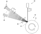
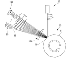
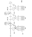
- a polygon mirror device is applied as the rotating device 50 (Fig. 7).
- the beam from the laser light source 20 is reflected by each of the plurality of reflecting surfaces 52 of the polygon mirror 51 in the polygon mirror device 50.
- Each of the plurality of output modules 30 has an optical fiber 80 having an inlet portion.
- the beam is time-divided according to the rotation angle of the polygon mirror 51.
- the beam reflected by the polygon mirror 51 is directed toward the inlet (incident surface) of any one of the plurality of optical fibers 80 according to the rotation angle of the polygon mirror 51.
- the rotation of the polygon mirror 51 changes the angle of the reflecting surface of the polygon mirror 51 with respect to the beam, and the destination of the beam reflected by the reflecting surface changes with time. Therefore, the beam of the first pulse from the laser light source 20 is incident on the first optical fiber, and the beam of the second pulse is incident on the second optical fiber whose position is different from that of the first optical fiber.
- a large number of optical fibers 80 can be arranged for one polygon mirror 51.
- the time-division beam from the polygon mirror 51 is distributed to any of the plurality of optical fibers 80. In other words, the polygon mirror 51 switches the optical fiber into which the beam is incident. In other words, the polygon mirror 51 switches the position of the optical path of the beam.
- At least one lens 85, 86 is arranged between the polygon mirror 51 and the optical fiber 80, if necessary (FIG. 8).
- the inlet portion (incident surface) of the optical fiber 80 and the reflection surface of the polygon mirror 51 are conjugate, the deviation (positional deviation) of the incident position of the beam with respect to the optical fiber 80 based on the rotation of the polygon mirror 51 is suppressed. Will be done.
- a slight change in the incident angle of the beam with respect to the optical fiber 80 based on the rotation of the polygon mirror 51 is advantageous for suppressing the speckle.
- a CW beam can also be applied to this embodiment.
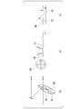
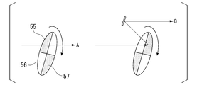
- a disk-shaped optical switch device is applied as the rotating device 50 (Fig. 9).
- the beam is time-divided according to the rotation angle of the rotating plate 55.
- the beam from the laser light source 20 is reflected or transmitted by the optical surfaces 56 and 57 of the rotating plate 55 in the optical switch device 50 according to the rotation angle of the rotating plate 55 (FIG. 9A).
- the rotating plate 55 has a transmission surface 56 and a reflection surface 57 arranged in the circumferential direction.
- the beam transmitted through the rotating plate 55 heads toward the first path “A”, and the beam reflected by the rotating plate 55 heads toward the second path “B” (FIG. 10).
- the beam from the laser light source 20 is reflected in different directions on the optical surfaces 56 and 57 of the rotating plate 55 in the optical switch device 50 according to the rotation angle of the rotating plate 55 (FIG. 9B).
- the rotating plate 55 has a first reflecting surface 56 and a second reflecting surface 57 having different orientations.
- the beam reflected by the first reflecting surface 56 of the rotating plate 55 heads toward the first path "A"
- the beam reflected by the second reflecting surface 57 of the rotating plate 55 heads toward the second path "B”.
- the beam from the laser light source 20 is reflected at different height positions of the rotating plate 55 according to the rotation angle of the rotating plate 55 (FIG. 9 (c)).
- the rotating plate 55 has a first reflecting surface 56 and a second reflecting surface 57 having different height positions in the rotation axis direction.
- the beam reflected by the first reflecting surface 56 of the rotating plate 55 heads toward the first path "A"
- the beam transmitted through the first reflecting surface of the rotating plate 55 and reflected by the second reflecting surface 57 is the second path. Head to "B”.
- the number of beam divisions in the rotary optical switch device 50 is not limited to 2.
- the number of divisions can be 3, 4, 5, 6, 7, 8, 9, 10, or more.
- the rotating plate 55 can have three or more reflective surfaces that are oriented differently from each other.
- the disk-type optical switch device described above is applied as a sub-divider (dynamic time-divider) 70, and the polygon mirror device is applied as a time-divider (dynamic time-divider) 50 ( FIG. 11).
- the use of a corner of the polygon mirror 51 as an unstable zone and / or an unsuitable zone 59 can be avoided.
- the beam from the optical switch device 70 is directed to the first position in the reflection surface 52 of the polygon mirror device 50 via the path "A", and the polygon mirror 51 (reflection surface 52A). It is reflected preferentially and / or preferentially in the stable zone 58 and time-divided.
- the beam from the optical switch device 70 is directed to the reflection surface 52B different from the reflection surface 52A of the polygon mirror device 50 via the path "B", and the polygon mirror 51 (reflection surface 52B) is stable.
- Zone 58 is preferentially and / or preferably reflected and timed. Beams are alternately supplied to the reflecting surface 52A and the reflecting surface 52B of the polygon mirror 51.
- the beam does not enter the reflection surface 52B, and the unstable zone (corner portion) 59 of the polygon mirror 51 (reflection surface 52A), that is, the portion where the reflection surface and the reflection surface forming the polygon mirror 51 intersect (the reflection surface). The use of (boundary part) is avoided.
- the beam does not enter the reflection surface 52A, and the use of the unstable zone (corner portion) 59 of the polygon mirror 51 (reflection surface 52B) is avoided.
- the use of the unstable zone in the polygon mirror 51 (time-dividing device 50) is avoided while the beam is substantially continuously used. Details of avoiding the use of unstable zones in the polygon mirror 51 (time divider 50) will be described later.
- the reflecting surface 52A and the reflecting surface 52B are changed with time by the rotation of the polygon mirror 51. That is, the reflection surface 52A is a surface on which the beam is incident on the polygon mirror device 50 via the path “A”. Further, the reflection surface 52B is a surface on which the beam is incident on the polygon mirror device 50 via the path “B”.
- an electro-optical modulator (EOM, EO) is applied as the time divider 50 and a polarizing beam splitter (PBS) is applied as the sub-splitter (static splitter) 70 (FIG. 12).
- EOM50 and PBS70 are arranged in order on the optical axis along the traveling direction of the beam.
- the beam from the EOM 50 is branched into a plurality of beams by the PBS 70 according to the wavelength band.
- a p-polarized beam of time-division beams from EOM50 passes through PBS70.
- the s-polarized beam of the time-division beam from EOM50 is reflected by PBS70.
- an electro-optic modulator (EOM, EO) is applied as a sub-divider (dynamic time-division) 70 and a polarizing beam splitter (PBS) is applied as a sub-splitter (static splitter) 70.
- a plurality of polygon mirror devices are applied as the time divider 50 (FIG. 13).
- the polygon mirrors 51A and 51B of the plurality of polygon mirror devices are arranged so as to be in a parallel positional relationship with respect to the optical path.
- the EOM 70, the PBS 70, and the polygon mirror 50 are arranged in order on the optical axis along the traveling direction of the beam.
- the beam from the EOM 70 is branched by the PBS 70 according to the wavelength band.
- the p-polarized beam transmitted through the PBS 70 is time-divisioned by the first polygon mirror 51A, and the s-polarized beam reflected by the PBS 70 is time-divisioned by the second polygon mirror 51B.
- the laser beam system further comprises an aperture device 90 that is optically located between the time divider 50 (or subdivider 70) and the optical fiber 80 (or output module 30) (FIG. 14).
- the aperture device 90 has an aperture 91, and the area of the opening through which the beam passes is controlled by the controller 40.
- the aperture 91 has a plurality of openings. In this embodiment, for example, among the beams from the time divider 50, the beam that has passed through the first aperture of the aperture 91 enters the first fiber as the first time division beam, and the beam that has passed through the second aperture is the second time. Enter the second fiber as a split beam. Further, by controlling the aperture area of the aperture 91, the amount of light of each time-division beam is adjusted. This form is preferably applied to a beam such as a CW laser beam having a relatively long emission time.
- the laser beam system is applied to a photolithography system for manufacturing devices (electronic devices or microdevices) such as semiconductor elements, liquid crystal display elements, and organic EL elements.
- a batch exposure type exposure device such as a stepper or a scanning exposure type exposure device such as a scanning stepper is used.
- a predetermined pattern is formed in each shot region of a substrate such as a wafer or a glass plate via a projection optical system.
- a pattern formed on a mask (or reticle) held on a mask stage is transferred to a substrate by irradiation of exposure light via a projection optical system.
- a spatial light modulator is used instead of the mask to generate a variable pattern on the object surface of the projection optical system (maskless exposure apparatus).
- the laser beam system is applied to an exposure apparatus as a photographic system for manufacturing a flat panel display (liquid crystal display device, organic EL display device, etc.).
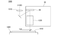
- the exposure device 1000 includes a light source module 1100 including a laser light source 20, a distribution module (synthesis / distribution module) 1200 including a time divider 50 and a sub-divider 70, and an output module (optical fiber 80 and illumination optical system (illumination system)).
- a lighting system 1300 including 1310, an SLM60, a projection optical system (projection lens) 1330) 30, a substrate stage 1400 on which a substrate (workpiece) 1410 is mounted, and a control system 1500 including a controller 40 and a data transmission unit.
- the light source module 1100 emits a laser beam of light energy.
- the beam from the light source module 1100 enters the illumination system 1310 via the distribution module 1200.
- the beam from the illumination system 1310 illuminates the SLM60.
- the controller generates pattern data based on the exposure pattern to be formed on the 40 substrate 1410.
- the controller 40 transmits pattern data to the SLM 60 and controls the SLM 60.
- the SLM 60 is controlled by the controller 40 and guides a beam from the illumination system to the substrate 1410 based on pattern data (simply expressed as image data or image).
- the projection lens 1330 projects the beam from the SLM 60 onto the substrate 1410 and forms an image on a predetermined region on the substrate 1410.
- the controller 40 divides the generated pattern data for each SLM60 and transmits the divided pattern data to each SLM60.
- a laser beam is emitted while the substrate stage 1400 on which the substrate is placed is moving, and the laser beam is guided to the SLM via the illumination optical system 1310.
- the image formed on the SLM is preferably exposed with a single emission of the laser beam.
- the same pattern data is projected on the substrate for each emission. Since the substrate 1410 is also moved between the emission of the laser beam and the emission by the substrate stage 1400, when the same pattern data is projected on the substrate, the substrate 1410 is exposed as if an image is flowing. If the scanning speed is increased to improve the throughput, the moving distance between the laser beam emission and the emission becomes longer, and the image flows more.
- the operating frequency of the SLM (for example, the image update frequency) is lower than the emission repetition frequency (oscillation frequency) of the laser beam, and is, for example, several kHz to several tens of kHz.
- the laser beam is 50 kHz (10 W) and the SLM is 10 kHz.
- a low-frequency oscillation frequency and a high-energy light source that does not cause exposure defects are desired in order to prevent the image from flowing, but the wavelength condition is also satisfied.
- the choice of laser light source is extremely limited at present.
- the above numerical values are examples, and the present invention is not limited thereto.
- a low frequency and high energy beam output is realized by combining a plurality of beams and time division.
- the distribution module 1200 synthesizes and time divides the beams from the five light sources 20.
- the beams emitted from the five light sources at a frequency of 50 kHz are combined into a high-energy beam.
- the combined beam (50 kHz, high energy) is time-division-guided to five SLM60s (and five projection lenses 1330) by the distribution module 1200, respectively. Therefore, a high-energy beam reaches each of the first to fifth SLMs at a frequency of 10 kHz.
- a light source of 50 W in total is used in 5 modules.
- the laser beam is 50 kHz (10 W) and the SLM is 10 kHz
- the light is distributed (distributed and switched) to the five SLMs by the distribution module 1200.
- the oscillation frequency of the laser beam is preferably an integral multiple of the image update frequency of the SLM.
- the distribution module 1200 distributes the laser beam to the number of SLMs that is an integral multiple of the above.
- the above numerical values are examples, and the present invention is not limited thereto.
- the intensity (eg, pulse energy, average power) E2 of the laser beam irradiated to one SLM is equivalent to the intensity (eg, pulse energy, average power) E1 of the laser beam emitted from one laser light source.
- E2 / E1 is about 1, 2, 3, 4, 5, 6, 7, 8, 9, 10, 11, 12, 13, 14, 15, 16, 17, 18, 19, 20, 25, It can be 30, 35, 40, 45, 50, 100 or more.
- the frequency (irradiation frequency) F2 of the beam irradiated to one SLM or the image update frequency F3 of the SLM is lower than the emission repetition frequency (oscillation frequency, light source frequency) F1 of the laser light source.
- F2 / F1 (or F3 / F1) is about 1/2, 1/3, 1/4, 1/5, 1/6, 1/7, 1/8, 1/9, 1/10, 1/11, 1/12, 1/13, 1/14, 1/15, 1/16, 1/17, 1/18, 1/19, 1/20, 1/25, 1/30, 1 / It can be 35, 1/40, 1/45, 1/50, 1/100 or less.
- the combination of multiple beam synthesis and time division is also applicable to systems without SLM (eg, exposure equipment), as shown in FIG.
- SLM eg, exposure equipment
- FIG. 19 exposure apparatus 1000
- a plurality of time-divided beams (a plurality of distributed beams) are generated for each predetermined span on the time axis.
- a relatively low frequency and high energy beam is supplied to each of the plurality of modules 30.
- the number of output modules 30 can be arbitrarily set.
- the distribution module 1200 synthesizes and time divides the beams from the four light sources 20. The time-division beam is supplied to each of the four SLM60s (module 30).
- the line width of the pattern is 2 ⁇ m and the scanning speed is 400 mm / s.
- the required emission time is within 0.5 ⁇ s.
- the operating frequency (image update frequency) of the SLM is 10 kHz.
- 10 kHz corresponds to 100 ⁇ s.
- the required light emission time is 0.5 ⁇ s
- the SLM is irradiated with a beam after 0.5 ⁇ s
- the same projected image is formed on the substrate 1410 to which the same projected image moves because the image on the SLM is not updated.
- the image flows as if it were flowing.
- the SLM In order to prevent the image from flowing, during the time from 0.5 ⁇ s to the next update of the image on the SLM, the SLM is not irradiated with the beam, for example, in the optical path from the CW light source to the SLM. Block the beam.
- the time from 0.5 ⁇ s or later until the next image on the SLM is updated is substantially a rest time.
- the substrate 1410 is exposed only with 1/200 of the energy from the light source.
- the operating frequency (image update frequency) of the SLM is 10 kHz.
- the frequency of the light source is 400 kHz
- the operating frequency of the SLM / the light source frequency 1/40, and only 1/40 of the energy from the light source is used. That is, only one of the 40 pulses oscillated from the pulse light source irradiates the SLM, in other words, 39 pulses do not irradiate the SLM, and the 39 pulses do not contribute to the exposure of the substrate 1410. Therefore, in the comparative examples of FIGS. 22 (a) and 22 (b), the exposure energy may be insufficient and exposure failure (photosensitivity failure) may occur.
- the above numerical values are examples, and the present invention is not limited thereto.
- the time-divided beam from the distribution module 1200 has a non-scan direction (non-scan direction, Y direction) that intersects the scan direction (scan direction, X direction) in which the substrate 1410 is moved during exposure. It is guided to a plurality of SLMs 60 (projection lenses 1330) including the first, second, and third SLMs, respectively.
- the first, second, and third SLMs are arranged side by side in a non-scanning direction that intersects the scanning direction in which the substrate 1410 is moved during exposure.
- the timing at which the beam is irradiated to the second SLM is different from the timing at which the beam is irradiated to the first SLM.
- the irradiation timing of the third SLM is different from the irradiation timing of the first and second SLMs.
- the irradiation timing is sequentially shifted in time.
- the substrate 1410 can be exposed by distributing the energy from the light source that does not contribute to the exposure shown in the comparative examples of FIGS. 22 (a) and 22 (b) to different SLMs.
- the image on the SLM is updated at the same timing, and the projection position (exposure position) of the pattern is updated according to the difference in the beam irradiation timing. ) May shift.
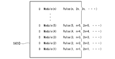
- the projection position of the second pulse corresponding to the second SLM (SLM (2)) shifts in the scanning direction as compared with the first pulse corresponding to the first SLM (SLM (1)).
- the projection position of the third pulse corresponding to the third SLM (SLM (3)) is further shifted in the scanning direction as compared with the second pulse corresponding to the second SLM (SLM (2)).
- the deviation of the projection position (exposure position) of the pattern is compensated even when the irradiation timing is different among the plurality of SLMs. ..
- the shapes, mounting positions, and / or postures of the plurality of SLMs are mechanically set so that the projected images from the plurality of SLMs have a predetermined positional relationship based on the deviation of the irradiation timing for the plurality of SLMs.
- the exposure apparatus is optically set so that the projected images from the plurality of SLMs have a predetermined positional relationship based on the deviation of the irradiation timing with respect to the plurality of SLMs.
- the position of the projected image on the substrate 1410 may be moved by adjusting the optical element in the projection optical system (projection lens) 1330, or the SLM may be moved with respect to the beam to move the position of the projected image on the substrate 1410. To do.
- the deviation of the projection position (exposure position) of the pattern is compensated.
- data corresponding to the projection positions sequentially shifted in the scanning direction is supplied to each of the plurality of SLMs.
- at least a part of the pattern data is corrected so that the projected images from the plurality of SLMs have a predetermined positional relationship based on the deviation of the irradiation timing with respect to the plurality of SLMs.
- the pattern data supplied to at least one of the plurality of SLMs includes correction data shifted in a predetermined direction with respect to the reference position, which is set based on the difference in irradiation timing.
- the pattern data includes the moving speed of the substrate stage 1400, the display update frequency of the SLM, the oscillation frequency of the laser beam, the rotation speed of the polygon mirror device (rotating device) 50 as a time divider, and the SLM60.
- the amount of shift in a predetermined direction with respect to the reference position may be determined based on at least one such as the number of (projection lenses 1330).
- the scanning direction (for example, the moving direction of the substrate stage) is switched between the + direction and the-direction (between one direction and the opposite direction) to expose one pattern on the substrate 1410.
- the pattern data supplied to the plurality of SLMs can be adjusted according to the scanning direction at the corresponding timing.
- the pattern data supplied to at least one of the plurality of SLMs includes the first correction data shifted in the + direction in the scanning direction with respect to the reference position and the first correction data shifted in the-direction in the scanning direction with respect to the reference position. 2 Includes correction data.
- the scanning direction for example, the moving direction of the substrate stage
- the scanning direction is switched between the + direction and the-direction (between one direction and the opposite direction).
- the exposure apparatus can be adjusted mechanically and / or optically at each timing of.
- the exposure apparatus (optical apparatus) 1000 can include a drive mechanism 1510 for mechanical adjustment and a drive mechanism 1520 for optical adjustment. Further, the exposure apparatus 1000 can include a database 1530 (or a storage unit) in which setting parameters and / or programs for data correction are stored. Such shift adjustment can be performed, for example, based on the output result of the reference system 1540 including the reference sensor and the like.
- the drive mechanism 1510 can be omitted if the attachment positions are staggered in advance. Further, even when the mounting positions of the SLMs are shifted in advance, the drive mechanism 1510 may be used in order to compensate for the mounting error.
- the control system 1500 uses the (a-1) drive mechanism 1510 for exposure based on the irradiation timings of the plurality of SLMs. Control at least one of mechanical adjustment of the apparatus 1000, (a-2) optical adjustment of the exposure apparatus 1000 using the drive mechanism 1520, and (a-3) correction of pattern data using the database 1530. be able to. For example, a shift adjustment that combines all of the above (a-1), (a-2), and (a-3) is executed. Alternatively, a shift adjustment based on one or a combination of one or two of the above (a-1), (a-2), and (a-3) is performed.
- pattern data correction is applied to relatively large shift adjustments and / or relatively coarse shift adjustments, and mechanical and / or optical adjustments are relatively small shift adjustments and / or relatively fine shifts. Applies to adjustments. In other examples, another method different from the above may be applied.
- the above shift adjustment can be performed based on the timing of beam use. Even when a predetermined period (for example, an unused pulse) occurs in which the beam is unused, the shift adjustment described above compensates for the deviation of the projection position (exposure position) of the pattern. For example, a beam during a relatively unstable period is eliminated and a stable beam is selectively used while avoiding a shift in the projection position of the pattern.
- a predetermined period for example, an unused pulse
- the exposure apparatus 1000 is arranged between a plurality of laser light sources 20, a plurality of output modules 30 having a plurality of SLMs 60, and a plurality of laser light sources 20 and an output module 30. It includes a polygon mirror device (rotating device) 50 as a time divider that temporally divides the combined laser beams emitted from the plurality of laser light sources 20.
- the beam from the laser light source 20 is reflected by each of the plurality of reflecting surfaces 52 of the polygon mirror 51 in the polygon mirror device 50.
- the beam is time-divided according to the rotation angle of the polygon mirror 51.
- the beam reflected by the polygon mirror 51 is distributed to the plurality of SLMs 60 via the plurality of optical fibers 80 according to the rotation angle of the polygon mirror 51.
- the time-division beam from the polygon mirror 51 is distributed to five SLM60s. For example, beams corresponding to the first pulse, the sixth pulse, and the like are incident on the first SLM. Beams corresponding to the second pulse, the seventh pulse, and the like are incident on the second SLM.
- the exposure apparatus 1000 is located between a plurality of laser light sources 20, a plurality of output modules 30 having a plurality of SLMs 60, and a plurality of laser light sources 20 and a plurality of output modules 30.
- the polygon mirror device (rotating device) 50 as a time divider that temporally divides the combined laser beam emitted from the plurality of laser light sources 20 and the plurality of laser light sources 20 and the polygon mirror device 50.
- the optical switch device 70 as a sub-divider 70 arranged in the above is provided.
- the beam from the optical switch device 70 is directed to the first position of the polygon mirror device 50 via the path "A" and is reflected by the polygon mirror 51 (reflection surface 52A).
- the beam from the optical switch device 70 is directed to the second position of the polygon mirror device 50 via the path "B” and is reflected by the polygon mirror 51 (reflection surface 52B).
- Beams are alternately supplied to the first position and the second position of the polygon mirror 51.
- the beam is further divided in time according to the rotation angle of the polygon mirror 51. That is, in this example, two time dividers are arranged in series along the optical path, and the beam is temporally divided into two stages.
- the time-division beam from the polygon mirror 51 is distributed to 10 SLM60s.
- beams corresponding to the first pulse, the eleventh pulse, and the like are incident on the first SLM.
- Beams corresponding to the second pulse, the twelfth pulse, and the like are incident on the second SLM.
- the beam reflected by the reflection surface 52A of the polygon mirror 51 is guided to the first SLM group (from the first SLM to the fifth SLM in FIG. 30), and the beam reflected by the reflection surface 52B is the first. It is led to 2 SLM groups (6th SLM to 10th SLM in FIG. 30).
- the exposure apparatus 1000 is located between a plurality of laser light sources 20, a plurality of output modules 30 having a plurality of SLMs 60, and a plurality of laser light sources 20 and a plurality of output modules 30.
- a plurality of polygon mirror devices (rotating devices) 50 as a time divider for temporally dividing a combined laser beam emitted from a plurality of laser light sources 20 and a plurality of laser light sources 20 and a plurality of polygon mirror devices. It includes an optical switch device 70 as a sub-divider arranged between the 50 and the 50.
- the plurality of polygon mirrors 51A and 51B of the plurality of polygon mirror devices 50 are arranged so as to be in a parallel positional relationship with respect to the optical path.
- the beam from the optical switch device 70 is directed toward the polygon mirror 51A in the first span on the time axis and is reflected by the reflecting surface of the polygon mirror 51A.
- the beam from the optical switch device 70 is directed toward the polygon mirror 51B and reflected by the reflecting surface of the polygon mirror 51B.
- the beam is further divided in time according to the rotation angles of the polygon mirrors 51A and 51B.
- the time-division beam from the polygon mirror 51A is distributed to five SLM60s.
- the time-division beam from the polygon mirror 51B is distributed to another five SLM60s.
- beams corresponding to the first pulse, the eleventh pulse, and the like are incident on the first SLM.
- Beams corresponding to the 6th pulse, the 16th pulse, and the like are incident on the 6th SLM.
- the beam reflected by the polygon mirror 51A is guided to the first SLM group (from the first SLM to the fifth SLM in FIG. 31), and the beam reflected by the polygon mirror 51B is the second SLM group. (In FIG. 30, the sixth SLM to the tenth SLM) is derived.
- the exposure apparatus 1000 is located between a plurality of laser light sources 20, a plurality of output modules 30 having a plurality of SLMs 60, and a plurality of laser light sources 20 and a plurality of output modules 30.
- a plurality of optical switch devices 50 as a time divider for temporally dividing a combined laser beam emitted from a plurality of laser light sources 20 and a plurality of laser light sources 20 and a plurality of optical switch polygon mirror devices 50. It includes an optical switch device 70 as a sub-divider arranged between the two.
- the plurality of optical members 55A, 55B, 55C of the plurality of optical switch devices 50 are arranged so as to have a positional relationship in parallel with respect to the optical path.
- the beam from the optical switch device 70 is directed toward the optical member 55A and is time-divisioned by the optical member 55A.
- the beam from the optical switch device 70 is directed toward the optical member 55B and is time-divisioned by the optical member 55B.
- the beam from the optical switch device 70 is directed toward the optical member 55C and is time-divisioned by the optical member 55C.
- the time-division beam from the optical member 55A is distributed to three SLM60s.
- the time-division beam from the optical member 55B is distributed to three other SLM60s.
- the time-division beam from the optical member 55C is distributed to three further SLM60s.
- beams corresponding to the first pulse, the tenth pulse, and the like are incident on the first SLM.
- Beams corresponding to the fourth pulse, the thirteenth pulse, and the like are incident on the fourth SLM.
- Beams corresponding to the 7th pulse, the 16th pulse, and the like are incident on the 7th SLM.
- the time-division beam in the optical member 55A is guided to the first SLM group (from the first SLM to the third SLM in FIG. 32), and the time-division beam in the optical member 55B is the second.
- the beam guided to the SLM group (4th SLM to 6th SLM in FIG. 32) and time-divisioned by the optical member 55C is the 3rd SLM group (7th SLM to 9th SLM in FIG. 32). ).
- the exposure apparatus 1000 includes a laser light source 20, a plurality of SLMs 60, and a plurality of polygon mirrors as a time divider arranged between the laser light source 20 and the plurality of SLMs 60s.
- the 51A, 51B, 51C and a plurality of optical switch devices 70 (optical members 75A, 75B) as sub-dividers arranged between the laser light source 20 and the plurality of polygon mirrors 51A, 51B, 51C are provided.
- the optical members 75A and 75B are rotating plates in which a reflection region and a transmission region are arranged side by side in the circumferential direction.
- the beam reflected by the optical member 75A in the first span on the time axis is directed toward the polygon mirror 51A and reflected by the reflecting surface of the polygon mirror 51.
- the beam transmitted through the optical member 75A and reflected by the optical member 75B in the second span on the time axis is directed toward the polygon mirror 51B and is reflected by the reflecting surface of the polygon mirror 51B.
- the beam transmitted through the optical member 75B in the third span on the time axis is directed toward the polygon mirror 51C and is reflected by the reflecting surface of the polygon mirror 51C.
- the beam is further divided in time according to the rotation angles of the polygon mirrors 51A, 51B, and 51C. A slight change in the incident angle of the beam based on the rotation of the polygon mirrors 51A-51C is advantageous in suppressing the speckle.
- the exposure apparatus 1000 serves as a time divider arranged between the plurality of laser light sources 20, the plurality of SLMs 60, and the plurality of laser light sources 20 and the plurality of SLMs 60s.
- a plurality of optical switch devices 70 (optical) as sub-dividers arranged between a plurality of polygon mirrors 51A, 51B, 51C, 51D, 51E, 51F and a plurality of laser light sources 20 and a plurality of polygon mirrors 51A-51F.
- the optical members 75A-75F are AOMs (acousto-optic modulators).
- the beam branched by the optical member 75C heads toward the polygon mirror 51C, and the beam branched by the optical member 75F heads toward the polygon mirror 51F.
- the beam branched by the optical member 75B heads toward the polygon mirror 51B, and the beam branched by the optical member 75E heads toward the polygon mirror 51E.
- the beam branched by the optical member 75A heads toward the polygon mirror 51A, and the beam branched by the optical member 75D heads toward the polygon mirror 51D.
- the beam is further divided in time according to the rotation angle of the polygon mirrors 51A-51F. A slight change in the incident angle of the beam based on the rotation of the polygon mirrors 51A-51F is advantageous in suppressing the speckle.
- the substrate 1410 is sequentially exposed by beams from a plurality of output modules according to the timing of pulse emission. That is, based on the beams from the plurality of output modules (1, 2, 3, ... n), a plurality of patterns are sequentially projected onto the substrate 1410 according to the timing of pulse emission.
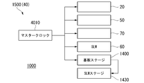
- the exposure apparatus 1000 includes a master clock (oscillator that emits a master clock) 4010 that serves as a reference for synchronization.
- a master clock oscillator that emits a master clock
- Each device is driven with reference to the master clock 4010.
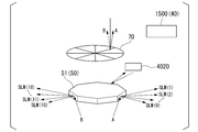
- each device is provided with an origin sensor 4020 as needed.
- the control system 1500 acquires information regarding the rotation of the polygon mirror 51 based on the output data from the origin sensor 4020.
- the control system 1500 can control each device based on the information from each device and the information from the master clock 4010.
- the control system 1500 adjusts the rotation speed of the polygon mirror 51 so as to match the clock frequency of the master clock 4010 based on the rotation information of the polygon mirror 51. Further, the control system 1500 adjusts the phase of the polygon mirror 51 so as to match the clock timing of the master clock 4010. As a result, the polygon mirror 51 is rotated and controlled in synchronization with the master clock 4010.
- the sub-divider (optical switch device 70) (FIG. 36) can be adjusted in the same manner.
- control system 1500 can control the trigger signal of the image display start in the SLM 60 with reference to the master clock 4010, that is, the image update frequency can be controlled.
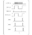
- the control system 1500 can control the operation of the substrate stage 1400 that supports the substrate with reference to the master clock 4010. Further, the control system 1500 can control the operation of the SLM stage 1430 that supports the SLM 60 so that the positional deviation from the substrate stage 1400 is eliminated. By operating the SLM stage 1430, the position of the projected image projected on the substrate 1410 can be moved as described above. With reference to the master clock 4010, as shown in FIG. 39, the operation timing of each device is appropriately adjusted individually, and the relationship between the operation timings of the plurality of devices is appropriately set.
- the emitted beam may become unstable.
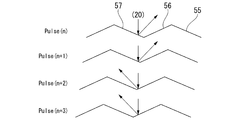
- the rotating plate 55 shown in FIG. 9B when the beam is incident on the top or bottom located at the boundary between the first reflecting surface 56 and the second reflecting surface 57, the reflected beam is generated. It may be scattered or the beam may be distorted.
- the boundary between the first reflecting surface 56 and the second reflecting surface 57 on the rotating plate 55 is formed by appropriately controlling the rotation of the rotating plate 55 according to the oscillation timing of the laser light source 20.
- the incident of the beam on the part is avoided.
- the optical boundary (top or bottom) of the rotating plate 55 is located at the target irradiation position of the beam.
- the rotation of the rotating plate 55 is controlled. This improves the utilization efficiency of the beam.
- the optical boundaries for division in the time divider 50 may be processed differently from other regions.
- additional processing is performed near the boundary (near the bottom) between the first reflecting surface 56 and the second reflecting surface 57 on the rotating plate 55.
- relatively high-precision additional processing is performed near the boundary of the rotating plate 55. Beam utilization efficiency is improved based on high surface accuracy in the region near the optical boundary.
- steps 55A and 55B are formed as marks of additional machining near the boundary (near the bottom) between the first reflecting surface 56 and the second reflecting surface 57 on the rotating plate 55.
- the rotation of the rotating plate 55 is controlled so that the step 55A on the rotating plate 55 is located at the target irradiation position of the beam at the timing between the (n) th pulse and the (n + 1) th pulse. ..
- the rotation of the rotating plate 55 is controlled so that the step 55B on the rotating plate 55 is located at the target irradiation position of the beam at the timing between the (n + 2) th pulse and the (n + 3) th pulse. ..
- the exposure apparatus (1000) that exposes a predetermined pattern on the substrate spatially modulates the light source (20) and the light from the light source (20) based on the pattern data that describes the predetermined pattern.
- the spatial light modulator (60), the projection optical system (1330) that projects the spatially modulated projection image of the light onto the substrate, and the optical path of the light oscillated sequentially from the light source (20) are switched.
- the optical path switching machine (50, 70) for switching the optical path of the light is provided so as to guide the light path to the spatial modulators (60) provided in order, and the optical path switching device (50, 70) sets the optical path.
- a first switching machine (70) that switches between the first optical path and the second optical path, and a spatial optical modulator of the first group among a plurality of spatial optical modulators that transfer the light guided to the first optical path to either one of the first optical path and the second optical path.
- a second switching machine (50) that guides the light guided to the second optical path to the second group of spatial modulators (60) among the plurality of spatial light modulators, and a second switching device (50).
- the first switching machine (70) has a first region that guides the light oscillated from the light source (20) within the first period to the first optical path, and the first region from the light source (20). It has a second region that guides the light oscillated within a second period different from the period to the second optical path.
- the first region reflects the light
- the second region transmits the light
- the first region is provided at an angle of a first angle with respect to the light, reflects the light and guides the light to the first optical path
- the second region is the light with respect to the light. It is provided at an inclination of a second angle different from the first angle, reflects the light, and guides the light to the second optical path.
- the second switching machine (50) has a first reflecting surface (52A) that reflects the light to the spatial light modulator (60) of the first group and a spatial light modulation of the second group. It has a second reflecting surface (52B) that guides the light back to the vessel (60).
- the second switching machine (50) includes a first switching machine (50, 51A) that guides the light to the spatial light modulator (60) of the first group and a spatial light modulator (60) of the second group. It has a second switching machine (50, 51B) that guides the light to the head.
- the exposure apparatus (1000) comprises a data transmitter (1500) that transmits the pattern data to the spatial light modulator (60), wherein the spatial light modulator (60). It has a first spatial light modulator (60) and a second spatial light modulator (60) provided side by side in a second direction intersecting the first direction in which the substrate is moved during exposure.
- the data transmission unit (1500) transmits the pattern data to the first spatial light modulator (60) and the second pattern data transmitted to the second spatial light modulator (60). It is divided into data, and the positions of the first pattern data and the second pattern data in the first direction are relatively shifted.
- the exposure apparatus (1000) comprises a data transmitter (1500) that transmits the pattern data to the spatial light modulator (60), wherein the spatial light modulator (60) , A first spatial light modulator (60) and a second spatial light modulator (60), and the data transmission unit (1500) transfers the pattern data to the first spatial light modulator (60).
- the first pattern data to be transmitted and the second pattern data to be transmitted to the second spatial light modulator (60) are divided, and the positions of the first pattern data and the second pattern data are relatively relative to each other. Shift.
- the second switching machine (50) is a polygon mirror.
- the exposure apparatus (1000) is a first spatial light modulator (60) arranged side by side in a second direction intersecting the first direction with respect to a substrate moving in the first direction.
- a predetermined pattern is exposed via the second light modulator (60).
- the exposure apparatus (1000) transmits the light source (20) and the pattern data described based on the predetermined pattern to the first spatial light modulator (60) and the second spatial light modulator (60).
- the light from the transmission unit (1500) and the light source (20) is a part of the pattern data, and the first spatial modulator (60) is based on the first pattern data transmitted by the transmission unit (1500).
- the first projection optical system (1330) that projects the projection image of the light spatially modulated by () onto the substrate, and the light from the light source (20) are other parts of the pattern data and the transmission part (
- Optical path switching that switches the optical path of light sequentially oscillated from the optical system (1330) and the light source (20) and guides the first spatial modulator (60) and the second spatial modulator (60) in this order.
- a machine (50) is provided, and the data transmission unit (1500) divides the pattern data into the first pattern data and the second pattern data, and divides the pattern data into the first pattern data and the second pattern data.
- the position with respect to the data in the first direction is relatively shifted.
- the exposure apparatus (1000) is an oscillator (4010) that emits a master clock that synchronizes at least two of the light source (20), the spatial light modulator (60), and the optical path switcher (50). To be equipped.
- the exposure apparatus further includes a synthesizer (1200) that synthesizes the light emitted from each of the plurality of light sources (20), and the optical path switching device (50) synthesizes the light by the synthesizer (1200). The optical path of the light is switched.
- a synthesizer (1200) that synthesizes the light emitted from each of the plurality of light sources (20)
- the optical path switching device (50) synthesizes the light by the synthesizer (1200). The optical path of the light is switched.
- the method for manufacturing a flat panel display includes exposing the substrate using the exposure apparatus (1000) and developing the exposed substrate.
- the device manufacturing method includes exposing the substrate using the exposure apparatus (1000) and developing the exposed substrate.
- the exposure apparatus 1000 can also be used, for example, as a semiconductor photolithography system that exposes an integrated circuit pattern on a wafer or a photolithography system that manufactures a thin film magnetic head.
- a low frequency and high energy beam output can be realized by combining a plurality of beams and time division, but the present invention is not limited to this.
- a high-energy beam is output from a laser light source, it is not necessary to combine multiple beams.
- the combination of multiple beams includes the case where the optical axes of the laser beams emitted from the multiple light sources match and are combined. In addition, even if the optical axes of the laser beams emitted from multiple light sources do not match, if the optical axes are close enough, a high-energy beam output may be obtained or the beams may be combined. Including.
- the above-mentioned photolithography system can be constructed by assembling various subsystems so that predetermined mechanical accuracy, electrical accuracy, and optical accuracy are maintained. To maintain varying accuracy before and after assembly, each optical system is tuned to achieve its optical accuracy. Similarly, all mechanical and electrical systems are tuned to achieve mechanical and electrical accuracy.
- the process of assembling each subsystem into a photolithography system includes mechanical interfaces, electrical circuit wiring connections, and pneumatic piping connections between each subsystem. There is also a process of assembling each subsystem prior to assembling the photolithography system from the various subsystems. Once the photolithography system is assembled using the various subsystems, all adjustments are made to ensure accuracy in the complete photolithography system. Further, it is desirable to manufacture the exposure system in a clean room where the temperature and cleanliness are controlled.
- the substrate to be exposed is not limited to the glass plate, and may be another object such as a wafer, a ceramic substrate, a film member, or a mask blank.
- the thickness of the substrate is not particularly limited, and for example, a film-like (flexible sheet-like member) is also included.
- the exposure apparatus of the present embodiment is particularly effective when a substrate having a side length or a diagonal length of 500 mm or more is an exposure target.
- the lithography step of transferring the mask (reticle) pattern to the glass substrate by the exposure method the developing step of developing the exposed glass substrate, and the portion where the resist remains. It is manufactured through an etching step of removing exposed members by etching, a resist removing step of removing a resist that is no longer needed after etching, a device assembly step, an inspection step, and the like.
- the above-mentioned exposure method is executed using the exposure apparatus of the above embodiment, and the device pattern is formed on the glass substrate, so that a device having a high degree of integration can be manufactured with high productivity. ..
- 20 Laser light source, 30: Output module, 40: Controller, 50: Time divider, 51: Polygon mirror, 60: Spatial light modulator (SLM), 70: Subdivider, 80: Optical fiber, 1000: Exposure device (Optical device), 1100: Light source module, 1200: Distribution module, 1300: Lighting system, 1310: Lighting system, 1330: Projection lens, 1400: Board stage, 1410: Board, 1500: Control system
Landscapes
- Physics & Mathematics (AREA)
- Optics & Photonics (AREA)
- Engineering & Computer Science (AREA)
- Plasma & Fusion (AREA)
- Mechanical Engineering (AREA)
- General Physics & Mathematics (AREA)
- Nonlinear Science (AREA)
- Manufacturing & Machinery (AREA)
- Crystallography & Structural Chemistry (AREA)
- Chemical & Material Sciences (AREA)
- Exposure And Positioning Against Photoresist Photosensitive Materials (AREA)
- Mechanical Optical Scanning Systems (AREA)
- Lasers (AREA)
- Mechanical Light Control Or Optical Switches (AREA)
- Optical Modulation, Optical Deflection, Nonlinear Optics, Optical Demodulation, Optical Logic Elements (AREA)
- Liquid Crystal (AREA)
- Semiconductor Lasers (AREA)
- Optical Radar Systems And Details Thereof (AREA)
- Laser Beam Printer (AREA)
Abstract
Description
本願は、2020年1月10日に出願された米国特許仮出願第62/959,178号に基づき優先権を主張し、その内容をここに援用する。
Claims (27)
- 複数のレーザ光源と、
光変調器を有する出力モジュールと、
前記複数のレーザ光源と前記出力モジュールとの間に配され、前記複数のレーザ光源から出射されたレーザ光を時間的に分割する時分割器と、
を備える、光学装置。 - 複数のレーザ光源と、
各々が光変調器を有する複数の出力モジュールと、
前記複数のレーザ光源と前記複数の出力モジュールとの間に配され、前記複数のレーザ光源から出射されたレーザ光を時間的に分割する時分割器と、
を備える、光学装置。 - 複数のレーザ光源と、
各々が光変調器を有する複数の出力モジュールと、
前記複数のレーザ光源と前記複数の出力モジュールとの間に配され、前記複数のレーザ光源から出射されたレーザ光を時間的に分割する時分割器と、
前記複数のレーザ光源と前記時分割器との間、又は前記時分割器と前記複数の出力モジュールとの間、に配される副分割器と、
を備える、光学装置。 - レーザ光源と、
出力モジュールと、
前記レーザ光源と前記出力モジュールとの間に配され、前記レーザ光源から出射されたレーザ光を時間的に分割する時分割器と、
を備え、
前記時分割器は、複数の反射面を用いて前記レーザ光を分割する、
光学装置。 - レーザ光源と、
複数の出力モジュールと、
前記レーザ光源と前記複数の出力モジュールとの間に配され、前記レーザ光源から出射されたレーザ光を時間的に分割する時分割器と、
を備え、
前記時分割器は、複数の反射面を用いて前記レーザ光を分割する、
光学装置。 - 前記レーザ光源を複数備える、請求項4または5に記載の光学装置。
- レーザ光源と、
光変調器を有する出力モジュールと、
前記光源と前記出力モジュールとの間に配された音響光学素子と、
を備える、光学装置。 - レーザ光源と、
各々が光変調器を有する複数の出力モジュールと、
前記レーザ光源と前記出力モジュールとの間に配された音響光学素子と、
を備える、光学装置。 - 前記レーザ光源を複数備える、請求項7または8に記載の光学装置。
- パルス光を出射するレーザ光源と、
光変調器を有する出力モジュールと、
前記レーザ光源と前記出力モジュールとの間に配され、前記パルス光を時間的に分割する時分割器と、
前記パルス光の周波数に基づいて、前記時分割器による前記パルス光の分割を制御するコントローラと、
を備える、光学装置。 - パルス光を出射するレーザ光源と、
各々が光変調器を有する複数の出力モジュールと、
前記レーザ光源と前記複数の出力モジュールとの間に配され、前記パルス光を時間的に分割する時分割器と、
前記パルス光の周波数に基づいて、前記時分割器による前記パルス光の分割を制御するコントローラと、
を備える、光学装置。 - 前記レーザ光源を複数備える、請求項10または11に記載の光学装置。
- 請求項1から12の何れか一項に記載の光学装置と、
前記光変調器により導かれる光により露光される基板を支持する基板支持部と、を備える露光装置。 - 基板上に所定パターンを露光する露光装置において、
光源と、
前記光源からの前記光を、前記所定パターンを記述したパターンデータに基づいて空間変調する空間光変調器と、
前記空間変調された前記光の投影像を前記基板へ投影する投影光学系と、
前記光源から順次発振された光の光路を切り替えて、複数設けられた前記空間変調器に順に導く光路切替え機と、を備え、
前記光路切替え機は、前記光路を第1光路と第2光路とのどちらか一方へ切り替える第1切替え機と、前記第1光路へ導かれた前記光を複数の空間光変調器のうち第1群の空間光変調器へ、前記第2光路へ導かれた前記光を複数の空間光変調器のうち第2群の空間変調器へ、前記光をそれぞれ導く第2切替え機と、を有する、露光装置。 - 前記第1切替え機は、前記光源から第1期間内に発振された前記光を前記第1光路へ導く第1領域と、前記光源から前記第1期間とは異なる第2期間内に発振された前記光を前記第2光路へ導く第2領域と、を有する、請求項14に記載の露光装置。
- 前記第1領域は、前記光を反射し、
前記第2領域は、前記光を透過する、請求項15に記載の露光装置。 - 前記第1領域は、前記光に対して第1角度に傾けて設けられ、前記光を反射して前記光を前記第1光路へ導き、
前記第2領域は、前記光に対して前記第1角度とは異なる第2角度に傾けて設けられ、前記光を反射して前記光を前記第2光路へ導く、請求項15に記載の露光装置。 - 前記第2切替え機は、前記第1群の空間光変調器へ前記光を反射させる第一反射面と、前記第2群の空間光変調器へ前記光を反射させる導く第二反射面と、を有する、請求項14から17の何れか一項に記載の露光装置。
- 前記第2切替え機は、前記第1群の空間光変調器へ前記光を導く第一切替え機と、前記第2群の空間光変調器へ前記光を導く第二切替え機と、を有する、請求項14から17の何れか一項に記載の露光装置。
- 前記パターンデータを前記空間光変調器へ送信するデータ送信部、を備え、
前記空間光変調器は、露光中に前記基板が移動される第1方向と交差する第2方向に複数並んで設けられた第1空間光変調器と第2空間光変調器とを有し、
前記データ送信部は、前記パターンデータを、前記第1空間光変調器へ送信される第1パターンデータと、前記第2空間光変調器へ送信される第2パターンデータとに分割し、前記第1パターンデータと前記第2パターンデータとの前記第1方向に関する位置を相対的にシフトさせる、請求項14から19の何れか一項に記載の露光装置。 - 前記パターンデータを前記空間光変調器へ送信するデータ送信部、を備え、
前記空間光変調器は、第1空間光変調器と第2空間光変調器とを有し、
前記データ送信部は、前記パターンデータを、前記第1空間光変調器へ送信される第1パターンデータと、前記第2空間光変調器へ送信される第2パターンデータとに分割し、前記第1パターンデータと前記第2パターンデータとの位置を相対的にシフトさせる、請求項14から19の何れか一項に記載の露光装置。 - 前記第2切替え機は、ポリゴンミラーである、請求項14から21の何れか一項に記載の露光装置。
- 第1方向へ移動中の基板に対して、前記第1方向と交差する第2方向に並んで配置された第1空間光変調器と前記第2光変調器とを介して、所定パターンを露光する露光装置において、
光源と、
前記所定パターンに基づいて記述されるパターンデータを前記第1空間光変調器および前記第2空間光変調器へ送信するデータ送信部、
前記光源からの前記光が、前記パターンデータの一部であり前記送信部により送信された第1パターンデータに基づいて前記第1空間変調器により空間変調された前記光の投影像を前記基板へ投影する第1投影光学系と、
前記光源からの前記光が、前記パターンデータの他部であり前記送信部により送信された第2パターンデータに基づいて空間変調する第2の空間光変調器と、
前記第2の空間変調された前記光の投影像を前記基板へ投影する第2投影光学系と、
前記光源から順次発振された光の光路を切り替えて、前記第1の空間変調器、前記第2の空間変調器の順に導く光路切替え機と、を備え、
前記データ送信部は、前記パターンデータを、前記第1パターンデータと、前記第2パターンデータとに分割し、前記第1パターンデータと前記第2パターンデータとの前記第1方向に関する位置を相対的にシフトさせる、露光装置。 - 前記光源と、前記空間光変調器と、前記光路切替え機との少なくとも2つを同期させるマスタークロックを発する発振器を備える、請求項14から23の何れか一項に記載の露光装置。
- 複数の前記光源からそれぞれ発せられた前記光を合成する合成器を、さらに備え、
前記光路切替え機は、前記合成器により合成された前記光の前記光路を切り替える、請求項14から24の何れか一項に記載の露光装置。 - 請求項13から25の何れか一項に記載の露光装置を用いて前記基板を露光することと、露光された前記基板を現像することと、を含むフラットパネルディスプレイの製造方法。
- 請求項13から25の何れか一項に記載の露光装置を用いて前記基板を露光することと、
露光された前記基板を現像することと、を含むデバイス製造方法。
Priority Applications (11)
| Application Number | Priority Date | Filing Date | Title |
|---|---|---|---|
| KR1020257031304A KR20250141846A (ko) | 2020-01-10 | 2021-01-08 | 광학 장치, 노광 장치, 플랫 패널 디스플레이의 제조 방법, 및 디바이스 제조 방법 |
| CN202512039153.8A CN121763667A (zh) | 2020-01-10 | 2021-01-08 | 光学装置、曝光装置及器件制造方法 |
| JP2021570119A JP7416090B2 (ja) | 2020-01-10 | 2021-01-08 | 光学装置、露光装置、フラットパネルディスプレイの製造方法、及びデバイス製造方法 |
| EP21738415.5A EP4089485A4 (en) | 2020-01-10 | 2021-01-08 | OPTICAL DEVICE, EXPOSURE DEVICE, METHOD FOR MANUFACTURING FLAT SCREEN AND METHOD FOR MANUFACTURING DEVICE |
| KR1020227025942A KR102878468B1 (ko) | 2020-01-10 | 2021-01-08 | 광학 장치, 노광 장치, 플랫 패널 디스플레이의 제조 방법, 및 디바이스 제조 방법 |
| CN202180012073.0A CN115023663B (zh) | 2020-01-10 | 2021-01-08 | 曝光装置、平板显示器的制造方法及电子器件制造方法 |
| US17/859,140 US11899372B2 (en) | 2020-01-10 | 2022-07-07 | Optical device, exposure device, method for manufacturing flat panel display, and method for manufacturing device |
| JP2023214782A JP7622805B2 (ja) | 2020-01-10 | 2023-12-20 | 光学装置、及びデバイス製造方法 |
| US18/400,139 US12248253B2 (en) | 2020-01-10 | 2023-12-29 | Optical device, exposure device, method for manufacturing flat panel display, and method for manufacturing device |
| JP2025002338A JP2025061072A (ja) | 2020-01-10 | 2025-01-07 | 露光装置 |
| US19/039,068 US20250170671A1 (en) | 2020-01-10 | 2025-01-28 | Optical device, exposure device, method for manufacturing flat panel display, and method for manufacturing device |
Applications Claiming Priority (2)
| Application Number | Priority Date | Filing Date | Title |
|---|---|---|---|
| US202062959178P | 2020-01-10 | 2020-01-10 | |
| US62/959,178 | 2020-01-10 |
Related Child Applications (1)
| Application Number | Title | Priority Date | Filing Date |
|---|---|---|---|
| US17/859,140 Continuation US11899372B2 (en) | 2020-01-10 | 2022-07-07 | Optical device, exposure device, method for manufacturing flat panel display, and method for manufacturing device |
Publications (1)
| Publication Number | Publication Date |
|---|---|
| WO2021141128A1 true WO2021141128A1 (ja) | 2021-07-15 |
Family
ID=76787987
Family Applications (1)
| Application Number | Title | Priority Date | Filing Date |
|---|---|---|---|
| PCT/JP2021/000578 Ceased WO2021141128A1 (ja) | 2020-01-10 | 2021-01-08 | 光学装置、露光装置、フラットパネルディスプレイの製造方法、及びデバイス製造方法 |
Country Status (7)
| Country | Link |
|---|---|
| US (3) | US11899372B2 (ja) |
| EP (1) | EP4089485A4 (ja) |
| JP (3) | JP7416090B2 (ja) |
| KR (2) | KR102878468B1 (ja) |
| CN (2) | CN115023663B (ja) |
| TW (2) | TW202526523A (ja) |
| WO (1) | WO2021141128A1 (ja) |
Cited By (1)
| Publication number | Priority date | Publication date | Assignee | Title |
|---|---|---|---|---|
| WO2025197436A1 (ja) * | 2024-03-19 | 2025-09-25 | 株式会社ニコン | 露光方法、露光装置、及びデバイス製造方法 |
Families Citing this family (4)
| Publication number | Priority date | Publication date | Assignee | Title |
|---|---|---|---|---|
| KR102878468B1 (ko) * | 2020-01-10 | 2025-10-29 | 가부시키가이샤 니콘 | 광학 장치, 노광 장치, 플랫 패널 디스플레이의 제조 방법, 및 디바이스 제조 방법 |
| KR20230024468A (ko) * | 2021-08-11 | 2023-02-21 | 삼성전자주식회사 | 레이저 어닐링 장치 및 그것의 동작 방법 |
| DE102023123551B4 (de) | 2023-08-31 | 2025-03-13 | Nanoscribe Holding Gmbh | Verfahren zum Erzeugen einer dreidimensionalen Struktur und Laserlithografie-Vorrichtung |
| DE102023123552A1 (de) * | 2023-08-31 | 2025-03-06 | Nanoscribe Holding Gmbh | Laserlithografie-Vorrichtung zum Erzeugen einer dreidimensionalen Struktur und Verfahren zum Betreiben einer Laserlithografie-Vorrichtung |
Citations (13)
| Publication number | Priority date | Publication date | Assignee | Title |
|---|---|---|---|---|
| US6552775B1 (en) | 1999-11-26 | 2003-04-22 | Nikon Corporation | Exposure method and apparatus |
| JP2004245911A (ja) * | 2003-02-12 | 2004-09-02 | Pentax Corp | パターン描画装置 |
| JP2006049635A (ja) * | 2004-08-05 | 2006-02-16 | Sumitomo Heavy Ind Ltd | レーザ照射方法及びレーザ照射装置並びにレーザアニール方法 |
| JP2006191063A (ja) * | 2004-12-29 | 2006-07-20 | Asml Netherlands Bv | リソグラフィ・ビーム形成方法及びシステム |
| US20090117494A1 (en) | 2007-11-06 | 2009-05-07 | Nikon Corporation | Controller for optical device, exposure method and apparatus, and method for manufacturing device |
| JP2009521108A (ja) * | 2005-12-21 | 2009-05-28 | マイクロニック レーザー システムズ アクチボラゲット | Slm直接描画装置 |
| US20100099049A1 (en) | 2007-07-13 | 2010-04-22 | Nikon Corporation | Pattern forming method and apparatus, exposure method and apparatus, and device manufacturing method and device |
| US20130222781A1 (en) | 2010-09-27 | 2013-08-29 | Nikon Corporation | Method for driving spatial light modulator, method for forming pattern for exposure, exposure method, and exposure apparatus |
| US20130278912A1 (en) | 2010-09-22 | 2013-10-24 | Nikon Corporation | Spatial light modulator, exposure apparatus, and method for manufacturing device |
| US20130314683A1 (en) | 2010-12-13 | 2013-11-28 | Yoji Watanabe | Spatial light modulator, method of driving same, and exposure method and apparatus |
| US20140320835A1 (en) | 2011-09-02 | 2014-10-30 | Nikon Corporation | Method and device for inspecting spatial light modulator, and exposure method and device |
| US20150077732A1 (en) | 2012-01-18 | 2015-03-19 | Nikon Corporation | Drive method for spatial light modulator, method for generating pattern for exposure, and exposure method and apparatus |
| JP2017142526A (ja) * | 2011-08-19 | 2017-08-17 | オルボテック リミテッド | ダイレクトイメージングシステムおよび方法 |
Family Cites Families (22)
| Publication number | Priority date | Publication date | Assignee | Title |
|---|---|---|---|---|
| US4820899A (en) | 1987-03-03 | 1989-04-11 | Nikon Corporation | Laser beam working system |
| JPH0770459B2 (ja) * | 1987-03-03 | 1995-07-31 | 株式会社ニコン | 露光装置及び半導体製造装置 |
| WO2001014924A1 (en) * | 1999-08-26 | 2001-03-01 | The Ohio State University | Device for producing optically-controlled incremental time delays |
| JP2001133710A (ja) | 1999-11-05 | 2001-05-18 | Asahi Optical Co Ltd | マルチヘッド走査光学系を持つレーザ描画装置 |
| SG111171A1 (en) * | 2002-11-27 | 2005-05-30 | Asml Netherlands Bv | Lithographic projection apparatus and device manufacturing method |
| US6870554B2 (en) * | 2003-01-07 | 2005-03-22 | Anvik Corporation | Maskless lithography with multiplexed spatial light modulators |
| US7190434B2 (en) * | 2004-02-18 | 2007-03-13 | Asml Netherlands B.V. | Lithographic apparatus and device manufacturing method |
| US20050212722A1 (en) * | 2004-03-26 | 2005-09-29 | Schroeder Dale W | Spatial light modulator and method for interleaving data |
| CN100517069C (zh) * | 2004-08-05 | 2009-07-22 | 中国科学院光电技术研究所 | 用两个正交声光调制器的成像干涉光刻方法及光刻系统 |
| KR20090023545A (ko) * | 2006-05-31 | 2009-03-05 | 가부시키가이샤 니콘 | 노광 장치 및 노광 방법 |
| JP4921159B2 (ja) * | 2006-12-28 | 2012-04-25 | キヤノン株式会社 | 光ビーム走査装置 |
| JP5090780B2 (ja) * | 2007-04-26 | 2012-12-05 | 株式会社オーク製作所 | 露光描画装置 |
| CN102207690A (zh) * | 2011-05-20 | 2011-10-05 | 合肥芯硕半导体有限公司 | 一种多slm曝光和数据处理方法 |
| US8477403B2 (en) * | 2011-08-24 | 2013-07-02 | Palo Alto Research Center Incorporated | Variable length imaging apparatus using electronically registered and stitched single-pass imaging systems |
| CN102566312A (zh) * | 2012-01-13 | 2012-07-11 | 合肥芯硕半导体有限公司 | 无掩膜直写式光刻机系统中图形数据灰度值的计算方法 |
| CN105242497B (zh) * | 2015-09-09 | 2017-05-24 | 合肥芯碁微电子装备有限公司 | 具有抗拼接撕裂用于激光直写成像设备的扫描曝光方法 |
| KR102380603B1 (ko) * | 2016-03-30 | 2022-03-31 | 가부시키가이샤 니콘 | 패턴 묘화 장치, 패턴 묘화 방법, 및 디바이스 제조 방법 |
| JP6818479B2 (ja) * | 2016-09-16 | 2021-01-20 | デクセリアルズ株式会社 | 原盤の製造方法 |
| WO2018164087A1 (ja) * | 2017-03-10 | 2018-09-13 | 株式会社ニコン | パターン描画装置、及びパターン露光装置 |
| WO2019064511A1 (ja) * | 2017-09-29 | 2019-04-04 | 株式会社ニコン | 電子ビーム装置及びデバイス製造方法 |
| CN109407471B (zh) * | 2018-11-26 | 2021-07-16 | 合肥芯碁微电子装备股份有限公司 | 一种直写光刻设备的位置同步方法及系统 |
| KR102878468B1 (ko) * | 2020-01-10 | 2025-10-29 | 가부시키가이샤 니콘 | 광학 장치, 노광 장치, 플랫 패널 디스플레이의 제조 방법, 및 디바이스 제조 방법 |
-
2021
- 2021-01-08 KR KR1020227025942A patent/KR102878468B1/ko active Active
- 2021-01-08 CN CN202180012073.0A patent/CN115023663B/zh active Active
- 2021-01-08 CN CN202512039153.8A patent/CN121763667A/zh active Pending
- 2021-01-08 EP EP21738415.5A patent/EP4089485A4/en active Pending
- 2021-01-08 TW TW114111067A patent/TW202526523A/zh unknown
- 2021-01-08 WO PCT/JP2021/000578 patent/WO2021141128A1/ja not_active Ceased
- 2021-01-08 JP JP2021570119A patent/JP7416090B2/ja active Active
- 2021-01-08 TW TW110100867A patent/TWI881014B/zh active
- 2021-01-08 KR KR1020257031304A patent/KR20250141846A/ko active Pending
-
2022
- 2022-07-07 US US17/859,140 patent/US11899372B2/en active Active
-
2023
- 2023-12-20 JP JP2023214782A patent/JP7622805B2/ja active Active
- 2023-12-29 US US18/400,139 patent/US12248253B2/en active Active
-
2025
- 2025-01-07 JP JP2025002338A patent/JP2025061072A/ja active Pending
- 2025-01-28 US US19/039,068 patent/US20250170671A1/en active Pending
Patent Citations (13)
| Publication number | Priority date | Publication date | Assignee | Title |
|---|---|---|---|---|
| US6552775B1 (en) | 1999-11-26 | 2003-04-22 | Nikon Corporation | Exposure method and apparatus |
| JP2004245911A (ja) * | 2003-02-12 | 2004-09-02 | Pentax Corp | パターン描画装置 |
| JP2006049635A (ja) * | 2004-08-05 | 2006-02-16 | Sumitomo Heavy Ind Ltd | レーザ照射方法及びレーザ照射装置並びにレーザアニール方法 |
| JP2006191063A (ja) * | 2004-12-29 | 2006-07-20 | Asml Netherlands Bv | リソグラフィ・ビーム形成方法及びシステム |
| JP2009521108A (ja) * | 2005-12-21 | 2009-05-28 | マイクロニック レーザー システムズ アクチボラゲット | Slm直接描画装置 |
| US20100099049A1 (en) | 2007-07-13 | 2010-04-22 | Nikon Corporation | Pattern forming method and apparatus, exposure method and apparatus, and device manufacturing method and device |
| US20090117494A1 (en) | 2007-11-06 | 2009-05-07 | Nikon Corporation | Controller for optical device, exposure method and apparatus, and method for manufacturing device |
| US20130278912A1 (en) | 2010-09-22 | 2013-10-24 | Nikon Corporation | Spatial light modulator, exposure apparatus, and method for manufacturing device |
| US20130222781A1 (en) | 2010-09-27 | 2013-08-29 | Nikon Corporation | Method for driving spatial light modulator, method for forming pattern for exposure, exposure method, and exposure apparatus |
| US20130314683A1 (en) | 2010-12-13 | 2013-11-28 | Yoji Watanabe | Spatial light modulator, method of driving same, and exposure method and apparatus |
| JP2017142526A (ja) * | 2011-08-19 | 2017-08-17 | オルボテック リミテッド | ダイレクトイメージングシステムおよび方法 |
| US20140320835A1 (en) | 2011-09-02 | 2014-10-30 | Nikon Corporation | Method and device for inspecting spatial light modulator, and exposure method and device |
| US20150077732A1 (en) | 2012-01-18 | 2015-03-19 | Nikon Corporation | Drive method for spatial light modulator, method for generating pattern for exposure, and exposure method and apparatus |
Non-Patent Citations (1)
| Title |
|---|
| See also references of EP4089485A4 |
Cited By (1)
| Publication number | Priority date | Publication date | Assignee | Title |
|---|---|---|---|---|
| WO2025197436A1 (ja) * | 2024-03-19 | 2025-09-25 | 株式会社ニコン | 露光方法、露光装置、及びデバイス製造方法 |
Also Published As
| Publication number | Publication date |
|---|---|
| JP2024050536A (ja) | 2024-04-10 |
| TW202144921A (zh) | 2021-12-01 |
| US20250170671A1 (en) | 2025-05-29 |
| US20230004094A1 (en) | 2023-01-05 |
| KR20220122705A (ko) | 2022-09-02 |
| US12248253B2 (en) | 2025-03-11 |
| EP4089485A4 (en) | 2024-02-14 |
| KR102878468B1 (ko) | 2025-10-29 |
| JPWO2021141128A1 (ja) | 2021-07-15 |
| KR20250141846A (ko) | 2025-09-29 |
| CN115023663A (zh) | 2022-09-06 |
| EP4089485A1 (en) | 2022-11-16 |
| TWI881014B (zh) | 2025-04-21 |
| US20240134288A1 (en) | 2024-04-25 |
| JP7416090B2 (ja) | 2024-01-17 |
| JP2025061072A (ja) | 2025-04-10 |
| CN121763667A (zh) | 2026-03-31 |
| TW202526523A (zh) | 2025-07-01 |
| JP7622805B2 (ja) | 2025-01-28 |
| CN115023663B (zh) | 2026-01-27 |
| US11899372B2 (en) | 2024-02-13 |
Similar Documents
| Publication | Publication Date | Title |
|---|---|---|
| JP7622805B2 (ja) | 光学装置、及びデバイス製造方法 | |
| US8144307B2 (en) | Image forming method and apparatus | |
| US20160124314A1 (en) | Controller for optical device, exposure method and apparatus, and method for manufacturing device | |
| JP2008182115A (ja) | 露光方法及び露光装置並びにマイクロデバイスの製造方法 | |
| JP2001023920A (ja) | レーザ加工装置 | |
| JP2007165885A (ja) | リソグラフィ装置およびデバイス製造方法 | |
| KR100794851B1 (ko) | 다중빔 패턴 발생기 | |
| JP2025061202A (ja) | 露光装置、及びデバイス製造方法 | |
| JP2006086529A (ja) | リソグラフィ機器及びデバイスの製造方法 | |
| JP4388928B2 (ja) | リソグラフィ・ビーム形成方法及びシステム | |
| JP2001023919A (ja) | ダブルビーム用精密可変型矩形ビーム光学系 | |
| WO2025197436A1 (ja) | 露光方法、露光装置、及びデバイス製造方法 | |
| CN101203808A (zh) | 图像增强技术 | |
| CN117242403A (zh) | 照明光学系统、曝光装置及平板显示器的制造方法 | |
| WO2026062834A1 (ja) | 光装置、露光装置、及び加工装置 | |
| JP2024035753A (ja) | デジタル露光装置 |
Legal Events
| Date | Code | Title | Description |
|---|---|---|---|
| 121 | Ep: the epo has been informed by wipo that ep was designated in this application |
Ref document number: 21738415 Country of ref document: EP Kind code of ref document: A1 |
|
| ENP | Entry into the national phase |
Ref document number: 2021570119 Country of ref document: JP Kind code of ref document: A |
|
| ENP | Entry into the national phase |
Ref document number: 20227025942 Country of ref document: KR Kind code of ref document: A |
|
| NENP | Non-entry into the national phase |
Ref country code: DE |
|
| ENP | Entry into the national phase |
Ref document number: 2021738415 Country of ref document: EP Effective date: 20220810 |