WO2021149330A1 - ウェハ搬送ユニット及びウェハ搬送方法 - Google Patents
ウェハ搬送ユニット及びウェハ搬送方法 Download PDFInfo
- Publication number
- WO2021149330A1 WO2021149330A1 PCT/JP2020/041755 JP2020041755W WO2021149330A1 WO 2021149330 A1 WO2021149330 A1 WO 2021149330A1 JP 2020041755 W JP2020041755 W JP 2020041755W WO 2021149330 A1 WO2021149330 A1 WO 2021149330A1
- Authority
- WO
- WIPO (PCT)
- Prior art keywords
- wafer
- holding member
- holding
- portions
- chuck
- Prior art date
- Legal status (The legal status is an assumption and is not a legal conclusion. Google has not performed a legal analysis and makes no representation as to the accuracy of the status listed.)
- Ceased
Links
Images






Classifications
-
- H—ELECTRICITY
- H10—SEMICONDUCTOR DEVICES; ELECTRIC SOLID-STATE DEVICES NOT OTHERWISE PROVIDED FOR
- H10P—GENERIC PROCESSES OR APPARATUS FOR THE MANUFACTURE OR TREATMENT OF DEVICES COVERED BY CLASS H10
- H10P72/00—Handling or holding of wafers, substrates or devices during manufacture or treatment thereof
- H10P72/70—Handling or holding of wafers, substrates or devices during manufacture or treatment thereof for supporting or gripping
- H10P72/76—Handling or holding of wafers, substrates or devices during manufacture or treatment thereof for supporting or gripping using mechanical means, e.g. clamps or pinches
- H10P72/7604—Handling or holding of wafers, substrates or devices during manufacture or treatment thereof for supporting or gripping using mechanical means, e.g. clamps or pinches the wafers being placed on a susceptor, stage or support
- H10P72/7608—Handling or holding of wafers, substrates or devices during manufacture or treatment thereof for supporting or gripping using mechanical means, e.g. clamps or pinches the wafers being placed on a susceptor, stage or support characterised by a plurality of separate clamping members, e.g. clamping fingers
-
- G—PHYSICS
- G01—MEASURING; TESTING
- G01R—MEASURING ELECTRIC VARIABLES; MEASURING MAGNETIC VARIABLES
- G01R31/00—Arrangements for testing electric properties; Arrangements for locating electric faults; Arrangements for electrical testing characterised by what is being tested not provided for elsewhere
- G01R31/28—Testing of electronic circuits, e.g. by signal tracer
- G01R31/282—Testing of electronic circuits specially adapted for particular applications not provided for elsewhere
- G01R31/2831—Testing of materials or semi-finished products, e.g. semiconductor wafers or substrates
-
- G—PHYSICS
- G01—MEASURING; TESTING
- G01R—MEASURING ELECTRIC VARIABLES; MEASURING MAGNETIC VARIABLES
- G01R31/00—Arrangements for testing electric properties; Arrangements for locating electric faults; Arrangements for electrical testing characterised by what is being tested not provided for elsewhere
- G01R31/28—Testing of electronic circuits, e.g. by signal tracer
- G01R31/2851—Testing of integrated circuits [IC]
- G01R31/2855—Environmental, reliability or burn-in testing
- G01R31/286—External aspects, e.g. related to chambers, contacting devices or handlers
- G01R31/2865—Holding devices, e.g. chucks; Handlers or transport devices
- G01R31/2867—Handlers or transport devices, e.g. loaders, carriers, trays
-
- H—ELECTRICITY
- H10—SEMICONDUCTOR DEVICES; ELECTRIC SOLID-STATE DEVICES NOT OTHERWISE PROVIDED FOR
- H10P—GENERIC PROCESSES OR APPARATUS FOR THE MANUFACTURE OR TREATMENT OF DEVICES COVERED BY CLASS H10
- H10P72/00—Handling or holding of wafers, substrates or devices during manufacture or treatment thereof
- H10P72/06—Apparatus for monitoring, sorting, marking, testing or measuring
- H10P72/0616—Monitoring of warpages, curvatures, damages, defects or the like
-
- H—ELECTRICITY
- H10—SEMICONDUCTOR DEVICES; ELECTRIC SOLID-STATE DEVICES NOT OTHERWISE PROVIDED FOR
- H10P—GENERIC PROCESSES OR APPARATUS FOR THE MANUFACTURE OR TREATMENT OF DEVICES COVERED BY CLASS H10
- H10P72/00—Handling or holding of wafers, substrates or devices during manufacture or treatment thereof
- H10P72/30—Handling or holding of wafers, substrates or devices during manufacture or treatment thereof for conveying, e.g. between different workstations
- H10P72/32—Handling or holding of wafers, substrates or devices during manufacture or treatment thereof for conveying, e.g. between different workstations between different workstations
- H10P72/3202—Mechanical details, e.g. rollers or belts
-
- H—ELECTRICITY
- H10—SEMICONDUCTOR DEVICES; ELECTRIC SOLID-STATE DEVICES NOT OTHERWISE PROVIDED FOR
- H10P—GENERIC PROCESSES OR APPARATUS FOR THE MANUFACTURE OR TREATMENT OF DEVICES COVERED BY CLASS H10
- H10P72/00—Handling or holding of wafers, substrates or devices during manufacture or treatment thereof
- H10P72/30—Handling or holding of wafers, substrates or devices during manufacture or treatment thereof for conveying, e.g. between different workstations
- H10P72/33—Handling or holding of wafers, substrates or devices during manufacture or treatment thereof for conveying, e.g. between different workstations into and out of processing chamber
- H10P72/3306—Horizontal transfer of a single workpiece
-
- H—ELECTRICITY
- H10—SEMICONDUCTOR DEVICES; ELECTRIC SOLID-STATE DEVICES NOT OTHERWISE PROVIDED FOR
- H10P—GENERIC PROCESSES OR APPARATUS FOR THE MANUFACTURE OR TREATMENT OF DEVICES COVERED BY CLASS H10
- H10P72/00—Handling or holding of wafers, substrates or devices during manufacture or treatment thereof
- H10P72/70—Handling or holding of wafers, substrates or devices during manufacture or treatment thereof for supporting or gripping
- H10P72/76—Handling or holding of wafers, substrates or devices during manufacture or treatment thereof for supporting or gripping using mechanical means, e.g. clamps or pinches
- H10P72/7602—Handling or holding of wafers, substrates or devices during manufacture or treatment thereof for supporting or gripping using mechanical means, e.g. clamps or pinches the wafers being placed on a robot blade or gripped by a gripper for conveyance
-
- H—ELECTRICITY
- H10—SEMICONDUCTOR DEVICES; ELECTRIC SOLID-STATE DEVICES NOT OTHERWISE PROVIDED FOR
- H10P—GENERIC PROCESSES OR APPARATUS FOR THE MANUFACTURE OR TREATMENT OF DEVICES COVERED BY CLASS H10
- H10P72/00—Handling or holding of wafers, substrates or devices during manufacture or treatment thereof
- H10P72/70—Handling or holding of wafers, substrates or devices during manufacture or treatment thereof for supporting or gripping
- H10P72/76—Handling or holding of wafers, substrates or devices during manufacture or treatment thereof for supporting or gripping using mechanical means, e.g. clamps or pinches
- H10P72/7604—Handling or holding of wafers, substrates or devices during manufacture or treatment thereof for supporting or gripping using mechanical means, e.g. clamps or pinches the wafers being placed on a susceptor, stage or support
- H10P72/7606—Handling or holding of wafers, substrates or devices during manufacture or treatment thereof for supporting or gripping using mechanical means, e.g. clamps or pinches the wafers being placed on a susceptor, stage or support characterised by edge clamping, e.g. clamping ring
-
- H—ELECTRICITY
- H10—SEMICONDUCTOR DEVICES; ELECTRIC SOLID-STATE DEVICES NOT OTHERWISE PROVIDED FOR
- H10P—GENERIC PROCESSES OR APPARATUS FOR THE MANUFACTURE OR TREATMENT OF DEVICES COVERED BY CLASS H10
- H10P72/00—Handling or holding of wafers, substrates or devices during manufacture or treatment thereof
- H10P72/70—Handling or holding of wafers, substrates or devices during manufacture or treatment thereof for supporting or gripping
- H10P72/76—Handling or holding of wafers, substrates or devices during manufacture or treatment thereof for supporting or gripping using mechanical means, e.g. clamps or pinches
- H10P72/7604—Handling or holding of wafers, substrates or devices during manufacture or treatment thereof for supporting or gripping using mechanical means, e.g. clamps or pinches the wafers being placed on a susceptor, stage or support
- H10P72/7612—Handling or holding of wafers, substrates or devices during manufacture or treatment thereof for supporting or gripping using mechanical means, e.g. clamps or pinches the wafers being placed on a susceptor, stage or support characterised by lifting arrangements, e.g. lift pins
-
- H—ELECTRICITY
- H10—SEMICONDUCTOR DEVICES; ELECTRIC SOLID-STATE DEVICES NOT OTHERWISE PROVIDED FOR
- H10P—GENERIC PROCESSES OR APPARATUS FOR THE MANUFACTURE OR TREATMENT OF DEVICES COVERED BY CLASS H10
- H10P72/00—Handling or holding of wafers, substrates or devices during manufacture or treatment thereof
- H10P72/70—Handling or holding of wafers, substrates or devices during manufacture or treatment thereof for supporting or gripping
- H10P72/78—Handling or holding of wafers, substrates or devices during manufacture or treatment thereof for supporting or gripping using vacuum or suction, e.g. Bernoulli chucks
-
- H—ELECTRICITY
- H10—SEMICONDUCTOR DEVICES; ELECTRIC SOLID-STATE DEVICES NOT OTHERWISE PROVIDED FOR
- H10P—GENERIC PROCESSES OR APPARATUS FOR THE MANUFACTURE OR TREATMENT OF DEVICES COVERED BY CLASS H10
- H10P74/00—Testing or measuring during manufacture or treatment of wafers, substrates or devices
Definitions
- One aspect of the present invention relates to a wafer transfer unit and a wafer transfer method for transferring a wafer while holding it in a semiconductor failure analysis apparatus.
- a mechanism for transporting a wafer while holding it is known in a semiconductor failure analysis device (see, for example, Patent Document 1).
- a configuration including a wafer chuck on which a wafer is placed and transferred is known.
- a method of firmly holding a wafer on a wafer chuck there is a method of fixing the wafer to the wafer chuck with tape.
- a wafer transfer robot may move a wafer from a wafer cassette to a wafer chuck in order to automatically perform failure analysis on a plurality of wafers. When such a wafer transfer robot is used, the wafer is transferred. It is difficult to adopt the method of fixing the wafer to the chuck with tape. Therefore, it is required to firmly hold the wafer being conveyed by a method other than fixing with tape.
- a special lens called a solid immersion lens in which a hemispherical member is attached to the tip is adhered from the back surface side of the wafer.
- a high-resolution image may be acquired.
- the entire back surface of the wafer needs to be exposed. For this reason, in the configuration in which the immersion lens is brought into close contact from the back surface side of the wafer, it is necessary to provide a configuration for firmly holding the wafer being conveyed other than the back surface side of the wafer.
- the wafer transfer mechanism is required to firmly hold the wafer being transferred by a method other than tape, the position of the holding means is used to realize each function of the semiconductor failure analysis device. And there are restrictions on the thickness, etc., and no suitable holding means has been found.
- One aspect of the present invention has been made in view of the above circumstances, and provides a wafer transfer unit and a wafer transfer method capable of appropriately holding a wafer being transferred without interfering with each function of the semiconductor failure analysis apparatus.
- the purpose is to provide.
- the wafer transfer unit is a wafer transfer unit that transfers a wafer while holding it in a semiconductor failure analysis apparatus, and holds a fixing portion that fixes the wafer at a predetermined observation position and a wafer that holds the wafer up to the observation position.
- the wafer is provided with a transport unit for transporting the wafer while the wafer is conveyed, and the transport portion has a plurality of holding members provided so as to face the side surfaces of the wafer, and the peripheral portion of the wafer is sandwiched between the plurality of holding members to hold the wafer. Hold.
- the wafer is transferred by the transfer unit to the observation position where the wafer is fixed. Then, the transport unit sandwiches the peripheral portion of the wafer by a plurality of holding members provided so as to face the side surface of the wafer. In this way, by adopting a configuration in which the holding member of the conveying portion sandwiches the peripheral portion of the wafer from the side surface of the wafer, a new configuration for firmly holding the wafer being conveyed is provided on the back surface side and the front surface side of the wafer. There is no need to install it in. As a result, the wafer being conveyed can be appropriately held without interfering with each function of the semiconductor failure analysis apparatus.
- the plurality of holding members may be configured to include at least three protrusions that come into contact with the peripheral portion of the wafer. As a result, the wafer can be stably sandwiched.
- the plurality of holding members may be configured to include at least four protrusions. As a result, the wafer can be sandwiched more stably.
- the plurality of holding members include a first holding member including one or more protrusions that abut on the peripheral portion of the wafer, and a second holding member that includes one or more protrusions, and sandwich the wafer.
- the direction of the force applied to the wafer by the first holding member and the direction of the force applied to the wafer by the second holding member holding the wafer may be opposite to each other.
- the wafer is held by the first holding member and the second holding member. Can be properly pinched.
- the wafer transfer unit changes the separation distance between the first holding member and the second holding member by fixing the position of only one of the first holding member and the second holding member.
- a pawl portion configured to be able to release the sandwiched state of the wafer by the first holding member and the second holding member may be further provided. According to such a configuration, the sandwiched state of the wafer is appropriately released (the wafer is opened) by a simple configuration in which the positions of only one of the first holding member and the second holding member are fixed. be able to.
- the transport portion includes a base portion, a first portion connected to the base portion via an elastic member, a pair of second portions that are continuous with the first portion and extend in the first direction while facing each other, and a pair of first portions.
- a ring portion including a third portion continuous with the tip of the two portions and formed in a ring shape so as to partition the accommodation space for accommodating the wafer, and a second portion continuous with the base portion and in a pair of second portions. It has a core portion extending in one direction, and a first holding member projecting toward the accommodating space is provided in the third portion of the ring portion, and the tip of the core portion faces the accommodating space.
- a second holding member is provided, and a pair of second portions of the ring portion are formed with holes configured to be engaged with the pawl portion, and the pawl portion is formed with the hole portion.
- the position of the ring portion may be fixed and the position of the first holding member may be fixed.
- the wafer is appropriately sandwiched by the first holding member and the second holding member protruding toward the accommodation space.
- the ring portion is fixed and the position of the first holding member is fixed by engaging the holes of the pair of second portions of the ring portion with the pawl portion.
- the elastic member extends so that the ring portion is continuous with the base portion and the base portion even when the position of the ring portion is fixed.
- the core part can be displaced.
- the first holding member provided on the ring portion and the second holding member provided on the core portion are separated from each other. The distance becomes large, and the holding state of the wafer by the first holding member and the second holding member is released. As described above, the wafer can be easily sandwiched and released (opened) by the above-described configuration.
- the wafer transfer method is a wafer transfer method in which a wafer is transferred while being held by a semiconductor failure analysis apparatus, and the circumference of the wafer is conveyed by a plurality of holding members provided so as to face the side surfaces of the wafer. It includes a step of sandwiching the portion and a step of transporting the wafer to a predetermined observation position while sandwiching the peripheral portion of the wafer by a plurality of holding members.
- the wafer being conveyed can be appropriately held without interfering with each function of the semiconductor failure analysis apparatus.
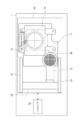
- FIG. 1 is a diagram schematically showing a failure analysis device 1 (semiconductor failure analysis device) according to the present embodiment.
- the failure analysis device 1 is a device that inspects the wafer W (analyzes the failure of the wafer W).
- Chips which are a plurality of semiconductor devices, are formed on the wafer W.
- Semiconductor devices include logic devices, memory devices, analog devices, mixed signal devices containing both digital and analog devices, discrete devices including power devices, photo devices including optical sensors and light emitting elements, passive elements including capacitors and coils, etc. There is.
- the failure analysis device 1 includes a failure analysis unit 10 (wafer transfer unit) and a controller 50.
- the controller 50 is a control unit that controls each configuration of the failure analysis unit 10 (details will be described later).
- the failure analysis unit 10 has a mounting table 11 (fixed portion), a platen 13, a test head 14, and a cable 15 as an observation position configuration for performing failure analysis of the wafer W. It has a probe card 16, a performance board 40, a connector board 41, and a pogo tower 42.
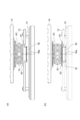
- FIG. 2 is a diagram for explaining the configuration of the wafer observation position.
- FIG. 2A shows a state in which the wafer W is not mounted on the mounting table 11, and
- FIG. 2B shows a state in which the wafer W is mounted on the mounting table 11.
- the mounting table 11 is a fixing portion for fixing the wafer at a predetermined observation position.
- the platen 13 is a flat plate-like member that holds the probe card 16. The platen 13 can be moved in the vertical direction by a Z stage (not shown) installed under the mounting table 11.
- the test head 14 is configured to apply a voltage to the needle 16a of the probe card 16 via the performance board 40, the cable 15, the connector board 41, and the pogo tower 42.
- the probe card 16 is a jig used for electrical inspection of the chip of the wafer W.
- the probe card 16 has a needle 16a protruding in the mounting table 11 direction.
- the needle 16a of the probe card 16 is formed on the chip on the surface of the wafer W by lowering the platen 13.
- the failure state of the chip is reproduced, and the failure analysis is performed on the chip to be inspected.
- FIG. 3 is a diagram illustrating backside observation of the wafer W.
- the tip of the solid immersion lens 80 is brought into close contact with the back surface Wb of the wafer W, and a high resolution image of the back surface Wb side of the wafer W is obtained. Is obtained.
- a plurality of wafer suction grooves 11a are formed on the mounting table 11. Since the wafer suction groove 11a is formed, the wafer W is appropriately fixed to the mounting table 11 by the vacuum chuck when the back surface Wb side is inspected in the failure reproduction state by applying the appropriate voltage described above. Will be done.
- the wafer W is moved by the wafer chuck 12, and failure analysis is performed on any chip of the wafer W.
- the fault analysis unit 10 has a wafer chuck 12, an X stage 21 and 21, and a Y stage 22 as a configuration for transporting while holding the wafer W. ..
- the X stages 21 and 21 are stages for moving the wafer chuck 12 holding the wafer W in the X direction (first direction).
- the Y stage 22 is a stage for moving the wafer chuck 12 holding the wafer W in the Y direction.
- the X direction and the Y direction are directions along the mounting surface of the wafer W on the wafer chuck 12 and intersect with each other. As shown in FIG.
- the wafer chuck 12 moves in the X direction along the X stages 21 and 21, so that the distance between the wafer chuck 12 and the mounting table 11 of the failure analysis unit 10 is increased.
- the X stages 21 and 21 extend in the X direction so as to face each other.
- the Y stage 22 is erected between the X stages 21 and 21, and is provided so as to be movable in the X direction along the X stages 21 and 21.
- the wafer chuck 12 is provided so as to be movable in the Y direction along the Y stage 22. According to such a configuration, the wafer chuck 12 moves in the X direction as the Y stage 22 moves along the X stages 21 and 21.
- the wafer chuck 12 is a transport unit that transports the wafer W to the mounting table 11, which is the observation position, while holding the wafer W. As described above, the wafer chuck 12 is movable in the X direction and the Y direction (direction along the mounting surface of the wafer W in the wafer chuck 12) by the X stages 21 and 21 and the Y stage 22. The wafer chuck 12 sequentially transfers a plurality of wafers W, which are automatically exchanged by, for example, a wafer transfer robot 60 (see FIG. 4), to the mounting table 11.
- FIG. 4 is a diagram illustrating wafer replacement by the wafer transfer robot 60.
- FIG. 4 shows a wafer transfer robot 60 and a wafer cassette 70 as configurations related to wafer exchange.
- a plurality of wafers W to be analyzed for failure are divided by partitions in the wafer cassette 70, and are stacked in a state of being placed on each partition.
- the wafer transfer robot 60 lifts one wafer W from the wafer cassette 70 from the back surface by the hand 61, sucks it, moves it, and delivers it to the wafer chuck 12.
- the wafer transfer robot 60 may deliver the wafer W to the wafer chuck 12 via the wafer holder 19 and the wafer base 51 (see FIG. 9) described later.
- the wafer chuck 12 conveys the wafer W to the mounting table 11 while holding the wafer W by a holding member described later, and when the failure analysis of the wafer W is completed on the mounting table 11, the wafer W is transferred to the vicinity of the wafer transfer robot 60. Transport. Then, the wafer transfer robot 60 takes out the wafer W for which the failure analysis has been completed from the wafer chuck 12, holds and conveys the next wafer W stacked on the wafer cassette 70, and places it on the mounting surface of the wafer chuck 12. do. The above is the wafer exchange by the wafer transfer robot 60.
- a wafer base 51 and a wafer holder 19 are provided in the vicinity of the wafer exchange portion where the wafer transfer robot 60 and the wafer cassette 70 are provided.
- the wafer base 51 is a mounting table on which the wafer W is placed when the wafer is replaced.
- the wafer base 51 may be set at the same height as the mounting table 11 so that the wafer W can be slid and moved. Further, the configuration does not include the wafer base 51 and the wafer holder 19, but may be a configuration in which the wafer holder 19 is simply arranged in the mounting table 11.
- the wafer holder 19 is configured to be able to move up and down, and by pushing up the wafer W placed on the wafer base 51 from the back surface side, the wafer W is delivered to and from the wafer transfer robot 60 (details will be described later). ).
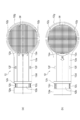
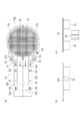
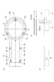
- FIG. 5 is a diagram illustrating a wafer holding state (FIG. 5A) and a wafer opening state (FIG. 5B) by the wafer chuck 12.
- the wafer chuck 12 has a plurality of holding members provided so as to face the side surface of the wafer W.
- the plurality of holding members are configured to include four protrusions 12x, 12x, 12y, 12y.
- the protruding portions 12x, 12x, 12y, and 12y are configured to sandwich the wafer W.
- the plurality of holding members include a first holding member including two protrusions 12y and 12y that abut on the peripheral portion of the wafer W, and a second holding member including two protrusions 12x and 12x. Have.
- the wafer chuck 12 includes a base portion 12a, a core portion 12b, an elastic member 12c, and a ring portion 12d.
- the base portion 12a is a portion connected to the Y stage 22.
- the ring portion 12d is a pair of a first portion 12k connected to the base portion 12a via a pair of elastic members 12c and 12c and a pair extending in the X direction (first direction) while being continuous with the first portion 12k and facing each other.
- the pair of second portions 12e and 12e are formed with hole portions 12f and 12f configured to be engageable with the ratchet mechanism 18 (stopping portion; see FIG. 9).
- the ratchet mechanisms 18 and 18 engage with the holes 12f and 12f to fix the positions of the second portions 12e and 12e in which the holes 12f and 12f are formed.
- the ratchet mechanism 18 fixes the positions of the protrusions 12y and 12y, which are the first holding members, by fixing the positions of the second portions 12e and 12e, and between the protrusions 12y and 12y and the protrusions 12x and 12x.
- the separation distance is changed so that the sandwiched state of the wafer W by the protrusions 12y and 12y and the protrusions 12x and 12x can be released (details will be described later). That is, in a state where the position of the ring portion 12d (that is, the positions of the protruding portions 12y and 12y) is fixed by engaging the ratchet mechanism 18 with the second portion 12e, only the core portion 12b is as shown in FIG.
- the distance between the protrusions 12y and 12y and the protrusions 12x and 12x is increased, the protrusions 12x and 12x do not come into contact with the wafer W, and the wafer W The pinched state is released.
- the elastic member 12c may be an elastic spring member or a rubber (such as a rubber band made of silicon rubber).
- the core portion 12b is continuous with the base portion 12a and extends in the X direction (first direction) between the pair of second portions 12e and 12e. At the tip of the core portion 12b (the end opposite to the side continuous with the base portion 12a in the X direction), there is a second holding member protruding toward the accommodation space in which the wafer W is placed (accommodated). Protruding portions 12x and 12x are provided.
- the third portion 12g of the ring portion 12d is provided with projecting portions 12y and 12y which are first holding members projecting toward the accommodation space having a substantially circular shape in a plan view for accommodating (mounting) the wafer W.
- projecting portions 12y and 12y which are first holding members projecting toward the accommodation space having a substantially circular shape in a plan view for accommodating (mounting) the wafer W.
- the direction of the force applied to the wafer W by the protruding portions 12x and 12x which are the second holding members for sandwiching the wafer W, and the first holding member for sandwiching the wafer W.
- the directions of the forces exerted by the protruding portions 12y and 12y on the wafer W are opposite to each other in the X direction.
- the positions where the protrusions 12x, 12x, 12y and 12y are provided are not particularly limited, but for example, the positions where the protrusions 12y and 12y are provided are provided with the protrusions 12x and 12x in the Y direction. It is outside the position where it is.
- the wafer chuck 12 is formed by the protrusions 12x, 12x, which are the second holding members, and the protrusions 12y, 12y, which are the first holding members.
- the wafer W is held by sandwiching the peripheral portion of the wafer W.
- the wafer chuck 12 in the wafer open state, has the protrusions 12x and 12x which are the second holding members and the protrusions 12y and 12y which are the first holding members. It is not in contact with the wafer W and does not sandwich the wafer W.
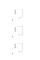
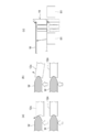
- FIG. 6 is a diagram schematically showing an example of the shape of the protruding portion 12x (and the protruding portion 12y) which is the holding member.
- the protruding portion 12x shown in FIGS. 6 (a) and 6 (b) both has a shape that sandwiches the wafer W to be sandwiched, and has a shape that is recessed toward the center.
- the surface of the portion sandwiching the wafer W is a curved surface.
- the protruding portion 12x shown in FIG. 6B the surface of the portion sandwiching the wafer W is not curved, and the central portion is formed in a concave valley shape.
- the protruding portion 12x shown in FIG. 6C has a shape that pushes the wafer W downward.
- FIG. 7 schematically illustrates an example of a contact structure between the wafer W and the protrusion 12x (FIGS. 7 (a) and 7 (b)) and an example of a contact structure between the wafer W and the wafer holder 19 (FIG. 7 (c)). It is a figure which shows. As will be described later, when the wafer W is taken out from the wafer chuck 12, the wafer W is lifted by the wafer holder 19 from below. In this case, as shown in FIG. 7A, the wafer W may slide and rise on the slope of the protruding portion 12x of the wafer chuck 12. Even when it is difficult to slide and rise in this way, as shown in FIG.
- the protruding portion 12x of the wafer chuck 12 is distorted as the wafer W rises (wafer W is distorted).
- the wafer W can be appropriately taken out from the wafer chuck 12 by distorting in the direction in which it tends to rise).
- the protrusion 12x is made of a material having a certain degree of plasticity.
- the wafer W may be provided with a slope and the wafer W may be slid to positively shift the wafer W to facilitate the removal of the wafer W.
- the controller 50 is a computer, and is physically configured to include a memory such as a RAM and a ROM, a processor (arithmetic circuit) such as a CPU, a communication interface, and a storage unit such as a hard disk. ..
- Examples of the controller 50 include personal computers, cloud servers, smart devices (smartphones, tablet terminals, etc.) and the like.
- the controller 50 functions by executing a program stored in the memory on the CPU of the computer system.
- the controller 50 controls the X stage 21, the Y stage 22, the Z stage (not shown), and the like. By controlling the X stage 21 and the Y stage 22, the controller 50 switches between the wafer holding state and the wafer opening state, and conveys the wafer W.
- FIGS. 8 to 16 show a continuous process.
- 8 to 11 show, for example, a step of transporting the wafer W after failure analysis to a wafer exchange location (near the wafer transfer robot 60), and
- FIG. 12 shows a wafer exchange process by the wafer transfer robot 60.
- 13 to 16 show a process of transporting the new wafer W to the mounting table 11.
- (a) to (c) (or (a) to (b)) having the same drawing numbers indicate states of the same timing.
- the X direction is the right direction in the figure (the direction from the mounting table 11 to the wafer base 51), and the ⁇ X direction is the left direction in the figure (the direction opposite to the direction from the mounting table 11 to the wafer base 51). ) Will be described as showing each.
- the wafer chuck 12 holding the wafer W is now moving in the ⁇ X direction under the control of the X stage 21 by the controller 50.
- the positions of Y of the ratchet mechanisms 18 and 18 provided in the vicinity of the wafer exchange points and the positions of Y of the holes 12f and 12f of the wafer chuck 12 are determined by controlling the Y stage 22 by the controller 50. Match.
- the X positions of the holes 12f and 12f of the wafer chuck 12 have not reached the X positions of the ratchet mechanisms 18 and 18.
- FIG. 8A the X positions of the holes 12f and 12f of the wafer chuck 12 have not reached the X positions of the ratchet mechanisms 18 and 18.
- the wafer W is placed on the wafer base 51 so that the center of the wafer base 51 and the center of the wafer W coincide with each other as shown in FIG. 9A.
- the ratchet mechanisms 18 and 18 and the holes 12f and 12f of the wafer chuck 12 are engaged with each other (see FIG. 9B).
- the ratchet mechanism 18 impedes the movement (movement) of the ring portion 12d in the ⁇ X direction by passing through the hole portion 12f by the spring mechanism and projecting upward.
- the position of the ring portion 12d is fixed, and the position of the configuration (including the protruding portions 12y and 12y) related to the ring portion 12d does not change.
- the wafer chuck 12 moves in the same direction, only the base portion 12a and the core portion 12b move in the same direction, and the position of the ring portion 12d does not change.
- Such a difference in position between the base portion 12a and the core portion 12b and the ring portion 12d is absorbed by the expansion and contraction of the elastic member 12c.
- the core portion 12b moves to a position where a space larger than the overhang inner diameters of the protruding portions 12x and 12x is opened and stops.
- the wafer holder 19 rises and pushes up the wafer W from the back surface side under the control of the controller 50.
- the wafer W slides on the slope of the wafer holder 19, and the wafer W can be placed at a position where the center of the wafer holder 19 and the center of the wafer W coincide with each other.
- the wafer transfer robot 60 is controlled by the controller 50 in a state where the wafer holder 19 is raised, so that the wafer W1 which is the wafer W after the failure analysis is unloaded ( Removal) is carried out, and then the wafer W2, which is the wafer W before the failure analysis, is loaded.
- the notch sensor 43 specifies the location of the notch of the wafer W2, the inclination of the wafer W2 is adjusted, and the wafer W2 is set at the correct angle.
- FIG. 12A shows a wafer chuck 12, a wafer base 51, and a wafer holder 19 in a state where the wafer W (wafer W1) is unloaded.
- the wafer holder 19 is lowered and the wafer W is placed on the wafer base 51 under the control of the controller 50.
- the wafer holder 19 retracts below the wafer base 51.
- the base portion 12a and the core portion 12b move in the X direction by the control of the X stage 21 by the controller 50, and the protruding portions 12x and 12x move to the peripheral portion of the wafer W.
- the ring portion 12d is restricted from moving in the X direction by engaging the ratchet mechanisms 18 and 18 with the holes 12f and 12f of the wafer chuck 12 (see FIG. 14B). There is.
- the base portion 12a and the core portion 12b are further moved in the X direction by the control of the X stage 21 by the controller 50, and the protruding portions 12x and 12x move the wafer W in the X direction.
- the peripheral portion of the wafer W comes into contact with the protruding portions 12y and 12y of the ring portion 12d.
- a force is applied to the wafer W from both sides by the protruding portions 12x, 12x and the protruding portions 12y, 12y to sandwich the wafer W, so that the wafer W being conveyed is fixed.
- a force in the X direction starts to be applied to the ring portion 12d, and as shown in FIG. 15B, the engagement state between the ratchet mechanisms 18 and 18 and the hole portions 12f and 12f of the wafer chuck 12 is changed. It will be released. That is, the ring portion 12d is released from the ratchet mechanism 18.
- the wafer chuck 12 is X by the control of the X stage 21 by the controller 50 in a state where the peripheral portion of the wafer W is sandwiched by the protruding portions 12x, 12x, 12y, 12y. Move in the direction. That is, the wafer chuck 12 is separated from the wafer base 51 and moves toward the mounting table 11. The wafer W can be sandwiched and sandwiched from the left and right (both sides) by the elastic member 12c provided at the base of the wafer chuck 12.
- a configuration including a wafer chuck 12 on which a wafer W is placed and transferred is known.
- a method of firmly holding the wafer W on the wafer chuck 12 as shown in FIG. 17A, there is a method of fixing the surface side of the wafer W to the wafer chuck 12 with tape 300.
- the height of the tape 300 is low. Therefore, when the needle 16a of the probe card 16 is touched down from the surface side of the wafer W to the pad of the wafer W, it is advantageous in that the chip near the wafer edge can be accessed.
- the wafer transfer robot 60 may move the wafer W from the wafer cassette 70 to the wafer chuck 12, and such a wafer transfer robot.
- the wafer transfer robot 60 may move the wafer W from the wafer cassette 70 to the wafer chuck 12, and such a wafer transfer robot.
- it is difficult to adopt the method of fixing the wafer W to the wafer chuck 12 with the tape 300. Therefore, there is a demand for a configuration in which the wafer W being conveyed is firmly held by a configuration other than fixing with the tape 300.
- the height of the fixture 200a is the height from the bottom surface of the probe card 16 to the tip of the needle 16a. It will be higher than that, and the touchdown described above may not be possible. Further, for example, as shown in FIG. 17 (c), when a fixture 200b having a relatively low height is used, touchdown is not impossible unlike the fixture 200a, but the probe is located near the wafer edge. Interference may occur depending on the design of the card 16.
- the holding means is used. There are restrictions on the position, thickness, etc., and no suitable holding means has been found.
- the failure analysis unit 10 is a wafer transfer unit that transfers the wafer W while holding it in the semiconductor failure analysis device, and fixes the wafer W at a predetermined observation position.
- a mounting table 11 and a wafer chuck 12 for transporting the wafer W to the observation position while holding the wafer W are provided, and the wafer chuck 12 is provided with a plurality of holding members (projecting portions 12x, It has 12x, 12y, 12y), and holds the wafer W by sandwiching the peripheral portion of the wafer W with a plurality of holding members.
- the wafer W is conveyed by the wafer chuck 12 to the observation position where the wafer W is fixed. Then, the wafer chuck 12 sandwiches the peripheral portion of the wafer W by a plurality of protruding portions 12x, 12x, 12y, 12y provided so as to face the side surface of the wafer W. In this way, by adopting a configuration in which the protruding portions 12x, 12x, 12y, 12y of the wafer chuck 12 sandwich the peripheral portion of the wafer W from the side surface of the wafer W, the wafer W being conveyed can be firmly held. It is not necessary to provide a new configuration on the back surface side and the front surface side of the wafer W. As a result, the wafer W being conveyed can be appropriately held without interfering with each function of the semiconductor failure analysis apparatus.
- the plurality of holding members may be configured to include at least four protrusions 12x, 12x, 12y, 12y. Thereby, the wafer W can be sandwiched more stably.
- the plurality of holding members include a first holding member including a plurality of protruding portions 12y and 12y that abut on the peripheral portion of the wafer W, and a second holding member including a plurality of protruding portions 12x and 12x.
- the direction of the force applied to the wafer W by the first holding member holding the W may be opposite to the direction of the force applied to the wafer W by the second holding member holding the wafer W.
- the failure analysis unit 10 changes the separation distance between the first holding member and the second holding member by fixing the position of only the first holding member, and the first holding member and the second holding member.
- a ratchet mechanism 18 configured to be able to release the sandwiched state of the wafer W by the holding member may be further provided. According to such a configuration, the sandwiched state of the wafer W can be appropriately released (the wafer W is opened) by a simple configuration in which the position of only the first holding member is fixed.
- the wafer chuck 12 includes a base portion 12a, a first portion 12k connected to the base portion 12a via an elastic member 12c, and a pair of second portions extending in the X direction while being continuous with the first portion 12k and facing each other.
- a ring portion 12d including 12e, 12e, a third portion 12g continuous with the tip of the pair of second portions 12e and formed in a ring shape so as to partition a storage space for accommodating the wafer, and a base portion 12a.
- the third portion 12g of the ring portion 12d has a core portion 12b which is continuous with the second portion 12e and extends in the X direction between the pair of second portions 12e and 12e, and the protruding portions 12y and 12y projecting toward the accommodation space.
- the wafer W is appropriately sandwiched by the protrusions 12y and 12y and the protrusions 12x and 12x that protrude toward the accommodation space.
- the protruding portions 12y and 12y provided on the ring portion 12d and the protruding portions 12x provided on the core portion 12b The separation distance from the 12x becomes large, and the sandwiched state of the wafer W by the protruding portions 12y and 12y and the protruding portions 12x and 12x is released.
- the wafer W can be easily sandwiched and released (opened) by the above-described configuration.
- the chuck / unchuck of the wafer is realized by the operation of the X stage, and it is not necessary to provide another chuck / unchuck drive mechanism. As a result, the reliability of the wafer load / unload system can be improved.
- the present invention is not limited to the above embodiments.
- at least four protrusions are provided as the holding member, but as shown in FIG. 18, there may be three protrusions. That is, in the wafer chucks shown in FIGS. 18A and 18B, two protrusions 512x and 512x are provided at the tip of the core portion 512b, and the third portion 512g of the ring portion 512d is provided.
- One protrusion 512y is provided.
- the position where the protrusions 512x, 512x, 512y are provided is not particularly limited, but for example, the position where the protrusions 512x, 512x are provided is higher than the position where the protrusions 512y are provided in the Y direction. It is the outside.
- 10 Failure analysis unit (wafer transfer unit), 11 ... mounting base (fixed part), 12 ... wafer chuck (conveyed part), 12a ... base part, 12b ... core part, 12c ... elastic member, 12d ... ring part, 12e ... 2nd part, 12f ... hole, 12g ... 3rd part, 12k ... 1st part, 12x, 12x, 12y, 12y ... protruding part, 18 ... ratchet mechanism (stopping part), 19 ... wafer holder, 21 ... X stage , 22 ... Y stage, 40 ... Performance board, 41 ... Connector board, 42 ... Pogo tower, 43 ... Notch sensor, 50 ... Controller, 51 ...
- Wafer base 60 ... Wafer transfer robot, 61 ... Hand, 70 ... Wafer cassette, 80 ... Solid immersion lens, 200a, 200b ... Fixture, 300 ... Tape, 512b ... Core part, 512d ... Ring part, 512x ... Protruding part, 512y ... Protruding part, W ... Wafer.
Landscapes
- Engineering & Computer Science (AREA)
- General Engineering & Computer Science (AREA)
- Physics & Mathematics (AREA)
- General Physics & Mathematics (AREA)
- Environmental & Geological Engineering (AREA)
- Computer Hardware Design (AREA)
- Microelectronics & Electronic Packaging (AREA)
- Container, Conveyance, Adherence, Positioning, Of Wafer (AREA)
- Testing Or Measuring Of Semiconductors Or The Like (AREA)
- Manufacturing & Machinery (AREA)
- Robotics (AREA)
- Die Bonding (AREA)
Abstract
故障解析ユニットは、半導体故障解析装置においてウェハを保持しながら搬送するウェハ搬送ユニットであって、所定の観察位置にウェハを固定する載置台と、観察位置までウェハを保持しながら搬送するウェハチャックと、を備え、ウェハチャックは、ウェハの側面と対向するように設けられた複数の保持部材(突出部)を有し、複数の保持部材によってウェハWの周部を挟持することによりウェハを保持する。
Description
本発明の一態様は、半導体故障解析装置においてウェハを保持しながら搬送するウェハ搬送ユニット及びウェハ搬送方法に関する。
半導体故障解析装置において、ウェハを保持しながら搬送する機構(ウェハ搬送機構)が知られている(例えば特許文献1参照)。
上述したようなウェハ搬送機構として、ウェハを載置して搬送するウェハチャックを含む構成が知られている。従来、ウェハチャックにウェハを強固に保持する方法として、テープでウェハチャックにウェハを固定する方法がある。近年、複数枚のウェハに対して自動で故障解析を実行すべく、ウェハ搬送ロボットによってウェハカセットからウェハチャックにウェハを移動させる場合があるところ、このようなウェハ搬送ロボットを用いる場合には、ウェハチャックにウェハをテープで固定する方法は採用し難い。そこで、テープで固定する以外の方法で搬送中のウェハを強固に保持することが求められている。
また、上述したような半導体故障解析装置においては、ウェハチャック等によりウェハが保持された状態において、ウェハの裏面側から、先端に半球状の部材を装着した固浸レンズと呼ばれる特殊なレンズを密着させて高分解能の画像を取得する場合がある。固浸レンズを密着させてウェハ内の任意のチップを解析するためには、ウェハ裏面の全体が露出している必要がある。このため、ウェハの裏面側から固浸レンズを密着させる構成においては、搬送中のウェハを強固に保持するための構成をウェハの裏面側以外に設ける必要がある。
さらに、上述したような半導体故障解析装置においては、ウェハの表面側からプローブカードの針をウェハのパッドにタッチダウンしてウェハにバイアスを印加するところ、ウェハの表面側に搬送中のウェハを強固に保持する固定具が設けられた場合には固定具がプローブカードの針のタッチダウン処理を妨げたり、プローブカードの針を破損させたりする可能性がある。以上のように、ウェハ搬送機構においては、テープ以外の方法で搬送中のウェハを強固に保持することが求められているものの、半導体故障解析装置の各機能を実現する上で、保持手段の位置及び厚み等に制限があり、適切な保持手段が見出されていない。
本発明の一態様は上記実情に鑑みてなされたものであり、半導体故障解析装置の各機能を妨げることなく、搬送中のウェハを適切に保持することができる、ウェハ搬送ユニット及びウェハ搬送方法を提供することを目的とする。
本発明の一態様に係るウェハ搬送ユニットは、半導体故障解析装置においてウェハを保持しながら搬送するウェハ搬送ユニットであって、所定の観察位置にウェハを固定する固定部と、観察位置までウェハを保持しながら搬送する搬送部と、を備え、搬送部は、ウェハの側面と対向するように設けられた複数の保持部材を有し、複数の保持部材によってウェハの周部を挟持することによりウェハを保持する。
本発明の一態様に係るウェハ搬送ユニットでは、ウェハが固定される観察位置まで、搬送部によってウェハが搬送される。そして、搬送部は、ウェハの側面と対向するように設けられた複数の保持部材によってウェハの周部を挟持する。このように、搬送部の保持部材がウェハの側面からウェハの周部を挟持する構成を採用することによって、搬送中のウェハを強固に保持するための新たな構成をウェハの裏面側及び表面側に設ける必要がない。このことにより、半導体故障解析装置の各機能を妨げることなく、搬送中のウェハを適切に保持することができる。
複数の保持部材は、ウェハの周部に当接する少なくとも3つの突出部を含んで構成されていてもよい。これにより、ウェハを安定的に挟持することができる。
複数の保持部材は、少なくとも4つの突出部を含んで構成されていてもよい。これにより、ウェハをより安定的に挟持することができる。
複数の保持部材は、ウェハの周部に当接する一又は複数の突出部を含む第1の保持部材と、一又は複数の突出部を含む第2の保持部材とを有し、ウェハを挟持する第1の保持部材がウェハに与える力の方向と、ウェハを挟持する第2の保持部材がウェハに与える力の方向とは互いに反対の方向であってもよい。第1の保持部材がウェハに与える力の方向と第2の保持部材がウェハに与える力の方向とを互いに反対の方向とすることにより、第1の保持部材及び第2の保持部材によってウェハを適切に挟持することができる。
上記のウェハ搬送ユニットは、第1の保持部材及び第2の保持部材のいずれか一方のみの位置を固定することにより、第1の保持部材及び第2の保持部材間の離間距離を変化させ、第1の保持部材及び第2の保持部材によるウェハの挟持状態を解除可能に構成された歯止め部を更に備えていてもよい。このような構成によれば、第1の保持部材及び第2の保持部材のいずれか一方のみの位置を固定するという簡易な構成によって、ウェハの挟持状態を適切に解除する(ウェハを開放する)ことができる。
搬送部は、ベース部と、弾性部材を介してベース部に接続された第1部分と、第1部分に連続すると共に互いに対向しながら第1方向に延びる一対の第2部分と、一対の第2部分の先端に連続すると共にウェハを収容する収容スペースを区画するようにリング状に形成された第3部分と、を含むリング部と、ベース部に連続すると共に一対の第2部分間において第1方向に延びるコア部と、を有し、リング部の第3部分には、収容スペースに向かって突出した第1の保持部材が設けられており、コア部の先端には、収容スペースに向かって突出した第2の保持部材が設けられており、リング部の一対の第2部分には、歯止め部と係合可能に構成された孔部が形成されており、歯止め部は、孔部と係合することにより、リング部の位置を固定して第1の保持部材の位置を固定してもよい。このような構成によれば、収容スペースに向かって突出した第1の保持部材と第2の保持部材とによって、ウェハが適切に挟持される。そして、リング部の一対の第2部分の孔部が歯止め部と係合することにより、リング部が固定され第1の保持部材の位置が固定される。このような場合において、リング部とベース部とは弾性部材を介して接続されていることから、弾性部材が延びることによって、リング部の位置が固定された状態においてもベース部及びベース部に連続するコア部は変位可能となる。リング部の位置が固定された状態でコア部が収容スペースから離れる方向に変位することにより、リング部に設けられた第1の保持部材とコア部に設けられた第2の保持部材との離間距離が大きくなり、第1の保持部材及び第2の保持部材によるウェハの挟持状態が解除されることになる。以上のように、上述した構成によって、ウェハの適切な挟持及び解除(開放)を容易に行うことができる。
本発明の一態様に係るウェハ搬送方法は、半導体故障解析装置においてウェハを保持しながら搬送するウェハ搬送方法であって、ウェハの側面と対向するように設けられた複数の保持部材によってウェハの周部を挟持する工程と、複数の保持部材によってウェハの周部を挟持した状態で、ウェハを所定の観察位置まで搬送する工程と、を含む。
本発明の一態様によれば、半導体故障解析装置の各機能を妨げることなく、搬送中のウェハを適切に保持することができる。
以下、本発明の実施形態について、図面を参照して詳細に説明する。なお、各図において同一又は相当部分には同一符号を付し、重複する説明を省略する。
図1は、本実施形態に係る故障解析装置1(半導体故障解析装置)を模式的に示す図である。故障解析装置1は、ウェハWを検査する(ウェハWの故障を解析する)装置である。ウェハW上には複数の半導体デバイスであるチップが形成されている。半導体デバイスとしては、ロジックデバイス、メモリデバイス、アナログデバイス、デジタルとアナログを混載したミックスドシグナルデバイス、パワーデバイスを含むディスクリートデバイス、光センサや発光素子を含むフォトデバイス、コンデンサやコイルを含む受動素子等がある。
図1に示されるように、故障解析装置1は、故障解析ユニット10(ウェハ搬送ユニット)と、コントローラ50とを備えている。コントローラ50は、故障解析ユニット10の各構成を制御する制御部である(詳細は後述)。故障解析ユニット10は、図1及び図2に示されるように、ウェハWの故障解析を行う観察位置の構成として、載置台11(固定部)と、プラテン13と、テストヘッド14と、ケーブル15と、プローブカード16と、パフォーマンスボード40と、コネクタボード41と、ポゴタワー42と、を有している。
図2は、ウェハ観察位置の構成を説明する図である。図2(a)は載置台11にウェハWが載置されていない状態を示しており、図2(b)は載置台11にウェハWが載置されている状態を示している。載置台11は、所定の観察位置にウェハを固定する固定部である。プラテン13は、プローブカード16を保持する平板状部材である。プラテン13は、載置台11の下部に設置されたZステージ(不図示)によって上下方向に移動可能とされている。テストヘッド14は、パフォーマンスボード40、ケーブル15、コネクタボード41、ポゴタワー42を介してプローブカード16の針16aに電圧を印加する構成である。プローブカード16は、ウェハWのチップの電気的検査に用いられる治具である。プローブカード16は、載置台11方向に突出した針16aを有している。図2(b)に示されるように、載置台11にウェハWが固定された状態において、プラテン13が下降することによりプローブカード16の針16aがウェハWの表面のチップ上に形成されたパッドにタッチダウンし、テストヘッド14によって適切な電圧が印可されることにより、チップの故障状態が再現され、検査対象のチップについて故障解析が実施される。
図3は、ウェハWの裏面観察について説明する図である。ウェハ観察位置におけるウェハWの故障解析においては、図3(a)に示されるように、ウェハWの裏面Wbに固浸レンズ80の先端を密着させて、ウェハWの裏面Wb側の高分解能画像が取得される。載置台11には、複数のウェハ吸着溝11aが形成されている。ウェハ吸着溝11aが形成されていることによって、上述した適切な電圧印加による故障再現状態における裏面Wb側の検査を実施している際には、真空チャックによりウェハWが載置台11に適切に固定される。図3(b)に示されるように、ウェハチャック12によってウェハWが移動させられ、ウェハWの任意のチップについて故障解析が行われる。
図1に戻り、故障解析ユニット10は、ウェハWを保持しながら搬送するための構成として、ウェハチャック12(搬送部)と、Xステージ21,21と、Yステージ22と、を有している。Xステージ21,21は、ウェハWを保持しているウェハチャック12をX方向(第1方向)に移動させるステージである。Yステージ22は、ウェハWを保持しているウェハチャック12をY方向に移動させるステージである。X方向及びY方向とは、ウェハチャック12におけるウェハWの載置面に沿った方向であり、互いに交差する方向である。図1に示されるように、本実施形態では、ウェハチャック12がXステージ21,21に沿ってX方向に移動することにより、ウェハチャック12と故障解析ユニット10の載置台11との離間距離が変化する。Xステージ21,21は、互いに対向するようにX方向に延びている。Yステージ22は、Xステージ21,21間に架設されており、Xステージ21,21に沿ってX方向に移動可能に設けられている。ウェハチャック12は、Yステージ22に沿ってY方向に移動可能に設けられている。このような構成によれば、Yステージ22がXステージ21,21に沿って移動することによりウェハチャック12がX方向に移動する。
ウェハチャック12は、観察位置である載置台11までウェハWを保持しながら搬送する搬送部である。上述したように、ウェハチャック12は、Xステージ21,21及びYステージ22によって、X方向及びY方向(ウェハチャック12におけるウェハWの載置面に沿った方向)に移動可能とされている。ウェハチャック12は、例えばウェハ搬送ロボット60(図4参照)によって自動で交換される複数枚のウェハWを、順次、載置台11まで搬送する。
図4は、ウェハ搬送ロボット60によるウェハ交換を説明する図である。図4には、ウェハ交換に係る構成として、ウェハ搬送ロボット60と、ウェハカセット70とが図示されている。図4に示されるように、ウェハカセット70には、故障解析対象の複数のウェハWが仕切りで分けられ、各仕切り上に載置された状態で積層されている。ウェハ搬送ロボット60は、ハンド61によってウェハカセット70からウェハWの1枚を裏面から持ち上げて吸着して移動し、ウェハチャック12に受け渡す。この際、ウェハ搬送ロボット60は、後述するウェハホルダ19及びウェハベース51(図9参照)を介して、ウェハチャック12にウェハWを受け渡してもよい。ウェハチャック12は、後述する保持部材によってウェハWを保持しながら載置台11までウェハWを搬送し、載置台11においてウェハWの故障解析が終了すると、該ウェハWをウェハ搬送ロボット60の近傍まで搬送する。そして、ウェハ搬送ロボット60は、故障解析が終了したウェハWをウェハチャック12から取り出し、ウェハカセット70に積層されている次のウェハWを保持・搬送してウェハチャック12の載置面に載置する。以上がウェハ搬送ロボット60によるウェハ交換である。
ウェハ搬送ロボット60及びウェハカセット70が設けられたウェハ交換箇所の近傍には、図8及び図9等に示されるように、ウェハベース51及びウェハホルダ19が設けられている。ウェハベース51は、ウェハ交換時にウェハWを載置する載置台である。ウェハベース51は、ウェハWをスライドさせて移動させるべく、載置台11と同じ高さに設定されていてもよい。また、ウェハベース51及びウェハホルダ19を含んだ構成ではなく、単に載置台11中にウェハホルダ19が配置された構成であってもよい。ウェハホルダ19は、上下に昇降可能に構成されており、ウェハベース51に載置されたウェハWを裏面側から押し上げることにより、ウェハ搬送ロボット60との間でウェハWの受け渡しを行う(詳細は後述)。
ウェハチャック12によるウェハWの保持に係る構成について、図5を参照して説明する。図5は、ウェハチャック12によるウェハ保持状態(図5(a))及びウェハ開放状態(図5(b))を説明する図である。ウェハチャック12は、ウェハWの側面と対向するように設けられた複数の保持部材を有している。当該複数の保持部材は、4つの突出部12x,12x,12y,12yを含んで構成されている。突出部12x,12x,12y,12yは、ウェハWを挟持する構成である。詳細には、複数の保持部材は、ウェハWの周部に当接する2つの突出部12y,12yを含む第1の保持部材と、2つの突出部12x,12xを含む第2の保持部材とを有している。
ウェハチャック12は、ベース部12aと、コア部12bと、弾性部材12cと、リング部12dと、を含んで構成されている。ベース部12aは、Yステージ22に接続される部分である。リング部12dは、一対の弾性部材12c,12cを介してベース部12aに接続される第1部分12kと、第1部分12kに連続すると共に互いに対向しながらX方向(第1方向)に延びる一対の第2部分12e,12eと、一対の第2部分12eの先端(X方向における第1部分12kに連続する側と反対側の端部)に連続すると共にウェハWを収容(載置)する平面視略円形の収容スペースを区画するようにリング状に形成された第3部分12gと、を含んでいる。
一対の第2部分12e,12eには、ラチェット機構18(歯止め部。図9参照)と係合可能に構成された孔部12f,12fが形成されている。ラチェット機構18,18は、孔部12f,12fと係合することにより、孔部12f,12fが形成された第2部分12e,12eの位置を固定する。ラチェット機構18は、第2部分12e,12eの位置を固定することにより、第1の保持部材である突出部12y,12yの位置を固定し、突出部12y,12y及び突出部12x,12x間の離間距離を変化させ、突出部12y,12y及び突出部12x,12xによるウェハWの挟持状態を解除可能に構成されている(詳細は後述)。すなわち、ラチェット機構18が第2部分12eと係合することによりリング部12dの位置(すなわち突出部12y,12yの位置)が固定された状態で、図10に示されるようにコア部12bのみがX方向(且つウェハWから離間する方向)に移動することによって、突出部12y,12y及び突出部12x,12x間の距離が開き、突出部12x,12xがウェハWに接触しなくなり、ウェハWの挟持状態が解除される。
弾性部材12cは、弾性を有するばね部材であってもよいし、ゴム(シリコンゴムの輪ゴム等)であってもよい。コア部12bは、ベース部12aに連続すると共に、一対の第2部分12e,12e間においてX方向(第1方向)に延びている。コア部12bの先端(X方向におけるベース部12aに連続する側と反対側の端部)には、ウェハWが載置(収容)される収容スペースに向かって突出した第2の保持部材である突出部12x,12xが設けられている。また、リング部12dの第3部分12gには、ウェハWを収容(載置)する平面視略円形の収容スペースに向かって突出した第1の保持部材である突出部12y,12yが設けられている。図5(a)に示されるように、ウェハWを挟持する第2の保持部材である突出部12x,12xがウェハWに与える力の方向と、ウェハWを挟持する第1の保持部材である突出部12y,12yがウェハWに与える力の方向とは、X方向において互いに反対の方向である。突出部12x,12x,12y,12yが設けられている位置については特に限られないが、例えば突出部12y,12yが設けられている位置は、Y方向において、突出部12x,12xが設けられている位置よりも外側である。
図5(a)に示されるように、ウェハ保持状態においては、ウェハチャック12は、第2の保持部材である突出部12x,12x及び第1の保持部材である突出部12y,12yによってウェハWの周部を挟持することにより、ウェハWを保持する。また、図5(b)に示されるように、ウェハ開放状態においては、ウェハチャック12は、第2の保持部材である突出部12x,12x及び第1の保持部材である突出部12y,12yがウェハWに接触しておらず、ウェハWを挟持していない。
突出部12x(及び突出部12y)の詳細な構成について、図6及び図7を参照して説明する。図6は、保持部材である突出部12x(及び突出部12y)の形状の一例を模式的に示す図である。図6(a)及び図6(b)に示される突出部12xは、いずれも挟持するウェハWを挟み込む形状であり、中央部ほど凹んだ形状とされている。図6(a)に示される突出部12xは、ウェハWを挟み込む部分の面が曲面になっている。一方で、図6(b)に示される突出部12xは、ウェハWを挟み込む部分の面が曲面になっておらず、中央部が凹んだ谷状に形成されている。図6(c)に示される突出部12xは、ウェハWを下方へ押し付ける形状である。
図7は、ウェハWと突出部12xとの接触構造の一例(図7(a)及び図7(b))並びにウェハWとウェハホルダ19との接触構造の一例(図7(c))を模式的に示す図である。後述するように、ウェハチャック12からウェハWを取り出す際には、下からウェハホルダ19によってウェハWが持ち上げられる。この場合、図7(a)に示されるように、ウェハチャック12の突出部12xの斜面をウェハWが滑って上昇してもよい。このように滑って上昇することが困難である場合であっても、例えば図7(b)に示されるように、ウェハWの上昇に伴ってウェハチャック12の突出部12xが歪む(ウェハWが上昇しやすくなる方向に歪む)ことにより、ウェハチャック12からウェハWを適切に取り出すことができる。この場合、突出部12xは一定の可塑性を有する材質で構成される。なお、図7(c)に示されるように、ウェハホルダ19に斜面を設け、ウェハWを滑らせることによって積極的にウェハWをずらして、ウェハWを取り出しやすくしてもよい。
図1に戻り、コントローラ50は、コンピュータであって、物理的には、RAM、ROM等のメモリ、CPU等のプロセッサ(演算回路)、通信インターフェイス、ハードディスク等の格納部を備えて構成されている。かかるコントローラ50としては、例えばパーソナルコンピュータ、クラウドサーバ、スマートデバイス(スマートフォン、タブレット端末など)などが挙げられる。コントローラ50は、メモリに格納されるプログラムをコンピュータシステムのCPUで実行することにより機能する。コントローラ50は、Xステージ21、Yステージ22、及びZステージ(不図示)等を制御する。コントローラ50は、Xステージ21及びYステージ22を制御することによって、ウェハ保持状態及びウェハ開放状態を切り替えると共に、ウェハWを搬送する。
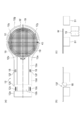
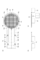
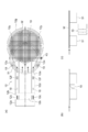
次に、図8~図16を参照して、ウェハチャック12によるウェハ搬送工程を説明する。図8~図16は、連続する工程を示している。図8~図11は、例えば故障解析後のウェハWをウェハ交換箇所(ウェハ搬送ロボット60の近傍)まで搬送する工程を示しており、図12は、ウェハ搬送ロボット60によるウェハ交換の工程を示しており、図13~図16は、新たなウェハWを載置台11まで搬送する工程を示している。なお、図8~図16の各図面において、同じ図番号の(a)~(c)(又は(a)~(b))は互いに同じタイミングの状態を示している。なお、以下ではX方向とは図の右方向(載置台11からウェハベース51に向かう方向)を、-X方向とは図の左方向(載置台11からウェハベース51に向かう方向とは反対方向)を、それぞれ示すとして説明する。
図8(a)に示されるように、いま、コントローラ50によるXステージ21の制御によって、ウェハWを保持するウェハチャック12が-X方向に移動している。なお、前提として、コントローラ50によるYステージ22の制御によって、ウェハ交換箇所の近傍に設けられたラチェット機構18,18のYの位置と、ウェハチャック12の孔部12f,12fのYの位置とは一致している。図8(a)に示される状態においては、ウェハチャック12の孔部12f,12fのXの位置が、ラチェット機構18,18のXの位置に到達していない。図8(b)に示されるように、ラチェット機構18にはばね力で上方向に力が加わっているところ、ラチェット機構18に孔部12fが到達する前段階においては、ラチェット機構18の上方向への力は第2部分12eの裏面に抑えられている。また、図8(c)に示されるように、図8(a)の状態においては、ウェハベース51の一部にウェハWの一部が既に載置されている。
ここから更にウェハチャック12が-X方向に移動すると、図9(a)に示されるように、ウェハベース51の中央とウェハWの中央とが一致するようにウェハベース51にウェハWが載置されると共に、ラチェット機構18,18とウェハチャック12の孔部12f,12fとが係合する(図9(b)参照)。ラチェット機構18は、バネ機構により孔部12fを通過し上方に飛び出すことによりリング部12dの-X方向への移動(動き)を阻害する。ラチェット機構18と孔部12fとが係合した状態においては、リング部12dの位置が固定され、リング部12dに係る構成(突出部12y,12yを含む)の位置が変化しなくなる。以降に、同じ方向にウェハチャック12が移動すると、ベース部12a及びコア部12bのみが同じ方向に移動し、リング部12dの位置は変化しない。このようなベース部12a及びコア部12bとリング部12dとの位置の相違は、弾性部材12cが延び縮みすることにより吸収される。
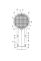
図10に示されるように、ベース部12a及びコア部12bが更に同じ-X方向に移動すると、コア部12bの先端に設けられた突出部12x,12xがウェハWから離間し、ウェハWの挟持状態が解除される。コントローラ50によるXステージ21の制御によって、コア部12bは、突出部12x,12xのオーバーハング内径よりも大きなスペースが開放される位置まで移動し停止する。
つづいて、図11(c)に示されるように、コントローラ50による制御によって、ウェハホルダ19が上昇しウェハWを裏面側から押し上げる。ウェハホルダ19が上昇することによりウェハホルダ19の斜面によってウェハWがスライドし、ウェハホルダ19の中心とウェハWの中心とが合致する位置にウェハWを載置することができる。
つづいて、図12(c)に示されるように、ウェハホルダ19が上昇した状態において、コントローラ50によってウェハ搬送ロボット60が制御されることにより、故障解析後のウェハWであるウェハW1のアンロード(取り外し)が実施され、つづいて、故障解析前のウェハWであるウェハW2のロードが実施される。なお、ウェハW2がロードされる際には、例えばノッチセンサ43によってウェハW2のノッチの場所が特定され、ウェハW2の傾きが調整されて、正しい角度にウェハW2がセットされる。図12(a)には、ウェハW(ウェハW1)がアンロードされた状態のウェハチャック12、ウェハベース51、及びウェハホルダ19が示されている。
つづいて、図13(c)に示されるように、コントローラ50による制御によって、ウェハホルダ19が下降しウェハベース51上にウェハWが載置される。ウェハホルダ19は、ウェハベース51よりも下方に退避する。
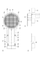
つづいて、図14(a)に示されるように、コントローラ50によるXステージ21の制御によって、ベース部12a及びコア部12bがX方向に移動し、突出部12x,12xがウェハWの周部に接触する。なお、この状態において、リング部12dは、ラチェット機構18,18とウェハチャック12の孔部12f,12fとが係合する(図14(b)参照)ことによってX方向への移動が規制されている。
つづいて、図15(a)に示されるように、コントローラ50によるXステージ21の制御によって、ベース部12a及びコア部12bがX方向にさらに移動し、突出部12x,12xがウェハWをX方向に押すことにより、リング部12dの突出部12y,12yにウェハWの周部が接触する。突出部12x,12x及び突出部12y,12yによって両側からウェハWに力がかかりウェハWが挟持されることにより、搬送中のウェハWが固定される。そして、この時点で、リング部12dにX方向の力がかかり始め、図15(b)に示されるように、ラチェット機構18,18とウェハチャック12の孔部12f,12fとの係合状態が解除される。すなわち、リング部12dがラチェット機構18から開放される。
そして、ウェハWの周部が突出部12x,12x,12y,12yによって挟持された状態で、図16(a)に示されるように、コントローラ50によるXステージ21の制御によって、ウェハチャック12がX方向に移動する。すなわち、ウェハチャック12は、ウェハベース51から離間し、載置台11に向かって移動する。ウェハチャック12の根本に設けられた弾性部材12cによって、ウェハWを左右(両側)から挟み込み挟持することができる。
次に、本実施形態に係る故障解析ユニット10の作用効果について、比較例に係る構成(図17参照)を比較しながら説明する。
故障解析ユニット10におけるウェハ搬送機構として、ウェハWを載置して搬送するウェハチャック12を含む構成が知られている。ウェハチャック12にウェハWを強固に保持する方法として、図17(a)に示されるように、テープ300でウェハチャック12にウェハWの表面側を固定する方法がある。テープ300は、高さが低い。そのため、ウェハWの表面側からプローブカード16の針16aをウェハWのパッドにタッチダウンさせる際において、ウェハエッジ近傍のチップまでアクセスが可能になる点で優位である。しかしながら、近年、複数枚のウェハWに対して自動で故障解析を実行すべく、ウェハ搬送ロボット60によってウェハカセット70からウェハチャック12にウェハWを移動させる場合があるところ、このようなウェハ搬送ロボット60を用いる場合には、ウェハチャック12にウェハWをテープ300で固定する方法は採用し難い。そこで、テープ300で固定する以外の構成で搬送中のウェハWを強固に保持する構成が求められている。
このような構成として、例えばウェハWの表面側に搬送中のウェハWを強固に保持する固定具を設ける構成を採用することが考えられる。しかしながら、例えば図17(b)に示されるように、比較的高さが高い固定具200aを用いた場合には、固定具200aの高さがプローブカード16の底面から針16aの先端までの高さよりも高くなってしまい、上述したタッチダウンが不可能になるおそれがある。また、例えば図17(c)に示されるように、比較的高さが低い固定具200bを用いた場合には、固定具200aのようにタッチダウン不可になることはないが、ウェハエッジ近傍においてプローブカード16の設計によっては干渉が生じるおそれがある。以上のように、ウェハ搬送機構においては、テープ以外の方法で搬送中のウェハWを強固に保持することが求められているものの、半導体故障解析装置の各機能を実現する上で、保持手段の位置及び厚み等に制限があり、適切な保持手段が見出されていない。
上述した課題を解決する構成として、本実施形態に係る故障解析ユニット10は、半導体故障解析装置においてウェハWを保持しながら搬送するウェハ搬送ユニットであって、所定の観察位置にウェハWを固定する載置台11と、観察位置までウェハWを保持しながら搬送するウェハチャック12と、を備え、ウェハチャック12は、ウェハWの側面と対向するように設けられた複数の保持部材(突出部12x,12x,12y,12y)を有し、複数の保持部材によってウェハWの周部を挟持することによりウェハWを保持する。
本実施形態に係る故障解析ユニット10では、ウェハWが固定される観察位置まで、ウェハチャック12によってウェハWが搬送される。そして、ウェハチャック12は、ウェハWの側面と対向するように設けられた複数の突出部12x,12x,12y,12yによってウェハWの周部を挟持する。このように、ウェハチャック12の突出部12x,12x,12y,12yがウェハWの側面からウェハWの周部を挟持する構成を採用することによって、搬送中のウェハWを強固に保持するための新たな構成をウェハWの裏面側及び表面側に設ける必要がない。このことにより、半導体故障解析装置の各機能を妨げることなく、搬送中のウェハWを適切に保持することができる。
複数の保持部材は、少なくとも4つの突出部12x,12x,12y,12yを含んで構成されていてもよい。これにより、ウェハWをより安定的に挟持することができる。
複数の保持部材は、ウェハWの周部に当接する複数の突出部12y,12yを含む第1の保持部材と、複数の突出部12x,12xを含む第2の保持部材とを有し、ウェハWを挟持する第1の保持部材がウェハWに与える力の方向と、ウェハWを挟持する第2の保持部材がウェハWに与える力の方向とは互いに反対の方向であってもよい。第1の保持部材がウェハWに与える力の方向と第2の保持部材がウェハWに与える力の方向とを互いに反対の方向とすることにより、第1の保持部材及び第2の保持部材によってウェハWを適切に挟持することができる。
上記の故障解析ユニット10は、第1の保持部材のみの位置を固定することにより、第1の保持部材及び第2の保持部材間の離間距離を変化させ、第1の保持部材及び第2の保持部材によるウェハWの挟持状態を解除可能に構成されたラチェット機構18を更に備えていてもよい。このような構成によれば、第1の保持部材のみの位置を固定するという簡易な構成によって、ウェハWの挟持状態を適切に解除する(ウェハWを開放する)ことができる。
ウェハチャック12は、ベース部12aと、弾性部材12cを介してベース部12aに接続された第1部分12kと、第1部分12kに連続すると共に互いに対向しながらX方向に延びる一対の第2部分12e,12eと、一対の第2部分12eの先端に連続すると共にウェハを収容する収容スペースを区画するようにリング状に形成された第3部分12gと、を含むリング部12dと、ベース部12aに連続すると共に一対の第2部分12e,12e間においてX方向に延びるコア部12bと、を有し、リング部12dの第3部分12gには、収容スペースに向かって突出した突出部12y,12yが設けられており、コア部12bの先端には、収容スペースに向かって突出した突出部12x,12xが設けられており、リング部12dの一対の第2部分12eには、ラチェット機構18と係合可能に構成された孔部12fが形成されており、ラチェット機構18は、孔部12fと係合することにより、リング部12dの位置を固定して突出部12y,12yの位置を固定してもよい。このような構成によれば、収容スペースに向かって突出した突出部12y,12yと突出部12x,12xとによって、ウェハWが適切に挟持される。そして、リング部12dの一対の第2部分12eの孔部12fがラチェット機構18と係合することにより、リング部12dが固定され突出部12y,12yの位置が固定される。このような場合において、リング部12dとベース部12aとは弾性部材12cを介して接続されていることから、弾性部材12cが延びることによって、リング部12dの位置が固定された状態においてもベース部12a及びベース部12aに連続するコア部12bは変位可能となる。リング部12dの位置が固定された状態でコア部12bが収容スペースから離れる方向に変位することにより、リング部12dに設けられた突出部12y,12yとコア部12bに設けられた突出部12x,12xとの離間距離が大きくなり、突出部12y,12y及び突出部12x,12xによるウェハWの挟持状態が解除されることになる。以上のように、上述した構成によって、ウェハWの適切な挟持及び解除(開放)を容易に行うことができる。また、ウェハのチャック/アンチャックはXステージの動作で実現しており、別のチャック/アンチャック駆動機構を設けなくともよい。これにより、ウェハロード/アンロードシステムとしての信頼性の向上を図ることができる。
以上、本発明の実施形態について説明したが本発明は上記実施形態に限定されない。例えば、上記実施形態では、保持部材として少なくとも4つの突出部が設けられているとして説明したが、図18に示されるように、突出部が3つであってもよい。すなわち、図18(a)及び図18(b)に示されるウェハチャックでは、コア部512bの先端に2つの突出部512x,512xが設けられており、また、リング部512dの第3部分512gに1つの突出部512yが設けられている。突出部512x,512x,512yが設けられている位置については特に限られないが、例えば突出部512x,512xが設けられている位置は、Y方向において、突出部512yが設けられている位置よりも外側である。
10…故障解析ユニット(ウェハ搬送ユニット)、11…載置台(固定部)、12…ウェハチャック(搬送部)、12a…ベース部、12b…コア部、12c…弾性部材、12d…リング部、12e…第2部分、12f…孔部、12g…第3部分、12k…第1部分、12x,12x,12y,12y…突出部、18…ラチェット機構(歯止め部)、19…ウェハホルダ、21…Xステージ、22…Yステージ、40…パフォーマンスボード、41…コネクタボード、42…ポゴタワー、43…ノッチセンサ、50…コントローラ、51…ウェハベース、60…ウェハ搬送ロボット、61…ハンド、70…ウェハカセット、80…固浸レンズ、200a,200b…固定具、300…テープ、512b…コア部、512d…リング部、512x…突出部、512y…突出部、W…ウェハ。
Claims (7)
- 半導体故障解析装置においてウェハを保持しながら搬送するウェハ搬送ユニットであって、
所定の観察位置にウェハを固定する固定部と、
前記観察位置まで前記ウェハを保持しながら搬送する搬送部と、を備え、
前記搬送部は、前記ウェハの側面と対向するように設けられた複数の保持部材を有し、前記複数の保持部材によって前記ウェハの周部を挟持することにより前記ウェハを保持する、ウェハ搬送ユニット。 - 前記複数の保持部材は、前記ウェハの周部に当接する少なくとも3つの突出部を含んで構成されている、請求項1記載のウェハ搬送ユニット。
- 前記複数の保持部材は、少なくとも4つの前記突出部を含んで構成されている、請求項2記載のウェハ搬送ユニット。
- 前記複数の保持部材は、前記ウェハの周部に当接する一又は複数の突出部を含む第1の保持部材と、一又は複数の前記突出部を含む第2の保持部材とを有し、
前記ウェハを挟持する前記第1の保持部材が前記ウェハに与える力の方向と、前記ウェハを挟持する前記第2の保持部材が前記ウェハに与える力の方向とは互いに反対の方向である、請求項1~3のいずれか一項記載のウェハ搬送ユニット。 - 前記第1の保持部材及び前記第2の保持部材のいずれか一方のみの位置を固定することにより、前記第1の保持部材及び前記第2の保持部材間の離間距離を変化させ、前記第1の保持部材及び前記第2の保持部材による前記ウェハの挟持状態を解除可能に構成された歯止め部を更に備える、請求項4記載のウェハ搬送ユニット。
- 前記搬送部は、
ベース部と、
弾性部材を介して前記ベース部に接続された第1部分と、前記第1部分に連続すると共に互いに対向しながら第1方向に延びる一対の第2部分と、前記一対の第2部分の先端に連続すると共にウェハを収容する収容スペースを区画するようにリング状に形成された第3部分と、を含むリング部と、
前記ベース部に連続すると共に前記一対の第2部分間において第1方向に延びるコア部と、を有し、
前記リング部の前記第3部分には、前記収容スペースに向かって突出した前記第1の保持部材が設けられており、
前記コア部の先端には、前記収容スペースに向かって突出した前記第2の保持部材が設けられており、
前記リング部の前記一対の第2部分には、前記歯止め部と係合可能に構成された孔部が形成されており、
前記歯止め部は、前記孔部と係合することにより、前記リング部の位置を固定して前記第1の保持部材の位置を固定する、請求項5記載のウェハ搬送ユニット。 - 半導体故障解析装置においてウェハを保持しながら搬送するウェハ搬送方法であって、
前記ウェハの側面と対向するように設けられた複数の保持部材によって前記ウェハの周部を挟持する工程と、
前記複数の保持部材によって前記ウェハの周部を挟持した状態で、前記ウェハを所定の観察位置まで搬送する工程と、を含むウェハ搬送方法。
Priority Applications (4)
| Application Number | Priority Date | Filing Date | Title |
|---|---|---|---|
| KR1020227012221A KR102784451B1 (ko) | 2020-01-23 | 2020-11-09 | 웨이퍼 반송 유닛 및 웨이퍼 반송 방법 |
| CN202080094175.7A CN115023799B (zh) | 2020-01-23 | 2020-11-09 | 晶圆搬送单元及晶圆搬送方法 |
| EP20914993.9A EP4044215A4 (en) | 2020-01-23 | 2020-11-09 | Wafer conveyance unit and wafer conveyance method |
| US17/772,596 US12347718B2 (en) | 2020-01-23 | 2020-11-09 | Wafer conveyance unit and wafer conveyance method |
Applications Claiming Priority (2)
| Application Number | Priority Date | Filing Date | Title |
|---|---|---|---|
| JP2020009273A JP7454385B2 (ja) | 2020-01-23 | 2020-01-23 | ウェハ搬送ユニット及びウェハ搬送方法 |
| JP2020-009273 | 2020-01-23 |
Publications (1)
| Publication Number | Publication Date |
|---|---|
| WO2021149330A1 true WO2021149330A1 (ja) | 2021-07-29 |
Family
ID=76993327
Family Applications (1)
| Application Number | Title | Priority Date | Filing Date |
|---|---|---|---|
| PCT/JP2020/041755 Ceased WO2021149330A1 (ja) | 2020-01-23 | 2020-11-09 | ウェハ搬送ユニット及びウェハ搬送方法 |
Country Status (7)
| Country | Link |
|---|---|
| US (1) | US12347718B2 (ja) |
| EP (1) | EP4044215A4 (ja) |
| JP (1) | JP7454385B2 (ja) |
| KR (1) | KR102784451B1 (ja) |
| CN (1) | CN115023799B (ja) |
| TW (1) | TWI849263B (ja) |
| WO (1) | WO2021149330A1 (ja) |
Families Citing this family (2)
| Publication number | Priority date | Publication date | Assignee | Title |
|---|---|---|---|---|
| CN116184176A (zh) * | 2023-03-30 | 2023-05-30 | 苏州索莱能智能科技有限公司 | 射频芯片测试设备 |
| DE102024117724A1 (de) * | 2024-06-24 | 2025-12-24 | Ams-Osram International Gmbh | Vorrichtung, wafer und verfahren zur herstellung eines elektronischen bauelements |
Citations (5)
| Publication number | Priority date | Publication date | Assignee | Title |
|---|---|---|---|---|
| WO2006057050A1 (ja) * | 2004-11-29 | 2006-06-01 | Hirata Corporation | 基板把持装置 |
| US20100315617A1 (en) | 2009-06-12 | 2010-12-16 | Semicaps Pte Ltd | Wafer stage |
| JP2011119348A (ja) * | 2009-12-01 | 2011-06-16 | Kawasaki Heavy Ind Ltd | エッジグリップ装置、及びそれを備えるロボット。 |
| JP2018111200A (ja) * | 2016-12-06 | 2018-07-19 | ジャビル インク | エンドエフェクターを供給するための器具、システム、及び方法 |
| JP2018170418A (ja) * | 2017-03-30 | 2018-11-01 | 東京エレクトロン株式会社 | 検査システム、ウエハマップ表示器、ウエハマップ表示方法、およびコンピュータプログラム |
Family Cites Families (12)
| Publication number | Priority date | Publication date | Assignee | Title |
|---|---|---|---|---|
| JPS5244566B2 (ja) * | 1974-03-05 | 1977-11-09 | ||
| US7281741B2 (en) * | 2001-07-13 | 2007-10-16 | Semitool, Inc. | End-effectors for handling microelectronic workpieces |
| US7226269B2 (en) * | 2004-01-15 | 2007-06-05 | Applied Materials, Inc. | Substrate edge grip apparatus |
| JP2007281325A (ja) * | 2006-04-11 | 2007-10-25 | Nec Electronics Corp | ウエハ保持治具およびウエハ保持方法 |
| JP5066393B2 (ja) | 2007-06-06 | 2012-11-07 | 株式会社日立ハイテクノロジーズ | 異物・欠陥検査・観察システム |
| JP5244566B2 (ja) * | 2008-12-02 | 2013-07-24 | 株式会社東芝 | テンプレート洗浄方法、洗浄システム、及び洗浄装置 |
| JP2013033809A (ja) * | 2011-08-01 | 2013-02-14 | Tokyo Electron Ltd | ウエハ搬送装置 |
| JP2017191124A (ja) * | 2016-04-11 | 2017-10-19 | 株式会社ニコン | 基板保持部材、搬送装置及び方法、露光装置及び方法、露光システム、並びにデバイス製造方法 |
| JP6757646B2 (ja) * | 2016-10-27 | 2020-09-23 | 川崎重工業株式会社 | 基板把持ハンド及びそれを備える基板搬送装置 |
| JP7064885B2 (ja) | 2018-01-05 | 2022-05-11 | 東京エレクトロン株式会社 | 基板把持機構、基板搬送装置及び基板処理システム |
| CN208093519U (zh) * | 2018-03-27 | 2018-11-13 | 深圳市佳思特光电设备有限公司 | 半导体封装一体机的自动供料机构 |
| JP7205966B2 (ja) * | 2018-06-29 | 2023-01-17 | 川崎重工業株式会社 | 基板搬送装置及びその運転方法 |
-
2020
- 2020-01-23 JP JP2020009273A patent/JP7454385B2/ja active Active
- 2020-11-09 CN CN202080094175.7A patent/CN115023799B/zh active Active
- 2020-11-09 EP EP20914993.9A patent/EP4044215A4/en active Pending
- 2020-11-09 WO PCT/JP2020/041755 patent/WO2021149330A1/ja not_active Ceased
- 2020-11-09 KR KR1020227012221A patent/KR102784451B1/ko active Active
- 2020-11-09 US US17/772,596 patent/US12347718B2/en active Active
- 2020-11-27 TW TW109141698A patent/TWI849263B/zh active
Patent Citations (5)
| Publication number | Priority date | Publication date | Assignee | Title |
|---|---|---|---|---|
| WO2006057050A1 (ja) * | 2004-11-29 | 2006-06-01 | Hirata Corporation | 基板把持装置 |
| US20100315617A1 (en) | 2009-06-12 | 2010-12-16 | Semicaps Pte Ltd | Wafer stage |
| JP2011119348A (ja) * | 2009-12-01 | 2011-06-16 | Kawasaki Heavy Ind Ltd | エッジグリップ装置、及びそれを備えるロボット。 |
| JP2018111200A (ja) * | 2016-12-06 | 2018-07-19 | ジャビル インク | エンドエフェクターを供給するための器具、システム、及び方法 |
| JP2018170418A (ja) * | 2017-03-30 | 2018-11-01 | 東京エレクトロン株式会社 | 検査システム、ウエハマップ表示器、ウエハマップ表示方法、およびコンピュータプログラム |
Non-Patent Citations (1)
| Title |
|---|
| See also references of EP4044215A4 |
Also Published As
| Publication number | Publication date |
|---|---|
| KR102784451B1 (ko) | 2025-03-21 |
| KR20220131890A (ko) | 2022-09-29 |
| US20220406644A1 (en) | 2022-12-22 |
| TW202129821A (zh) | 2021-08-01 |
| CN115023799B (zh) | 2026-04-21 |
| US12347718B2 (en) | 2025-07-01 |
| CN115023799A (zh) | 2022-09-06 |
| JP2021118224A (ja) | 2021-08-10 |
| EP4044215A4 (en) | 2024-01-24 |
| JP7454385B2 (ja) | 2024-03-22 |
| EP4044215A1 (en) | 2022-08-17 |
| TWI849263B (zh) | 2024-07-21 |
Similar Documents
| Publication | Publication Date | Title |
|---|---|---|
| TWI797879B (zh) | 具有堆疊式封裝(pop)結構的裝置之攜載式大量系統級測試技術 | |
| KR101208137B1 (ko) | 프로브 장치 | |
| US9671452B2 (en) | Substrate inspection apparatus and probe card transferring method | |
| KR102402669B1 (ko) | 접속 구조체 및 접속 구조체 모듈, 및 이를 이용하는 프로브 카드 어셈블리 및 웨이퍼 테스트 장치 | |
| US20090179366A1 (en) | Apparatus for supporting a substrate during semiconductor processing operations | |
| JP2014075420A (ja) | ウエハ取り付け方法及びウエハ検査装置 | |
| JP6114060B2 (ja) | 基板搬送装置、基板受渡位置確認方法及び基板処理システム | |
| KR101915878B1 (ko) | 기판 주고받음 위치의 교시 방법 및 기판 처리 시스템 | |
| US20130195587A1 (en) | Wafer transfer device | |
| CN110692129B (zh) | 用于测试半导体装置的设备和方法 | |
| JP2021118224A (ja) | ウェハ搬送ユニット及びウェハ搬送方法 | |
| US7458469B2 (en) | Substrate transfer apparatus and method, and storage medium | |
| TWI839869B (zh) | 基板處理裝置及基板處理方法 | |
| KR101199718B1 (ko) | 발광 소자 검사 장치 | |
| US12136560B1 (en) | Workpiece transfer apparatus | |
| JP3205980U (ja) | フォーク用位置決め治具および基板を支持するフォーク並びに複数のフォークを備えた基板を搬送する基板搬送装置 | |
| KR102326005B1 (ko) | 반도체 소자 픽업 장치 | |
| US12078673B1 (en) | Workpiece positioning mechanism and workpiece inspection apparatus | |
| JPH0384944A (ja) | 半導体検査装置及び検査方法 | |
| US20260098897A1 (en) | Carrier module, tray, and test handler | |
| WO2018157718A1 (zh) | 应用静电载具测试半导体制品的机构 | |
| WO2018159207A1 (ja) | 検査システム | |
| JP2024126670A (ja) | 基板保持装置 | |
| JP2018088477A (ja) | 基板位置決め装置 | |
| KR20020075584A (ko) | 플레이트 어셈블리 |
Legal Events
| Date | Code | Title | Description |
|---|---|---|---|
| 121 | Ep: the epo has been informed by wipo that ep was designated in this application |
Ref document number: 20914993 Country of ref document: EP Kind code of ref document: A1 |
|
| ENP | Entry into the national phase |
Ref document number: 2020914993 Country of ref document: EP Effective date: 20220511 |
|
| NENP | Non-entry into the national phase |
Ref country code: DE |
|
| WWG | Wipo information: grant in national office |
Ref document number: 17772596 Country of ref document: US |