WO2021149558A1 - 点灯回路および車両用灯具 - Google Patents
点灯回路および車両用灯具 Download PDFInfo
- Publication number
- WO2021149558A1 WO2021149558A1 PCT/JP2021/000853 JP2021000853W WO2021149558A1 WO 2021149558 A1 WO2021149558 A1 WO 2021149558A1 JP 2021000853 W JP2021000853 W JP 2021000853W WO 2021149558 A1 WO2021149558 A1 WO 2021149558A1
- Authority
- WO
- WIPO (PCT)
- Prior art keywords
- temperature
- drive current
- light source
- semiconductor light
- current
- Prior art date
- Legal status (The legal status is an assumption and is not a legal conclusion. Google has not performed a legal analysis and makes no representation as to the accuracy of the status listed.)
- Ceased
Links
Images




Classifications
-
- H—ELECTRICITY
- H05—ELECTRIC TECHNIQUES NOT OTHERWISE PROVIDED FOR
- H05B—ELECTRIC HEATING; ELECTRIC LIGHT SOURCES NOT OTHERWISE PROVIDED FOR; CIRCUIT ARRANGEMENTS FOR ELECTRIC LIGHT SOURCES, IN GENERAL
- H05B45/00—Circuit arrangements for operating light-emitting diodes [LED]
- H05B45/10—Controlling the intensity of the light
- H05B45/18—Controlling the intensity of the light using temperature feedback
-
- F—MECHANICAL ENGINEERING; LIGHTING; HEATING; WEAPONS; BLASTING
- F21—LIGHTING
- F21S—NON-PORTABLE LIGHTING DEVICES; SYSTEMS THEREOF; VEHICLE LIGHTING DEVICES SPECIALLY ADAPTED FOR VEHICLE EXTERIORS
- F21S43/00—Signalling devices specially adapted for vehicle exteriors, e.g. brake lamps, direction indicator lights or reversing lights
- F21S43/10—Signalling devices specially adapted for vehicle exteriors, e.g. brake lamps, direction indicator lights or reversing lights characterised by the light source
- F21S43/13—Signalling devices specially adapted for vehicle exteriors, e.g. brake lamps, direction indicator lights or reversing lights characterised by the light source characterised by the type of light source
- F21S43/14—Light emitting diodes [LED]
-
- F—MECHANICAL ENGINEERING; LIGHTING; HEATING; WEAPONS; BLASTING
- F21—LIGHTING
- F21S—NON-PORTABLE LIGHTING DEVICES; SYSTEMS THEREOF; VEHICLE LIGHTING DEVICES SPECIALLY ADAPTED FOR VEHICLE EXTERIORS
- F21S45/00—Arrangements within vehicle lighting devices specially adapted for vehicle exteriors, for purposes other than emission or distribution of light
- F21S45/10—Protection of lighting devices
-
- F—MECHANICAL ENGINEERING; LIGHTING; HEATING; WEAPONS; BLASTING
- F21—LIGHTING
- F21S—NON-PORTABLE LIGHTING DEVICES; SYSTEMS THEREOF; VEHICLE LIGHTING DEVICES SPECIALLY ADAPTED FOR VEHICLE EXTERIORS
- F21S45/00—Arrangements within vehicle lighting devices specially adapted for vehicle exteriors, for purposes other than emission or distribution of light
- F21S45/40—Cooling of lighting devices
- F21S45/47—Passive cooling, e.g. using fins, thermal conductive elements or openings
-
- H—ELECTRICITY
- H05—ELECTRIC TECHNIQUES NOT OTHERWISE PROVIDED FOR
- H05B—ELECTRIC HEATING; ELECTRIC LIGHT SOURCES NOT OTHERWISE PROVIDED FOR; CIRCUIT ARRANGEMENTS FOR ELECTRIC LIGHT SOURCES, IN GENERAL
- H05B45/00—Circuit arrangements for operating light-emitting diodes [LED]
- H05B45/30—Driver circuits
- H05B45/345—Current stabilisation; Maintaining constant current
-
- H—ELECTRICITY
- H05—ELECTRIC TECHNIQUES NOT OTHERWISE PROVIDED FOR
- H05B—ELECTRIC HEATING; ELECTRIC LIGHT SOURCES NOT OTHERWISE PROVIDED FOR; CIRCUIT ARRANGEMENTS FOR ELECTRIC LIGHT SOURCES, IN GENERAL
- H05B45/00—Circuit arrangements for operating light-emitting diodes [LED]
- H05B45/30—Driver circuits
- H05B45/395—Linear regulators
Definitions
- This disclosure relates to lamps used in automobiles and the like.
- luminous flux maintenance rate For vehicle lighting equipment, regulations regarding luminous flux are stipulated.
- LR5 which is an interchangeable LED light source for automobile signal lights
- UN (UN) regulations the luminous flux at the time of stabilization is 102 to 138 lm
- the ratio of the luminous flux after 1 minute of lighting to the luminous flux after 30 minutes of lighting is It is required to be 80% or more.
- FIG. 1 is a diagram showing an example of the relationship between the temperature of the LED and the luminous flux.
- the brightness when the same drive current is supplied to the semiconductor light source decreases as the temperature rises.
- FIG. 2 is a diagram showing the operation of a vehicle lamp that controls a semiconductor light source with a constant current.
- Time t 0 is the lighting start time, and the drive current I LED flowing through the semiconductor light source is stabilized to a predetermined amount of current.
- the temperature T of the semiconductor light source rises and stabilizes at the point where heat generation and heat dissipation are balanced.
- the semiconductor light source lights brightly when the temperature is low immediately after the start of lighting, but the amount of light decreases as the temperature rises over time.
- This disclosure has been made in view of such a problem, and one of the exemplary purposes of the embodiment is to improve the stability of the luminous flux of a vehicle lamp.
- the lighting circuit includes a warming element whose electrical state changes according to the temperature T of the semiconductor light source, and a constant current driver that generates a drive current according to the temperature T.
- the maximum value of the temperature differentiation of the drive current in the first temperature range T 0 to T 1 from the reference temperature T 0 to the first temperature T 1 (T 1 > T 0 ) is the first temperature T 1 to the second temperature T 2 It is smaller than the maximum value of the temperature differential of the drive current in the second temperature range up to (T 2 > T 1).
- This vehicle lamp includes a semiconductor light source and a lighting circuit that supplies a drive current to the semiconductor light source.
- the amount of change in the drive current during the start period immediately after the start of lighting is smaller than the amount of increase in the drive current during the stable period following the start period.
- the stability of the luminous flux of the vehicle lamp can be improved.
- FIG. 10 (a) to 10 (d) are diagrams showing an LED socket which is an example of a vehicle lamp.
- 11 (a) and 11 (b) are diagrams showing the temperature characteristics of the drive current I LED according to the first and second modifications. It is a circuit diagram of the constant current driver which concerns on modification 3.
- the lighting circuit includes a warming element whose electrical state changes according to the temperature T of the semiconductor light source, and a constant current driver that generates a drive current according to the temperature T.
- the maximum value of the temperature differentiation of the drive current in the first temperature range T 0 to T 1 from the reference temperature T 0 to the first temperature T 1 (T 1 > T 0 ) is the first temperature T 1 to the second temperature T 2 It is smaller than the maximum value of the temperature differential of the drive current in the second temperature range up to (T 2 > T 1).
- the temperature of the semiconductor light source rises from the reference temperature to the first temperature in the start period (several tens of seconds to several minutes) immediately after the start of lighting, and in the subsequent stable period, the temperature rises from the first temperature to the second temperature. Ascend to.
- the first temperature T 1 may be determined based on the temperature at the start time of the stable period.
- the second temperature T 2 may be determined based on the steady temperature during the stable period.
- the starting point of the stable period may be one minute after the start of lighting.
- the second temperature may be determined based on the temperature 30 minutes after the start of lighting.
- both the temperature derivative of the drive current in the first temperature range and the temperature derivative of the drive current in the second temperature range may be positive.
- the temperature derivative of the drive current may be negative in the first temperature range and the temperature derivative of the drive current may be positive in the second temperature range.
- the drive current may decrease in a third range above the third temperature T 3 (T 3 > T 2). As a result, temperature derating can be realized.
- the constant current driver is provided in series between a current source having a current setting terminal and generating a drive current inversely proportional to the impedance of the circuit connected to the current setting terminal, and between the current setting terminal and ground. It may also include a first resistor and a second resistor, and an NTC (negative temperature coefficient) thermistor provided in parallel with the second resistor.
- the vehicle lamp according to the embodiment includes a semiconductor light source and the above-mentioned lighting circuit that supplies a drive current to the semiconductor light source.
- the amount of change in the drive current during the period from the start of lighting of the semiconductor light source to 1 minute after the start of lighting is smaller than the amount of increase in the drive current during the period from 1 minute to 30 minutes after the start of lighting of the semiconductor light source.
- the "state in which the member A is connected to the member B” means that the member A and the member B are physically directly connected, and that the member A and the member B are electrically connected to each other. It also includes the case of being indirectly connected via other members, which does not substantially affect the connection state, or does not impair the functions and effects performed by the combination thereof.
- a state in which the member C is provided between the member A and the member B means that the member A and the member C, or the member B and the member C are directly connected, and their electricity. It also includes the case of being indirectly connected via other members, which does not substantially affect the connection state, or does not impair the functions and effects produced by the combination thereof.
- the reference numerals attached to electric signals such as voltage signals and current signals, or circuit elements such as resistors and capacitors have their respective voltage values, current values, resistance values, and capacitance values as required. It shall be represented.
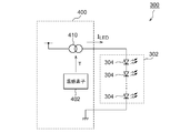
- FIG. 3 is a block diagram of a vehicle lamp 300 including the lighting circuit 400 according to the embodiment.
- the vehicle lamp 300 includes a semiconductor light source 302 and a lighting circuit 400.
- the semiconductor light source 302 includes one or a plurality of light emitting elements 304 connected in series and / or in parallel.
- the light emitting element 304 for example, an LED is suitable, but the present invention is not limited to this.
- the vehicle lamp 300 may be, for example, a stop lamp or a tail lamp, and the semiconductor light source 302 may be a red LED.
- One aspect of the vehicle lamp 300 is an LED socket in which the semiconductor light source 302 and the lighting circuit 400 are housed in one package, and has a shape that can be attached to and detached from a lamp body (not shown).
- the lighting circuit 400 mainly includes a warming element 402 and a constant current driver 410.
- the warming element 402 is provided to detect the temperature T of the semiconductor light source 302, and its electrical state changes according to the temperature T of the semiconductor light source 302.
- the electrical state of the warming element refers to the impedance of the warming element, its voltage drop, the current flowing through it, the voltage at one end thereof, and the like.
- the warming element 622 can directly or indirectly monitor the temperature of the semiconductor light source 302.
- the warming element 622 may be directly attached to the semiconductor light source 302, or adjacent to or close to the semiconductor light source 302. It may be attached to a heat sink to which the semiconductor light source 302 is attached.
- the constant current driver 410 generates a drive current I LED corresponding to the temperature T detected by the warming element 402.
- FIG. 3 shows a form in which the constant current driver 410 sources (exhausts) the drive current I LED , but the present invention is not limited to this, and the constant current driver 410 may sink the drive current I LED.
- FIG. 4 is a diagram showing an example of the temperature characteristics of the drive current I LED generated by the constant current driver 410.
- the reference temperature T 0 , the first temperature T 1 (T 1 > T 0 ), and the second temperature T 2 (T 2 > T 1 ) are set, and the reference temperature T 0 to the first temperature T 1 (T 1 > T 0 ) are set.
- the first temperature range T 0 to T 1 , and the first temperature T 1 to the second temperature T 2 are referred to as the second temperature range.
- the reference temperature T 0 is the temperature at the start of lighting, and is typically room temperature (25 to 30 degrees).
- the first temperature T 1 is the temperature at the starting point of the stable period.
- the second temperature T 2 is a steady temperature during a stable period when a sufficient time has elapsed from the start of lighting.
- a third temperature T 3 higher than the second temperature T 2 is defined. Exceeds the third temperature T 3, the drive current I LED decreases. This is the so-called temperature derating.
- the third temperature T 3 is set to 90 ° C. or higher, for example 105 ° C.
- the above is the configuration of the vehicle lamp 300.
- the features and advantages of the vehicle lamp 300 will be clarified by comparison with comparative technology. Therefore, before explaining the operation of the vehicle lamp 300, a comparative technique will be described.
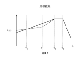
- FIG. 5 is a diagram showing the temperature characteristics of the drive current I LED in the comparative technique.
- the drive current I LED increases with a constant inclination as the temperature rises.
- T 1 and T 2 correspond to the first temperature T 1 and the second temperature T 2 in FIG. That is, in the comparative technique, the temperature derivative dI LED / dT of the drive current I LED in the first temperature range T 0 to T 1 , that is, the inclination is the temperature derivative or inclination of the drive current I LED in the second temperature range T 1 to T 2.
- the temperature characteristics of FIG. 4 are shown by alternate long and short dash lines.
- the correction factor of the drive current I LED in the first temperature range T 0 to T 1 is smaller than that in the comparative technique, and the drive current I in the second temperature range T 1 to T 2 is small.
- the LED correction factor is increasing.
- FIG. 6 is an operation waveform diagram of a vehicle lamp according to the comparative technique.
- the waveform of the prior art is shown as an alternate long and short dash line. It is assumed that the temperature T of the semiconductor light source transitions in the same manner as in FIG. In the comparative technique, the drive current I LED increases as the temperature rises over time. As a result, the attenuation of the luminous flux after time t 0 is slower than that of the comparative technique.
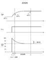
- FIG. 7 is an operation waveform diagram of the vehicle lamp 300 according to the embodiment.
- the waveform of the comparative technique is also shown as an alternate long and short dash line.
- the correction factor (increase amount) of the drive current I LED in the start period corresponding to the first temperature range T 0 to T 1 is smaller than that of the comparative technique (dashed line). Therefore, in the embodiment, the reduction rate of the luminous flux during the start period is larger than that of the comparative technique.
- the correction factor (correction amount) of the drive current I LED in the stable period corresponding to the second temperature range T 1 to T 2 is larger than that of the comparison technique, and finally decreases to the same luminous flux as that of the comparison technique. ..
- the lighting circuit 400 is configured so that the amount of change in the drive current I LED in the start period immediately after the start of lighting is smaller than the amount of increase in the drive current I LED in the stable period.
- the luminous flux maintenance rate in the embodiment and the luminous flux maintenance rate in the comparative technique are compared. It is assumed that the luminous flux at time t 2 when a sufficient time has passed from the start of lighting is S 2 in both the embodiment and the comparative technique.
- S 1 be the luminous flux of the embodiment at the start point t 1 of the stable period
- S 1 ′ be the luminous flux of the comparative technique.
- the luminous flux maintenance rate ⁇ of the embodiment is S 2 / S 1 x 100 (%)
- the luminous flux maintenance rate ⁇ 'of the comparative technology is S 2 / S 1 ' ⁇ 100 (%) Is. ⁇ 'Because there is satisfied, ⁇ ⁇ S 1>' S 1 becomes. That is, according to the embodiment, it is possible to obtain a luminous flux maintenance rate even higher than that of the comparative technique.
- the above is the operation of the vehicle lamp 300.
- the stability of the amount of light can be improved while ensuring the reliability of the semiconductor light source 302.
- the temperature dependence of the brightness of the red LED is remarkable as compared with other elements. Therefore, by applying the present invention to a stop lamp or a tail lamp, the commercial value can be increased.
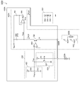
- FIG. 8 is a block diagram of the vehicle lamp 300A according to the embodiment.
- the constant current driver 410A includes a current source 420A and a reference voltage generation circuit 430.
- the main part of the lighting circuit 400A is integrated in one semiconductor chip.
- the reference voltage generation circuit 430 generates a reference voltage V REF that is substantially constant in the normal range and decreases with temperature T in a high temperature range higher than the third temperature T 3.
- the lighting circuit 400A is provided with a current setting terminal (current setting pin) RSET.
- An external circuit component can be connected to the current setting terminal RSET.
- the current source 420A generates a drive current I LED that is proportional to the reference voltage V REF and inversely proportional to the impedance (resistance value) R SET of the temperature detection circuit 444 connected to the current setting terminal. I LED ⁇ V REF / R SET
- the temperature detection circuit 444 is an NTC (negative temperature coefficient) thermistor provided in parallel with the first resistor R21 and the second resistor R22 provided in series between the current setting terminal RSET and the ground, and the second resistor R22.
- the second thermistor 402b and the like may be included.
- the I / V conversion circuit 450 converts the reference current I REF into a dimming voltage V DIM .
- the reference voltage generation circuit 430 includes a voltage divider circuit 432 and a clamp circuit 434.
- the voltage dividing circuit 432 divides the power supply voltage Vcc and generates a reference voltage V REF.
- the clamp circuit 434 clamps the reference voltage V REF below the upper limit voltage corresponding to the temperature T.
- the reference voltage V REF0 when the clamp circuit 434 is ignored is expressed by the following equation.
- V REF0 V CC x R51 / (R51 + R52)
- the clamp circuit 434 includes a first transistor Q1, a first resistor R1, and a first thermistor 402a.
- the first transistor Q1 is a PNP type bipolar transistor, and is provided between the output node of the voltage dividing circuit 432 and the ground.
- the first resistor R1 and the warming element 402 are second temperature detection units, generate a first detection signal Va that changes significantly according to the temperature of the semiconductor light source 302 in a high temperature range, and the first transistor according to the temperature. Bias the control terminal (base) of Q1.
- a P-channel MOSFET may be used as the first transistor Q1.
- a diode that receives the reference voltage V REF at the anode and receives the first detection signal Va may be provided at the cathode.
- the first thermistor 402a determines the inclination of the drive current I LED mainly in the high temperature range.
- the resistance value Ra of the first thermistor 402a has a negative temperature coefficient (NTC: Negative Temperature Coefficient).
- NTC Negative Temperature Coefficient
- V REF V REF0 , which is a constant value independent of the temperature.
- the I / V conversion circuit 450 includes a third resistor R3.
- the third resistor R3 is provided on the path of the reference current I REF.
- the dimming voltage V DIM responds to the voltage drop of the third resistor R3.
- V DIM V BAT- R3 x I REF
- the current source 420A is a source type, includes a resistor R4, a transistor M4, and an operational amplifier 412, and generates a drive current I LED proportional to the dimming voltage V DIM.
- I LED I REF x R3 / R4
- both the stability and reliability of the luminous flux of the semiconductor light source can be achieved.
- FIG. 10 (a) to 10 (d) are diagrams showing an LED socket 700 which is an example of a vehicle lamp 300.
- FIG. 10A is a perspective view of the appearance of the LED socket 700.
- 10 (b) shows a front view of the LED socket 700
- FIG. 10 (c) shows a plan view of the LED socket 700
- FIG. 10 (c) shows a bottom view of the LED socket 700.
- the housing 702 has a shape that can be attached to and detached from a lamp body (not shown).
- a plurality of light emitting elements 304 constituting the semiconductor light source 302 are mounted in the central portion, and they are covered with a transparent cover 704.
- the components of the lighting circuit 600 are mounted on the board 710.
- the plurality of light emitting elements 304 are red LED chips and are used as stop lamps and rear fog lamps.
- the light emitting element for the tail lamp is mounted in the center of the plurality of light emitting elements 304, and the lighting circuit for the tail lamp is mounted on the substrate 710.
- the first input voltage V IN1 is supplied to the pin 723 via a switch, and the ground voltage is supplied to the pin 721.
- the pin 722 is supplied with a second input voltage V IN2 that becomes high when the tail lamp is lit. Pins 721 to 723 penetrate the inside of the housing 702, and one end thereof is connected to the wiring pattern of the substrate 710.
- FIG. 11A is a diagram showing the temperature characteristics of the drive current I LED according to the first modification.
- the drive current I LED is flat in the first temperature range T 0 to T 1 , and its inclination is very small.
- FIG. 11B is a diagram showing the temperature characteristics of the drive current I LED according to the second modification.
- the drive current I LED decreases with increasing temperature, and therefore the differential value can be negative.
- the luminous flux at the start time of the stable period when the temperature reaches T 1 can be further reduced, and the luminous flux maintenance rate during the stable period can be improved.
- FIG. 12 is a circuit diagram of the constant current driver 410B according to the third modification.
- the clamp circuit 434B includes a current suction (sink) type buffer 436 including an operational amplifier OA1 and a diode D1 in place of the first transistor Q1 in FIG.
- the buffer 436 clamps the voltage V REF of the output node of the voltage divider circuit 432 so as not to exceed Va.
- the clamp level is affected by the variation of the base-emitter voltage Vf of the bipolar transistor Q1, but in FIG. 12, the clamp level is not affected by the forward voltage Vf of the diode D1, so that the accuracy is high. Is.
- the configuration of the constant current driver 410 is not limited to those described in the examples, and other known circuit configurations can be adopted.
- the constant current driver 410 may be configured by a switching converter having a constant current output.
- the switching converter may be a step-down type, a step-up type, or a buck-boost type, and the type may be selected according to the number of diodes included in the semiconductor light source 302. ..
- an NTC thermistor having a negative temperature coefficient is used as the warming element, but the present invention is not limited to this, and a PTC thermistor (positor) may be used.
- a diode temperature sensor utilizing the fact that the voltage between both ends when a constant current is passed through the PN junction (that is, the diode) has a temperature dependence may be used as the warming element.
- the temperature characteristics of the drive current are designed by an analog circuit, but this is not the case.
- the output of the warming element may be converted into a digital value, and the temperature characteristics of the drive current I LED may be created by digital control.
- the drive current I LED is changed by analog dimming (linear dimming) based on the dimming voltage V DIM, but the driving current I LED is not limited to this, and PWM dimming may be used.
- a dimming pulse having a duty ratio corresponding to the dimming voltage V DIM is generated, and a drive current I LED is generated by switching a constant current stabilized to a constant amount based on the dimming pulse. You may.
- Analog dimming and PWM dimming may be combined.
- the temperature derating in the high temperature range may be performed by analog dimming, and the brightness in the normal range may be stabilized by PWM dimming. Or vice versa.
- This disclosure can be used for lighting equipment such as automobiles.
- 300 Vehicle lighting equipment, 302 ... Semiconductor light source, 400 ... Lighting circuit, 402 ... Thermal element, 402a ... 1st thermista, 402b ... 2nd thermista, 410 ... Constant current driver, 420 ... Current source, 430 ... Reference voltage generation Circuit, 432 ... Voltage divider circuit, 434 ... Clamp circuit, Q1 ... 1st transistor, R1 ... 1st resistor, 444 ... Temperature detection circuit, Q2 ... 2nd transistor, R2 ... 2nd resistor, 442 ... Operator, 450 ... I / V conversion circuit, V DIM ... Dimming voltage.
Landscapes
- Engineering & Computer Science (AREA)
- General Engineering & Computer Science (AREA)
- Physics & Mathematics (AREA)
- Microelectronics & Electronic Packaging (AREA)
- Optics & Photonics (AREA)
- Circuit Arrangement For Electric Light Sources In General (AREA)
- Lighting Device Outwards From Vehicle And Optical Signal (AREA)
Abstract
車両用灯具は、半導体光源の温度Tに応じて電気的状態が変化する温感素子と、温度Tに応じた駆動電流ILEDを生成する定電流ドライバと、を備える。基準温度T0から第1温度T1(T1>T0)までの第1温度範囲T0~T1における駆動電流ILEDの温度微分の最大値は、第1温度T1から第2温度T2(T2>T1)までの第2温度範囲T1~T2における駆動電流ILEDの温度微分の最大値よりも小さい。
Description
本開示は、自動車などに用いられる灯具に関する。
車両用灯具に用いられる光源として、従来は電球が多く用いられてきたが、近年では、LED(発光ダイオード)などの半導体光源が広く採用されるようになっている。LEDの輝度は、それに流れる駆動電流に応じて制御することができる。そのため従来では、定電流シリーズレギュレータあるいは定電流出力の降圧スイッチングコンバータによって、駆動電流を目標輝度に応じた目標量に安定化する定電流制御を行っていた。
車両用灯具では、光束に関する法規が定められている。たとえば自動車信号灯用交換式LED光源のLR5に関しては、UN(国連)規則により、安定時の光束が102~138lm、点灯1分後の光束に対する点灯30分後の光束の比率(光束維持率)が80%以上であることが求められる。
半導体光源の光量(光束)は、温度依存性を有する。図1は、LEDの温度と光束の関係の一例を示す図である。半導体光源に同じ駆動電流を供給したときの輝度は、温度が高くなるほど低下する。
図2は、半導体光源を定電流制御する車両用灯具の動作を示す図である。時刻t0が点灯開始時刻であり、半導体光源に流れる駆動電流ILEDが所定の電流量に安定化される。半導体光源に電流が流れ続けることにより、半導体光源の温度Tが上昇していき、発熱と放熱がつり合う点で安定化する。半導体光源は、点灯開始直後の温度が低い状態では、明るく点灯するが、時間が経過して温度が上昇するに従い、光量が低下する。
UN規格では、時刻t1以降の安定期間において、光束維持率は80%以上であることが要求される。時刻t1におけるデバイス温度が55℃、安定期間の定常的な温度を80℃とすると、光源光束は、図1の半導体光源を用いた場合、おおよそ80%と60%となる。したがってこのときの光束維持率は、60/80×100=(%)=75%となり、規格を満たすことが難しくなる。
本開示はかかる課題に鑑みてなされたものであり、そのある態様の例示的な目的のひとつは、車両用灯具の光束の安定性の改善にある。
本開示のある態様は、点灯回路に関する。点灯回路は、半導体光源の温度Tに応じて電気的状態が変化する温感素子と、温度Tに応じた駆動電流を生成する定電流ドライバと、を備える。基準温度T0から第1温度T1(T1>T0)までの第1温度範囲T0~T1における駆動電流の温度微分の最大値は、第1温度T1から第2温度T2(T2>T1)までの第2温度範囲における駆動電流の温度微分の最大値よりも小さい。
本開示の別の態様は、車両用灯具である。この車両用灯具は、半導体光源と、半導体光源に駆動電流を供給する点灯回路と、を備える。点灯開始直後のスタート期間の駆動電流の変化量は、スタート期間に続く安定期間の駆動電流の増加量よりも小さい。
なお、以上の構成要素の任意の組み合わせや本開示の構成要素や表現を、方法、装置、システムなどの間で相互に置換したものもまた、本開示の態様として有効である。
本開示のある態様によれば、車両用灯具の光束の安定性を改善できる。
(実施の形態の概要)
本開示のいくつかの例示的な実施形態の概要を説明する。この概要は、後述する詳細な説明の前置きとして、実施形態の基本的な理解を目的として、1つまたは複数の実施形態のいくつかの概念を簡略化して説明するものであり、発明あるいは開示の広さを限定するものではない。またこの概要は、考えられるすべての実施形態の包括的な概要ではなく、実施形態の欠くべからざる構成要素を限定するものではない。便宜上、「一実施形態」は、本明細書に開示するひとつの実施形態(実施例や変形例)または複数の実施形態(実施例や変形例)を指すものとして用いる場合がある。
本開示のいくつかの例示的な実施形態の概要を説明する。この概要は、後述する詳細な説明の前置きとして、実施形態の基本的な理解を目的として、1つまたは複数の実施形態のいくつかの概念を簡略化して説明するものであり、発明あるいは開示の広さを限定するものではない。またこの概要は、考えられるすべての実施形態の包括的な概要ではなく、実施形態の欠くべからざる構成要素を限定するものではない。便宜上、「一実施形態」は、本明細書に開示するひとつの実施形態(実施例や変形例)または複数の実施形態(実施例や変形例)を指すものとして用いる場合がある。
本明細書に開示される一実施形態は、点灯回路に関する。点灯回路は、半導体光源の温度Tに応じて電気的状態が変化する温感素子と、温度Tに応じた駆動電流を生成する定電流ドライバと、を備える。基準温度T0から第1温度T1(T1>T0)までの第1温度範囲T0~T1における駆動電流の温度微分の最大値は、第1温度T1から第2温度T2(T2>T1)までの第2温度範囲における駆動電流の温度微分の最大値よりも小さい。
一実施形態において、半導体光源の温度は、点灯開始直後のスタート期間(数十秒~数分)において、基準温度から第1温度まで上昇し、それに続く安定期間では、第1温度から第2温度まで上昇する。スタート期間における駆動電流の補正量を抑制し、安定期間の始点の光束を小さくすることにより、安定期間の光束の安定性を改善できる。
一実施形態において、第1温度T1は、安定期間の開始時刻の温度にもとづいて定めてもよい。第2温度T2は、安定期間の定常的な温度にもとづいて定めてもよい。たとえば安定期間の始点は、点灯開始から1分後であってもよい。第2温度は、点灯開始から30分後の温度にもとづいて定められてもよい。
一実施形態において、第1温度範囲における駆動電流の温度微分と第2温度範囲における駆動電流の温度微分は両方、正であってもよい。
一実施形態において、第1温度範囲において駆動電流の温度微分は負をとり、第2温度範囲において駆動電流の温度微分は正であってもよい。
一実施形態において、第3温度T3(T3>T2)より高い第3範囲において、駆動電流は減少してもよい。これにより温度ディレーティングが実現できる。
一実施形態において、定電流ドライバは、電流設定端子を有し、電流設定端子に接続される回路のインピーダンスに反比例する駆動電流を生成する電流源と、電流設定端子と接地間に直列に設けられた第1抵抗および第2抵抗と、第2抵抗と並列に設けられたNTC(負温度係数)サーミスタと、を含んでもよい。
一実施形態に係る車両用灯具は、半導体光源と、半導体光源に駆動電流を供給する上述の点灯回路と、を備える。半導体光源の点灯開始から1分経過後まで期間の駆動電流の変化量は、半導体光源の点灯開始1分後から30分経過後までの期間の駆動電流の増加量よりも小さい。
(実施の形態)
以下、本発明を好適な実施の形態をもとに図面を参照しながら説明する。各図面に示される同一または同等の構成要素、部材、処理には、同一の符号を付するものとし、適宜重複した説明は省略する。また、実施の形態は、発明を限定するものではなく例示であって、実施の形態に記述されるすべての特徴やその組み合わせは、必ずしも発明の本質的なものであるとは限らない。
以下、本発明を好適な実施の形態をもとに図面を参照しながら説明する。各図面に示される同一または同等の構成要素、部材、処理には、同一の符号を付するものとし、適宜重複した説明は省略する。また、実施の形態は、発明を限定するものではなく例示であって、実施の形態に記述されるすべての特徴やその組み合わせは、必ずしも発明の本質的なものであるとは限らない。
本明細書において、「部材Aが、部材Bと接続された状態」とは、部材Aと部材Bが物理的に直接的に接続される場合のほか、部材Aと部材Bが、それらの電気的な接続状態に実質的な影響を及ぼさない、あるいはそれらの結合により奏される機能や効果を損なわせない、その他の部材を介して間接的に接続される場合も含む。
同様に、「部材Cが、部材Aと部材Bの間に設けられた状態」とは、部材Aと部材C、あるいは部材Bと部材Cが直接的に接続される場合のほか、それらの電気的な接続状態に実質的な影響を及ぼさない、あるいはそれらの結合により奏される機能や効果を損なわせない、その他の部材を介して間接的に接続される場合も含む。
また本明細書において、電圧信号、電流信号などの電気信号、あるいは抵抗、キャパシタなどの回路素子に付された符号は、必要に応じてそれぞれの電圧値、電流値、あるいは抵抗値、容量値を表すものとする。
図3は、実施の形態に係る点灯回路400を備える車両用灯具300のブロック図である。車両用灯具300は、半導体光源302および点灯回路400を備える。半導体光源302は、ひとつの、もしくは、直列および/または並列に接続される複数の発光素子304を含む。発光素子304はたとえばLEDが好適であるが、その限りでない。車両用灯具300は、たとえばストップランプやテールランプであり、半導体光源302は赤色LEDであってもよい。車両用灯具300の一態様は、半導体光源302と点灯回路400とが1パッケージに収容されたLEDソケットであり、図示しないランプボディに着脱可能な形状を有する。
点灯回路400は、主として温感素子402および定電流ドライバ410を備える。温感素子402は、半導体光源302の温度Tを検出するために設けられ、その電気的状態が半導体光源302の温度Tに応じて変化する。温感素子の電気的状態とは、温感素子のインピーダンス、その電圧降下、それに流れる電流、その一端の電圧などをいう。温感素子622は、半導体光源302の温度を、直接的あるいは間接的に監視することができ、たとえば温感素子622を半導体光源302に直接取り付けてもよいし、それと同一基板上に隣接あるいは近接して取り付けてもよいし、あるいは半導体光源302が取り付けられるヒートシンクに取り付けてもよい。
定電流ドライバ410は、温感素子402により検出される温度Tに応じた駆動電流ILEDを生成する。図3では、定電流ドライバ410が駆動電流ILEDをソース(吐き出す)する形式が示されるがその限りでなく、定電流ドライバ410は駆動電流ILEDをシンクしてもよい。
図4は、定電流ドライバ410が生成する駆動電流ILEDの温度特性の一例を示す図である。基準温度T0、第1温度T1(T1>T0)、第2温度T2(T2>T1)を定め、基準温度T0から第1温度T1(T1>T0)までを第1温度範囲T0~T1、第1温度T1から第2温度T2までを第2温度範囲と称する。
基準温度T0は、点灯開始時の温度であり、典型的には室温(25~30度)である。第1温度T1は、安定期間の始点の温度である。第2温度T2は、点灯開始から十分な時間が経過したときの安定期間の定常的な温度である。
第1温度範囲T0~T1における駆動電流ILEDの温度微分dILED/dTの最大値は、第2温度範囲T1~T2における駆動電流ILEDの温度微分の最大値dILED/dTよりも小さくなっている。
さらに第2温度T2より高い第3温度T3が定められる。第3温度T3を超えると、駆動電流ILEDは減少する。これはいわゆる温度ディレーティングである。第3温度T3は90℃以上に定められ、たとえば105℃である。
以上が車両用灯具300の構成である。この車両用灯具300の特徴や利点は、比較技術との対比によって明確となる。そこで車両用灯具300の動作を説明する前に、比較技術について説明する。
(比較技術)
図5は、比較技術における駆動電流ILEDの温度特性を示す図である。駆動電流ILEDは、温度の上昇に応じて一定の傾きで増加していく。T1,T2は、図4の第1温度T1、第2温度T2に対応する。つまり比較技術では、第1温度範囲T0~T1における駆動電流ILEDの温度微分dILED/dT、すなわち傾きは、第2温度範囲T1~T2における駆動電流ILEDの温度微分すなわち傾きと実質的に等しいと言える。比較のために、図4の温度特性を一点鎖線で示す。
図5は、比較技術における駆動電流ILEDの温度特性を示す図である。駆動電流ILEDは、温度の上昇に応じて一定の傾きで増加していく。T1,T2は、図4の第1温度T1、第2温度T2に対応する。つまり比較技術では、第1温度範囲T0~T1における駆動電流ILEDの温度微分dILED/dT、すなわち傾きは、第2温度範囲T1~T2における駆動電流ILEDの温度微分すなわち傾きと実質的に等しいと言える。比較のために、図4の温度特性を一点鎖線で示す。
言い換えると、実施の形態では、比較技術に比べて、第1温度範囲T0~T1における駆動電流ILEDの補正率が小さくなっており、第2温度範囲T1~T2における駆動電流ILEDの補正率が大きくなっている。
図6は、比較技術に係る車両用灯具の動作波形図である。比較のために、従来技術の波形を一点鎖線で示す。半導体光源の温度Tは、図2と同様に遷移するものとする。比較技術では、駆動電流ILEDが、時間の経過に伴う温度上昇にしたがって増大する。その結果、時刻t0以降の光束の減衰が、比較技術に比べて緩やかになっている。
(実施の形態)
続いて、実施の形態に係る車両用灯具300の動作を説明する。図7は、実施の形態に係る車両用灯具300の動作波形図である。比較技術の波形を一点鎖線として併せて示す。
続いて、実施の形態に係る車両用灯具300の動作を説明する。図7は、実施の形態に係る車両用灯具300の動作波形図である。比較技術の波形を一点鎖線として併せて示す。
半導体光源の温度Tは、図6と同様に遷移するものとする。実施の形態では、第1温度範囲T0~T1に相当するスタート期間における駆動電流ILEDの補正率(増加量)が、比較技術(一点鎖線)に比べて小さくなっている。そのため、実施の形態では、比較技術に比べて、スタート期間における光束の減少率が大きい。
第2温度範囲T1~T2に相当する安定期間における駆動電流ILEDの補正率(補正量)は、比較技術よりも大きくなっており、最終的には、比較技術と同じ光束まで低下する。
つまり、点灯開始直後のスタート期間の駆動電流ILEDの変化量は、安定期間の駆動電流ILEDの増加量よりも小さくなるように、点灯回路400は構成されている。
実施の形態における光束維持率と比較技術における光束維持率を比較する。点灯開始から十分に時間が経過した時刻t2における光束は、実施の形態も比較技術も等しくS2であるとする。安定期間の始点t1における実施の形態の光束をS1、比較技術の光束をS1’とする。実施の形態の光束維持率αは、
S2/S1×100(%)
であり、比較技術の光束維持率α’は、
S2/S1’×100(%)
である。S1<S1’が成り立つから、α>α’となる。つまり実施の形態によれば、比較技術よりもさらに高い光束維持率を得ることができる。
S2/S1×100(%)
であり、比較技術の光束維持率α’は、
S2/S1’×100(%)
である。S1<S1’が成り立つから、α>α’となる。つまり実施の形態によれば、比較技術よりもさらに高い光束維持率を得ることができる。
以上が車両用灯具300の動作である。この車両用灯具300によれば、半導体光源302の信頼性を確保しつつ、光量の安定性を改善できる。特に赤色LEDは、輝度の温度依存性が他の素子に比べて顕著である。したがって、ストップランプやテールランプに本発明を適用することで、商品価値を高めることができる。
本開示は、図3のブロック図や回路図として把握され、あるいは上述の説明から導かれるさまざまな装置、方法に及ぶものであり、特定の構成に限定されるものではない。以下、本発明の範囲を狭めるためではなく、発明の本質や動作の理解を助け、またそれらを明確化するために、より具体的な構成例や実施例を説明する。
(実施例)
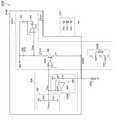
図8は、実施例に係る車両用灯具300Aのブロック図である。定電流ドライバ410Aは、電流源420Aおよび基準電圧生成回路430を備える。点灯回路400Aの主要部は、ひとつの半導体チップに集積化されている。
図8は、実施例に係る車両用灯具300Aのブロック図である。定電流ドライバ410Aは、電流源420Aおよび基準電圧生成回路430を備える。点灯回路400Aの主要部は、ひとつの半導体チップに集積化されている。
基準電圧生成回路430は、正常範囲において実質的に一定であり、第3温度T3より高い高温範囲において、温度Tとともに低下する基準電圧VREFを生成する。
点灯回路400Aには、電流設定端子(電流設定ピン)RSETが設けられる。電流設定端子RSETには、外付けの回路部品が接続可能となっている。電流源420Aは、基準電圧VREFに比例し、電流設定端子に接続される温度検出回路444のインピーダンス(抵抗値)RSETに反比例する駆動電流ILEDを生成する。
ILED∝VREF/RSET
ILED∝VREF/RSET
たとえば温度検出回路444は、電流設定端子RSETと接地間に直列に設けられた第1抵抗R21および第2抵抗R22と、第2抵抗R22と並列に設けられたNTC(負温度係数)サーミスタである第2サーミスタ402bと、を含んでもよい。
オペアンプ442、第2トランジスタQ2および温度検出回路444は、V/I変換回路を構成しており、その出力電流IREFは、
IREF=VREF/RSET
となる。I/V変換回路450は、基準電流IREFを調光電圧VDIMに変換する。
IREF=VREF/RSET
となる。I/V変換回路450は、基準電流IREFを調光電圧VDIMに変換する。
基準電圧生成回路430は、分圧回路432およびクランプ回路434を含む。分圧回路432は電源電圧Vccを分圧し、基準電圧VREFを発生する。クランプ回路434は、基準電圧VREFを、温度Tに応じた上限電圧以下にクランプする。クランプ回路434を無視したときの基準電圧VREF0は、以下の式で表される。
VREF0=VCC×R51/(R51+R52)
VREF0=VCC×R51/(R51+R52)
クランプ回路434は、第1トランジスタQ1、第1抵抗R1、第1サーミスタ402aを含む。第1トランジスタQ1はPNP型バイポーラトランジスタであり、分圧回路432の出力ノードと接地の間に設けられる。第1抵抗R1および温感素子402は、第2温度検出部であり、高温範囲において半導体光源302の温度に応じて有意に変化する第1検出信号Vaを生成し、温度に応じて第1トランジスタQ1の制御端子(ベース)をバイアスする。第1トランジスタQ1としてPチャンネルMOSFETを用いてもよい。あるいは第1トランジスタQ1に代えて、アノードに基準電圧VREFを受け、カソードに第1検出信号Vaを受けるダイオードを設けてもよい。
第1サーミスタ402aは、主として高温範囲における駆動電流ILEDの傾きを決定づける。第1サーミスタ402aの抵抗値Raは、負の温度係数(NTC:Negative Temperature Coefficient)を有している。第1抵抗R1と第1サーミスタ402aの接続ノードの電圧をVaとするとき、基準電圧VREFは、Va+Vfを上限としてクランプされる。
温度Tが正常範囲(T<T3)であるとき、Va+Vf>VREF0が成り立ち、したがってVREF=VREF0となり、温度に依存しない一定値となる。
温度Tが第3温度T3を超えて高温範囲に入るとVa+Vf<VREF0となり、クランプが有効となり、VREF=Va+Vfとなる。つまり温度が上昇するほどVaが低下し、したがって基準電圧VREFも低下する。
I/V変換回路450は、第3抵抗R3を含む。第3抵抗R3は、基準電流IREFの経路上に設けられる。調光電圧VDIMは、第3抵抗R3の電圧降下に応じている。
VDIM=VBAT-R3×IREF
VDIM=VBAT-R3×IREF
電流源420Aは、ソース型であり、抵抗R4、トランジスタM4、オペアンプ412を含み、調光電圧VDIMに比例した駆動電流ILEDを生成する。
ILED=IREF×R3/R4
ILED=IREF×R3/R4
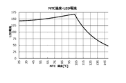
図9は、図8の定電流ドライバ410Aにおける駆動電流ILEDの温度特性を示す図である。この温度特性は、T0=25℃、T1=50℃、T2=80℃として設計したものであり、25~50℃の温度範囲における傾きよりも、50~80℃の温度範囲における傾きの方が大きくなっている。
実施例によれば、半導体光源の光束の安定性と信頼性を両立できる。
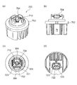
図10(a)~(d)は、車両用灯具300の一例であるLEDソケット700を示す図である。図10(a)はLEDソケット700の外観の斜視図である。図10(b)はLEDソケット700の正面図を、図10(c)はLEDソケット700の平面図を、図10(c)はLEDソケット700の底面図を示す。
筐体702は、図示しないランプボディに着脱可能な形状を有する。中央部には、半導体光源302を構成する複数の発光素子304が実装され、それらは透明のカバー704で覆われている。基板710には、点灯回路600の部品が実装される。複数の発光素子304は赤色のLEDチップであり、ストップランプやリアフォグランプとして利用される。
ストップランプとテールランプの兼用のLEDソケットでは、複数の発光素子304の中央に、テールランプ用の発光素子が実装され、基板710上には、テールランプ用の点灯回路が実装される。
筐体702の底面側には、3本のピン721、722、723が露出している。ピン723には、スイッチを介して第1入力電圧VIN1が供給され、ピン721には接地電圧が供給される。ピン722は、テールランプの点灯時にハイとなる第2入力電圧VIN2が供給される。ピン721~723は、筐体702の内部を貫通しており、それらの一端は、基板710の配線パターンと接続される。
実施の形態にもとづき、具体的な語句を用いて本発明を説明したが、実施の形態は、本発明の原理、応用を示しているにすぎず、実施の形態には、請求の範囲に規定された本発明の思想を逸脱しない範囲において、多くの変形例や配置の変更が認められる。
(変形例1)
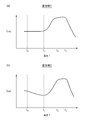
駆動電流ILEDの温度特性は、図4の例に限定されない。図11(a)は、変形例1に係る駆動電流ILEDの温度特性を示す図である。変形例1では、第1温度範囲T0~T1において、駆動電流ILEDがフラットであり、その傾きが非常に小さくなっている。
駆動電流ILEDの温度特性は、図4の例に限定されない。図11(a)は、変形例1に係る駆動電流ILEDの温度特性を示す図である。変形例1では、第1温度範囲T0~T1において、駆動電流ILEDがフラットであり、その傾きが非常に小さくなっている。
(変形例2)
図11(b)は、変形例2に係る駆動電流ILEDの温度特性を示す図である。変形例2では、第1温度範囲T0~T1において、駆動電流ILEDが温度増加にともなって減少し、したがって微分値は、負を採り得る。この場合、温度がT1に達する安定期間の開始時刻における光束をさらに下げることができ、安定期間の光束維持率を改善できる。
図11(b)は、変形例2に係る駆動電流ILEDの温度特性を示す図である。変形例2では、第1温度範囲T0~T1において、駆動電流ILEDが温度増加にともなって減少し、したがって微分値は、負を採り得る。この場合、温度がT1に達する安定期間の開始時刻における光束をさらに下げることができ、安定期間の光束維持率を改善できる。
(変形例3)
図12は、変形例3に係る定電流ドライバ410Bの回路図である。クランプ回路434Bは、図8の第1トランジスタQ1に代えて、オペアンプOA1およびダイオードD1を含む電流吸い込み(シンク)型のバッファ436を含む。バッファ436は、分圧回路432の出力ノードの電圧VREFを、Vaを超えないようにクランプする。図8の構成では、クランプレベルが、バイポーラトランジスタQ1のベースエミッタ間電圧Vfのバラツキの影響を受けるが、図12では、クランプレベルはダイオードD1の順方向電圧Vfの影響を受けないため、高精度である。
図12は、変形例3に係る定電流ドライバ410Bの回路図である。クランプ回路434Bは、図8の第1トランジスタQ1に代えて、オペアンプOA1およびダイオードD1を含む電流吸い込み(シンク)型のバッファ436を含む。バッファ436は、分圧回路432の出力ノードの電圧VREFを、Vaを超えないようにクランプする。図8の構成では、クランプレベルが、バイポーラトランジスタQ1のベースエミッタ間電圧Vfのバラツキの影響を受けるが、図12では、クランプレベルはダイオードD1の順方向電圧Vfの影響を受けないため、高精度である。
(変形例4)
定電流ドライバ410の構成は、実施例で説明したそれらに限定されず、公知のその他の回路構成を採用することができる。たとえば、定電流ドライバ410を、定電流出力のスイッチングコンバータで構成してもよい。スイッチングコンバータは、降圧型であってもよいし、昇圧型であってもよいし、昇降圧型であってもよく、その形式は、半導体光源302に含まれるダイオードの個数に応じて選択すればよい。
定電流ドライバ410の構成は、実施例で説明したそれらに限定されず、公知のその他の回路構成を採用することができる。たとえば、定電流ドライバ410を、定電流出力のスイッチングコンバータで構成してもよい。スイッチングコンバータは、降圧型であってもよいし、昇圧型であってもよいし、昇降圧型であってもよく、その形式は、半導体光源302に含まれるダイオードの個数に応じて選択すればよい。
(変形例5)
実施の形態では、温感素子として負の温度係数を有するNTCサーミスタを用いたがその限りでなく、PTCサーミスタ(ポジスタ)を用いてもよい。あるいは、PN接合(すなわちダイオード)に定電流を流したときの両端間電圧が、温度依存性を有することを利用したダイオード温度センサを温感素子として用いてもよい。
実施の形態では、温感素子として負の温度係数を有するNTCサーミスタを用いたがその限りでなく、PTCサーミスタ(ポジスタ)を用いてもよい。あるいは、PN接合(すなわちダイオード)に定電流を流したときの両端間電圧が、温度依存性を有することを利用したダイオード温度センサを温感素子として用いてもよい。
(変形例6)
また、実施例では、アナログ回路によって、駆動電流の温度特性を設計したが、その限りでない。たとえば温感素子の出力をデジタル値に変換し、デジタル制御によって、駆動電流ILEDの温度特性を作るようにしてもよい。
また、実施例では、アナログ回路によって、駆動電流の温度特性を設計したが、その限りでない。たとえば温感素子の出力をデジタル値に変換し、デジタル制御によって、駆動電流ILEDの温度特性を作るようにしてもよい。
(変形例7)
実施の形態では、調光電圧VDIMにもとづくアナログ調光(リニア調光)により、駆動電流ILEDを変化させたがその限りでなく、PWM調光を用いてもよい。この場合、調光電圧VDIMに応じたデューティ比を有する調光パルスを生成し、調光パルスにもとづいて、一定量に安定化された定電流をスイッチングすることにより駆動電流ILEDを生成してもよい。
実施の形態では、調光電圧VDIMにもとづくアナログ調光(リニア調光)により、駆動電流ILEDを変化させたがその限りでなく、PWM調光を用いてもよい。この場合、調光電圧VDIMに応じたデューティ比を有する調光パルスを生成し、調光パルスにもとづいて、一定量に安定化された定電流をスイッチングすることにより駆動電流ILEDを生成してもよい。
(変形例8)
アナログ調光とPWM調光を組み合わせてもよい。たとえば高温範囲の温度ディレーティングを、アナログ調光で行い、正常範囲の輝度の安定化をPWM調光で行ってもよい。あるいはそれらの逆であってもよい。
アナログ調光とPWM調光を組み合わせてもよい。たとえば高温範囲の温度ディレーティングを、アナログ調光で行い、正常範囲の輝度の安定化をPWM調光で行ってもよい。あるいはそれらの逆であってもよい。
(変形例9)
温度上昇にともなう光束の低下は、赤色のLEDにおいて特に顕著であるが、他の色のLEDやLD(レーザダイオード)にも、同様の特性を有するものがある。したがって、本開示は、さまざまな半導体光源を備える車両用灯具において有用である。
温度上昇にともなう光束の低下は、赤色のLEDにおいて特に顕著であるが、他の色のLEDやLD(レーザダイオード)にも、同様の特性を有するものがある。したがって、本開示は、さまざまな半導体光源を備える車両用灯具において有用である。
本開示は、自動車などの灯具に利用できる。
300…車両用灯具,302…半導体光源,400…点灯回路,402…温感素子,402a…第1サーミスタ,402b…第2サーミスタ,410…定電流ドライバ,420…電流源,430…基準電圧生成回路,432…分圧回路,434…クランプ回路,Q1…第1トランジスタ,R1…第1抵抗,444…温度検出回路,Q2…第2トランジスタ,R2…第2抵抗,442…オペアンプ,450…I/V変換回路,VDIM…調光電圧。
Claims (8)
- 半導体光源の温度Tに応じて電気的状態が変化する温感素子と、
前記温度Tに応じた駆動電流を生成する定電流ドライバと、
を備え、
基準温度T0から第1温度T1(T1>T0)までの第1温度範囲T0~T1における前記駆動電流の温度微分の最大値は、前記第1温度T1から第2温度T2(T2>T1)までの第2温度範囲T1~T2における前記駆動電流の温度微分の最大値よりも小さいことを特徴とする点灯回路。 - 前記第1温度T1は、安定期間の開始時刻の温度にもとづいて定められ、
前記第2温度T2は、安定期間の定常的な温度にもとづいて定められることを特徴とする請求項1に記載の点灯回路。 - 前記第1温度範囲T0~T1における前記駆動電流の温度微分と前記第2温度範囲T1~T2における前記駆動電流の温度微分は両方、正であることを特徴とする請求項1または2に記載の点灯回路。
- 前記第1温度範囲T0~T1において前記駆動電流の温度微分は負をとり、前記第2温度範囲T1~T2において前記駆動電流の温度微分は正であることを特徴とする請求項1または2に記載の点灯回路。
- 第3温度T3(T3>T2)より高い第3範囲において、前記駆動電流は減少することを特徴とする請求項1から4のいずれかに記載の点灯回路。
- 前記定電流ドライバは、
電流設定端子を有し、前記電流設定端子に接続される回路のインピーダンスに反比例する前記駆動電流を生成する電流源と、
前記電流設定端子と接地間に直列に設けられた第1抵抗および第2抵抗と、
前記第2抵抗と並列に設けられたNTC(負温度係数)サーミスタと、
を含むことを特徴とする請求項1から3のいずれかに記載の点灯回路。 - 半導体光源と、
前記半導体光源を駆動する請求項1から5のいずれかに記載の点灯回路と、
を備えることを特徴とする車両用灯具。 - 半導体光源と、
前記半導体光源に駆動電流を供給する点灯回路と、
を備え、
点灯開始直後のスタート期間の駆動電流の変化量は、スタート期間に続く安定期間の駆動電流の増加量よりも小さいことを特徴とする車両用灯具。
Priority Applications (4)
| Application Number | Priority Date | Filing Date | Title |
|---|---|---|---|
| CN202180010164.0A CN115210110A (zh) | 2020-01-20 | 2021-01-13 | 点亮电路及车辆用灯具 |
| JP2021573089A JP7524229B2 (ja) | 2020-01-20 | 2021-01-13 | 点灯回路および車両用灯具 |
| EP21744518.8A EP4094987A4 (en) | 2020-01-20 | 2021-01-13 | IGNITION SYSTEM AND VEHICLE HEADLIGHT |
| US17/867,870 US12048073B2 (en) | 2020-01-20 | 2022-07-19 | Lighting circuit |
Applications Claiming Priority (2)
| Application Number | Priority Date | Filing Date | Title |
|---|---|---|---|
| JP2020006923 | 2020-01-20 | ||
| JP2020-006923 | 2020-01-20 |
Related Child Applications (1)
| Application Number | Title | Priority Date | Filing Date |
|---|---|---|---|
| US17/867,870 Continuation US12048073B2 (en) | 2020-01-20 | 2022-07-19 | Lighting circuit |
Publications (1)
| Publication Number | Publication Date |
|---|---|
| WO2021149558A1 true WO2021149558A1 (ja) | 2021-07-29 |
Family
ID=76992571
Family Applications (1)
| Application Number | Title | Priority Date | Filing Date |
|---|---|---|---|
| PCT/JP2021/000853 Ceased WO2021149558A1 (ja) | 2020-01-20 | 2021-01-13 | 点灯回路および車両用灯具 |
Country Status (5)
| Country | Link |
|---|---|
| US (1) | US12048073B2 (ja) |
| EP (1) | EP4094987A4 (ja) |
| JP (1) | JP7524229B2 (ja) |
| CN (1) | CN115210110A (ja) |
| WO (1) | WO2021149558A1 (ja) |
Families Citing this family (1)
| Publication number | Priority date | Publication date | Assignee | Title |
|---|---|---|---|---|
| WO2022194582A1 (de) * | 2021-03-16 | 2022-09-22 | HELLA GmbH & Co. KGaA | Lichtkörper für eine leuchte eines fahrzeuges, leuchte eines fahrzeuges sowie verfahren zum einstellen eines elektrischen stromes einer lichtquelle eines lichtkörpers |
Citations (3)
| Publication number | Priority date | Publication date | Assignee | Title |
|---|---|---|---|---|
| WO2016158423A1 (ja) | 2015-03-31 | 2016-10-06 | 株式会社小糸製作所 | 光源ユニット及び車輌用灯具 |
| JP2019169655A (ja) * | 2018-03-26 | 2019-10-03 | ローム株式会社 | 発光素子駆動装置 |
| WO2020013032A1 (ja) * | 2018-07-13 | 2020-01-16 | 株式会社小糸製作所 | 点灯回路および車両用灯具 |
Family Cites Families (12)
| Publication number | Priority date | Publication date | Assignee | Title |
|---|---|---|---|---|
| JP5230004B2 (ja) * | 2008-11-14 | 2013-07-10 | 株式会社小糸製作所 | 車両用灯具の点灯制御装置 |
| KR101801681B1 (ko) * | 2009-05-08 | 2017-11-27 | 필립스 라이팅 홀딩 비.브이. | 광 특성 감지 회로 및 방법 |
| DE102010006998A1 (de) * | 2010-02-05 | 2011-08-11 | Siteco Beleuchtungstechnik GmbH, 83301 | Temperaturkompensation des Lichtstroms an LED-Leuchten |
| US9408278B2 (en) * | 2012-02-07 | 2016-08-02 | Panasonic Intellectual Property Management Co., Ltd. | Light-emitting circuit with variable resistor element, and light-emitting module and illumination device including the same |
| JP6278298B2 (ja) * | 2013-09-10 | 2018-02-14 | パナソニックIpマネジメント株式会社 | 点灯装置及びそれを用いた前照灯装置、並びに車両 |
| JP6131510B2 (ja) * | 2013-09-10 | 2017-05-24 | パナソニックIpマネジメント株式会社 | 点灯装置及びそれを用いた前照灯装置、並びに車両 |
| ITTV20130177A1 (it) * | 2013-10-24 | 2015-04-25 | Automotive Lighting Italia Spa | Fanale per autoveicoli provvisto di un dispositivo di illuminazione a led |
| CN104797060B (zh) * | 2015-05-13 | 2017-11-10 | 昂宝电子(上海)有限公司 | 用于发光二极管照明系统中的温度控制的系统和方法 |
| CN106851889B (zh) * | 2015-12-04 | 2018-11-23 | 法雷奥照明湖北技术中心有限公司 | 用于发光二极管的温度自适应控制电路及照明和/或信号指示装置 |
| JP6820909B2 (ja) * | 2016-03-03 | 2021-01-27 | 株式会社小糸製作所 | 車両用灯具およびその点灯回路 |
| EP3474632B1 (de) * | 2017-10-19 | 2020-07-15 | ZKW Group GmbH | Schaltungsanordnung zum erzeugen einer referenzspannung für die stromversorgung einer led-anordnung |
| FR3085099B1 (fr) * | 2018-06-22 | 2023-06-30 | Valeo Vision | Dispositif de pilotage de l'alimentation electrique de sources lumineuses d'un vehicule automobile en fonction des variations de leurs temperatures |
-
2021
- 2021-01-13 JP JP2021573089A patent/JP7524229B2/ja active Active
- 2021-01-13 EP EP21744518.8A patent/EP4094987A4/en not_active Withdrawn
- 2021-01-13 WO PCT/JP2021/000853 patent/WO2021149558A1/ja not_active Ceased
- 2021-01-13 CN CN202180010164.0A patent/CN115210110A/zh active Pending
-
2022
- 2022-07-19 US US17/867,870 patent/US12048073B2/en active Active
Patent Citations (3)
| Publication number | Priority date | Publication date | Assignee | Title |
|---|---|---|---|---|
| WO2016158423A1 (ja) | 2015-03-31 | 2016-10-06 | 株式会社小糸製作所 | 光源ユニット及び車輌用灯具 |
| JP2019169655A (ja) * | 2018-03-26 | 2019-10-03 | ローム株式会社 | 発光素子駆動装置 |
| WO2020013032A1 (ja) * | 2018-07-13 | 2020-01-16 | 株式会社小糸製作所 | 点灯回路および車両用灯具 |
Non-Patent Citations (1)
| Title |
|---|
| See also references of EP4094987A4 |
Also Published As
| Publication number | Publication date |
|---|---|
| JPWO2021149558A1 (ja) | 2021-07-29 |
| US12048073B2 (en) | 2024-07-23 |
| JP7524229B2 (ja) | 2024-07-29 |
| EP4094987A1 (en) | 2022-11-30 |
| EP4094987A4 (en) | 2023-06-07 |
| US20220353966A1 (en) | 2022-11-03 |
| CN115210110A (zh) | 2022-10-18 |
Similar Documents
| Publication | Publication Date | Title |
|---|---|---|
| CN111955055B (zh) | 车辆用灯具及其点亮电路 | |
| JP5120537B2 (ja) | 照明装置 | |
| JP7182925B2 (ja) | 車両用灯具 | |
| JP2010129612A (ja) | 点灯装置 | |
| KR20080100225A (ko) | 온도 제어 led 어레이 | |
| US9137871B2 (en) | Method and circuit arrangement for producing mixed LED light of a predetermined color | |
| CN110626253B (zh) | 用于根据其温度变化来驱动机动车辆的光源的电源的装置 | |
| JP7614184B2 (ja) | 車両用灯具および点灯回路 | |
| JP7353358B2 (ja) | 車両用灯具およびその点灯回路 | |
| CN105432143B (zh) | 照明装置和包括所述照明装置的汽车车灯 | |
| JP2009302296A (ja) | 発光ダイオード駆動装置並びにそれを用いた照明器具、車室内用照明装置、車両用照明装置 | |
| US11197356B2 (en) | Lighting circuit and vehicle lamp | |
| JP7018124B2 (ja) | 発光素子駆動装置 | |
| JP7524229B2 (ja) | 点灯回路および車両用灯具 | |
| CN114207348A (zh) | 光源模块 | |
| WO2022202670A1 (ja) | 発光素子駆動装置、発光装置、および車両 | |
| US7368885B2 (en) | Lighting controller for lighting device for vehicle | |
| JP2017021970A (ja) | 点灯装置、照明装置及びそれを用いた車両 | |
| JP2009214789A (ja) | 車両用灯具 | |
| US10917949B2 (en) | Light module for a motor vehicle comprising a plurality of light source branches | |
| US20090309517A1 (en) | Temperature dependent current control circuit for LED lighting | |
| US20230397312A1 (en) | Light arrangement | |
| CN221177971U (zh) | 色温调控灯具 | |
| JP6964256B2 (ja) | 照明装置、および照明器具 | |
| JP2024062291A (ja) | 点灯回路および車両用灯具 |
Legal Events
| Date | Code | Title | Description |
|---|---|---|---|
| 121 | Ep: the epo has been informed by wipo that ep was designated in this application |
Ref document number: 21744518 Country of ref document: EP Kind code of ref document: A1 |
|
| ENP | Entry into the national phase |
Ref document number: 2021573089 Country of ref document: JP Kind code of ref document: A |
|
| NENP | Non-entry into the national phase |
Ref country code: DE |
|
| ENP | Entry into the national phase |
Ref document number: 2021744518 Country of ref document: EP Effective date: 20220822 |