WO2021166979A1 - 撮像素子及び撮像装置 - Google Patents
撮像素子及び撮像装置 Download PDFInfo
- Publication number
- WO2021166979A1 WO2021166979A1 PCT/JP2021/006011 JP2021006011W WO2021166979A1 WO 2021166979 A1 WO2021166979 A1 WO 2021166979A1 JP 2021006011 W JP2021006011 W JP 2021006011W WO 2021166979 A1 WO2021166979 A1 WO 2021166979A1
- Authority
- WO
- WIPO (PCT)
- Prior art keywords
- unit
- pixel
- control block
- control
- block
- Prior art date
- Legal status (The legal status is an assumption and is not a legal conclusion. Google has not performed a legal analysis and makes no representation as to the accuracy of the status listed.)
- Ceased
Links
Images


Classifications
-
- H—ELECTRICITY
- H04—ELECTRIC COMMUNICATION TECHNIQUE
- H04N—PICTORIAL COMMUNICATION, e.g. TELEVISION
- H04N25/00—Circuitry of solid-state image sensors [SSIS]; Control thereof
- H04N25/50—Control of the SSIS exposure
- H04N25/57—Control of the dynamic range
- H04N25/58—Control of the dynamic range involving two or more exposures
-
- H—ELECTRICITY
- H04—ELECTRIC COMMUNICATION TECHNIQUE
- H04N—PICTORIAL COMMUNICATION, e.g. TELEVISION
- H04N25/00—Circuitry of solid-state image sensors [SSIS]; Control thereof
- H04N25/50—Control of the SSIS exposure
-
- H—ELECTRICITY
- H04—ELECTRIC COMMUNICATION TECHNIQUE
- H04N—PICTORIAL COMMUNICATION, e.g. TELEVISION
- H04N25/00—Circuitry of solid-state image sensors [SSIS]; Control thereof
- H04N25/50—Control of the SSIS exposure
- H04N25/53—Control of the integration time
- H04N25/533—Control of the integration time by using differing integration times for different sensor regions
- H04N25/535—Control of the integration time by using differing integration times for different sensor regions by dynamic region selection
-
- H—ELECTRICITY
- H04—ELECTRIC COMMUNICATION TECHNIQUE
- H04N—PICTORIAL COMMUNICATION, e.g. TELEVISION
- H04N25/00—Circuitry of solid-state image sensors [SSIS]; Control thereof
- H04N25/70—SSIS architectures; Circuits associated therewith
- H04N25/71—Charge-coupled device [CCD] sensors; Charge-transfer registers specially adapted for CCD sensors
- H04N25/74—Circuitry for scanning or addressing the pixel array
-
- H—ELECTRICITY
- H04—ELECTRIC COMMUNICATION TECHNIQUE
- H04N—PICTORIAL COMMUNICATION, e.g. TELEVISION
- H04N25/00—Circuitry of solid-state image sensors [SSIS]; Control thereof
- H04N25/70—SSIS architectures; Circuits associated therewith
- H04N25/71—Charge-coupled device [CCD] sensors; Charge-transfer registers specially adapted for CCD sensors
- H04N25/75—Circuitry for providing, modifying or processing image signals from the pixel array
-
- H—ELECTRICITY
- H04—ELECTRIC COMMUNICATION TECHNIQUE
- H04N—PICTORIAL COMMUNICATION, e.g. TELEVISION
- H04N25/00—Circuitry of solid-state image sensors [SSIS]; Control thereof
- H04N25/70—SSIS architectures; Circuits associated therewith
- H04N25/76—Addressed sensors, e.g. MOS or CMOS sensors
- H04N25/77—Pixel circuitry, e.g. memories, A/D converters, pixel amplifiers, shared circuits or shared components
- H04N25/771—Pixel circuitry, e.g. memories, A/D converters, pixel amplifiers, shared circuits or shared components comprising storage means other than floating diffusion
-
- H—ELECTRICITY
- H04—ELECTRIC COMMUNICATION TECHNIQUE
- H04N—PICTORIAL COMMUNICATION, e.g. TELEVISION
- H04N25/00—Circuitry of solid-state image sensors [SSIS]; Control thereof
- H04N25/70—SSIS architectures; Circuits associated therewith
- H04N25/76—Addressed sensors, e.g. MOS or CMOS sensors
- H04N25/78—Readout circuits for addressed sensors, e.g. output amplifiers or A/D converters
-
- H—ELECTRICITY
- H04—ELECTRIC COMMUNICATION TECHNIQUE
- H04N—PICTORIAL COMMUNICATION, e.g. TELEVISION
- H04N25/00—Circuitry of solid-state image sensors [SSIS]; Control thereof
- H04N25/70—SSIS architectures; Circuits associated therewith
- H04N25/79—Arrangements of circuitry being divided between different or multiple substrates, chips or circuit boards, e.g. stacked image sensors
-
- H—ELECTRICITY
- H10—SEMICONDUCTOR DEVICES; ELECTRIC SOLID-STATE DEVICES NOT OTHERWISE PROVIDED FOR
- H10F—INORGANIC SEMICONDUCTOR DEVICES SENSITIVE TO INFRARED RADIATION, LIGHT, ELECTROMAGNETIC RADIATION OF SHORTER WAVELENGTH OR CORPUSCULAR RADIATION
- H10F39/00—Integrated devices, or assemblies of multiple devices, comprising at least one element covered by group H10F30/00, e.g. radiation detectors comprising photodiode arrays
- H10F39/80—Constructional details of image sensors
- H10F39/802—Geometry or disposition of elements in pixels, e.g. address-lines or gate electrodes
-
- H—ELECTRICITY
- H10—SEMICONDUCTOR DEVICES; ELECTRIC SOLID-STATE DEVICES NOT OTHERWISE PROVIDED FOR
- H10F—INORGANIC SEMICONDUCTOR DEVICES SENSITIVE TO INFRARED RADIATION, LIGHT, ELECTROMAGNETIC RADIATION OF SHORTER WAVELENGTH OR CORPUSCULAR RADIATION
- H10F39/00—Integrated devices, or assemblies of multiple devices, comprising at least one element covered by group H10F30/00, e.g. radiation detectors comprising photodiode arrays
- H10F39/80—Constructional details of image sensors
- H10F39/803—Pixels having integrated switching, control, storage or amplification elements
-
- H—ELECTRICITY
- H10—SEMICONDUCTOR DEVICES; ELECTRIC SOLID-STATE DEVICES NOT OTHERWISE PROVIDED FOR
- H10F—INORGANIC SEMICONDUCTOR DEVICES SENSITIVE TO INFRARED RADIATION, LIGHT, ELECTROMAGNETIC RADIATION OF SHORTER WAVELENGTH OR CORPUSCULAR RADIATION
- H10F39/00—Integrated devices, or assemblies of multiple devices, comprising at least one element covered by group H10F30/00, e.g. radiation detectors comprising photodiode arrays
- H10F39/80—Constructional details of image sensors
- H10F39/809—Constructional details of image sensors of hybrid image sensors
-
- H—ELECTRICITY
- H04—ELECTRIC COMMUNICATION TECHNIQUE
- H04N—PICTORIAL COMMUNICATION, e.g. TELEVISION
- H04N25/00—Circuitry of solid-state image sensors [SSIS]; Control thereof
- H04N25/70—SSIS architectures; Circuits associated therewith
- H04N25/76—Addressed sensors, e.g. MOS or CMOS sensors
- H04N25/766—Addressed sensors, e.g. MOS or CMOS sensors comprising control or output lines used for a plurality of functions, e.g. for pixel output, driving, reset or power
Definitions
- the present invention relates to an image pickup device and an image pickup device.
- Patent Document 1 International Publication No. 2017/018188
- a signal from a pixel chip having a plurality of pixel blocks including one or a plurality of pixels and a pixel included in at least the first pixel block among the plurality of pixel blocks is converted into a digital signal.
- a first control block including a first conversion unit and a first storage unit that stores a digital signal converted by the first conversion unit, and a plurality of pixel blocks arranged next to the first control block in the column direction.
- a second control block including at least a second conversion unit that converts a signal from a pixel included in the second pixel block into a digital signal and a second storage unit that stores a digital signal converted by the second conversion unit.
- the second conversion unit and the second storage unit in the second control block are vertically inverted positions with respect to the arrangement positions of the first conversion unit and the first storage unit in the first control block.
- an image pickup element arranged in.
- an image pickup device including the image pickup device of the first aspect is provided.
- FIG. 400 It is a figure which shows the outline of the image pickup device 400 which concerns on embodiment of this invention.
- An example of a specific configuration of the pixel unit 110 is shown.
- An example of the circuit configuration of the pixel 112 is shown.
- An example of a more specific configuration of the main circuit unit 210 is shown.
- An example of a specific configuration of the control block 220 is shown.
- An example of a plurality of control blocks 220 according to an embodiment is shown.
- An example of the arrangement method of the control block 720 according to the comparative example is shown.
- An example of the configuration of the image sensor 400 is shown.
- An example of the configuration of the image pickup device 800 according to the comparative example is shown. It is a figure for demonstrating an example of the wiring method of the image sensor 400.
- FIG. 8A An example of the configuration of the pixel unit 610 according to the comparative example is shown.
- An example of the configuration of the main circuit unit 710 according to the comparative example is shown.
- An example of the configuration of the main circuit unit 710 according to the comparative example is shown.
- An example of the configuration of the main circuit unit 710 according to the comparative example is shown.
- An example of a timing chart showing the image pickup operation of the image pickup device 400 is shown. An example of the exposure timing for each pixel group 115 is shown.
- An example of the configuration of the signal processing chip 200 is shown.
- An example of the cross-sectional view of the signal processing chip 200 is shown.
- An example of the configuration of the signal processing chip 700 according to the comparative example is shown.
- Another example of the signal processing chip 700 according to the comparative example is shown.
- An example of the cross-sectional view of the signal processing chip 700 according to the comparative example is shown. It is a block diagram which shows the structural example of the image pickup apparatus 500 which concerns on Example.
- the X-axis and the Y-axis are orthogonal to each other, and the Z-axis is orthogonal to the XY plane.
- the XYZ axes constitute a right-handed system.
- the direction parallel to the Z axis may be referred to as the stacking direction of the image sensor 400.
- the terms "up” and “down” are not limited to the up and down directions in the direction of gravity. These terms only refer to the relative direction in the Z-axis direction.
- the arrangement in the X-axis direction is referred to as a "row” and the arrangement in the Y-axis direction is referred to as a "column", but the matrix direction is not limited to this.
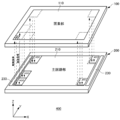
- FIG. 1A is a diagram showing an outline of the image pickup device 400 according to the present embodiment.
- the image sensor 400 captures a subject.
- the image sensor 400 generates image data of the captured subject.
- the image sensor 400 includes a pixel chip 100 and a signal processing chip 200. As shown in FIG. 1A, the pixel chip 100 is stacked on the signal processing chip 200.
- the pixel chip 100 has a pixel unit 110.
- the pixel unit 110 outputs a pixel signal based on the incident light.
- the signal processing chip 200 has a main circuit unit 210 and a peripheral circuit unit 230.
- the pixel signal output from the pixel chip 100 is input to the main circuit unit 210.
- the main circuit unit 210 processes the input pixel signal.
- the main circuit unit 210 of this example is arranged at a position facing the pixel unit 110 in the signal processing chip 200.
- the main circuit unit 210 may output a control signal for controlling the drive of the pixel unit 110 to the pixel unit 110.
- the peripheral circuit unit 230 controls the drive of the main circuit unit 210.
- the peripheral circuit unit 230 is arranged around the main circuit unit 210 in the signal processing chip 200. Further, the peripheral circuit unit 230 may be electrically connected to the pixel chip 100 to control the drive of the pixel unit 110.
- the peripheral circuit unit 230 of this example is arranged along two sides of the signal processing chip 200, but the method of arranging the peripheral circuit unit 230 is not limited to this example.
- the image sensor 400 may have a memory chip laminated on the signal processing chip 200 in addition to the pixel chip 100 and the signal processing chip 200.
- the memory chip performs image processing according to the signal output by the signal processing chip 200.
- the structure of the image sensor 400 may be a back-illuminated type or a front-illuminated type.
- FIG. 1B shows an example of a specific configuration of the pixel unit 110.
- an enlarged view of the pixel unit 110 and the pixel block 120 provided in the pixel unit 110 is shown.
- the pixel unit 110 has a plurality of pixel groups 115 arranged side by side along the row direction and the column direction.
- the pixel unit 110 of this example has M ⁇ N (M and N are natural numbers) pixel group 115. In this example, the case where M is equal to N is shown, but M and N may be different.
- the pixel group 115 has at least one pixel 112.
- the pixel group 115 of this example has m ⁇ n (m and n are natural numbers) pixels 112.
- the pixel group 115 has 16 ⁇ 16 pixels 112.
- the number of pixels 112 corresponding to the pixel group 115 is not limited to this. In this example, the case where m is equal to n is shown, but m may be different from n.
- the pixel group 115 has a plurality of pixels 112 connected to a common control line in the row direction.
- each pixel 112 of the pixel group 115 is connected to a common control line so as to be set to the same exposure time.
- n pixels 112 arranged in the row direction are connected by a common control line.
- the pixel group 115 may be set to different exposure times. That is, each pixel 112 of the pixel group 115 has the same exposure time, but the other pixel groups 115 may be set to different exposure times. For example, when the pixels 112 of the pixel group 115 are connected by a common control line in the row direction, the pixels 112 of the other pixel group 115 are commonly connected by different control lines.
- the pixel block 120 has one or more pixel groups 115.
- the pixel block 120 of this example has two pixel groups 115 arranged side by side along the column direction.
- the pixel block 120 is arranged corresponding to the control block 220 described later. That is, two pixel groups 115 are arranged for one control block 220.
- each pixel group 115 may be set to a different exposure time.
- one pixel group 115 is arranged with respect to the control block 220.
- the pixel block 120 has 2 m ⁇ n pixels 112.
- the pixel block 120 has 32 ⁇ 16 pixels 112.
- the number of pixels 112 corresponding to the pixel block 120 is not limited to this.
- Pixel 112 has a photoelectric conversion function that converts light into electric charges. Pixels 112 store photoelectrically converted charges.
- the 2 m pixels 112 are arranged along the column direction and are connected to a common signal line 122. The 2 m pixels 112 are arranged in n columns in the row direction in the pixel block 120.
- FIG. 1C shows an example of the circuit configuration of the pixel 112.
- the pixel 112 includes a photoelectric conversion unit 104, a first transfer unit 123, a second transfer unit 124, a reset unit 126, and a pixel output unit 127.
- the pixel output unit 127 includes an amplification unit 128 and a selection unit 129.
- the first transfer unit 123, the second transfer unit 124, the reset unit 126, the amplification unit 128, and the selection unit 129 are described as N-channel FETs, but the type of transistor is not limited to this.
- the photoelectric conversion unit 104 has a photoelectric conversion function that converts light into electric charges.
- the photoelectric conversion unit 104 accumulates the photoelectrically converted charges.
- the photoelectric conversion unit 104 is, for example, a photodiode.
- the first transfer unit 123 transfers the electric charge accumulated in the photoelectric conversion unit 104 to the storage unit 125.
- the first transfer unit 123 is an example of a transfer gate that transfers the electric charge of the photoelectric conversion unit 104.
- the gate terminal of the first transfer unit 123 is connected to a local control line for inputting the first transfer control signal ⁇ TX1.
- the local control line will be described later.
- the second transfer unit 124 discharges the electric charge accumulated in the photoelectric conversion unit 104 to the power supply wiring to which the power supply voltage VDD is supplied.
- the gate terminal of the second transfer unit 124 is connected to a local control line for inputting the second transfer control signal ⁇ TX2.
- the second transfer unit 124 has been described as discharging the electric charge of the photoelectric conversion unit 104 to the power supply wiring to which the power supply voltage VDD is supplied, but the power supply is supplied with a power supply voltage different from the power supply voltage VDD. It may be discharged to the wiring.
- the electric charge from the photoelectric conversion unit 104 is transferred to the storage unit 125 by the first transfer unit 123.
- the storage unit 125 is an example of a floating diffusion (FD).
- the reset unit 126 discharges the electric charge of the storage unit 125 to the power supply wiring to which the predetermined power supply voltage VDD is supplied.
- the gate terminal of the reset unit 126 is connected to the global control line 143 for inputting the reset control signal ⁇ RST.
- the global control line 143 will be described later.
- the pixel output unit 127 outputs a signal based on the potential of the storage unit 125 to the signal line 122.
- the pixel output unit 127 includes an amplification unit 128 and a selection unit 129.
- the gate terminal is connected to the storage unit 125
- the drain terminal is connected to the power supply wiring to which the power supply voltage VDD is supplied
- the source terminal is connected to the drain terminal of the selection unit 129.
- the selection unit 129 controls the electrical connection between the pixel 112 and the signal line 122.
- a pixel signal is output from the pixel 112 to the signal line 122.
- the gate terminal of the selection unit 129 is connected to the global control line 143 for inputting the selection control signal ⁇ SEL.
- the source terminal of the selection unit 129 is connected to the load current source 121.
- the load current source 121 supplies a current to the signal line 122.
- the load current source 121 may be provided on the pixel chip 100 or the signal processing chip 200.
- FIG. 1D shows an example of a more specific configuration of the main circuit unit 210.
- an enlarged view of the main circuit unit 210 and the control block 220 provided in the main circuit unit 210 is shown.
- the main circuit unit 210 has a control block 220 arranged along the row direction and the column direction.
- the main circuit unit 210 of this example has (M / 2) ⁇ N control blocks 220.
- the main circuit unit 210 has one control block 220 for two pixel groups 115 arranged side by side in the column direction.
- the control block 220 is arranged at a position corresponding to the pixel block 120, respectively.
- the control block 220 controls the drive of the corresponding pixel block 120.
- the control block 220 controls the exposure time of the pixel block 120.
- the control block 220 may control the exposure time for each pixel group 115.
- the control block 220 has a processing circuit such as an AD converter, and processes the signal output by the pixel block 120.
- the control block 220 converts an analog pixel signal output from the corresponding pixel block 120 into a digital signal.
- the control block 220 of this example includes an exposure control unit 10, a pixel drive unit 20, a joint unit 30, a signal conversion unit 40, and a signal output unit 50.
- the exposure control unit 10 controls the exposure of a plurality of pixels 112.
- the exposure control unit 10 generates a signal for controlling the exposure time of the pixel 112.
- the exposure control unit 10 adjusts at least one of the start timing and the end timing of the exposure to control the exposure time for each pixel group 115.
- the exposure control unit 10 of this example is provided so as to extend in the row direction.
- the pixel drive unit 20 is joined to the pixel chip 100 to drive a plurality of pixels 112.
- the pixel driving unit 20 selects and drives an arbitrary pixel 112 from a plurality of pixels 112.
- the pixel drive unit 20 of this example is provided so as to extend in the row direction.
- the pixel drive unit 20 is arranged at a position corresponding to the 2 m pixels 112 arranged in the row direction.
- the exposure control unit 10 and the pixel drive unit 20 are arranged in an L shape by the pixel drive unit 20 extending in the column direction and the exposure control unit 10 extending in the row direction.
- the joining portion 30 joins the pixel chip 100 and the signal processing chip 200.
- the joining portion 30 inputs the pixel signal input from the pixel chip 100 to the signal conversion unit 40.
- the joining portion 30 is provided corresponding to n pixels 112 arranged in the row direction, and a pixel signal is input to the signal conversion unit 40 for each column.
- the signal conversion unit 40 digitally converts the analog signal output by the pixel unit 110.
- the signal conversion unit 40 of this example converts an analog pixel signal into a digital signal.
- the signal conversion unit 40 sequentially digitally converts analog signals from 2 m pixels 112 arranged in the column direction.
- the signal conversion unit 40 digitally converts analog signals from pixels 112 arranged in n columns in the row direction in parallel.
- the signal output unit 50 receives a digital signal from the signal conversion unit 40.
- the signal output unit 50 temporarily stores a digital signal.
- the signal output unit 50 may have a latch circuit for storing a digital signal.
- the signal output unit 50 is provided between the signal conversion unit 40 and the exposure control unit 10 in the column direction, and outputs a digital signal.
- the signal output unit 50 of this example outputs a digital signal to the outside of the main circuit unit 210.
- the signal output unit 50 extends in the row direction and is provided adjacent to the signal conversion unit 40 and the exposure control unit 10.
- the image sensor 400 of this example has a function of reading pixel signals in parallel by a control block 220 provided for each pixel block 120. Since the image sensor 400 can set the exposure time for each pixel group 115 according to the intensity of the incident light, the dynamic range can be expanded.
- FIG. 2A shows an example of a specific configuration of the control block 220.
- the signal conversion unit 40 of this example includes n comparators 42 and a storage unit 44.
- the control block 220 of this example includes a local control unit 12 and a level shift unit 14 that constitute the exposure control unit 10.
- the comparator 42 is provided so as to extend in the column direction. The n comparators 42 are arranged in the row direction. One comparator 42 is provided for every 2 m of pixels 112. The comparator 42 sequentially reads the pixel signals of the 2 m pixels 112 and converts them into digital signals.
- the storage unit 44 temporarily stores the digital signal from the comparator 42.
- the storage unit 44 of this example is provided in the signal conversion unit 40 on the negative side in the Y-axis direction with respect to the comparator 42.
- the storage unit 44 has a latch circuit.
- the storage unit 44 may have a memory configured by SRAM or the like.
- the local control unit 12 outputs a control signal for controlling the operation of the first transfer unit 123 and the second transfer unit 124.
- the local control unit 12 locally controls either the first transfer control signal ⁇ TX1 or the second transfer control signal ⁇ TX2.
- the local control refers to controlling the drive for each pixel block 120.
- the local control unit 12 locally controls the second transfer control signal ⁇ TX2.
- the local control unit 12 is provided so as to extend in the row direction.
- the local control unit 12 is provided between the level shift unit 14 and the signal output unit 50.
- the level shift unit 14 converts the voltage level of the control signal output by the local control unit 12 and outputs it.
- the level shift portion 14 is provided so as to extend in the row direction.
- the level shift unit 14 is provided on the outer peripheral side of the control block 220 with respect to the local control unit 12.
- the end of the level shift portion 14 on the positive side in the X-axis direction and the end on the negative side in the Y-axis direction are located on the outermost side of the control block 220.
- the end of the level shift unit 14 on the negative side in the X-axis direction is in contact with the pixel drive unit 20.
- the level shift unit 14 and the pixel drive unit 20 handle the signal after the level shift.
- the local control unit 12, the level shift unit 14, and the pixel drive unit 20 handle the pixel signal output from the pixel chip 100.
- each configuration of the control block 220 is formed in a well region provided on the semiconductor substrate.
- Well areas are provided separately according to the signal to be handled.
- the well area is separated depending on whether the power supply used is a digital power supply or an analog power supply. Further, even when the same analog power supply is used, the signal conversion unit 40 may be separated from a region where another analog power supply is used from the viewpoint of noise. Separation of well regions requires well-separated regions at intervals according to manufacturing process rules.
- the control block 220 of this example separates the well region for forming the level shift unit 14 and the pixel drive unit 20 from the other well regions.
- the level shift unit 14 and the pixel drive unit 20 can share the well area of the level shift unit 14 and the pixel drive unit 20 by being provided in an L shape. By sharing the well area, the well separation area can be omitted, so that the layout efficiency is improved.
- the L-shaped exposure control unit 10 and the pixel drive unit 20 form the outer circumference of the control block 220.
- the well area can be shared with other control blocks 220 adjacent in the row direction and the column direction.
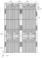
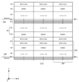
- FIG. 2B shows an example of a plurality of control blocks 220 according to the embodiment.
- the plurality of control blocks 220 of this example are arranged in reverse with each other adjacent to each other.
- the figure illustrates 12 control blocks 220 among a plurality of control blocks 220 provided in the main circuit unit 210.
- the region where each configuration of the control block 220 (for example, the exposure control unit 10, the pixel drive unit 20, the junction unit 30, the signal conversion unit 40, and the signal output unit 50) is formed is a boundary line between the blocks. It is shown that the mirrors are inverted around the center. That is, even the circuits of each configuration of the control block 220 do not have to be inverted. Further, the reading order of each pixel of the control block 220 is not limited to the one that is read in reverse.
- each configuration of the control block 220 is inverted and arranged in the row direction, so that the same configuration is arranged adjacent to each other at the boundary of the blocks. Will be.
- each configuration of the control block 220 is inverted and arranged in the column direction, so that the same configuration is arranged adjacent to each other at the boundary of the blocks. Will be done. Thereby, the layout efficiency of the control block 220 can be improved.
- the control block 220 is inverted with the adjacent control block 220.
- all control blocks 220 are inverted in the row and column directions, but may be inverted in either the row or column direction.
- the comparator 42 of the control block 220 is inverted with the comparator 42 of the control block 220 adjacent in the row direction.
- the comparator 42 of the control block 220 is also inverted with the comparator 42 of the control block 220 adjacent in the column direction.
- the storage unit 44 of the control block 220 is inverted with the storage unit 44 of the control block 220 adjacent to each other in the row direction and the column direction.
- the control block 220a and the control block 220b are provided adjacent to each other in the row direction.
- the control block 220a is inverted with the control block 220b.
- the level shift unit 14 of the control block 220a is provided in the same well region as the level shift unit 14 of the control block 220b.
- the local control unit 12, the storage unit 44, and the signal output unit 50 are provided in the same well region in the control block 220a and the control block 220b.
- the control block 220b and the control block 220c are provided adjacent to each other in the row direction.
- the control block 220b is inverted with the control block 220c.
- the pixel drive unit 20 of the control block 220b is provided in the same well region as the pixel drive unit 20 of the control block 220c.
- the well area of the pixel drive unit 20 may be shared with the well area of the level shift unit 14.
- the control block 220a and the control block 220d are provided adjacent to each other in the column direction.
- the control block 220a is inverted with the control block 220d.
- the pixel drive unit 20 of the control block 220a is provided in the same well region as the pixel drive unit 20 of the control block 220d.
- the signal conversion unit 40 of the control block 220a is provided in the same well region as the signal conversion unit 40 of the control block 220d.
- the control block 220d and the control block 220e are provided adjacent to each other in the column direction.
- the control block 220d is inverted with the control block 220e.
- the pixel drive unit 20 and the level shift unit 14 of the control block 220d are provided in the same well region as the pixel drive unit 20 and the level shift unit 14 of the control block 220e.
- the image sensor 400 of this example can improve the layout efficiency even when signal processing is performed in parallel for each control block 220.
- the image sensor 400 can share a well region between adjacent control blocks 220 by inverting a plurality of control blocks 220 on the XY plane. As a result, the number of times of switching the well area is reduced, and the area efficiency is improved.
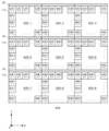
- FIG. 3 shows an example of a method of arranging the control block 720 according to the comparative example.
- the control block 720 of this example is not inverted with the adjacent control block 720.
- the control block 720 of this example is arranged by translating in the XY plane.
- the control block 720a and the control block 720b are provided adjacent to each other in the row direction.
- the control block 720a is not inverted with the control block 720b. Therefore, the signal conversion unit 40, the signal output unit 50, and the local control unit 12 of the control block 720a need to be provided in a well region different from the pixel drive unit 20 of the control block 720b. Therefore, a well separation region is provided between the control block 720a and the control block 720b.
- the control block 720a and the control block 720c are provided adjacent to each other in the Y-axis direction.
- the control block 720a is not inverted with the control block 720c. Therefore, the level shift unit 14 of the control block 720a needs to be provided in a well region different from the signal conversion unit 40 of the control block 720c.
- control block 720 of this example since the control block 720 of this example is not inverted, it is necessary to provide a well separation region at an adjacent portion on the XY plane.
- the layout size becomes larger than that in the case of inverting the arrangement as shown in FIG. 2B.
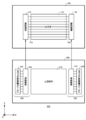
- FIG. 4 shows an example of the configuration of the image sensor 400.
- an example of the wiring method of the image pickup device 400 that functions as a block parallel ADC is shown.
- the pixel chip 100 includes connection areas 132 provided at both ends of the pixel unit 110.
- the signal processing chip 200 includes a connection region 232 and a global drive unit 234 provided in the peripheral circuit unit 230.
- the global drive unit 234 outputs a control signal for driving the pixel 112 to the connection area 232.
- the global drive unit 234 outputs the reset control signal ⁇ RST and the selection control signal ⁇ SEL as control signals.
- connection area 232 outputs a control signal from the global drive unit 234 to the connection area 132.
- connection area 232 is electrically connected to the connection area 132 by a conductive via or the like.
- connection area 132 outputs a control signal to the pixel unit 110 to control the drive of the pixel unit 110.
- the connection region 132 of this example outputs a control signal to the pixel unit 110 by the global control line 143 extending in the row direction. That is, the image sensor 400 of this example globally controls the pixel unit 110 by the reset control signal ⁇ RST and the selection control signal ⁇ SEL.
- the image sensor 400 of this example outputs a control signal from the signal processing chip 200 to the pixel chip 100, and then returns the pixel signal from the pixel unit 110 to the main circuit unit 210.
- the global drive unit 234 may be arranged on the pixel chip 100.
- FIG. 5 shows an example of the configuration of the image sensor 800 according to the comparative example.
- the pixel chip 600 includes a connection region 632 provided around the pixel unit 610.
- the signal processing chip 700 includes a connection region 732 and a global drive unit 734 provided around the main circuit unit 710.
- connection area 632a to the connection area 632d are connected to the connection area 732a to the connection area 732d, respectively.
- the connection area 632a and the connection area 632d input a control signal to the pixel unit 610.
- the pixel unit 610 outputs a pixel signal to the connection area 632b and the connection area 632c.
- the connection area 632b and the connection area 632c output the input pixel signal to the connection area 732b and the connection area 732c of the signal processing chip 200, respectively.
- the connection area 632b and the connection area 632c are provided around the pixel unit 610 and are connected to the pixel unit 610 by wiring extending in the row direction.
- FIG. 6A is a diagram for explaining an example of a wiring method for the image sensor 400.
- the global drive unit 234 of this example is provided in the peripheral circuit unit 230 arranged so as to sandwich both ends of the main circuit unit 210.
- the local control line 141 is connected to the pixel block 120a.
- the local control line 141 of this example is connected to the gate terminals of the first transfer unit 123 and the second transfer unit 124 provided in the pixel block 120a.
- the local control line 141 supplies the first transfer control signal ⁇ TX1 and the second transfer control signal ⁇ TX2 output from the control block 220a to the pixel block 120a.
- the local control line 141 is an example of a first control line connected to the first pixel of the pixel block 120.
- the local control line 141 may be provided corresponding to the pixel group 115 of the pixel block 120a. For example, in the pixel group 115, a common local control line 141 is connected to n pixels 112 arranged in the row direction.
- the local control line 142 is connected to the pixel block 120b.
- the local control line 142 of this example is connected to the gate terminals of the first transfer unit 123 and the second transfer unit 124 provided in the pixel block 120b.
- the local control line 142 supplies the first transfer control signal ⁇ TX1 and the second transfer control signal ⁇ TX2 output from the control block 220b to the pixel block 120b.
- the local control line 142 is an example of a second control line connected to the second pixel of the pixel block 120.
- the local control line 142 may be provided corresponding to the pixel group 115 of the pixel block 120b. For example, in the pixel group 115, a common local control line 142 is connected to n pixels 112 arranged in the row direction.
- the global drive unit 234 outputs a reset control signal ⁇ RST, a selection control signal ⁇ SEL, and a transfer selection control signal ⁇ TXSEL.
- the global drive unit 234 is connected to a global control line 143 that outputs a signal to each pixel block 120.
- the global drive unit 234 supplies the reset control signal ⁇ RST and the selection control signal ⁇ SEL to the plurality of pixel blocks 120 via the global control line 143.
- the global drive unit 234 supplies the transfer selection control signal ⁇ TXSEL to the plurality of control blocks 220 via the global control line 143.
- the transfer selection control signal ⁇ TXSEL is supplied from the global drive unit 234 to the control block 220 in order to control the exposure time for each pixel group 115.
- the control block 220 to which the transfer selection control signal ⁇ TXSEL is supplied outputs the transfer selection control signal ⁇ TXSEL to the corresponding pixel block 120.
- the pixel block 120 determines whether or not the transfer selection control signal ⁇ TXSEL is input to the pixel 112 as the first transfer control signal ⁇ TX1 or the second transfer control signal ⁇ TX2. As a result, the input of the first transfer control signal ⁇ TX1 or the second transfer control signal ⁇ TX2 to the pixel 112 is skipped.
- the control block 220 when the first transfer control signal ⁇ TX1 determines the end time of exposure, the control block 220 extends the exposure time by skipping the first transfer control signal ⁇ TX1. Further, when the first transfer control signal ⁇ TX1 determines the exposure start time, the control block 220 can shorten the exposure time by skipping the first transfer control signal ⁇ TX1. In this way, the exposure time of the pixel group 115 can be adjusted by the transfer selection control signal ⁇ TXSEL. The same applies when the second transfer control signal ⁇ TX2 determines the start time or end time of the exposure.
- the global control line 143 is commonly provided in the plurality of pixel blocks 120.
- the global control line 143 of this example is wired so as to cross the pixel chip 100 in the row direction.
- the global control line 143 may be wired so as to cross the pixel chip 100 in the column direction.
- the global control line 143 is an example of a third control line provided in common with the pixels connected to the local control line 141 and the pixels connected to the local control line 142.
- the global control line 143 is connected to the gate terminals of the reset unit 126 and the selection unit 129 of the pixel block 120, and supplies the reset control signal ⁇ RST and the selection control signal ⁇ SEL. Further, the global control line 143 is connected to each of the plurality of control blocks 220 and supplies the transfer selection control signal ⁇ TXSEL to the exposure control unit 10.
- the global drive unit 234 of this example outputs the transfer selection control signal ⁇ TXSEL from the signal processing chip 200 to the pixel chip 100
- the transfer selection control signal ⁇ TXSEL is sent to the control block 220 without being supplied to the pixel chip 100. You may output it.
- the global control line 143 is provided on the signal processing chip 200.
- the plurality of bumps 152 are provided on the joint surface where the pixel chip 100 and the signal processing chip 200 are joined to each other.
- the bump 152 of the pixel chip 100 is aligned with the bump 152 of the signal processing chip 200.
- the plurality of bumps 152 facing each other are joined by pressure processing or the like of the pixel chip 100 and the signal processing chip 200, and are electrically connected.
- the image sensor 400 of this example controls the exposure time for each pixel group 115 by changing at least one timing of the first transfer unit 123 and the second transfer unit 124 by a local control line.
- the image sensor 400 can realize the control of the exposure time with a smaller number of control lines.
- FIG. 6B is a diagram for explaining an example of the wiring method of the image pickup device 400.
- the wiring for inputting a pixel signal from the pixel 112 to the control block 220 is shown.
- the ground wiring GND is set to a predetermined reference potential GND.
- the ground wiring GND of this example is wired so as to cross the pixel chip 100 in the row direction.
- the ground wiring GND is connected to the joint portion 30 of the control block 220 via the bump 152.
- the joint portion 30 is connected to the output wiring of the voltage VPOUT and the power supply wiring of the voltage VDD.
- the joint portion 30 is connected to the ground wiring GND set to the reference potential VGND.
- the junction 30 outputs a pixel signal to a corresponding comparator 42.
- n comparators 42 are provided in the row direction.
- FIG. 7A shows an example of the joint surface 150 of the pixel chip 100 and the signal processing chip 200.
- four control blocks 220a to 220d indicate areas adjacent to each other.
- the bump 152a supplies the first transfer control signal ⁇ TX1, the second transfer control signal ⁇ TX2, and the transfer selection control signal ⁇ TXSEL.
- the bump 152a is provided at a position corresponding to the pixel drive unit 20.
- Bumps 152a are provided at the four corners of the square corresponding to each pixel 112.
- a dummy bump 154 may be provided at the center of the square provided with the four bumps 152a.
- the bumps 152a of this example are provided side by side in m (for example, 32) in the row direction.
- the bumps for supplying the transfer selection control signal ⁇ TXSEL may be shared by the control block 220a and the control block 220b.
- the bump 152b outputs a pixel signal from the pixel 112.
- the bump 152b is provided at a position corresponding to the joint portion 30.
- the bump 152b is provided in a region adjacent to the bump 152a and the dummy bump 154.
- the bump 152b of this example is provided at the center of the square corresponding to each pixel 112.
- the bumps 152b are provided in an array of n (for example, 16) in the row direction for one control block 220.
- the bump 152c is a bump for connecting the control block 220 to the ground voltage GND.
- the bump 152c is provided at a position corresponding to the joint portion 30.
- the bumps 152c of this example are provided at the two corners of the square corresponding to each pixel 112. For example, 14 bumps 152c are provided side by side in the row direction.
- the dummy bump 154 is arranged in an area where the bump 152 is not provided.
- the dummy bump 154 may be electrically isolated from the circuit.
- the dummy bump 154 of this example is regularly provided for each pixel 112, but is not limited to this.
- the dummy bump 154 may be provided to promote heat dissipation.
- the dummy bumps 154 of this example are provided at both the four corners of the square and the center of the square corresponding to each pixel 112.
- FIG. 7B shows an example of an enlarged view of the joint surface 150.
- the bump 152b is connected to the control block 220 by wiring 156.
- Wiring 156 connects the bump 152b and the signal conversion unit 40.
- N wirings 156 are provided corresponding to n bumps 152b arranged in the row direction.
- the n bumps 152b arranged in the row direction are connected to the comparator 42 arranged n in the row direction.
- the signal conversion unit 40 has a shorter width in the row direction because the pixel drive unit 20 is arranged. Therefore, the linear distance of the connection destination of the signal conversion unit 40 corresponding to the bump 152b is different in each wiring 156.
- the wiring 156 of this example is adjusted so that the lengths of the wiring 156 are equal to each other even if the linear distances at both ends of the wiring 156 are different. As a result, the delay between the pixels of the pixel signal output from the pixel 112 can be eliminated, and the pixel signal can be uniformly output for each column. In this example, the delay between the pixels is eliminated by changing the length of the wiring 156, but the delay between the pixels may be eliminated by changing the width of the wiring 156.
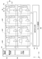
- FIG. 8A shows an example of the configuration of the pixel unit 110 according to the embodiment.
- the pixel block 120 of this example has a plurality of pixels 112 and a junction 30.
- the pixel block 120 has m ⁇ n pixels 112.
- nine pixel blocks 120-1 to 120-9 will be illustrated and described.
- a case where the pixel block 120 is provided in a one-to-one correspondence with the pixel group 115 will be described.
- the pixel block 120 is inverted.
- the pixel block 120-1 is inverted with the pixel block 120-4. Therefore, the joint portion 30 of the pixel block 120-1 is arranged adjacent to the joint portion of the pixel block 120-4. Thereby, the layout efficiency can be improved.
- FIG. 8B shows an example of the configuration of the main circuit unit 210 according to the embodiment.
- the control block 220 of this example includes a joint portion 30, a signal conversion unit 40, and a signal output unit 50.
- the signal conversion unit 40 includes a comparator 42 and a storage unit 44.
- nine control blocks 220 will be illustrated and described.
- the input analog signal is indicated by a straight arrow, and the output digital signal is indicated by a broken arrow.
- the comparator 42 converts the image signal input from the pixel chip 100 into a digital signal.
- the comparator 42 is provided adjacent to the junction 30.
- the storage unit 44 stores the digital signal from the comparator 42.
- the storage unit 44 is provided adjacent to the comparator 42.
- the signal output unit 50 outputs the digital signal output by the comparator 42 in a predetermined output direction (for example, the row direction).
- a digital signal stored in the storage unit 44 is input to the signal output unit 50 of this example.
- the signal output unit 50 is connected to an output wiring wired so as to cross the main circuit unit 210 in the row direction.
- the signal output units 50 of the control blocks 220 adjacent to each other in the column direction can be arranged together. As a result, the digital signal lines can be arranged together, and the layout efficiency is improved.
- the joining portion 30 joins the pixel chip 100 and the signal processing chip 200.
- the joints 30 are inverted in the row direction.
- the junction 30 and the comparator 42 of the control blocks 220 adjacent to each other in the column direction can be arranged together.
- the joining portion 30 of this example is provided by stretching in a predetermined stretching direction (for example, the row direction), and connects the pixel chip 100 and the signal processing chip 200.
- the joint portion 30 and the storage portion 44 of this example are invertedly arranged in the control block 220 adjacent to the control block 220 in a direction different from the stretching direction (for example, the row direction).
- the junction 30 is also reversed in the control block 220 adjacent to the comparator 42 and the storage 44 of this example in a direction different from the output direction (for example, the column direction).
- the junction 30 and the comparator 42 have an analog signal line as an ADC input unit.
- the storage unit 44 and the signal output unit 50 have a digital signal line that handles the signal after AD conversion. Therefore, the main circuit unit 210 can secure a space between the analog signal line and the digital signal line between the plurality of adjacent control blocks 220 and suppress the mixing of digital noise.
- FIG. 8C shows an example of the main circuit unit 210 corresponding to the pixel unit 110 of FIG. 8A.
- the image pickup device 400 includes a plurality of control wirings 240.
- the case where the plurality of control wirings 240 are extended in the row direction will be described, but the case where the plurality of control wirings 240 are extended in the column direction is also applied by changing the direction of the inverted arrangement of the control blocks 220. can do.
- the control wiring 240 is provided so as to extend in a predetermined wiring direction (for example, the row direction).
- the control wiring 240 of the plurality of control blocks 220 arranged side by side in the wiring direction is shared with the control wiring 240 of the control block 220 adjacent in a direction different from the wiring direction (for example, the column direction). Is provided.
- the number of control wiring 240 can be reduced.
- FIG. 9A shows an example of the configuration of the pixel unit 610 according to the comparative example.
- the pixel blocks 620 are not arranged in reverse. That is, each of the pixel blocks 620 is arranged by translating in the XY plane.
- FIG. 9B shows an example of the configuration of the main circuit unit 710 according to the comparative example.
- the control block 720 is not inverted. Therefore, a junction 30 to which an analog signal is input and a signal output unit 50 to output a digital signal are provided adjacent to each other in the column direction. As a result, in the main circuit unit 710, the analog signal line and the digital signal line may interfere with each other.
- FIG. 9C shows an example of the configuration of the main circuit unit 710 according to the comparative example.
- the control block 720 is not inverted. Therefore, it is necessary to provide the control wiring 740 in each of the control blocks 720. Therefore, the number of control wiring 740 cannot be reduced.
- FIG. 10A shows an example of a timing chart showing the image pickup operation of the image pickup device 400.
- an example of the control method of the reset control signal ⁇ RST, the first transfer control signal ⁇ TX1, and the selection control signal ⁇ SEL is shown.
- the first transfer control signal ⁇ TX1 and the control signal Reset control the timing at which exposure is started.
- the exposure start timing is the falling timing (time T1) of the first transfer control signal ⁇ TX1 and the control signal Reset.
- Turning on the control signal Reset corresponds to turning on both the reset control signal ⁇ RST and the second transfer control signal ⁇ TX2.
- the second transfer control signal ⁇ TX2 is a locally controlled signal.
- the first transfer control signal ⁇ TX1 transfers the electric charge accumulated in the photoelectric conversion unit 104 to the storage unit 125 by turning on the first transfer unit 123.
- the first transfer control signal ⁇ TX1 controls the timing at which the exposure ends.
- the end timing of the exposure is the falling timing (time T3) of the first transfer control signal ⁇ TX1. Since the first transfer control signal ⁇ TX1 of this example is a globally controlled signal, the timing of ending the exposure in each pixel group 115 is the same. Further, the first transfer control signal ⁇ TX1 discharges the electric charge left in the photoelectric conversion unit 104 by turning on the first transfer unit 123 at the same time as the control signal Reset.
- the selection control signal ⁇ SEL is a signal for selecting an arbitrary pixel 112.
- the selection control signal ⁇ SEL controls the on / off of the selection unit 129.
- the selection control signal ⁇ SEL is set high.
- the pixel 112 in which the selection control signal ⁇ SEL is set to high outputs a pixel signal to the signal line 122 in response to the on of the first transfer control signal ⁇ TX1.
- the pixel signal is not output to the pixel 112 in which the selection control signal ⁇ SEL is not set to high.
- the image sensor 400 of this example can change the exposure start timing for each pixel group 115 and control the exposure time for each pixel group 115. Further, the image sensor 400 may control the end timing of the exposure for each pixel group 115 by locally controlling the first transfer control signal ⁇ TX1. Then, the image sensor 400 may control both the start timing and the end timing of the exposure for each pixel group 115 by locally controlling both the first transfer control signal ⁇ TX1 and the second transfer control signal ⁇ TX2.
- FIG. 10B shows an example of the exposure timing for each pixel group 115.
- the exposure time of the four pixel groups 115 is controlled for each pixel group 115.
- the image sensor 400 changes the exposure amount by shifting the pixel reset time for each pixel group 115. Therefore, in each pixel group 115, the end time of exposure (that is, the read time) is the same, but the start time of exposure (that is, the pixel reset time) is changed. As a result, the image sensor 400 can set each pixel group 115 to a different exposure time.
- the vertical synchronization signal (XVS) and the horizontal synchronization signal (XHS) control the reading of image data by the image sensor 400.
- the vertical synchronization signal is switched at a timing corresponding to the number of pixels in the column direction of the control block 220.
- the horizontal synchronization signal is switched at a timing corresponding to the number of pixels in the row direction of the control block 220.
- the read data may be output as image data in subsequent frames.
- FIG. 11A shows an example of the configuration of the signal processing chip 200.
- the control block 220 includes a logic circuit 60 and an analog circuit 65.
- the logic circuit 60 has a latch 61 and a selector 62.
- the analog circuit 65 has a level shifter 66 and a buffer 67.
- the global drive unit 234 of this example has a selection signal generation unit 236 and a reset pulse generation unit 238.
- the selection signal generation unit 236 inputs a selection signal for selecting the pixel 112 to the latch 61.
- the reset pulse generation unit 238 inputs the transfer selection control signal ⁇ TXSEL to the selector 62.
- the selection signal generation unit 236 and the reset pulse generation unit 238 output digital signals.
- the logic circuit 60 is composed of transistors for processing digital signals.
- the logic circuit 60 operates in response to the digital signals input from the selection signal generation unit 236 and the reset pulse generation unit 238.
- the analog circuit 65 is composed of transistors for processing analog signals.
- the level shifter 66 converts the digital signal input from the logic circuit 60 into an analog signal.
- the buffer 67 outputs an analog signal to the pixel portion 110 through the junction portion 30.
- the analog circuit 65 of this example is arranged together in four control blocks 220 adjacent to each other in the row direction and the column direction. Thereby, the layout efficiency can be improved.
- the joints 30 are arranged together in four control blocks 220 adjacent to each other in the row direction and the column direction. That is, since the prohibited areas around the joint portion 30 can be arranged together, the layout can be facilitated and the circuit area can be reduced.
- the level shifter 66 is arranged for each control block 220, the latch 61 and the selector 62 can be configured by a digital transistor. As a result, the circuit area can be reduced as compared with the case where the logic circuit 60 is composed of analog transistors. Further, since the signal processing chip 200 can arrange the level shifter 66 in the immediate vicinity of the pixel unit 110, the output load can be reduced and the circuit scale of the level shifter 66 can be reduced.
- FIG. 11B shows an example of a cross-sectional view of the signal processing chip 200.
- the cross-sectional view of this example is an example of an XZ cross-sectional view passing through the logic circuit 60 and the analog circuit 65.
- the semiconductor substrate 260 has a first well region 261 and a second well region 262.
- the semiconductor substrate 260 is P type
- the first well region 261 is N type
- the second well region 262 is P type, but the present invention is not limited thereto.
- Circuits such as transistors constituting the signal processing chip 200 are formed in the first well region 261 and the second well region 262.
- the well separation region 263 is provided to separate the adjacent first well region 261.
- the well separation region 263 separates the first well region 261 at intervals of a predetermined size or more according to the manufacturing process rules.
- the signal processing chip 200 of this example can reduce the number of well separation regions 263 required to separate the first well region 261.
- the signal processing chip 200 can share the well separation region 263 by providing the level shifter 66 of the control block 220 adjacent in the row direction or the column direction in the common well region. As a result, the circuit area of the signal processing chip 200 can be reduced.
- FIG. 12A shows an example of the configuration of the signal processing chip 700 according to the comparative example.
- the global drive unit 734 includes a selection signal generation unit 736 and a reset pulse generation unit 738.
- the level shifter 66 is arranged around the control block 720.
- the level shifter 66 inputs an analog signal to the control block 720. Therefore, in the control block 720, the logic circuit 60 needs to be composed of analog transistors. Therefore, the circuit area of the control block 720 becomes large.
- FIG. 12B shows another example of the signal processing chip 700 according to the comparative example.
- the level shifter 66 is provided inside the control block 720, but the control block 720 is not inverted. Therefore, the logic circuit 60 or the analog circuit 65 cannot be arranged together in the adjacent control block 720.
- FIG. 12C shows an example of a cross-sectional view of the signal processing chip 700 according to the comparative example.
- a comparative example in which substantially the same number of logic circuits 60 and analog circuits 65 are provided as in FIG. 11B is shown.
- the number of well separation regions 263 required increases. For example, in the case of FIG. 11B, when it is necessary to provide two well separation regions 263, in FIG. 12C, five well separation regions 263 are required.
- the circuit area increases as the number of times the well separation region 263 is provided increases.
- FIG. 13 is a block diagram showing a configuration example of the imaging device 500 according to the embodiment.
- the image sensor 500 includes an image sensor 400, a system control unit 501, a drive unit 502, a photometric unit 503, a work memory 504, a recording unit 505, a display unit 506, a drive unit 514, and a photographing lens 520. To be equipped.
- the photographing lens 520 guides the subject luminous flux incident along the optical axis OA to the image sensor 400.
- the photographing lens 520 is composed of a plurality of optical lens groups, and forms a subject light flux from the scene in the vicinity of the focal plane thereof.
- the photographing lens 520 may be an interchangeable lens that can be attached to and detached from the image pickup apparatus 500.
- one virtual lens arranged near the pupil represents the photographing lens 520.
- the drive unit 514 drives the photographing lens 520.
- the drive unit 514 moves the optical lens group of the photographing lens 520 to change the focusing position.
- the drive unit 514 may drive the iris diaphragm in the photographing lens 520 to control the amount of light of the subject luminous flux incident on the image sensor 400.
- the drive unit 502 has a control circuit that executes charge accumulation control such as timing control and area control of the image pickup device 400 according to an instruction from the system control unit 501. Further, the operation unit 508 receives an instruction from the imager by using a release button or the like.
- the image sensor 400 delivers the pixel signal to the image processing unit 511 of the system control unit 501.
- the image processing unit 511 uses the work memory 504 as a workspace to generate image data subjected to various image processing. For example, when generating image data in JPEG file format, a compression process is executed after generating a color video signal from the signal obtained in the Bayer array.
- the generated image data is recorded in the recording unit 505, converted into a display signal, and displayed on the display unit 506 for a preset time.
- the photometric unit 503 detects the brightness distribution of the scene prior to a series of shooting sequences that generate image data.
- the light measuring unit 503 includes, for example, an AE sensor having about 1 million pixels.
- the calculation unit 512 of the system control unit 501 receives the output of the photometric unit 503 and calculates the brightness for each area of the scene.
- the calculation unit 512 determines the shutter speed, aperture value, and ISO sensitivity according to the calculated luminance distribution.
- the light measuring unit 503 may also be used by the image sensor 400.
- the calculation unit 512 also executes various calculations for operating the image pickup apparatus 500.
- the drive unit 502 may be partially or wholly mounted on the image sensor 400.
- a part of the system control unit 501 may be mounted on the image sensor 400.
- the comparator corresponding to the first pixel block among the plurality of pixels is an image sensor that is inverted with respect to the comparator corresponding to the second pixel block adjacent to the first pixel block.
- the image pickup device according to item 1 wherein the storage unit corresponding to the first pixel block is inverted with respect to the storage unit corresponding to the second pixel block.
- a pixel chip having the pixel portion and A signal processing chip that is laminated with the pixel chip and processes a pixel signal from the pixel portion is provided.
- the image pickup device according to item 1 or 2 wherein the signal processing chip has a plurality of control blocks provided corresponding to the pixel blocks of the plurality of pixels.
- the plurality of control blocks have a joint portion for stretching in a predetermined stretching direction and connecting to the pixel chip.
- the image pickup device according to any one of items 3 to 6, wherein the storage unit and the joint portion are inverted and arranged in the plurality of control blocks adjacent to each other in a direction different from the stretching direction.
- the plurality of control blocks have a signal output unit for outputting the digital signal output by the comparator in a predetermined output direction.
- the image pickup device according to any one of items 3 to 7, wherein the comparator and the signal output unit are inverted and arranged in the plurality of control blocks adjacent to each other in a direction different from the output direction.
- [Item 9] Equipped with control wiring provided by extending in a predetermined wiring direction, The image pickup device according to any one of items 3 to 8, wherein the control wiring is shared by the plurality of control blocks adjacent to each other in a direction different from the wiring direction.
- An image pickup apparatus comprising the image pickup device according to any one of items 1 to 9.
- a pixel part having a plurality of pixels and A signal conversion unit that digitally converts the analog signal output by the pixel unit, and An exposure control unit that controls the exposure of the plurality of pixels, A pixel drive unit for driving the plurality of pixels is provided.
- the pixel drive unit is stretched in a predetermined first direction, and the exposure control unit is stretched in a second direction different from the first direction, so that the pixel drive unit and the exposure control unit are L-shaped.
- a pixel chip having the pixel portion and A signal processing chip that is laminated with the pixel chip and has the signal conversion unit is provided.
- the L-shaped pixel drive unit and the exposure control unit constitute an outer circumference of the control block.
- the exposure control unit A local control unit extending in the second direction and The image pickup device according to item 12 or 13, further extending in the second direction and having a level shift unit provided on the outer peripheral side of the control block with respect to the local control unit.
- the image pickup device according to item 14 wherein the level shift portion of the adjacent control block is provided in the same well region.
- the signal processing chip The first control block and A second control block provided adjacent to the first control block is provided.
- the signal conversion unit has a comparator that converts the analog signal into a digital signal.
- the image pickup device according to any one of items 12 to 16, wherein the comparator of the first control block is inverted with respect to the comparator of the second control block.
- Item 17 The image pickup device according to item 17, wherein the comparator of the first control block is inverted with the comparator of a third control block adjacent to the first control block in a second direction orthogonal to the first direction.
- the signal conversion unit includes a storage unit that stores a digital signal output by the comparator.
- the image pickup device according to item 17 or 18, wherein the storage unit of the first control block is inverted with respect to the storage unit of the second control block.
- An image pickup apparatus comprising the image pickup device according to any one of items 11 to 19.
- Connection area 700. ⁇ ⁇ Signal processing chip, 710 ⁇ ⁇ ⁇ Main circuit unit, 720 ⁇ ⁇ ⁇ Control block, 732 ⁇ ⁇ ⁇ Connection area, 734 ⁇ ⁇ ⁇ Global drive unit, 736 ⁇ ⁇ ⁇ Selection signal generation unit, 738 ⁇ ⁇ ⁇ Reset Pulse generator, 740 ... control wiring, 800 ... image pickup element
Landscapes
- Engineering & Computer Science (AREA)
- Multimedia (AREA)
- Signal Processing (AREA)
- Transforming Light Signals Into Electric Signals (AREA)
- Solid State Image Pick-Up Elements (AREA)
- Vehicle Body Suspensions (AREA)
- Apparatus For Radiation Diagnosis (AREA)
Abstract
Description
特許文献1 国際公開第2017/018188号
[項目1]
複数の画素を有する画素部と、
前記画素部が出力したアナログ信号をデジタル信号に変換するコンパレータと、
前記デジタル信号を記憶する記憶部と
を備え、
前記複数の画素のうち第1画素ブロックに対応する前記コンパレータは、前記第1画素ブロックと隣接する第2画素ブロックに対応する前記コンパレータに対して反転配置される
撮像素子。
[項目2]
前記第1画素ブロックに対応する前記記憶部は、前記第2画素ブロックに対応する前記記憶部に対して反転配置される
項目1に記載の撮像素子。
[項目3]
前記画素部を有する画素チップと、
前記画素チップと積層され、前記画素部からの画素信号を処理する信号処理チップと
を備え、
前記信号処理チップは、前記複数の画素の画素ブロックにそれぞれ対応して設けられた複数の制御ブロックを有する
項目1または2に記載の撮像素子。
[項目4]
前記複数の制御ブロックのうち第1制御ブロックの前記コンパレータは、予め定められた第1方向において、前記第1制御ブロックと隣接する第2制御ブロックの前記コンパレータと反転配置されている
項目3に記載の撮像素子。
[項目5]
前記第1制御ブロックの前記コンパレータは、前記第1方向と直交する第2方向において前記第1画素ブロックと隣接する第3制御ブロックの前記コンパレータと反転配置されている
項目4に記載の撮像素子。
[項目6]
前記複数の制御ブロックは、電圧レベルを変換するレベルシフト部を有し、
前記複数の制御ブロックのうち隣接する制御ブロックの前記レベルシフト部は、同一のウェル領域内に設けられる
項目3から5のいずれか一項に記載の撮像素子。
[項目7]
前記複数の制御ブロックは、予め定められた延伸方向に延伸し、前記画素チップと接続するための接合部を有し、
前記記憶部および前記接合部は、前記延伸方向と異なる方向に隣接した前記複数の制御ブロックにおいて、反転配置されている
項目3から6のいずれか一項に記載の撮像素子。
[項目8]
前記複数の制御ブロックは、前記コンパレータが出力した前記デジタル信号を、予め定められた出力方向に出力するための信号出力部を有し、
前記コンパレータおよび前記信号出力部は、前記出力方向と異なる方向に隣接した前記複数の制御ブロックにおいて、反転配置されている
項目3から7のいずれか一項に記載の撮像素子。
[項目9]
予め定められた配線方向に延伸して設けられた制御配線を備え、
前記制御配線は、前記配線方向と異なる方向に隣接した前記複数の制御ブロックにおいて、共有して設けられる
項目3から8のいずれか一項に記載の撮像素子。
[項目10]
項目1から9のいずれか一項に記載の撮像素子を備える撮像装置。
[項目11]
複数の画素を有する画素部と、
前記画素部が出力したアナログ信号をデジタル変換する信号変換部と、
前記複数の画素の露光を制御する露光制御部と、
前記複数の画素を駆動する画素駆動部と
を備え、
前記画素駆動部が予め定められた第1方向に延伸し、前記露光制御部が前記第1方向と異なる第2方向に延伸することにより、前記画素駆動部および前記露光制御部がL字型に配置される
撮像素子。
[項目12]
前記画素部を有する画素チップと、
前記画素チップと積層され、前記信号変換部を有する信号処理チップと
を備え、
前記信号処理チップは、前記複数の画素の画素ブロックにそれぞれ対応して設けられた制御ブロックを有する
項目11に記載の撮像素子。
[項目13]
前記L字型の前記画素駆動部および前記露光制御部は、前記制御ブロックの外周を構成する
項目12に記載の撮像素子。
[項目14]
前記露光制御部は、
前記第2方向に延伸して設けられたローカル制御部と、
前記第2方向に延伸し、前記ローカル制御部よりも前記制御ブロックの外周側に設けられたレベルシフト部と
を有する
項目12または13に記載の撮像素子。
[項目15]
隣接する前記制御ブロックの前記レベルシフト部は、同一のウェル領域内に設けられる
項目14に記載の撮像素子。
[項目16]
前記信号変換部と前記露光制御部との間に設けられ、前記デジタル変換された信号を出力する信号出力部を備える
項目12から15のいずれか一項に記載の撮像素子。
[項目17]
前記信号処理チップは、
第1制御ブロックと、
前記第1制御ブロックと隣接して設けられた第2制御ブロックと
を備え、
前記信号変換部は、前記アナログ信号をデジタル信号に変換するコンパレータを有し、
前記第1制御ブロックの前記コンパレータは、前記第2制御ブロックの前記コンパレータに対して反転配置される
項目12から16のいずれか一項に記載の撮像素子。
[項目18]
前記第1制御ブロックの前記コンパレータは、前記第1方向と直交する第2方向において前記第1制御ブロックと隣接する第3制御ブロックの前記コンパレータと反転配置されている
項目17に記載の撮像素子。
[項目19]
前記信号変換部は、前記コンパレータが出力したデジタル信号を記憶する記憶部を備え、
前記第1制御ブロックの前記記憶部は、前記第2制御ブロックの前記記憶部に対して反転配置される
項目17または18に記載の撮像素子。
[項目20]
項目11から19のいずれか一項に記載の撮像素子を備える撮像装置。
Claims (13)
- 1または複数の画素を含む複数の画素ブロックを有する画素チップと、
複数の前記画素ブロックのうち少なくとも第1画素ブロックに含まれる画素からの信号をデジタル信号に変換する第1変換部と前記第1変換部で変換されたデジタル信号を記憶する第1記憶部とを含む第1制御ブロックと、列方向において前記第1制御ブロックの隣に配置され、複数の前記画素ブロックのうち少なくとも第2画素ブロックに含まれる画素からの信号をデジタル信号に変換する第2変換部と前記第2変換部で変換されたデジタル信号を記憶する第2記憶部とを含む第2制御ブロックとを有する信号処理チップと、
を備え、
前記第2制御ブロックにおける前記第2変換部および前記第2記憶部は、前記第1制御ブロックにおける前記第1変換部および前記第1記憶部の配置位置に対して上下反転させた位置に配置される、
撮像素子。 - 前記第1制御ブロックは、前記第1画素ブロックに含まれる画素の露光時間を制御するための第1露光制御部を有し、
前記第2制御ブロックは、前記第2画素ブロックに含まれる画素の露光時間を制御するための第2露光制御部を有し、
前記第2制御ブロックにおける前記第2変換部、前記第2記憶部および前記第2露光制御部は、前記第1制御ブロックにおける前記第1変換部、前記第1記憶部および前記第1露光制御部の配置位置に対して上下反転させた位置に配置される、
請求項1に記載の撮像素子。 - 前記第1制御ブロックは、前記第1画素ブロックに含まれる画素を駆動させるための第1画素駆動部を有し、
前記第2制御ブロックは、前記第2画素ブロックに含まれる画素を駆動させるための第2画素駆動部を有し、
前記第2制御ブロックにおける前記第2変換部、前記第2記憶部、前記第2露光制御部および前記第2画素駆動部は、前記第1制御ブロックにおける前記第1変換部、前記第1記憶部、前記第1露光制御部および前記第1画素駆動部の配置位置に対して上下反転させた位置に配置される、
請求項2に記載の撮像素子。 - 前記第1制御ブロックは、電圧レベルを変換する第1レベルシフト部を有し、
前記第2制御ブロックは、電圧レベルを変換する第2レベルシフト部を有し、
前記第2制御ブロックにおける前記第2変換部、前記第2記憶部、前記第2露光制御部、前記第2画素駆動部および前記第2レベルシフト部は、前記第1制御ブロックにおける前記第1変換部、前記第1記憶部、前記第1露光制御部、前記第1画素駆動部および前記第1レベルシフト部の配置位置に対して上下反転させた位置に配置される、
請求項3に記載の撮像素子。 - 前記信号処理チップは、行方向において前記第1制御ブロックの隣に配置され、複数の前記画素のうち少なくとも第3画素ブロックに含まれる画素からの信号をデジタル信号に変換する第3変換部と前記第3変換部で変換されたデジタル信号を記憶する第3記憶部とを含む第3制御ブロックを有し、
前記第3制御ブロックにおける前記第3変換部および前記第3記憶部は、前記第1制御ブロックにおける前記第1変換部および前記第1記憶部の配置位置に対して左右反転させた位置に配置される、
請求項1に記載の撮像素子。 - 前記第1制御ブロックは、前記第1画素ブロックに含まれる画素の露光時間を制御するための第1露光制御部を有し、
前記第2制御ブロックは、前記第2画素ブロックに含まれる画素の露光時間を制御するための第2露光制御部を有し、
前記第3制御ブロックは、前記第3画素ブロックに含まれる画素の露光時間を制御するための第3露光制御部を有し、
前記第2制御ブロックにおける前記第2変換部、前記第2記憶部および前記第2露光制御部は、前記第1制御ブロックにおける前記第1変換部、前記第1記憶部および前記第1露光制御部の配置位置に対して上下反転させた位置に配置され、
前記第3制御ブロックにおける前記第3変換部、前記第3記憶部および前記第3露光制御部は、前記第1制御ブロックにおける前記第1変換部、前記第1記憶部および前記第1露光制御部の配置位置に対して左右反転させた位置に配置される、
請求項5に記載の撮像素子。 - 前記第1制御ブロックは、前記第1画素ブロックに含まれる画素を駆動させるための第1画素駆動部を有し、
前記第2制御ブロックは、前記第2画素ブロックに含まれる画素を駆動させるための第2画素駆動部を有し、
前記第3制御ブロックは、前記第3画素ブロックに含まれる画素を駆動させるための第3画素駆動部を有し、
前記第2制御ブロックにおける前記第2変換部、前記第2記憶部、前記第2露光制御部および前記第2画素駆動部は、前記第1制御ブロックにおける前記第1変換部、前記第1記憶部、前記第1露光制御部および前記第1画素駆動部の配置位置に対して上下反転させた位置に配置され、
前記第3制御ブロックにおける前記第3変換部、前記第3記憶部、前記第3露光制御部および前記第3画素駆動部は、前記第1制御ブロックにおける前記第1変換部、前記第1記憶部、前記第1露光制御部および前記第1画素駆動部の配置位置に対して左右反転させた位置に配置される、
請求項6に記載の撮像素子。 - 前記第1制御ブロックは、電圧レベルを変換する第1レベルシフト部を有し、
前記第2制御ブロックは、電圧レベルを変換する第2レベルシフト部を有し、
前記第3制御ブロックは、電圧レベルを変換する第3レベルシフト部を有し、
前記第2制御ブロックにおける前記第2変換部、前記第2記憶部、前記第2露光制御部、前記第2画素駆動部および前記第2レベルシフト部は、前記第1制御ブロックにおける前記第1変換部、前記第1記憶部、前記第1露光制御部、前記第1画素駆動部および前記第1レベルシフト部の配置位置に対して上下反転させた位置に配置され、
前記第3制御ブロックにおける前記第3変換部、前記第3記憶部、前記第3露光制御部、前記第3画素駆動部および前記第3レベルシフト部は、前記第1制御ブロックにおける前記第1変換部、前記第1記憶部、前記第1露光制御部、前記第1画素駆動部および前記第1レベルシフト部の配置位置に対して左右反転させた位置に配置される、
請求項7に記載の撮像素子。 - 1または複数の画素を含む複数の画素ブロックを有する画素チップと、
複数の前記画素ブロックのうち少なくとも第1画素ブロックに含まれる画素からの信号をデジタル信号に変換する第1変換部と前記第1変換部で変換されたデジタル信号を記憶する第1記憶部と前記第1画素ブロックに含まれる画素の露光時間を制御するための第1露光制御部とを含む第1制御ブロックと、行方向において前記第1制御ブロックの隣に配置され、複数の前記画素ブロックのうち少なくとも第2画素ブロックに含まれる画素からの信号をデジタル信号に変換する第2変換部と前記第2変換部で変換されたデジタル信号を記憶する第2記憶部と前記第2画素ブロックに含まれる画素の露光時間を制御するための第2露光制御部とを含む第2制御ブロックとを有する信号処理チップと、
を備え、
前記第2制御ブロックにおける前記第2変換部および前記第2記憶部は、前記第1制御ブロックにおける前記第1変換部および前記第1記憶部の配置位置に対して左右反転させた位置に配置される、
撮像素子。 - 前記第1制御ブロックは、前記第1画素ブロックに含まれる画素を駆動させるための第1画素駆動部を有し、
前記第2制御ブロックは、前記第2画素ブロックに含まれる画素を駆動させるための第2画素駆動部を有し、
前記第2制御ブロックにおける前記第2変換部、前記第2記憶部、前記第2露光制御部および前記第2画素駆動部は、前記第1制御ブロックにおける前記第1変換部、前記第1記憶部、前記第1露光制御部および前記第1画素駆動部の配置位置に対して左右反転させた位置に配置される、
請求項9に記載の撮像素子。 - 前記第1制御ブロックは、電圧レベルを変換する第1レベルシフト部を有し、
前記第2制御ブロックは、電圧レベルを変換する第2レベルシフト部を有し、
前記第2制御ブロックにおける前記第2変換部、前記第2記憶部、前記第2露光制御部、前記第2画素駆動部および前記第2レベルシフト部は、前記第1制御ブロックにおける前記第1変換部、前記第1記憶部、前記第1露光制御部、前記第1画素駆動部および前記第1レベルシフト部の配置位置に対して左右反転させた位置に配置される、
請求項10に記載の撮像素子。 - 前記画素は、
光を電荷に変換する光電変換部と、
前記光電変換部の電荷を転送する転送部と、
前記転送部により転送された電荷を蓄積する蓄積部と、
前記蓄積部の電荷を排出するリセット部と、
を有する、
請求項1から請求項11のいずれか一項に記載の撮像素子。 - 請求項1から12のいずれか一項に記載の撮像素子を備える撮像装置。
Priority Applications (9)
| Application Number | Priority Date | Filing Date | Title |
|---|---|---|---|
| CN202180014844.XA CN115136585B (zh) | 2020-02-17 | 2021-02-17 | 摄像元件及摄像装置 |
| US17/800,433 US12225313B2 (en) | 2020-02-17 | 2021-02-17 | Image capturing device and image capturing apparatus |
| KR1020227028294A KR102959131B1 (ko) | 2020-02-17 | 2021-02-17 | 촬상 소자 및 촬상 장치 |
| CN202511190225.2A CN121056756A (zh) | 2020-02-17 | 2021-02-17 | 摄像元件及摄像装置 |
| JP2022501950A JP7491364B2 (ja) | 2020-02-17 | 2021-02-17 | 撮像素子及び撮像装置 |
| CN202511190179.6A CN121056755A (zh) | 2020-02-17 | 2021-02-17 | 摄像元件及摄像装置 |
| EP21756949.0A EP4109887A4 (en) | 2020-02-17 | 2021-02-17 | Imaging element and imaging device |
| JP2024079923A JP2024105586A (ja) | 2020-02-17 | 2024-05-16 | 撮像素子及び撮像装置 |
| US18/959,840 US20250088771A1 (en) | 2020-02-17 | 2024-11-26 | Image capturing device and image capturing apparatus |
Applications Claiming Priority (4)
| Application Number | Priority Date | Filing Date | Title |
|---|---|---|---|
| JP2020024781 | 2020-02-17 | ||
| JP2020-024780 | 2020-02-17 | ||
| JP2020024780 | 2020-02-17 | ||
| JP2020-024781 | 2020-02-17 |
Related Child Applications (2)
| Application Number | Title | Priority Date | Filing Date |
|---|---|---|---|
| US17/800,433 A-371-Of-International US12225313B2 (en) | 2020-02-17 | 2021-02-17 | Image capturing device and image capturing apparatus |
| US18/959,840 Continuation US20250088771A1 (en) | 2020-02-17 | 2024-11-26 | Image capturing device and image capturing apparatus |
Publications (1)
| Publication Number | Publication Date |
|---|---|
| WO2021166979A1 true WO2021166979A1 (ja) | 2021-08-26 |
Family
ID=77391259
Family Applications (1)
| Application Number | Title | Priority Date | Filing Date |
|---|---|---|---|
| PCT/JP2021/006011 Ceased WO2021166979A1 (ja) | 2020-02-17 | 2021-02-17 | 撮像素子及び撮像装置 |
Country Status (5)
| Country | Link |
|---|---|
| US (2) | US12225313B2 (ja) |
| EP (1) | EP4109887A4 (ja) |
| JP (2) | JP7491364B2 (ja) |
| CN (3) | CN121056755A (ja) |
| WO (1) | WO2021166979A1 (ja) |
Families Citing this family (2)
| Publication number | Priority date | Publication date | Assignee | Title |
|---|---|---|---|---|
| JP7844128B2 (ja) * | 2021-10-12 | 2026-04-13 | キヤノン株式会社 | 半導体装置 |
| US20240422453A1 (en) * | 2021-11-01 | 2024-12-19 | Sony Semiconductor Solutions Corporation | Physical quantity detecting device and imaging device |
Citations (5)
| Publication number | Priority date | Publication date | Assignee | Title |
|---|---|---|---|---|
| JP2013051674A (ja) * | 2011-08-02 | 2013-03-14 | Canon Inc | 周辺回路を配置しチップ面積増大を抑制した撮像素子及び撮像装置 |
| JP2015154413A (ja) * | 2014-02-18 | 2015-08-24 | ソニー株式会社 | 情報処理装置、情報処理方法、情報処理システム、および撮像装置 |
| WO2017018188A1 (ja) | 2015-07-24 | 2017-02-02 | ソニーセミコンダクタソリューションズ株式会社 | イメージセンサ、及び、電子機器 |
| JP2017192056A (ja) * | 2016-04-14 | 2017-10-19 | ソニー株式会社 | 固体撮像素子、撮像装置、および電子機器 |
| WO2017209221A1 (ja) * | 2016-05-31 | 2017-12-07 | ソニーセミコンダクタソリューションズ株式会社 | 撮像装置および撮像方法、カメラモジュール、並びに電子機器 |
Family Cites Families (12)
| Publication number | Priority date | Publication date | Assignee | Title |
|---|---|---|---|---|
| JPS60182164A (ja) * | 1984-02-28 | 1985-09-17 | Nec Corp | 固体撮像装置 |
| US7128270B2 (en) * | 1999-09-17 | 2006-10-31 | Silverbrook Research Pty Ltd | Scanning device for coded data |
| US8217867B2 (en) * | 2008-05-29 | 2012-07-10 | Global Oled Technology Llc | Compensation scheme for multi-color electroluminescent display |
| JP5923929B2 (ja) * | 2011-10-27 | 2016-05-25 | ソニー株式会社 | 固体撮像素子およびカメラシステム |
| WO2013088634A1 (ja) | 2011-12-16 | 2013-06-20 | パナソニック株式会社 | 固体撮像装置及び撮像装置 |
| US10249660B2 (en) * | 2013-06-11 | 2019-04-02 | Rambus Inc. | Split-gate conditional-reset image sensor |
| TWI631854B (zh) * | 2013-08-05 | 2018-08-01 | 日商新力股份有限公司 | Conversion device, imaging device, electronic device, conversion method |
| CN110036631A (zh) * | 2016-09-29 | 2019-07-19 | 株式会社尼康 | 摄像元件和相机 |
| JPWO2019123831A1 (ja) * | 2017-12-22 | 2020-10-22 | ソニーセミコンダクタソリューションズ株式会社 | パルス生成器および信号生成装置 |
| US10714517B2 (en) * | 2018-01-23 | 2020-07-14 | Samsung Electronics Co., Ltd. | Image sensor |
| JP7245016B2 (ja) * | 2018-09-21 | 2023-03-23 | キヤノン株式会社 | 光電変換装置および撮像システム |
| US11496703B2 (en) * | 2019-07-25 | 2022-11-08 | Trustees Of Dartmouth College | High conversion gain and high fill-factor image sensors with pump-gate and vertical charge storage well for global-shutter and high-speed applications |
-
2021
- 2021-02-17 EP EP21756949.0A patent/EP4109887A4/en active Pending
- 2021-02-17 US US17/800,433 patent/US12225313B2/en active Active
- 2021-02-17 JP JP2022501950A patent/JP7491364B2/ja active Active
- 2021-02-17 CN CN202511190179.6A patent/CN121056755A/zh active Pending
- 2021-02-17 CN CN202511190225.2A patent/CN121056756A/zh active Pending
- 2021-02-17 CN CN202180014844.XA patent/CN115136585B/zh active Active
- 2021-02-17 WO PCT/JP2021/006011 patent/WO2021166979A1/ja not_active Ceased
-
2024
- 2024-05-16 JP JP2024079923A patent/JP2024105586A/ja active Pending
- 2024-11-26 US US18/959,840 patent/US20250088771A1/en active Pending
Patent Citations (5)
| Publication number | Priority date | Publication date | Assignee | Title |
|---|---|---|---|---|
| JP2013051674A (ja) * | 2011-08-02 | 2013-03-14 | Canon Inc | 周辺回路を配置しチップ面積増大を抑制した撮像素子及び撮像装置 |
| JP2015154413A (ja) * | 2014-02-18 | 2015-08-24 | ソニー株式会社 | 情報処理装置、情報処理方法、情報処理システム、および撮像装置 |
| WO2017018188A1 (ja) | 2015-07-24 | 2017-02-02 | ソニーセミコンダクタソリューションズ株式会社 | イメージセンサ、及び、電子機器 |
| JP2017192056A (ja) * | 2016-04-14 | 2017-10-19 | ソニー株式会社 | 固体撮像素子、撮像装置、および電子機器 |
| WO2017209221A1 (ja) * | 2016-05-31 | 2017-12-07 | ソニーセミコンダクタソリューションズ株式会社 | 撮像装置および撮像方法、カメラモジュール、並びに電子機器 |
Non-Patent Citations (1)
| Title |
|---|
| See also references of EP4109887A4 |
Also Published As
| Publication number | Publication date |
|---|---|
| US20230126104A1 (en) | 2023-04-27 |
| JP2024105586A (ja) | 2024-08-06 |
| CN115136585A (zh) | 2022-09-30 |
| EP4109887A1 (en) | 2022-12-28 |
| CN115136585B (zh) | 2025-09-12 |
| US20250088771A1 (en) | 2025-03-13 |
| JPWO2021166979A1 (ja) | 2021-08-26 |
| KR20220127305A (ko) | 2022-09-19 |
| CN121056755A (zh) | 2025-12-02 |
| JP7491364B2 (ja) | 2024-05-28 |
| EP4109887A4 (en) | 2024-01-17 |
| CN121056756A (zh) | 2025-12-02 |
| US12225313B2 (en) | 2025-02-11 |
Similar Documents
| Publication | Publication Date | Title |
|---|---|---|
| JP2025102986A (ja) | 撮像ユニット及び撮像装置 | |
| JP6265120B2 (ja) | 撮像素子および撮像装置 | |
| KR102170627B1 (ko) | 이미지 센서 | |
| US20250088771A1 (en) | Image capturing device and image capturing apparatus | |
| JP2016139988A (ja) | 固体撮像装置 | |
| KR102769991B1 (ko) | 촬상 소자 및 촬상 장치 | |
| JP2025081765A (ja) | 撮像素子および撮像装置 | |
| KR102959131B1 (ko) | 촬상 소자 및 촬상 장치 | |
| JP7754174B2 (ja) | 撮像素子及び撮像装置 | |
| JP6375613B2 (ja) | 固体撮像素子及び撮像装置 | |
| JP7272423B2 (ja) | 撮像素子および撮像装置 | |
| JP2018198441A (ja) | 固体撮像素子及び撮像装置 | |
| JP7729377B2 (ja) | 撮像素子および撮像装置 | |
| JP2023031698A (ja) | 撮像素子および撮像装置 | |
| JP7779016B2 (ja) | 撮像素子および撮像装置 | |
| JP7806798B2 (ja) | 撮像素子および撮像装置 | |
| JP7070528B2 (ja) | 撮像装置および撮像素子 | |
| JP6767306B2 (ja) | 撮像装置 | |
| JP2025170443A (ja) | 撮像素子および撮像装置 | |
| JP2022155410A (ja) | 撮像素子および撮像装置 | |
| JP2023031696A (ja) | 撮像素子および撮像装置 |
Legal Events
| Date | Code | Title | Description |
|---|---|---|---|
| 121 | Ep: the epo has been informed by wipo that ep was designated in this application |
Ref document number: 21756949 Country of ref document: EP Kind code of ref document: A1 |
|
| ENP | Entry into the national phase |
Ref document number: 2022501950 Country of ref document: JP Kind code of ref document: A |
|
| NENP | Non-entry into the national phase |
Ref country code: DE |
|
| ENP | Entry into the national phase |
Ref document number: 2021756949 Country of ref document: EP Effective date: 20220919 |
|
| WWG | Wipo information: grant in national office |
Ref document number: 202180014844.X Country of ref document: CN |