WO2021171946A1 - 検査装置、積層電極体の製造装置および検査方法 - Google Patents
検査装置、積層電極体の製造装置および検査方法 Download PDFInfo
- Publication number
- WO2021171946A1 WO2021171946A1 PCT/JP2021/004059 JP2021004059W WO2021171946A1 WO 2021171946 A1 WO2021171946 A1 WO 2021171946A1 JP 2021004059 W JP2021004059 W JP 2021004059W WO 2021171946 A1 WO2021171946 A1 WO 2021171946A1
- Authority
- WO
- WIPO (PCT)
- Prior art keywords
- infrared
- camera
- electrode plate
- unit
- separator
- Prior art date
- Legal status (The legal status is an assumption and is not a legal conclusion. Google has not performed a legal analysis and makes no representation as to the accuracy of the status listed.)
- Ceased
Links
Images



Classifications
-
- G—PHYSICS
- G01—MEASURING; TESTING
- G01B—MEASURING LENGTH, THICKNESS OR SIMILAR LINEAR DIMENSIONS; MEASURING ANGLES; MEASURING AREAS; MEASURING IRREGULARITIES OF SURFACES OR CONTOURS
- G01B11/00—Measuring arrangements characterised by the use of optical techniques
- G01B11/002—Measuring arrangements characterised by the use of optical techniques for measuring two or more coordinates
-
- H—ELECTRICITY
- H01—ELECTRIC ELEMENTS
- H01M—PROCESSES OR MEANS, e.g. BATTERIES, FOR THE DIRECT CONVERSION OF CHEMICAL ENERGY INTO ELECTRICAL ENERGY
- H01M10/00—Secondary cells; Manufacture thereof
- H01M10/04—Construction or manufacture in general
- H01M10/0404—Machines for assembling batteries
-
- H—ELECTRICITY
- H01—ELECTRIC ELEMENTS
- H01M—PROCESSES OR MEANS, e.g. BATTERIES, FOR THE DIRECT CONVERSION OF CHEMICAL ENERGY INTO ELECTRICAL ENERGY
- H01M10/00—Secondary cells; Manufacture thereof
- H01M10/04—Construction or manufacture in general
- H01M10/0413—Large-sized flat cells or batteries for motive or stationary systems with plate-like electrodes
-
- H—ELECTRICITY
- H01—ELECTRIC ELEMENTS
- H01M—PROCESSES OR MEANS, e.g. BATTERIES, FOR THE DIRECT CONVERSION OF CHEMICAL ENERGY INTO ELECTRICAL ENERGY
- H01M50/00—Constructional details or processes of manufacture of the non-active parts of electrochemical cells other than fuel cells, e.g. hybrid cells
- H01M50/40—Separators; Membranes; Diaphragms; Spacing elements inside cells
- H01M50/46—Separators, membranes or diaphragms characterised by their combination with electrodes
- H01M50/461—Separators, membranes or diaphragms characterised by their combination with electrodes with adhesive layers between electrodes and separators
-
- H—ELECTRICITY
- H01—ELECTRIC ELEMENTS
- H01M—PROCESSES OR MEANS, e.g. BATTERIES, FOR THE DIRECT CONVERSION OF CHEMICAL ENERGY INTO ELECTRICAL ENERGY
- H01M10/00—Secondary cells; Manufacture thereof
- H01M10/05—Accumulators with non-aqueous electrolyte
- H01M10/058—Construction or manufacture
- H01M10/0585—Construction or manufacture of accumulators having only flat construction elements, i.e. flat positive electrodes, flat negative electrodes and flat separators
-
- H—ELECTRICITY
- H01—ELECTRIC ELEMENTS
- H01M—PROCESSES OR MEANS, e.g. BATTERIES, FOR THE DIRECT CONVERSION OF CHEMICAL ENERGY INTO ELECTRICAL ENERGY
- H01M2220/00—Batteries for particular applications
- H01M2220/20—Batteries in motive systems, e.g. vehicle, ship, plane
-
- Y—GENERAL TAGGING OF NEW TECHNOLOGICAL DEVELOPMENTS; GENERAL TAGGING OF CROSS-SECTIONAL TECHNOLOGIES SPANNING OVER SEVERAL SECTIONS OF THE IPC; TECHNICAL SUBJECTS COVERED BY FORMER USPC CROSS-REFERENCE ART COLLECTIONS [XRACs] AND DIGESTS
- Y02—TECHNOLOGIES OR APPLICATIONS FOR MITIGATION OR ADAPTATION AGAINST CLIMATE CHANGE
- Y02E—REDUCTION OF GREENHOUSE GAS [GHG] EMISSIONS, RELATED TO ENERGY GENERATION, TRANSMISSION OR DISTRIBUTION
- Y02E60/00—Enabling technologies; Technologies with a potential or indirect contribution to GHG emissions mitigation
- Y02E60/10—Energy storage using batteries
-
- Y—GENERAL TAGGING OF NEW TECHNOLOGICAL DEVELOPMENTS; GENERAL TAGGING OF CROSS-SECTIONAL TECHNOLOGIES SPANNING OVER SEVERAL SECTIONS OF THE IPC; TECHNICAL SUBJECTS COVERED BY FORMER USPC CROSS-REFERENCE ART COLLECTIONS [XRACs] AND DIGESTS
- Y02—TECHNOLOGIES OR APPLICATIONS FOR MITIGATION OR ADAPTATION AGAINST CLIMATE CHANGE
- Y02P—CLIMATE CHANGE MITIGATION TECHNOLOGIES IN THE PRODUCTION OR PROCESSING OF GOODS
- Y02P70/00—Climate change mitigation technologies in the production process for final industrial or consumer products
- Y02P70/50—Manufacturing or production processes characterised by the final manufactured product
Definitions
- the present disclosure relates to an inspection device, a manufacturing device for a laminated electrode body, and an inspection method.
- a laminated type battery has a structure in which a laminated electrode body in which a plurality of positive electrode plates and a plurality of negative electrode plates are alternately laminated with a separator interposed therebetween is housed in an outer can together with an electrolytic solution.
- a method of forming a laminated electrode body there is a method of sequentially laminating a unit laminated body composed of two electrode plates and two separators.
- the unit laminate has a structure in which electrode plates and separators are alternately laminated and four layers are adhered with an adhesive.
- it is required to eliminate the deviation of each electrode plate as much as possible when the unit laminates are sequentially laminated. This is because the displacement of each electrode plate may hinder the improvement of the performance of the secondary battery. For example, when the positive electrode plate protrudes from the negative electrode plate, lithium is precipitated by repeated charging and discharging, which may cause an electrical defect such as a short circuit.
- Patent Document 1 infrared rays that pass through the separator and do not pass through the electrodes are projected onto the electrodes arranged in the separator formed in a bag shape, and the infrared rays reflected by the electrodes are received by the camera.
- An electrode position detecting device for detecting the position of an electrode is disclosed.
- the separator may be peeled off to expose the electrode plate, or the separator or the electrode plate may be wrinkled. The exposure and the occurrence of wrinkles can cause defects such as short circuits and uneven impregnation of the electrolytic solution.
- the present disclosure has been made in view of such a situation, and one of the purposes thereof is to provide a technique for detecting the position of the electrode plate while suppressing a decrease in the adhesive strength between the separator and the electrode plate.
- One aspect of the present disclosure is an inspection device that inspects the position of the electrode plate in the laminate in which the separator and the electrode plate are adhered with an adhesive from the separator side.
- This inspection device has an infrared irradiation unit that irradiates the laminated body with infrared rays having a peak wavelength in the range of 6.5 ⁇ m or more and 9.6 ⁇ m or less from the separator side, and an electrode that has sensitivity in the infrared wavelength region and transmits the separator. It includes a camera that captures infrared rays reflected by the plate, and a detection unit that detects the position of the electrode plate based on the image captured by the camera.
- Another aspect of the present disclosure is an apparatus for manufacturing a laminated electrode body.
- This manufacturing apparatus includes a laminated stage in which a laminated body in which a separator and an electrode plate are bonded with an adhesive is stacked, a transporting portion that transports the laminated body and discharges the laminated body onto the laminated stage, and a laminated body discharged from the transporting portion.
- the inspection device of the above-described embodiment for inspecting the position of the electrode plate is provided, and the laminated bodies are stacked to manufacture a laminated electrode body.
- Another aspect of the present disclosure is an inspection method in which the position of the electrode plate in the laminate in which the separator and the electrode plate are adhered with an adhesive is inspected from the separator side.
- this inspection method infrared rays having a peak wavelength in the range of 6.5 ⁇ m or more and 9.6 ⁇ m or less are irradiated to the laminate from the separator side, and the separator is transmitted by a camera having sensitivity in the infrared wavelength region and reflected by the electrode plate. It includes capturing the infrared rays to be generated and detecting the position of the electrode plate based on the image captured by the camera.
- the position of the electrode plate can be detected while suppressing a decrease in the adhesive strength between the separator and the electrode plate.
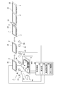
- FIG. 2A is a schematic view of a unit laminate having a four-layer structure.
- FIG. 2B is a schematic view of a unit laminate having a three-layer structure.
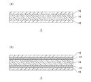
- 3 (A) and 3 (B) are cross-sectional views of the separator.
- FIG. 4A is a schematic view of the infrared irradiation unit and the camera viewed from the second direction.
- FIG. 4B is a schematic view of the infrared irradiation unit and the camera viewed from the first direction.
- FIG. 4A is a schematic view of the infrared irradiation unit and the camera viewed from the second direction.
- FIG. 4B is a schematic view of the infrared irradiation unit and the camera viewed from the first direction.
- FIG. 5A is a schematic view of an infrared irradiation unit and a camera included in the inspection device according to the second embodiment as viewed from a second direction.
- FIG. 5B is a schematic view of the infrared irradiation unit and the camera as viewed from the first direction.
- FIG. 6A is a schematic view of an infrared irradiation unit and a camera included in the inspection device according to the third embodiment as viewed from a second direction.
- FIG. 6B is a schematic view showing an enlarged infrared irradiation surface. It is a schematic diagram of the infrared irradiation part and the camera provided in the inspection apparatus which concerns on Embodiment 4.
- FIG. 5A is a schematic view of an infrared irradiation unit and a camera included in the inspection device according to the second embodiment as viewed from a second direction.
- FIG. 5B is a schematic view of the infrared irradiation unit and
- FIG. 10A is a schematic view of the inspection device according to the first embodiment.
- FIG. 10B is an image obtained by the inspection device according to the first embodiment.
- FIG. 10C is a schematic view of the inspection device according to the second embodiment.
- FIG. 10D is an image obtained by the inspection device according to the second embodiment.
- FIG. 10 (E) is a schematic view of the inspection device according to the third embodiment.
- FIG. 10 (F) is an image obtained by the inspection device according to the third embodiment.
- FIG. 10 (G) is a schematic view of the inspection device according to the fourth embodiment.
- FIG. 10 (H) is an image obtained by the inspection device according to the fourth embodiment.
- FIG. 1 is a schematic view of a production line including a production apparatus for a laminated electrode body according to an embodiment.
- FIG. 2A is a schematic view of a unit laminate having a four-layer structure.
- FIG. 2B is a schematic view of a unit laminate having a three-layer structure. The unit laminate in each figure shows a state in which the separator is seen through.
- 3 (A) and 3 (B) are cross-sectional views of the separator.
- the manufacturing apparatus 1 of the laminated electrode body 100 is an apparatus for manufacturing the laminated electrode body 100 by stacking the unit laminated body 2 (laminated body) on the laminated stage 4.
- the laminated electrode body 100 is composed of, for example, 30 to 40 unit laminated bodies 2.
- the obtained laminated electrode body 100 is used, for example, in a lithium ion secondary battery.
- Examples of the unit laminate 2 include those having a four-layer structure as shown in FIG. 2 (A) and those having a three-layer structure as shown in FIG. 2 (B).
- the unit laminate 2 having a four-layer structure has a structure in which two separators 5 and two electrode plates 7 are laminated and bonded with an adhesive. Specifically, the first separator 6, the first electrode plate 8, the second separator 10, and the second electrode plate 12 are arranged in this order from the top.
- the unit laminate 2 having a three-layer structure has a structure in which two separators 5 and one electrode plate 7 are laminated and bonded with an adhesive. Specifically, the first separator 6, the first electrode plate 8 and the second separator 10 are arranged in this order from the top.
- the first electrode plate 8 is a negative electrode plate
- the second electrode plate 12 is a positive electrode plate.
- first electrode plate 8 and the second electrode plate 12 when it is not necessary to distinguish between the first electrode plate 8 and the second electrode plate 12, they are collectively referred to as an electrode plate 7, and when it is not necessary to distinguish between the first separator 6 and the second separator 10, both are referred to. Are collectively referred to as separator 5.
- the positive electrode plate has a positive electrode current collector and a positive electrode active material layer.
- the positive electrode active material layer is laminated on both sides or one side of the positive electrode current collector. Both the positive electrode current collector and the positive electrode active material layer can be made of a known material, and both have a known structure.
- the positive electrode current collector is composed of, for example, a foil or a porous body made of stainless steel, aluminum, or the like.
- a positive electrode mixture slurry containing a positive electrode active material such as lithium cobalt oxide or lithium iron phosphate, a binder, a dispersant, etc. is applied to the surface of a positive electrode current collector, and the coating film is dried and rolled. It is formed by doing.
- the negative electrode plate has a negative electrode current collector and a negative electrode active material layer.
- the negative electrode active material layer is laminated on both sides or one side of the negative electrode current collector. Both the negative electrode current collector and the negative electrode active material layer can be made of a known material, and both have a known structure.
- the negative electrode current collector is composed of, for example, a foil or a porous body made of copper, aluminum, or the like.
- the negative electrode active material layer is formed by applying a negative electrode mixture slurry containing a negative electrode active material such as graphite, a binder, a dispersant, and the like to the surface of a negative electrode current collector, and drying and rolling the coating film.
- the separator 5 examples include the adhesive separator shown in FIG. 3 (A) and the heat-resistant adhesive separator shown in FIG. 3 (B).
- the adhesive separator is composed of a base material 14 and an adhesive layer 16.
- the base material 14 is a resin sheet made of a polyolefin such as polyethylene (PE) or polypropylene (PP).
- the adhesive layer 16 is made of a polymethyl methacrylate resin (PMMA), a polyvinylidene fluoride resin (PVDF), or the like, and is laminated on the main surfaces on both sides of the base material 14.
- PMMA polymethyl methacrylate resin
- PVDF polyvinylidene fluoride resin
- the adhesive layer 16 may be laminated only on the main surface of one side of the base material 14. Further, the adhesive constituting the adhesive layer 16 may be applied to the entire surface of the main surface of the base material 14, or may be applied locally, for example, in a dot shape.
- the heat-resistant adhesive separator is composed of a base material 14, an adhesive layer 16, and a heat-resistant layer 18.
- the base material 14 and the adhesive layer 16 are as described above.
- the heat-resistant layer 18 is at least a layer having higher heat resistance than the base material 14, and is made of, for example, boehmite, magnesium oxide, barium sulfate, aramid, or the like.
- the heat resistant layer 18 is interposed between the base material 14 and the adhesive layer 16. That is, the heat resistant layer 18 is laminated on the main surface of one side or both sides of the base material 14, and the adhesive layer 16 is laminated on the heat resistant layer 18.
- the first electrode plate 8 is adhered to the adhesive layer 16 of the first separator 6 and the adhesive layer 16 of the second separator 10.
- the second electrode plate 12 is adhered to the adhesive layer 16 of the second separator 10.
- the adhesive layer 16 When the adhesive layer 16 is heated to a predetermined set temperature, it exerts an adhesive force and holds the electrode plate 7. Further, when the adhesive layer 16 in which the electrode plate 7 is adhered is heated to a set temperature or higher, the adhesive force is reduced and the holding of the electrode plate 7 is released. For example, when the temperature of the adhesive layer 16 rises above the glass transition point by heating, the resin constituting the adhesive layer 16 melts and the adhesive strength decreases. Further, the adhesive layer 16 can maintain a state in which the electrode plate 7 is connected to the separator 5 at room temperature (for example, 20 to 25 ° C.).
- the plurality of unit laminated bodies 2 are conveyed in the state of the continuous laminated body 20 connected by the strip-shaped separator continuous body 22.
- the separator continuum 22 is separated into a plurality of unit laminates 2.
- the separator continuum 22 is cut between the electrode plates 7 adjacent to each other in the transport direction of the continuous laminate 20.
- the cut separator continuum 22 becomes the separator 5 in the unit laminated body 2.
- the individualized unit laminate 2 is transported toward the manufacturing apparatus 1 by the transport unit 24.
- the transport unit 24 is composed of a suction head that sucks and holds the unit laminate 2 by, for example, sucking air from a suction hole.
- the position of the unit laminated body 2 with respect to the transport unit 24 is inspected before reaching the manufacturing apparatus 1 of the laminated electrode body 100.
- This position inspection is called the first position inspection.
- the unit laminate 2 is imaged by the camera 28 in a state where the unit laminate 2 is irradiated with light having a predetermined wavelength from the lighting device 26.
- the image captured by the camera 28 is sent to the control device 30.
- the control device 30 has a detection unit 32 that executes a first position inspection.
- the detection unit 32 performs predetermined image processing on the image obtained from the camera 28 to detect the position of the unit laminated body 2 with respect to the transport unit 24.
- the control device 30 is realized by elements and circuits such as a computer CPU and memory as a hardware configuration, and is realized by a computer program or the like as a software configuration, but in FIG. 1, it is realized by their cooperation. It is drawn as a functional block. It is well understood by those skilled in the art that this functional block can be realized in various ways by a combination of hardware and software.
- the unit laminated body 2 subjected to the first position inspection is conveyed to the manufacturing apparatus 1 of the laminated electrode body 100 by the conveying unit 24.
- the manufacturing apparatus 1 of the laminated electrode body 100 includes a laminated stage 4, a transport unit 24, and an inspection device 34.
- the operation of each part of the manufacturing apparatus 1 is controlled by the control apparatus 30. Therefore, the control device 30 can be interpreted as forming a part of the manufacturing device 1.
- the transport unit 24 When the transport unit 24 reaches the stacking position facing the stacking stage 4, it stops sucking air from the suction holes and discharges the unit laminate 2 onto the stacking stage 4.
- the drive of the transport unit 24 is controlled by the transport control unit 36 included in the control device 30.
- the unit laminates 2 are sequentially discharged from the plurality of transport units 24, so that the unit laminates 2 are stacked on the stacking stage 4.
- the stacking stage 4 can be driven in the X-axis direction and the Y-axis direction orthogonal to each other. Further, it can be driven in the Z-axis direction orthogonal to the X-axis direction and the Y-axis direction. Furthermore, it is rotatable around the Z axis.
- the X-axis direction and the Y-axis direction are horizontal directions, and the Z-axis direction is a vertical direction.
- the drive of the laminated stage 4 is controlled by the stage control unit 38 included in the control device 30.
- the stage control unit 38 determines the stacking stage for the unit laminate 2 located directly above the unit laminate 2 based on the position information of the unit laminate 2 obtained in the first position inspection. Adjust the position of 4. As a result, the deviation of the suction position of the unit laminate 2 in the transport unit 24 is corrected, and the unit laminate 2 can be laminated on the lamination stage 4 with high position accuracy.
- the inspection device 34 inspects the position of the electrode plate 7 on the unit laminate 2 from the separator 5 side. In the present embodiment, the position of the first electrode plate 8 is inspected through the first separator 6.
- the inspection device 34 includes an infrared irradiation unit 40, a camera 42, a mirror 44, and a detection unit 32.
- the infrared irradiation unit 40 irradiates the unit laminate 2 with infrared IR (far infrared rays) having a peak wavelength in the range of 6.5 ⁇ m or more and 9.6 ⁇ m or less from the separator 5 side.
- This infrared IR is an electromagnetic wave that passes through the separator 5 (transmits at a predetermined transmittance or higher) but does not pass through the electrode plate 7 (transmits at a predetermined transmittance or less).
- the transmittance of infrared IR with respect to the separator 5 is, for example, 50% or more. Further, the transmittance of infrared IR with respect to the electrode plate 7 is, for example, less than 50%.
- the irradiation time of infrared IR on each unit laminate 2 is, for example, 1 second or less.
- the camera 42 has sensitivity in the wavelength region of infrared IR, and captures infrared IR that passes through the separator 5 and is reflected by the electrode plate 7.
- the camera 42 preferably has a germanium lens at the incident port of the infrared IR. Since the germanium lens has a high transmittance of infrared IR, the electrode plate 7 can be efficiently imaged. Further, since the wavelength of the infrared IR of the present embodiment is 6 ⁇ m or more, a chalcogenide glass lens having a high transmittance as well as a germanium lens can be used.
- FIG. 4A is a schematic view of the infrared irradiation unit 40 and the camera 42 as viewed from the second direction B.
- FIG. 4B is a schematic view of the infrared irradiation unit 40 and the camera 42 as viewed from the first direction A.
- the posture of the infrared irradiation unit 40 of the present embodiment is determined so as to irradiate the infrared IR horizontally. Further, the infrared irradiation unit 40 and the camera 42 are arranged horizontally.
- the direction in which the infrared irradiation unit 40 and the camera 42 are lined up is defined as the first direction A
- the horizontal direction orthogonal to the first direction A is defined as the second direction B
- the vertical direction orthogonal to the first direction A and the second direction B is defined. Is the third direction C.
- the infrared irradiation unit 40 has a heat source 46, a thermocouple 48, a metal plate 50, a mounting bracket 52, and a heat insulating plate 54.
- a heat source 46 a rubber heater or the like can be used.
- the thermocouple 48 controls the output of the heat source 46.
- One of the main surfaces of the metal plate 50 is fixed to the heat source 46 so as to be heat conductive, and the heat generated by the heat source 46 is uniformly propagated.
- the metal plate 50 is made of, for example, a copper plate.
- the other main surface of the metal plate 50 constitutes an infrared irradiation surface 56.
- the infrared irradiation surface 56 is coated with a black body in order to suppress unnecessary radiation and reflection of infrared IR.
- the mounting bracket 52 is provided on the side opposite to the metal plate 50 with the heat source 46 interposed therebetween, and is connected to an external support mechanism.
- the heat insulating plate 54 is composed of, for example, a bake plate, and is arranged between the heat source 46 and the mounting bracket 52. The heat insulating plate 54 suppresses heat transfer from the heat source 46 to the mounting bracket 52 side.
- the camera 42 is arranged between the infrared irradiation unit 40 and the unit laminate 2 on the infrared IR optical path. That is, the camera 42 is arranged in front of the infrared irradiation surface 56 in the infrared IR irradiation direction. Further, the infrared irradiation unit 40 and the camera 42 are arranged so that the infrared irradiation axis of the infrared irradiation unit 40 and the optical axis of the camera 42 extend in parallel.
- the infrared irradiation unit 40 has an infrared irradiation surface 56 that extends outside the camera 42 when viewed from the first direction A in which the camera 42 and the infrared irradiation unit 40 are arranged. Therefore, on the infrared irradiation surface 56, the infrared IR emitted from the region overlapping the camera 42 is hindered by the camera 42 from progressing to the unit laminate 2, but the infrared IR emitted from the region around the camera 42 is. , Can proceed to the unit laminated body 2 side.
- a mirror 44 is arranged on the downstream side of the camera 42 in the optical path of the infrared IR, and the infrared IR is reflected toward the unit laminate 2 by the mirror 44.
- the mirror 44 preferably has a reflective surface coated with gold. As a result, the reflectance of the infrared IR can be increased, and the electrode plate 7 can be efficiently imaged.
- Infrared IR is applied to the unit laminate 2 from the separator 5 side, passes through the separator 5 and reaches the electrode plate 7.
- the infrared IR that has reached the electrode plate 7 is reflected by the electrode plate 7, passes through the separator 5 again, is reflected by the mirror 44, and is incident on the camera 42.
- the unit laminate 2 is imaged by the camera 42. If the posture of the infrared irradiation unit 40 is determined so that the unit laminate 2 can be directly irradiated with the infrared IR, the mirror 44 can be omitted.
- the camera 42 sends the captured image information to the detection unit 32.
- the detection unit 32 detects the position of the electrode plate 7 based on the image captured by the camera 42. This position inspection is called a second position inspection. Regarding the second position inspection, the detection unit 32 holds in advance the reference position information of the electrode plate 7 and the threshold value of the amount of deviation from the reference position.
- the reference position information is, for example, the position information of two predetermined corners of the electrode plate 7.
- the detection unit 32 collates the positions of the two corners in the image with the reference positions. Then, when the amount of deviation between the two angles with respect to the reference position is larger than the threshold value, the detection unit 32 determines that the stacking position of the unit laminated body 2 is incompatible.
- the detection unit 32 sends this determination result to the transport control unit 36.
- the transfer control unit 36 controls the transfer unit 24 so as to suck the unit laminate 2 determined to be non-conforming again and remove it from the stacking stage 4. Then, the transfer control unit 36 controls the transfer unit 24 so that the removed unit laminated body 2 is laminated again or discharged out of the line.
- the detection unit 32 executes both the first position inspection and the second position inspection, but the first position inspection and the second position inspection may be executed by separate detection units. Further, the detection unit 32 that executes the second position inspection may be independent of the control device 30 that controls each unit of the manufacturing device 1. Further, the infrared irradiation unit 40 and the camera 42 may be used for the first position inspection.
- the temperature rise of the unit laminate 2 due to the irradiation of the infrared IR can be suppressed to 50 ° C. or less, more preferably 40 ° C. or less.
- the electrode plate 7 can be imaged through the separator 5 while suppressing the decrease in the adhesive force of the adhesive layer 16.
- the inspection device 34 is an device that inspects the position of the electrode plate 7 in the laminated body of the separator 5 and the electrode plate 7 from the separator 5 side, and has a peak wavelength of 6.5 ⁇ m or more.
- the infrared irradiation unit 40 that irradiates the unit laminate 2 with infrared IR in the range of 9.6 ⁇ m or less from the separator 5 side, and the infrared IR wavelength region that has sensitivity, passes through the separator 5 and is reflected by the electrode plate 7.
- a camera 42 that captures infrared IR and a detection unit 32 that detects the position of the electrode plate 7 based on the image captured by the camera 42 are provided.
- the manufacturing apparatus 1 of the laminated electrode body 100 conveys the laminated body 4 on which the unit laminated body 2 to which the separator 5 and the electrode plate 7 are adhered with an adhesive is stacked, and the unit laminated body 2.
- a transport unit 24 that is discharged onto the stacking stage 4 and an inspection device 34 that inspects the position of the electrode plate 7 on the unit laminate 2 discharged from the transport unit 24 are provided.
- the camera 42 is arranged between the infrared irradiation unit 40 and the unit laminate 2 on the optical path of the infrared IR.
- the infrared irradiation unit 40 has an infrared irradiation surface 56 extending to the outside of the camera 42 when viewed from the first direction A in which the camera 42 and the infrared irradiation unit 40 are arranged.
- FIG. 5A is a schematic view of the infrared irradiation unit 40 and the camera 42 included in the inspection device 34 according to the second embodiment as viewed from the second direction B.
- FIG. 5B is a schematic view of the infrared irradiation unit 40 and the camera 42 as viewed from the first direction A.
- the infrared irradiation unit 40 of the present embodiment has a heat source 46, a thermocouple 48, a metal plate 50, a mounting bracket 52, a heat insulating plate 54, and the same as the infrared irradiation unit 40 described in the first embodiment. It has an infrared irradiation surface 56. Further, the infrared irradiation surface 56 has a through hole 58. In the present embodiment, the through hole 58 penetrates the entire infrared irradiation portion 40 in the first direction A from the infrared irradiation surface 56 to the heat insulating plate 54.
- the infrared irradiation unit 40 and the camera 42 are arranged so that the through hole 58 and the optical axis O of the camera 42 overlap each other when viewed from the first direction A in which the infrared irradiation unit 40 and the camera 42 are arranged.
- the camera 42 may be arranged on the back side of the infrared irradiation unit 40, the infrared irradiation unit 40 may be arranged on the back side of the camera 42, or at least a part of the camera 42 may be arranged in the through hole 58. It may be arranged.
- the infrared irradiation unit 40 When the infrared irradiation unit 40 is arranged on the back side of the camera 42, by overlapping the through hole 58 and the optical axis O, the amount of infrared IR whose progress is hindered by the camera 42 can be reduced, and the infrared IR can be reduced. It is possible to improve the utilization efficiency of.
- FIG. 6A is a schematic view of the infrared irradiation unit 40 and the camera 42 included in the inspection device 34 according to the third embodiment as viewed from the second direction B.
- FIG. 6B is an enlarged schematic view showing the infrared irradiation surface 56.
- the infrared irradiation unit 40 of the present embodiment has a heat source 46, a thermocouple 48, a metal plate 50, a mounting bracket 52, a heat insulating plate 54, and the same as the infrared irradiation unit 40 described in the first embodiment. It has an infrared irradiation surface 56. Further, similarly to the infrared irradiation surface 56 described in the second embodiment, the infrared irradiation surface 56 has a through hole 58. The through hole 58 penetrates the entire infrared irradiation portion 40 in the first direction A from the infrared irradiation surface 56 to the heat insulating plate 54.
- the infrared irradiation unit 40 and the camera 42 are arranged so that the through hole 58 and the optical axis O of the camera 42 overlap each other when viewed from the first direction A in which the infrared irradiation unit 40 and the camera 42 are arranged.
- the infrared irradiation surface 56 included in the infrared irradiation unit 40 of the present embodiment includes a first irradiation region 56a and a second irradiation region 56b.
- first irradiation region 56a infrared IR is incident on the unit laminated body 2 at a predetermined first incident angle ⁇ 1.
- second irradiation region 56b infrared IR is incident on the unit laminated body 2 at a second incident angle ⁇ 2 different from the first incident angle ⁇ 1.
- the infrared irradiation unit 40 has a parabolic shape (parabolic shape) infrared irradiation surface 56.
- the infrared irradiation unit 40 is preferably arranged so that the focal point of the paraboloid is located in the vicinity of the unit laminate 2 or overlaps with the unit laminate 2.
- the infrared IR emitted from the first irradiation region 56a located outside the infrared irradiation surface 56 is incident on the unit laminate 2 at a predetermined first incident angle ⁇ 1.
- the infrared IR emitted from the second irradiation region 56b located on the center side of the infrared irradiation surface 56 with respect to the first irradiation region 56a has a second incident angle ⁇ 2 smaller than the first incident angle ⁇ 1 and the unit laminate 2 Is incident on.
- the infrared IR emitted from the infrared irradiation surface 56 incident on the unit laminate 2 at a plurality of incident angles it is possible to improve the incident efficiency of the infrared IR reflected by the electrode plate 7 on the camera 42. It is possible to obtain a higher contrast image. As a result, the position of the electrode plate 7 can be inspected with higher accuracy.
- the contrast of the image is increased by injecting infrared IR into the unit laminate 2 at a plurality of incident angles, and the contrast of the image is increased by overlapping the through hole 58 and the optical axis O when viewed from the first direction A. Can be implemented independently of each other.
- the fourth embodiment has the same configuration as the first embodiment except for the arrangement of the infrared irradiation unit 40 and the camera 42.
- the present embodiment will be mainly described with a configuration different from that of the first embodiment, and the common configuration will be briefly described or the description will be omitted.
- FIG. 7 is a schematic view of the infrared irradiation unit 40 and the camera 42 included in the inspection device 34 according to the fourth embodiment.
- the infrared irradiation unit 40 of the present embodiment has a heat source 46, a thermocouple 48, a metal plate 50, a mounting bracket 52, a heat insulating plate 54, and the same as the infrared irradiation unit 40 described in the first embodiment. It has an infrared irradiation surface 56. Further, the infrared irradiation surface 56 of the present embodiment has a central axis P inclined with respect to the normal line n of the unit laminate 2.
- the central axis P is, for example, a virtual straight line extending from the geometric center of the contour shape of the infrared irradiation surface 56 seen from the unit laminated body 2 side to the unit laminated body 2 side.
- the camera 42 is arranged so that the optical axis O is tilted with respect to the normal line n of the unit laminated body 2.
- the central axis P of the infrared irradiation surface 56 is tilted by an angle ⁇ 3 from the normal line n.
- the optical axis O of the camera 42 is tilted by an angle ⁇ 4 from the normal line n.
- the angle ⁇ 3 and the angle ⁇ 4 may be the same or different.
- the central axis P and the optical axis O are inclined in opposite directions with respect to the normal line n. That is, the direction in which the central axis P is tilted and the direction in which the optical axis O is tilted are deviated by 180 ° around the normal line n.
- the infrared irradiation surface 56 and the camera 42 in this way, it is possible to increase the incident efficiency of the infrared IR reflected by the electrode plate 7 on the camera 42, and it is possible to obtain a higher contrast image. As a result, the position of the electrode plate 7 can be inspected with higher accuracy.
- the laminated body (2) is irradiated with infrared rays (IR) having a peak wavelength in the range of 6.5 ⁇ m or more and 9.6 ⁇ m or less from the separator (5) side.
- IR infrared ray
- An infrared ray (IR) transmitted through the separator (5) and reflected by the electrode plate (7) is imaged by a camera (42) having sensitivity in the wavelength region of the infrared ray (IR). Includes detecting the position of the electrode plate (7) based on the image captured by the camera (42). Inspection method.
- Verification test I Verification of infrared wavelength range
- FIG. 8 is a schematic view of the inspection device 34 used in the verification test I.
- the camera 42 was placed directly above the unit laminate 2.
- the camera 42 includes an image sensor 42a and a condenser lens 60.
- the condenser lens 60 is arranged between the unit laminate 2 and the image pickup device 42a.
- the infrared irradiation unit 40 is arranged so as to irradiate the unit laminate 2 with infrared IR diagonally.
- the structure of the infrared irradiation unit 40 is the same as that of the infrared irradiation unit 40 included in the inspection device 34 of the first embodiment (see FIG. 4A).
- each separator 5 includes a base material 14 made of PE, a heat resistant layer 18 made of magnesium oxide and laminated on both sides of the base material 14, and an adhesive layer 16 made of PVDF and laminated on each heat resistant layer 18.
- Each separator 5 and the first electrode plate 8 were heated to 50 ° C. and pressure-bonded.
- infrared IRs having various peak wavelengths were irradiated to the unit laminate 2 for 1 second from the infrared irradiation unit 40, and the unit laminate 2 was imaged by the camera 42.
- the infrared IR that has reached the unit laminate 2 passes through the first separator 6 and is reflected by the first electrode plate 8.
- the infrared IR reflected by the first electrode plate 8 passes through the condenser lens 60 and is imaged on the image sensor 42a.
- the peak wavelengths of infrared IR were 6.5 ⁇ m, 8.7 ⁇ m, 8.9 ⁇ m, 9.0 ⁇ m, 9.2 ⁇ m, 9.3 ⁇ m, and 9.6 ⁇ m.
- the surface temperature of the unit laminate 2 after 1 second after irradiation with infrared IR was measured with a contact thermometer.
- the temperature of the infrared irradiation surface 56 was measured by attaching a thermocouple to the surface of the infrared irradiation surface 56 and using a digital thermometer.
- changes in the state of the unit laminate 2 including peeling of the separator were visually confirmed.
- FIG. 9 is a diagram showing the results of verification test I. As shown in FIG. 9, it was confirmed that when the unit laminate 2 was irradiated with infrared IR having a peak wavelength of 6.5 ⁇ m to 9.6 ⁇ m, the position of the first electrode plate 8 could be inspected from the first separator 6 side. The surface temperature of the unit laminate 2 was 28.0 ° C. or lower, which was sufficiently lower than the bonding temperature of the adhesive layer 16 of 50 ° C. As a matter of course, no peeling of the separator 5 was observed at any of the peak wavelengths.
- the present inventor visually confirmed that the separator peels off when the peak wavelength of infrared IR is less than 6.5 ⁇ m or more than 9.6 ⁇ m.
- the peak wavelength of the infrared IR is less than 6.5 ⁇ m
- the adhesive strength of the adhesive layer 16 decreases due to the temperature rise of the separator 5 due to the irradiation of the infrared IR. Since the surface temperature of the separator 5 tends to rise as the wavelength of the infrared IR is shorter, the separator 5 is likely to be peeled off when the peak wavelength is less than 6.5 ⁇ m.
- the peak wavelength of the infrared IR exceeds 9.6 ⁇ m
- the temperature rise of the separator 5 is suppressed.
- the electrode plate 7 is heated by irradiation with infrared IR, and the adhesive strength of the adhesive layer 16 decreases due to the temperature rise of the electrode plate 7.
- the infrared IR reaches the electrode plate 7
- the electrons in the metal constituting the electrode plate 7 vibrate and generate heat.
- the temperature of the electrode plate 7 rises.
- the electrode plate 7 is covered with the separator 5, heat tends to be accumulated in the electrode plate 7, and the temperature of the electrode plate 7 rises in a relatively short time. Since the temperature of the electrode plate 7 tends to rise as the wavelength of the infrared IR becomes longer, the separator 5 tends to peel off when the peak wavelength exceeds 9.6 ⁇ m.
- Verification test II Verification of infrared irradiation part and camera
- the verification test II verified the influence of the shape of the infrared irradiation unit and the arrangement of the infrared irradiation unit and the camera on the image pickup of the camera.
- FIG. 10A is a schematic view of the inspection device 34 according to the first embodiment.
- FIG. 10B is an image obtained by the inspection device 34 according to the first embodiment.
- the inspection device 34 of the first embodiment is the same as the inspection device 34 used in the verification test I (see FIG. 8).
- FIG. 10C is a schematic view of the inspection device 34 according to the second embodiment.
- FIG. 10D is an image obtained by the inspection device 34 according to the second embodiment.
- the inspection device 34 of the second embodiment is the same as the inspection device 34 described in the first embodiment (see FIG. 4A).
- FIG. 10 (E) is a schematic view of the inspection device 34 according to the third embodiment.
- FIG. 10 (F) is an image obtained by the inspection device 34 according to the third embodiment.
- the inspection device 34 of the third embodiment is the same as the inspection device 34 described in the fourth embodiment (see FIG. 7).
- FIG. 10 (G) is a schematic view of the inspection device 34 according to the fourth embodiment.
- FIG. 10 (H) is an image obtained by the inspection device 34 according to the fourth embodiment.
- the inspection device 34 of the fourth embodiment is the same as the inspection device 34 described in the third embodiment (see FIG. 6A).
- the same unit laminate 2 as in the evaluation test I was used. Under the condition of room temperature of 26 ° C., the unit laminate 2 was irradiated with infrared IR having a peak wavelength of 9.35 ⁇ m from the infrared irradiation unit 40 for 1 second, and the unit laminate 2 was imaged by the camera 42.
- the image shown in FIG. 10B was obtained by the inspection device 34 of the first embodiment in which the camera 42 was arranged directly above the unit laminated body 2 and the infrared IR was irradiated obliquely.
- the inspection device 34 of the second embodiment in which the camera 42 is arranged between the infrared irradiation unit 40 and the unit laminate 2, as shown in FIG. 10D, the inspection device 34 of the first embodiment is more than the inspection device 34 of the first embodiment. A high-contrast image was obtained. This makes it possible to more clearly distinguish between the separator 5 and the electrode plate 7.
- the inspection device 34 according to the second embodiment that is, the inspection device 34 in which the through hole 58 provided in the infrared irradiation surface 56 and the optical axis O of the camera 42 are overlapped with each other is also used in the second embodiment. It is presumed that an image having a high contrast equal to or higher than that of the inspection device 34 of the above can be obtained.
- the inspections of the first and second embodiments are performed. An image with higher contrast was obtained as compared with the device 34. Further, in the inspection device 34 of the fourth embodiment having the parabolic-shaped infrared irradiation surface 56, as shown in FIG. 10 (H), an image having a high contrast equal to or higher than that of the inspection device 34 of the third embodiment can be obtained. rice field.
- the contrast of the image can be enhanced by irradiating the infrared IR from the back surface of the camera 42 and by superimposing the through hole 58 provided on the infrared irradiation surface 56 and the optical axis O of the camera 42. .. Further, it was confirmed that the contrast of the image can be enhanced by inclining the central axis P of the infrared irradiation surface 56 and the optical axis O of the camera 42 with respect to the normal line n of the unit laminate 2.
- the present disclosure can be used for an inspection device, a manufacturing device for a laminated electrode body, and an inspection method.
Landscapes
- Chemical & Material Sciences (AREA)
- Chemical Kinetics & Catalysis (AREA)
- Electrochemistry (AREA)
- General Chemical & Material Sciences (AREA)
- Engineering & Computer Science (AREA)
- Manufacturing & Machinery (AREA)
- Physics & Mathematics (AREA)
- General Physics & Mathematics (AREA)
- Investigating Materials By The Use Of Optical Means Adapted For Particular Applications (AREA)
- Secondary Cells (AREA)
Abstract
検査装置34は、セパレータ5および電極板7が接着剤で接着された積層体における電極板7の位置をセパレータ5側から検査する装置である。検査装置34は、ピーク波長が6.5μm以上9.6μm以下の範囲にある赤外線IRをセパレータ5側から積層体に照射する赤外線照射部40と、赤外線IRの波長領域に感度を有し、セパレータ5を透過し電極板7で反射される赤外線IRを撮像するカメラ42と、カメラ42により撮像された画像に基づいて電極板7の位置を検出する検出部32と、を備える。
Description
本開示は、検査装置、積層電極体の製造装置および検査方法に関する。
近年、電気自動車(EV)、ハイブリッド車(HV)、プラグインハイブリッド車(PHV)等の普及にともない、車載用の二次電池の出荷が増えている。特にリチウムイオン二次電池の出荷が増えている。また、車載用に限らず、例えばノート型パソコン等の携帯端末用の電源としても二次電池の普及が進んでいる。このような二次電池としては、積層タイプの電池が知られている。一般に積層タイプの電池は、複数の正極板と複数の負極板とがセパレータを挟んで交互に積層された積層電極体が、電解液ととともに外装缶に収容された構造を有する。
積層電極体の形成方法としては、2枚の電極板と2枚のセパレータとで構成される単位積層体を順に積層していく方法がある。単位積層体は、電極板とセパレータとが交互に積層され、接着剤で4層が接着された構造を有する。この方法では、単位積層体を順次積層していく際に、各電極板のずれを極力なくすことが求められる。各電極板のずれは、二次電池の性能向上を妨げ得るためである。例えば、正極板が負極板の外にはみ出した場合、充放電の繰り返しによってリチウムが析出して、短絡等の電気的不良が発生し得る。
したがって、単位積層体の積層工程において、積層した単位積層体における電極板の位置を検査することが望まれる。これに対し特許文献1には、袋状に形成されたセパレータ内に配置された電極に対して、セパレータを透過し電極を透過しない赤外線を投射し、電極が反射した赤外線をカメラで受光して電極の位置を検出する電極位置検出装置が開示されている。
従来の検出装置では、単位積層体に照射する赤外線の熱によって接着剤の接着力が低下するおそれがあった。接着剤の接着力が低下すると、セパレータが剥がれて電極板が露出したり、セパレータや電極板に皺が生じたりするおそれがある。当該露出や皺の発生は、短絡や電解液の含浸むら等の不良を引き起こし得る。
本開示はこうした状況に鑑みてなされたものであり、その目的の1つは、セパレータおよび電極板の接着強度の低下を抑制しながら電極板の位置を検出する技術を提供することにある。
本開示のある態様は、セパレータおよび電極板が接着剤で接着された積層体における電極板の位置をセパレータ側から検査する検査装置である。この検査装置は、ピーク波長が6.5μm以上9.6μm以下の範囲にある赤外線をセパレータ側から積層体に照射する赤外線照射部と、赤外線の波長領域に感度を有し、セパレータを透過し電極板で反射される赤外線を撮像するカメラと、カメラにより撮像された画像に基づいて電極板の位置を検出する検出部と、を備える。
本開示の他の態様は、積層電極体の製造装置である。この製造装置は、セパレータおよび電極板が接着剤で接着された積層体が積み重ねられる積層ステージと、積層体を搬送して積層ステージ上に放出する搬送部と、搬送部から放出された積層体における電極板の位置を検査する上記態様の検査装置と、を備え、積層体を積み重ねて積層電極体を製造する。
本開示の他の態様は、セパレータおよび電極板が接着剤で接着された積層体における電極板の位置をセパレータ側から検査する検査方法である。この検査方法は、ピーク波長が6.5μm以上9.6μm以下の範囲にある赤外線をセパレータ側から積層体に照射し、赤外線の波長領域に感度を有するカメラによって、セパレータを透過し電極板で反射される赤外線を撮像し、カメラにより撮像された画像に基づいて電極板の位置を検出することを含む。
以上の構成要素の任意の組合せ、本開示の表現を方法、装置、システムなどの間で変換したものもまた、本開示の態様として有効である。
本開示によれば、セパレータおよび電極板の接着強度の低下を抑制しながら電極板の位置を検出することができる。
以下、本開示を好適な実施の形態をもとに図面を参照しながら説明する。実施の形態は、本開示を限定するものではなく例示であって、実施の形態に記述されるすべての特徴やその組み合わせは、必ずしも本開示の本質的なものであるとは限らない。各図面に示される同一または同等の構成要素、部材、処理には、同一の符号を付するものとし、適宜重複した説明は省略する。また、各図に示す各部の縮尺や形状は、説明を容易にするために便宜的に設定されており、特に言及がない限り限定的に解釈されるものではない。また、本明細書または請求項中に「第1」、「第2」等の用語が用いられる場合には、特に言及がない限りこの用語はいかなる順序や重要度を表すものでもなく、ある構成と他の構成とを区別するためのものである。また、各図面において実施の形態を説明する上で重要ではない部材の一部は省略して表示する。
(実施の形態1)
図1は、実施の形態に係る積層電極体の製造装置を含む製造ラインの模式図である。図2(A)は、4層構造を有する単位積層体の模式図である。図2(B)は、3層構造を有する単位積層体の模式図である。各図における単位積層体は、セパレータを透視した状態を図示している。図3(A)および図3(B)は、セパレータの断面図である。
図1は、実施の形態に係る積層電極体の製造装置を含む製造ラインの模式図である。図2(A)は、4層構造を有する単位積層体の模式図である。図2(B)は、3層構造を有する単位積層体の模式図である。各図における単位積層体は、セパレータを透視した状態を図示している。図3(A)および図3(B)は、セパレータの断面図である。
積層電極体100の製造装置1は、単位積層体2(積層体)を積層ステージ4上に積み重ねて積層電極体100を製造する装置である。積層電極体100は、例えば30~40枚の単位積層体2で構成される。得られた積層電極体100は、例えばリチウムイオン二次電池に用いられる。単位積層体2としては、図2(A)に示すように4層構造を有するものと、図2(B)に示すように3層構造を有するものとが例示される。
4層構造の単位積層体2は、2枚のセパレータ5と2枚の電極板7とが積層され、接着剤で接着された構造を有する。具体的には、第1セパレータ6、第1極板8、第2セパレータ10および第2極板12が上からこの順に並ぶ。3層構造の単位積層体2は、2枚のセパレータ5と1枚の電極板7とが積層され、接着剤で接着された構造を有する。具体的には、第1セパレータ6、第1極板8および第2セパレータ10が上からこの順に並ぶ。本実施の形態では、第1極板8は負極板であり、第2極板12は正極板である。以下では、第1極板8および第2極板12を区別する必要がない場合は両者をまとめて電極板7と称し、第1セパレータ6および第2セパレータ10を区別する必要がない場合は両者をまとめてセパレータ5と称する。
正極板は、正極集電体および正極活物質層を有する。正極活物質層は、正極集電体の両面または片面に積層される。正極集電体および正極活物質層は、いずれも公知の材料で構成することができ、いずれも公知の構造を有する。正極集電体は、例えば、ステンレス鋼やアルミニウム等からなる箔や多孔体で構成される。正極活物質層は、コバルト酸リチウムやリン酸鉄リチウム等の正極活物質、結着材および分散剤等を含む正極合材スラリーを正極集電体の表面に塗布し、塗膜を乾燥、圧延することで形成される。
負極板は、負極集電体および負極活物質層を有する。負極活物質層は、負極集電体の両面または片面に積層される。負極集電体および負極活物質層は、いずれも公知の材料で構成することができ、いずれも公知の構造を有する。負極集電体は、例えば、銅やアルミニウム等からなる箔や多孔体で構成される。負極活物質層は、黒鉛等の負極活物質、結着材および分散剤等を含む負極合材スラリーを負極集電体の表面に塗布し、塗膜を乾燥、圧延することで形成される。
セパレータ5としては、図3(A)に示す接着セパレータと、図3(B)に示す耐熱性接着セパレータとが例示される。接着セパレータは、基材14と、接着剤層16と、で構成される。基材14は、例えばポリエチレン(PE)、ポリプロピレン(PP)等のポリオレフィンからなる樹脂シートである。接着剤層16は、ポリメタクリル酸メチル樹脂(PMMA)、ポリフッ化ビニリデン樹脂(PVDF)等からなり、基材14の両側の主表面に積層される。なお、接着剤層16は、基材14の片側の主表面のみに積層されてもよい。また、接着剤層16を構成する接着剤は、基材14の主表面の全面に塗布されてもよいし、局所的、例えばドット状に塗布されてもよい。
耐熱性接着セパレータは、基材14と、接着剤層16と、耐熱剤層18と、で構成される。基材14および接着剤層16は、上述のとおりである。耐熱剤層18は、少なくとも基材14よりも耐熱性の高い層であり、例えばベーマイト、酸化マグネシウム、硫酸バリウム、アラミド等からなる。耐熱剤層18は、基材14と接着剤層16との間に介在する。つまり、基材14の片側または両側の主表面に耐熱剤層18が積層され、耐熱剤層18の上に接着剤層16が積層される。
第1極板8は、第1セパレータ6の接着剤層16と、第2セパレータ10の接着剤層16とに接着される。第2極板12は、第2セパレータ10の接着剤層16に接着される。接着剤層16は、所定の設定温度まで加熱すると接着力を発揮し、電極板7を保持する。また、電極板7が接着した状態にある接着剤層16を設定温度以上まで加熱すると、接着力が低下して電極板7の保持が解除される。例えば、接着剤層16は、加熱によりガラス転移点以上の温度まで上昇すると、接着剤層16を構成する樹脂が溶融して接着力が低下する。また、接着剤層16は、室温(例えば20~25℃)では電極板7がセパレータ5に連結された状態を維持することができる。
積層電極体100の製造ラインにおいて、複数の単位積層体2は、帯状のセパレータ連続体22でつながれた連続積層体20の状態で搬送される。カッター23によってセパレータ連続体22が切断されることで、複数の単位積層体2に個片化される。このとき、セパレータ連続体22は、連続積層体20の搬送方向で隣り合う電極板7の間において切断される。切断されたセパレータ連続体22は、単位積層体2においてセパレータ5となる。個片化された単位積層体2は、搬送部24によって製造装置1に向けて搬送される。搬送部24は、例えば吸着穴からの空気の吸引によって単位積層体2を吸着保持する吸着ヘッドで構成される。
単位積層体2は、積層電極体100の製造装置1に至る前に、搬送部24に対する位置が検査される。この位置検査を第1位置検査という。第1位置検査では、照明装置26から所定波長の光が単位積層体2に照射された状態で、カメラ28によって単位積層体2が撮像される。カメラ28によって撮像された画像は、制御装置30に送られる。制御装置30は、第1位置検査を実行する検出部32を有する。検出部32は、カメラ28から得られた画像に所定の画像処理を施して、搬送部24に対する単位積層体2の位置を検出する。
制御装置30は、ハードウェア構成としてはコンピュータのCPUやメモリをはじめとする素子や回路で実現され、ソフトウェア構成としてはコンピュータプログラム等によって実現されるが、図1では、それらの連携によって実現される機能ブロックとして描いている。この機能ブロックがハードウェアおよびソフトウェアの組合せによっていろいろなかたちで実現できることは、当業者には当然に理解されるところである。
第1位置検査が施された単位積層体2は、搬送部24によって積層電極体100の製造装置1に搬送される。積層電極体100の製造装置1は、積層ステージ4と、搬送部24と、検査装置34と、を備える。製造装置1の各部の動作は、制御装置30によって制御される。したがって、制御装置30は、製造装置1の一部を構成すると解釈され得る。
搬送部24は、積層ステージ4と対向する積層位置に到達すると、吸着穴からの空気の吸引を停止して、単位積層体2を積層ステージ4上に放出する。搬送部24の駆動は、制御装置30が有する搬送制御部36によって制御される。複数の搬送部24から単位積層体2が順次放出されることで、積層ステージ4上に単位積層体2が積み重ねられていく。
積層ステージ4は、互いに直交するX軸方向およびY軸方向に駆動可能である。また、X軸方向およびY軸方向と直交するZ軸方向に駆動可能である。さらに、Z軸周りに回動可能である。X軸方向およびY軸方向は水平方向であり、Z軸方向は鉛直方向である。積層ステージ4の駆動は、制御装置30が有するステージ制御部38によって制御される。搬送部24から単位積層体2が放出される際、ステージ制御部38は、第1位置検査で得られた単位積層体2の位置情報に基づいて、直上に位置する単位積層体2に対する積層ステージ4の位置を調整する。これにより、搬送部24における単位積層体2の吸着位置のずれが補正されて、積層ステージ4上に高い位置精度で単位積層体2を積層することができる。
搬送部24から積層ステージ4に単位積層体2が放出されると、積層ステージ4に載置された単位積層体2の位置が検査装置34によって検査される。検査装置34は、単位積層体2における電極板7の位置をセパレータ5側から検査する。本実施の形態では、第1極板8の位置を第1セパレータ6越しに検査する。
検査装置34は、赤外線照射部40と、カメラ42と、ミラー44と、検出部32と、を備える。赤外線照射部40は、ピーク波長が6.5μm以上9.6μm以下の範囲にある赤外線IR(遠赤外線)をセパレータ5側から単位積層体2に照射する。この赤外線IRは、セパレータ5を透過する(所定の透過率以上で透過する)が、電極板7を透過しない(所定の透過率未満で透過する)電磁波である。セパレータ5に対する赤外線IRの透過率は、例えば50%以上である。また、電極板7に対する赤外線IRの透過率は、例えば50%未満である。各単位積層体2に対する赤外線IRの照射時間は、例えば1秒以下である。
カメラ42は、赤外線IRの波長領域に感度を有し、セパレータ5を透過し電極板7で反射される赤外線IRを撮像する。カメラ42は、好ましくは赤外線IRの入射口にゲルマニウムレンズを有する。ゲルマニウムレンズは、赤外線IRの透過率が高いため、電極板7を効率よく撮像することができる。また、本実施の形態の赤外線IRの波長は6μm以上であるため、ゲルマニウムレンズと同様に高い透過率を持つカルコゲナイドガラスレンズも使用できる。
図4(A)は、第2方向Bから見た赤外線照射部40およびカメラ42の模式図である。図4(B)は、第1方向Aから見た赤外線照射部40およびカメラ42の模式図である。本実施の形態の赤外線照射部40は、水平に赤外線IRを照射するように姿勢が定められている。また、赤外線照射部40とカメラ42とは、水平に配列されている。以下、赤外線照射部40とカメラ42とが並ぶ方向を第1方向Aとし、第1方向Aと直交する水平方向を第2方向Bとし、第1方向Aおよび第2方向Bと直交する鉛直方向を第3方向Cとする。
赤外線照射部40は、熱源46と、熱電対48と、金属板50と、取付ブラケット52と、断熱板54と、を有する。熱源46としては、ラバーヒータ等を用いることができる。熱電対48は、熱源46の出力を制御する。金属板50は、一方の主表面が熱源46に熱伝導可能に固定され、熱源46が発生させた熱を均一に伝搬する。金属板50は、例えば銅板で構成される。金属板50の他方の主表面は、赤外線照射面56を構成する。赤外線照射面56には、赤外線IRの不要な輻射や反射を抑制するために黒体塗装が施されている。
取付ブラケット52は、熱源46を挟んで金属板50とは反対側に設けられ、外部の支持機構に接続される。断熱板54は、例えばベーク板で構成され、熱源46と取付ブラケット52との間に配置される。断熱板54により、熱源46から取付ブラケット52側への伝熱が抑制される。
カメラ42は、赤外線IRの光路上で赤外線照射部40と単位積層体2との間に配置される。つまり、カメラ42は、赤外線IRの照射方向で赤外線照射面56の前方に配置される。また、赤外線照射部40とカメラ42とは、赤外線照射部40の赤外線照射軸とカメラ42の光軸とが平行に延びるように配置される。赤外線照射部40は、カメラ42と赤外線照射部40とが並ぶ第1方向Aから見て、カメラ42の外側に広がる赤外線照射面56を有する。このため、赤外線照射面56において、カメラ42と重なる領域から照射される赤外線IRはカメラ42によって単位積層体2への進行が阻害されるが、カメラ42の周囲の領域から照射される赤外線IRは、単位積層体2側に進行することができる。
赤外線IRの光路におけるカメラ42よりも下流側にはミラー44が配置され、ミラー44によって赤外線IRが単位積層体2に向けて反射される。これにより、赤外線照射部40から水平方向に照射された赤外線IRが、積層ステージ4に載置された単位積層体2に向かって進行する。ミラー44は、好ましくは反射面に金がコーティングされる。これにより、赤外線IRの反射率を高めて、電極板7を効率よく撮像することができる。
赤外線IRは、セパレータ5側から単位積層体2に照射され、セパレータ5を透過して電極板7に到達する。電極板7に到達した赤外線IRは、電極板7で反射されて再びセパレータ5を透過し、ミラー44で反射されてカメラ42に入射する。これにより、カメラ42によって単位積層体2が撮像される。なお、赤外線照射部40が単位積層体2に直に赤外線IRを照射可能に姿勢が定められる場合には、ミラー44を省略することができる。
カメラ42は、撮像した画像情報を検出部32に送る。検出部32は、カメラ42により撮像された画像に基づいて電極板7の位置を検出する。この位置検査を第2位置検査という。第2位置検査に関して、検出部32は、電極板7の基準位置情報と、基準位置からのずれ量のしきい値と、を予め保持している。基準位置情報は、例えば電極板7の所定の2つの角部の位置情報である。検出部32は、カメラ42から画像を取得すると、画像における2つの角部の位置を基準位置と照合する。そして、基準位置に対する2つの角度のずれ量がしきい値よりも大きい場合、検出部32は、単位積層体2の積層位置が不適合であると判断する。
検出部32は、この判断結果を搬送制御部36に送る。搬送制御部36は、検出部32から判断結果を受領すると、不適合と判断された単位積層体2を再び吸引して積層ステージ4上から取り除くように搬送部24を制御する。そして、搬送制御部36は、取り除いた単位積層体2を再び積層するか、ライン外に排出するように搬送部24を制御する。
本実施の形態では、検出部32が第1位置検査および第2位置検査の両方を実行しているが、第1位置検査と第2位置検査とは別々の検出部によって実行されてもよい。また、第2位置検査を実行する検出部32は、製造装置1の各部を制御する制御装置30とは独立していてもよい。また、赤外線照射部40およびカメラ42は、第1位置検査に用いられてもよい。
赤外線IRのピーク波長の範囲を6.5μm~9.6μmにすることで、赤外線IRの照射による単位積層体2の温度上昇を50℃以下、より好ましくは40℃以下に抑えることができる。これにより、接着剤層16の接着力の低下を抑えながら、セパレータ5越しに電極板7を撮像することができる。
以上説明したように、本実施の形態に係る検査装置34は、セパレータ5および電極板7の積層体における電極板7の位置をセパレータ5側から検査する装置であり、ピーク波長が6.5μm以上9.6μm以下の範囲にある赤外線IRをセパレータ5側から単位積層体2に照射する赤外線照射部40と、赤外線IRの波長領域に感度を有し、セパレータ5を透過し電極板7で反射される赤外線IRを撮像するカメラ42と、カメラ42により撮像された画像に基づいて電極板7の位置を検出する検出部32と、を備える。
このように、特定の波長の赤外線IRを単位積層体2に照射して電極板7の位置を検出することで、接着剤層16が接着力の低下する温度まで上昇することを抑制できる。これにより、セパレータ5と電極板7との接着状態を保ちながら、セパレータ5越しに電極板7の位置を検査することができる。
また、本実施の形態に係る積層電極体100の製造装置1は、セパレータ5および電極板7が接着剤で接着された単位積層体2が積み重ねられる積層ステージ4と、単位積層体2を搬送して積層ステージ4上に放出する搬送部24と、搬送部24から放出された単位積層体2における電極板7の位置を検査する検査装置34と、を備える。これにより、積層電極体100の品質向上を図ることができ、二次電池の大容量化と安全性との両立を図ることができる。
また、本実施の形態の検査装置34では、カメラ42が赤外線IRの光路上で赤外線照射部40と単位積層体2との間に配置される。また、赤外線照射部40は、カメラ42と赤外線照射部40とが並ぶ第1方向Aから見て、カメラ42の外側に広がる赤外線照射面56を有する。これにより、電極板7で反射される赤外線IRのカメラ42への入射効率を高めることができ、より高コントラストな画像を得ることができる。この結果、より高精度に電極板7の位置を検査することができる。
(実施の形態2)
実施の形態2は、赤外線照射部40の形状、ならびに赤外線照射部40およびカメラ42の配置を除き、実施の形態1と共通の構成を有する。以下、本実施の形態について実施の形態1と異なる構成を中心に説明し、共通する構成については簡単に説明するか、あるいは説明を省略する。図5(A)は、実施の形態2に係る検査装置34が備える赤外線照射部40およびカメラ42を第2方向Bから見た模式図である。図5(B)は、赤外線照射部40およびカメラ42を第1方向Aから見た模式図である。
実施の形態2は、赤外線照射部40の形状、ならびに赤外線照射部40およびカメラ42の配置を除き、実施の形態1と共通の構成を有する。以下、本実施の形態について実施の形態1と異なる構成を中心に説明し、共通する構成については簡単に説明するか、あるいは説明を省略する。図5(A)は、実施の形態2に係る検査装置34が備える赤外線照射部40およびカメラ42を第2方向Bから見た模式図である。図5(B)は、赤外線照射部40およびカメラ42を第1方向Aから見た模式図である。
本実施の形態の赤外線照射部40は、実施の形態1で説明した赤外線照射部40と同様に、熱源46と、熱電対48と、金属板50と、取付ブラケット52と、断熱板54と、赤外線照射面56と、を有する。また、赤外線照射面56は、貫通孔58を有する。本実施の形態では、貫通孔58は、赤外線照射面56から断熱板54に至るまで、第1方向Aにおける赤外線照射部40の全体を貫通している。また、赤外線照射部40およびカメラ42は、赤外線照射部40とカメラ42とが並ぶ第1方向Aから見て、貫通孔58とカメラ42の光軸Oとが重なるように配置される。
これにより、電極板7で反射される赤外線IRのカメラ42への入射効率を高めることができ、より高コントラストな画像を得ることができる。この結果、より高精度に電極板7の位置を検査することができる。なお、カメラ42を赤外線照射部40の背面側に配置してもよいし、赤外線照射部40をカメラ42の背面側に配置してもよいし、カメラ42の少なくとも一部を貫通孔58内に配置してもよい。赤外線照射部40をカメラ42の背面側に配置する場合には、貫通孔58と光軸Oとを重ねることで、カメラ42によって進行が阻害される赤外線IRの量を減らすことができ、赤外線IRの利用効率を高めることができる。
(実施の形態3)
実施の形態3は、赤外線照射部40の形状を除き、実施の形態1または2と共通の構成を有する。以下、本実施の形態について実施の形態1と異なる構成を中心に説明し、共通する構成については簡単に説明するか、あるいは説明を省略する。図6(A)は、実施の形態3に係る検査装置34が備える赤外線照射部40およびカメラ42を第2方向Bから見た模式図である。図6(B)は、赤外線照射面56を拡大して示す模式図である。
実施の形態3は、赤外線照射部40の形状を除き、実施の形態1または2と共通の構成を有する。以下、本実施の形態について実施の形態1と異なる構成を中心に説明し、共通する構成については簡単に説明するか、あるいは説明を省略する。図6(A)は、実施の形態3に係る検査装置34が備える赤外線照射部40およびカメラ42を第2方向Bから見た模式図である。図6(B)は、赤外線照射面56を拡大して示す模式図である。
本実施の形態の赤外線照射部40は、実施の形態1で説明した赤外線照射部40と同様に、熱源46と、熱電対48と、金属板50と、取付ブラケット52と、断熱板54と、赤外線照射面56と、を有する。また、実施の形態2で説明した赤外線照射面56と同様に、赤外線照射面56は、貫通孔58を有する。貫通孔58は、赤外線照射面56から断熱板54に至るまで、第1方向Aにおける赤外線照射部40の全体を貫通している。赤外線照射部40およびカメラ42は、赤外線照射部40とカメラ42とが並ぶ第1方向Aから見て、貫通孔58とカメラ42の光軸Oとが重なるように配置される。
また、本実施の形態の赤外線照射部40が有する赤外線照射面56は、第1照射領域56aと、第2照射領域56bと、を含む。第1照射領域56aは、所定の第1入射角度θ1で単位積層体2に赤外線IRを入射させる。第2照射領域56bは、第1入射角度θ1とは異なる第2入射角度θ2で単位積層体2に赤外線IRを入射させる。
第1照射領域56aおよび第2照射領域56bを含む赤外線照射面56の一例として、赤外線照射部40は、パラボラ形状(放物面形状)の赤外線照射面56を有する。この場合、赤外線照射部40は、放物面の焦点が単位積層体2の近傍に位置するように、あるいは単位積層体2と重なるように配置されることが好ましい。パラボラ形状の赤外線照射面56において、赤外線照射面56の外側に位置する第1照射領域56aから照射される赤外線IRは、所定の第1入射角度θ1で単位積層体2に入射する。一方、第1照射領域56aよりも赤外線照射面56の中心側に位置する第2照射領域56bから照射される赤外線IRは、第1入射角度θ1よりも小さい第2入射角度θ2で単位積層体2に入射する。
このように、赤外線照射面56から照射される赤外線IRを複数の入射角度で単位積層体2に入射させることで、電極板7で反射される赤外線IRのカメラ42への入射効率を高めることができ、より高コントラストな画像を得ることができる。この結果、より高精度に電極板7の位置を検査することができる。なお、複数の入射角度で単位積層体2に赤外線IRを入射させることによる画像の高コントラスト化と、第1方向Aから見て貫通孔58と光軸Oとを重ねることによる画像の高コントラスト化とは、それぞれ独立に実施することができる。
(実施の形態4)
実施の形態4は、赤外線照射部40およびカメラ42の配置を除き、実施の形態1と共通の構成を有する。以下、本実施の形態について実施の形態1と異なる構成を中心に説明し、共通する構成については簡単に説明するか、あるいは説明を省略する。図7は、実施の形態4に係る検査装置34が備える赤外線照射部40およびカメラ42の模式図である。
実施の形態4は、赤外線照射部40およびカメラ42の配置を除き、実施の形態1と共通の構成を有する。以下、本実施の形態について実施の形態1と異なる構成を中心に説明し、共通する構成については簡単に説明するか、あるいは説明を省略する。図7は、実施の形態4に係る検査装置34が備える赤外線照射部40およびカメラ42の模式図である。
本実施の形態の赤外線照射部40は、実施の形態1で説明した赤外線照射部40と同様に、熱源46と、熱電対48と、金属板50と、取付ブラケット52と、断熱板54と、赤外線照射面56と、を有する。また、本実施の形態の赤外線照射面56は、単位積層体2の法線nに対し傾いた中心軸Pを有する。中心軸Pは、例えば単位積層体2側から見た赤外線照射面56の輪郭形状の幾何中心から、単位積層体2側に延びる仮想直線である。また、カメラ42は、光軸Oが単位積層体2の法線nに対し傾くように配置される。
図7に示す例では、赤外線照射面56の中心軸Pは、法線nから角度θ3だけ傾いている。また、カメラ42の光軸Oは、法線nから角度θ4だけ傾いている。角度θ3および角度θ4は、同一でも異なってもよい。好ましくは、中心軸Pと光軸Oとは法線nに対して互いに逆方向に傾く。つまり、中心軸Pが傾く方向と光軸Oが傾く方向とは、法線n周りに180°ずれている。
このような赤外線照射面56およびカメラ42の配置により、電極板7で反射される赤外線IRのカメラ42への入射効率を高めることができ、より高コントラストな画像を得ることができる。この結果、より高精度に電極板7の位置を検査することができる。
以上、本開示の実施の形態について詳細に説明した。前述した実施の形態は、本開示を実施するにあたっての具体例を示したものにすぎない。実施の形態の内容は、本開示の技術的範囲を限定するものではなく、請求の範囲に規定された本開示の思想を逸脱しない範囲において、構成要素の変更、追加、削除等の多くの設計変更が可能である。設計変更が加えられた新たな実施の形態は、組み合わされる実施の形態および変形それぞれの効果をあわせもつ。前述の実施の形態では、このような設計変更が可能な内容に関して、「本実施の形態の」、「本実施の形態では」等の表記を付して強調しているが、そのような表記のない内容でも設計変更が許容される。以上の構成要素の任意の組み合わせも、本開示の態様として有効である。図面の断面に付したハッチングは、ハッチングを付した対象の材質を限定するものではない。
上述した実施の形態に係る発明は、以下に記載する項目によって特定されてもよい。
[項目1]
セパレータ(5)および電極板(7)が接着剤で接着された積層体(2)における電極板(7)の位置をセパレータ(5)側から検査する検査方法であって、
ピーク波長が6.5μm以上9.6μm以下の範囲にある赤外線(IR)をセパレータ(5)側から積層体(2)に照射し、
赤外線(IR)の波長領域に感度を有するカメラ(42)によって、セパレータ(5)を透過し電極板(7)で反射される赤外線(IR)を撮像し、
カメラ(42)により撮像された画像に基づいて電極板(7)の位置を検出することを含む、
検査方法。
[項目1]
セパレータ(5)および電極板(7)が接着剤で接着された積層体(2)における電極板(7)の位置をセパレータ(5)側から検査する検査方法であって、
ピーク波長が6.5μm以上9.6μm以下の範囲にある赤外線(IR)をセパレータ(5)側から積層体(2)に照射し、
赤外線(IR)の波長領域に感度を有するカメラ(42)によって、セパレータ(5)を透過し電極板(7)で反射される赤外線(IR)を撮像し、
カメラ(42)により撮像された画像に基づいて電極板(7)の位置を検出することを含む、
検査方法。
以下、本発明の実施例を説明するが、実施例は本発明を好適に説明するための例示に過ぎず、なんら本発明を限定するものではない。
[検証試験I:赤外線の波長範囲の検証]
検証試験Iによって、赤外線IRのピーク波長がカメラの撮像と単位積層体の状態とのそれぞれに与える影響を検証した。
検証試験Iによって、赤外線IRのピーク波長がカメラの撮像と単位積層体の状態とのそれぞれに与える影響を検証した。
図8は、検証試験Iに用いた検査装置34の模式図である。本検証試験では、カメラ42を単位積層体2の直上に配置した。カメラ42は、撮像素子42aと、集光レンズ60と、を有する。集光レンズ60は、単位積層体2と撮像素子42aとの間に配置される。また、赤外線照射部40は、単位積層体2に対して斜めに赤外線IRを照射するように配置した。赤外線照射部40の構造は、実施の形態1の検査装置34が有する赤外線照射部40と同じである(図4(A)参照)。また、第1セパレータ6と第2セパレータ10で第1極板8(負極板)を挟んだ単位積層体2を用いた。各セパレータ5には、PEからなる基材14と、酸化マグネシウムからなり基材14の両面に積層された耐熱剤層18と、PVDFからなり各耐熱剤層18に積層された接着剤層16と、を有する耐熱性接着セパレータを使用した。各セパレータ5と第1極板8とは50℃に加熱して圧着した。
室温26℃の条件下で、赤外線照射部40から種々のピーク波長の赤外線IRを単位積層体2に1秒間照射して、カメラ42で単位積層体2を撮像した。単位積層体2に到達した赤外線IRは、第1セパレータ6を透過して第1極板8で反射される。第1極板8で反射された赤外線IRは、集光レンズ60を透過して撮像素子42aに結像される。赤外線IRのピーク波長は、6.5μm、8.7μm、8.9μm、9.0μm、9.2μm、9.3μm、9.6μmとした。また、赤外線IRを照射して1秒経過した時の単位積層体2の表面温度を接触式温度計で計測した。赤外線照射面56の温度は、赤外線照射面56の表面に熱電対を貼付けて、デジタル温度計を用いて計測した。また、セパレータの剥離等を含む単位積層体2の状態変化を目視で確認した。
図9は、検証試験Iの結果を示す図である。図9に示すように、ピーク波長6.5μm~9.6μmの赤外線IRを単位積層体2に照射した場合、第1極板8の位置を第1セパレータ6側から検査できることが確認された。また、単位積層体2の表面温度は28.0℃以下であり、接着剤層16の接着温度である50℃よりも十分に低かった。当然、いずれのピーク波長の場合も、セパレータ5の剥離は観察されなかった。以上より、赤外線IRのピーク波長が6.5μm~9.6μmの範囲にあるとき、セパレータ5および電極板7の接着強度の低下を抑制しながら電極板7の位置を検出できることが確認された。
また、本発明者は、赤外線IRのピーク波長が6.5μm未満または9.6μm超であるとき、セパレータが剥離してしまうことを目視で確認した。赤外線IRのピーク波長が6.5μm未満である場合、赤外線IRの照射によるセパレータ5の温度上昇によって、接着剤層16の接着力が低下する。赤外線IRの波長が短いほどセパレータ5の表面温度は上昇する傾向にあるため、ピーク波長が6.5μm未満ではセパレータ5の剥離が生じやすくなる。
一方、赤外線IRのピーク波長が9.6μm超である場合、セパレータ5の温度上昇は抑えられる。しかしながら、赤外線IRの照射により電極板7が加熱され、電極板7の温度上昇によって接着剤層16の接着力が低下する。赤外線IRが電極板7に到達すると、電極板7を構成する金属中の電子が振動して発熱する。これにより電極板7の温度が上昇する。また、電極板7はセパレータ5で覆われているため、電極板7に熱がたまりやすく、電極板7の温度は比較的短時間で上昇する。赤外線IRの波長が長いほど電極板7の温度は上昇する傾向にあるため、ピーク波長が9.6μm超ではセパレータ5の剥離が生じやすくなる。
[検証試験II:赤外線照射部およびカメラの検証]
検証試験IIによって、赤外線照射部の形状ならびに赤外線照射部およびカメラの配置がカメラの撮像に与える影響を検証した。
検証試験IIによって、赤外線照射部の形状ならびに赤外線照射部およびカメラの配置がカメラの撮像に与える影響を検証した。
図10(A)は、実施例1に係る検査装置34の模式図である。図10(B)は、実施例1に係る検査装置34で得られた画像である。実施例1の検査装置34は、検証試験Iで用いた検査装置34と同じものである(図8参照)。
図10(C)は、実施例2に係る検査装置34の模式図である。図10(D)は、実施例2に係る検査装置34で得られた画像である。実施例2の検査装置34は、実施の形態1で説明した検査装置34と同じものである(図4(A)参照)。
図10(E)は、実施例3に係る検査装置34の模式図である。図10(F)は、実施例3に係る検査装置34で得られた画像である。実施例3の検査装置34は、実施の形態4で説明した検査装置34と同じものである(図7参照)。
図10(G)は、実施例4に係る検査装置34の模式図である。図10(H)は、実施例4に係る検査装置34で得られた画像である。実施例4の検査装置34は、実施の形態3で説明した検査装置34と同じものである(図6(A)参照)。
本評価試験では、評価試験Iと同じ単位積層体2を用いた。室温26℃の条件下で、赤外線照射部40からピーク波長9.35μmの赤外線IRを単位積層体2に1秒間照射して、カメラ42で単位積層体2を撮像した。
単位積層体2の直上にカメラ42を配置し、斜めから赤外線IRを照射する実施例1の検査装置34では、図10(B)に示す画像が得られた。一方、赤外線照射部40と単位積層体2との間にカメラ42を配置した実施例2の検査装置34では、図10(D)に示すように、実施例1の検査装置34に比べてより高コントラストな画像が得られた。これにより、セパレータ5と電極板7とをより明確に区別することが可能となる。なお、実施例2の結果から、実施の形態2に係る検査装置34、つまり赤外線照射面56に設けた貫通孔58とカメラ42の光軸Oとを重ねた検査装置34によっても、実施例2の検査装置34と同等以上に高コントラストな画像が得られることが推測される。
また、赤外線照射面56の中心軸Pとカメラ42の光軸Oとをそれぞれ傾けた実施例3の検査装置34では、図10(F)に示すように、実施例1および実施例2の検査装置34に比べてより高コントラストな画像が得られた。また、パラボラ形状の赤外線照射面56を有する実施例4の検査装置34では、図10(H)に示すように、実施例3の検査装置34と同等かそれ以上に高コントラストな画像が得られた。
以上より、カメラ42の背面から赤外線IRを照射すること、および赤外線照射面56に設けた貫通孔58とカメラ42の光軸Oとを重ねることで、画像のコントラストを高められることが確認された。また、単位積層体2の法線nに対して赤外線照射面56の中心軸Pおよびカメラ42の光軸Oを傾斜させることで、画像のコントラストを高められることが確認された。また、赤外線照射面56の第1照射領域56aから照射される赤外線IRの単位積層体2への入射角度と、第2照射領域56bから照射される赤外線IRの単位積層体2への入射角度とを異ならせることで、画像のコントラストを高められることが確認された。
本開示は、検査装置、積層電極体の製造装置および検査方法に利用することができる。
1 製造装置、 4 積層ステージ、 5 セパレータ、 7 電極板、 24 搬送部、 28 カメラ、 32 検出部、 34 検査装置、 40 赤外線照射部、 42 カメラ、 56 赤外線照射面、 56a 第1照射領域、 56b 第2照射領域、 58 貫通孔、 100 積層電極体。
Claims (8)
- セパレータおよび電極板が接着剤で接着された積層体における前記電極板の位置を前記セパレータ側から検査する検査装置であって、
ピーク波長が6.5μm以上9.6μm以下の範囲にある赤外線を前記セパレータ側から前記積層体に照射する赤外線照射部と、
前記赤外線の波長領域に感度を有し、前記セパレータを透過し前記電極板で反射される前記赤外線を撮像するカメラと、
前記カメラにより撮像された画像に基づいて前記電極板の位置を検出する検出部と、を備える、
検査装置。 - 前記赤外線照射部は、赤外線照射面を有し、
前記赤外線照射面は、貫通孔を有し、
前記赤外線照射部および前記カメラは、前記赤外線照射部と前記カメラとが並ぶ第1方向から見て、前記貫通孔と前記カメラの光軸とが重なるように配置される、
請求項1に記載の検査装置。 - 前記赤外線照射部は、所定の第1入射角度で前記積層体に赤外線を入射させる第1照射領域、および前記第1入射角度とは異なる第2入射角度で前記積層体に赤外線を入射させる第2照射領域を含む赤外線照射面を有する、
請求項1または2に記載の検査装置。 - 前記赤外線照射部は、パラボラ形状の赤外線照射面を有する、
請求項3に記載の検査装置。 - 前記赤外線照射部は、中心軸が前記積層体の法線に対し傾いた赤外線照射面を有し、
前記カメラは、光軸が前記法線に対し傾くように配置される、
請求項1乃至4のいずれか1項に記載の検査装置。 - 前記カメラは、前記赤外線の光路上で前記赤外線照射部と前記積層体との間に配置され、
前記赤外線照射部は、前記カメラと前記赤外線照射部とが並ぶ第1方向から見て、前記カメラの外側に広がる赤外線照射面を有する、
請求項1乃至5のいずれか1項に記載の検査装置。 - セパレータおよび電極板が接着剤で接着された積層体が積み重ねられる積層ステージと、
前記積層体を搬送して前記積層ステージ上に放出する搬送部と、
前記搬送部から放出された前記積層体における前記電極板の位置を検査する請求項1乃至6のいずれか1項に記載の検査装置と、を備え、
前記積層体を積み重ねて積層電極体を製造する、
積層電極体の製造装置。 - セパレータおよび電極板が接着剤で接着された積層体における前記電極板の位置を前記セパレータ側から検査する検査方法であって、
ピーク波長が6.5μm以上9.6μm以下の範囲にある赤外線を前記セパレータ側から前記積層体に照射し、
前記赤外線の波長領域に感度を有するカメラによって、前記セパレータを透過し前記電極板で反射される前記赤外線を撮像し、
前記カメラにより撮像された画像に基づいて前記電極板の位置を検出することを含む、
検査方法。
Priority Applications (4)
| Application Number | Priority Date | Filing Date | Title |
|---|---|---|---|
| US17/800,144 US12117283B2 (en) | 2020-02-28 | 2021-02-04 | Inspection device, method for producing multilayer electrode body and inspection method |
| EP21759971.1A EP4113679A4 (en) | 2020-02-28 | 2021-02-04 | INSPECTION DEVICE, METHOD FOR PRODUCING A MULTILAYER ELECTRODE BODY AND INSPECTION METHOD |
| CN202180014036.3A CN115088110B (zh) | 2020-02-28 | 2021-02-04 | 检查装置、层叠电极体的制造装置及检查方法 |
| JP2022503212A JP7622035B2 (ja) | 2020-02-28 | 2021-02-04 | 検査装置、積層電極体の製造装置および検査方法 |
Applications Claiming Priority (2)
| Application Number | Priority Date | Filing Date | Title |
|---|---|---|---|
| JP2020-033252 | 2020-02-28 | ||
| JP2020033252 | 2020-02-28 |
Publications (1)
| Publication Number | Publication Date |
|---|---|
| WO2021171946A1 true WO2021171946A1 (ja) | 2021-09-02 |
Family
ID=77490941
Family Applications (1)
| Application Number | Title | Priority Date | Filing Date |
|---|---|---|---|
| PCT/JP2021/004059 Ceased WO2021171946A1 (ja) | 2020-02-28 | 2021-02-04 | 検査装置、積層電極体の製造装置および検査方法 |
Country Status (5)
| Country | Link |
|---|---|
| US (1) | US12117283B2 (ja) |
| EP (1) | EP4113679A4 (ja) |
| JP (1) | JP7622035B2 (ja) |
| CN (1) | CN115088110B (ja) |
| WO (1) | WO2021171946A1 (ja) |
Cited By (13)
| Publication number | Priority date | Publication date | Assignee | Title |
|---|---|---|---|---|
| JPWO2023112425A1 (ja) * | 2021-12-14 | 2023-06-22 | ||
| DE102022107942A1 (de) | 2022-04-04 | 2023-10-05 | Mb Atech Gmbh | Stapeleinheit zur Herstellung von Modulen oder Vorstufen von Modulen |
| DE102022111907A1 (de) | 2022-05-12 | 2023-11-16 | Mb Atech Gmbh | Inspektion bei der Herstellung von Modulen oder Vorstufen von Modulen |
| DE102022111903A1 (de) | 2022-05-12 | 2023-11-16 | Mb Atech Gmbh | Inspektion bei der Herstellung von Modulen oder Vorstufen von Modulen |
| WO2023237548A1 (de) * | 2022-06-07 | 2023-12-14 | Körber Technologies Gmbh | Vorrichtung zur geometrischen vermessung eines auf einem rotationsförderer geförderten flächigen elements der energiezellen produzierenden industrie |
| WO2023241892A1 (de) | 2022-06-17 | 2023-12-21 | Mb Atech Gmbh | Vorrichtung zur herstellung von modulen oder vorstufen von modulen |
| DE102022124788B3 (de) | 2022-09-27 | 2024-01-18 | Mb Atech Gmbh | Inspektion bei der Herstellung von Modulen oder Vorstufen von Modulen |
| DE102022211683B3 (de) | 2022-11-04 | 2024-02-15 | Volkswagen Aktiengesellschaft | Verfahren zur Prüfung mindestens eines Batterieelementestapels bezüglich der Lage von Batterielementschichten |
| DE102022124777A1 (de) | 2022-09-27 | 2024-03-28 | Mb Atech Gmbh | Inspektion bei der Herstellung von Modulen oder Vorstufen von Modulen |
| DE102022124784A1 (de) | 2022-09-27 | 2024-03-28 | Mb Atech Gmbh | Inspektion bei der Herstellung von Modulen oder Vorstufen von Modulen |
| JP2024524136A (ja) * | 2021-09-03 | 2024-07-05 | エルジー エナジー ソリューション リミテッド | 単位セルの製造装置及び製造方法 |
| DE102024107061B3 (de) | 2024-03-12 | 2025-03-27 | Mb Automation Gmbh & Co. Kg | Stapeleinheit zur Herstellung von Modulen oder Vorstufen von Modulen |
| WO2025238114A1 (de) | 2024-05-15 | 2025-11-20 | Mb Automation Gmbh & Co. Kg | Stapelvorrichtung und verfahren zur herstellung eines elektrodenstapels |
Families Citing this family (1)
| Publication number | Priority date | Publication date | Assignee | Title |
|---|---|---|---|---|
| WO2025220916A1 (ko) * | 2024-04-15 | 2025-10-23 | 주식회사 엘지에너지솔루션 | 전극시트 제조 장치 및 방법 |
Citations (4)
| Publication number | Priority date | Publication date | Assignee | Title |
|---|---|---|---|---|
| JP2008153119A (ja) * | 2006-12-19 | 2008-07-03 | Nippon Steel Corp | 電池検査システム、及び電池検査方法 |
| JP2010257861A (ja) * | 2009-04-28 | 2010-11-11 | Ckd Corp | 積層電池の製造過程に用いられる検査装置 |
| JP2012221713A (ja) | 2011-04-07 | 2012-11-12 | Kyoto Seisakusho Co Ltd | 電極位置検出装置および電極位置検出方法 |
| WO2018154776A1 (ja) * | 2017-02-27 | 2018-08-30 | 日産自動車株式会社 | モノセルの製造方法 |
Family Cites Families (10)
| Publication number | Priority date | Publication date | Assignee | Title |
|---|---|---|---|---|
| KR20060034302A (ko) * | 2004-01-20 | 2006-04-21 | 마츠시타 덴끼 산교 가부시키가이샤 | 복사열 전도 억제 필름 및 이를 이용한 단열 부재 |
| JP4548028B2 (ja) * | 2004-07-22 | 2010-09-22 | パナソニック株式会社 | 真空断熱材 |
| JP6022177B2 (ja) * | 2011-04-07 | 2016-11-09 | 日産自動車株式会社 | 電極位置検出装置および電極位置検出方法 |
| WO2012137926A1 (ja) * | 2011-04-07 | 2012-10-11 | 日産自動車株式会社 | 電極積層装置および電極積層方法 |
| US9404733B2 (en) * | 2012-05-11 | 2016-08-02 | Panasonic Intellectual Property Management Co., Ltd. | Winding device, winding method, inspection device and structure manufacturing method |
| JP5906140B2 (ja) * | 2012-06-22 | 2016-04-20 | 日東電工株式会社 | 輻射熱伝導抑制シート |
| CN204903714U (zh) * | 2012-09-14 | 2015-12-23 | 菲力尔系统公司 | 照明器 |
| JP6246684B2 (ja) * | 2014-09-08 | 2017-12-13 | Ckd株式会社 | 検査装置及び捲回装置 |
| US10684128B2 (en) * | 2015-03-09 | 2020-06-16 | Alliance For Sustainable Energy, Llc | Batch and continuous methods for evaluating the physical and thermal properties of films |
| US11756157B2 (en) * | 2020-03-27 | 2023-09-12 | Battelle Memorial Institute | Multimodal inspection system |
-
2021
- 2021-02-04 CN CN202180014036.3A patent/CN115088110B/zh active Active
- 2021-02-04 WO PCT/JP2021/004059 patent/WO2021171946A1/ja not_active Ceased
- 2021-02-04 JP JP2022503212A patent/JP7622035B2/ja active Active
- 2021-02-04 EP EP21759971.1A patent/EP4113679A4/en active Pending
- 2021-02-04 US US17/800,144 patent/US12117283B2/en active Active
Patent Citations (4)
| Publication number | Priority date | Publication date | Assignee | Title |
|---|---|---|---|---|
| JP2008153119A (ja) * | 2006-12-19 | 2008-07-03 | Nippon Steel Corp | 電池検査システム、及び電池検査方法 |
| JP2010257861A (ja) * | 2009-04-28 | 2010-11-11 | Ckd Corp | 積層電池の製造過程に用いられる検査装置 |
| JP2012221713A (ja) | 2011-04-07 | 2012-11-12 | Kyoto Seisakusho Co Ltd | 電極位置検出装置および電極位置検出方法 |
| WO2018154776A1 (ja) * | 2017-02-27 | 2018-08-30 | 日産自動車株式会社 | モノセルの製造方法 |
Non-Patent Citations (1)
| Title |
|---|
| See also references of EP4113679A4 |
Cited By (23)
| Publication number | Priority date | Publication date | Assignee | Title |
|---|---|---|---|---|
| JP7806367B2 (ja) | 2021-09-03 | 2026-01-27 | エルジー エナジー ソリューション リミテッド | 単位セルの製造装置及び製造方法 |
| JP2024524136A (ja) * | 2021-09-03 | 2024-07-05 | エルジー エナジー ソリューション リミテッド | 単位セルの製造装置及び製造方法 |
| JPWO2023112425A1 (ja) * | 2021-12-14 | 2023-06-22 | ||
| JP7754201B2 (ja) | 2021-12-14 | 2025-10-15 | 株式会社豊田自動織機 | 蓄電モジュール製造装置及び蓄電モジュール製造方法 |
| DE102022107942A1 (de) | 2022-04-04 | 2023-10-05 | Mb Atech Gmbh | Stapeleinheit zur Herstellung von Modulen oder Vorstufen von Modulen |
| WO2023194046A1 (de) | 2022-04-04 | 2023-10-12 | Mb Atech Gmbh | Stapeleinheit zur herstellung von modulen oder vorstufen von modulen |
| DE102022111907A1 (de) | 2022-05-12 | 2023-11-16 | Mb Atech Gmbh | Inspektion bei der Herstellung von Modulen oder Vorstufen von Modulen |
| DE102022111903A1 (de) | 2022-05-12 | 2023-11-16 | Mb Atech Gmbh | Inspektion bei der Herstellung von Modulen oder Vorstufen von Modulen |
| WO2023217521A1 (de) | 2022-05-12 | 2023-11-16 | Mb Atech Gmbh | Inspektion bei der herstellung von modulen oder vorstufen von modulen |
| WO2023217596A1 (de) | 2022-05-12 | 2023-11-16 | Mb Atech Gmbh | Inspektion bei der herstellung von modulen oder vorstufen von modulen |
| WO2023237548A1 (de) * | 2022-06-07 | 2023-12-14 | Körber Technologies Gmbh | Vorrichtung zur geometrischen vermessung eines auf einem rotationsförderer geförderten flächigen elements der energiezellen produzierenden industrie |
| WO2023241892A1 (de) | 2022-06-17 | 2023-12-21 | Mb Atech Gmbh | Vorrichtung zur herstellung von modulen oder vorstufen von modulen |
| WO2024068707A1 (de) | 2022-09-27 | 2024-04-04 | Mb Automation Gmbh & Co. Kg | Inspektion bei der herstellung von modulen oder vorstufen von modulen |
| EP4345958A2 (de) | 2022-09-27 | 2024-04-03 | MB Automation GmbH & Co. KG | Inspektion bei der herstellung von modulen oder vorstufen von modulen |
| WO2024068499A1 (de) | 2022-09-27 | 2024-04-04 | Mb Automation Gmbh & Co. Kg | Inspektion bei der herstellung von modulen oder vorstufen von modulen |
| DE102022124784A1 (de) | 2022-09-27 | 2024-03-28 | Mb Atech Gmbh | Inspektion bei der Herstellung von Modulen oder Vorstufen von Modulen |
| DE102022124777A1 (de) | 2022-09-27 | 2024-03-28 | Mb Atech Gmbh | Inspektion bei der Herstellung von Modulen oder Vorstufen von Modulen |
| DE102022124788B3 (de) | 2022-09-27 | 2024-01-18 | Mb Atech Gmbh | Inspektion bei der Herstellung von Modulen oder Vorstufen von Modulen |
| DE102022124777B4 (de) * | 2022-09-27 | 2026-02-05 | Mb Automation Gmbh & Co. Kg | Inspektion bei der Herstellung von Modulen oder Vorstufen von Modulen |
| DE102022124784B4 (de) * | 2022-09-27 | 2026-02-05 | Mb Automation Gmbh & Co. Kg | Inspektion bei der Herstellung von Modulen oder Vorstufen von Modulen |
| DE102022211683B3 (de) | 2022-11-04 | 2024-02-15 | Volkswagen Aktiengesellschaft | Verfahren zur Prüfung mindestens eines Batterieelementestapels bezüglich der Lage von Batterielementschichten |
| DE102024107061B3 (de) | 2024-03-12 | 2025-03-27 | Mb Automation Gmbh & Co. Kg | Stapeleinheit zur Herstellung von Modulen oder Vorstufen von Modulen |
| WO2025238114A1 (de) | 2024-05-15 | 2025-11-20 | Mb Automation Gmbh & Co. Kg | Stapelvorrichtung und verfahren zur herstellung eines elektrodenstapels |
Also Published As
| Publication number | Publication date |
|---|---|
| JP7622035B2 (ja) | 2025-01-27 |
| CN115088110B (zh) | 2026-04-07 |
| US12117283B2 (en) | 2024-10-15 |
| EP4113679A4 (en) | 2024-06-12 |
| CN115088110A (zh) | 2022-09-20 |
| EP4113679A1 (en) | 2023-01-04 |
| JPWO2021171946A1 (ja) | 2021-09-02 |
| US20230075603A1 (en) | 2023-03-09 |
Similar Documents
| Publication | Publication Date | Title |
|---|---|---|
| JP7622035B2 (ja) | 検査装置、積層電極体の製造装置および検査方法 | |
| US11781859B2 (en) | Alignment inspection apparatus for electrode assembly and alignment inspection method for electrode assembly using the same | |
| JP5701639B2 (ja) | 極板積載装置 | |
| CN113300050B (zh) | 用于电池组电极的检验系统 | |
| TWI660536B (zh) | 電極積層體中電極板之位置偏移檢測方法及裝置 | |
| EP2696165B1 (en) | Wrinkle detection device and wrinkle detection method | |
| JP6481258B2 (ja) | 電気デバイスのセパレータ接合方法、電気デバイスのセパレータ接合装置、および電気デバイス | |
| KR20230118779A (ko) | 전극 조립체 제조장치 | |
| KR102580441B1 (ko) | 셀 제조 장치 및 방법 | |
| US20220390387A1 (en) | Device and method for inspecting air void at lead film of battery | |
| CN108432027B (zh) | 蓄电装置以及电极单元的制造方法 | |
| WO2019017074A1 (ja) | 電極体の製造装置 | |
| CN115428211A (zh) | 包括配置为其按压力可调节的按压辊的层压设备及使用该层压设备制造的电极组件 | |
| EP4358214A1 (en) | Electrode assembly, manufacturing apparatus for electrode assembly, and manufacturing method for electrode assembly | |
| CN111384449A (zh) | 全固体电池及其制造方法 | |
| JP6819586B2 (ja) | 電極の製造方法、及び、電極 | |
| JP2015065178A (ja) | フィルム外装電池の製造方法 | |
| JP2013127989A (ja) | フィルム外装電池 | |
| JP6981085B2 (ja) | 二次電池の製造方法 | |
| KR20220166967A (ko) | 리드탭 불량 검출 방법 및 장치 | |
| CN114725311B (zh) | 层叠型电极体的制造方法和制造装置 | |
| KR20250014297A (ko) | 결함 검사 장치 | |
| JP7810198B2 (ja) | 電極活物質層の製造方法及び電極積層体の製造方法 | |
| KR20220003843A (ko) | 파우치셀의 오염 검사 장치 및 검사 방법 | |
| TWI839920B (zh) | 電池極耳與導電柄焊接的方法 |
Legal Events
| Date | Code | Title | Description |
|---|---|---|---|
| 121 | Ep: the epo has been informed by wipo that ep was designated in this application |
Ref document number: 21759971 Country of ref document: EP Kind code of ref document: A1 |
|
| ENP | Entry into the national phase |
Ref document number: 2022503212 Country of ref document: JP Kind code of ref document: A |
|
| NENP | Non-entry into the national phase |
Ref country code: DE |
|
| ENP | Entry into the national phase |
Ref document number: 2021759971 Country of ref document: EP Effective date: 20220928 |