WO2021172103A1 - 圧力センサ - Google Patents
圧力センサ Download PDFInfo
- Publication number
- WO2021172103A1 WO2021172103A1 PCT/JP2021/005734 JP2021005734W WO2021172103A1 WO 2021172103 A1 WO2021172103 A1 WO 2021172103A1 JP 2021005734 W JP2021005734 W JP 2021005734W WO 2021172103 A1 WO2021172103 A1 WO 2021172103A1
- Authority
- WO
- WIPO (PCT)
- Prior art keywords
- piezoelectric body
- membrane
- pressure sensor
- pressure
- strain
- Prior art date
- Legal status (The legal status is an assumption and is not a legal conclusion. Google has not performed a legal analysis and makes no representation as to the accuracy of the status listed.)
- Ceased
Links
Images






Classifications
-
- G—PHYSICS
- G01—MEASURING; TESTING
- G01L—MEASURING FORCE, STRESS, TORQUE, WORK, MECHANICAL POWER, MECHANICAL EFFICIENCY, OR FLUID PRESSURE
- G01L9/00—Measuring steady of quasi-steady pressure of fluid or fluent solid material by electric or magnetic pressure-sensitive elements; Transmitting or indicating the displacement of mechanical pressure-sensitive elements, used to measure the steady or quasi-steady pressure of a fluid or fluent solid material, by electric or magnetic means
- G01L9/0041—Transmitting or indicating the displacement of flexible diaphragms
- G01L9/0042—Constructional details associated with semiconductive diaphragm sensors, e.g. etching, or constructional details of non-semiconductive diaphragms
- G01L9/0044—Constructional details of non-semiconductive diaphragms
-
- G—PHYSICS
- G01—MEASURING; TESTING
- G01L—MEASURING FORCE, STRESS, TORQUE, WORK, MECHANICAL POWER, MECHANICAL EFFICIENCY, OR FLUID PRESSURE
- G01L9/00—Measuring steady of quasi-steady pressure of fluid or fluent solid material by electric or magnetic pressure-sensitive elements; Transmitting or indicating the displacement of mechanical pressure-sensitive elements, used to measure the steady or quasi-steady pressure of a fluid or fluent solid material, by electric or magnetic means
- G01L9/0041—Transmitting or indicating the displacement of flexible diaphragms
- G01L9/0051—Transmitting or indicating the displacement of flexible diaphragms using variations in ohmic resistance
-
- G—PHYSICS
- G01—MEASURING; TESTING
- G01L—MEASURING FORCE, STRESS, TORQUE, WORK, MECHANICAL POWER, MECHANICAL EFFICIENCY, OR FLUID PRESSURE
- G01L9/00—Measuring steady of quasi-steady pressure of fluid or fluent solid material by electric or magnetic pressure-sensitive elements; Transmitting or indicating the displacement of mechanical pressure-sensitive elements, used to measure the steady or quasi-steady pressure of a fluid or fluent solid material, by electric or magnetic means
- G01L9/0041—Transmitting or indicating the displacement of flexible diaphragms
- G01L9/008—Transmitting or indicating the displacement of flexible diaphragms using piezoelectric devices
Definitions
- the present invention relates to a pressure sensor that detects strain due to deformation of a membrane by a change in resistance.
- a pressure sensor that uses the piezoresistive effect (also called the piezoresistive effect) to detect the strain of the membrane (also called the diaphragm) by the resistance change is known.
- the strain due to the deformation of the membrane is detected by the resistance change of the resistor provided on the membrane.
- the pressure sensor that intermittently supplies power has a problem that it cannot detect a momentary pressure abnormality that occurs when the power supply is turned off.
- the present invention provides a pressure sensor capable of reducing power consumption and preventing omission of detection of pressure change.
- the pressure sensor according to the present invention is A membrane that deforms in response to pressure, A pressure detection circuit that includes at least four resistors arranged on the membrane and forms a bridge circuit with the resistors to detect deformation of the membrane. A piezoelectric material that is arranged on the membrane and detects deformation of the membrane, It has a switching unit for switching the power supply to the pressure detection circuit based on the detection signal from the piezoelectric body.
- the pressure sensor according to the present invention has a piezoelectric body arranged on a membrane and a pressure detection circuit based on a detection signal from the piezoelectric body, in addition to a pressure detection circuit that forms a bridge circuit with a resistor to measure pressure. It has a switching unit that switches the power supply to.
- a pressure sensor can detect pressure only in a required pressure range by stopping / restarting power supply in response to a detection signal, for example, so that power consumption can be reduced.
- the piezoelectric body is arranged on the membrane, the switching unit can accurately stop / restart the power supply based on the detection signal from the piezoelectric body, and the pressure change can be changed. It is possible to prevent detection omission.
- the piezoelectric body produces a piezoelectric effect due to deformation of the membrane. Therefore, such a pressure sensor can suppress the power required for detecting the deformation of the membrane by the piezoelectric material and supplying the power by the switching unit, which also contributes to the reduction of power consumption.
- the resistor included in the pressure detection circuit includes a first resistor and a third resistor arranged at a first strain position that produces a predetermined strain characteristic on the membrane, and the first strain. Includes a second resistor and a fourth resistor located at a second strain position that produces strain characteristics in a direction different from the position.
- the first strain position is located on the membrane on the outer peripheral side of the second strain position.
- the piezoelectric body has a first piezoelectric body portion arranged on the membrane in a third strain region that causes strain in the same direction as the first strain position.
- the third strain region is located on the outer peripheral side of the second strain position where the second resistor and the fourth resistor are arranged, and extends over a relatively wide range on the membrane. By arranging it in the distortion region, the degree of freedom in layout can be secured. Further, since the third strain region is wide, it is possible to use a piezoelectric body having a relatively large size as the first piezoelectric body portion, and the piezoelectric body having such a first piezoelectric body portion is deformed by the deformation of the membrane. Larger electromotive force can be generated. Further, if the detection signal is large, the circuit for amplifying the signal can be made smaller or omitted, which also contributes to the miniaturization of the apparatus. Further, if the detection signal is large, noise can be suppressed, so that it is possible to improve the accuracy of the sensor by the detection by the piezoelectric body and the switching unit.
- the piezoelectric body may have a plurality of the first piezoelectric body portions.
- the switching unit may switch the power supply to the pressure detection circuit based on a signal obtained by adding the detection signals from the plurality of first piezoelectric body portions.
- the switching unit can increase the detected value of the signal by using the signal obtained by adding the detection signals generated from the distortions in the same direction in the plurality of first piezoelectric body portions. Therefore, in such a pressure sensor, the circuit for amplifying the signal can be made smaller or omitted, which contributes to the miniaturization of the pressure sensor. Further, if the detection signal is large, noise can be suppressed, so that it is possible to improve the accuracy of detection by the piezoelectric body and switching by the switching unit.
- the piezoelectric body may have a second piezoelectric body portion arranged on the membrane in a fourth strain region that causes strain in the same direction as the second strain position.
- the switching unit may switch the power supply to the pressure detection circuit based on the signal of the difference between the detection signal from the first piezoelectric body portion and the detection signal from the second piezoelectric body portion. Therefore, in such a pressure sensor, the circuit for amplifying the signal can be made smaller or omitted, which contributes to the miniaturization of the pressure sensor. Further, if the detection signal is large, noise can be suppressed, so that it is possible to improve the accuracy of detection by the piezoelectric body and switching by the switching unit.
- the detection signal from the first piezoelectric body portion and the second piezoelectric body portion are output. It is a signal of the difference of the detection signal from the part, and the detection value (absolute value) of the signal can be increased.
- the piezoelectric body may have a thin film piezoelectric body made of a thin film.
- the piezoelectric body is a thin film piezoelectric body, which contributes to the miniaturization of the pressure sensor.
- the pressure sensor according to the present invention has a side wall to which the outer edge portion of the membrane is connected and a side wall.
- such a pressure sensor may have a larger first piezoelectric portion or a plurality of such pressure sensors. It becomes easy to arrange the first piezoelectric body portion of the above, and it is possible to improve the accuracy of detection by the piezoelectric body and switching by the switching unit.
- FIG. 1 is a schematic cross-sectional view of the pressure sensor according to the first embodiment of the present invention.
- FIG. 2 is a conceptual diagram showing the relationship between the arrangement of the resistor and the piezoelectric body in the pressure sensor according to the first embodiment and the deformation of the membrane.
- FIG. 3 is a conceptual diagram showing an example of a circuit formed by using the pressure sensor according to the first embodiment.
- FIG. 4 is a conceptual diagram showing the arrangement of the resistor and the piezoelectric body in the pressure sensor according to the second embodiment.
- FIG. 5 is a conceptual diagram showing the arrangement of the resistor and the piezoelectric body in the pressure sensor according to the third embodiment.
- FIG. 6 is a conceptual diagram showing the arrangement of the resistor and the piezoelectric body in the pressure sensor according to the fourth embodiment.
- FIG. 7 is a conceptual diagram showing an example of a circuit formed by using the pressure sensor according to the fifth embodiment.
- FIG. 8 is a conceptual diagram showing an example of a circuit formed by using the pressure sensor according to the sixth embodiment.
- FIG. 9 is a conceptual diagram showing an example of a circuit formed by using the pressure sensor according to the seventh embodiment.
- FIG. 10 is a conceptual diagram showing deformation of the membrane in the pressure sensor according to the eighth embodiment of the present invention.
- FIG. 11 is a conceptual diagram showing the detection output of the piezoelectric body in the pressure sensor according to the third and fourth embodiments of the present invention.
- FIG. 1 is a schematic cross-sectional view of the pressure sensor 10 according to the present invention.
- the pressure sensor 10 has a membrane 22 that deforms in response to pressure.
- the upper bottom of the stem 20 is the membrane 22.
- the pressure sensor 10 includes a connecting member 12 in which a flow path 12b for transmitting pressure to the stem 20 is formed, a holding member 14 for fixing the stem 20 to the connecting member 12, and a membrane 22 in addition to the stem 20 having the membrane 22. It has a substrate portion 70 or the like that is wired to the upper electrode portion or the like.
- a screw groove 12a for fixing the pressure sensor 10 to the measurement target is formed on the outer periphery of the connecting member 12.
- the stem 20 has a bottomed (upper bottom) tubular outer shape, and is provided at one end of the flow path 12b in the connecting member 12.
- the stem 20 is provided with a flange portion 21 on the opening side, and is fixed to the connecting member 12 by sandwiching the flange portion 21 between the holding member 14 and the connecting member 12.
- the opening of the stem 20 and the flow path 12b of the connecting member 12 are airtightly connected by using the holding member 14, and the pressure to be measured is transmitted to the membrane 22 of the stem 20.
- the membrane 22 which is the upper bottom of the stem 20 is thinner than other parts of the stem 20 such as the side wall 29 (see FIG. 2), and is deformed according to the pressure transmitted from the flow path 12b.
- the membrane 22 has an inner surface 22a that comes into contact with the pressure fluid and an outer surface 22b that is opposite to the inner surface 22a.
- a pressure detection circuit 32 and a piezoelectric body 35 (FIG. 2) and an electrode portion (not shown) are provided on the outer surface 22b side of the membrane 22.
- a substrate portion 70 having a pressure detection circuit 32 formed on the outer surface 22b of the membrane 22 and a wiring, an electrode portion, and the like electrically connected to the piezoelectric body 35 is fixed to the holding member 14 shown in FIG. There is.
- the electrode portion of the substrate portion 70 and the electrode portion on the membrane 22 are electrically connected via a connection wiring 92 or the like formed by wire bonding or the like.
- the substrate portion 70 has a ring-shaped outer shape, and the stem 20 inserts a through hole formed in the center of the substrate portion 70.
- FIG. 2 is a conceptual diagram showing the arrangement of the resistor 31 and the piezoelectric body 35 in the pressure sensor 10 according to the first embodiment.
- the upper part of FIG. 2 is a schematic plan view of the stem 20 viewed from the upper side on the outer surface 22b side of the membrane 22, and the lower part of FIG. 2 is a schematic cross-sectional view of the stem 20.
- the pressure sensor 10 forms a bridge circuit with the first resistor R1, the second resistor R2, the third resistor R3, and the fourth resistor R4 to detect the deformation of the membrane 22. It has a detection circuit 32 and a piezoelectric body 35 that detects deformation of the membrane 22 independently of the pressure detection circuit 32.
- the pressure detection circuit 32 includes at least four resistors R1 to R4 arranged on the outer surface 22b of the membrane 22. Further, the piezoelectric body 35 is also arranged on the outer surface 22b of the membrane 22 in the same manner as the resistors R1 to R4.
- the resistors R1 to R4 included in the pressure detection circuit 32 include the first resistor R1 and the third resistor R3 arranged on the first circumference 24.
- a second resistor R2 and a fourth resistor R4 arranged on the second circumference 26 are included.
- the first circumference 24 is the first strain position that produces a predetermined strain characteristic on the membrane 22, and the second circumference 26 is on the membrane 22. This is the second strain position that produces distortion characteristics different from those on the first circumference 24, which is the first strain position.
- the first circumference 24, which is the first strain position is the circumference of a circle having a radius larger than the second circumference 26, which is the second strain position.
- the circumference 24 is located on the outer peripheral side of the second circumference 26.
- a negative strain ⁇ compression strain
- a positive strain is generated on the second circumference 26.
- + ⁇ tensile strain
- the pressure detection circuit 32 shown in FIG. 2 has four resistors R1 to R4.
- the number of resistors R1 to R4 included in the pressure detection circuit 32 is not limited to four.
- the pressure detection circuit 32 may use five or more resistors to form a bridge circuit as shown in FIG.
- the number of resistors R1 and R3 arranged on the first circumference 24 and the number of resistors R2 and R4 arranged on the second circumference 26 are different. Both are two. However, the number of resistors R1 and R3 arranged on the first circumference 24 and the number of resistors R2 and R4 arranged on the second circumference 26 may be three or more. Further, the number of resistors R1 and R3 arranged on the first circumference 24 and the number of resistors R2 and R4 arranged on the second circumference 26 may be the same or different. You may.
- the piezoelectric body 35 has a first piezoelectric body portion 35a.
- the first piezoelectric portion 35a is arranged on the membrane 22 in a third strain region 27 that causes strain in the same direction as the first circumference 24, which is the first strain position.
- the third strain region 27 of the membrane 22 has the same negative strain as on the first circumference 24. - ⁇ (compressive strain) is generated.
- the first piezoelectric body portion 35a included in the piezoelectric body 35 is arranged in the third strain region 27 on the center side of the first circumference 24.
- the arrangement of the first piezoelectric body portion 35a is not limited to this, and the first piezoelectric body portion 35a may be arranged in the third strain region 27 on the outer peripheral side of the first circumference 24, and the first It may be arranged on the circumference 24.
- the first circumference 24 is also included in the third strain region 27.
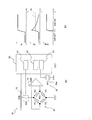
- FIG. 3A is a conceptual diagram showing an example of a circuit formed by using the pressure sensor 10.
- the first to fourth resistors R1 to R4 included in the pressure detection circuit 32 form a bridge circuit.
- the output signal V Todayut of the pressure detection circuit 32 is input to the pressure signal input unit 82 of the microprocessor 80 via the amplifier 73.
- power is supplied to the first to fourth resistors R1 to R4 constituting the pressure detection circuit 32, or the first to fourth resistors are supplied on the membrane 22.
- An electrode portion for transmitting the output signal V Centerut of the pressure detection circuit 32 by the bodies R1 to R4 is formed.
- the pressure detection circuit 32 is electrically connected to the substrate portion 70 via the electrode portion and the connection wiring 92 (see FIG. 1).
- the piezoelectric body 35 having the first piezoelectric body portion 35a is not connected to the pressure detection circuit 32 at least on the membrane 22, and is independent of the pressure detection circuit 32. Distortion can be detected.
- the detection signal Vtr1 of the first piezoelectric body portion 35a is input to the detection signal input unit 83 of the microprocessor 80.
- the pressure sensor 10 has a switching unit 72 that switches the power supply to the pressure detection circuit 32 based on the detection signal Vtr from the piezoelectric body 35.
- the microprocessor 80, the switching unit 72, and the amplifier 73 shown in FIG. 3 can be arranged on the substrate unit 70, for example, but their arrangement locations are not particularly limited.
- the switching unit 72 has a switch arranged on the board unit 70 (see FIG. 1), and when the switch is turned on, power is supplied to the pressure detection circuit 32, and when the switch is turned off, power is supplied to the pressure detection circuit 32. Is stopped. ON / OFF of the switching unit 72 is controlled by the switch control unit 81 of the microprocessor 80.
- the switch control unit 81 controls the switching unit 72 based on the detection signal Vtr of the piezoelectric body 35 based on the detection signal Vtr1 by the first piezoelectric body portion 35a.
- the detection signal Vtr of the piezoelectric body 35 input to the pressure signal input unit 82 is the first piezoelectric body. It is the same as the detection signal Vtr1 by the portion 35a.
- FIG. 3B is a graph showing an example of the output results of the pressure P, the detection signal Vtr, and the output signal V MUSTut in the pressure sensor 10 having the circuit shown in FIG. 3A.
- the vertical axis of the graph shown in FIG. 4 indicates the height of the pressure P, the detection signal Vtr, and the signal strength of the output signal V thoroughlyut, and the horizontal axis of the graph indicates the time t.
- the graph shown in FIG. 3B assumes a case where positive strain occurs in the third strain region 27 in which the first piezoelectric body portion 35a is arranged, but as shown in FIG. 2, the third strain region Even when a negative distortion occurs in 27, it can be considered in the same manner if the distortion is taken as an absolute value, for example.
- the switch control unit 81 shown in FIG. 3A recognizes that the detection signal Vtr is not equal to or higher than the predetermined value VL via the detection signal input unit 83, and turns off the switch of the switching unit 72. Keep in state.
- the predetermined value VL for switching the power supply ON / OFF can be determined based on, for example, the pressure and the pressure fluctuation that trigger the pressure detection by the pressure sensor 10.
- the strain or the change in strain generated in the third strain region 27 becomes large.
- the detection signal Vtr detected by the piezoelectric body 35 becomes a predetermined value VL or more (time T1).
- the switch control unit 81 shown in FIG. 3A recognizes that the detection signal Vtr has reached a predetermined value VL or more via the detection signal input unit 83, and the switch of the switching unit 72 is turned on. Switch to.
- the switch of the switching unit 72 shown in FIG. 3A When the switch of the switching unit 72 shown in FIG. 3A is ON, power is supplied to the pressure detection circuit 32. Therefore, as shown in the right part of the graph at the bottom of FIG. 3B, the pressure detection circuit 32 having the first to fourth resistors R1 to R4 detects the strain of the membrane 22 caused by the pressure, and the pressure detection circuit. The value of the output signal V Thut from 32 changes depending on the pressure P.
- the switch of the switching unit 72 may be kept in the ON state until the predetermined timing even if the detection signal Vtr becomes smaller than the predetermined value VL, and corresponds to the case where the detection signal Vtr becomes smaller than the predetermined value VL. Then, it may be switched from ON to OFF (see FIG. 8B).
- the pressure sensor 10 power is not supplied to the pressure detection circuit 32 forming the bridge circuit until the piezoelectric body 35 detects the deformation of the membrane 22 in which the detection signal Vtr exceeds the predetermined value VL. Therefore, the pressure sensor 10 can realize low power consumption. Further, since the pressure sensor 10 uses the piezoelectric body 35 to constantly detect the pressure to be measured, the power supply by the switching unit 72 is appropriately switched even when a momentary pressure rise occurs. , Pressure change detection omission can be prevented.
- the pressure detection accuracy of the piezoelectric body 35 is sufficient as long as the power supply by the switching unit 72 can be appropriately switched, and may be lower than the pressure detection accuracy of the pressure detection circuit 32 forming the bridge circuit.
- the piezoelectric body 35 detects the deformation of the membrane 22 corresponding to the pressure like the pressure detection circuit 32, but unlike the pressure detection circuit 32 using the resistors R1 to R4, the deformation of the membrane 22 As a result, it is polarized and spontaneously creates a potential difference on the surface. Therefore, the piezoelectric body 35 can act as a sensor for switching the power supply to the pressure detection circuit 32 without supplying electric power from the outside, and also to the piezoelectric body 35 formed on the membrane 22. Wiring is also simple.
- the stem 20 having the membrane 22 as shown in FIG. 2, the pressure detection circuit 32 provided on the membrane 22, and the piezoelectric body 35 are manufactured, for example, as follows. First, the stem 20 having the membrane 22 is manufactured by machining.
- the material of the stem 20 is not particularly limited as long as it causes appropriate elastic deformation, and examples thereof include metals and alloys such as stainless steel.
- a semiconductor thin film or a metal thin film is formed on the membrane 22 with an insulating film sandwiched therein, and a piezoelectric thin film is further partially formed, and a semiconductor such as laser processing or screen printing is formed on these thin films.
- the pressure detection circuit 32 including the first to fourth resistors R1 to R4 and the first piezoelectric body portion 35a as shown in FIG. 2 are formed by performing microfabrication or the like by a processing technique. If necessary, an insulating surface layer may be formed on the pressure detection circuit 32 and the upper surface portion of the first piezoelectric body portion 35a.
- the pressure sensor 10 in which the piezoelectric body 35 has a first piezoelectric body portion 35a made of a thin film piezoelectric body and is manufactured by using semiconductor processing technology is advantageous from the viewpoint of miniaturization.
- FIG . 4 is a schematic plan view showing the arrangement of the resistor 31 and the piezoelectric body 135 in the pressure sensor 110 according to the second embodiment.
- the pressure sensor 110 according to the second embodiment is a pressure sensor according to the first embodiment, except that the arrangement of the first piezoelectric body portion 135a included in the piezoelectric body 135 is different from that of the pressure sensor 10 shown in FIG. It is the same as 10.
- the pressure sensor 110 according to the second embodiment will be described focusing on the differences from the pressure sensor 10 according to the first embodiment, and the description of common points will be omitted.
- the piezoelectric body 135 of the pressure sensor 110 has one first piezoelectric body portion 135a, and the first piezoelectric body portion 135a is arranged in a third strain region 27 that causes distortion in the same direction as the first strain position. ing.
- the location of the piezoelectric body 135 is not particularly limited as long as the strain can be detected on the membrane 22, but the piezoelectric body 135 is located in the third strain region 27 which is formed in a wide region on the membrane 22 and causes strain in the same direction. By arranging the piezoelectric body 135, restrictions on the arrangement and size of the piezoelectric body 135 can be relaxed.
- the pressure sensor 110 having the first piezoelectric body portion 135a arranged in the third strain region 27 adopts, for example, the first piezoelectric body portion 135a having a large size to increase the pressure detection sensitivity by the piezoelectric body 135. Can be done. Further, if the detection sensitivity of the piezoelectric body 135 is high, there is a possibility that a circuit such as an amplifier that amplifies the detection signal can be omitted or reduced, which is advantageous from the viewpoint of reducing power consumption and miniaturization.
- the first piezoelectric body portion 135a by arranging the first piezoelectric body portion 135a on the first circumference 24 which is the first strain position, the first piezoelectric body portion 135a becomes the first resistor R1 and the first resistor R1 and the first.
- the direction and magnitude of the strain to be detected can be made uniform with respect to the three resistors R3.
- the pressure sensor 110 the correspondence between the detection signal of the piezoelectric body 135 and the output signal of the pressure detection circuit 32 by the resistor 31 can be grasped with higher accuracy, so that the switching unit of the pressure sensor 110 can be grasped. 72 (see FIG. 3A) can be operated with high accuracy.
- the pressure sensor 110 has the same effect as the pressure sensor 10 with respect to the common portion with the pressure sensor 10 according to the first embodiment.
- FIG . 5 is a schematic plan view showing the arrangement of the resistor 31 and the piezoelectric body 235 in the pressure sensor 210 according to the third embodiment.
- the pressure sensor 210 according to the third embodiment is different from the pressure sensor 110 shown in FIG. 4 in that the piezoelectric body 235 has a plurality of first piezoelectric body portions 235a (two in FIG. 5). This is the same as the pressure sensor 110 according to the second embodiment.
- the pressure sensor 210 according to the third embodiment will be described focusing on the differences from the pressure sensor 110 according to the second embodiment, and the common points will be omitted.
- the piezoelectric body 235 of the pressure sensor 210 has two first piezoelectric body portions 235a, and the two first piezoelectric body portions 235a are in the third strain region 27 which causes distortion in the same direction as the first strain position. Have been placed.
- the two first piezoelectric body portions 235a are both arranged on the first circumference 24, which is the first strain position, but the arrangement of the first piezoelectric body portion 235a is based on this. It is not limited.
- one or both of the two first piezoelectric body portions 235a may be arranged in a third strain region 27 other than on the first circumference 24.
- FIG. 11A is a conceptual diagram showing processing of a detection signal by the microprocessor 80 of the pressure sensor 210.
- the microprocessor 80 calculates the detection signal Vtr by adding the detection signals Vtr1 from the plurality of first piezoelectric body portions 235a.
- the switching unit 72 of the pressure sensor 210 switches the power supply to the pressure detection circuit 32 based on the detection signal Vtr which is the sum of the detection signals Vtrl from the plurality of first piezoelectric body portions 235a (see FIG. 3). ..
- the signal detected by the piezoelectric body 235 can be strengthened by adding the detection signals Vtrl from the plurality of first piezoelectric body portions 235a, so that the switching unit 72 is made higher. It can be operated with precision. Further, the pressure sensor 210 has the same effect as the pressure sensor 110 with respect to the common portion with the pressure sensor 110 according to the second embodiment.
- FIG. 6 is a schematic plan view showing the arrangement of a resistor 31 and the piezoelectric 335 in the pressure sensor 310 according to a fourth embodiment.
- the pressure sensor 310 according to the fourth embodiment is different from the pressure sensor 110 shown in FIG. 4 in that the piezoelectric body 235 has the second piezoelectric body portion 335b in addition to the first piezoelectric body portion 335a. In other respects, it is the same as the pressure sensor 110 according to the second embodiment.
- the pressure sensor 310 according to the fourth embodiment will be described focusing on the differences from the pressure sensor 110 according to the second embodiment, and the common points will be omitted.
- the piezoelectric body 335 of the pressure sensor 310 has a first piezoelectric body portion 335a and a second piezoelectric body portion 335b.
- the first piezoelectric portion 335a is the same as the first piezoelectric portion 135a shown in FIG. 4, and is arranged in the third strain region 27 on the membrane 22.
- the second piezoelectric body portion 335b has a thin film piezoelectric body or the like like the first piezoelectric body portion 335a, and is arranged in the fourth strain region 28 on the membrane 22.
- the fourth strain region 28 is a region on the membrane 22 that causes strain in the same direction as the second circumference 26, which is the second strain position where the second resistor R2 and the fourth resistor R4 are arranged ( (See FIG. 2).
- FIG. 11B is a conceptual diagram showing the processing of the detection signal by the microprocessor 80 of the pressure sensor 310.
- the microprocessor 80 calculates the detection signal Vtr of the difference between the detection signal Vtr1 from the first piezoelectric body portion 335a and the detection signal Vtr2 from the second piezoelectric body portion 335b.
- the switching unit 72 of the pressure sensor 310 connects to the pressure detection circuit 32 based on the detection signal Vtr of the difference between the detection signal Vtr1 from the first piezoelectric body portion 335a and the detection signal Vtr2 from the second piezoelectric body portion 335b. Switch the power supply (see FIG. 3).
- Such a pressure sensor 310 is a signal detected by the piezoelectric body 335 by obtaining a detection signal Vtr of the difference between the detection signal Vtrl from the first piezoelectric body portion 335a and the detection signal Vtr2 from the second piezoelectric body portion 335b. Therefore, the switching unit 72 can be operated with higher accuracy. Further, the pressure sensor 310 has the same effect as the pressure sensor 110 with respect to the common portion with the pressure sensor 110 according to the second embodiment.
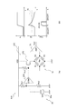
- FIG. 7A is a conceptual diagram showing a circuit of a pressure sensor 410 according to a fifth embodiment.
- the circuit of the pressure sensor 410 shown in FIG. 7A is shown in FIG. 3A in that the detection signal Vtr1 of the first piezoelectric body portion 35a is input to the detection signal input unit 83 after passing through the diode bridge 484.
- the circuit of the pressure sensor 10 shown it is the same as the circuit of the pressure sensor 10 according to the first embodiment in other respects.
- the differences from the pressure sensor 10 according to the first embodiment will be mainly described, and the common points will be omitted.
- the diode bridge 484 shown in FIG. 7A Inverts it and outputs it. Therefore, the detection signal Vtr of the piezoelectric body 35 input to the detection signal input unit 83 shown in FIG. 7A responds to the deformation of the membrane 22 regardless of whether the pressure rises or falls. A positive signal is input.
- FIG. 7B is a graph showing an example of the output results of the pressure P, the detection signal Vtr, and the output signal V MUSTut in the pressure sensor 410 having the circuit shown in FIG. 7A.
- the detection signal Vtr that is detected and input to the detection signal input unit 83 is smaller than the predetermined value VL.
- the switch control unit 81 shown in FIG. 7A keeps the switch of the switching unit 72 in the OFF state.
- the switch control unit 81 shown in FIG. 7A recognizes that the detection signal Vtr has reached a predetermined value VL or more via the detection signal input unit 83, and the switch of the switching unit 72 is turned on. Switch to.
- the diode bridge 484 is arranged between the first piezoelectric body portion 35a and the detection signal input portion 82, so that even when the pressure rises as shown in FIG. Even when the pressure drops as shown in FIG. 7B, the power supply to the pressure detection circuit 32 can be started by using a predetermined pressure fluctuation as a trigger.
- the pressure sensor 310 has the same effect as the pressure sensor 10 with respect to the common portion with the pressure sensor 10 according to the second embodiment.
- FIG. 8 (a) is a conceptual diagram showing a circuit of a pressure sensor 510 according to the sixth embodiment.
- the switching unit 572 is not a switch controlled by the microprocessor 80 as shown in FIG. 3A, but is composed of a transistor 575 or the like.
- other points are the same as the circuit of the pressure sensor 10 according to the first embodiment.
- the differences from the pressure sensor 10 according to the first embodiment will be mainly described, and the common points will be omitted.
- the switching unit 572 of the pressure sensor 510 is realized by a circuit consisting of a resistor R Cincinnati1, two resistors R Cincinnati2, a comparator 576, and a transistor 575.
- a transistor 575 is arranged at the entrance from the power supply voltage VDD to the pressure detection circuit 32, and the power supply to the pressure detection circuit 32 is switched by the transistor 575.
- the detection signal Vtr1 of the first piezoelectric body portion 35a is binarized by the comparator 576 and input to the third terminal of the transistor 575.
- ON / OFF of the power supply to the pressure detection circuit 32 is switched based on the detection signal Vtr1 from the first piezoelectric body portion 35a.
- FIG. 8B is a graph showing an example of the output results of the pressure P, the detection signal Vtr1 and the output signal V Brightonut in the pressure sensor 510 having the circuit shown in FIG. 8A.
- the deformation of the membrane 22 is detected by the first piezoelectric body portion 35a, and the detection thereof is detected.
- the switching unit 572 can switch the power supply to the pressure detection circuit 32.
- the pressure sensor 510 has the same effect as the pressure sensor 10 with respect to the common portion with the pressure sensor 10 according to the first embodiment.
- FIG. 9 (a) is a conceptual diagram showing a circuit of a pressure sensor 610 according to the seventh embodiment.
- the circuit of the pressure sensor 610 shown in FIG. 9A is a pressure sensor shown in FIG. 8A in that the detection signal Vtr1 of the first piezoelectric body portion 35a is input to the comparator 576 after passing through the diode bridge 684.
- the circuit of 510 it is the same as the circuit of the pressure sensor 510 according to the sixth embodiment in other respects.
- the differences from the pressure sensor 510 according to the sixth embodiment will be mainly described, and the common points will be omitted.
- the diode bridge 684 shown in FIG. 9A outputs the detection signal Vtr1 of the first piezoelectric body portion 35a by inverting it when the detection signal Vtr1 is a negative voltage. .. Therefore, a positive signal corresponding to the deformation of the membrane 22 is input to the comparator 576 shown in FIG. 9A regardless of whether the pressure is increasing or decreasing.
- FIG. 9B is a graph showing an example of the output results of the pressure P, the detection signal Vtr1 and the output signal V MUSTut in the pressure sensor 610 having the circuit shown in FIG. 9A.
- the deformation of the membrane 22 is detected by the first piezoelectric body portion 35a, and the detection thereof is detected.
- the switching unit 572 can switch the power supply to the pressure detection circuit 32.
- the pressure sensor 610 has the same effect as the pressure sensor 510 with respect to the common portion with the pressure sensor 510 according to the sixth embodiment.
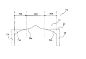
- FIG. 10 is a schematic sectional view of a pressure sensor 710 according to the eighth embodiment.
- the pressure sensor 710 differs from the pressure sensor 10 shown in FIG. 2 in that it has a fillet portion 730, but is the same as the pressure sensor 10 according to the first embodiment in other respects.
- the differences from the pressure sensor 10 according to the first embodiment will be mainly described, and the common points will be omitted.
- the fillet portion 730 connects the side wall 29 to which the outer edge portion 23 of the membrane 22 is connected and the inner surface 22a of the membrane 22.
- the fillet portion 730 is connected not to the entire inner surface 22a of the inner surface 22a of the membrane 22 but only to a predetermined range inside from the outer edge portion 23 of the membrane 22.
- the fillet portion 730 gradually becomes thinner from the side wall 29 toward the center side of the membrane 22, and is not connected to the fourth strain region 728 on the center side of the membrane 22.
- the fillet portion 730 may be made of the same material as the side wall 29 or the inner surface 22a of the membrane 22, or may be made of a different material.
- the pressure sensor 710 having the fillet portion 730 tends to have a larger ratio of the third strain region 727 to the fourth strain region 728 than the pressure sensor 10 having no fillet portion. Therefore, the pressure sensor 710 having the fillet portion 730 shown in FIG. 10 can easily secure a sufficient arrangement space when the first piezoelectric body portion 25a is arranged in the third strain region 727. Therefore, such a pressure sensor 710 can increase the detection output of the piezoelectric body and is advantageous for miniaturization. Further, the pressure sensor 710 has the same effect as the pressure sensor 10 with respect to the common portion with the pressure sensor 10 according to the first embodiment.
- the pressure sensor according to the present invention has been described with reference to the embodiments, but the present invention is not limited to these embodiments, and may include many other embodiments and modifications. Needless to say.
- the number and arrangement of the first piezoelectric portions 35a, 135a, 235a, 335a and the second piezoelectric portion 335b are not limited to those shown in FIGS. 2, 4 to 6, and strain is generated on the membrane 22. It can be placed anywhere it occurs.
- the membrane of the pressure sensor is not limited to the stem and the metal plate, and membranes of other shapes and materials can be used.
Landscapes
- Physics & Mathematics (AREA)
- General Physics & Mathematics (AREA)
- Chemical & Material Sciences (AREA)
- Analytical Chemistry (AREA)
- Measuring Fluid Pressure (AREA)
Abstract
【課題】低消費電力化が可能であって、圧力変化の検出漏れを防止可能な圧力センサを提供する。 【解決手段】圧力に応じた変形を生じるメンブレンと、メンブレン上に配置される少なくとも4つの抵抗体を含み、抵抗体によるブリッジ回路を形成してメンブレンの変形を検出する圧力検出回路と、メンブレン上に配置されておりメンブレンの変形を検出する圧電体と、圧電体からの検出信号に基づいて、圧力検出回路への電力供給を切り換える切換部と、を有する圧力センサ。
Description
本発明は、メンブレンの変形による歪を抵抗変化により検出する圧力センサに関する。
圧抵抗効果(ピエゾ抵抗効果ともいう)を利用して、メンブレン(ダイアフラムともいう)の歪を抵抗変化により検出する圧力センサが知られている。このような圧力センサでは、メンブレンの変形による歪を、メンブレン上に設けられた抵抗体の抵抗変化により検出する。
また、近年、圧力センサの低消費電力化が求められており、たとえば、圧力センサに含まれるブリッジ回路への電力供給を、パルス駆動によって間欠的に行う技術が提案されている(特許文献1参照)。
しかしながら、間欠的に電力供給を行う圧力センサでは、電力供給がOFFのタイミングで発生した瞬間的な圧力異常を検出できないという課題を有している。
本発明は、低消費電力化が可能であって、圧力変化の検出漏れを防止可能な圧力センサを提供する。
上記目的を達成するために、本発明に係る圧力センサは、
圧力に応じた変形を生じるメンブレンと、
前記メンブレン上に配置される少なくとも4つの抵抗体を含み、前記抵抗体によるブリッジ回路を形成して前記メンブレンの変形を検出する圧力検出回路と、
前記メンブレン上に配置されており前記メンブレンの変形を検出する圧電体と、
前記圧電体からの検出信号に基づいて、前記圧力検出回路への電力供給を切り換える切換部と、を有する。
圧力に応じた変形を生じるメンブレンと、
前記メンブレン上に配置される少なくとも4つの抵抗体を含み、前記抵抗体によるブリッジ回路を形成して前記メンブレンの変形を検出する圧力検出回路と、
前記メンブレン上に配置されており前記メンブレンの変形を検出する圧電体と、
前記圧電体からの検出信号に基づいて、前記圧力検出回路への電力供給を切り換える切換部と、を有する。
本発明に係る圧力センサは、抵抗体によってブリッジ回路を形成して圧力を計測する圧力検出回路とは別に、メンブレン上に配置された圧電体と、圧電体からの検出信号に基づいて圧力検出回路への電力供給を切り換える切換部を有する。このような圧力センサは、たとえば、検出信号に応じて電力供給を停止・再開等することにより、必要な圧力範囲においてのみ圧力検出を行うことができるため、低消費電力化が可能である。また、圧電体は、メンブレン上に配置されているため、このような圧電体からの検出信号に基づくことにより、切換部は、電力供給の停止・再開を精度良く行うことができ、圧力変化の検出漏れを防止することができる。また、圧電体は、メンブレンの変形により圧電効果を生じる。したがって、このような圧力センサは、圧電体によるメンブレンの変形の検出および切換部による電力供給のために必要な電力を抑制することが可能であり、この点でも低消費電力化に資する。
また、たとえば、前記圧力検出回路に含まれる前記抵抗体には、前記メンブレン上において所定の歪特性を生じる第1歪位置に配置される第1抵抗体および第3抵抗体と、前記第1歪位置とは異なる方向の歪特性を生じる第2歪位置に配置される第2抵抗体および第4抵抗体とを含み、
前記第1歪位置は、前記メンブレン上において前記第2歪位置より外周側に位置し、
前記圧電体は、前記メンブレン上において前記第1歪位置と同方向の歪を生じる第3歪領域に配置されている第1圧電体部分を有する。
前記第1歪位置は、前記メンブレン上において前記第2歪位置より外周側に位置し、
前記圧電体は、前記メンブレン上において前記第1歪位置と同方向の歪を生じる第3歪領域に配置されている第1圧電体部分を有する。
第3歪領域は、第2抵抗体および第4抵抗体が配置される第2歪位置より外周側に位置しており、メンブレン上の比較的広い範囲に広がっているため、圧電体を第3歪領域に配置することにより、レイアウトの自由度を確保できる。また、第3歪領域が広いため、第1圧電体部分として比較的サイズの大きな圧電体を用いることが可能であり、そのような第1圧電体部分を有する圧電体は、メンブレンの変形によって、より大きな起電力を生じることができる。また、検出信号が大きければ、信号を増幅する回路を小さくしたり、または省略することが可能であり、この点でも装置の小型化に資する。また、検出信号が大きければノイズを抑えることができるため、圧電体による検出および切換部によるセンサの精度を高めることも可能である。
また、たとえば、前記圧電体は、前記第1圧電体部分を複数有してもよく、
前記切換部は、前記複数の前記第1圧電体部分からの検出信号を足し合わせた信号に基づいて、前記圧力検出回路への電力供給を切り換えてもよい。
前記切換部は、前記複数の前記第1圧電体部分からの検出信号を足し合わせた信号に基づいて、前記圧力検出回路への電力供給を切り換えてもよい。
上述したように、第3歪領域は広いため、複数の第1圧電体部分を配置するのに適している。また切換部は、複数の第1圧電体部分において同一方向の歪から生じた検出信号を足し合わせた信号に基づくことにより、信号の検出値を大きくすることができる。したがって、このような圧力センサは、信号を増幅する回路を小さくしたり、または省略することが可能であり、圧力センサの小型化に資する。また、検出信号が大きければノイズを抑えることができるため、圧電体による検出および切換部による切換の精度を高めることも可能である。
また、たとえば、前記圧電体は、前記メンブレン上において前記第2歪位置と同方向の歪を生じる第4歪領域に配置されている第2圧電体部分を有してもよく、
前記切換部は、前記第1圧電体部分からの検出信号と前記第2圧電体部分からの検出信号の差分の信号に基づいて、前記圧力検出回路への電力供給を切り換えてもよい。したがって、このような圧力センサは、信号を増幅する回路を小さくしたり、または省略することが可能であり、圧力センサの小型化に資する。また、検出信号が大きければノイズを抑えることができるため、圧電体による検出および切換部による切換の精度を高めることも可能である。
前記切換部は、前記第1圧電体部分からの検出信号と前記第2圧電体部分からの検出信号の差分の信号に基づいて、前記圧力検出回路への電力供給を切り換えてもよい。したがって、このような圧力センサは、信号を増幅する回路を小さくしたり、または省略することが可能であり、圧力センサの小型化に資する。また、検出信号が大きければノイズを抑えることができるため、圧電体による検出および切換部による切換の精度を高めることも可能である。
第1圧電体部分と第2圧電体部分とでは、検出される歪の方向が異なり、符号が逆である検出信号が出力されるため、第1圧電体部分からの検出信号と第2圧電体部分からの検出信号の差分の信号におり、信号の検出値(絶対値)を大きくすることができる。
また、たとえば、前記圧電体は、薄膜による薄膜圧電体を有してもよい。
圧電体が、薄膜圧電体であることにより、圧力センサの小型化に資する。
また、たとえば、本発明に係る圧力センサは、前記メンブレンの外縁部が接続する側壁と、
前記メンブレンにおける前記外縁部から内側の所定範囲と前記側壁とを接続しており、前記側壁から前記メンブレンの中心側へ向かって徐々に厚みが薄くなるフィレット部と、
を有してもよい。
前記メンブレンにおける前記外縁部から内側の所定範囲と前記側壁とを接続しており、前記側壁から前記メンブレンの中心側へ向かって徐々に厚みが薄くなるフィレット部と、
を有してもよい。
フィレット部が形成されることにより、フィレット部が無い場合に比べて、メンブレン上に形成される第3歪領域が広がるため、このような圧力センサは、第1圧電体部分を大きくしたり、複数の第1圧電体部分を配置することが容易となり、圧電体による検出および切換部による切換の精度を高めることが可能である。
以下、本発明を、図面に示す実施形態に基づき説明する。
第1実施形態
図1は、本発明に係る圧力センサ10の概略断面図である。圧力センサ10は、圧力に応じた変形を生じるメンブレン22を有する。図1に示す実施形態では、ステム20の上底が、メンブレン22になっている。圧力センサ10は、メンブレン22を有するステム20の他に、ステム20へ圧力を伝える流路12bが形成されている接続部材12、接続部材12に対してステム20を固定する抑え部材14、メンブレン22上の電極部などに対して配線される基板部70などを有する。
図1は、本発明に係る圧力センサ10の概略断面図である。圧力センサ10は、圧力に応じた変形を生じるメンブレン22を有する。図1に示す実施形態では、ステム20の上底が、メンブレン22になっている。圧力センサ10は、メンブレン22を有するステム20の他に、ステム20へ圧力を伝える流路12bが形成されている接続部材12、接続部材12に対してステム20を固定する抑え部材14、メンブレン22上の電極部などに対して配線される基板部70などを有する。
図1に示すように、接続部材12の外周には、圧力センサ10を測定対象に対して固定するためのねじ溝12aが形成されている。ねじ溝12aを介して圧力センサ10を固定することにより、接続部材12の内部に形成されている流路12bは、測定対象である圧力室に対して気密に連通する。
図1に示すように、ステム20は、有底(上底)筒状の外形状を有しており、接続部材12における流路12bの一方の端部に設けられる。ステム20は、開口部側にフランジ部21が設けられており、抑え部材14と接続部材12との間にフランジ部21が挟み込まれることにより、接続部材12に対して固定される。ステム20の開口部と接続部材12の流路12bとは、抑え部材14を用いて気密に連結されており、測定対象の圧力が、ステム20のメンブレン22に伝えられる。
ステム20の上底であるメンブレン22は、側壁29(図2参照)など、ステム20における他の部分に比べて肉薄になっており、流路12bから伝えられる圧力に応じた変形を生じる。メンブレン22は、圧力流体に接触する内面22aと、内面22aとは反対側の外面22bとを有しており、メンブレン22の外面22b側には、後述する圧力検出回路32、圧電体35(図2参照)や、図示しない電極部などが設けられる。
図1に示す抑え部材14には、メンブレン22の外面22bに形成された圧力検出回路32および圧電体35に対して電気的に接続される配線や電極部などを有する基板部70が固定されている。基板部70の電極部とメンブレン22上の電極部とは、ワイヤボンディングなどにより形成される接続配線92などを介して、電気的に接続されている。基板部70はリング状の外形状を有しており、ステム20は、基板部70の中央に形成される貫通穴を挿通している。
図2は、第1実施形態に係る圧力センサ10における抵抗体31および圧電体35の配置を示す概念図である。図2の上部は、メンブレン22の外面22b側である上方側からステム20を見た概略平面図であり、図2の下部は、ステム20の模式断面図である。
図2に示すように、圧力センサ10は、第1抵抗体R1、第2抵抗体R2、第3抵抗体R3および第4抵抗体R4によるブリッジ回路を形成してメンブレン22の変形を検出する圧力検出回路32と、圧力検出回路32とは独立してメンブレン22の変形を検出する圧電体35とを有する。圧力検出回路32は、メンブレン22の外面22bに配置される少なくとも4つの抵抗体R1~R4を含む。また、圧電体35も、抵抗体R1~R4と同様に、メンブレン22の外面22bに配置されている。
図2上部の概略平面図に示されるように、圧力検出回路32に含まれる抵抗体R1~R4には、第1円周24上に配置される第1抵抗体R1および第3抵抗体R3と、第2円周26上に配置される第2抵抗体R2および第4抵抗体R4が含まれる。図2下部の模式断面図に示されるように、第1円周24上は、メンブレン22上において所定の歪特性を生じる第1歪位置であり、第2円周26上は、メンブレン22上において第1歪位置である第1円周24上と異なる歪特性を生じる第2歪位置である。
図2に示すように、第1歪位置である第1円周24は、第2歪位置である第2円周26より大きい半径を有する円の円周であり、メンブレン22において、第1円周24は、第2円周26より外周側に位置する。たとえば、メンブレン22が内面22aから所定の正圧を受けた場合に、第1円周24上では負の歪-ε(圧縮歪)を生じるのに対して、第2円周26では正の歪+ε(引張歪)を生じる。このように、第1歪位置である第1円周24上における歪特性と、第2歪位置である第2円周26上における歪特性は、互いに異なる方向(符号が異なり打ち消しあう関係)であることが好ましい。
図2に示す圧力検出回路32は、4つの抵抗体R1~R4を有する。ただし、圧力検出回路32が有する抵抗体R1~R4の数は、4つのみには限定されない。たとえば、圧力検出回路32は、5つ以上の抵抗体を用いて、図3に示すようなブリッジ回路を形成するものであってもよい。
また、図2に示す圧力検出回路32は、第1円周24上に配置される抵抗体R1、R3の数と、第2円周26に配置される抵抗体R2、R4の数とが、いずれも2つである。ただし、第1円周24上に配置される抵抗体R1、R3の数および第2円周26上に配置される抵抗体R2、R4の数は、3つ以上であってもよい。また、第1円周24上に配置される抵抗体R1、R3の数と、第2円周26上に配置される抵抗体R2、R4の数とは、同数であってもよく、異なっていてもよい。
図2の上部の平面図に示すように、圧電体35は、第1圧電体部分35aを有する。第1圧電体部分35aは、メンブレン22上において第1歪位置である第1円周24と同方向の歪を生じる第3歪領域27に配置されている。図2の下部の模式断面図に示すように、メンブレン22が内面22aから所定の正圧を受けた場合に、メンブレン22の第3歪領域27では、第1円周24上と同じ負の歪-ε(圧縮歪)を生じる。
図2に示すように、圧電体35が有する第1圧電体部分35aは、第1円周24より中心側の第3歪領域27に配置されている。ただし、第1圧電体部分35aの配置としてはこれに限定されず、第1圧電体部分35aは、第1円周24より外周側の第3歪領域27に配置されていてもよく、第1円周24上に配置されていてもよい。なお、第1円周24上も、第3歪領域27に含まれる。
図3(a)は、圧力センサ10を用いて形成される回路の一例を示す概念図である。図3(a)に示すように、圧力検出回路32に含まれる第1~第4抵抗体R1~R4は、ブリッジ回路を形成している。圧力検出回路32の出力信号Vоutは、アンプ73を介して、マイクロプロセッサ80の圧力信号入力部82に入力される。図2では図示を省略しているが、メンブレン22上には、圧力検出回路32を構成する第1~第4抵抗体R1~R4に対して電力を供給し、または、第1~第4抵抗体R1~R4による圧力検出回路32の出力信号Vоutを伝えるための電極部が形成されている。圧力検出回路32は、電極部および接続配線92(図1参照)を介して、基板部70に電気的に接続されている。
図3(a)に示すように、第1圧電体部分35aを有する圧電体35は、少なくともメンブレン22上では圧力検出回路32に対して接続しておらず、圧力検出回路32とは独立して歪を検出可能である。第1圧電体部分35aの検出信号Vtr1は、マイクロプロセッサ80の検出信号入力部83に入力される。
図3(a)に示すように、圧力センサ10は、圧電体35からの検出信号Vtrに基づいて、圧力検出回路32への電力供給を切り換える切換部72を有する。なお、図3に示すマイクロプロセッサ80、切換部72、およびアンプ73は、たとえば、基板部70に配置することができるが、これらの配置場所は特に限定されない。
切換部72は、基板部70(図1参照)に配置されるスイッチを有し、スイッチがONになると圧力検出回路32へ電力が供給され、スイッチがOFFになると圧力検出回路32への電力供給が停止される。切換部72のON/OFFは、マイクロプロセッサ80のスイッチ制御部81によって制御される。
スイッチ制御部81は、第1圧電体部分35aによる検出信号Vtr1に基づく圧電体35の検出信号Vtrに基づいて、切換部72を制御する。圧力センサ10では、図1に示すように、圧電体35が1つの第1圧電体部分35aを有するため、圧力信号入力部82に入力される圧電体35の検出信号Vtrは、第1圧電体部分35aによる検出信号Vtr1と同じである。
図3(b)は、図3(a)に示す回路を有する圧力センサ10における、圧力Pと、検出信号Vtrと、出力信号Vоutとの出力結果の一例を表すグラフである。なお、図4に示すグラフの縦軸は、圧力Pの高さおよび検出信号Vtr、出力信号Vоutの信号強度を示し、グラフの横軸は時間tを示す。図3(b)に示すグラフは、第1圧電体部分35aが配置される第3歪領域27に正の歪が生じる場合を想定しているが、図2に示すように、第3歪領域27に負の歪が生じる場合であっても、たとえば歪を絶対値とすれば同様に考えることができる。
図3(b)の左側の領域に示すように、圧力センサ10の測定対象である圧力流体の圧力が低く維持される場合、第3歪領域27に生じる歪または歪の変化が小さいため、圧電体35で検出される検出信号Vtrは、所定値VLより小さい。この場合、図3(a)に示すスイッチ制御部81は、検出信号入力部83を介して、検出信号Vtrが所定値VL以上となっていないことを認識し、切換部72のスイッチをOFFの状態に維持する。
図3(a)に示す切換部72のスイッチがOFFの状態では、圧力検出回路32に電力が供給されない。そのため、図3(b)下部のグラフにおける左側部分に示すように、圧力検出回路32は歪を検出せず、圧力検出回路32からの出力信号Vоutの値は変化しない。なお、電力供給のON/OFFを切り換える所定値VLは、たとえば、圧力センサ10による圧力検出を開始すべきトリガーとなる圧力および圧力変動などに基づき定めることができる。
次に、図3(b)の右側の領域に示すように、圧力センサ10の測定対象である圧力流体の圧力が上昇した場合、第3歪領域27に生じる歪または歪の変化が大きくなり、圧電体35で検出される検出信号Vtrは、所定値VL以上となる(時間T1)。この場合、図3(a)に示すスイッチ制御部81は、検出信号入力部83を介して、検出信号Vtrが所定値VL以上となったことを認識し、切換部72のスイッチをONの状態に切り替える。
図3(a)に示す切換部72のスイッチがONの状態では、圧力検出回路32に電力が供給される。そのため、図3(b)下部のグラフにおける右側部分に示すように、第1~第4抵抗体R1~R4を有する圧力検出回路32が、圧力によって生じるメンブレン22の歪を検出し、圧力検出回路32からの出力信号Vоutの値は、圧力Pによって変化する。なお、切換部72のスイッチは、検出信号Vtrが所定値VLより小さくなっても、所定のタイミングまでONの状態に維持されてもよく、検出信号Vtrが所定値VLより小さくなったことに対応してONからOFFへ切り換わってもよい(図8(b)参照)。
このように、圧力センサ10では、圧電体35が検出信号Vtrが所定値VLを超えるメンブレン22の変形を検出するまでは、ブリッジ回路を形成する圧力検出回路32には電力が供給されない。そのため、圧力センサ10は、低消費電力化を実現できる。また、圧力センサ10は、圧電体35を用いて、常に測定対象の圧力を検出しているため、瞬間的な圧力上昇が生じた場合であっても、切換部72による電力供給を適切に切り換え、圧力変化の検出漏れを防止できる。
圧電体35による圧力の検出精度は、切換部72による電力供給を適切に切り換えられる程度であれば足り、ブリッジ回路を形成する圧力検出回路32による圧力の検出精度より低くてもよい。
また、圧電体35は、圧力検出回路32と同様に、圧力に対応するメンブレン22の変形を検出するものであるが、抵抗体R1~R4を用いる圧力検出回路32とは異なり、メンブレン22の変形に伴い分極し、表面に自発的な電位差を生じる。したがって、圧電体35は、外部から電力を供給しなくても、圧力検出回路32への電力供給を切り替えるためのセンサとして作用することができ、また、メンブレン22上に形成する圧電体35への配線もシンプルである。
また、図3(a)に示す回路では、検出信号Vtrの精度向上などのために、圧電体35に対して所定の電圧を印加することも可能である。このような場合であっても、圧電体35はほとんど電流を流さないため、圧電体35を用いる圧力検出では、抵抗体R1~R4などを用いる検出に比べて、消費電力を大幅に小さくすることができる。
図2に示すようなメンブレン22を有するステム20およびメンブレン22上に設けられる圧力検出回路32および圧電体35は、たとえば、以下のようにして作製される。まず、メンブレン22を有するステム20を機械加工により作製する。ステム20の材質は、適切な弾性変形を生じるものであれば特に限定されず、例えばステンレスなどの金属や合金が挙げられる。
次に、メンブレン22の上に、絶縁膜を挟んで半導体薄膜や金属薄膜を形成し、さらに部分的に圧電体薄膜を形成し、これらの薄膜に対してレーザー加工や、スクリーン印刷のような半導体加工技術による微細加工などを行うことにより、図2に示すような第1~第4抵抗体R1~R4を含む圧力検出回路32や第1圧電体部分35aを形成する。なお、必要に応じて、圧力検出回路32や第1圧電体部分35aの上表面の部分には、絶縁性の表面層が形成されてもよい。圧電体35が薄膜圧電体による第1圧電体部分35aを有し、半導体加工技術を用いて作製される圧力センサ10は、小型化の観点で有利である。
第2実施形態
図4は、第2実施形態に係る圧力センサ110における抵抗体31および圧電体135の配置を示す概略平面図である。第2実施形態に係る圧力センサ110は、圧電体135に含まれる第1圧電体部分135aの配置が、図2に示される圧力センサ10とは異なることを除き、第1実施形態に係る圧力センサ10と同様である。第2実施形態に係る圧力センサ110については、第1実施形態に係る圧力センサ10との相違点を中心に説明をおこない、共通点の説明については省略する。
図4は、第2実施形態に係る圧力センサ110における抵抗体31および圧電体135の配置を示す概略平面図である。第2実施形態に係る圧力センサ110は、圧電体135に含まれる第1圧電体部分135aの配置が、図2に示される圧力センサ10とは異なることを除き、第1実施形態に係る圧力センサ10と同様である。第2実施形態に係る圧力センサ110については、第1実施形態に係る圧力センサ10との相違点を中心に説明をおこない、共通点の説明については省略する。
圧力センサ110の圧電体135は、1つの第1圧電体部分135aを有しており、第1圧電体部分135aは、第1歪位置と同方向の歪を生じる第3歪領域27に配置されている。圧電体135の配置場所は、メンブレン22上で歪が検出できる位置であれば特に限定されないが、メンブレン22上おける広い領域に形成され同じ方向の歪が生じる第3歪領域27に、圧電体135を配置することにより、圧電体135の配置および大きさに関する制約を緩和することができる。したがって、第3歪領域27に配置される第1圧電体部分135aを有する圧力センサ110は、たとえば、サイズの大きい第1圧電体部分135aを採用し、圧電体135による圧力の検出感度を上げることができる。また、圧電体135の検出感度が高ければ、検出信号を増幅させるアンプなどの回路を省略または縮小できる可能性があり、消費電力の低減や小型化の観点でも有利である。
また、図4に示すように、第1圧電体部分135aを、第1歪位置である第1円周24上に配置することにより、第1圧電体部分135aは、第1抵抗体R1および第3抵抗体R3に対して、検出する歪の方向および大きさを揃えることができる。このような圧力センサ110では、圧電体135の検出信号と、抵抗体31による圧力検出回路32による出力信号との対応関係を、より高い精度で把握することができるため、圧力センサ110の切換部72(図3(a)参照)を、高精度に動作させることができる。また、圧力センサ110は、第1実施形態に係る圧力センサ10との共通部分については、圧力センサ10と同様の効果を奏する。
第3実施形態
図5は、第3実施形態に係る圧力センサ210における抵抗体31および圧電体235の配置を示す概略平面図である。第3実施形態に係る圧力センサ210は、圧電体235が、第1圧電体部分235aを複数(図5では2つ)有する点で、図4に示される圧力センサ110とは異なることを除き、第2実施形態に係る圧力センサ110と同様である。第3実施形態に係る圧力センサ210については、第2実施形態に係る圧力センサ110との相違点を中心に説明をおこない、共通点の説明については省略する。
図5は、第3実施形態に係る圧力センサ210における抵抗体31および圧電体235の配置を示す概略平面図である。第3実施形態に係る圧力センサ210は、圧電体235が、第1圧電体部分235aを複数(図5では2つ)有する点で、図4に示される圧力センサ110とは異なることを除き、第2実施形態に係る圧力センサ110と同様である。第3実施形態に係る圧力センサ210については、第2実施形態に係る圧力センサ110との相違点を中心に説明をおこない、共通点の説明については省略する。
圧力センサ210の圧電体235は、2つの第1圧電体部分235aを有しており、2つの第1圧電体部分235aは、第1歪位置と同方向の歪を生じる第3歪領域27に配置されている。なお、圧力センサ210において、2つの第1圧電体部分235aは、いずれも第1歪位置である第1円周24上に配置されているが、第1圧電体部分235aの配置は、これに限定されるものではない。圧電センサ210では、2つの第1圧電体部分235aのうち一方または双方が、第1円周24上以外の第3歪領域27に配置されていてもよい。
圧力センサ210では、図3に示すマイクロプロセッサ80の検出信号入力部83に、2つの第1圧電体部分235aからの検出信号Vtr1が入力される。図11(a)は、圧力センサ210のマイクロプロセッサ80での検出信号の処理を表す概念図である。図11(a)に示すように、マイクロプロセッサ80は、複数の第1圧電体部分235aからの検出信号Vtr1を足し合わせた検出信号Vtrを算出する。そして、圧力センサ210の切換部72は、複数の第1圧電体部分235aからの検出信号Vtrlを足し合わせた検出信号Vtrに基づいて、圧力検出回路32への電力供給を切り換える(図3参照)。
このような圧力センサ210は、複数の第1圧電体部分235aからの検出信号Vtrlを足し合わせることにより、圧電体235によって検出される信号を強くすることができるため、切換部72を、より高精度に動作させることができる。また、圧力センサ210は、第2実施形態に係る圧力センサ110との共通部分については、圧力センサ110と同様の効果を奏する。
第4実施形態
図6は、第4実施形態に係る圧力センサ310における抵抗体31および圧電体335の配置を示す概略平面図である。第4実施形態に係る圧力センサ310は、圧電体235が、第1圧電体部分335aに加えて、第2圧電体部分335bを有する点で、図4に示される圧力センサ110とは異なるが、その他の点では、第2実施形態に係る圧力センサ110と同様である。第4実施形態に係る圧力センサ310については、第2実施形態に係る圧力センサ110との相違点を中心に説明をおこない、共通点の説明については省略する。
図6は、第4実施形態に係る圧力センサ310における抵抗体31および圧電体335の配置を示す概略平面図である。第4実施形態に係る圧力センサ310は、圧電体235が、第1圧電体部分335aに加えて、第2圧電体部分335bを有する点で、図4に示される圧力センサ110とは異なるが、その他の点では、第2実施形態に係る圧力センサ110と同様である。第4実施形態に係る圧力センサ310については、第2実施形態に係る圧力センサ110との相違点を中心に説明をおこない、共通点の説明については省略する。
図6に示すように、圧力センサ310の圧電体335は、第1圧電体部分335aと第2圧電体部分335bを有する。第1圧電体部分335aは、図4に示す第1圧電体部分135aと同様であり、メンブレン22上の第3歪領域27に配置されている。第2圧電体部分335bは、第1圧電体部分335aと同様に薄膜圧電体などを有しており、メンブレン22上の第4歪領域28に配置されている。第4歪領域28は、メンブレン22上において、第2抵抗体R2および第4抵抗体R4が配置されている第2歪位置である第2円周26と同方向の歪を生じる領域である(図2参照)。
圧力センサ310では、図3に示すマイクロプロセッサ80の検出信号入力部83に、第1圧電体部分335aからの検出信号Vtr1と、第2圧電体部分からの検出信号Vtr2とが入力される。図11(b)は、圧力センサ310のマイクロプロセッサ80での検出信号の処理を表す概念図である。図11(b)に示すように、マイクロプロセッサ80は、第1圧電体部分335aからの検出信号Vtr1と第2圧電体部分335bからの検出信号Vtr2の差分の検出信号Vtrを算出する。そして、圧力センサ310の切換部72は、第1圧電体部分335aからの検出信号Vtr1と第2圧電体部分335bからの検出信号Vtr2の差分の検出信号Vtrに基づいて、圧力検出回路32への電力供給を切り換える(図3参照)。
このような圧力センサ310は、第1圧電体部分335aからの検出信号Vtrlと第2圧電体部分335bからの検出信号Vtr2の差分の検出信号Vtrを得ることにより、圧電体335によって検出される信号を強くすることができるため、切換部72を、より高精度に動作させることができる。また、圧力センサ310は、第2実施形態に係る圧力センサ110との共通部分については、圧力センサ110と同様の効果を奏する。
第5実施形態
図7(a)は、第5実施形態に係る圧力センサ410の回路を示す概念図である。図7(a)に示す圧力センサ410の回路は、第1圧電体部分35aの検出信号Vtr1が、ダイオードブリッジ484を通った後に検出信号入力部83に入力する点で、図3(a)に示す圧力センサ10の回路とは異なるが、その他の点では、第1実施形態に係る圧力センサ10の回路と同様である。第5実施形態に係る圧力センサ410の説明では、第1実施形態に係る圧力センサ10との相違点を中心に説明を行い、共通点については説明を省略する。
図7(a)は、第5実施形態に係る圧力センサ410の回路を示す概念図である。図7(a)に示す圧力センサ410の回路は、第1圧電体部分35aの検出信号Vtr1が、ダイオードブリッジ484を通った後に検出信号入力部83に入力する点で、図3(a)に示す圧力センサ10の回路とは異なるが、その他の点では、第1実施形態に係る圧力センサ10の回路と同様である。第5実施形態に係る圧力センサ410の説明では、第1実施形態に係る圧力センサ10との相違点を中心に説明を行い、共通点については説明を省略する。
図7(a)に示すダイオードブリッジ484は、第1圧電体部分35aの検出信号Vtr1が負電圧である場合、これを反転させて出力する。したがって、図7(a)に示す検出信号入力部83に入力される圧電体35の検出信号Vtrは、圧力上昇時であっても、圧力低下時であっても、メンブレン22の変形に応じた正の信号が入力される。
図7(b)は、図7(a)に示す回路を有する圧力センサ410における、圧力Pと、検出信号Vtrと、出力信号Vоutとの出力結果の一例を表すグラフである。図7(b)の左側の領域に示すように、圧力センサ410の測定対象である圧力流体の圧力が高く維持される場合、メンブレン22に生じる歪または歪の変化が小さいため、圧電体35で検出され、検出信号入力部83に入力される検出信号Vtrは、所定値VLより小さい。この場合、図7(a)に示すスイッチ制御部81は、切換部72のスイッチをOFFの状態に維持する。
図7(b)に示す切換部72のスイッチがOFFの状態では、圧力検出回路32に電力が供給されない。そのため、図7(b)下部のグラフにおける左側部分に示すように、圧力検出回路32は歪を検出せず、圧力検出回路32からの出力信号Vоutの値は変化しない。
次に、図7(b)の右側の領域に示すように、圧力センサ410の測定対象である圧力流体の圧力が低下した場合、圧電体35で検出され、検出信号入力部83に入力される検出信号Vtrは、所定値VL以上となる(時間T1)。この場合、図7(a)に示すスイッチ制御部81は、検出信号入力部83を介して、検出信号Vtrが所定値VL以上となったことを認識し、切換部72のスイッチをONの状態に切り替える。
図7(a)に示す切換部72のスイッチがONの状態では、圧力検出回路32に電力が供給される。そのため、図7(b)下部のグラフにおける右側部分に示すように、第1~第4抵抗体R1~R4を有する圧力検出回路32が、圧力によって生じるメンブレン22の歪を検出し、圧力検出回路32からの出力信号Vоutの値は、圧力Pによって変化する。
このように、圧力センサ410では、第1圧電体部分35aと検出信号入力部82との間にダイオードブリッジ484が配置されていることにより、図3(b)に示すような圧力上昇時でも、図7(b)に示すような圧力低下時でも、所定の圧力変動をトリガーとして、圧力検出回路32への電力供給を開始することができる。また、圧力センサ310は、第2実施形態に係る圧力センサ10との共通部分については、圧力センサ10と同様の効果を奏する。
第6実施形態
図8(a)は、第6実施形態に係る圧力センサ510の回路を示す概念図である。図8(a)に示す圧力センサ510の回路は、切換部572が、図3(a)に示すようなマイクロプロセッサ80に制御されるスイッチではなく、トランジスタ575などにより構成されている点で、図3(a)に示す圧力センサ10とは異なるが、その他の点は、第1実施形態に係る圧力センサ10の回路と同様である。第6実施形態に係る圧力センサ510の説明では、第1実施形態に係る圧力センサ10との相違点を中心に説明を行い、共通点については説明を省略する。
図8(a)は、第6実施形態に係る圧力センサ510の回路を示す概念図である。図8(a)に示す圧力センサ510の回路は、切換部572が、図3(a)に示すようなマイクロプロセッサ80に制御されるスイッチではなく、トランジスタ575などにより構成されている点で、図3(a)に示す圧力センサ10とは異なるが、その他の点は、第1実施形態に係る圧力センサ10の回路と同様である。第6実施形態に係る圧力センサ510の説明では、第1実施形態に係る圧力センサ10との相違点を中心に説明を行い、共通点については説明を省略する。
図8(a)に示すように、圧力センサ510の切換部572は、抵抗Rо1と、2つの抵抗Rо2と、コンパレータ576と、トランジスタ575による回路により実現されている。図5に示す切換部572では、電源電圧VDDから圧力検出回路32への入り口にトランジスタ575が配置されており、トランジスタ575によって、圧力検出回路32への電力の供給が切り換えられる。トランジスタ575の3番目の端子には、第1圧電体部分35aの検出信号Vtr1が、コンパレータ576によって2値化されて入力される。これにより、圧力検出回路32への電力供給のON/OFFが、第1圧電体部分35aからの検出信号Vtr1に基づいて切り換えられる。
図8(b)は、図8(a)に示す回路を有する圧力センサ510における、圧力Pと、検出信号Vtr1と、出力信号Vоutとの出力結果の一例を表すグラフである。図8(b)に示すように、圧力センサ510の回路でも、図3(a)に示す圧力センサ10の回路と同様に、第1圧電体部分35aによりメンブレン22の変形を検出し、その検出信号Vtr1に基づいて、切換部572が圧力検出回路32への電力供給を切り換えることができる。また、圧力センサ510は、第1実施形態に係る圧力センサ10との共通部分については、圧力センサ10と同様の効果を奏する。
第7実施形態
図9(a)は、第7実施形態に係る圧力センサ610の回路を示す概念図である。図9(a)に示す圧力センサ610の回路は、第1圧電体部分35aの検出信号Vtr1が、ダイオードブリッジ684を通った後にコンパレータ576に入力する点で、図8(a)に示す圧力センサ510の回路とは異なるが、その他の点では、第6実施形態に係る圧力センサ510の回路と同様である。第7実施形態に係る圧力センサ610の説明では、第6実施形態に係る圧力センサ510との相違点を中心に説明を行い、共通点については説明を省略する。
図9(a)は、第7実施形態に係る圧力センサ610の回路を示す概念図である。図9(a)に示す圧力センサ610の回路は、第1圧電体部分35aの検出信号Vtr1が、ダイオードブリッジ684を通った後にコンパレータ576に入力する点で、図8(a)に示す圧力センサ510の回路とは異なるが、その他の点では、第6実施形態に係る圧力センサ510の回路と同様である。第7実施形態に係る圧力センサ610の説明では、第6実施形態に係る圧力センサ510との相違点を中心に説明を行い、共通点については説明を省略する。
図9(a)に示すダイオードブリッジ684は、図7(a)に示すダイオードブリッジ484と同様に、第1圧電体部分35aの検出信号Vtr1が負電圧である場合、これを反転させて出力する。したがって、図9(a)に示すコンパレータ576には、圧力上昇時であっても、圧力低下時であっても、メンブレン22の変形に応じた正の信号が入力される。
図9(b)は、図9(a)に示す回路を有する圧力センサ610における、圧力Pと、検出信号Vtr1と、出力信号Vоutとの出力結果の一例を表すグラフである。図9(b)に示すように、圧力センサ610の回路でも、図7(a)に示す圧力センサ410の回路と同様に、第1圧電体部分35aによりメンブレン22の変形を検出し、その検出信号Vtr1に基づいて、切換部572が圧力検出回路32への電力供給を切り換えることができる。また、圧力センサ610は、第6実施形態に係る圧力センサ510との共通部分については、圧力センサ510と同様の効果を奏する。
第8実施形態
図10は、第8実施形態に係る圧力センサ710の模式断面図である。圧力センサ710は、フィレット部730を有する点で、図2に示す圧力センサ10とは異なるが、その他の点では、第1実施形態に係る圧力センサ10と同様である。第8実施形態に係る圧力センサ710の説明では、第1実施形態に係る圧力センサ10との相違点を中心に説明を行い、共通点については説明を省略する。
図10は、第8実施形態に係る圧力センサ710の模式断面図である。圧力センサ710は、フィレット部730を有する点で、図2に示す圧力センサ10とは異なるが、その他の点では、第1実施形態に係る圧力センサ10と同様である。第8実施形態に係る圧力センサ710の説明では、第1実施形態に係る圧力センサ10との相違点を中心に説明を行い、共通点については説明を省略する。
図10に示すように、フィレット部730は、メンブレン22の外縁部23が接続する側壁29と、メンブレン22の内面22aを接続している。特に、フィレット部730は、メンブレン22の内面22aの内面22a全体ではなく、メンブレン22おける外縁部23から内側の所定範囲のみに接続している。
フィレット部730は、側壁29からメンブレン22の中心側へ向かって徐々に厚みが薄くなっており、メンブレン22の中心側にある第4歪領域728には接続していない。フィレット部730は、側壁29またはメンブレン22の内面22aと同材質であってもよく、これらとは異なる材質であってもよい。
フィレット部730を有する圧力センサ710は、第4歪領域728に対する第3歪領域727の比率が、フィレット部を有しない圧力センサ10に比べて大きくなる傾向がある。したがって、図10に示すフィレット部730を有する圧力センサ710は、第3歪領域727に第1圧電体部分25aを配置する場合に、十分な配置スペースを容易に確保できる。したがって、このような圧力センサ710は、圧電体の検出出力を強くすることができるとともに、小型化に対して有利である。また、圧力センサ710は、第1実施形態に係る圧力センサ10との共通部分については、圧力センサ10と同様の効果を奏する。
以上のように、実施形態を挙げて本発明に係る圧力センサを説明したが、本発明はこれらの実施形態のみに限定されるものではなく、他の多くの実施形態や変形例を含むことは言うまでもない。たとえば、第1圧電体部分35a、135a、235a、335aおよび第2圧電体部分335bの数および配置は、図2、図4~図6に示すものには限定されず、メンブレン22上において歪が生じる任意の場所に配置することができる。また、圧力センサのメンブレンは、ステムや金属板のみには限定されず、その他形状および材質のメンブレンを用いることも可能である。
10、110、210、310、410、510、610、710…圧力センサ
12…接続部材
12a…ねじ溝
12b…流路
14…抑え部材
20…ステム
21…フランジ部
22a…内面
22b…外面
22…メンブレン
23…外縁部
24…第1円周(第1歪位置)
26…第2円周(第2歪位置)
27、727…第3歪領域
28、728…第4歪領域
29…側壁
31…抵抗体
32…圧力検出回路
R1…第1抵抗体
R2…第2抵抗体
R3…第3抵抗体
R4…第4抵抗体
35、135、235、335…圧電体
35a、135a、235a、335a…第1圧電体部分
335b…第2圧電体部分
VL…所定値(検出閾値)
70…基板部
72、572…切換部
73…アンプ
80…マイクロプロセッサ
81…スイッチ制御部
82…圧力信号入力部
83…検出信号入力部
92…接続配線
Vоut…出力信号
Vtr、Vtr1…検出信号
P…圧力
484、684…ダイオードブリッジ
575…トランジスタ
576…コンパレータ
Rо1…抵抗
Rо2…抵抗
730…フィレット部
12…接続部材
12a…ねじ溝
12b…流路
14…抑え部材
20…ステム
21…フランジ部
22a…内面
22b…外面
22…メンブレン
23…外縁部
24…第1円周(第1歪位置)
26…第2円周(第2歪位置)
27、727…第3歪領域
28、728…第4歪領域
29…側壁
31…抵抗体
32…圧力検出回路
R1…第1抵抗体
R2…第2抵抗体
R3…第3抵抗体
R4…第4抵抗体
35、135、235、335…圧電体
35a、135a、235a、335a…第1圧電体部分
335b…第2圧電体部分
VL…所定値(検出閾値)
70…基板部
72、572…切換部
73…アンプ
80…マイクロプロセッサ
81…スイッチ制御部
82…圧力信号入力部
83…検出信号入力部
92…接続配線
Vоut…出力信号
Vtr、Vtr1…検出信号
P…圧力
484、684…ダイオードブリッジ
575…トランジスタ
576…コンパレータ
Rо1…抵抗
Rо2…抵抗
730…フィレット部
Claims (6)
- 圧力に応じた変形を生じるメンブレンと、
前記メンブレン上に配置される少なくとも4つの抵抗体を含み、前記抵抗体によるブリッジ回路を形成して前記メンブレンの変形を検出する圧力検出回路と、
前記メンブレン上に配置されており前記メンブレンの変形を検出する圧電体と、
前記圧電体からの検出信号に基づいて、前記圧力検出回路への電力供給を切り換える切換部と、を有する圧力センサ。 - 前記圧力検出回路に含まれる前記抵抗体には、前記メンブレン上において所定の歪特性を生じる第1歪位置に配置される第1抵抗体および第3抵抗体と、前記第1歪位置とは異なる方向の歪特性を生じる第2歪位置に配置される第2抵抗体および第4抵抗体とを含み、
前記第1歪位置は、前記メンブレン上において前記第2歪位置より外周側に位置し、
前記圧電体は、前記メンブレン上において前記第1歪位置と同方向の歪を生じる第3歪領域に配置されている第1圧電体部分を有する請求項1に記載の圧力センサ。 - 前記圧電体は、前記第1圧電体部分を複数有し、
前記切換部は、前記複数の前記第1圧電体部分からの検出信号を足し合わせた信号に基づいて、前記圧力検出回路への電力供給を切り換える請求項2に記載の圧力センサ。 - 前記圧電体は、前記メンブレン上において前記第2歪位置と同方向の歪を生じる第4歪領域に配置されている第2圧電体部分を有し、
前記切換部は、前記第1圧電体部分からの検出信号と前記第2圧電体部分からの検出信号の差分の信号に基づいて、前記圧力検出回路への電力供給を切り換える請求項2に記載の圧力センサ。 - 前記圧電体は、薄膜による薄膜圧電体を有する請求項1から請求項4までのいずれかに記載の圧力センサ。
- 前記メンブレンの外縁部が接続する側壁と、
前記メンブレンにおける前記外縁部から内側の所定範囲と前記側壁とを接続しており、前記側壁から前記メンブレンの中心側へ向かって徐々に厚みが薄くなるフィレット部と、を有する請求項2から4までのいずれかに記載の圧力センサ。
Priority Applications (1)
| Application Number | Priority Date | Filing Date | Title |
|---|---|---|---|
| EP21761057.5A EP4113087B1 (en) | 2020-02-25 | 2021-02-16 | Pressure sensor |
Applications Claiming Priority (2)
| Application Number | Priority Date | Filing Date | Title |
|---|---|---|---|
| JP2020-029308 | 2020-02-25 | ||
| JP2020029308A JP7359032B2 (ja) | 2020-02-25 | 2020-02-25 | 圧力センサ |
Publications (1)
| Publication Number | Publication Date |
|---|---|
| WO2021172103A1 true WO2021172103A1 (ja) | 2021-09-02 |
Family
ID=77491554
Family Applications (1)
| Application Number | Title | Priority Date | Filing Date |
|---|---|---|---|
| PCT/JP2021/005734 Ceased WO2021172103A1 (ja) | 2020-02-25 | 2021-02-16 | 圧力センサ |
Country Status (3)
| Country | Link |
|---|---|
| EP (1) | EP4113087B1 (ja) |
| JP (1) | JP7359032B2 (ja) |
| WO (1) | WO2021172103A1 (ja) |
Families Citing this family (1)
| Publication number | Priority date | Publication date | Assignee | Title |
|---|---|---|---|---|
| FR3161028B1 (fr) * | 2024-04-08 | 2026-04-17 | Wormsensing | Capteur de deformation hybride combinant une jauge piezoelectrique et une jauge resistive |
Citations (5)
| Publication number | Priority date | Publication date | Assignee | Title |
|---|---|---|---|---|
| JPH06194243A (ja) | 1992-10-01 | 1994-07-15 | Motorola Inc | パルス駆動圧力センサ回路とその使用方法 |
| WO2011010571A1 (ja) * | 2009-07-24 | 2011-01-27 | ローム株式会社 | 半導体圧力センサ、圧力センサ装置、電子機器、および半導体圧力センサの製造方法 |
| JP2015068704A (ja) * | 2013-09-27 | 2015-04-13 | セイコーインスツル株式会社 | 圧力センサ |
| JP2015130520A (ja) * | 2009-03-23 | 2015-07-16 | ソナベーション, インコーポレイテッド | 改良圧電識別デバイスおよびその用途 |
| US20160233797A1 (en) * | 2013-09-16 | 2016-08-11 | Board Of Trustees Of Michigan State University | Self-Powered Sensing System For The Monitoring Of Quasi-Static Structural Response |
Family Cites Families (8)
| Publication number | Priority date | Publication date | Assignee | Title |
|---|---|---|---|---|
| FR2496380A1 (fr) * | 1980-12-15 | 1982-06-18 | Thomson Csf | Dispositif piezoresistif a commande electrique |
| JPH08105806A (ja) * | 1994-10-03 | 1996-04-23 | Philips Japan Ltd | 圧電センサシステム |
| EP1177816B1 (en) * | 2000-08-01 | 2004-11-03 | Head Technology GmbH | Racket for ball sports and method for manufacturing thereof |
| JP2008267862A (ja) * | 2007-04-17 | 2008-11-06 | Hitachi Ltd | タイヤ内の気体圧力測定装置 |
| JP5161305B2 (ja) * | 2008-06-05 | 2013-03-13 | 北陸電気工業株式会社 | タッチパネルを備えた表示装置及び圧電アクチュエータ |
| JP5900536B2 (ja) * | 2013-09-30 | 2016-04-06 | 株式会社デンソー | センサ信号検出装置 |
| JP6511929B2 (ja) * | 2015-04-15 | 2019-05-15 | 株式会社明電舎 | 遠方監視システム及び端末装置 |
| US11552240B2 (en) * | 2017-10-24 | 2023-01-10 | Purdue Research Foundation | Machines and processes for producing polymer films and films produced thereby |
-
2020
- 2020-02-25 JP JP2020029308A patent/JP7359032B2/ja active Active
-
2021
- 2021-02-16 EP EP21761057.5A patent/EP4113087B1/en active Active
- 2021-02-16 WO PCT/JP2021/005734 patent/WO2021172103A1/ja not_active Ceased
Patent Citations (5)
| Publication number | Priority date | Publication date | Assignee | Title |
|---|---|---|---|---|
| JPH06194243A (ja) | 1992-10-01 | 1994-07-15 | Motorola Inc | パルス駆動圧力センサ回路とその使用方法 |
| JP2015130520A (ja) * | 2009-03-23 | 2015-07-16 | ソナベーション, インコーポレイテッド | 改良圧電識別デバイスおよびその用途 |
| WO2011010571A1 (ja) * | 2009-07-24 | 2011-01-27 | ローム株式会社 | 半導体圧力センサ、圧力センサ装置、電子機器、および半導体圧力センサの製造方法 |
| US20160233797A1 (en) * | 2013-09-16 | 2016-08-11 | Board Of Trustees Of Michigan State University | Self-Powered Sensing System For The Monitoring Of Quasi-Static Structural Response |
| JP2015068704A (ja) * | 2013-09-27 | 2015-04-13 | セイコーインスツル株式会社 | 圧力センサ |
Non-Patent Citations (1)
| Title |
|---|
| See also references of EP4113087A4 |
Also Published As
| Publication number | Publication date |
|---|---|
| JP7359032B2 (ja) | 2023-10-11 |
| JP2021135084A (ja) | 2021-09-13 |
| EP4113087B1 (en) | 2024-10-16 |
| EP4113087A1 (en) | 2023-01-04 |
| EP4113087A4 (en) | 2024-03-27 |
Similar Documents
| Publication | Publication Date | Title |
|---|---|---|
| Shirinov et al. | Pressure sensor from a PVDF film | |
| KR101440196B1 (ko) | 마이크로폰 및 마이크로폰을 캘리브레이션하기 위한 방법 | |
| US11137302B2 (en) | Compound sensor | |
| JPWO2017068711A1 (ja) | Mems装置 | |
| WO2021172103A1 (ja) | 圧力センサ | |
| US7219551B2 (en) | Differential pressure sensor | |
| TW202237524A (zh) | 壓力感測器及操作壓力感測器的方法 | |
| EP3933366A1 (en) | Pressure sensor | |
| US10908035B2 (en) | Pressure sensor | |
| US20240344910A1 (en) | Capacitive pressure sensor for detecting a pressure, comprising two pressure ranges, and production methods | |
| US20240288324A1 (en) | Pressure sensor with contact detection of the deflection of the membrane, pressure sensor system and method for generating a pressure signal | |
| JP7294009B2 (ja) | 圧力センサ | |
| JP7443833B2 (ja) | 圧力センサ | |
| WO2020166661A1 (ja) | 圧力センサ | |
| WO2023037779A1 (ja) | 圧力センサ | |
| EP4306924A1 (en) | Pressure sensor and sensor system | |
| WO2015133128A1 (ja) | 物理量検出装置 | |
| EP4209764A1 (en) | Pressure sensor | |
| US12607524B2 (en) | Notification sensor arrangement for a differential pressure sensor and a method for outputting a sensed warning signal | |
| CN107607250B (zh) | 一种气压量测装置及气压量测方法 | |
| WO2012063477A1 (ja) | 圧力センサ | |
| CN118696219A (zh) | 微机械压力传感器以及制造方法和用于检测压力参量的方法 | |
| CN120659976A (zh) | 用于补偿对电容式压力测量单元的温度冲击的方法 | |
| KR20030038275A (ko) | 전기 용량식 압력센서 | |
| JPH06186105A (ja) | 圧力センサ |
Legal Events
| Date | Code | Title | Description |
|---|---|---|---|
| 121 | Ep: the epo has been informed by wipo that ep was designated in this application |
Ref document number: 21761057 Country of ref document: EP Kind code of ref document: A1 |
|
| NENP | Non-entry into the national phase |
Ref country code: DE |
|
| ENP | Entry into the national phase |
Ref document number: 2021761057 Country of ref document: EP Effective date: 20220926 |