WO2021176919A1 - 蓄電装置 - Google Patents
蓄電装置 Download PDFInfo
- Publication number
- WO2021176919A1 WO2021176919A1 PCT/JP2021/003599 JP2021003599W WO2021176919A1 WO 2021176919 A1 WO2021176919 A1 WO 2021176919A1 JP 2021003599 W JP2021003599 W JP 2021003599W WO 2021176919 A1 WO2021176919 A1 WO 2021176919A1
- Authority
- WO
- WIPO (PCT)
- Prior art keywords
- power storage
- sensor
- storage element
- bus bar
- detection surface
- Prior art date
- Legal status (The legal status is an assumption and is not a legal conclusion. Google has not performed a legal analysis and makes no representation as to the accuracy of the status listed.)
- Ceased
Links
Images




Classifications
-
- H—ELECTRICITY
- H01—ELECTRIC ELEMENTS
- H01G—CAPACITORS; CAPACITORS, RECTIFIERS, DETECTORS, SWITCHING DEVICES, LIGHT-SENSITIVE OR TEMPERATURE-SENSITIVE DEVICES OF THE ELECTROLYTIC TYPE
- H01G11/00—Hybrid capacitors, i.e. capacitors having different positive and negative electrodes; Electric double-layer [EDL] capacitors; Processes for the manufacture thereof or of parts thereof
- H01G11/10—Multiple hybrid or EDL capacitors, e.g. arrays or modules
-
- H—ELECTRICITY
- H01—ELECTRIC ELEMENTS
- H01G—CAPACITORS; CAPACITORS, RECTIFIERS, DETECTORS, SWITCHING DEVICES, LIGHT-SENSITIVE OR TEMPERATURE-SENSITIVE DEVICES OF THE ELECTROLYTIC TYPE
- H01G9/00—Electrolytic capacitors, rectifiers, detectors, switching devices, light-sensitive or temperature-sensitive devices; Processes of their manufacture
- H01G9/0003—Protection against electric or thermal overload; cooling arrangements; means for avoiding the formation of cathode films
-
- H—ELECTRICITY
- H01—ELECTRIC ELEMENTS
- H01G—CAPACITORS; CAPACITORS, RECTIFIERS, DETECTORS, SWITCHING DEVICES, LIGHT-SENSITIVE OR TEMPERATURE-SENSITIVE DEVICES OF THE ELECTROLYTIC TYPE
- H01G11/00—Hybrid capacitors, i.e. capacitors having different positive and negative electrodes; Electric double-layer [EDL] capacitors; Processes for the manufacture thereof or of parts thereof
- H01G11/14—Arrangements or processes for adjusting or protecting hybrid or EDL capacitors
- H01G11/18—Arrangements or processes for adjusting or protecting hybrid or EDL capacitors against thermal overloads, e.g. heating, cooling or ventilating
-
- H—ELECTRICITY
- H01—ELECTRIC ELEMENTS
- H01G—CAPACITORS; CAPACITORS, RECTIFIERS, DETECTORS, SWITCHING DEVICES, LIGHT-SENSITIVE OR TEMPERATURE-SENSITIVE DEVICES OF THE ELECTROLYTIC TYPE
- H01G11/00—Hybrid capacitors, i.e. capacitors having different positive and negative electrodes; Electric double-layer [EDL] capacitors; Processes for the manufacture thereof or of parts thereof
- H01G11/78—Cases; Housings; Encapsulations; Mountings
- H01G11/82—Fixing or assembling a capacitive element in a housing, e.g. mounting electrodes, current collectors or terminals in containers or encapsulations
-
- H—ELECTRICITY
- H01—ELECTRIC ELEMENTS
- H01G—CAPACITORS; CAPACITORS, RECTIFIERS, DETECTORS, SWITCHING DEVICES, LIGHT-SENSITIVE OR TEMPERATURE-SENSITIVE DEVICES OF THE ELECTROLYTIC TYPE
- H01G2/00—Details of capacitors not covered by a single one of groups H01G4/00-H01G11/00
- H01G2/02—Mountings
-
- H—ELECTRICITY
- H01—ELECTRIC ELEMENTS
- H01G—CAPACITORS; CAPACITORS, RECTIFIERS, DETECTORS, SWITCHING DEVICES, LIGHT-SENSITIVE OR TEMPERATURE-SENSITIVE DEVICES OF THE ELECTROLYTIC TYPE
- H01G9/00—Electrolytic capacitors, rectifiers, detectors, switching devices, light-sensitive or temperature-sensitive devices; Processes of their manufacture
- H01G9/004—Details
- H01G9/08—Housing; Encapsulation
-
- H—ELECTRICITY
- H01—ELECTRIC ELEMENTS
- H01M—PROCESSES OR MEANS, e.g. BATTERIES, FOR THE DIRECT CONVERSION OF CHEMICAL ENERGY INTO ELECTRICAL ENERGY
- H01M10/00—Secondary cells; Manufacture thereof
- H01M10/42—Methods or arrangements for servicing or maintenance of secondary cells or secondary half-cells
- H01M10/48—Accumulators combined with arrangements for measuring, testing or indicating the condition of cells, e.g. the level or density of the electrolyte
- H01M10/486—Accumulators combined with arrangements for measuring, testing or indicating the condition of cells, e.g. the level or density of the electrolyte for measuring temperature
-
- H—ELECTRICITY
- H01—ELECTRIC ELEMENTS
- H01M—PROCESSES OR MEANS, e.g. BATTERIES, FOR THE DIRECT CONVERSION OF CHEMICAL ENERGY INTO ELECTRICAL ENERGY
- H01M50/00—Constructional details or processes of manufacture of the non-active parts of electrochemical cells other than fuel cells, e.g. hybrid cells
- H01M50/20—Mountings; Secondary casings or frames; Racks, modules or packs; Suspension devices; Shock absorbers; Transport or carrying devices; Holders
- H01M50/204—Racks, modules or packs for multiple batteries or multiple cells
- H01M50/207—Racks, modules or packs for multiple batteries or multiple cells characterised by their shape
- H01M50/209—Racks, modules or packs for multiple batteries or multiple cells characterised by their shape adapted for prismatic or rectangular cells
-
- H—ELECTRICITY
- H01—ELECTRIC ELEMENTS
- H01M—PROCESSES OR MEANS, e.g. BATTERIES, FOR THE DIRECT CONVERSION OF CHEMICAL ENERGY INTO ELECTRICAL ENERGY
- H01M50/00—Constructional details or processes of manufacture of the non-active parts of electrochemical cells other than fuel cells, e.g. hybrid cells
- H01M50/20—Mountings; Secondary casings or frames; Racks, modules or packs; Suspension devices; Shock absorbers; Transport or carrying devices; Holders
- H01M50/249—Mountings; Secondary casings or frames; Racks, modules or packs; Suspension devices; Shock absorbers; Transport or carrying devices; Holders specially adapted for aircraft or vehicles, e.g. cars or trains
-
- H—ELECTRICITY
- H01—ELECTRIC ELEMENTS
- H01M—PROCESSES OR MEANS, e.g. BATTERIES, FOR THE DIRECT CONVERSION OF CHEMICAL ENERGY INTO ELECTRICAL ENERGY
- H01M50/00—Constructional details or processes of manufacture of the non-active parts of electrochemical cells other than fuel cells, e.g. hybrid cells
- H01M50/50—Current conducting connections for cells or batteries
- H01M50/502—Interconnectors for connecting terminals of adjacent batteries; Interconnectors for connecting cells outside a battery casing
- H01M50/507—Interconnectors for connecting terminals of adjacent batteries; Interconnectors for connecting cells outside a battery casing comprising an arrangement of two or more busbars within a container structure, e.g. busbar modules
-
- H—ELECTRICITY
- H01—ELECTRIC ELEMENTS
- H01M—PROCESSES OR MEANS, e.g. BATTERIES, FOR THE DIRECT CONVERSION OF CHEMICAL ENERGY INTO ELECTRICAL ENERGY
- H01M50/00—Constructional details or processes of manufacture of the non-active parts of electrochemical cells other than fuel cells, e.g. hybrid cells
- H01M50/50—Current conducting connections for cells or batteries
- H01M50/569—Constructional details of current conducting connections for detecting conditions inside cells or batteries, e.g. details of voltage sensing terminals
-
- H—ELECTRICITY
- H01—ELECTRIC ELEMENTS
- H01M—PROCESSES OR MEANS, e.g. BATTERIES, FOR THE DIRECT CONVERSION OF CHEMICAL ENERGY INTO ELECTRICAL ENERGY
- H01M2220/00—Batteries for particular applications
- H01M2220/20—Batteries in motive systems, e.g. vehicle, ship, plane
-
- Y—GENERAL TAGGING OF NEW TECHNOLOGICAL DEVELOPMENTS; GENERAL TAGGING OF CROSS-SECTIONAL TECHNOLOGIES SPANNING OVER SEVERAL SECTIONS OF THE IPC; TECHNICAL SUBJECTS COVERED BY FORMER USPC CROSS-REFERENCE ART COLLECTIONS [XRACs] AND DIGESTS
- Y02—TECHNOLOGIES OR APPLICATIONS FOR MITIGATION OR ADAPTATION AGAINST CLIMATE CHANGE
- Y02E—REDUCTION OF GREENHOUSE GAS [GHG] EMISSIONS, RELATED TO ENERGY GENERATION, TRANSMISSION OR DISTRIBUTION
- Y02E60/00—Enabling technologies; Technologies with a potential or indirect contribution to GHG emissions mitigation
- Y02E60/10—Energy storage using batteries
Definitions
- the present invention relates to a power storage device including a sensor attached to a power storage element.
- a power storage device including a power storage element, an exterior body for accommodating the power storage element, and a holding member housed in the exterior body and holding a bus bar connected to the power storage element is known.
- a power storage device is provided with a sensor (thermistor) for detecting the state of the power storage element, and this sensor is fixed in a state of being pressed against the power storage element by a holding member.
- the above-mentioned power storage device employs a structure in which the sensor is pressed against the power storage element while being held, but in recent years, in order to simplify the structure, a method of adhering the sensor to the power storage element with an adhesive has also been adopted. It is being considered. However, when the sensor is adhered to the power storage element with an adhesive, the state of the power storage element may not be accurately detected due to the adhesive.
- An object of the present invention is to provide a power storage device capable of more accurately detecting the state of a power storage element.
- the power storage device is arranged on the power storage element, the sensor attached to the power storage element, and the storage element, and holds the sensor in a state where the detection surface of the sensor is exposed toward the power storage element.
- a member and an exterior body accommodating a power storage element, a sensor, and a holding member are provided, and an adhesive layer for joining the holding member and the power storage element is interposed between the holding member and the power storage element. In plan view, it is arranged at a position that does not overlap the detection surface of the sensor.
- the adhesive layer that joins the holding member and the power storage element is arranged at a position that does not overlap with the detection surface of the sensor in a plan view, the state of the power storage element can be detected more accurately.
- the power storage device is arranged on the power storage element, the sensor attached to the power storage element, and the storage element, and holds the sensor in a state where the detection surface of the sensor is exposed toward the power storage element.
- a member and an exterior body accommodating a power storage element, a sensor, and a holding member are provided, and a heat conductive adhesive layer for joining the sensor and the power storage element is interposed between the detection surface of the sensor and the power storage element.
- the heat conductive adhesive layer that joins the sensor and the power storage element is interposed between the detection surface of the sensor and the power storage element, the state of the power storage element can be detected more accurately.
- the state of the power storage element can be detected more accurately.
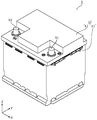
- FIG. 1 is a perspective view showing the appearance of the power storage device according to the embodiment.
- FIG. 2 is an exploded perspective view showing each component when the power storage device according to the embodiment is disassembled.
- FIG. 3 is a perspective view showing the appearance of the power storage element according to the embodiment.
- FIG. 4 is a perspective view showing a bus bar frame according to the embodiment.
- FIG. 5 is a plan view showing a bus bar frame according to the embodiment.
- FIG. 6 is a cross-sectional view showing an assembling structure of the bus bar frame and the sensor according to the embodiment.
- FIG. 7 is a plan view of a part of the power storage device during the bonding step according to the embodiment.
- FIG. 8 is a plan view of a part of the power storage device during the bonding step according to the embodiment.
- the inventor of the present application has found that there are two factors as reasons why the state of the power storage element cannot be accurately detected when the sensor is adhered to the power storage element with an adhesive. The first is that the adhesive is interposed between the sensor and the power storage element, so that the sensor receives the buoyancy from the adhesive and cannot accurately detect the state of the power storage element. The second is that the adhesive is interposed between the sensor and the power storage element, which lowers the thermal conductivity and makes it impossible to accurately detect the state of the power storage element.
- the power storage device is arranged on the power storage element, the sensor attached to the power storage element, and the storage element, and holds the sensor in a state where the detection surface of the sensor is exposed toward the power storage element.
- a member and an exterior body accommodating a power storage element, a sensor, and a holding member are provided, and an adhesive layer for joining the holding member and the power storage element is interposed between the holding member and the power storage element. In plan view, it is arranged at a position that does not overlap the detection surface of the sensor.
- the adhesive layer for joining the holding member and the power storage element is arranged at a position where it does not overlap with the detection surface of the sensor in a plan view, the sensor can detect the buoyancy from the adhesive forming the adhesive layer. It is possible to suppress receiving. Therefore, even if there is no urging portion for pressing the sensor, the contact property of the sensor with respect to the power storage element can be improved.
- the adhesive layer Since the adhesive layer is arranged at a position that does not overlap the detection surface of the sensor in a plan view, the adhesive layer does not intervene on the heat conduction path connecting the power storage element to the detection surface of the sensor, and the heat conduction caused by the adhesive layer. It is unlikely that the rate will drop. In this way, the state of the power storage element can be detected more accurately by improving the contact property and suppressing the decrease in thermal conductivity.
- the detection surface of the sensor projects from the holding member toward the power storage element, and the amount of protrusion from the holding member on the detection surface may be greater than or equal to the thickness of the adhesive layer.
- the amount of protrusion from the holding member on the detection surface of the sensor is equal to or larger than the thickness of the adhesive layer, even if the holding member receives the buoyancy from the adhesive and tries to float from a predetermined position, the detection surface is further affected. It can surely come into contact with the power storage element.
- An opening may be formed on the surface of the holding member facing the adhesive layer on the outer side of the detection surface of the sensor.
- the adhesive layer is formed by applying an adhesive to the power storage element or the holding member and then pressing the power storage element and the holding member in close proximity to each other. At the time of pressing, the adhesive spreads between the power storage element and the holding member. Since the holding member has an opening formed on the outer side of the detection surface, the adhesive approaching the detection surface due to wet spread enters the opening. Therefore, it is possible to prevent the adhesive from spreading in the vicinity of the detection surface. That is, it is possible to more reliably suppress the sensor from receiving the buoyancy due to the adhesive.
- the holding member holds the bus bar connected to the power storage element, the bus bar may be arranged at the end portion of the holding member, and the sensor may be arranged at the central portion of the holding member.
- the holding member In the vicinity of the bus bar, it is desirable to firmly fix the holding member to the power storage element. Therefore, it is necessary to sufficiently apply the adhesive to the end portion of the holding member on which the bus bar is arranged. On the other hand, since the central portion of the holding member is separated from the bus bar, it is possible to reduce the amount of the adhesive applied. Since the sensor is arranged with respect to the central portion of the holding member, even if the adhesive layer is arranged so as to avoid the periphery of the detection surface of the sensor, the fixing of the holding member is not so affected. Therefore, in the holding member, it is possible to improve the contact property of the sensor with respect to the power storage element while firmly fixing the vicinity of the bus bar.
- the sensor has a pair of support portions that sandwich the detection surface, and the support portions may be supported by the holding member.
- the senor since the sensor is supported by the holding member by a pair of support portions sandwiching the detection surface, it is possible to make the sensor difficult to float even if it receives buoyancy from the adhesive. Therefore, the detection surface can be more reliably brought into contact with the power storage element.
- the adhesive layer may be arranged so as to avoid the periphery of the detection surface.
- the adhesive layer is arranged so as to avoid the periphery of the detection surface, the adhesive forming the adhesive layer is less likely to get wet and spread to the detection surface. Therefore, it is possible to more reliably suppress the sensor from receiving the buoyancy due to the adhesive.
- the power storage device is arranged on the power storage element, the sensor attached to the power storage element, and the storage element, and holds the sensor in a state where the detection surface of the sensor is exposed toward the power storage element.
- a member and an exterior body accommodating a power storage element, a sensor, and a holding member are provided, and a heat conductive adhesive layer for joining the sensor and the power storage element is interposed between the detection surface of the sensor and the power storage element.
- the heat conductive adhesive layer for joining the sensor and the power storage element is interposed between the detection surface of the sensor and the power storage element, it is on the heat conduction path connecting the power storage element to the detection surface of the sensor. It is possible to suppress a decrease in thermal conductivity. As a result, the state of the power storage element can be detected more accurately.
- the direction in which the power storage elements are arranged is defined as the X-axis direction.
- the direction in which the electrode terminals are arranged in one power storage element or the direction opposite to the short side surface of the container of the power storage element is defined as the Y-axis direction.
- the alignment direction between the main body and the outer lid of the exterior body of the power storage device, or the vertical direction is defined as the Z-axis direction.
- the Z-axis direction is also the insertion direction when a plurality of power storage elements are inserted into the main body opening of the main body.
- X-axis directions, Y-axis directions, and Z-axis directions are directions that intersect each other (hereinafter, orthogonal to each other in the embodiment).
- the Z-axis direction may not be the vertical direction, but for convenience of explanation, the Z-axis direction will be described below as the vertical direction.
- the plus side in the X-axis direction indicates the arrow direction side of the X-axis
- the minus side in the X-axis direction indicates the side opposite to the plus side in the X-axis direction.
- the Y-axis direction and the Z-axis direction are directions that intersect each other (hereinafter, orthogonal to each other in the embodiment).
- the Z-axis direction may not be the vertical direction, but for convenience of explanation, the Z-axis direction will be described below as the vertical direction.
- the plus side in the X-axis direction indicates the arrow direction side of the X-axis
- the minus side in the X-axis direction indicates the side opposite to the plus
- expressions indicating relative directions or postures such as parallel and orthogonal include cases where they are not strictly the directions or postures.
- the fact that two directions are orthogonal not only means that the two directions are completely orthogonal, but also that they are substantially orthogonal, that is, a difference of, for example, about several percent. It also means to include.
- FIG. 1 is a perspective view showing the appearance of the power storage device 1 according to the embodiment.
- FIG. 2 is an exploded perspective view showing each component when the power storage device 1 according to the embodiment is disassembled.
- the power storage device 1 is a device capable of charging electricity from the outside and discharging electricity to the outside, and has a substantially rectangular parallelepiped shape in the present embodiment.
- the power storage device 1 is a battery module (assembled battery) used for power storage, power supply, and the like.
- the power storage device 1 is used for driving a moving body such as an automobile, a motorcycle, a watercraft, a ship, a snowmobile, an agricultural machine, a construction machine, or a railroad vehicle for an electric railway, or for starting an engine. Used as a battery or the like.
- Examples of the above-mentioned automobiles include electric vehicles (EVs), hybrid electric vehicles (HEVs), plug-in hybrid electric vehicles (PHEVs), and gasoline vehicles.
- Examples of the railway vehicle for the electric railway include a train, a monorail, and a linear motor car.
- the power storage device 1 can also be used as a stationary battery or the like used for home use, a generator, or the like.
- the power storage device 1 includes a power storage element 20 and an exterior body 10 accommodating a plurality of power storage elements 20.
- the exterior body 10 has a main body 11 that accommodates a plurality of power storage elements 20, a bus bar frame 17 that is arranged above the plurality of power storage elements 20, and an outer lid 12 that covers the upper part of the bus bar frame 17.
- the exterior body 10 is a rectangular (box-shaped) container (module case) that constitutes the exterior body of the power storage device 1. That is, the exterior body 10 is a member that fixes a plurality of power storage elements 20 and a bus bar frame 17 and the like at predetermined positions and protects these elements from impacts and the like.
- the main body 11 is a bottomed rectangular tubular member with an open upper portion, and the open portion is the main body opening 111.
- the main body opening 111 has a substantially quadrangular shape in a plan view.
- a pair of bus bars 33 held by the bus bar frame 17 and a connection unit 80 including a control circuit and the like are provided in the main body opening 111 of the main body 11.
- the end plate 39 is housed in the main body opening 111 of the main body 11.
- the outer lid 12 is a rectangular member that closes the main body opening 111 of the main body 11.
- the outer lid 12 is joined to the main body 11 in a state of covering the main body opening 111 of the main body 11.
- the outer lid 12 has an external terminal 91 on the positive electrode side and an external terminal 92 on the negative electrode side.
- the external terminals 91 and 92 are electrically connected to a plurality of power storage elements 20 via the connection unit 80 and the bus bar 33, and the power storage device 1 receives electricity from the outside via the external terminals 91 and 92. It charges and discharges electricity to the outside.
- the external terminals 91 and 92 are formed of a conductive member made of a copper alloy such as brass, or a metal such as copper, aluminum, or an aluminum alloy.
- the main body 11 and the outer lid 12 of the exterior body 10 are made of polycarbonate (PC), polypropylene (PP), polyethylene (PE), polystyrene (PS), polyphenylene sulfide resin (PPS), polyphenylene ether (PPE (including modified PPE)). ), Polyethylene terephthalate (PET), Polybutylene terephthalate (PBT), Polyether ether ketone (PEEK), Tetrafluoroethylene / perfluoroalkyl vinyl ether (PFA), Polytetrafluoroethylene (PTFE), Polyether sulfone (PES) ), ABS resin, or an insulating member such as a composite material thereof, or an insulating coated metal or the like.
- PC polycarbonate
- PP polypropylene
- PE polyethylene
- PS polystyrene
- PPS polyphenylene sulfide resin
- PPE polyphenylene ether
- PPE polyphenylene ether
- PPE including
- the exterior body 10 prevents the power storage element 20 and the like from coming into contact with the external metal member and the like.
- the exterior body 10 may be formed of a conductive member such as a metal as long as the electrical insulating property of the power storage element 20 or the like is maintained.
- the power storage element 20 is a secondary battery (cell battery) capable of charging electricity and discharging electricity, and more specifically, a non-aqueous electrolyte secondary battery such as a lithium ion secondary battery. ..
- the power storage element 20 has a flat rectangular parallelepiped shape (square shape), and in the present embodiment, eight power storage elements 20 are arranged in the X-axis direction. The shape of the power storage element 20 and the number of power storage elements 20 arranged are not limited.
- the power storage element 20 is not limited to the non-aqueous electrolyte secondary battery, and may be a secondary battery other than the non-aqueous electrolyte secondary battery, or may be a capacitor, and the user does not need to charge the battery. It may be a primary battery that can use the stored electricity.
- the power storage element 20 may be a solid electrolyte battery.
- FIG. 3 is a perspective view showing the appearance of the power storage element 20 according to the embodiment.
- the power storage element 20 includes a container 21 and a pair of electrode terminals (positive electrode terminal 221 and negative electrode terminal 222).
- An electrode body, a pair of current collectors (positive electrode side and negative electrode side), an electrolytic solution (non-aqueous electrolyte), and the like are housed inside the container 21, but these are not shown.
- the type of electrolytic solution is not particularly limited as long as it does not impair the performance of the power storage element 20, and various types can be selected.
- Gaskets and the like are arranged between the container 21 and the pair of electrode terminals and the pair of current collectors in order to improve the insulating property and the airtightness, but their illustrations are also omitted.
- spacers arranged on the side or below the electrode body, an insulating film for wrapping the electrode body, and the like may be arranged.
- the container 21 is a rectangular parallelepiped (square or box-shaped) case having a container body 210 having an opening and a lid 220 that closes the opening of the container body 210.
- the container 21 has a structure in which the inside can be sealed by accommodating the electrode body or the like inside the container body 210 and then joining the container body 210 and the lid 220 by welding or the like. ..
- the material of the container 21 is not particularly limited, but it is preferably a weldable metal such as stainless steel, aluminum, aluminum alloy, iron, and galvanized steel sheet.
- the container body 210 is a rectangular cylindrical member having a bottom that constitutes the main body of the container 21, and has an opening formed on the plus side in the Z-axis direction. That is, as shown in FIG. 3, the container body 210 has a pair of long side surfaces 211 on both side surfaces in the X-axis direction, a pair of short side surfaces 212 on both side surfaces in the Y-axis direction, and a minus in the Z-axis direction. It has a bottom surface 213 on the side.
- the lid 220 is a rectangular plate-shaped member constituting the lid portion of the container 21, and is arranged so as to extend in the Y-axis direction on the positive side in the Z-axis direction of the container main body 210.
- the lid 220 is provided with a liquid injection unit (not shown) for injecting an electrolytic solution, a gas discharge valve 29 for discharging gas when the pressure inside the container 21 rises, and releasing the pressure.
- the positive electrode terminal 221 and the negative electrode terminal 222 are formed of a conductive member such as a metal such as aluminum, aluminum alloy, copper or copper alloy, and are provided on the lid 220. Specifically, the positive electrode terminal 221 and the negative electrode terminal 222 are electrode terminals arranged so as to project from the lid 220 of the container 21 toward the bus bar frame 17 side (upward, that is, toward the positive side in the Z-axis direction). be.
- the power storage device 1 charges electricity from the outside and goes to the outside. Can discharge electricity.
- the electrode body is a power storage element (power generation element) formed by laminating a positive electrode plate, a negative electrode plate, and a separator.
- the positive electrode plate is a positive electrode active material layer formed on a positive electrode base material layer which is a current collecting foil made of a metal such as aluminum or an aluminum alloy.
- the negative electrode plate is a negative electrode active material layer formed on a negative electrode base material layer which is a current collecting foil made of a metal such as copper or a copper alloy.
- the active material used for the positive electrode active material layer and the negative electrode active material layer known materials can be appropriately used as long as they can occlude and release lithium ions.
- the electrode body is a wound electrode body formed by winding electrode plates (positive electrode plate and negative electrode plate), and a laminated type (stack type) electrode formed by laminating a plurality of flat plate-shaped electrode plates.
- a wound electrode body formed by winding electrode plates (positive electrode plate and negative electrode plate), and a laminated type (stack type) electrode formed by laminating a plurality of flat plate-shaped electrode plates.
- Any form of electrode body such as a body or a bellows-shaped electrode body obtained by folding a electrode plate into a bellows shape may be used.
- the current collector is a member (positive electrode current collector and negative electrode current collector) having conductivity and rigidity electrically connected to the electrode terminal (positive electrode terminal 221 and the negative electrode terminal 222) and the electrode body.
- the positive electrode current collector is formed of aluminum or an aluminum alloy or the like like the positive electrode base material layer of the positive electrode plate
- the negative electrode current collector is formed of copper or a copper alloy or the like like the negative electrode base material layer of the negative electrode plate.
- the bus bar 33 is arranged on at least two power storage elements 20 while being held by the bus bar frame 17, and is a rectangular plate that electrically connects the positive electrode terminals 221 and the negative electrode terminals 222 of the at least two power storage elements 20. It is a shaped member.
- the bus bar 33 is formed of a conductive member made of metal such as copper, copper alloy, aluminum, aluminum alloy, nickel, and clad material. In the present embodiment, five bus bars 33 are used to connect two power storage elements 20 in parallel to form four sets of power storage element groups, and to connect the four sets of power storage element groups in series. ing.
- the connection unit 80 is a unit having a plurality of bus bars, a control board, and the like, and connects a power storage element group consisting of eight power storage elements 20 to external terminals 91 and 92.
- the control board included in the connection unit 80 has a plurality of electric components, and these plurality of electric components form a detection circuit for detecting the state of each power storage element 20, a control circuit for controlling charging and discharging, and the like. There is.
- the connection unit 80 is provided with a connector portion 89 of a detection circuit or a control circuit. In this embodiment, the connection unit 80 is fixed to the bus bar frame 17.
- the detection circuit and the control circuit may be formed on separate substrates.
- the connection unit 80 does not have to have a control board.
- a control device arranged outside the power storage device 1 may control charging and discharging of each power storage element 20.
- a sensor 81 (see FIG. 4) attached to the power storage element 20 is electrically connected to the detection circuit.
- the sensor 81 is a sensor that detects the state of the power storage element 20.
- examples of the sensor 81 include a temperature sensor (thermistor) that detects the temperature of the power storage element 20, a voltage sensor that detects the voltage of the power storage element 20, and the like.
- the bus bar frame 17 is an example of a holding member arranged above the plurality of power storage elements 20 (the side on which the positive electrode terminal 221 and the negative electrode terminal 222 are arranged).
- the bus bar 33 and the power storage element It is a member that holds the sensor 81 attached to the 20. More specifically, the bus bar frame 17 is a member that holds a plurality of bus bars 33, a connection unit 80, a sensor 81, and other wirings (not shown), and can regulate the positions of these members. be.
- the bus bar frame 17 is provided with a plurality of bus bar openings 17a that hold each of the plurality of bus bars 33 and expose a part of each of the plurality of bus bars 33 to the side of the plurality of power storage elements 20. By being fixed to the main body 11, the bus bar frame 17 also has a role of restricting the movement of the plurality of power storage elements 20 upward (plus side in the Z-axis direction).
- the bus bar frame 17 arranged above the plurality of power storage elements 20 may be referred to as a "bus bar plate", an “inner lid”, or the like.
- the bus bar frame 17 is an insulating member such as PC, PP, PE, PS, PPS, PPE (including modified PPE), PET, PBT, PEEK, PFA, PTFE, PES, ABS resin, or a composite material thereof, or , It is made of insulating coated metal or the like.
- the pair of end plates 39 are rectangular plates arranged at positions in the main body 11 that collectively sandwich a plurality of power storage elements 20. Specifically, the pair of end plates 39 are arranged at positions parallel to the YZ plane and sandwiching the plurality of power storage elements 20 in the X-axis direction. That is, the pair of end plates 39 are arranged so as to overlap with the long side surface 211 of the container 21 of the power storage element 20 arranged on the outermost side.
- the end plate 39 is made of an insulating coated metal or the like.
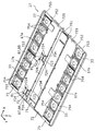
- FIG. 4 is a perspective view showing the bus bar frame 17 according to the embodiment. Specifically, FIG. 4 is a perspective view of the bus bar frame 17 as viewed from below.
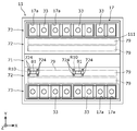
- FIG. 5 is a plan view showing the bus bar frame 17 according to the embodiment, and shows a state before application of the adhesive. Specifically, FIG. 5 is a view of the outer lid 12 and the bus bar frame 17 as viewed from below, and shows the state after the adhesive is applied.
- FIG. 6 is a cross-sectional view showing an assembling structure of the bus bar frame 17 and the sensor 81 according to the embodiment. Specifically, FIG. 6 is a cross-sectional view of the cut surface including the VV line in FIG.
- the bus bar frame 17 has a gas path portion 71, an adhesive portion 72, and a bus bar installation portion 73, which are partitioned by a plurality of pairs of ribs 751 to 753. There is.
- the gas path portion 71 is arranged in the central portion of the bus bar frame 17 in the Y-axis direction, and is a portion extending in the X-axis direction.
- the gas path portion 71 is a path for gas discharged from the gas discharge valve 29 of the power storage element 20.
- the adhesive portion 72 is a pair of portions that sandwich the gas path portion 71 in the Y-axis direction, and each extends in the X-axis direction.
- the adhesive portion 72 includes an adhesive region 721 and a sensor region 722.
- An adhesive layer 79 (shown by dot hatching in FIG. 5) for adhering the bus bar frame 17 and the plurality of power storage elements 20 is laminated (coated) on the adhesive region 721. That is, the surface of the adhesive portion 72 is a surface facing the adhesive layer 79.
- the sensor area 722 is an area where the detection surface 87 of the sensor 81 is exposed. In FIG. 5, the sensor area 722 is indicated by a dashed rectangle. Assuming that the total length of the bus bar frame 17 in the Y-axis direction is L, the sensor region 722 is arranged closer to the center than L / 4 from the end on the minus side in the Y-axis direction of the bus bar frame 17. Two sensor regions 722 are provided with respect to the adhesive portion 72 on the negative side in the Y-axis direction of the pair of adhesive portions 72.
- One sensor region 722 corresponds to the power storage element 20 located on the minus side in the X-axis direction, and the other sensor area 722 corresponds to the fourth power storage element 20 from the end on the plus side in the X-axis direction.
- the two sensor regions 722 are separated in the X-axis direction in which the plurality of power storage elements 20 are arranged.
- the sensor region 722 is provided with a first opening 723 that exposes the detection surface 87 of the sensor 81, and a plurality of second openings 724 arranged around the first opening 723.
- the entire sensor region 722 includes the entire first opening 723 and the entire second opening 724.
- the first opening 723 is located in the center and the plurality of second openings 724 are located near the boundary of the sensor region 722.
- the two sensor regions 722 are arranged in the adhesive portion 72 on the minus side in the Y-axis direction with respect to the gas path portion 71.
- the two sensor regions 722 are arranged on the minus side in the Y-axis direction with respect to the center in the Y-axis direction of the bus bar frame 17.
- the connector portion 89 of the detection circuit or the control circuit included in the connection unit 80 is arranged on the minus side in the Y-axis direction with respect to the center in the Y-axis direction of the connection unit 80.
- Wiring (not shown) derived from the sensor 81 (sensor body 82) arranged in the sensor region 722 is electrically connected to the connector portion 89.
- the connector portion 89 is arranged so that the terminal portion to which the wiring of the sensor 81 is connected faces the minus side in the Y-axis direction.
- the connection unit 80 is arranged at substantially the center of the bus bar frame 17 in the Z-axis direction, and the connector portion 89 is arranged at the substantially center of the bus bar frame 17 in the X-axis direction.
- Both the connector portion 89 of the connection unit 80 and the sensor area 722 are arranged so as to be aligned with the minus side in the Y-axis direction from the center in the Y-axis direction of the bus bar frame 17.
- the wiring (not shown) derived from the sensor 81 (sensor body 82) can be arranged on the same negative side in the Y-axis direction as the connector portion 89. Therefore, it is not necessary to route the wiring derived from the sensor 81 extra. That is, the wiring can be easily connected to the detection circuit of the connection unit 80 while suppressing the lengthening of the wiring.
- the sensor region 722 is not arranged in the adhesive portion 72 on the positive side in the Y-axis direction with respect to the gas path portion 71. Therefore, in the adhesive portion 72 on the positive side in the Y-axis direction with respect to the gas path portion 71, the adhesive layer 79 is arranged over the entire area from one end side to the other end side in the X-axis direction.
- the first opening 723 has an opening shape corresponding to the plan view shape of the detection surface 87.
- the second opening 724 has an opening shape smaller than that of the first opening 723.
- the second opening 724 is arranged around the first opening 723. Specifically, as shown in FIG. 6, the second opening 724 is arranged in the vicinity of the first opening 723 at intervals shorter than the length of the first opening 723 in the Y-axis direction. More preferably, the second opening 724 is arranged in the vicinity of the first opening 723 at intervals shorter than the length of the second opening 724 in the Y-axis direction.
- the bus bar installation portion 73 is a pair of portions that sandwich the gas path portion 71 and the pair of adhesive portions 72 in the Y-axis direction, and each extends in the X-axis direction.
- the bus bar installation portion 73 is arranged within a range from both ends of the bus bar frame 17 in the Y-axis direction to L / 4.
- the bus bar installation unit 73 is a portion where a plurality of bus bars 33 are installed.
- the bus bar installation portion 73 is formed with a plurality of bus bar openings 17a that expose locations connected to the power storage element 20 in each bus bar 33.
- a plurality of pairs of ribs 751 to 753 are erected from the inner surface of the bus bar frame 17 and extend in the X-axis direction.
- the tips of the plurality of pairs of ribs 751 to 753 abut on the lid 220 of the container 21 in the power storage element 20, respectively.
- the plurality of pairs of ribs 751 to 753 have a function of improving the strength of the bus bar frame 17.
- the pair of ribs 751 and the pair of ribs 752 also function as a portion that regulates the position of the adhesive layer 79. Specifically, as shown in FIGS.
- a pair of ribs 751 are arranged on the bus bar frame 17 at positions sandwiching the gas path portion 71 in the Y-axis direction.
- each of the pair of ribs 752 is arranged at a position where the adhesive portion 72 is sandwiched together with the pair of ribs 751.
- each of the pair of ribs 753 is arranged at a position sandwiching the bus bar installation portion 73 together with the pair of ribs 752. That is, one of the pair of ribs 753 is arranged at the end on the minus side in the Y-axis direction in the bus bar frame 17, and the other of the pair of ribs 753 is arranged at the end on the plus side in the Y-axis direction in the bus bar frame 17. There is.
- a plurality of recesses 754 are provided in the plurality of pairs of ribs 751 to 753.
- the plurality of recesses 754 are provided at positions corresponding to the edges of the power storage elements 20.
- An insulating film may be wound around the power storage element 20 in order to insulate the power storage element 20 adjacent to the power storage element 20. A part of this insulating film may protrude from the upper end of the container 21 when it is wound around the container 21 of the power storage element 20. Since a part of the insulating film protruding from the upper end of the container 21 is housed in the recesses 754 of the ribs 751 to 753, interference between the insulating film and the bus bar frame 17 is suppressed.
- the sensor 81 includes a sensor main body 82 and a mounting member 83.
- the sensor body 82 is a portion that detects the state of the power storage element 20.
- the sensor body 82 is formed in a rectangular shape in a plan view, and its outer surface is a detection surface 821.
- the sensor body 82 is provided with wiring (not shown) connected to the detection circuit of the connection unit 80.
- the sensor body 82 has a substantially rectangular parallelepiped shape that is long in the X-axis direction. That is, the sensor main body 82 is arranged so that the X-axis direction is the longitudinal direction. Then, the wiring derived from the sensor main body 82 is derived from the end portion of the sensor main body 82 in the X-axis direction along the X-axis direction. As described above, the sensor main body 82 is arranged in each sensor area 722 shown in FIG. The wiring derived from the end portion of the sensor body 82 in the X-axis direction is connected to the connector portion 89 in a state along the X-axis direction toward the connector portion 89 arranged in the central portion of the bus bar frame 17. Will be done. As a result, it is not necessary to route the wiring extra, and it can be easily connected to the detection circuit of the connection unit 80.
- the mounting member 83 is a member for mounting the sensor main body 82 to the bus bar frame 17.
- the mounting member 83 is preferably made of a member having a relatively high thermal conductivity.
- the mounting member 83 can be used by bending a metal plate material.
- the mounting member 83 integrally includes the accommodating portion 84 and the pair of supporting portions 85, and has substantially the same size as the sensor main body 82 in the X-axis direction.
- the accommodating portion 84 is a portion accommodating the sensor main body 82, and is formed in a substantially U shape when viewed in the X-axis direction.
- the detection surface 821 of the sensor body 82 is in contact with the inner bottom surface of the accommodating portion 84.
- a heat conductive sheet 88 having a relatively high thermal conductivity is laminated on the outer bottom surface of the accommodating portion 84.
- the outer surface of the heat conductive sheet 88 is in contact with the lid 220 of the power storage element 20.
- the heat from the power storage element 20 can be reliably transferred to the detection surface 821 of the sensor body 82 via the heat conductive sheet 88 and the mounting member 83. That is, it can be said that the outer surface of the heat conductive sheet 88 is the detection surface 87 of the sensor 81.
- the heat conductive sheet 88 may be made of resin or metal as long as it has insulating properties.
- the heat conductive sheet 88 is not in contact with the adhesive layer 79 and is separated from the adhesive layer 79 in the planes in the X-axis direction and the Y-axis direction.
- the adhesive layer 79 is arranged between the sensor body 82 and the power storage element 20 in the X-axis direction.
- the pair of support portions 85 extend outward along the Y-axis direction from each of both end portions of the accommodating portion 84. Each of the pair of support portions 85 is supported with respect to the bus bar frame 17. Specifically, the pair of support portions 85 are fixed to the upper portion of the bus bar frame 17 by adhesion, welding, welding, mechanical joining, or the like.
- the entire detection surface 87 (outer surface of the heat conductive sheet 88) of the sensor 81 is exposed by the first opening 723 of the sensor region 722.
- the detection surface 87 projects from the sensor region 722 of the bus bar frame 17 toward the power storage element 20.
- the amount of protrusion H1 from the bus bar frame 17 (the amount of discharge from the surface of the sensor region 722) on the detection surface 87 is equal to or greater than the thickness t1 of the adhesive layer 79.
- the detection surface 87 of the sensor 81 is in contact with the surface of the lid 220 of the power storage element 20. As shown in FIG.
- the adhesive layer 79 is arranged at a position that does not overlap the detection surface 87 in a plan view, avoiding the periphery of the detection surface 87 and the detection surface 87.
- the plan view means viewing from the normal direction (Z-axis direction) of the surface of the lid 220 to which the adhesive layer 79 is attached.
- the case where the sensor 81 is provided with the heat conductive sheet 88 is illustrated, but the sensor 81 may not be provided with the heat conductive sheet 88.
- the outer bottom surface of the accommodating portion 84 of the mounting member 83 can be used as the detection surface of the sensor 81.
- the detection surface 821 shall be the detection surface of the sensor 81. Is also possible.
- FIG. 7 and 8 are plan views of a part of the power storage device 1 at the time of the bonding process according to the embodiment.
- FIG. 7 is a plan view showing the inside of the main body 11 of the exterior body 10 in which the plurality of power storage elements 20 are housed.
- FIG. 8 is a plan view showing a state in which the bus bar frame 17 is adhered to the plurality of power storage elements 20.
- the adhesive layer 79 is illustrated by dot hatching
- FIG. 8 the outer shape of the adhesive layer 79 is illustrated by a alternate long and short dash line.
- a plurality of power storage elements 20 are housed in a main body opening 111 of the main body 11 in a state of being sandwiched between a pair of end plates 39.
- the bottom surface 213 of the container 21 opposite to the lid 220 of the container 21 in the Z-axis direction and the inner surface of the main body 11 facing the bottom surface 213 of the container 21 in the Z-axis direction are adhesives. Is fixed by. The bonding process is executed in this state. That is, the plurality of power storage elements 20 are fixed to the main body 11 by an adhesive, and further fixed to the bus bar frame 17 by an adhesive.
- the plurality of power storage elements 20 sandwich an adhesive layer between the main body 11 and the bus bar frame 17, respectively.
- an adhesive is applied to the lid 220 of each container 21 of the plurality of power storage elements 20 by a dispenser or the like to form an adhesive layer 79.
- the adhesive include an adhesive made of silicone as a material.
- the adhesive is applied so as to avoid a portion corresponding to each sensor region 722 (shown by a broken line rectangle in FIG. 7).
- the portion is referred to as a non-coated region R10.
- the non-coated region R10 avoids the first opening 723 in the central portion of each sensor region 722, that is, the detection surface 87 of the sensor 81, and the adhesive is applied.
- the plurality of bus bars 33 and the bus bar frame 17 are assembled to the bus bar frame 17 and integrated, and the adhesive layer 79 is sandwiched between the plurality of bus bars 33 and the plurality of power storage elements 20. It is attached (see FIGS. 6 and 8). At this time, the bus bar frame 17 is pressed against the adhesive layers 79 on the plurality of power storage elements 20. At the time of this pressing, the adhesive layer 79 is pressed by the bus bar frame 17, so that it is expanded more than the state immediately after application.
- the spread of the spread adhesive layer 79 is restricted by the ribs 751 and 752.
- the adhesive layer 79 also enters the non-coated region R10 by spreading, but it is difficult to reach the detection surface 87 (first opening 723) of the sensor 81 arranged at the center thereof (1st opening 723). (See FIG. 6).
- the adhesive layer 79 that has entered the non-coated region R10 enters the second opening 724 and has a more detection surface. It is difficult to reach 87.
- the adhesive layer 79 is arranged at a position where it does not overlap the detection surface 87 of the sensor 81 in a plan view, the sensor 81 receives the buoyancy from the adhesive forming the adhesive layer 79. Can be suppressed.
- the adhesive layer 79 is cured while applying a pressing force toward the plurality of power storage elements 20 to the bus bar frame 17. Since the pressing force also acts on the sensor 81 during curing, it is possible to more reliably prevent the detection surface 87 of the sensor 81 from floating from the power storage element 20.
- the strength of the bus bar frame 17 is enhanced by a plurality of pairs of ribs 751 to 753. Therefore, even if a pressing force acts on the bus bar frame 17, the bus bar frame 17 is unlikely to be deformed. That is, it is also suppressed that the sensor 81 floats from the power storage element 20 due to the deformation of the bus bar frame 17.
- FIG. 6 shows a case where the protrusion amount H1 of the detection surface 87 and the thickness t1 of the adhesive layer 79 are equivalent after curing.
- the adhesive layer 79 is avoided from the periphery of the detection surface 87, that is, the periphery of the first opening 723, elastic deformation is possible around the first opening 723 of the bus bar frame 17.
- the protrusion amount H1 of the detection surface 87 is larger than the thickness t1 of the adhesive layer 79
- the bus bar frame 17 is elastically deformed, and the difference can be absorbed.
- the restoring force of the bus bar frame 17 acts on the detection surface 87, so that the detection surface 87 can be more reliably brought into contact with the power storage element 20.
- the bonding step according to the present embodiment, the case where the adhesive is applied to the lid 220 of each container 21 of the plurality of power storage elements 20 to form the adhesive layer 79 is illustrated. However, in the bonding step, an adhesive may be applied to the bus bar frame 17 to form the bonding layer 79.
- the positive electrode terminals 221 and the negative electrode terminals 222 of the plurality of power storage elements 20 can be connected to the plurality of bus bars 33, or the outer edge of the bus bar frame 17 is separated from the adhesive layer 79.
- the portion and the main body portion 11 are fixed by heat caulking.
- the connection unit 80 is arranged on the positive side of the bus bar frame 17 in the Z-axis direction.
- the wiring for temperature measurement of the sensor 81 and the wiring for voltage measurement connected to the plurality of bus bars 33 are connected to the connector portion 89 of the connection unit 80.
- the outer lid 12 is assembled to the main body 11 by melting a part of the main body 11 made of resin as well as a part of the outer lid 12 made of resin by heat and pressing the melted parts against each other.
- the power storage element 20, the sensor 81 attached to the power storage element 20, and the detection surface 87 of the sensor 81 are arranged on the power storage element 20.
- a bus bar frame 17 (holding member) for holding the sensor 81 in a state of being exposed toward 20, and an exterior body 10 for accommodating the power storage element 20, the sensor 81, and the bus bar frame 17, are provided, and the bus bar frame 17 and the power storage element 20 are provided.
- An adhesive layer 79 that joins the bus bar frame 17 and the power storage element 20 is interposed between the adhesive layer 79, and the adhesive layer 79 is arranged at a position that does not overlap the detection surface 87 of the sensor 81 in a plan view.
- the adhesive layer 79 for joining the bus bar frame 17 and the power storage element 20 is arranged at a position where the sensor 81 does not overlap the detection surface 87 in a plan view, the adhesive forming the adhesive layer 79 is formed. It is possible to prevent the sensor 81 from directly receiving the buoyancy from the sensor 81. Therefore, even if there is no urging portion for pressing the sensor 81, the contact property of the sensor 81 with respect to the power storage element 20 can be improved. As described above, with a simple structure, the contact property of the sensor 81 with respect to the power storage element 20 can be improved.
- the adhesive layer 79 is arranged so as to avoid the periphery of the detection surface 87, the adhesive forming the adhesive layer 79 is less likely to get wet and spread to the detection surface 87. Therefore, it is possible to more reliably suppress the sensor 81 from receiving the buoyancy due to the adhesive.
- the adhesive layer 79 Since the adhesive layer 79 is arranged at a position that does not overlap the detection surface 87 of the sensor 81 in a plan view, the adhesive layer 79 does not intervene on the heat conduction path connecting the power storage element 20 to the detection surface of the sensor 81. The decrease in thermal conductivity due to the adhesive layer 79 is unlikely to occur. In this way, the state of the power storage element 20 can be detected more accurately by improving the contact property and suppressing the decrease in thermal conductivity.
- the detection surface 87 of the sensor 81 projects from the bus bar frame 17 toward the power storage element 20, and the amount H1 protruding from the bus bar frame 17 on the detection surface 87 is equal to or greater than the thickness t1 of the adhesive layer 79.
- the bus bar frame 17 since the amount of protrusion H1 from the bus bar frame 17 on the detection surface 87 of the sensor 81 is equal to or greater than the thickness t1 of the adhesive layer 79, the bus bar frame 17 receives buoyancy from the adhesive and floats from a predetermined position. Even if this is done, the detection surface 87 can be more reliably brought into contact with the power storage element 20.
- a second opening 724 (opening) is formed on the surface of the bus bar frame 17 facing the adhesive layer 79 on the outer side of the detection surface 87 of the sensor 81.
- the adhesive layer 79 is formed by applying an adhesive to the power storage element 20 or the bus bar frame 17 and then pressing the power storage element 20 and the bus bar frame 17 in close proximity to each other. At the time of pressing, the adhesive spreads between the power storage element 20 and the bus bar frame 17. Since the bus bar frame 17 has a second opening 724 formed on the outer side of the detection surface 87, the adhesive approaching the detection surface 87 due to wet spread enters the second opening 724. Therefore, it is possible to prevent the adhesive from spreading in the vicinity of the detection surface 87. That is, it is possible to more reliably suppress the sensor 81 from receiving the buoyancy due to the adhesive.
- the bus bar frame 17 holds a bus bar 33 connected to the power storage element 20, the bus bar 33 is arranged at the end of the bus bar frame 17, and the sensor 81 is arranged at the center of the bus bar frame 17.
- the bus bar frame 17 In the vicinity of the bus bar 33, it is desired that the bus bar frame 17 is firmly fixed to the power storage element 20. Therefore, it is necessary to sufficiently apply the adhesive to the end portion of the bus bar frame 17 on which the bus bar 33 is arranged. On the other hand, since the central portion of the holding member is separated from the bus bar 33, it is possible to reduce the amount of the adhesive applied. Since the sensor 81 is arranged with respect to the central portion of the bus bar frame 17, even if the adhesive layer 79 is arranged avoiding the periphery of the detection surface 87 of the sensor 81, the fixing of the bus bar frame 17 is not so affected. Not reachable. Therefore, in the bus bar frame 17, it is possible to improve the contact property of the sensor 81 with respect to the power storage element 20 while firmly fixing the vicinity of the bus bar 33.
- the sensor region 722 is arranged closer to the center than L / 4 from the end on the minus side in the Y-axis direction of the bus bar frame 17, and L / from both ends in the Y-axis direction of the bus bar frame 17.
- the bus bar installation portion 73 is arranged within the range up to 4.
- the sensor 81 can be reliably arranged in the central portion of the bus bar frame 17 simply by arranging the sensor 81 in the sensor region 722, and the bus bar 33 can be placed in the bus bar 33 simply by installing the bus bar 33 in the bus bar installation portion 73. It can be reliably placed at the end of the frame 17.
- the sensor 81 has a pair of support portions 85 that sandwich the detection surface 87, and the support portions 85 are supported by the bus bar frame 17.
- the senor 81 since the sensor 81 is supported by the bus bar frame 17 by a pair of support portions 85 sandwiching the detection surface 87, the sensor 81 can be made difficult to float even if it receives buoyancy from the adhesive. Therefore, the detection surface 87 can be more reliably brought into contact with the power storage element 20.
- the bus bar frame 17 is exemplified as an example of the holding member that holds the sensor 81.
- a member other than the bus bar frame 17 can be adopted as the holding member.
- the adhesive layer 79 is arranged avoiding the periphery of the detection surface 87 of the sensor 81 is illustrated, but the adhesive layer 79 is arranged at a position where it does not overlap only with the detection surface 87 in a plan view. It may have been done. That is, the adhesive layer 79 may be arranged so as to avoid only the detection surface 87.
- the thermal conductive adhesion is made between the detection surface 87 of the sensor 81 and the power storage element 20. Layers may intervene. Specifically, for example, it can be realized by changing the heat conductive sheet 88 shown in FIG. 6 to a heat conductive adhesive layer.
- the heat conductive adhesive layer is not included in the sensor 81, but is a portion for joining the sensor 81 and the power storage element 20.
- the thermally conductive adhesive layer is formed of an adhesive having a thermal conductivity higher than that of the adhesive layer 79.
- the thermally conductive adhesive layer may be formed of an adhesive having a thermal conductivity equal to or higher than the thermal conductivity of the mounting member 83.
- the heat conductive adhesive layer may be formed of an adhesive having a thermal conductivity equal to or higher than the thermal conductivity of the container 21 of the power storage element 20.
- the heat conductive adhesive layer for joining the sensor 81 and the power storage element 20 is interposed between the detection surface 87 of the sensor 81 and the power storage element 20, the detection surface of the sensor 81 from the power storage element 20 is interposed. It is possible to suppress a decrease in the thermal conductivity on the heat conduction path connecting the 87. As a result, the state of the power storage element 20 can be detected more accurately.
- the adhesive layer 79 may not be present.
- the second opening 724 may be one or is provided. It does not have to be.
- the case where the sensor 81 is arranged at the center of the bus bar frame 17 is illustrated, but the sensor 81 may be arranged at the end of the bus bar frame 17.
- a sensor 81 having a pair of support portions 85 is illustrated.
- the sensor 81 may be provided with at least one support portion 85.
- the power storage device 1 having a plurality of power storage elements 20 is illustrated, but the power storage device including one power storage element may be used.
- the present invention can be applied to a power storage device provided with a power storage element such as a lithium ion secondary battery.
Landscapes
- Engineering & Computer Science (AREA)
- Power Engineering (AREA)
- Chemical & Material Sciences (AREA)
- Chemical Kinetics & Catalysis (AREA)
- Electrochemistry (AREA)
- General Chemical & Material Sciences (AREA)
- Microelectronics & Electronic Packaging (AREA)
- Manufacturing & Machinery (AREA)
- Aviation & Aerospace Engineering (AREA)
- Battery Mounting, Suspending (AREA)
- Connection Of Batteries Or Terminals (AREA)
- Electric Double-Layer Capacitors Or The Like (AREA)
Abstract
蓄電装置(1)は、蓄電素子(20)と、蓄電素子(20)に取り付けられるセンサ(81)と、蓄電素子(20)上に配置され、センサ(81)の検出面(821)が蓄電素子(20)に向けて露出した状態で、センサ(81)を保持するバスバーフレーム(17)と、蓄電素子(20)、センサ(81)及びバスバーフレーム(17)を収容する外装体(10)とを備え、バスバーフレーム(17)と蓄電素子(20)との間には、バスバーフレーム(17)及び蓄電素子(20)を接合する接着層(79)が介在しており、接着層(79)は、平面視において、センサ(81)の検出面(821)に重ならない位置に配置されている。
Description
本発明は、蓄電素子に取り付けられるセンサを備えた蓄電装置に関する。
従来、蓄電素子と、蓄電素子を収容する外装体と、外装体に収容されて、蓄電素子に接続されるバスバーを保持する保持部材とを備えた蓄電装置が知られている。このような蓄電装置には、蓄電素子の状態を検出するためのセンサ(サーミスタ)が設けられており、このセンサが、保持部材によって蓄電素子に押圧された状態で固定されている。(例えば、特許文献1参照)。
ところで、上述した蓄電装置であると、センサを保持しつつ蓄電素子に押圧する構造を採用しているが、当該構造を簡便化すべく、近年においては接着剤でセンサを蓄電素子に接着する方法も検討されている。しかしながら、接着剤によってセンサを蓄電素子に接着する場合には、その接着剤を起因として蓄電素子の状態を正確に検出できないおそれがある。
本発明は、蓄電素子の状態をより正確に検出できる蓄電装置を提供することを目的とする。
本発明の一態様に係る蓄電装置は、蓄電素子と、蓄電素子に取り付けられるセンサと、蓄電素子上に配置され、センサの検出面が蓄電素子に向けて露出した状態で、センサを保持する保持部材と、蓄電素子、センサ及び保持部材を収容する外装体とを備え、保持部材と蓄電素子との間には、保持部材及び蓄電素子を接合する接着層が介在しており、接着層は、平面視において、センサの検出面に重ならない位置に配置されている。
これによれば、センサの検出面に対して平面視で重ならない位置に、保持部材と蓄電素子とを接合する接着層が配置されているので、蓄電素子の状態をより正確に検出できる。
本発明の一態様に係る蓄電装置は、蓄電素子と、蓄電素子に取り付けられるセンサと、蓄電素子上に配置され、センサの検出面が蓄電素子に向けて露出した状態で、センサを保持する保持部材と、蓄電素子、センサ及び保持部材を収容する外装体とを備え、センサの検出面と蓄電素子との間には、センサ及び蓄電素子を接合する熱伝導性接着層が介在している。
これによれば、センサの検出面と蓄電素子との間には、センサ及び蓄電素子を接合する熱伝導性接着層が介在しているので、蓄電素子の状態をより正確に検出できる。
本発明における蓄電装置によれば、蓄電素子の状態をより正確に検出できる。
本願発明者は、接着剤によってセンサを蓄電素子に接着する場合に、蓄電素子の状態を正確に検出できない理由として2つの要因があることを見出した。1つ目は、センサと蓄電素子との間に接着剤が介在することによりセンサが接着剤からの浮力を受けて、蓄電素子の状態を正確に検出できなくすることである。2つ目は、センサと蓄電素子との間に接着剤が介在することで、熱伝導率が低下し、蓄電素子の状態を正確に検出できなくすることである。
本発明の一態様に係る蓄電装置は、蓄電素子と、蓄電素子に取り付けられるセンサと、蓄電素子上に配置され、センサの検出面が蓄電素子に向けて露出した状態で、センサを保持する保持部材と、蓄電素子、センサ及び保持部材を収容する外装体とを備え、保持部材と蓄電素子との間には、保持部材及び蓄電素子を接合する接着層が介在しており、接着層は、平面視において、センサの検出面に重ならない位置に配置されている。
これによれば、センサの検出面に対して平面視で重ならない位置に、保持部材と蓄電素子とを接合する接着層が配置されているので、接着層をなす接着剤からの浮力をセンサが受けてしまうことを抑制できる。したがって、センサを押さえつけるための付勢部などがなくとも、蓄電素子に対するセンサの当接性を高めることができる。
接着層は、平面視においてセンサの検出面に重ならない位置に配置されているので、蓄電素子からセンサの検出面を結ぶ熱伝導路上に接着層が介在せず、接着層を起因とした熱伝導率の低下も発生しにくい。このように、当接性の向上と熱伝導率低下の抑制化とにより、蓄電素子の状態をより正確に検出できる。
センサの検出面は、保持部材から蓄電素子に向けて突出しており、検出面における保持部材からの突出量は、接着層の厚み以上であってもよい。
これによれば、センサの検出面における保持部材からの突出量が、接着層の厚み以上であるので、保持部材が接着剤からの浮力を受けて所定の位置から浮こうとしても検出面をより確実に蓄電素子に当接できる。
保持部材における接着層に対向する面には、センサの検出面よりも外方に開口部が形成されていてもよい。
接着層は、蓄電素子もしくは保持部材に対して接着剤を塗布してから、蓄電素子及び保持部材を近接させて押し付けることで形成される。押し付け時においては蓄電素子及び保持部材間で接着剤が濡れ広がる。保持部材には、検出面よりも外方に開口部が形成されているので、濡れ広がりにより検出面に近づく接着剤は開口部内に進入する。このため、検出面の近傍に接着剤が濡れ広がることを抑制できる。つまり、接着剤による浮力をセンサが受けてしまうことをより確実に抑制できる。
保持部材は、蓄電素子に接続されるバスバーを保持し、バスバーは、保持部材における端部に配置されていて、センサは、保持部材における中央部に配置されていてもよい。
バスバーの近傍においては、保持部材を蓄電素子に強固に固定しておくことが望まれる。このため、バスバーが配置された保持部材の端部においては、接着剤を十分に塗布しておく必要がある。一方、保持部材の中央部においてはバスバーから離れているために、接着剤の塗布量を抑えることも可能である。この保持部材の中央部に対してセンサが配置されているので、センサの検出面の周囲から接着層が回避して配置されていても、保持部材の固定にそれほど影響を及ぼさない。したがって、保持部材において、バスバーの近傍を強固に固定しつつも、蓄電素子に対するセンサの当接性を高めることが可能である。
センサは、検出面を挟む一対の支持部を有し、支持部は、保持部材に支持されていてもよい。
これによれば、センサは、検出面を挟む一対の支持部により保持部材に支持されているので、接着剤からの浮力を受けたとしてもセンサを浮きにくくすることができる。したがって、検出面をより確実に蓄電素子に当接できる。
接着層は、検出面の周囲を回避して配置されていてもよい。
これによれば、接着層が検出面の周囲を回避して配置されているので、接着層をなす接着剤が検出面まで濡れ広がりにくくなる。したがって、接着剤による浮力をセンサが受けてしまうことをより確実に抑制できる。
本発明の一態様に係る蓄電装置は、蓄電素子と、蓄電素子に取り付けられるセンサと、蓄電素子上に配置され、センサの検出面が蓄電素子に向けて露出した状態で、センサを保持する保持部材と、蓄電素子、センサ及び保持部材を収容する外装体とを備え、センサの検出面と蓄電素子との間には、センサ及び蓄電素子を接合する熱伝導性接着層が介在している。
これによれば、センサの検出面と蓄電素子との間には、センサ及び蓄電素子を接合する熱伝導性接着層が介在しているので、蓄電素子からセンサの検出面を結ぶ熱伝導路上の熱伝導率が低下してしまうことを抑制できる。これにより、蓄電素子の状態をより正確に検出できる。
以下、図面を参照しながら、本発明の実施の形態に係る蓄電装置について説明する。以下で説明する実施の形態は、いずれも包括的または具体的な例を示すものである。以下の実施の形態で示される数値、形状、材料、構成要素、構成要素の配置位置及び接続形態などは、一例であり、本発明を限定する主旨ではない。各図において、寸法等は厳密に図示したものではない。
以下の説明及び図面中において、蓄電素子の並び方向、蓄電素子の容器の長側面の対向方向、または、当該容器の厚さ方向をX軸方向と定義する。1つの蓄電素子における電極端子の並び方向、または、蓄電素子の容器の短側面の対向方向をY軸方向と定義する。蓄電装置の外装体における本体部と外蓋との並び方向、または、上下方向をZ軸方向と定義する。Z軸方向は、本体部の本体開口部に対して複数の蓄電素子を挿入する際の挿入方向でもある。これらX軸方向、Y軸方向及びZ軸方向は、互いに交差(以下実施の形態では、直交)する方向である。使用態様によってはZ軸方向が上下方向にならない場合も考えられるが、以下では説明の便宜のため、Z軸方向を上下方向として説明する。以下の説明において、例えば、X軸方向プラス側とは、X軸の矢印方向側を示し、X軸方向マイナス側とは、X軸方向プラス側とは反対側を示す。Y軸方向及びZ軸方向についても同様である。さらに、平行及び直交などの、相対的な方向または姿勢を示す表現は、厳密には、その方向または姿勢ではない場合も含む。例えば、2つの方向が直交している、とは、当該2つの方向が完全に直交していることを意味するだけでなく、実質的に直交していること、すなわち、例えば数%程度の差異を含むことも意味する。
[蓄電装置の全般的な説明]
図1及び図2を用いて、実施の形態に係る蓄電装置1の全般的な説明を行う。図1は、実施の形態に係る蓄電装置1の外観を示す斜視図である。図2は、実施の形態に係る蓄電装置1を分解した場合の各構成要素を示す分解斜視図である。
図1及び図2を用いて、実施の形態に係る蓄電装置1の全般的な説明を行う。図1は、実施の形態に係る蓄電装置1の外観を示す斜視図である。図2は、実施の形態に係る蓄電装置1を分解した場合の各構成要素を示す分解斜視図である。
蓄電装置1は、外部からの電気を充電し、また外部へ電気を放電できる装置であり、本実施の形態では、略直方体形状を有している。蓄電装置1は、電力貯蔵用途または電源用途等に使用される電池モジュール(組電池)である。具体的には、蓄電装置1は、自動車、自動二輪車、ウォータークラフト、船舶、スノーモービル、農業機械、建設機械、または、電気鉄道用の鉄道車両等の移動体の駆動用またはエンジン始動用等のバッテリ等として用いられる。上記の自動車としては、電気自動車(EV)、ハイブリッド電気自動車(HEV)、プラグインハイブリッド電気自動車(PHEV)及びガソリン自動車が例示される。上記の電気鉄道用の鉄道車両としては、電車、モノレール及びリニアモーターカーが例示される。蓄電装置1は、家庭用または発電機用等に使用される定置用のバッテリ等としても用いることができる。
図1及び図2に示すように、蓄電装置1は、蓄電素子20と、複数の蓄電素子20を収容する外装体10とを備える。外装体10は、複数の蓄電素子20を収容する本体部11と、複数の蓄電素子20の上方に配置されるバスバーフレーム17と、バスバーフレーム17の上方を覆う外蓋12とを有する。
外装体10は、蓄電装置1の外装体を構成する矩形状(箱状)の容器(モジュールケース)である。つまり、外装体10は、複数の蓄電素子20及びバスバーフレーム17等を所定の位置に固定し、これら要素を衝撃などから保護する部材である。
本体部11は、上部が開放された有底矩形筒状の部材であり、その開放部分が本体開口部111である。本体開口部111は、平面視において略四角形状である。本体部11の本体開口部111内には、複数の蓄電素子20、バスバーフレーム17に加えて、バスバーフレーム17に保持された複数のバスバー33と、制御回路等を含む接続ユニット80と、一対のエンドプレート39とが収容されている。
外蓋12は、本体部11の本体開口部111を閉塞する矩形状の部材である。外蓋12は、本体部11の本体開口部111を覆った状態で本体部11に接合されている。外蓋12は、正極側の外部端子91及び負極側の外部端子92を有している。外部端子91及び92は、接続ユニット80及びバスバー33を介して複数の蓄電素子20と電気的に接続されており、蓄電装置1は、この外部端子91及び92を介して、外部からの電気を充電し、また外部へ電気を放電する。外部端子91及び92は、真鍮などの銅合金、銅、アルミニウム、アルミニウム合金等の金属製の導電部材で形成されている。
外装体10の本体部11及び外蓋12は、ポリカーボネート(PC)、ポリプロピレン(PP)、ポリエチレン(PE)、ポリスチレン(PS)、ポリフェニレンサルファイド樹脂(PPS)、ポリフェニレンエーテル(PPE(変性PPEを含む))、ポリエチレンテレフタラート(PET)、ポリブチレンテレフタレート(PBT)、ポリエーテルエーテルケトン(PEEK)、テトラフルオロエチレン・パーフルオロアルキルビニルエーテル(PFA)、ポリテトラフルオロエチレン(PTFE)、ポリエーテルサルフォン(PES)、ABS樹脂、若しくは、それらの複合材料等の絶縁部材、または、絶縁塗装をした金属等により形成されている。外装体10は、これにより、蓄電素子20等が外部の金属部材等に接触することを回避する。蓄電素子20等の電気的絶縁性が保たれる構成であれば、外装体10は、金属等の導電部材で形成されていてもよい。
蓄電素子20は、電気を充電し、また、電気を放電することのできる二次電池(単電池)であり、より具体的には、リチウムイオン二次電池などの非水電解質二次電池である。蓄電素子20は、扁平な直方体形状(角形)を有しており、本実施の形態では、8個の蓄電素子20がX軸方向に配列されている。蓄電素子20の形状、及び、配列される蓄電素子20の個数は限定されない。蓄電素子20は、非水電解質二次電池には限定されず、非水電解質二次電池以外の二次電池であってもよいし、キャパシタであってもよく、使用者が充電をしなくても蓄えられている電気を使用できる一次電池であってもよい。蓄電素子20は、固体電解質電池であってもよい。
図3は、実施の形態に係る蓄電素子20の外観を示す斜視図である。図3に示すように、蓄電素子20は、容器21と、一対の電極端子(正極端子221及び負極端子222)と、を備えている。容器21の内方には、電極体、一対(正極側及び負極側)の集電体、及び、電解液(非水電解質)等が収容されているが、これらの図示は省略する。電解液としては、蓄電素子20の性能を損なうものでなければその種類に特に制限はなく、様々なものを選択できる。容器21と、一対の電極端子及び一対の集電体との間には、絶縁性及び気密性を高めるためにガスケット等が配置されているが、これらの図示も省略する。上記の構成要素の他、電極体の側方や下方に配置されるスペーサ、電極体等を包み込む絶縁フィルム等が配置されていてもよい。
容器21は、開口が形成された容器本体210と、容器本体210の当該開口を閉塞する蓋体220とを有する直方体形状(角形または箱形)のケースである。このような構成により、容器21は、電極体等を容器本体210の内部に収容後、容器本体210と蓋体220とが溶接等で接合されることにより、内部を密封できる構造となっている。容器21の材質は特に限定されないが、ステンレス鋼、アルミニウム、アルミニウム合金、鉄、メッキ鋼板など溶接可能な金属であるのが好ましい。
容器本体210は、容器21の本体部を構成する矩形筒状で底を備える部材であり、Z軸方向プラス側に開口が形成されている。つまり、図3に示すように、容器本体210は、X軸方向両側の側面に一対の長側面211を有し、Y軸方向両側の側面に一対の短側面212を有し、Z軸方向マイナス側に底面213を有している。
蓋体220は、容器21の蓋部を構成する矩形状の板状部材であり、容器本体210のZ軸方向プラス側にY軸方向に延設されて配置されている。蓋体220には、電解液を注液する注液部(図示省略)、及び、容器21内の圧力上昇時にガスを排出して圧力を開放するガス排出弁29等が設けられている。
正極端子221及び負極端子222は、アルミニウム、アルミニウム合金、銅または銅合金等の金属等の導電部材で形成されており、蓋体220に設けられている。具体的には、正極端子221及び負極端子222は、容器21の蓋体220から、バスバーフレーム17側に向けて(上方、つまりZ軸方向プラス側に向けて)突出して配置された電極端子である。この正極端子221及び負極端子222が、少なくとも1つのバスバー33及び接続ユニット80を介して外部端子91、92に接続されることにより、蓄電装置1が、外部からの電気を充電し、また外部へ電気を放電できる。
電極体は、正極板と負極板とセパレータとが積層されて形成された蓄電要素(発電要素)である。正極板は、アルミニウムまたはアルミニウム合金等の金属からなる集電箔である正極基材層上に正極活物質層が形成されたものである。負極板は、銅または銅合金等の金属からなる集電箔である負極基材層上に負極活物質層が形成されたものである。正極活物質層及び負極活物質層に用いられる活物質としては、リチウムイオンを吸蔵放出可能なものであれば、適宜公知の材料を使用できる。電極体は、極板(正極板及び負極板)が巻回されて形成された巻回型の電極体、複数の平板状の極板が積層されて形成された積層型(スタック型)の電極体、または、極板を蛇腹状に折り畳んだ蛇腹型の電極体等、どのような形態の電極体でもよい。
集電体は、電極端子(正極端子221及び負極端子222)と電極体とに電気的に接続される導電性と剛性とを備えた部材(正極集電体及び負極集電体)である。正極集電体は、正極板の正極基材層と同様、アルミニウムまたはアルミニウム合金等で形成され、負極集電体は、負極板の負極基材層と同様、銅または銅合金等で形成されている。
バスバー33は、バスバーフレーム17に保持された状態で、少なくとも2つの蓄電素子20上に配置され、当該少なくとも2つの蓄電素子20の正極端子221及び負極端子222を電気的に接続する矩形状の板状部材である。バスバー33は、銅、銅合金、アルミニウム、アルミニウム合金、ニッケル、クラッド材等の金属製の導電部材で形成されている。本実施の形態では、5つのバスバー33を用いて、蓄電素子20を2個ずつ並列に接続して4セットの蓄電素子群を構成し、かつ、当該4セットの蓄電素子群を直列に接続している。
接続ユニット80は、複数のバスバー及び制御基板等を有するユニットであり、8個の蓄電素子20からなる蓄電素子群と、外部端子91及び92とを接続する。接続ユニット80が有する制御基板は複数の電気部品を有し、これら複数の電気部品により、各蓄電素子20の状態を検出する検出回路、及び、充電及び放電を制御する制御回路等が形成されている。接続ユニット80には、検出回路または制御回路のコネクタ部89が設けられている。本実施の形態では、接続ユニット80は、バスバーフレーム17に固定されている。検出回路及び制御回路は個別の基板に形成されていてもよい。接続ユニット80は、制御基板を有しなくてもよい。この場合、蓄電装置1の外部に配置された制御装置が各蓄電素子20の充電及び放電を制御してもよい。検出回路には、蓄電素子20に取り付けられるセンサ81(図4参照)が電気的に接続されている。センサ81は、蓄電素子20の状態を検出するセンサである。具体的に、センサ81としては、蓄電素子20の温度を検出する温度センサ(サーミスタ)、蓄電素子20の電圧を検出する電圧センサなどが挙げられる。
バスバーフレーム17は、複数の蓄電素子20の上方(正極端子221及び負極端子222が配置されている側)に配置される保持部材の一例であり、本実施の形態では、バスバー33と、蓄電素子20に取り付けられるセンサ81とを保持する部材である。より詳細には、バスバーフレーム17は、複数のバスバー33、接続ユニット80、センサ81、及び、その他配線類等(図示せず)を保持し、これら部材の位置規制等を行うことができる部材である。バスバーフレーム17には、複数のバスバー33のそれぞれを保持し、かつ、複数のバスバー33それぞれの一部を複数の蓄電素子20の側に露出させるバスバー用開口部17aが複数設けられている。バスバーフレーム17は、本体部11に固定されることで、複数の蓄電素子20の上方(Z軸方向プラス側)への移動を規制する役目も有している。
複数の蓄電素子20の上方に配置されるバスバーフレーム17は、「バスバープレート」、「中蓋」等と呼ばれる場合もある。バスバーフレーム17は、PC、PP、PE、PS、PPS、PPE(変性PPEを含む)、PET、PBT、PEEK、PFA、PTFE、PES、ABS樹脂、若しくは、それらの複合材料等の絶縁部材、または、絶縁塗装をした金属等により形成されている。
一対のエンドプレート39は、本体部11内において複数の蓄電素子20を一括して挟む位置に配置される矩形状の板体である。具体的には、一対のエンドプレート39は、YZ平面に平行な姿勢で、複数の蓄電素子20をX軸方向で挟む位置に配置されている。つまり、一対のエンドプレート39は、最も外側に配置された蓄電素子20の容器21の長側面211に対して重なるように配置されている。エンドプレート39は、絶縁塗装をした金属等により形成されている。
[バスバーフレームとセンサとの組付け構造]
次に、バスバーフレーム17とセンサ81との組付け構造について説明する。図4は、実施の形態に係るバスバーフレーム17を示す斜視図である。具体的には、図4は、バスバーフレーム17を下方から見た斜視図である。図5は、実施の形態に係るバスバーフレーム17を示す平面図であり、接着剤の塗布前の状態を示している。具体的には、図5は、外蓋12とバスバーフレーム17とを下方から見た図であり、接着剤の塗布後の状態を示している。図6は、実施の形態に係るバスバーフレーム17とセンサ81との組付け構造を示す断面図である。具体的には、図6は、図5におけるV-V線を含む切断面を見た断面図である。
次に、バスバーフレーム17とセンサ81との組付け構造について説明する。図4は、実施の形態に係るバスバーフレーム17を示す斜視図である。具体的には、図4は、バスバーフレーム17を下方から見た斜視図である。図5は、実施の形態に係るバスバーフレーム17を示す平面図であり、接着剤の塗布前の状態を示している。具体的には、図5は、外蓋12とバスバーフレーム17とを下方から見た図であり、接着剤の塗布後の状態を示している。図6は、実施の形態に係るバスバーフレーム17とセンサ81との組付け構造を示す断面図である。具体的には、図6は、図5におけるV-V線を含む切断面を見た断面図である。
まず、バスバーフレーム17について詳細に説明する。図4及び図5に示すように、バスバーフレーム17は、ガス経路部71と、接着部72と、バスバー設置部73とを有しており、これらが複数対のリブ751~753によって区画されている。
ガス経路部71は、バスバーフレーム17におけるY軸方向の中央部に配置されており、X軸方向に延設された部分である。ガス経路部71は、蓄電素子20のガス排出弁29から排出されたガスの経路である。
接着部72は、ガス経路部71をY軸方向で挟む一対の部分であり、それぞれX軸方向に延設されている。接着部72は、接着領域721と、センサ領域722とを備えている。接着領域721には、バスバーフレーム17と複数の蓄電素子20とを接着する接着層79(図5でドットハッチングで図示)が積層(塗布)されている。つまり、接着部72においては、その表面が接着層79に対向する面となる。
センサ領域722は、センサ81の検出面87が露出される領域である。図5では、センサ領域722は、破線の矩形で示されている。センサ領域722は、バスバーフレーム17のY軸方向の全長をLとすると、バスバーフレーム17のY軸方向マイナス側の端部から、L/4よりも中央部寄りに配置されている。センサ領域722は、一対の接着部72のうち、Y軸方向マイナス側の接着部72に対して、2つ設けられている。一方のセンサ領域722は、最もX軸方向マイナス側に位置する蓄電素子20に対応し、他方のセンサ領域722は、X軸方向プラス側の端から4番目の蓄電素子20に対応している。言い換えれば、2つのセンサ領域722は複数の蓄電素子20が配列されるX軸方向に離間している。センサ領域722には、センサ81の検出面87を露出させる第一開口部723と、第一開口部723の周囲に配置された複数の第二開口部724とが設けられている。センサ領域722内には、第一開口部723の全体と、各第二開口部724の全体が含まれている。センサ領域722内において、第一開口部723が中央部に配置され、複数の第二開口部724は、センサ領域722の境界近くに配置されている。
図5に示すように、2つのセンサ領域722は、ガス経路部71よりもY軸方向マイナス側の接着部72に配置されている。言い換えれば、2つのセンサ領域722は、バスバーフレーム17のY軸方向の中心よりもY軸方向マイナス側に配置されている。
図2に示すように、接続ユニット80が有する検出回路または制御回路のコネクタ部89は、接続ユニット80のY軸方向の中心よりもY軸方向マイナス側に配置されている。このコネクタ部89には、センサ領域722に配置されるセンサ81(センサ本体82)から導出される配線(図示省略)が電気的に接続される。具体的に、コネクタ部89は、センサ81の配線が接続される端子部がY軸方向マイナス側を向く姿勢で配置されている。接続ユニット80はZ軸方向視においてバスバーフレーム17の略中央に配置され、コネクタ部89はバスバーフレーム17におけるX軸方向の略中央に配置される。
接続ユニット80のコネクタ部89とセンサ領域722とは、ともにバスバーフレーム17におけるY軸方向の中心よりもY軸方向マイナス側に揃えて配置されている。これにより、センサ81(センサ本体82)から導出される配線(図示省略)は、コネクタ部89と同じY軸方向マイナス側に配置できる。そのため、センサ81から導出される配線を余分に引き回す必要がない。つまり、配線の長線化を抑制しつつ、当該配線を接続ユニット80の検出回路へ容易に接続できる。
一方で、図5に示すように、本実施の形態においてはガス経路部71よりもY軸方向プラス側の接着部72には、センサ領域722を配置していない。そのため、ガス経路部71よりもY軸方向プラス側の接着部72は、X軸方向の一端側から他端側までの全域にわたって接着層79が配置される。
第一開口部723は、検出面87の平面視形状に対応した開口形状となっている。第二開口部724は、第一開口部723よりも小さい開口形状となっている。第二開口部724は、第一開口部723の周囲に配置されている。具体的には、図6に示すように、第二開口部724は、第一開口部723のY軸方向の長さよりも短い間隔で第一開口部723の近傍に配置されている。より好ましくは、第二開口部724は、当該第二開口部724のY軸方向の長さよりも短い間隔で第一開口部723の近傍に配置されている。
図4及び図5に示すように、バスバー設置部73は、ガス経路部71及び一対の接着部72をY軸方向で挟む一対の部分であり、それぞれX軸方向に延設されている。バスバー設置部73は、バスバーフレーム17のY軸方向両端部からL/4までの範囲内に配置されている。バスバー設置部73は、複数のバスバー33が設置される部位である。バスバー設置部73には、各バスバー33における蓄電素子20に接続される箇所を露出する複数のバスバー用開口部17aが形成されている。
複数対のリブ751~753は、バスバーフレーム17の内面から立設されており、X軸方向に延設されている。複数対のリブ751~753の先端部は、それぞれ蓄電素子20における容器21の蓋体220に当接する。複数対のリブ751~753は、バスバーフレーム17の強度を向上させる機能を有する。本実施の形態において、一対のリブ751及び一対のリブ752はさらに、接着層79の位置を規制する部位としても機能する。具体的には、図4及び図5に示すように、バスバーフレーム17には、一対のリブ751がガス経路部71をY軸方向で挟む位置に配置されている。バスバーフレーム17には、一対のリブ752のそれぞれが、一対のリブ751とともに接着部72を挟む位置に配置されている。これにより、接着部72がリブ751とリブ752とで挟まれるために、接着部72に塗布された接着剤(接着層79)が、リブ751とリブ752とで規制される。
バスバーフレーム17には、一対のリブ753のそれぞれが、一対のリブ752とともにバスバー設置部73を挟む位置に配置されている。つまり、一対のリブ753の一方は、バスバーフレーム17においてY軸方向マイナス側の端部に配置され、一対のリブ753の他方は、バスバーフレーム17においてY軸方向プラス側の端部に配置されている。
複数対のリブ751~753には、複数の凹部754が設けられている。複数の凹部754は、各蓄電素子20の縁部に対応する位置に設けられている。蓄電素子20には、隣の蓄電素子20に対して絶縁するために絶縁フィルムが巻きつけられる場合がある。この絶縁フィルムは、蓄電素子20の容器21に巻きつけられた状態ではその一部が容器21の上端部から突出することがある。各リブ751~753の凹部754には、容器21の上端部から突出した絶縁フィルムの一部が収容されるので、当該絶縁フィルムとバスバーフレーム17との干渉が抑制される。
次に、センサ81について詳細に説明する。図6に示すように、センサ81は、センサ本体82と、取付部材83とを備えている。
センサ本体82は、蓄電素子20の状態を検出する部位である。センサ本体82は、平面視矩形状に形成されており、その外表面が検出面821である。センサ本体82には、接続ユニット80の検出回路に接続される配線(図示省略)が設けられている。
センサ本体82は、X軸方向に長尺な略直方体形状を有する。つまり、センサ本体82は、X軸方向が長手方向となるように配置されている。そして、センサ本体82から導出される配線は、センサ本体82のX軸方向の端部からX軸方向に沿って導出される。上述の通り、図2に示す各センサ領域722には、センサ本体82が配置される。センサ本体82におけるX軸方向の端部から導出された上記配線は、バスバーフレーム17の中央部に配置されたコネクタ部89へ向けて、X軸方向に沿った状態で、当該コネクタ部89に接続される。これにより、配線を余分に引き回す必要がなく、接続ユニット80の検出回路へ容易に接続できる。
図6に示すように、取付部材83は、センサ本体82をバスバーフレーム17に取り付けるための部材である。取付部材83は、熱伝導率が比較的高い熱伝導性の部材で構成されていることが好ましい。取付部材83は金属の板材を折り曲げて用いることができる。取付部材83は、収容部84と、一対の支持部85とを一体的に有しており、センサ本体82とX軸方向で概ね同じ大きさである。収容部84は、センサ本体82を収容する部位であり、X軸方向視で略U字状に形成されている。収容部84の内底面には、センサ本体82の検出面821が当接している。一方、収容部84の外底面には、熱伝導率が比較的高い熱伝導シート88が積層されている。熱伝導シート88の外表面は、蓄電素子20の蓋体220に当接している。これにより、蓄電素子20からの熱を、熱伝導シート88及び取付部材83を介して、センサ本体82の検出面821まで確実に伝えることができる。つまり、熱伝導シート88の外表面は、センサ81の検出面87と言える。熱伝導シート88は、絶縁性を有しているのであれば、樹脂製であっても金属製であってもよい。熱伝導シート88は、接着層79と接触しておらず、X軸方向及びY軸方向の平面で接着層79から離間している。X軸方向視において接着層79は、センサ本体82と蓄電素子20との間に配置されている。
一対の支持部85は、収容部84の両端部のそれぞれからY軸方向に沿って外方に延設されている。一対の支持部85は、それぞれバスバーフレーム17に対して支持されている。具体的には、一対の支持部85は、接着、溶着、溶接、機械的な接合などによってバスバーフレーム17の上部に固定されている。
取付部材83がバスバーフレーム17に取り付けられた状態では、センサ81の検出面87(熱伝導シート88の外表面)は、その全体がセンサ領域722の第一開口部723によって露出される。具体的には、検出面87は、図6に示すように、バスバーフレーム17のセンサ領域722から蓄電素子20に向けて突出している。この検出面87におけるバスバーフレーム17からの突出量H1(センサ領域722の表面からの吐出量)は、接着層79の厚みt1以上である。この状態でセンサ81の検出面87は、蓄電素子20の蓋体220の表面に当接している。図5に示すように、接着層79は、平面視において検出面87に重ならない位置に、検出面87及び検出面87の周囲を回避して配置されている。平面視とは、接着層79が貼られる蓋体220表面の法線方向(Z軸方向)から見ることを言う。
本実施の形態では、センサ81が熱伝導シート88を備えている場合を例示したが、センサ81は、熱伝導シート88を備えていなくてもよい。この場合、取付部材83の収容部84の外底面をセンサ81の検出面とすることができる。センサ本体82が取付部材83の収容部84を貫通し、センサ本体82の検出面821が収容部84の外底面から突出している場合には、当該検出面821をセンサ81の検出面とすることも可能である。
[バスバーフレームと蓄電素子との接着工程]
次に、蓄電装置1を製造する際において、バスバーフレーム17と蓄電素子20とを接着する接着工程について説明する。
次に、蓄電装置1を製造する際において、バスバーフレーム17と蓄電素子20とを接着する接着工程について説明する。
図7及び図8は、実施の形態に係る接着工程時における蓄電装置1の一部の平面図である。具体的には、図7は、複数の蓄電素子20が収容された外装体10の本体部11の内部を示す平面図である。図8は、バスバーフレーム17が複数の蓄電素子20上に接着された状態を示す平面図である。図7では接着層79をドットハッチングで図示し、図8では接着層79の外形を一点鎖線で図示している。
図7に示すように、本体部11の本体開口部111内には、複数の蓄電素子20が一対のエンドプレート39で挟まれた状態で収容されている。複数の蓄電素子20は、容器21の蓋体220とZ軸方向の反対側となる容器21の底面213と、容器21の底面213にZ軸方向で対向する本体部11の内面とが接着剤によって固定されている。この状態で接着工程が実行される。つまり、複数の蓄電素子20は、本体部11と接着剤によって固定され、さらにバスバーフレーム17とも接着剤によって固定される。複数の蓄電素子20は、本体部11及びバスバーフレーム17との間にそれぞれ接着層を挟んでいる。
具体的には、接着工程では、複数の蓄電素子20の各容器21の蓋体220に対して、ディスペンサなどにより接着剤が塗布されて接着層79が形成される。接着剤としては、シリコーンを材料とした接着剤が挙げられる。接着剤の塗布時においては、各センサ領域722に対応する箇所(図7では、破線の矩形で図示)を回避するように接着剤が塗布されている。当該箇所を非塗布領域R10と称す。この非塗布領域R10により、各センサ領域722の中央部にある第一開口部723、つまりセンサ81の検出面87を回避して接着剤が塗布されることになる。
一方、複数のバスバー33及びバスバーフレーム17は、複数のバスバー33がバスバーフレーム17に組付けられて一体的になっていて、それが複数の蓄電素子20との間に接着層79を挟むように取り付けられる(図6及び図8参照)。この際、バスバーフレーム17が複数の蓄電素子20上の接着層79に押し付けられる。この押し付け時には、接着層79は、バスバーフレーム17により押圧されるため、塗布直後の状態よりも押し広げられる。
このとき、押し広げられた接着層79は、リブ751とリブ752とでそれ以上の広がりが規制される。接着層79は、押し広げにより、非塗布領域R10内にも進入することになるが、その中央部に配置されたセンサ81の検出面87(第一開口部723)までには到達しにくい(図6参照)。特に、第一開口部723の周囲には、複数の第二開口部724が設けられているので、非塗布領域R10に進入した接着層79は第二開口部724内に進入し、より検出面87まで到達しにくくなっている。この状態では、センサ81の検出面87に対して平面視で重ならない位置に、接着層79が配置されているので、接着層79をなす接着剤からの浮力をセンサ81が受けてしまうことを抑制できる。
バスバーフレーム17が複数の蓄電素子20上に取り付けられた後には、バスバーフレーム17に対して複数の蓄電素子20に向かう押圧力を付与しながら接着層79を硬化させる。硬化時においては、センサ81に対しても押圧力が作用しているので、センサ81の検出面87が蓄電素子20から浮いてしまうことをより確実に抑制できる。
上述したように、バスバーフレーム17は、複数対のリブ751~753により強度が高められている。このため、バスバーフレーム17に押圧力が作用してもバスバーフレーム17が変形しにくい。つまり、バスバーフレーム17の変形を起因としてセンサ81が蓄電素子20から浮いてしまうことも抑制されている。
図6では、硬化後において、検出面87の突出量H1と、接着層79の厚みt1とが同等となっている場合を図示している。しかしながら、検出面87の周囲、つまり第一開口部723の周囲からは接着層79が回避されているので、バスバーフレーム17における第一開口部723の周囲では弾性変形が可能な状態である。これにより、検出面87の突出量H1が、接着層79の厚みt1よりも大きい場合には、バスバーフレーム17が弾性変形することにより、その差分を吸収できる。更に、弾性変形後においては、バスバーフレーム17の復元力が検出面87に作用するので、当該検出面87を蓄電素子20に対してより確実に当接させることができる。
本実施の形態に係る接着工程では、複数の蓄電素子20の各容器21の蓋体220に対して、接着剤が塗布されて接着層79が形成される場合を例示した。しかしながら、接着工程では、バスバーフレーム17に対して接着剤を塗布して接着層79を形成してもよい。
その後、レーザー溶接などの溶接方法により、複数の蓄電素子20の正極端子221及び負極端子222と複数のバスバー33とを接続したり、バスバーフレーム17における接着層79とは離間した異なる位置である外縁部と本体部11とを熱カシメにより固定したりする。次いで、バスバーフレーム17のZ軸方向プラス側に接続ユニット80が配置される。この際、センサ81の温度計測用の配線や、複数のバスバー33に接続した電圧計測用の配線が、接続ユニット80のコネクタ部89に接続される。次いで、樹脂からなる外蓋12の一部と同じく樹脂からなる本体部11の一部とを熱によって溶かし、互いに溶かされた部分同士を押し付けることによって、外蓋12が本体部11に組み付けられる。
[効果など]
以上のように、本実施の形態に係る蓄電装置1によれば、蓄電素子20と、蓄電素子20に取り付けられるセンサ81と、蓄電素子20上に配置され、センサ81の検出面87が蓄電素子20に向けて露出した状態で、センサ81を保持するバスバーフレーム17(保持部材)と、蓄電素子20、センサ81及びバスバーフレーム17を収容する外装体10とを備え、バスバーフレーム17と蓄電素子20との間には、バスバーフレーム17及び蓄電素子20を接合する接着層79が介在しており、接着層79は、平面視において、センサ81の検出面87に重ならない位置に配置されている。
以上のように、本実施の形態に係る蓄電装置1によれば、蓄電素子20と、蓄電素子20に取り付けられるセンサ81と、蓄電素子20上に配置され、センサ81の検出面87が蓄電素子20に向けて露出した状態で、センサ81を保持するバスバーフレーム17(保持部材)と、蓄電素子20、センサ81及びバスバーフレーム17を収容する外装体10とを備え、バスバーフレーム17と蓄電素子20との間には、バスバーフレーム17及び蓄電素子20を接合する接着層79が介在しており、接着層79は、平面視において、センサ81の検出面87に重ならない位置に配置されている。
これによれば、センサ81の検出面87に対して平面視で重ならない位置に、バスバーフレーム17と蓄電素子20とを接合する接着層79が配置されているので、接着層79をなす接着剤からの浮力をセンサ81が直接的に受けてしまうことを抑制できる。したがって、センサ81を押さえつけるための付勢部などがなくとも、蓄電素子20に対するセンサ81の当接性を高めることができる。このように、簡便な構造で、蓄電素子20に対するセンサ81の当接性を高めることができる。
特に、接着層79は、検出面87の周囲を回避して配置されているので、接着層79をなす接着剤が検出面87まで濡れ広がりにくくなる。したがって、接着剤による浮力をセンサ81が受けてしまうことをより確実に抑制できる。
そして、接着層79は、平面視においてセンサ81の検出面87に重ならない位置に配置されているので、蓄電素子20からセンサ81の検出面を結ぶ熱伝導路上に接着層79が介在せず、接着層79を起因とした熱伝導率の低下も発生しにくい。このように、当接性の向上と熱伝導率低下の抑制化とにより、蓄電素子20の状態をより正確に検出できる。
センサ81の検出面87は、バスバーフレーム17から蓄電素子20に向けて突出しており、検出面87におけるバスバーフレーム17からの突出量H1は、接着層79の厚みt1以上である。
これによれば、センサ81の検出面87におけるバスバーフレーム17からの突出量H1が、接着層79の厚みt1以上であるので、バスバーフレーム17が接着剤からの浮力を受けて所定の位置から浮こうとしても検出面87をより確実に蓄電素子20に当接させることができる。
バスバーフレーム17における接着層79に対向する面には、センサ81の検出面87よりも外方に第二開口部724(開口部)が形成されている。
接着層79は、蓄電素子20もしくはバスバーフレーム17に対して接着剤を塗布してから、蓄電素子20及びバスバーフレーム17を近接させて押し付けることで形成される。押し付け時においては蓄電素子20及びバスバーフレーム17間で接着剤が濡れ広がる。バスバーフレーム17には、検出面87よりも外方に第二開口部724が形成されているので、濡れ広がりにより検出面87に近づく接着剤は第二開口部724内に進入する。このため、検出面87の近傍に接着剤が濡れ広がることを抑制できる。つまり、接着剤による浮力をセンサ81が受けてしまうことをより確実に抑制できる。
バスバーフレーム17は、蓄電素子20に接続されるバスバー33を保持し、バスバー33は、バスバーフレーム17における端部に配置されていて、センサ81はバスバーフレーム17における中央部に配置されている。
バスバー33の近傍においては、バスバーフレーム17を蓄電素子20に強固に固定しておくことが望まれる。このため、バスバー33が配置されたバスバーフレーム17の端部においては、接着剤を十分に塗布しておく必要がある。一方、保持部材の中央部においてはバスバー33から離れているために、接着剤の塗布量を抑えることも可能である。このバスバーフレーム17の中央部に対してセンサ81が配置されているので、センサ81の検出面87の周囲から接着層79が回避して配置されていても、バスバーフレーム17の固定にそれほど影響を及ぼさない。したがって、バスバーフレーム17において、バスバー33の近傍を強固に固定しつつも、蓄電素子20に対するセンサ81の当接性を高めることが可能である。
特に、本実施の形態では、バスバーフレーム17のY軸方向マイナス側の端部から、L/4よりも中央部寄りにセンサ領域722が配置され、バスバーフレーム17のY軸方向両端部からL/4までの範囲内にバスバー設置部73が配置されている。これにより、センサ81をセンサ領域722に配置するだけで、当該センサ81をバスバーフレーム17の中央部に確実に配置できるとともに、バスバー33をバスバー設置部73に設置するだけで、当該バスバー33をバスバーフレーム17の端部に確実に配置できる。
センサ81は、検出面87を挟む一対の支持部85を有し、支持部85は、バスバーフレーム17に支持されている。
これによれば、センサ81は、検出面87を挟む一対の支持部85によりバスバーフレーム17に支持されているので、接着剤からの浮力を受けたとしてもセンサ81を浮きにくくすることができる。したがって、検出面87をより確実に蓄電素子20に当接させることができる。
[その他]
以上、本発明の実施の形態に係る蓄電装置について説明したが、本発明は、上記実施の形態に限定されるものではない。つまり、今回開示された実施の形態は全ての点で例示であって制限的なものではないと考えられるべきである。本発明の範囲は上記した説明ではなく請求の範囲によって示され、請求の範囲と均等の意味及び範囲内での全ての変更が含まれることが意図される。
以上、本発明の実施の形態に係る蓄電装置について説明したが、本発明は、上記実施の形態に限定されるものではない。つまり、今回開示された実施の形態は全ての点で例示であって制限的なものではないと考えられるべきである。本発明の範囲は上記した説明ではなく請求の範囲によって示され、請求の範囲と均等の意味及び範囲内での全ての変更が含まれることが意図される。
例えば、上記実施の形態では、センサ81を保持する保持部材の一例としてバスバーフレーム17を例示した。しかしながら、センサ81の検出面87を蓄電素子20に向けて露出した状態でセンサ81を保持する部材であれば、バスバーフレーム17以外の部材を保持部材として採用できる。
上記実施の形態では、センサ81の検出面87の周囲を回避して接着層79が配置されている場合を例示したが、接着層79は、平面視で検出面87にのみ重ならない位置に配置されていてもよい。つまり、接着層79は、検出面87のみを回避して配置されていてもよい。
上記実施の形態では、センサ81の検出面87の周囲を回避して接着層79が配置されている場合を例示したが、センサ81の検出面87と蓄電素子20との間に熱伝導性接着層が介在していてもよい。具体的には、例えば図6に示した熱伝導シート88を熱伝導性接着層に変更することで実現できる。この場合、熱伝導性接着層は、センサ81には含まれず、センサ81と蓄電素子20とを接合する部位となる。熱伝導性接着層は、接着層79の熱伝導率よりも高い熱伝導率を有する接着剤から形成されている。熱伝導性接着層は、取付部材83の熱伝導率と同等以上の熱伝導率を有する接着剤から形成されていればよい。もしくは熱伝導性接着層は、蓄電素子20の容器21の熱伝導率と同等以上の熱伝導率を有する接着剤から形成されていてもよい。
このように、センサ81の検出面87と蓄電素子20との間には、センサ81及び蓄電素子20を接合する熱伝導性接着層が介在しているので、蓄電素子20からセンサ81の検出面87を結ぶ熱伝導路上の熱伝導率が低下してしまうことを抑制できる。これにより、蓄電素子20の状態をより正確に検出できる。
センサ81の検出面87と蓄電素子20との間に熱伝導性接着層が介在している場合においては、接着層79がなくてもよい。
上記実施の形態では、第一開口部723の周囲に複数の第二開口部724が設けられている場合を例示したが、第二開口部724は1つであってもよいし、設けられていなくてもよい。
上記実施の形態では、センサ81がバスバーフレーム17の中央部に配置されている場合を例示したが、バスバーフレーム17の端部に配置されていてもよい。
上記実施の形態では、一対の支持部85を有するセンサ81を例示した。しかしながら、センサ81には支持部85が少なくとも1つ設けられていればよい。
上記実施の形態では、複数の蓄電素子20を有する蓄電装置1を例示したが、1つの蓄電素子を備えた蓄電装置であってもよい。
上記実施の形態に含まれる構成要素を任意に組み合わせて構築される形態も、本発明の範囲内に含まれる。
本発明は、リチウムイオン二次電池などの蓄電素子を備えた蓄電装置に適用できる。
1 蓄電装置
10 外装体
11 本体部
12 外蓋
17 バスバーフレーム
17a バスバー用開口部
20 蓄電素子
21 容器
29 ガス排出弁
33 バスバー
39 エンドプレート
71 ガス経路部
72 接着部
73 バスバー設置部
79 接着層
80 接続ユニット
81 センサ
82 センサ本体
83 取付部材
84 収容部
85 支持部
87 検出面
88 熱伝導シート
89 コネクタ部
91、92 外部端子
111 本体開口部
210 容器本体
211 長側面
212 短側面
213 底面
220 蓋体
221 正極端子
222 負極端子
721 接着領域
722 センサ領域
723 第一開口部
724 第二開口部(開口部)
751、752、753 リブ
754 凹部
821 検出面
H1 突出量
R10 非塗布領域
t1 厚み
10 外装体
11 本体部
12 外蓋
17 バスバーフレーム
17a バスバー用開口部
20 蓄電素子
21 容器
29 ガス排出弁
33 バスバー
39 エンドプレート
71 ガス経路部
72 接着部
73 バスバー設置部
79 接着層
80 接続ユニット
81 センサ
82 センサ本体
83 取付部材
84 収容部
85 支持部
87 検出面
88 熱伝導シート
89 コネクタ部
91、92 外部端子
111 本体開口部
210 容器本体
211 長側面
212 短側面
213 底面
220 蓋体
221 正極端子
222 負極端子
721 接着領域
722 センサ領域
723 第一開口部
724 第二開口部(開口部)
751、752、753 リブ
754 凹部
821 検出面
H1 突出量
R10 非塗布領域
t1 厚み
Claims (7)
- 蓄電素子と、
前記蓄電素子に取り付けられるセンサと、
前記蓄電素子上に配置され、前記センサの検出面が前記蓄電素子に向けて露出した状態で、前記センサを保持する保持部材と、
前記蓄電素子、前記センサ及び前記保持部材を収容する外装体とを備え、
前記保持部材と前記蓄電素子との間には、前記保持部材及び前記蓄電素子を接合する接着層が介在しており、
前記接着層は、平面視において、前記センサの前記検出面に重ならない位置に配置されている
蓄電装置。 - 前記センサの前記検出面は、前記保持部材から前記蓄電素子に向けて突出しており、
前記検出面における前記保持部材からの突出量は、前記接着層の厚み以上である
請求項1に記載の蓄電装置。 - 前記保持部材における前記接着層に対向する面には、前記センサの前記検出面よりも外方に開口部が形成されている
請求項1または2に記載の蓄電装置。 - 前記保持部材は、前記蓄電素子に接続されるバスバーを保持し、
前記バスバーは、前記保持部材における端部に配置されていて、
前記センサは、前記保持部材における中央部に配置されている
請求項1~3のいずれか一項に記載の蓄電装置。 - 前記センサは、前記検出面を挟む一対の支持部を有し、
前記支持部は、前記保持部材に支持されている
請求項1~4のいずれか一項に記載の蓄電装置。 - 前記接着層は、前記検出面の周囲を回避して配置されている
請求項1~5のいずれか一項に記載の蓄電装置。 - 蓄電素子と、
前記蓄電素子に取り付けられるセンサと、
前記蓄電素子上に配置され、前記センサの検出面が前記蓄電素子に向けて露出した状態で、前記センサを保持する保持部材と、
前記蓄電素子、前記センサ及び前記保持部材を収容する外装体とを備え、
前記センサの検出面と前記蓄電素子との間には、前記センサ及び前記蓄電素子を接合する熱伝導性接着層が介在している
蓄電装置。
Priority Applications (5)
| Application Number | Priority Date | Filing Date | Title |
|---|---|---|---|
| CN202180018491.0A CN115210944A (zh) | 2020-03-04 | 2021-02-01 | 蓄电装置 |
| JP2022505046A JP7757952B2 (ja) | 2020-03-04 | 2021-02-01 | 蓄電装置 |
| US17/909,281 US20230084184A1 (en) | 2020-03-04 | 2021-02-01 | Energy storage apparatus |
| EP21763633.1A EP4116998A4 (en) | 2020-03-04 | 2021-02-01 | ENERGY STORAGE DEVICE |
| JP2025170085A JP2026010033A (ja) | 2020-03-04 | 2025-10-08 | 蓄電装置 |
Applications Claiming Priority (2)
| Application Number | Priority Date | Filing Date | Title |
|---|---|---|---|
| JP2020-036560 | 2020-03-04 | ||
| JP2020036560 | 2020-03-04 |
Publications (1)
| Publication Number | Publication Date |
|---|---|
| WO2021176919A1 true WO2021176919A1 (ja) | 2021-09-10 |
Family
ID=77614194
Family Applications (1)
| Application Number | Title | Priority Date | Filing Date |
|---|---|---|---|
| PCT/JP2021/003599 Ceased WO2021176919A1 (ja) | 2020-03-04 | 2021-02-01 | 蓄電装置 |
Country Status (5)
| Country | Link |
|---|---|
| US (1) | US20230084184A1 (ja) |
| EP (1) | EP4116998A4 (ja) |
| JP (2) | JP7757952B2 (ja) |
| CN (1) | CN115210944A (ja) |
| WO (1) | WO2021176919A1 (ja) |
Cited By (2)
| Publication number | Priority date | Publication date | Assignee | Title |
|---|---|---|---|---|
| CN113904033A (zh) * | 2021-09-16 | 2022-01-07 | 宁德新能源科技有限公司 | 电芯以及用电设备 |
| JPWO2023074210A1 (ja) * | 2021-10-27 | 2023-05-04 |
Families Citing this family (1)
| Publication number | Priority date | Publication date | Assignee | Title |
|---|---|---|---|---|
| US12237546B2 (en) * | 2022-09-23 | 2025-02-25 | Ford Global Technologies, Llc | Bridged battery pack sensing module for multiple arrays |
Citations (5)
| Publication number | Priority date | Publication date | Assignee | Title |
|---|---|---|---|---|
| JP2011096507A (ja) * | 2009-10-29 | 2011-05-12 | Hitachi Ltd | 電池電源装置 |
| JP2014165134A (ja) * | 2013-02-27 | 2014-09-08 | Sumitomo Electric Ind Ltd | 温度センサ付き溶融塩電池、温度センサ付き組電池及び移動体 |
| JP2017152161A (ja) | 2016-02-23 | 2017-08-31 | 株式会社Gsユアサ | 蓄電装置 |
| JP2017224451A (ja) * | 2016-06-14 | 2017-12-21 | リチウム エナジー アンド パワー ゲゼルシャフト ミット ベシュレンクテル ハフッング ウント コンパニー コマンディトゲゼルシャフトLithium Energy and Power GmbH & Co. KG | 蓄電素子 |
| WO2018230523A1 (ja) * | 2017-06-16 | 2018-12-20 | 株式会社Gsユアサ | 蓄電装置 |
Family Cites Families (12)
| Publication number | Priority date | Publication date | Assignee | Title |
|---|---|---|---|---|
| US20020182480A1 (en) * | 2001-06-04 | 2002-12-05 | Hanauer Brad T. | Electrical energy storage pack |
| DE10214368B4 (de) * | 2002-03-30 | 2007-09-13 | Robert Bosch Gmbh | Energiespeichermodul und dessen Verwendung für ein Elektrogerät |
| JP5105746B2 (ja) * | 2006-02-08 | 2012-12-26 | 三洋電機株式会社 | パック電池 |
| KR20100006491U (ko) * | 2008-12-17 | 2010-06-25 | 주식회사 엘지화학 | 전지팩용 온도 센서 |
| JP2011040330A (ja) * | 2009-08-17 | 2011-02-24 | Sony Chemical & Information Device Corp | 温度センサー、バッテリーパック及び温度センサーの製造方法 |
| JP5618895B2 (ja) * | 2011-04-26 | 2014-11-05 | 日立オートモティブシステムズ株式会社 | 電池電源装置 |
| JP6443073B2 (ja) * | 2015-01-23 | 2018-12-26 | 日立化成株式会社 | 蓄電ユニット |
| US10763469B2 (en) * | 2015-09-18 | 2020-09-01 | Gs Yuasa International Ltd. | Energy storage apparatus |
| JP6753045B2 (ja) * | 2015-09-18 | 2020-09-09 | 株式会社Gsユアサ | 蓄電装置 |
| JP6743359B2 (ja) * | 2015-09-29 | 2020-08-19 | 株式会社Gsユアサ | 蓄電装置 |
| CN107104211B (zh) * | 2016-02-23 | 2022-01-11 | 株式会社杰士汤浅国际 | 蓄电装置以及蓄电装置的制造方法 |
| JP2018125251A (ja) * | 2017-02-03 | 2018-08-09 | カルソニックカンセイ株式会社 | 組電池 |
-
2021
- 2021-02-01 JP JP2022505046A patent/JP7757952B2/ja active Active
- 2021-02-01 US US17/909,281 patent/US20230084184A1/en active Pending
- 2021-02-01 EP EP21763633.1A patent/EP4116998A4/en active Pending
- 2021-02-01 WO PCT/JP2021/003599 patent/WO2021176919A1/ja not_active Ceased
- 2021-02-01 CN CN202180018491.0A patent/CN115210944A/zh active Pending
-
2025
- 2025-10-08 JP JP2025170085A patent/JP2026010033A/ja active Pending
Patent Citations (5)
| Publication number | Priority date | Publication date | Assignee | Title |
|---|---|---|---|---|
| JP2011096507A (ja) * | 2009-10-29 | 2011-05-12 | Hitachi Ltd | 電池電源装置 |
| JP2014165134A (ja) * | 2013-02-27 | 2014-09-08 | Sumitomo Electric Ind Ltd | 温度センサ付き溶融塩電池、温度センサ付き組電池及び移動体 |
| JP2017152161A (ja) | 2016-02-23 | 2017-08-31 | 株式会社Gsユアサ | 蓄電装置 |
| JP2017224451A (ja) * | 2016-06-14 | 2017-12-21 | リチウム エナジー アンド パワー ゲゼルシャフト ミット ベシュレンクテル ハフッング ウント コンパニー コマンディトゲゼルシャフトLithium Energy and Power GmbH & Co. KG | 蓄電素子 |
| WO2018230523A1 (ja) * | 2017-06-16 | 2018-12-20 | 株式会社Gsユアサ | 蓄電装置 |
Non-Patent Citations (1)
| Title |
|---|
| See also references of EP4116998A4 |
Cited By (8)
| Publication number | Priority date | Publication date | Assignee | Title |
|---|---|---|---|---|
| CN113904033A (zh) * | 2021-09-16 | 2022-01-07 | 宁德新能源科技有限公司 | 电芯以及用电设备 |
| JP2023043866A (ja) * | 2021-09-16 | 2023-03-29 | 寧徳新能源科技有限公司 | 電池セル、および電気機器 |
| JP7500674B2 (ja) | 2021-09-16 | 2024-06-17 | 寧徳新能源科技有限公司 | 電池セル、および電気機器 |
| CN113904033B (zh) * | 2021-09-16 | 2024-07-30 | 宁德新能源科技有限公司 | 电芯以及用电设备 |
| US12548859B2 (en) | 2021-09-16 | 2026-02-10 | Ningde Amperex Technology Limited | Battery cell and electrical device |
| JPWO2023074210A1 (ja) * | 2021-10-27 | 2023-05-04 | ||
| WO2023074210A1 (ja) * | 2021-10-27 | 2023-05-04 | 株式会社Gsユアサ | 蓄電装置 |
| JP7831489B2 (ja) | 2021-10-27 | 2026-03-17 | 株式会社Gsユアサ | 蓄電装置 |
Also Published As
| Publication number | Publication date |
|---|---|
| EP4116998A4 (en) | 2023-08-02 |
| EP4116998A1 (en) | 2023-01-11 |
| JPWO2021176919A1 (ja) | 2021-09-10 |
| JP2026010033A (ja) | 2026-01-21 |
| CN115210944A (zh) | 2022-10-18 |
| JP7757952B2 (ja) | 2025-10-22 |
| US20230084184A1 (en) | 2023-03-16 |
Similar Documents
| Publication | Publication Date | Title |
|---|---|---|
| JP2026010033A (ja) | 蓄電装置 | |
| JP2021132016A (ja) | 蓄電装置 | |
| JPWO2020137411A1 (ja) | 蓄電装置 | |
| JP2020135962A (ja) | 蓄電素子 | |
| EP4123811A1 (en) | Power storage device | |
| JP7524551B2 (ja) | 蓄電装置 | |
| JP7275677B2 (ja) | 蓄電装置 | |
| WO2022059319A1 (ja) | 蓄電装置 | |
| JP7831489B2 (ja) | 蓄電装置 | |
| JP7552032B2 (ja) | 蓄電装置 | |
| US20260024862A1 (en) | Energy storage apparatus | |
| US20260081309A1 (en) | Energy storage apparatus and method for manufacturing the same | |
| US20260005354A1 (en) | Energy storage apparatus | |
| US20240372197A1 (en) | Energy storage apparatus | |
| JP2025163460A (ja) | 蓄電装置 | |
| JP2025163459A (ja) | 蓄電装置 | |
| JP2020145118A (ja) | 蓄電素子 | |
| WO2023171117A1 (ja) | 蓄電装置 | |
| JP7552129B2 (ja) | 蓄電装置 | |
| WO2025220638A1 (ja) | 蓄電装置 | |
| WO2024038730A1 (ja) | 蓄電装置 | |
| JP2025101850A (ja) | 蓄電装置 | |
| JP2024042475A (ja) | 蓄電装置 | |
| WO2024038729A1 (ja) | 蓄電装置 | |
| WO2024058219A1 (ja) | 蓄電装置 |
Legal Events
| Date | Code | Title | Description |
|---|---|---|---|
| 121 | Ep: the epo has been informed by wipo that ep was designated in this application |
Ref document number: 21763633 Country of ref document: EP Kind code of ref document: A1 |
|
| ENP | Entry into the national phase |
Ref document number: 2022505046 Country of ref document: JP Kind code of ref document: A |
|
| NENP | Non-entry into the national phase |
Ref country code: DE |
|
| ENP | Entry into the national phase |
Ref document number: 2021763633 Country of ref document: EP Effective date: 20221004 |