WO2021193066A1 - 固体撮像素子および撮像システム - Google Patents
固体撮像素子および撮像システム Download PDFInfo
- Publication number
- WO2021193066A1 WO2021193066A1 PCT/JP2021/009537 JP2021009537W WO2021193066A1 WO 2021193066 A1 WO2021193066 A1 WO 2021193066A1 JP 2021009537 W JP2021009537 W JP 2021009537W WO 2021193066 A1 WO2021193066 A1 WO 2021193066A1
- Authority
- WO
- WIPO (PCT)
- Prior art keywords
- semiconductor
- charge storage
- solid
- image sensor
- storage unit
- Prior art date
- Legal status (The legal status is an assumption and is not a legal conclusion. Google has not performed a legal analysis and makes no representation as to the accuracy of the status listed.)
- Ceased
Links
Images




Classifications
-
- H—ELECTRICITY
- H04—ELECTRIC COMMUNICATION TECHNIQUE
- H04N—PICTORIAL COMMUNICATION, e.g. TELEVISION
- H04N25/00—Circuitry of solid-state image sensors [SSIS]; Control thereof
- H04N25/70—SSIS architectures; Circuits associated therewith
- H04N25/79—Arrangements of circuitry being divided between different or multiple substrates, chips or circuit boards, e.g. stacked image sensors
-
- H—ELECTRICITY
- H04—ELECTRIC COMMUNICATION TECHNIQUE
- H04N—PICTORIAL COMMUNICATION, e.g. TELEVISION
- H04N25/00—Circuitry of solid-state image sensors [SSIS]; Control thereof
- H04N25/60—Noise processing, e.g. detecting, correcting, reducing or removing noise
-
- H—ELECTRICITY
- H04—ELECTRIC COMMUNICATION TECHNIQUE
- H04N—PICTORIAL COMMUNICATION, e.g. TELEVISION
- H04N25/00—Circuitry of solid-state image sensors [SSIS]; Control thereof
- H04N25/60—Noise processing, e.g. detecting, correcting, reducing or removing noise
- H04N25/62—Detection or reduction of noise due to excess charges produced by the exposure, e.g. smear, blooming, ghost image, crosstalk or leakage between pixels
-
- H—ELECTRICITY
- H04—ELECTRIC COMMUNICATION TECHNIQUE
- H04N—PICTORIAL COMMUNICATION, e.g. TELEVISION
- H04N25/00—Circuitry of solid-state image sensors [SSIS]; Control thereof
- H04N25/70—SSIS architectures; Circuits associated therewith
- H04N25/76—Addressed sensors, e.g. MOS or CMOS sensors
- H04N25/77—Pixel circuitry, e.g. memories, A/D converters, pixel amplifiers, shared circuits or shared components
- H04N25/771—Pixel circuitry, e.g. memories, A/D converters, pixel amplifiers, shared circuits or shared components comprising storage means other than floating diffusion
-
- H—ELECTRICITY
- H10—SEMICONDUCTOR DEVICES; ELECTRIC SOLID-STATE DEVICES NOT OTHERWISE PROVIDED FOR
- H10F—INORGANIC SEMICONDUCTOR DEVICES SENSITIVE TO INFRARED RADIATION, LIGHT, ELECTROMAGNETIC RADIATION OF SHORTER WAVELENGTH OR CORPUSCULAR RADIATION
- H10F39/00—Integrated devices, or assemblies of multiple devices, comprising at least one element covered by group H10F30/00, e.g. radiation detectors comprising photodiode arrays
- H10F39/80—Constructional details of image sensors
- H10F39/803—Pixels having integrated switching, control, storage or amplification elements
- H10F39/8037—Pixels having integrated switching, control, storage or amplification elements the integrated elements comprising a transistor
-
- H—ELECTRICITY
- H10—SEMICONDUCTOR DEVICES; ELECTRIC SOLID-STATE DEVICES NOT OTHERWISE PROVIDED FOR
- H10F—INORGANIC SEMICONDUCTOR DEVICES SENSITIVE TO INFRARED RADIATION, LIGHT, ELECTROMAGNETIC RADIATION OF SHORTER WAVELENGTH OR CORPUSCULAR RADIATION
- H10F39/00—Integrated devices, or assemblies of multiple devices, comprising at least one element covered by group H10F30/00, e.g. radiation detectors comprising photodiode arrays
- H10F39/80—Constructional details of image sensors
- H10F39/809—Constructional details of image sensors of hybrid image sensors
-
- H—ELECTRICITY
- H10—SEMICONDUCTOR DEVICES; ELECTRIC SOLID-STATE DEVICES NOT OTHERWISE PROVIDED FOR
- H10F—INORGANIC SEMICONDUCTOR DEVICES SENSITIVE TO INFRARED RADIATION, LIGHT, ELECTROMAGNETIC RADIATION OF SHORTER WAVELENGTH OR CORPUSCULAR RADIATION
- H10F39/00—Integrated devices, or assemblies of multiple devices, comprising at least one element covered by group H10F30/00, e.g. radiation detectors comprising photodiode arrays
- H10F39/10—Integrated devices
- H10F39/12—Image sensors
- H10F39/18—Complementary metal-oxide-semiconductor [CMOS] image sensors; Photodiode array image sensors
- H10F39/184—Infrared image sensors
-
- Y—GENERAL TAGGING OF NEW TECHNOLOGICAL DEVELOPMENTS; GENERAL TAGGING OF CROSS-SECTIONAL TECHNOLOGIES SPANNING OVER SEVERAL SECTIONS OF THE IPC; TECHNICAL SUBJECTS COVERED BY FORMER USPC CROSS-REFERENCE ART COLLECTIONS [XRACs] AND DIGESTS
- Y02—TECHNOLOGIES OR APPLICATIONS FOR MITIGATION OR ADAPTATION AGAINST CLIMATE CHANGE
- Y02E—REDUCTION OF GREENHOUSE GAS [GHG] EMISSIONS, RELATED TO ENERGY GENERATION, TRANSMISSION OR DISTRIBUTION
- Y02E10/00—Energy generation through renewable energy sources
- Y02E10/50—Photovoltaic [PV] energy
- Y02E10/547—Monocrystalline silicon PV cells
Definitions
- the present invention relates to a solid-state image sensor and an image pickup system.
- the present application claims priority based on Japanese Patent Application No. 2020-054149 filed in Japan on March 25, 2020, the contents of which are incorporated herein by reference.
- Image pickup devices are used in various fields. One of them is an imaging system capable of measuring distance.
- Such an image pickup system generally includes a light source that generates light to irradiate a subject and an image pickup device.
- the image sensor functions as an image sensor that captures the reflected light from the subject.
- Patent Document 1 discloses a device in which a photodiode is formed in a layer containing Ge and silicon (Si).
- the device described in Patent Document 1 includes a first semiconductor on which a photodiode is formed and a second semiconductor formed on a silicon substrate.
- the electric charge generated by the photoelectric conversion in the first semiconductor is transferred to the second semiconductor to perform charge-voltage conversion, but there is no explanation about how the electric charge is specifically transferred, and the conductor wiring Only known interconnections with diffusion layers are exemplified.
- Patent Document 1 also describes a TOF (time of flight) type optical sensor in which charges transferred to a second semiconductor are distributed and driven into two charge storage regions.
- TOF time of flight
- an object of the present invention is to provide a solid-state image sensor that can efficiently use light in the wavelength band from near infrared to short wavelength infrared and can perform good distribution driving.
- the solid-state image sensor includes a first semiconductor and a second semiconductor having a composition different from that of the first semiconductor and electrically connected to the first semiconductor.
- the first semiconductor is a photodiode that performs photoelectric conversion by incident light, a plurality of first charge storage units that store charges generated by photoelectric conversion, and a charge generated by photoelectric conversion in one of the first charge storage units. It has a transfer controller to move.
- the second semiconductor has a second charge storage unit capable of accumulating charges and a potential detector for detecting the potential of the second charge storage unit.
- the solid-state image sensor further includes a resetter that resets the potential of the first charge storage unit to a predetermined potential.
- the image pickup system includes a light source unit that emits emitted light having a predetermined wavelength profile, and a solid-state image pickup device according to the first aspect.
- light in the wavelength band from near infrared to short wavelength infrared can be efficiently used, and distribution driving can be performed satisfactorily.
- FIG. 1 is a schematic view showing the configuration of the solid-state image sensor 1 according to the present embodiment.
- the solid-state image sensor 1 is configured by electrically connecting the first semiconductor 10 and the second semiconductor 30.
- the first semiconductor 10 and the second semiconductor 30 have different composition of constituent elements and have different lattice constants from each other.
- the first semiconductor 10 has a known photodiode (PD, Photodiode) 11 and is configured to be capable of photoelectrically converting incident light and accumulating signal charges.
- the photodiode 11 can be omitted depending on the impurity concentration of the first semiconductor 10 and the like. In this case, the geometric region occupied by the photodiode 11 in the first semiconductor 10 has a photoelectric conversion function.
- the first semiconductor 10 is configured to contain a large amount of elements or compounds having excellent light absorption characteristics in the wavelength band from near infrared to short wavelength infrared, particularly in the wavelength band of about 1350 nm to 1400 nm, at least in the portion of the photodiode 11. Has been done.
- Ge is typical as such a substance, and other germanium compounds such as GeSi (germanium silicon) and GaSb (gallium antimonide) can be exemplified.
- germanium compounds such as GeSi (germanium silicon) and GaSb (gallium antimonide)
- these substances may be collectively referred to as "Ge, etc.”
- the physical structure of the first semiconductor 10 is not particularly limited, and may have a uniform composition as a whole formed by Ge alone or a mixed crystal such as Ge, or Ge or the like may be combined with other substances such as silicon. It may have a structure in which they are laminated alternately.
- the first semiconductor 10 has a plurality of first charge storage units 12.
- the first charge storage unit 12 of the present embodiment is, for example, an n + type semiconductor region.
- the first semiconductor 10 is provided with two first charge storage units 12 including a first charge storage unit 12A and a first charge storage unit 12B.
- a transfer gate (transfer controller) 13 is provided between the photodiode 11 and each of the first charge storage units 12.
- the transfer gate (transfer controller) 13 transfers the charge generated by the photoelectric conversion of the photodiode to one of the plurality of first charge storage units 12.
- the structure of the transfer gate 13 is known, and is, for example, a MOS (Metal Oxide Semiconductor) structure.
- the second semiconductor 30 is a semiconductor that mainly performs signal processing, and is made of, for example, silicon.
- the second semiconductor 30 is electrically connected to the first semiconductor 10 by an interconnection via a diffusion layer.
- the second semiconductor 30 includes a second charge storage unit 33, a drain 32 of the reset transistor (resetter) 35, a potential detection node 31 (potential detector), and a reset gate 34 of the reset transistor (resetter) 35.
- Each second charge storage unit 33 is connected to a readout circuit (not shown).
- the potential detection node 31 (potential detector) detects the potential of the second charge storage unit 33.
- the reset gate 34 of the reset transistor (resetter) 35 controls charge transfer between the second charge storage unit 33 and the drain 32.
- the reset transistor (resetter) 35 resets the potential of the first charge storage unit 12 to a predetermined potential.
- the reset transistor 35 may be, for example, a FET (Field Effect Transistor).
- the second charge storage unit 33, the drain 32, the potential detection node 31, and the reset gate 34 are provided corresponding to the first charge storage units 12A and 12B, and the potential detection node 31 corresponds to the first charge storage unit 12.
- the potential of the two charge storage units 33 can be detected.
- the electric charge generated in the photodiode 11 by applying the voltage as a control signal to each transfer gate 13 is the first charge storage unit 12A. , 12B is transferred to either one.
- the charge distribution drive is performed by changing the charge transfer destination over time by the control signal.
- the charges generated in the photodiode 11 are distributed and driven in the first semiconductor 10, and then the first charge storage unit 12 (12A, 12B) which is a diffusion layer and the corresponding second charge storage unit 12 are used. It is transferred to the capacitance consisting of 33, a connection line (not shown) connecting the first charge storage unit 12 and the second charge storage unit 33, and a gate electrode in the second semiconductor 30. Therefore, the electric charge that has entered the capacitance is not distributed thereafter.
- characteristic problems are likely to occur when the charge distribution operation is performed with a relatively large capacitance. In particular, when high-speed distribution occurs, it may be difficult to realize good distribution characteristics because the charge transfer time from the capacitance becomes a problem.
- the distribution drive is performed in the first semiconductor 10. Therefore, the problem of charge transfer from a large capacitance does not occur. As a result, the distribution drive is preferably performed.
- the solid-state image sensor 1 of the present embodiment includes a first semiconductor 10 having a transfer gate 13 as a transfer controller and a first charge storage unit 12 as a transfer destination.
- the photodiode 11 of the first semiconductor 10 is configured with Ge or the like as a main substance.
- the structure can be suitably operated as a multi-gate type TOF sensor that uses light in a wavelength band from near infrared to short wavelength infrared, particularly in a wavelength band of about 1350 nm to 1400 nm.
- the number of first charge storage units can be set as appropriate. That is, in the above-mentioned example, the example having two first charge storage parts has been described, but three or more charge storage parts may be provided.
- FIG. 2 shows a schematic view of the solid-state image sensor 1A according to a modified example of the present embodiment.
- a p + type semiconductor region 15 is provided between the photodiode 11 and the first charge storage unit 12 instead of the transfer gate 13.
- a voltage signal generation unit 16 is connected to each p + type semiconductor region 15, and the charge generated in the photodiode 11 based on the signal of the voltage signal generation unit 16 is either the first charge storage unit 12A or 12B. Transferred to one side. That is, the transfer controller 17 of the solid-state image sensor 1A has a p + type semiconductor region 15 and a voltage signal generation unit 16, and performs distribution driving by a known current assisted method.
- the transfer controller is not limited to the gate electrode, and even with such a configuration, the above-mentioned effect can be similarly obtained.
- the p + type semiconductor region 15 is provided between the photodiode 11 and the first charge storage unit 12, but if the p + type semiconductor region 15 is located in the vicinity of the first charge storage unit 12. Often, there may be some freedom in terms of placement.
- FIG. 2 shows a surface-illuminated (FSI, Front Side Illumination) solid-state image sensor in which the photodiode 11 is formed on the side of the first semiconductor 10 that does not face the second semiconductor.
- All the solid-state image sensors described in the present specification can have either a front-illuminated type or a back-illuminated type (BSI, Back Side Illumination) configuration, depending on the application, the relationship with other configurations, and the like. It can be selected as appropriate.
- the solid-state image pickup device can be used alone, but an image pickup device having a plurality of pixels arranged in a two-dimensional matrix may be configured.
- An example of such an image sensor is shown as a block diagram in FIG.
- the image pickup device 40 has a light receiving region 41 in which a plurality of solid-state image pickup devices 1 are two-dimensionally arranged.
- the image pickup device 40 includes a control circuit 50, a vertical drive circuit 60, a horizontal drive circuit 70, an AD conversion circuit 80, and an output circuit 90. This is an example, and various known image pickup devices 40 are known in consideration of specifications and the like. The configurations may be combined as appropriate.
- the number and arrangement mode of the solid-state image sensor arranged in the light receiving region 41 can be appropriately set.
- the plurality of solid-state image pickup devices may be arranged two-dimensionally without gaps. At that time, a plurality of solid-state image sensors arranged two-dimensionally on a single semiconductor wafer may be formed.
- FIG. 4 schematically shows an example of an image pickup system to which the solid-state image sensor of the present embodiment is applied.
- the image pickup system 100 shown in FIG. 4 includes a light source unit 110 having a light source 101 and a light receiving unit 120 having an image pickup sensor 121.
- the light source unit 110 includes a light source 101, a filter that adjusts the wavelength of light emitted from the light source 101 as needed, and emits emitted light L1 having a predetermined wavelength and wavelength band (wavelength profile) toward the subject O. ..
- the emitted light L1 may be light in a wavelength region from near infrared to short wavelength infrared (for example, a wavelength band of about 1350 nm to 1400 nm).
- the reflected light L2 generated by the emitted light L1 being reflected by the subject O is incident on the image sensor 121 of the light receiving unit 120.
- the image sensor 121 one or more solid-state image sensors of the present embodiment can be used.
- distance measurement or the like by the TOF method is preferably performed without being affected by external light even when used outdoors. be able to.
- the drain 32 and the reset gate 34 of the reset transistor 35 may be provided in the first semiconductor 10.
- the second semiconductor 30 is merely capacitively coupled to the second semiconductor 30 via the high resistance gate electrode, the distributed charges move only in the first semiconductor 10.
- the degree of freedom in setting the reset voltage and the like is large, and the characteristics can be improved without mixing noise through the second charge storage unit 33 which is the diffusion layer.
- the configuration of the reset transistor is not limited to the example shown in FIG.
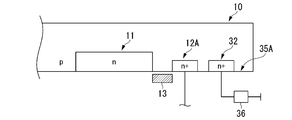
- the reset transistor (resetter) 35A of the modified example shown in FIG. 6 does not have a reset gate 34 and has a voltage signal generation unit 36.
- the depletion layer around the drain 32 is connected to the depletion layer of the first charge storage unit 12A, and the potential of the first charge storage unit 12A is coupled and depleted. It can be set to a characteristic voltage determined by the potential distribution of the layer. That is, the first charge storage unit 12A can be reset. As a result, the potential of the first charge storage unit can be reset without using an FET gate such as the reset gate 34.
- each first charge storage unit and the drain 32 it is possible to make a difference in the impurity concentrations of each first charge storage unit and the drain 32. It is also possible to form an appropriate impurity region between each first charge storage unit and the drain 32 for the same purpose.
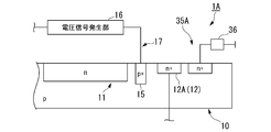
- FIG. 7 is a diagram in which a reset transistor 35A is provided on the solid-state image sensor 1A.
- the solid-state image sensor 1A has a transfer controller 17 and performs distribution driving by an externally applied voltage. Therefore, when the reset transistor 35A is provided, the FET gate does not exist in the first semiconductor 10. As a result, the manufacturing process can be greatly simplified and the manufacturing cost can be significantly reduced.
- FIG. 8 is an example in which a drain structure 38 for eliminating signal charges (electrons when the first semiconductor 10 is P-type) is added to the first semiconductor 10.
- the drain structure 38 has a voltage signal generation unit 39.
- a voltage that is in a reverse bias state with that of the first semiconductor 10 is applied from the voltage signal generation unit 39 to the drain structure 38, unnecessary charges of the first charge storage unit 12A are discharged to the drain structure 38.
- unnecessary charges can be eliminated in advance and the S / N ratio of the distribution signal is improved.
- FIG. 9 is a diagram in which a drain structure 38 is added to the solid-state image sensor 1A. Also in this case, it is not necessary to form the FET gate in the first semiconductor 10. In both FIGS. 8 and 9, the drain structure 38 is combined with the reset transistor 35A. In this case, the drain structure 38 and the reset transistor 35A may share a part of the structure.
- a charge discharging unit 18 connected to the photodiode 11 via a gate may be provided in the first semiconductor 10.
- the electric charges generated by the incident light generated in the photodiode 11 and the electric charges generated by the dark current can be suitably discharged.
- one part of the first charge storage part 12B and each part of the associated second semiconductor 30 are omitted.
- the transfer gate 13 of the solid-state image sensor 1B is replaced with a transfer controller 17 having a p + type semiconductor region 15 and a voltage signal generation unit 16, and the gate of the charge discharge unit 18 is replaced with a p + type semiconductor region 18a and a voltage signal generation unit.
- the first semiconductor 10 has a configuration in which the FET gate does not exist, and the above-mentioned advantages can be obtained.
- the charge discharge unit 18 may be combined with a reset transistor or a drain structure.
Landscapes
- Engineering & Computer Science (AREA)
- Multimedia (AREA)
- Signal Processing (AREA)
- Solid State Image Pick-Up Elements (AREA)
- Transforming Light Signals Into Electric Signals (AREA)
Abstract
固体撮像素子は、第一半導体と、第一半導体と異なる組成を有し、第一半導体と電気的に接続された第二半導体とを備える。第一半導体は、入射光により光電変換を行うフォトダイオードと、光電変換により発生した電荷を蓄積する複数の第一電荷蓄積部と、光電変換により発生した電荷を複数の第一電荷蓄積部のいずれかに移動させる転送ゲートとを有する。第二半導体は電荷を蓄積することのできる第二電荷蓄積部と、第二電荷蓄積部の電位を検出する電位検出ノードとを有する。固体撮像素子は、さらに、第一電荷蓄積部の電位を所定の電位にリセットするリセットトランジスタを備える。
Description
本発明は、固体撮像素子、および撮像システムに関する。
本願は、2020年3月25日に日本に出願された特願2020-054149号に基づき優先権を主張し、その内容をここに援用する。
本願は、2020年3月25日に日本に出願された特願2020-054149号に基づき優先権を主張し、その内容をここに援用する。
撮像素子は、様々な分野で利用されている。その一つに、測距可能な撮像システムがある。
このような撮像システムは、一般に被写体に照射する光を生成する光源と、撮像素子とを備える。撮像素子は、被写体からの反射光を撮像する撮像センサとして機能する。
このような撮像システムは、一般に被写体に照射する光を生成する光源と、撮像素子とを備える。撮像素子は、被写体からの反射光を撮像する撮像センサとして機能する。
上記撮像素子に関する課題として、外光に起因するノイズがある。このノイズを低減する対策の一つとして、太陽光にほとんど含まれない近赤外から短波長赤外の波長帯域(好ましくは、太陽光にほとんど含まれない1350nm~1400nm程度)の光を使用することが検討されている。これにより、太陽光を含む多くの外光の影響をほぼゼロにできる。
このような波長帯域の光を使用して測距可能な撮像システムを構築するためには、当該波長帯域の光を効率よく光電変換できる撮像素子が必要であり、高い吸収係数を有するゲルマニウム(Ge)などを用いて構成することが考えられている。
特許文献1には、Geおよびケイ素(Si)を含有する層にフォトダイオードを形成したデバイスが開示されている。
特許文献1には、Geおよびケイ素(Si)を含有する層にフォトダイオードを形成したデバイスが開示されている。
特許文献1に記載のデバイスは、フォトダイオードが形成された第一の半導体と、シリコン基板に形成された第二の半導体とを有する。第一の半導体で光電変換により発生した電荷は第二の半導体に移動されて電荷電圧変換が行われるが、電荷が具体的にどのように転送されるかについては説明がなく、導電体配線と拡散層とを用いた公知のインターコネクションが例示されているのみである。
撮像素子において、フォトダイオードで発生した電荷が、複数の電荷蓄積領域に振り分け駆動されることがある。特許文献1にも、第二の半導体に転送された電荷が二つの電荷蓄積領域に振り分け駆動されるTOF(time of flight)方式の光センサが記載されている。
しかし、特許文献1に記載のデバイスにおいて第一の半導体と第二の半導体とが例示された上述の態様で接合されている場合、フォトダイオードと振り分けを行うゲートとの間に拡散層が存在するため、実際には振り分け駆動が好適に行われない可能性がある。
しかし、特許文献1に記載のデバイスにおいて第一の半導体と第二の半導体とが例示された上述の態様で接合されている場合、フォトダイオードと振り分けを行うゲートとの間に拡散層が存在するため、実際には振り分け駆動が好適に行われない可能性がある。
上記事情を踏まえ、本発明は、近赤外から短波長赤外の波長帯域の光を効率よく利用でき、かつ振り分け駆動が良好に行える固体撮像素子を提供することを目的とする。
本発明の第一の態様に係る固体撮像素子は、第一半導体と、第一半導体と異なる組成を有し、第一半導体と電気的に接続された第二半導体とを備える。
第一半導体は、入射光により光電変換を行うフォトダイオードと、光電変換により発生した電荷を蓄積する複数の第一電荷蓄積部と、光電変換により発生した電荷を第一電荷蓄積部のいずれかに移動させる転送コントローラーとを有する。
第二半導体は、電荷を蓄積することのできる第二電荷蓄積部と、第二電荷蓄積部の電位を検出する電位ディテクターとを有する。
固体撮像素子は、さらに、第一電荷蓄積部の電位を所定の電位にリセットするリセッターを備えている。
第一半導体は、入射光により光電変換を行うフォトダイオードと、光電変換により発生した電荷を蓄積する複数の第一電荷蓄積部と、光電変換により発生した電荷を第一電荷蓄積部のいずれかに移動させる転送コントローラーとを有する。
第二半導体は、電荷を蓄積することのできる第二電荷蓄積部と、第二電荷蓄積部の電位を検出する電位ディテクターとを有する。
固体撮像素子は、さらに、第一電荷蓄積部の電位を所定の電位にリセットするリセッターを備えている。
本発明の第二の態様に係る撮像システムは、所定の波長プロファイルを有する出射光を出射する光源部と、第一の態様に係る固体撮像素子とを備える。
本発明の上記態様によれば、近赤外から短波長赤外の波長帯域の光を効率よく利用でき、振り分け駆動が良好に行える。
本発明の一実施形態について、図1から図4を参照して説明する。
図1は、本実施形態に係る固体撮像素子1の構成を示す模式図である。固体撮像素子1は、第一半導体10と、第二半導体30とが電気的に接続されて構成されている。第一半導体10と第二半導体30とは、構成元素の組成が異なっており、互いに異なる格子定数を有する。
図1は、本実施形態に係る固体撮像素子1の構成を示す模式図である。固体撮像素子1は、第一半導体10と、第二半導体30とが電気的に接続されて構成されている。第一半導体10と第二半導体30とは、構成元素の組成が異なっており、互いに異なる格子定数を有する。
第一半導体10は、公知のフォトダイオード(PD、Photodiode)11を有し、入射した光を光電変換し、信号電荷を蓄積可能に構成されている。フォトダイオード11は、第一半導体10の不純物濃度等により省略することも可能である。この場合は第一半導体10においてフォトダイオード11が占めている幾何学的な領域が光電変換の機能を持つ。
第一半導体10は、少なくともフォトダイオード11の部分において、近赤外から短波長赤外の波長帯域、特に1350nm~1400nm程度の波長帯域の光の吸収特性に優れた元素あるいは化合物を多く含んで構成されている。このような物質としては、Geが典型的であり、他にGeSi(ゲルマニウムシリコン)等のゲルマニウム化合物やGaSb(アンチモン化ガリウム)等を例示できる。以下、これらの物質を総称して、「Ge等」と称することがある。
第一半導体10の物理的構造には特に制限はなく、全体がGe単独またはGe等の混晶で形成された一様の組成であってもよいし、Ge等がシリコン等の他の物質と交互に積層された構成を有してもよい。
第一半導体10は、少なくともフォトダイオード11の部分において、近赤外から短波長赤外の波長帯域、特に1350nm~1400nm程度の波長帯域の光の吸収特性に優れた元素あるいは化合物を多く含んで構成されている。このような物質としては、Geが典型的であり、他にGeSi(ゲルマニウムシリコン)等のゲルマニウム化合物やGaSb(アンチモン化ガリウム)等を例示できる。以下、これらの物質を総称して、「Ge等」と称することがある。
第一半導体10の物理的構造には特に制限はなく、全体がGe単独またはGe等の混晶で形成された一様の組成であってもよいし、Ge等がシリコン等の他の物質と交互に積層された構成を有してもよい。
以下、第一半導体10がP型であることを前提として説明を行うが、第一半導体10がN型である場合も同様な説明が可能である。また、半導体がP型である場合には、図中に「p」を付す場合がある。同様に、N型である場合には「n」を、p+型半導体領域である場合には「p+」を、n+型半導体領域である場合には「n+」を、付す場合がある。
第一半導体10は、複数の第一電荷蓄積部12を有する。本実施形態の第一電荷蓄積部12は、例えばn+型半導体領域である。第一半導体10には、第一電荷蓄積部12Aと第一電荷蓄積部12Bとを含む2つの第一電荷蓄積部12が設けられている。フォトダイオード11と各々の第一電荷蓄積部12との間には、転送ゲート(転送コントローラー)13が設けられている。転送ゲート(転送コントローラー)13は、フォトダイオードの光電変換により発生した電荷を複数の第一電荷蓄積部12のうちのいずれかに移動させる。転送ゲート13の構造は公知であり、例えばMOS(Metal Oxide Semiconductor)構造である。
第一半導体10は、複数の第一電荷蓄積部12を有する。本実施形態の第一電荷蓄積部12は、例えばn+型半導体領域である。第一半導体10には、第一電荷蓄積部12Aと第一電荷蓄積部12Bとを含む2つの第一電荷蓄積部12が設けられている。フォトダイオード11と各々の第一電荷蓄積部12との間には、転送ゲート(転送コントローラー)13が設けられている。転送ゲート(転送コントローラー)13は、フォトダイオードの光電変換により発生した電荷を複数の第一電荷蓄積部12のうちのいずれかに移動させる。転送ゲート13の構造は公知であり、例えばMOS(Metal Oxide Semiconductor)構造である。
第二半導体30は、主に信号処理を行う半導体であり、例えばシリコンで形成されている。第二半導体30は、拡散層を介したインターコネクションにより、第一半導体10と電気的に接続されている。
第二半導体30は、第二電荷蓄積部33と、リセットトランジスタ(リセッター)35のドレイン32と、電位検出ノード31(電位ディテクター)と、リセットトランジスタ(リセッター)35のリセットゲート34とを有する。各第二電荷蓄積部33は、図示しない読み出し回路に接続されている。電位検出ノード31(電位ディテクター)は、第二電荷蓄積部33の電位を検出する。リセットトランジスタ(リセッター)35のリセットゲート34は、第二電荷蓄積部33とドレイン32との間の電荷移動を制御する。
リセットトランジスタ(リセッター)35は、第一電荷蓄積部12の電位を所定の電位にリセットする。リセットトランジスタ35は、例えば、FET(Field Effect Transistor)であってもよい。
第二電荷蓄積部33と、ドレイン32と、電位検出ノード31、およびリセットゲート34は、各第一電荷蓄積部12Aおよび12Bに対応して設けられており、電位検出ノード31は、対応する第二電荷蓄積部33の電位を検出可能に構成されている。
リセットトランジスタ(リセッター)35は、第一電荷蓄積部12の電位を所定の電位にリセットする。リセットトランジスタ35は、例えば、FET(Field Effect Transistor)であってもよい。
第二電荷蓄積部33と、ドレイン32と、電位検出ノード31、およびリセットゲート34は、各第一電荷蓄積部12Aおよび12Bに対応して設けられており、電位検出ノード31は、対応する第二電荷蓄積部33の電位を検出可能に構成されている。
上記のように構成された本実施形態の固体撮像素子1においては、各転送ゲート13に制御信号としての電圧が印加されることにより、フォトダイオード11に生じた電荷が、第一電荷蓄積部12A、12Bのいずれか一方に転送される。制御信号により、電荷の転送先が経時的に変更されることにより、電荷の振り分け駆動が行われる。
固体撮像素子1においては、フォトダイオード11に生じた電荷は第一半導体10内で振り分け駆動された後、拡散層である第一電荷蓄積部12(12A、12B)および対応する第二電荷蓄積部33、ならびに第一電荷蓄積部12と第二電荷蓄積部33とを接続する接続線(不図示)と、第二半導体30内のゲート電極とからなる静電容量に転送される。したがって、静電容量に入った電荷はそれ以降振り分けされない。
一般に、電荷振り分け動作が比較的容量の大きな静電容量で行われるときは特性的な問題が起こりやすい。特に、高速の振り分けが起こる場合は、静電容量からの電荷移動時間が問題となるので、良好な振り分け特性の実現が困難である場合がある。
本実施形態の固体撮像素子1においては、振り分け駆動が第一半導体10内で行われる。そのため、大きな静電容量からの電荷移動という問題が生じない。その結果、振り分け駆動が好適に行われる。
一般に、電荷振り分け動作が比較的容量の大きな静電容量で行われるときは特性的な問題が起こりやすい。特に、高速の振り分けが起こる場合は、静電容量からの電荷移動時間が問題となるので、良好な振り分け特性の実現が困難である場合がある。
本実施形態の固体撮像素子1においては、振り分け駆動が第一半導体10内で行われる。そのため、大きな静電容量からの電荷移動という問題が生じない。その結果、振り分け駆動が好適に行われる。
以上により、本実施形態の固体撮像素子1は、転送コントローラーとしての転送ゲート13と転送先としての第一電荷蓄積部12とを有する第一半導体10を備える。これにより、異質の半導体である第一半導体10および第二半導体30をヘテロ接合した構成でありながら、好適な振り分け駆動を実現できる。
固体撮像素子1では、Ge等を主要物質として第一半導体10のフォトダイオード11が構成されている。これにより、近赤外から短波長赤外の波長帯域、特に1350nm~1400nm程度の波長帯域の光を用いるマルチゲートタイプのTOFセンサとして好適に動作可能な構造であると言える。
固体撮像素子1では、Ge等を主要物質として第一半導体10のフォトダイオード11が構成されている。これにより、近赤外から短波長赤外の波長帯域、特に1350nm~1400nm程度の波長帯域の光を用いるマルチゲートタイプのTOFセンサとして好適に動作可能な構造であると言える。
本実施形態において、第一電荷蓄積部の数は適宜設定できる。すなわち、上述の例では2つの第一電荷蓄積部を有する例を説明したが、3以上の電荷蓄積部が設けられてもよい。
図2に、本実施形態の変形例に係る固体撮像素子1Aの模式図を示す。固体撮像素子1Aにおいては、転送ゲート13に代えてp+型半導体領域15がフォトダイオード11と第一電荷蓄積部12との間に設けられている。各p+型半導体領域15には、電圧信号発生部16が接続されており、電圧信号発生部16の信号に基づいて、フォトダイオード11に生じた電荷が、第一電荷蓄積部12A、12Bのいずれか一方に転送される。
すなわち、固体撮像素子1Aの転送コントローラー17はp+型半導体領域15および電圧信号発生部16を有し、公知のcurrent assistedの手法により振り分け駆動を行う。
本実施形態の固体撮像素子において、転送コントローラーはゲート電極には限られず、このような構成でも、上述した効果を同様に奏する。
図2では、p+型半導体領域15がフォトダイオード11と第一電荷蓄積部12との間に設けられているが、p+型半導体領域15は第一電荷蓄積部12の近傍に位置していればよく、配置に関して自由度があってもよい。
すなわち、固体撮像素子1Aの転送コントローラー17はp+型半導体領域15および電圧信号発生部16を有し、公知のcurrent assistedの手法により振り分け駆動を行う。
本実施形態の固体撮像素子において、転送コントローラーはゲート電極には限られず、このような構成でも、上述した効果を同様に奏する。
図2では、p+型半導体領域15がフォトダイオード11と第一電荷蓄積部12との間に設けられているが、p+型半導体領域15は第一電荷蓄積部12の近傍に位置していればよく、配置に関して自由度があってもよい。
なお、図2では、第一半導体10において、フォトダイオード11が第二半導体と対向しない側に形成されており、表面照射型(FSI、Front Side Illumination)の固体撮像素子を示している。本明細書に記載されたすべての固体撮像素子は、表面照射型および裏面照射型(BSI、Back Side Illumination)のいずれの構成もとることができ、用途や他の構成との関係等に応じて適宜選択できる。
本実施形態に係る固体撮像素子は、単独でも使用できるが、二次元マトリクス状に複数配置されて複数画素を有する撮像素子を構成してもよい。
このような撮像素子の一例を図3にブロック図として示す。撮像素子40は、複数の固体撮像素子1が二次元配列された受光領域41を有する。撮像素子40は、制御回路50、垂直駆動回路60、水平駆動回路70、およびAD変換回路80、および出力回路90を備えているが、これは一例であり、仕様等を考慮して公知の各種構成が適宜組み合わされてもよい。
このような撮像素子の一例を図3にブロック図として示す。撮像素子40は、複数の固体撮像素子1が二次元配列された受光領域41を有する。撮像素子40は、制御回路50、垂直駆動回路60、水平駆動回路70、およびAD変換回路80、および出力回路90を備えているが、これは一例であり、仕様等を考慮して公知の各種構成が適宜組み合わされてもよい。
撮像素子40においては、受光領域41に配置される固体撮像素子の数や配置態様についても、適宜設定できる。複数の固体撮像素子は、隙間なく二次元配列されてもよい。その際、単一の半導体ウエハに二次元配列された複数の固体撮像素子を形成してもよい。
図4に、本実施形態の固体撮像素子を適用した撮像システムの一例を模式的に示す。図4に示す撮像システム100は、光源101を有する光源部110と、撮像センサ121を有する受光部120とを備える。
光源部110は、光源101と、必要に応じて光源101から出る光の波長を整えるフィルタ等を備え、所定の波長および波長帯域(波長プロファイル)を有する出射光L1を被写体Oに向けて出射する。出射光L1は、近赤外から短波長赤外の波長領域の光(例えば、1350nm~1400nm程度の波長帯域)としてもよい。出射光L1が被写体Oに反射されて生じた反射光L2は、受光部120の撮像センサ121に入射する。撮像センサ121としては、本実施形態の固体撮像素子を単独または複数使用できる。
撮像システム100においては、出射光L1の波長プロファイルを1350nm~1400nm程度の波長帯域とすることにより、屋外で使用しても外光の影響をほとんど受けずにTOF法による測距等を好適に行うことができる。
光源部110は、光源101と、必要に応じて光源101から出る光の波長を整えるフィルタ等を備え、所定の波長および波長帯域(波長プロファイル)を有する出射光L1を被写体Oに向けて出射する。出射光L1は、近赤外から短波長赤外の波長領域の光(例えば、1350nm~1400nm程度の波長帯域)としてもよい。出射光L1が被写体Oに反射されて生じた反射光L2は、受光部120の撮像センサ121に入射する。撮像センサ121としては、本実施形態の固体撮像素子を単独または複数使用できる。
撮像システム100においては、出射光L1の波長プロファイルを1350nm~1400nm程度の波長帯域とすることにより、屋外で使用しても外光の影響をほとんど受けずにTOF法による測距等を好適に行うことができる。
以上、本発明の一実施形態について図面を参照して詳述したが、具体的な構成はこの実施形態に限られるものではなく、本発明の要旨を逸脱しない範囲の構成の変更、組み合わせなども含まれる。
例えば、図5に示す変形例の様に、リセットトランジスタ35のドレイン32およびリセットゲート34が第一半導体10に設けられてもよい。この場合、第二半導体30とは単に高抵抗のゲート電極を介して容量結合しているだけであるため、振り分けられた電荷は第一半導体10内のみを移動することになる。その結果、リセット電圧等の設定の自由度が大きく、また拡散層である第二電荷蓄積部33を介したノイズの混入もなく、特性の改善が可能である。
リセットトランジスタの構成は、図5に示す例に限られない。
図6に示す変形例のリセットトランジスタ(リセッター)35Aは、リセットゲート34を有さず、電圧信号発生部36を有している。電圧信号発生部36の信号により、ドレイン32の印加電圧が上昇すると、ドレイン32周辺の空乏層が第一電荷蓄積部12Aの空乏層とつながって、第一電荷蓄積部12Aの電位を、結合空乏層の電位分布で決まる特性的な電圧に設定できる。すなわち、第一電荷蓄積部12Aをリセットできる。これにより、リセットゲート34のようなFETゲートを用いることなく第一電荷蓄積部の電位をリセットできる。なお、リセット動作を制御性良く行うために、各第一電荷蓄積部とドレイン32の不純物濃度に差異をもたせることも可能である。また、同じ目的で各第一電荷蓄積部とドレイン32との間に適当な不純物領域を形成することも可能である。
図6に示す変形例のリセットトランジスタ(リセッター)35Aは、リセットゲート34を有さず、電圧信号発生部36を有している。電圧信号発生部36の信号により、ドレイン32の印加電圧が上昇すると、ドレイン32周辺の空乏層が第一電荷蓄積部12Aの空乏層とつながって、第一電荷蓄積部12Aの電位を、結合空乏層の電位分布で決まる特性的な電圧に設定できる。すなわち、第一電荷蓄積部12Aをリセットできる。これにより、リセットゲート34のようなFETゲートを用いることなく第一電荷蓄積部の電位をリセットできる。なお、リセット動作を制御性良く行うために、各第一電荷蓄積部とドレイン32の不純物濃度に差異をもたせることも可能である。また、同じ目的で各第一電荷蓄積部とドレイン32との間に適当な不純物領域を形成することも可能である。
図7は、固体撮像素子1Aにリセットトランジスタ35Aを設けた図である。この場合も、上述と同様の効果を得ることができる。固体撮像素子1Aは転送コントローラー17を有し、外部印加電圧により振り分け駆動を行う。このため、リセットトランジスタ35Aを設けると、第一半導体10にFETゲートが存在しない構成となる。その結果、製造プロセスを大幅に簡素化でき、製造コストを著しく低減できる。
図8は、第一半導体10に信号電荷(第一半導体10がP型の場合は電子)を排除するドレイン構造38を付け加えた例である。ドレイン構造38は、電圧信号発生部39を有する。電圧信号発生部39から第一半導体10と逆バイアス状態となる電圧がドレイン構造38に印加されると、第一電荷蓄積部12Aの不要な電荷がドレイン構造38に排出される。その結果、不要な電荷を予め排除できて振分信号のS/N比が改善される。
図9は、固体撮像素子1Aにドレイン構造38を付け加えた図である。この場合も、第一半導体10にFETゲートを形成する必要がない。
図8および図9のいずれにおいても、ドレイン構造38は、リセットトランジスタ35Aと組み合わせられる。この場合、ドレイン構造38とリセットトランジスタ35Aとで、一部の構造を共用してもよい。
図8および図9のいずれにおいても、ドレイン構造38は、リセットトランジスタ35Aと組み合わせられる。この場合、ドレイン構造38とリセットトランジスタ35Aとで、一部の構造を共用してもよい。
また、図10に示す変形例の固体撮像素子1Bのように、ゲートを介してフォトダイオード11と接続された電荷排出部18が第一半導体10に設けられてもよい。この場合、 第一半導体10にて電荷の振り分け駆動をしていない期間において、フォトダイオード11に生じた入射した光によって発生する電荷や暗電流によって発生する電荷を好適に排出できる。なお、図10においては、同一面に示すことが難しいため、一方の第一電荷蓄積部12Bおよび対応付けられた第二半導体30の各部を省略している。
図11は、固体撮像素子1Bの転送ゲート13を、p+型半導体領域15および電圧信号発生部16を有する転送コントローラー17に置き換え、電荷排出部18のゲートをp+型半導体領域18aおよび電圧信号発生部18bに置き換えた例である。この場合も、第一半導体10にFETゲートが存在しない構成となり、上述の利点が得られる。
電荷排出部18は、リセットトランジスタやドレイン構造と組み合わされてもよい。
電荷排出部18は、リセットトランジスタやドレイン構造と組み合わされてもよい。
1、1A、1B 固体撮像素子
10 第一半導体
11 フォトダイオード
12、12A、12B 第一電荷蓄積部
13 転送ゲート(転送コントローラー)
17 転送コントローラー
30 第二半導体
31 電位検出ノード(電位ディテクター)
33 第二電荷蓄積部
35、35A リセットトランジスタ(リセッター)
40 撮像素子
100 撮像システム
110 光源部
L1 出射光
10 第一半導体
11 フォトダイオード
12、12A、12B 第一電荷蓄積部
13 転送ゲート(転送コントローラー)
17 転送コントローラー
30 第二半導体
31 電位検出ノード(電位ディテクター)
33 第二電荷蓄積部
35、35A リセットトランジスタ(リセッター)
40 撮像素子
100 撮像システム
110 光源部
L1 出射光
Claims (5)
- 第一半導体と、
前記第一半導体と異なる組成を有し、前記第一半導体と電気的に接続された第二半導体と、
を備え、
前記第一半導体は、
入射光により光電変換を行うフォトダイオードと、
前記光電変換により発生した電荷を蓄積する複数の第一電荷蓄積部と、
前記光電変換により発生した電荷を前記第一電荷蓄積部のいずれかに移動させる転送コントローラーと、を有し、
前記第二半導体は
電荷を蓄積することのできる第二電荷蓄積部と、
前記第二電荷蓄積部の電位を検出する電位ディテクターと、を有し、
前記第一電荷蓄積部の電位を所定の電位にリセットするリセッターを備える、
固体撮像素子。 - 前記リセッターが前記第一半導体に設けられている、
請求項1に記載の固体撮像素子。 - 前記フォトダイオードを構成する主要元素がゲルマニウムである、
請求項1に記載の固体撮像素子。 - 所定の波長プロファイルを有する出射光を出射する光源部と、
請求項1から3のいずれか一項に記載の固体撮像素子と、
を備える、
撮像システム。 - 前記光源部は、前記出射光として近赤外から短波長赤外の波長領域の光を出射する、
請求項4に記載の撮像システム。
Priority Applications (3)
| Application Number | Priority Date | Filing Date | Title |
|---|---|---|---|
| CN202180020789.5A CN115336255B (zh) | 2020-03-25 | 2021-03-10 | 固体摄像元件以及摄像系统 |
| EP21775284.9A EP4131940B1 (en) | 2020-03-25 | 2021-03-10 | Solid-state image sensor and imaging system |
| US17/935,336 US12568698B2 (en) | 2020-03-25 | 2022-09-26 | Solid-state image sensor and imaging system |
Applications Claiming Priority (2)
| Application Number | Priority Date | Filing Date | Title |
|---|---|---|---|
| JP2020-054149 | 2020-03-25 | ||
| JP2020054149A JP7505221B2 (ja) | 2020-03-25 | 2020-03-25 | 固体撮像素子および撮像システム |
Related Child Applications (1)
| Application Number | Title | Priority Date | Filing Date |
|---|---|---|---|
| US17/935,336 Continuation US12568698B2 (en) | 2020-03-25 | 2022-09-26 | Solid-state image sensor and imaging system |
Publications (1)
| Publication Number | Publication Date |
|---|---|
| WO2021193066A1 true WO2021193066A1 (ja) | 2021-09-30 |
Family
ID=77891459
Family Applications (1)
| Application Number | Title | Priority Date | Filing Date |
|---|---|---|---|
| PCT/JP2021/009537 Ceased WO2021193066A1 (ja) | 2020-03-25 | 2021-03-10 | 固体撮像素子および撮像システム |
Country Status (6)
| Country | Link |
|---|---|
| US (1) | US12568698B2 (ja) |
| EP (1) | EP4131940B1 (ja) |
| JP (1) | JP7505221B2 (ja) |
| CN (1) | CN115336255B (ja) |
| TW (1) | TWI878502B (ja) |
| WO (1) | WO2021193066A1 (ja) |
Families Citing this family (4)
| Publication number | Priority date | Publication date | Assignee | Title |
|---|---|---|---|---|
| WO2024057470A1 (ja) * | 2022-09-15 | 2024-03-21 | ソニーセミコンダクタソリューションズ株式会社 | 光検出装置およびその製造方法、並びに電子機器 |
| US12417615B2 (en) | 2023-05-16 | 2025-09-16 | Bank Of America Corporation | System and method for consolidation of alerts and events using image matching of heatmap descriptions of infrastructure status |
| US12505003B2 (en) | 2023-05-17 | 2025-12-23 | Bank Of America Corporation | System and method for multi image matching for outage prediction, prevention, and mitigation for technology infrastructure using hybrid deep learning |
| US12373271B2 (en) | 2023-05-25 | 2025-07-29 | Bank Of America Corporation | System and method for matching multiple featureless images across a time series for outage prediction and prevention |
Citations (3)
| Publication number | Priority date | Publication date | Assignee | Title |
|---|---|---|---|---|
| US20170040362A1 (en) * | 2015-08-04 | 2017-02-09 | Artilux Corporation | Germanium-silicon light sensing apparatus |
| WO2020017345A1 (ja) * | 2018-07-18 | 2020-01-23 | ソニーセミコンダクタソリューションズ株式会社 | 受光素子および測距モジュール |
| JP2020054149A (ja) | 2018-09-27 | 2020-04-02 | 日本電産株式会社 | モータ |
Family Cites Families (9)
| Publication number | Priority date | Publication date | Assignee | Title |
|---|---|---|---|---|
| JP2004304331A (ja) * | 2003-03-28 | 2004-10-28 | Matsushita Electric Ind Co Ltd | 固体撮像装置 |
| JP2008244021A (ja) * | 2007-03-26 | 2008-10-09 | Matsushita Electric Ind Co Ltd | 固体撮像装置およびそれを用いたカメラ |
| WO2017022218A1 (ja) * | 2015-08-04 | 2017-02-09 | パナソニックIpマネジメント株式会社 | 固体撮像装置 |
| CN113099137A (zh) * | 2015-09-30 | 2021-07-09 | 株式会社尼康 | 拍摄元件 |
| JP6706482B2 (ja) * | 2015-11-05 | 2020-06-10 | ソニーセミコンダクタソリューションズ株式会社 | 固体撮像装置および電子機器 |
| CN112929586B (zh) * | 2015-12-03 | 2024-12-06 | 松下知识产权经营株式会社 | 摄像装置 |
| WO2018191539A1 (en) | 2017-04-13 | 2018-10-18 | Artilux Corporation | Germanium-silicon light sensing apparatus ii |
| US10192911B2 (en) * | 2017-05-09 | 2019-01-29 | Apple Inc. | Hybrid image sensors with improved charge injection efficiency |
| TW202003938A (zh) * | 2018-05-18 | 2020-01-16 | 雁丞有限公司 | 疊紗與夾入織物 |
-
2020
- 2020-03-25 JP JP2020054149A patent/JP7505221B2/ja active Active
-
2021
- 2021-03-10 WO PCT/JP2021/009537 patent/WO2021193066A1/ja not_active Ceased
- 2021-03-10 EP EP21775284.9A patent/EP4131940B1/en active Active
- 2021-03-10 CN CN202180020789.5A patent/CN115336255B/zh active Active
- 2021-03-24 TW TW110110533A patent/TWI878502B/zh active
-
2022
- 2022-09-26 US US17/935,336 patent/US12568698B2/en active Active
Patent Citations (3)
| Publication number | Priority date | Publication date | Assignee | Title |
|---|---|---|---|---|
| US20170040362A1 (en) * | 2015-08-04 | 2017-02-09 | Artilux Corporation | Germanium-silicon light sensing apparatus |
| WO2020017345A1 (ja) * | 2018-07-18 | 2020-01-23 | ソニーセミコンダクタソリューションズ株式会社 | 受光素子および測距モジュール |
| JP2020054149A (ja) | 2018-09-27 | 2020-04-02 | 日本電産株式会社 | モータ |
Non-Patent Citations (1)
| Title |
|---|
| See also references of EP4131940A4 |
Also Published As
| Publication number | Publication date |
|---|---|
| EP4131940A4 (en) | 2023-08-23 |
| TW202141778A (zh) | 2021-11-01 |
| JP2021158418A (ja) | 2021-10-07 |
| US12568698B2 (en) | 2026-03-03 |
| US20230014856A1 (en) | 2023-01-19 |
| TWI878502B (zh) | 2025-04-01 |
| JP7505221B2 (ja) | 2024-06-25 |
| CN115336255A (zh) | 2022-11-11 |
| EP4131940A1 (en) | 2023-02-08 |
| EP4131940B1 (en) | 2026-05-06 |
| CN115336255B (zh) | 2026-04-28 |
Similar Documents
| Publication | Publication Date | Title |
|---|---|---|
| WO2021193066A1 (ja) | 固体撮像素子および撮像システム | |
| JP6108280B2 (ja) | 固体撮像装置 | |
| CN109300924B (zh) | 摄像装置 | |
| EP2752877B1 (en) | Unit pixel and light receiving element for image sensor | |
| CN101488509B (zh) | 传感器、固体摄像器件、摄像装置及其制造方法 | |
| JP2023073519A (ja) | 撮像装置 | |
| CN104377215B (zh) | 摄像元件和摄像装置 | |
| WO2012004923A1 (ja) | 固体撮像装置および固体撮像装置の駆動方法 | |
| JP2009506725A (ja) | 4方向共有のピクセル上に2方向共有の蓄積ゲートを設ける方法及び装置 | |
| Burke et al. | CCD technology | |
| US10735652B2 (en) | Method for controlling imaging device, and imaging device | |
| US20250259952A1 (en) | Semiconductor element, apparatus, and chip | |
| CN106129074A (zh) | 背照式cmos图像传感器 | |
| JP2024015381A (ja) | 撮像装置 | |
| CN111370433A (zh) | 摄像装置以及其制造方法 | |
| CN113016071B (zh) | 摄像装置 | |
| JP2015037155A5 (ja) | ||
| US11647641B2 (en) | Photo-sensitive device and a method for light detection in a photo-sensitive device | |
| CN117242585A (zh) | 光接收元件、x射线成像元件和电子设备 | |
| US20250374690A1 (en) | Image sensor | |
| JP2021082785A (ja) | 固体撮像素子および撮像装置 | |
| KR20130007901A (ko) | 후면 조사형 이미지 센서 | |
| CN115295568A (zh) | 图像传感器及其制作方法 | |
| DURINI | formerly Fraunhofer Institute for Microelectronic Circuits and Systems | |
| Burke et al. | Overview paper-CCD technology |
Legal Events
| Date | Code | Title | Description |
|---|---|---|---|
| 121 | Ep: the epo has been informed by wipo that ep was designated in this application |
Ref document number: 21775284 Country of ref document: EP Kind code of ref document: A1 |
|
| NENP | Non-entry into the national phase |
Ref country code: DE |
|
| ENP | Entry into the national phase |
Ref document number: 2021775284 Country of ref document: EP Effective date: 20221025 |