WO2021193237A1 - 電子放出素子およびその製造方法 - Google Patents
電子放出素子およびその製造方法 Download PDFInfo
- Publication number
- WO2021193237A1 WO2021193237A1 PCT/JP2021/010617 JP2021010617W WO2021193237A1 WO 2021193237 A1 WO2021193237 A1 WO 2021193237A1 JP 2021010617 W JP2021010617 W JP 2021010617W WO 2021193237 A1 WO2021193237 A1 WO 2021193237A1
- Authority
- WO
- WIPO (PCT)
- Prior art keywords
- film
- electron
- electrode
- electron emitting
- emitting element
- Prior art date
- Legal status (The legal status is an assumption and is not a legal conclusion. Google has not performed a legal analysis and makes no representation as to the accuracy of the status listed.)
- Ceased
Links
Images




Classifications
-
- H—ELECTRICITY
- H01—ELECTRIC ELEMENTS
- H01J—ELECTRIC DISCHARGE TUBES OR DISCHARGE LAMPS
- H01J1/00—Details of electrodes, of magnetic control means, of screens, or of the mounting or spacing thereof, common to two or more basic types of discharge tubes or lamps
- H01J1/02—Main electrodes
- H01J1/30—Cold cathodes, e.g. field-emissive cathode
- H01J1/312—Cold cathodes, e.g. field-emissive cathode having an electric field perpendicular to the surface, e.g. tunnel-effect cathodes of metal-insulator-metal [MIM] type
-
- C—CHEMISTRY; METALLURGY
- C23—COATING METALLIC MATERIAL; COATING MATERIAL WITH METALLIC MATERIAL; CHEMICAL SURFACE TREATMENT; DIFFUSION TREATMENT OF METALLIC MATERIAL; COATING BY VACUUM EVAPORATION, BY SPUTTERING, BY ION IMPLANTATION OR BY CHEMICAL VAPOUR DEPOSITION, IN GENERAL; INHIBITING CORROSION OF METALLIC MATERIAL OR INCRUSTATION IN GENERAL
- C23C—COATING METALLIC MATERIAL; COATING MATERIAL WITH METALLIC MATERIAL; SURFACE TREATMENT OF METALLIC MATERIAL BY DIFFUSION INTO THE SURFACE, BY CHEMICAL CONVERSION OR SUBSTITUTION; COATING BY VACUUM EVAPORATION, BY SPUTTERING, BY ION IMPLANTATION OR BY CHEMICAL VAPOUR DEPOSITION, IN GENERAL
- C23C16/00—Chemical coating by decomposition of gaseous compounds, without leaving reaction products of surface material in the coating, i.e. chemical vapour deposition [CVD] processes
- C23C16/22—Chemical coating by decomposition of gaseous compounds, without leaving reaction products of surface material in the coating, i.e. chemical vapour deposition [CVD] processes characterised by the deposition of inorganic material, other than metallic material
- C23C16/30—Deposition of compounds, mixtures or solid solutions, e.g. borides, carbides, nitrides
- C23C16/34—Nitrides
- C23C16/342—Boron nitride
-
- H—ELECTRICITY
- H01—ELECTRIC ELEMENTS
- H01J—ELECTRIC DISCHARGE TUBES OR DISCHARGE LAMPS
- H01J1/00—Details of electrodes, of magnetic control means, of screens, or of the mounting or spacing thereof, common to two or more basic types of discharge tubes or lamps
- H01J1/88—Mounting, supporting, spacing, or insulating of electrodes or of electrode assemblies
- H01J1/90—Insulation between electrodes or supports within the vacuum space
-
- H—ELECTRICITY
- H01—ELECTRIC ELEMENTS
- H01J—ELECTRIC DISCHARGE TUBES OR DISCHARGE LAMPS
- H01J2201/00—Electrodes common to discharge tubes
- H01J2201/02—Arrangements for eliminating deleterious effects
-
- H—ELECTRICITY
- H01—ELECTRIC ELEMENTS
- H01J—ELECTRIC DISCHARGE TUBES OR DISCHARGE LAMPS
- H01J2201/00—Electrodes common to discharge tubes
- H01J2201/30—Cold cathodes
- H01J2201/312—Cold cathodes having an electric field perpendicular to the surface thereof
- H01J2201/3125—Metal-insulator-Metal [MIM] emission type cathodes
-
- H—ELECTRICITY
- H01—ELECTRIC ELEMENTS
- H01J—ELECTRIC DISCHARGE TUBES OR DISCHARGE LAMPS
- H01J2209/00—Apparatus and processes for manufacture of discharge tubes
- H01J2209/01—Generalised techniques
- H01J2209/012—Coating
-
- H—ELECTRICITY
- H01—ELECTRIC ELEMENTS
- H01J—ELECTRIC DISCHARGE TUBES OR DISCHARGE LAMPS
- H01J9/00—Apparatus or processes specially adapted for the manufacture, installation, removal, maintenance of electric discharge tubes, discharge lamps, or parts thereof; Recovery of material from discharge tubes or lamps
- H01J9/02—Manufacture of electrodes or electrode systems
- H01J9/022—Manufacture of electrodes or electrode systems of cold cathodes
- H01J9/027—Manufacture of electrodes or electrode systems of cold cathodes of thin film cathodes
Definitions
- the present invention relates to an electron emitting element for emitting electrons and a method for manufacturing the same.
- cold cathode type electron sources and hot cathode type electron sources are known as electron emitting elements (also referred to as “electron sources”) that emit electrons from atoms to the outside.
- the cold cathode type electron source gives electrons energy to jump out of the cathode by applying a high voltage between the cathode and the anode.
- Technologies related to cold cathode type electron sources are being developed in the fields of, for example, flat display devices, lighting, hydrogen generators, electron microscopes, and the like.
- a thin film electron source having a laminated structure of thin films used for a flat display device or the like is known.
- the thin film electron source has a structure in which an upper electrode, an electron accelerating layer, and a lower electrode are laminated, and emits electrons accelerated in the electron accelerating layer into a vacuum.
- the thin film electron source includes, for example, a MIM (Metal-Insulator-Metal, metal-insulator-metal) type electron source, a MOS (Metal-Oxide-Semiconductor) type electron source, a ballistic surface electron source, and the like.
- the upper electrode is also called a surface electrode or an electron transmission electrode and constitutes an electron emission surface.
- the thin film electron source does not have a needle or filament structure, it is also called a planar electron emitting device.
- the flat electron emitting device is not necessarily limited to a flat plate, but also includes a thin film laminated structure having a curved surface that is not in the shape of a needle or a filament.
- the planar electron emitting element has high stability of emitted electrons, high straightness of emitted electrons, can operate at a low voltage of 10 V or less, can operate stably even in a low vacuum, and can emit electrons. It has features such as surface emission and can be manufactured by an existing semiconductor process.
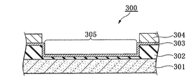
- FIG. 1 is a cross-sectional view schematically showing the configuration of a conventional electron emitting element 300 (see Patent Document 1 and the like).
- the electron emitting element 300 is composed of a lower electrode substrate 301, an insulator layer 302, and an electron transmitting electrode layer 303.
- a noble metal such as gold, platinum, or iridium is used in order to prevent the work function from increasing due to the influence of oxidation or the like.
- the insulator layer 302 has a thickness of a part thereof of 5 nm to 20 nm, functions as an electron acceleration layer, and an electron transmission electrode layer 303 is laminated on the insulator layer 302 to form an electron emission surface.
- the insulator layer 302 in the portion other than the electron emitting surface is thicker than the electron emitting surface and has a thickness of about several tens to several hundreds nm.
- a contact electrode layer 304 for applying a voltage is provided on the portion of the electron transmission electrode layer 303 that does not overlap with the electron emission surface 305.
- the present inventors have proposed an electron emitting element having a laminated structure of graphene / insulating film / silicon using graphene or the like as an electron transmitting electrode as an element for emitting electrons to the outside of a solid (see Patent Document 1).
- the present inventors use an electron source having a structure in which an upper electrode, an electron acceleration layer, and a lower electrode are laminated, and use a graphene film or a graphite film for the upper electrode constituting the electron emitting surface, and the upper electrode and the lower electrode
- an electron source having a curved electron emitting surface in part or in whole (see Patent Document 2).
- the electron emitting element can decompose molecules by emitting electrons in a gas atmosphere or in a liquid and causing electrons to collide with the gas or liquid.
- a hydrogen production apparatus using an electron emitting element has been proposed (see Patent Document 3).
- the present inventors have proposed to provide a protective layer made of a graphene layer or a graphite layer on the surface of a contact electrode layer in an electron emitting element (see Patent Document 3).
- JP-A-2017-45639 Japanese Unexamined Patent Publication No. 2019-71260 Japanese Unexamined Patent Publication No. 2019-21609
- the conventional electron source having a graphene / insulating film / silicon laminated structure can emit electrons not only in a high vacuum but also in a pressure of about low vacuum to atmospheric pressure. ..
- the present inventors have a laminated structure in which a lower electrode made of a semiconductor or a magnetic material, an electron acceleration layer made of an insulating film, and an upper electrode are laminated in this order, and the upper electrode transmits electrons.
- an electron emitting element that is an electrode that emits electrons from the surface and has an energy width of 100 meV or more and 600 meV or less (see Japanese Patent Application No. 2019-88138). This proposal was to realize a narrow energy width of electrons by suppressing the scattering of electrons in the insulating film and the electron transmitting electrode film to the utmost limit.
- graphene having 1 or more layers and 20 or less layers is used as the upper electrode.
- Hexagonal boron nitride is used as the insulating film of the electron acceleration layer.
- the electron transmission electrode when a material that reacts with oxygen, such as graphene, is used as the electron transmission electrode, there arises a problem that the electron emission efficiency is lowered.
- the electron emitting element When the electron emitting element is used in a pressure of about low vacuum to atmospheric pressure, especially when oxygen is present as a residual gas in the gas or low vacuum, the electrons emitted from the electron emitting element Oxygen is excited to generate oxygen radicals.
- the surface of the electron-transmitting electrode is attacked by the oxygen radical, and for example, when the electron-transmitting electrode is graphene, there is a problem that graphene reacts with oxygen and disappears as CO 2. Therefore, even if it is an electron emitting element that can operate in a gas or a low vacuum, it cannot be used unless the oxygen partial pressure is extremely small.
- the electron emitting elements as in Patent Documents 1 to 3 are considered to be used in outer space.
- a propulsion device for an artificial satellite there is a propulsion device called an ion thruster that emits ions into outer space to control the attitude of the artificial satellite.
- the emitted ions often have only a positive charge, so if you continue to emit ions from the ion thruster, the satellite itself will charge up negatively, and the emitted ions will return to the satellite.
- the driving force cannot be obtained. Therefore, in order to maintain the charge balance, it is necessary to emit electrons as well.
- an electron emitting device used for such an application it is desired to efficiently emit electrons at a low voltage.
- the electron emitting element proposed by the present inventors is capable of emitting electrons at a low voltage of about 10 volts and has an extremely high efficiency of 20 to 50%, and is expected as an electron source used for the above-mentioned applications. Has been done.
- the present invention attempts to solve these problems, and the present invention prevents an electron-transmitting electrode from being damaged or chemically changed by being exposed to a gas or a gas in a liquid. It is an object of the present invention to provide an electron emitting element having oxygen resistance and the like, capable of stable operation in an oxygen atmosphere, a gas containing an oxygen atom, and other reactive gases, and having a higher electron emitting efficiency.
- the present invention has the following features in order to achieve the above object.
- the second electrode has a laminated structure in which an electron accelerating layer made of an insulating film, a second electrode, and a coating film are laminated in this order, and the second electrode transmits electrons. It is an electrode that emits electrons from the surface, and the coating film is a film that transmits electrons and is a protective film made of a material different from that of the second electrode, and is characterized by forming an electron emitting surface. An electron emitting element.
- the film thickness of the coating film is characterized in that the reduction rate of the electron emission efficiency by the coating film is within 90% as compared with the case where the coating film is not provided.
- the coating film is one layer or two or more layers selected from MoS 2 , MoSe 2 , WS 2 , WSe 2 , GaS and Gase, and the above (1) to (1).
- the above-mentioned manufacturing method which comprises a step of forming a cover film.
- the coating film is a hexagonal boron nitride film, and in the step of forming the coating film, the hexagonal boron nitride film formed on the substrate is released with the electrons of the electron acceleration layer.
- the coating film is a hexagonal boron nitride film, and in the step of forming the coating film, chemical vapor deposition is carried out using diborane and ammonia, boron trichloride and ammonia, ammonia borane or borazine as raw materials.
- the electron transmitting electrode since a coating film that transmits electrons is further provided on the electron transmitting electrode, the electron transmitting electrode is exposed to a gas such as oxygen in a gas or liquid, an acid / alkali solution, or the like. It is prevented from being damaged or undergoing chemical changes.
- the coating film serves to protect the electron transmitting electrode.
- the characteristics of the high-performance electron emitting device can be maintained. For example, in the present invention, even if electrons are emitted in a gas atmosphere or a liquid to decompose molecules in the medium and oxygen radicals are generated, the surface of the electron permeable electrode is a corrosive gas or liquid such as oxygen.
- the electron emitting element can be operated stably.
- the coating film is hexagonal boron nitride (hereinafter, also referred to as hexagonal boron nitride, h-BN), MoS 2 , MoSe 2 , WS 2 , WSe 2 , GaS, GaSe, SiO 2 ,
- hexagonal boron nitride hereinafter, also referred to as hexagonal boron nitride, h-BN
- MoS 2 , MoSe 2 , WS 2 , WSe 2 , GaS, GaSe, SiO 2 In the case of one layer or two or more layers selected from Al 2 O 3 , ZrO, HfO 2 , and TiO 2, the protective role is remarkable.
- the film thickness can be selectively formed so that the reduction rate of the electron emission efficiency by the coating film is within a predetermined ratio, an element having stable and excellent electron emission efficiency can be obtained according to the environment and application of use. realizable.
- the protective film is hexagonal boron nitride
- the scattering of transmitted electrons is very small compared to other substances, so the electron emission efficiency is not significantly reduced and the electron energy width can be widened. There is no electron emission.
- the surface of the carbon film is coated with a protective film inactive against oxygen or the like by further providing a coating film on the carbon film. Therefore, the carbon surface does not react with oxygen to lose its function as an electrode, or react with oxygen to disappear, and the electron emitting element can be operated stably.
- the present inventor has advanced research and development focusing on the material of the electron emission surface of the thin film laminated structure in the electron emission element, and has come to obtain an electron emission element having improved electron emission efficiency.
- the electron emitting element of the embodiment of the present invention includes a first electrode (also referred to as a "lower electrode”), an electron accelerating layer made of an insulating film, and a second electrode ("upper electrode, surface electrode, electron transmission”. It also has a structure in which an electrode (also referred to as an electrode) and a coating film are laminated in this order.
- the second electrode is an electrode that transmits electrons.
- a coating film that transmits electrons is provided on the surface of the second electrode, and the surface of the coating film on the surface of the second electrode constitutes an electron emission surface.
- the electron emitting surface of the electron emitting device of the present invention is not necessarily limited to a flat plate, but also includes a thin film laminated structure having a curved surface that is not in the shape of a needle or filament.
- the operating principle of the electron emitting element will be described below.
- a positive bias is applied to the upper electrode (or a negative bias is applied to the lower electrode)
- an electric field is generated in the insulating film between the upper electrode and the lower electrode, and the shape of the potential barrier of the insulating film becomes triangular.
- the electric field applied to the insulating film becomes high electric field (10 9 V / m)
- the width of the potential barrier is reduced, the conduction band of the insulating film electron of the lower electrode by quantum mechanical tunneling Tunnel to.
- the electrons tunneled to the conduction band travel in the insulating film due to the high electric field and are emitted through the upper electrode. Therefore, the upper electrode is called an electron transmission electrode.
- the material used for the conventional planar electron emitting element can be used, and the material is not particularly limited.
- SiO 2 , SiN, Al 2 O 3 , h-BN, MgO can be mentioned.
- a silicon oxide film or a boron nitride film is more preferable.
- the film thickness of the insulating film that functions as the electron acceleration layer it is desirable to appropriately select the optimum thickness for the electron acceleration layer.
- a film thickness of about 4 nm or more and 20 nm or less is desirable because the electron emission efficiency is high. If it becomes thinner than 4 nm, electrons will directly tunnel through the insulating film with a bias less than the work function of the electron transmitting electrode. Since the directly tunneled electrons do not have enough energy to overcome the work function of the electron transmitting electrode, they are recovered by the electron transmitting electrode, so that the electron emission efficiency is significantly reduced.
- the electric field applied to the insulating film becomes very high, so that dielectric breakdown is likely to occur and the device life is shortened, which is not preferable.
- it is thicker than 20 nm, the contribution of electron scattering in the insulating film is large, and the energy of most tunnel electrons drops below the work function of the electron transmission electrode and is recovered by the electron transmission electrode. The release efficiency is significantly reduced.
- Hexagonal boron nitride (boron nitride with hexagonal structure, h-BN) thin film is more preferable for applications where it is desired to improve the monochromaticity of energy.
- h-BN has a two-dimensional structure like graphene
- the film thickness can be controlled by controlling the number of layers.
- the scattering of electrons is small, so that h-BN can be expected to significantly improve the electron emission efficiency as compared with the conventional silicon oxide film.
- h-BN electrons with a narrow energy width can be emitted. Narrowing the energy width of emitted electrons is especially important in applications such as electron microscopy.
- SiO 2 is used as the insulating film, about 1 to 1.7 eV can be achieved.
- h-BN is used as the insulating film, a minimum of 0.18 eV can be achieved.
- a metal electrode, a graphene film, a graphite film, or the like As the electron transmission electrode.
- a graphene film or a graphite film a polycrystalline graphene film having one carbon layer or a polycrystalline graphite film having up to about 20 carbon layers is preferable. Further, the graphene film or the graphite film may be nitrogen-doped.
- a metal electrode a metal film composed of one or more selected from Al, Si, Ti, Cr, Fe, Co, Ni, Nb, Mo, Pt, and Au is preferable. It may be a single layer or a plurality of layers.
- the lower electrode is not particularly limited as long as it is a conductive material or a semiconductor material that can be used as an electrode and a material that can realize the laminated structure of the present invention.
- a silicon electrode can be mentioned.
- Silicon is preferably highly conductive, and more preferably N-type in which electrons are present in the conduction band. Silicon may be single crystal, polycrystalline, or amorphous.
- a magnetic metal electrode can be mentioned.
- the coating film is installed for the purpose of protecting the electron emission surface side of the electron transmission electrode from oxygen radicals and the like.
- An oxygen-inert material is used for the coating film.
- a substance having a collision cross section with the electrons as small as possible is desirable. More specifically, it is desirable that the material of the coating film is composed of a light element. Further, in order to be oxygen-inactive, a substance having a structure without dangling bonds (unbonded hands) is desirable. A so-called two-dimensional layered material is desirable.
- a two-dimensional layered material refers to a series of materials having a crystal structure in which the bonds between atoms are closed within the layer and the layers are bonded only by a weak van der Waals force.
- Examples of the two-dimensional layered material include hexagonal boron nitride, MoS 2 , MoSe 2 , WS 2 , WSe 2 , GaS, and GaSe.
- Hexagonal boron nitride is a more desirable material because it is a two-dimensional layered material formed only from boron and nitrogen.
- the coating film constitutes an electron emitting surface, it needs to have electron permeability. As the film thickness of the coating film increases, the electron permeability decreases. Therefore, it is desirable to use an insulating material that can form a film by controlling the film thickness at the atomic level, other than the two-dimensional layered substance. For example, SiO 2 , Al 2 O 3 , ZrO, HfO 2 , TiO 2 and the like can be mentioned.
- the coating film is most preferably h-BN in consideration of electron permeability.
- the film thickness of the coating film is preferably such that the reduction rate of the electron emission efficiency by the coating film is within 90%.
- the electron emitting element 10 includes a lower electrode 1 (first electrode) made of a conductive substrate, a thick insulating film 2 that defines an electron emitting surface 5, and a thin insulating film 6 that functions as an electron accelerating layer of the electron emitting surface 5.
- the electron transmitting electrode 3 surface electrode, upper electrode, second electrode
- the contact electrode 4 also referred to as the third electrode
- the coating film 7 are provided. At least the electron emitting surface region of the surface of the electron transmitting electrode is covered with the coating film 7, and the exposed surface of the coating film 7 constitutes the electron emitting surface.
- the laminated structure of the region constituting the electron emitting surface and the laminated structure of the region not forming the electron emitting surface are almost the same as those of the conventional FIG. 1 except for the presence of the coating film.
- a contact electrode 4 for applying a voltage is provided on a portion of the electron transmission electrode 3 that does not overlap with the electron emission surface 5.
- the material of the contact electrode is not particularly limited. When a voltage of about 5 V to 20 V is applied between the lower electrode 1 and the contact electrode 4, the potential barrier formed in the insulating film 6 becomes thinner, and the electrons in the lower electrode 1 are insulated by the quantum mechanical tunnel effect. Tunneling to the conduction band of the film 6.
- the electrons emitted in the conduction band of the insulating film 6 lose a part of their energy due to the scattering of lattice vibrations, but the electrons having an energy higher than the work function of the electron transmitting electrode 3 pass through the electron transmitting electrode 3 and are further covered. It passes through the cover film 7 and is released into a gas or a liquid such as in a vacuum or the atmosphere.
- the thick insulating film 2 that defines the electron emitting surface 5 and the thin insulating film 6 that functions as the electron accelerating layer of the electron emitting surface 5 may be made of the same material or different materials.
- silicon is used as the lower electrode 1
- a silicon oxide film is simply used as the insulating film.
- a hexagonal boron nitride film is used as the insulating film 6 when it is desired to improve the electron emission efficiency or when it is desired to suppress the electron energy width as much as possible.
- a silicon semiconductor substrate is used as the lower electrode 1.
- the electron transmission electrode 3 is a graphene film having one carbon layer or a graphite film having up to about 20 layers.
- a single-layer graphene film is more preferable.
- the graphite film 7 nm corresponds to about 20 layers. Therefore, the film thickness is more preferably 2 nm or more and 7 nm or less.
- the graphene film or graphite film may be single crystal or polycrystalline.
- a graphene film a polycrystalline film having a crystal grain size of about 50 nm or more and 300 nm or less was used, and good electron emission was obtained.
- it needs to be a continuous film in order to emit electrons from the entire surface.
- the accelerating layer made of an insulating film and graphene or graphite is used for the electron transmitting electrode, it is possible to suppress changes in electron energy distribution due to electron scattering inside the electron emitting element. .. Since the coating film is provided on the electron transmission electrode, the graphene or graphite is not damaged while having the advantage of using graphene or graphite, so that the electron emission efficiency is high and the durability is improved.
- Step 1 Prepare the lower electrode 1.
- a single crystal silicon substrate with a thermal oxide film of 300 nm is prepared (see (a)).
- Step 2 The electron emission surface 5 is defined by using photolithography and etching (see (b)). As an example, the region from which the thermal oxide film 2 has been removed becomes a portion of the electron emission surface.
- Step 3 Clean the substrate in step 2 in order to remove impurities. Cleaning methods used in the field of semiconductors can be used.
- Step 4 A thin insulating film 6 that functions as an electron acceleration layer is formed.
- a silicon oxide film is used as an electron accelerating layer, a method having few defects such as thermal oxidation is preferable (see (c)).
- An electron transmission electrode 3 is formed on the surface of the electron acceleration layer (see (d)).
- An example of the electron transmitting electrode 3 is graphene or graphite.
- the method for forming graphene or graphite is not particularly limited.
- a method suitable for forming an electron transmission electrode there is thermal CVD (thermal chemical vapor deposition) using a metal vapor catalyst and the like.
- the method of forming a graphite film using a metal steam catalyst will be described in detail below.
- polycrystalline graphite having a thickness of 7 nm is uniformly formed on an insulating film (boron nitride film, etc.).
- boron nitride film, etc. boron nitride film, etc.
- a membrane was formed.
- the set temperature, film formation time, gas flow rate ratio, etc. of the electric furnace are not limited to the values disclosed here, and can be appropriately selected according to the required film thickness and crystallinity.
- the gas to be introduced is not limited to argon and methane.
- gallium has been given as an example as a material for a metal steam catalyst, it is not limited to gallium. In addition to gallium, metals such as indium can be used.
- Step 6 A contact electrode 4 for applying a voltage is formed on a portion of the electron transmission electrode 3 that does not overlap with the electron emission surface (see (e)).
- Examples of contact electrodes are Ti / Ni and the like.
- a coating film 7 is formed on the electron transmission electrode 3 (see (f)).
- the coating film 7 constitutes an electron emitting surface.
- An example of a coating film is boron nitride having a hexagonal structure.
- the h-BN film forming method includes a method of transferring a hexagonal boron nitride film formed on another substrate such as Cu or Ni—Fe alloy, ammonia borane (H 6 NB), and borazine (B 3 N). 3 H 6 ), boron trichloride and ammonia, or a CVD method using diborane (B 2 H 6 ) and ammonia (NH 3 ) as raw materials.
- the film forming method is not particularly limited.
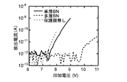
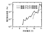
- FIG. 4 shows a comparison of the electron emission characteristics of the electron emitting device with and without the h-BN coating film.
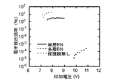
- FIG. 5 shows a comparison of electron emission efficiencies of electron emitting devices with and without an h-BN coating film.
- An electron of the present embodiment including a lower electrode of a silicon semiconductor substrate (n—Si), an insulating film of SiO 2 (example 10 nm), an electron transmission electrode of graphene (example 1 nm), and a coating film of h—BN. The emission element was prepared.
- the h-BN coating film is an electron emitting element having a single layer h-BN (hereinafter, also referred to as “single layer BN”) and an electron emitting element having a multi-layer h-BN (about 39 layers, film thickness 13 nm).
- An element hereinafter, also referred to as “multilayer BN” was prepared.
- Comparative Example 1 an electron emitting element having no coating film was prepared.
- FIGS. 4 and 5 the case of a single-layer BN is shown by a solid line, and the case of a multi-layer BN is shown by a long dotted line.
- FIGS. 4 and 5 the case of the electron emitting element without a coating film (hereinafter, also referred to as “without protective film”) of Comparative Example 1 is shown by a dotted line.
- the electron emission characteristics of the obtained electron beam were evaluated in an ultra-high vacuum chamber.
- the lower electrode cathode
- a voltage is applied to the electron transmission electrode (gate) in 0.1 V steps from 0 V to about + 20 V, and + 1000 V is applied to the SUS plate (anode) that opposes the electron emitting element.
- the lower electrode, the electron transmission electrode, and the current flowing through the SUS plate were measured.
- the electron emission efficiency in the case of single-layer BN, about 10 0% range at an applied voltage of 7V ⁇ 9V. In the case of a multilayer BN, the electron emission efficiency is as low as about 10-4% at an applied voltage of 10 to 11 V. Case without the protective film of Comparative Example 1, the electron emission efficiency at an applied voltage 7V ⁇ 8V is 10 1% or so. In terms of electron emission characteristics, the starting voltage of electron emission tends to be high in the multilayer BN. On the other hand, in the single-layer BN, electron emission can be confirmed from a voltage that is almost the same as that without the protective film. This is because as the number of layers of the BN increases, the electron emission efficiency decreases significantly due to electron scattering in the BN.
- the decrease in electron emission efficiency is about 10% from the case without the protective film, but with the multilayer BN, it is about 98%.
- the protection with the multi-layer BN has a high protective ability of the device because the surface of the device is covered with a thick BN protective layer. It is effective in applications where there is no problem even if the power consumption is high, for example, in applications such as a gas reformer used in a film forming apparatus and charge removal in an analyzer.
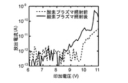
- FIG. 6 to 10 show a comparison of the oxygen-resistant plasma characteristics of the electron emitting device.
- FIG. 6 shows the relationship between the applied voltage and the emission current before and after the irradiation when the electron emitting element without the protective film of Comparative Example 1 is irradiated with oxygen plasma.
- FIG. 7 shows the relationship between the applied voltage and the emission current before and after irradiation in the case of the electron emission element provided with the protective film of the single layer BN of the present embodiment.
- FIG. 8 is an electron emitting element similar to that shown in FIG. 7, and shows the relationship between the applied voltage and the electron emission efficiency before and after irradiation.
- FIG. 6 shows the relationship between the applied voltage and the emission current before and after the irradiation when the electron emitting element without the protective film of Comparative Example 1 is irradiated with oxygen plasma.
- FIG. 7 shows the relationship between the applied voltage and the emission current before and after irradiation in the case of the electron emission element provided with the protective film of the single layer
- FIG. 9 shows the relationship between the applied voltage and the emission current before and after irradiation in the case of the electron emission element provided with the protective film of the multilayer BN.
- FIG. 10 is an electron emitting element similar to that shown in FIG. 9, and shows the relationship between the applied voltage and the electron emission efficiency before and after irradiation.
- Table 1 shows the maximum electron emission efficiency before and after oxygen plasma irradiation in the single-layer h-BN electron emitting element, the multi-layer h-BN electron emitting element, and the comparative example 1 electron emitting element without a protective film. The comparison table of is shown.
- the reason why the electron emission efficiency is increased after the oxygen plasma irradiation is that the organic residue adhering to the h-BN surface, which is a protective film, was burnt down by the oxygen plasma irradiation in the manufacturing process, and the device surface was cleaned. ..
- the film thickness of the coating film can be appropriately set as long as it has a function of transmitting electrons and can play a role of protecting the surface of the electron transmitting electrode. The following will be described with an example of h-BN.
- h-BN When h-BN is used as the coating film, it has been confirmed that electron emission is possible at 13 nm (about 39 layers). Therefore, when h-BN is used, it is preferably 1 layer or more and 39 layers or less.
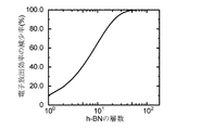
- FIG. 11 is a diagram showing the relationship between the number of layers of h-BN and the reduction rate of electron emission efficiency. From the electron emission efficiency after plasma irradiation with the "without protective film” and "single layer h-BN" protective film in Table 1, the electron transmittance of the single layer h-BN is calculated to be about 90%. From this, the relationship between the number of layers of h-BN and the reduction rate of electron emission efficiency can be derived. Therefore, the number of layers is 21 or less to keep the reduction rate of electron emission efficiency within 90%, and the number of layers is 11 to keep the reduction rate of electron emission efficiency within 70% from the state without the protective film.
- the number of layers is 6 or less to keep the reduction rate of electron emission efficiency within 50%
- the number of layers is 3 or less to keep the reduction rate of electron emission efficiency within 30%
- the reduction rate of electron emission efficiency It is desirable that the number of layers is 2 or less in order to keep the value within 20%.
- the electron emitting surface of the electron emitting element of the present invention is resistant to oxygen and the like, it can be used in a gas atmosphere or a liquid, or in a harsh environment such as outer space. Industrially useful.
Landscapes
- Chemical & Material Sciences (AREA)
- Engineering & Computer Science (AREA)
- Manufacturing & Machinery (AREA)
- Inorganic Chemistry (AREA)
- General Chemical & Material Sciences (AREA)
- Chemical Kinetics & Catalysis (AREA)
- Materials Engineering (AREA)
- Mechanical Engineering (AREA)
- Metallurgy (AREA)
- Organic Chemistry (AREA)
- Cold Cathode And The Manufacture (AREA)
Abstract
本開示では、第1の電極1と、絶縁膜からなる電子加速層6と、第2の電極3と、被覆膜7とが、順に積層されてなる積層構造を備え、上記第2の電極は、電子を透過し、表面から電子を放出する電極であり、上記被覆膜は、電子を透過する膜であり、かつ上記第2電極とは異なる材質の保護膜であり、電子放出面5を構成することを特徴とする、電子放出素子10を提供する。
Description
本発明は、電子を放出するための電子放出素子およびその製造方法に関する。
従来、電子を原子から外部に放出させる電子放出素子(「電子源」とも呼ぶ。)として、冷陰極型電子源と熱陰極型電子源が知られている。冷陰極型電子源は、陰極と陽極間に高電圧を印加することにより、電子に陰極から飛び出すエネルギーを与えるものである。冷陰極型電子源に関する技術は、例えば、平面型ディスプレイ装置、照明、水素発生装置、電子顕微鏡等の分野で開発が進められている。
平面型ディスプレイ装置等に用いる、薄膜の積層構造で構成される薄膜電子源が知られている。薄膜電子源は、上部電極、電子加速層、下部電極を積層した構造を有し、電子加速層中で加速した電子を真空中に放出させる。薄膜電子源には、例えば、MIM(Metal-Insulator-Metal、金属-絶縁体-金属)型電子源、MOS(Metal-Oxide-Semiconductor)型電子源、弾道型面電子源等が含まれる。上部電極は、表面電極又は電子透過電極とも呼ばれ、電子放出面を構成する。薄膜電子源は、針やフィラメント構造ではないので、平面型の電子放出素子とも呼ばれる。平面型の電子放出素子には、必ずしも平板に限らず、針やフィラメント形状ではない曲面を有する薄膜積層構造のものも含む。平面型の電子放出素子は、放出電子の安定性が高いこと、放出電子の直進性が高いこと、10V以下の低電圧で動作可能であること、低真空でも安定動作可能であること、電子を面放出できること、既存の半導体プロセスで作製可能であること等の特徴を有している。
図1は、従来の電子放出素子300の構成を模式的に示す断面図である(特許文献1等参照。)。電子放出素子300は、下部電極基板301、絶縁体層302、および電子透過電極層303より構成される。電子透過電極層303の材料は、酸化などの影響により仕事関数が増加するのを防ぐために、金や白金、イリジウムなどの貴金属が用いられる。絶縁体層302は、その一部分の厚さが5nm~20nmであり、電子加速層として機能し、電子透過電極層303がその上に積層されて電子放出面を構成する。電子放出面以外の部分の絶縁体層302は、電子放出面よりも厚く数十から数百nm程度の厚さである。電子透過電極層303のうち、電子放出面305と重ならない部分の上には、電圧を印加するためのコンタクト電極層304が設けられる。
本発明者らは、固体外部に電子を放出させる素子として、電子透過電極としてグラフェン等を用いた、グラフェン/絶縁膜/シリコンの積層構造を有する電子放出素子を提案した(特許文献1参照)。
本発明者らは、上部電極と電子加速層と下部電極とを積層した構造の電子源であって、電子放出面を構成する上部電極にグラフェン膜又はグラファイト膜を用い、上部電極と下部電極の一部又は全部が曲面を有する、電子放出面が曲面である電子源を提案した(特許文献2参照)。
また、電子放出素子は、ガス雰囲気や液体中において電子放出させ、ガスや液体に電子を衝突させることで分子を分解することが可能である。電子放出素子を用いた水素製造装置が提案されている(特許文献3参照)。例えば、本発明者らは、電子放出素子において、コンタクト電極層の表面にグラフェン層又はグラファイト層からなる保護層を設けることを提案した(特許文献3参照)。
従来の、例えば、特許文献1記載のグラフェン/絶縁膜/シリコン積層構造の電子源は、高真空はもとより、低真空から大気圧程度の圧力中であっても電子を放出することが可能である。例えば、ガスに10eV程度に加速した電子を直接注入し、ガスを分解することが可能となる。また、液体中にガスを注入し同様に液体の分子を分解することが可能となる。
また、本発明者らは、半導体又は磁性体からなる下部電極と、絶縁膜からなる電子加速層と、上部電極とが順に積層されてなる積層構造を備え、上部電極は、電子を透過し、表面から電子を放出する電極であり、放出される電子のエネルギー幅が100meV以上で600meV以下である、電子放出素子を提案している(特願2019-88138参照)。この提案は、絶縁膜中及び電子透過電極膜中の電子の散乱を極限まで抑え、電子の狭エネルギー幅を実現するためであった。この提案では、上部電極として1層以上20層以下のグラフェンを用いている。また、電子加速層の絶縁膜として六方晶系の窒化ホウ素を用いている。
しかしながら、電子透過電極として、グラフェンなどの、酸素と反応する材料を用いた場合、電子放出効率が低下するという問題が生じる。電子放出素子が、低真空から大気圧程度の圧力中で使用されるものであるとき、特に、ガス中や低真空中の残留ガスとして酸素がある場合、電子放出素子から放出された電子によって、酸素が励起されて酸素ラジカルが発生する。その酸素ラジカルにより電子透過電極表面がアタックされて、例えば電子透過電極がグラフェンの場合は、グラフェンが酸素と反応しCO2として消失してしまうという問題がある。そのため、ガス中や低真空中で動作可能な電子放出素子といっても、酸素分圧が極めて小である環境でなければ使用できなかった。
また、酸素雰囲気中だけでなく、CO2等の酸素分子を含むガス中においても、放出された電子によってガスが分解され酸素ラジカルが生成されてしまうという問題がある。そのため、酸素分子を含むガスの分圧が極めて小である環境でなければ使用できなかった。
また、特許文献1~3のような電子放出素子は、宇宙空間での用途が考えられる。人工衛星の推進機として、宇宙空間にイオンを放出して人工衛星の姿勢を制御するイオンスラスターと呼ばれる推進機がある。通常放出されるイオンはプラスの電荷のみを持っていることが多いので、イオンスラスターからイオンを放出し続けると、衛星自体がマイナスにチャージアップして、放出したイオンが衛星に戻ってきてしまい、推進力を得られなくなる問題がある。そこで、チャージバランスを保つために、電子も放出する必要がある。このような用途に使われる電子放出素子としては、低電圧で効率よく電子放出することが望まれる。電子を放出しても推進力には寄与しないので、宇宙空間での限られた電力供給で動作する必要があるため、効率が最も重要な要素である。このように、本発明者らが提案した電子放出素子は、10数ボルトの低電圧で電子放出が可能で、効率が20~50%と非常に高く、上述の用途に使う電子源としても期待されている。
しかし、宇宙空間において使用する、電気推進機の中和銃の場合には、原子状酸素によってグラフェンが消失してしまうという問題がある。これは、宇宙空間には、地表からの高度によるが、例えば地表400kmの高度においては8×10¹³[atoms/m3]程度の濃度の原子状酸素が存在するからである。
本発明は、これらの問題を解決しようとするものであり、本発明は、電子透過電極が、気体や液体中のガスなどに晒されて損傷を受けたり化学変化を受けたりすることを防止し、酸素耐性等を持たせて、酸素雰囲気や、酸素原子を含むガスや、その他反応性のガスにおいて安定に動作でき、電子放出効率がより高い電子放出素子を提供することを目的とする。
本発明は、上記目的を達成するために、以下の特徴を有するものである。
(1) 第1の電極と、絶縁膜からなる電子加速層と、第2の電極と、被覆膜とが、順に積層されてなる積層構造を備え、上記第2の電極は、電子を透過し、表面から電子を放出する電極であり、上記被覆膜は、電子を透過する膜であり、かつ上記第2電極とは異なる材質の保護膜であり、電子放出面を構成することを特徴とする、電子放出素子。
(2) 上記被覆膜は、上記第2の電極より、酸素不活性な膜又は耐腐食性の高い膜であることを特徴とする、上記(1)記載の電子放出素子。
(3) 上記被覆膜の膜厚は、上記被覆膜がない場合と比較して、上記被覆膜による電子放出効率の減少率が90%以内である膜厚であることを特徴とする上記(1)または(2)記載の電子放出素子。
(4) 上記被覆膜は六方晶系の窒化ホウ素であることを特徴とする、上記(1)~(3)のいずれか1項記載の電子放出素子。
(5) 上記被覆膜は1層以上39層以下の六方晶系の窒化ホウ素であることを特徴とする、上記(4)記載の電子放出素子。
(6) 上記第2の電極は、グラフェン膜またはグラファイト膜であることを特徴とする、上記(4)または(5)記載の電子放出素子。
(7) 上記グラフェン膜が炭素1層の多結晶グラフェン膜であり、上記グラファイト膜が炭素20層以下の多結晶グラファイト膜であることを特徴とする、上記(6)記載の電子放出素子。
(8) 上記グラフェン膜および上記グラファイト膜が窒素をドープしてなることを特徴とする、上記(6)または(7)記載の電子放出素子。
(9) 上記電子加速層は、六方晶系の窒化ホウ素であることを特徴とする、上記(4)~(8)のうちいずれか1項記載の電子放出素子。
(10) 上記第2の電極は、金属電極であることを特徴とする、上記(4)または(5)記載の電子放出素子。
(11) 上記被覆膜は、MoS2、MoSe2、WS2、WSe2、GaSおよびGaSeから選択される1層又は2層以上の膜であることを特徴とする、上記(1)~(3)のいずれか1項記載の電子放出素子。
(12) 上記被覆膜は、SiO2、Al2O3、ZrO、HfO2およびTiO2から選択される1層又は2層以上の膜であることを特徴とする、請求項1~3のいずれか1項記載の電子放出素子。
(13) 上記第2の電極は、グラフェン膜またはグラファイト膜であることを特徴とする、上記(11)または(12)記載の電子放出素子。
(14) 上記グラフェン膜が炭素1層の多結晶グラフェン膜であり、上記グラファイト膜が炭素20層以下の多結晶グラファイト膜であることを特徴とする、上記(13)記載の電子放出素子。
(15) 上記グラフェン膜および上記グラファイト膜が窒素をドープしてなることを特徴とする、上記(13)または(14)記載の電子放出素子。
(16) 上記第2の電極は、金属電極であることを特徴とする、上記(11)または(12)記載の電子放出素子。
(17) 電子放出素子の製造方法であって、第1の電極を形成するステップと、上記第1の電極の表面の一部に、電子放出面の領域を規制する第1の絶縁膜を形成するステップと、上記第1の電極および上記第1の絶縁膜を覆う、絶縁膜からなる電子加速層を形成するステップと、上記電子加速層の上記電子放出面の領域に、電子を透過する被覆膜を形成するステップと、を含む、上記製造方法。
(18) 上記被覆膜は、六方晶系の窒化ホウ素膜であり、上記被覆膜を形成するステップにおいて、基板上に形成した六方晶系の窒化ホウ素膜を上記電子加速層の上記電子放出面の領域に転写して上記電子加速層を覆う上記窒化ホウ素膜を形成する、請求項17記載の製造方法。
(19) 上記被覆膜は、六方晶系の窒化ホウ素膜であり、上記被覆膜を形成するステップにおいて、ジボランおよびアンモニア、三塩化ホウ素およびアンモニア、アンモニアボランまたはボラジンを原料として化学気相成長法により上記電子加速層を覆う上記窒化ホウ素膜を形成する、上記(17)記載の製造方法。
(2) 上記被覆膜は、上記第2の電極より、酸素不活性な膜又は耐腐食性の高い膜であることを特徴とする、上記(1)記載の電子放出素子。
(3) 上記被覆膜の膜厚は、上記被覆膜がない場合と比較して、上記被覆膜による電子放出効率の減少率が90%以内である膜厚であることを特徴とする上記(1)または(2)記載の電子放出素子。
(4) 上記被覆膜は六方晶系の窒化ホウ素であることを特徴とする、上記(1)~(3)のいずれか1項記載の電子放出素子。
(5) 上記被覆膜は1層以上39層以下の六方晶系の窒化ホウ素であることを特徴とする、上記(4)記載の電子放出素子。
(6) 上記第2の電極は、グラフェン膜またはグラファイト膜であることを特徴とする、上記(4)または(5)記載の電子放出素子。
(7) 上記グラフェン膜が炭素1層の多結晶グラフェン膜であり、上記グラファイト膜が炭素20層以下の多結晶グラファイト膜であることを特徴とする、上記(6)記載の電子放出素子。
(8) 上記グラフェン膜および上記グラファイト膜が窒素をドープしてなることを特徴とする、上記(6)または(7)記載の電子放出素子。
(9) 上記電子加速層は、六方晶系の窒化ホウ素であることを特徴とする、上記(4)~(8)のうちいずれか1項記載の電子放出素子。
(10) 上記第2の電極は、金属電極であることを特徴とする、上記(4)または(5)記載の電子放出素子。
(11) 上記被覆膜は、MoS2、MoSe2、WS2、WSe2、GaSおよびGaSeから選択される1層又は2層以上の膜であることを特徴とする、上記(1)~(3)のいずれか1項記載の電子放出素子。
(12) 上記被覆膜は、SiO2、Al2O3、ZrO、HfO2およびTiO2から選択される1層又は2層以上の膜であることを特徴とする、請求項1~3のいずれか1項記載の電子放出素子。
(13) 上記第2の電極は、グラフェン膜またはグラファイト膜であることを特徴とする、上記(11)または(12)記載の電子放出素子。
(14) 上記グラフェン膜が炭素1層の多結晶グラフェン膜であり、上記グラファイト膜が炭素20層以下の多結晶グラファイト膜であることを特徴とする、上記(13)記載の電子放出素子。
(15) 上記グラフェン膜および上記グラファイト膜が窒素をドープしてなることを特徴とする、上記(13)または(14)記載の電子放出素子。
(16) 上記第2の電極は、金属電極であることを特徴とする、上記(11)または(12)記載の電子放出素子。
(17) 電子放出素子の製造方法であって、第1の電極を形成するステップと、上記第1の電極の表面の一部に、電子放出面の領域を規制する第1の絶縁膜を形成するステップと、上記第1の電極および上記第1の絶縁膜を覆う、絶縁膜からなる電子加速層を形成するステップと、上記電子加速層の上記電子放出面の領域に、電子を透過する被覆膜を形成するステップと、を含む、上記製造方法。
(18) 上記被覆膜は、六方晶系の窒化ホウ素膜であり、上記被覆膜を形成するステップにおいて、基板上に形成した六方晶系の窒化ホウ素膜を上記電子加速層の上記電子放出面の領域に転写して上記電子加速層を覆う上記窒化ホウ素膜を形成する、請求項17記載の製造方法。
(19) 上記被覆膜は、六方晶系の窒化ホウ素膜であり、上記被覆膜を形成するステップにおいて、ジボランおよびアンモニア、三塩化ホウ素およびアンモニア、アンモニアボランまたはボラジンを原料として化学気相成長法により上記電子加速層を覆う上記窒化ホウ素膜を形成する、上記(17)記載の製造方法。
本発明によれば、電子透過電極の上に、電子を透過する被覆膜をさらに設けるので、電子透過電極が、気体や液体中の、酸素などのガスや、酸・アルカリ溶液などに晒されて、損傷を受けたり化学変化を受けたりすることが防止される。被覆膜は、電子透過電極を保護する役割を果たす。その結果、高性能な電子放出素子の特性を維持できる。例えば、本発明では、ガス雰囲気中や液体中において電子を放出して、その媒質内の分子が分解され、酸素ラジカルが発生したとしても、電子透過電極表面は酸素等の腐食性のガスや液体に対して不活性な保護膜で被覆されているので、電極が酸素等と反応して電極としての機能を果たさなくなる現象が抑制され、酸素と反応して消失したりすることもなくなる。その結果、安定に電子放出素子を動作させることが可能となる。
例えば、被覆膜が、六方晶系の窒化ホウ素(以下、ヘキサゴナル構造のボロンナイトライド、h-BNとも呼ぶ。)、MoS2、MoSe2、WS2、WSe2、GaS、GaSe、SiO2、Al2O3、ZrO、HfO2、TiO2から選択される1層又は2層以上の膜である場合、その保護の役割が顕著である。
被覆膜による電子放出効率の減少率が所定の割合以内であるように、膜厚を選択形成可能であるので、使用する環境や用途に応じて、電子放出効率が安定して優れた素子を実現できる。
保護膜が六方晶窒化ホウ素の場合には、透過する電子の散乱が、他の物質と比べて非常に小さいので、電子放出効率を大きく低下させることもなく、電子のエネルギー幅を広くする事も無く、電子放出可能となる。
本発明において、電子透過電極に、グラフェンやグラファイト等の炭素膜を用いた場合は、炭素膜に被覆膜をさらに設けることにより、炭素膜表面は酸素等に対して不活性な保護膜で被覆されるので、炭素表面が酸素と反応して電極としての機能を果たさなくなったり、酸素と反応して消失したりすることがなく、安定に電子放出素子を動作させることが可能となる。
本発明の実施の形態について以下説明する。
本発明者は、電子放出素子において、薄膜積層構造の電子放出面の材料に着目して研究開発を進め、電子放出効率が向上した電子放出素子を得るに到ったものである。
本発明の実施の形態の電子放出素子は、第1の電極(「下部電極」とも呼ぶ。)と、絶縁膜からなる電子加速層と、第2の電極(「上部電極、表面電極、電子透過電極」とも呼ぶ。)と、被覆膜とが、順に積層された構造を備える。第2の電極は、電子を透過する電極である。第2の電極の表面に、電子を透過する被覆膜が設けられ、第2の電極表面上の被覆膜の表面は、電子放出面を構成する。本発明の電子放出素子における電子放出面は、必ずしも平板に限らず、針やフィラメント形状ではない曲面を有する薄膜積層構造のものも含む。
電子放出素子の動作原理について、以下説明する。上部電極に正のバイアスを印加(または下部電極に負のバイアスを印加)すると、上部電極と下部電極の間の絶縁膜に電界が発生し、絶縁膜の電位障壁の形状が三角形になる。印加するバイアスを高くし、絶縁膜にかかる電界が高電界(109V/m)になると、電位障壁の幅が小さくなり、下部電極の電子が量子力学的トンネル効果によって絶縁膜のコンダクションバンドにトンネルする。コンダクションバンドにトンネルした電子は、高電界により絶縁膜中を走行し、上部電極を貫通して放出される。よって、上部電極は電子透過電極と呼ぶ。上述の先行技術文献などの研究により、電子透過電極にグラフェン又はグラファイトを用いることにより、電子透過電極での電子散乱を抑制することが可能となることが知られている。電子放出効率が最大70%程度まで上げることができると予測される。
電子加速層として機能する絶縁膜として、材料は、従来の平面型の電子放出素子に用いられていた材料を用いることができ、特に制限されない。例えば、SiO2、SiN、Al2O3、h-BN、MgOが挙げられる。シリコン酸化膜や窒化ホウ素膜がより好ましい。
電子加速層として機能する絶縁膜の膜厚は、電子加速層として最適な厚さを適宜選択することが望ましい。4nm以上20nm以下程度の膜厚が、電子放出効率が高くなるので、望ましい。4nmより薄くなってしまうと、電子透過電極の仕事関数以下のバイアスで、絶縁膜を電子がダイレクトトンネルしてしまう。ダイレクトトンネルした電子は電子透過電極の仕事関数を乗り越えるだけのエネルギーを持たないため、電子透過電極で回収されるので、電子放出効率が著しく低下する。また、電子透過電極の仕事関数以上のバイアスを印加した場合、絶縁膜にかかる電界が非常に高くなるため、絶縁破壊が生じやすく素子寿命が短くなるため好ましくない。20nmよりも厚い場合には、絶縁膜での電子散乱の寄与が大きく、大部分のトンネル電子のエネルギーが電子透過電極の仕事関数以下にまで低下し、電子透過電極で回収されてしまうため、電子放出効率が著しく低下する。
エネルギーの単色性を向上させたい用途の場合には、六方晶系の窒化ホウ素(ヘキサゴナル構造のボロンナイトライド、h-BN)薄膜がより好ましい。h-BNは、グラフェンと同様に2次元構造を有しているので、層数を制御することで、膜厚の制御が可能である。また、原子番号が小さいので電子の散乱が小さくなるため、h-BNは、従来のシリコン酸化膜と比べると、電子放出効率の大幅な向上が期待できる。h-BNを用いることにより、エネルギー幅の狭い電子を放出することができる。放出電子のエネルギー幅を狭くすることは、電子顕微鏡などの用途では特に重要である。
絶縁膜を最適化して、絶縁膜での電子散乱を抑制することにより、放出電子のエネルギー幅を0.2eV以下にすることも可能である。絶縁膜にSiO2を用いた場合は1~1.7eV程度を達成できる。絶縁膜にh-BNを用いた場合は、最小0.18eVを達成できる。
電子透過電極として、金属電極、グラフェン膜又はグラファイト膜等を用いることが好ましい。グラフェン膜又はグラファイト膜等の場合は、炭素1層の多結晶グラフェン膜か、炭素20層程度までの多結晶グラファイト膜であることが好ましい。また、グラフェン膜又はグラファイト膜として、窒素をドープしたものであってもよい。金属電極の場合、Al、Si、Ti、Cr、Fe、Co、Ni、Nb、Mo、Pt、Auから選択される1種又は2種以上からなる金属膜が好ましい。単層でも複数層であってもよい。
下部電極は、電極として用いることが可能な導電材料又は半導体材料で、かつ本発明の積層構造を実現可能な材料であれば、特に制限されない。例えば、シリコン電極が挙げられる。シリコンは導電性が高いものが望ましく、伝導帯中に電子が存在するN型がより好ましい。シリコンは、単結晶、多結晶、アモルファス状のいずれでもよい。また、下部電極として、例えば、磁性体金属電極が挙げられる。
被覆膜は、電子透過電極の電子放出表面側を酸素ラジカル等から保護する目的で設置する。被覆膜は、酸素不活性な材料を用いる。さらに、電子の放出効率を下げないためには、透過する電子との相互作用を最小に抑える必要があるので、可能な限り電子との衝突断面積が小さな物質が望ましい。より具体的には、被覆膜の材料は、軽元素からなることが望ましい。また、酸素不活性であるためには、ダングリングボンド(未結合手)がない構造の物質が望ましい。いわゆる二次元層状物質が望ましい。二次元層状物質とは,原子間の結合が層内で閉じていて、層間は弱いファンデルワールス力のみで結合した結晶構造を持つ一連の物質を指す。二次元層状物質として、六方晶系の窒化ホウ素の他、MoS2、MoSe2、WS2、WSe2、GaS、GaSe等が挙げられる。六方晶系の窒化ホウ素は、ホウ素と窒素からのみ形成される二次元層状物質であるので、より望ましい材料である。
被覆膜は、電子放出面を構成するので、電子透過性を有する必要がある。被覆膜の膜厚が増加すると電子透過性が減少するので、二次元層状物質以外でも、原子レベルで膜厚制御をして成膜可能な絶縁材料が望ましい。例えば、SiO2、Al2O3、ZrO、HfO2、TiO2等が挙げられる。被覆膜は、電子透過性を考慮すると、h-BNが最も好ましい。被覆膜の膜厚は、その被覆膜による電子放出効率の減少率が90%以内である膜厚であることが好ましい。
(第1の実施の形態)
本実施の形態について図2を参照して以下説明する。電子放出素子10は、導電性基板からなる下部電極1(第1の電極)と、電子放出面5を規定する厚い絶縁膜2と、電子放出面5の電子加速層として機能する薄い絶縁膜6と、電子透過電極3(表面電極、上部電極、第2の電極)と、コンタクト電極4(第3の電極とも呼ぶ。)と、被覆膜7とを備える。電子透過電極の表面の少なくとも電子放出面領域が被覆膜7により覆われ、被覆膜7の露出面が電子放出面を構成する。
本実施の形態について図2を参照して以下説明する。電子放出素子10は、導電性基板からなる下部電極1(第1の電極)と、電子放出面5を規定する厚い絶縁膜2と、電子放出面5の電子加速層として機能する薄い絶縁膜6と、電子透過電極3(表面電極、上部電極、第2の電極)と、コンタクト電極4(第3の電極とも呼ぶ。)と、被覆膜7とを備える。電子透過電極の表面の少なくとも電子放出面領域が被覆膜7により覆われ、被覆膜7の露出面が電子放出面を構成する。
本実施の形態における、電子放出面を構成する領域の積層構造、及び電子放出面を構成しない領域の積層構造は、被覆膜の存在を除いて、従来の図1とほぼ同じである。電子透過電極3のうち、電子放出面5と重ならない部分の上には、電圧を印加するためのコンタクト電極4が設けられる。コンタクト電極の材料は特に制限されない。下部電極1とコンタクト電極4との間に、5Vから20V程度の電圧を印加すると、絶縁膜6に形成されるポテンシャル障壁が薄くなり、下部電極1中の電子が量子力学的トンネル効果により、絶縁膜6のコンダクションバンドにトンネリングする。絶縁膜6のコンダクションバンドに出た電子は、格子振動の散乱によってエネルギーの一部を失うが、電子透過電極3の仕事関数より高いエネルギーを有する電子は、電子透過電極3を通り抜け、さらに被覆膜7を通り抜けて真空中、大気中等の気体中または液体中に放出される。
電子放出面5を規定する厚い絶縁膜2と、電子放出面5の電子加速層として機能する薄い絶縁膜6とは、同一の材質でも、異なる材質でもよい。下部電極1として、シリコンを用いる場合には、絶縁膜は、シリコン酸化膜が簡便である。電子放出効率を向上したい場合や、電子のエネルギー幅を極力抑えたい様な用途には、絶縁膜6として六方晶窒化ホウ素膜を用いる。
本実施の形態では、下部電極1として、シリコン半導体基板を用いる。
電子透過電極3は、炭素1層のグラフェン膜か、20層程度までのグラファイト膜である。電子透過電極での電子の散乱を極力抑えるためには、単層のグラフェン膜がより好ましい。しかしながら、20層程度までのグラファイト膜であれば、電子放出効率の大幅な劣化は見られないことを確認した。グラファイト膜7nmは、約20層に対応する。よって、2nm以上7nm以下の膜厚であることがより好ましい。グラフェン膜もしくはグラファイト膜は、単結晶でも、多結晶でもよい。例えば、グラフェン膜として、一つの結晶粒の大きさが50nm以上300nm以下程度の多結晶膜を用いて作製して、良好な電子放出が得られた。1層のグラフェンの場合は、全面から電子放出させるために連続膜である必要がある。
例えば、絶縁膜からなる加速層に六方晶系の窒化ホウ素薄膜を用い、電子透過電極にグラフェン又はグラファイトを用いる場合、電子放出素子内部での電子散乱による電子のエネルギー分布変化を抑制することができる。電子透過電極の上に被覆膜を有するので、グラフェン又はグラファイトを用いる利点を有したまま、グラフェンやグラファイトが損傷されることがないので、電子放出効率が高く、耐久性が上がる。
本実施形態の電子放出素子の作製方法について、図3を参照して説明する。
(工程1) 下部電極1を用意する。例として、300nmの熱酸化膜付きの単結晶シリコン基板を用意する((a)参照)。
(工程2) フォトリソグラフィーとエッチングを用いて電子放出面5を規定する((b)参照)。例として、熱酸化膜2が除去された領域が電子放出面の部分となる。
(工程3) 不純物を除去するために、工程2の基板を洗浄する。半導体の分野で用いられる洗浄方法を用いることができる。
(工程4) 電子加速層として機能する薄い絶縁膜6を成膜する。例として、シリコン酸化膜を電子加速層として用いる場合には、熱酸化などの欠陥が少ない方法がよい((c)参照)。
(工程5) 電子加速層の表面に、電子透過電極3を成膜する((d)参照)。電子透過電極3の例は、グラフェンもしくはグラファイトである。グラフェンもしくはグラファイトの成膜方法は、特に限定されない。電子透過電極の成膜に好適な方法として、金属蒸気触媒を用いた熱CVD(thermal chemical vapor deposition)等がある。
金属蒸気触媒を用いて、グラファイト膜を成膜する方法を、以下に詳しく説明する。横型電気炉に石英管を挿入した加熱装置を用意する。電気炉の温度は1050℃程度に設定し、石英管の一方からメタンガスとアルゴンガスの混合ガスを導入する。石英管の内部において、金属ガリウムを石英のボート上に設置する。金属ガリウムの風下には、成膜したい表面に絶縁膜を成膜した下部電極を設置する。下部電極上の絶縁膜(窒化ホウ素膜等)の表面に、均一に必要な膜厚のグラフェンを成膜する。例えば1インチの石英管の中で、アルゴンガスの流量100sccm、メタンガスの流量を1sccmとして、30分間成膜した場合、絶縁膜(窒化ホウ素膜等)上に均一に、膜厚7nmの多結晶グラファイト膜が形成された。成膜時間を短くすることで、単層の多結晶グラフェン膜も成膜可能である。なお、電気炉の設定温度や成膜時間、ガスの流量比などは、ここで開示した値に限定されるものではなく、必要な膜厚や結晶性に応じて適宜選択できる。また、導入するガスは、アルゴンとメタンに限らない。キャリアーとなる不活性ガスと、炭素の供給源となるガスとの組み合わせは、任意に選ぶことができる。金属蒸気触媒の材料として、ガリウムを例としてあげたが、ガリウムに限定されない。ガリウムの他に、インジウム等の金属が利用可能である。
(工程6) 電子透過電極3のうち、電子放出面と重ならない部分の上に、電圧を印加するためのコンタクト電極4を形成する((e)参照)。コンタクト電極の例は、Ti/Ni等である。
(工程7) 電子透過電極3上に被覆膜7を成膜する((f)参照)。被覆膜7は電子放出面を構成する。被覆膜の例は、ヘキサゴナル構造の窒化ホウ素である。h-BNの成膜方法には、CuやNi-Fe合金などの他の基板上に成膜されたヘキサゴナル窒化ホウ素膜を転写する方法や、アンモニアボラン(H6NB)、ボラジン(B3N3H6)、三塩化ホウ素とアンモニア、又はジボラン(B2H6)とアンモニア(NH3)を原料としたCVD法などがある。成膜方法は特に限定されない。
h-BNを成膜するCVD法の例を以下説明する。横型電気炉に石英管を挿入した加熱装置を用意する。真空ポンプにより石英管内の圧力を5×10⁻⁴Pa程度まで下げてから、電気炉の温度を1050℃程度に設定する。石英管の一方からボラジン(B3N3H6)蒸気を導入し、石英管内の圧力が30Pa程度になるように調整する。30分間ボラジン蒸気を導入することにより、h-BNを成膜する。
[電子放出素子の特性の測定]
図4に、h-BN被覆膜の有無による電子放出素子の電子放出特性の比較を図示する。図5に、h-BN被覆膜の有無による電子放出素子の電子放出効率の比較を図示する。シリコン半導体基板(n―Si)の下部電極と、SiO2の絶縁膜(例10nm)と、グラフェンの電子透過電極(例1nm)と、h-BNの被覆膜を備える、本実施形態の電子放出素子を準備した。h-BNの被覆膜が、単層h-BNである電子放出素子(以下、「単層BN」とも称する。)と、多層h-BN(約39層、膜厚13nm)である電子放出素子(以下、「多層BN」とも称する。)を準備した。比較例1として、被覆膜を備えない電子放出素子を準備した。図4および図5では、単層BNの場合を実線で示し、多層BNの場合を長い点線で示した。図4および図5では、比較例1の、被覆膜を備えない電子放出素子(以下、「保護膜無し」とも称する。)の場合を点線で示した。
図4に、h-BN被覆膜の有無による電子放出素子の電子放出特性の比較を図示する。図5に、h-BN被覆膜の有無による電子放出素子の電子放出効率の比較を図示する。シリコン半導体基板(n―Si)の下部電極と、SiO2の絶縁膜(例10nm)と、グラフェンの電子透過電極(例1nm)と、h-BNの被覆膜を備える、本実施形態の電子放出素子を準備した。h-BNの被覆膜が、単層h-BNである電子放出素子(以下、「単層BN」とも称する。)と、多層h-BN(約39層、膜厚13nm)である電子放出素子(以下、「多層BN」とも称する。)を準備した。比較例1として、被覆膜を備えない電子放出素子を準備した。図4および図5では、単層BNの場合を実線で示し、多層BNの場合を長い点線で示した。図4および図5では、比較例1の、被覆膜を備えない電子放出素子(以下、「保護膜無し」とも称する。)の場合を点線で示した。
特性測定は、得られる電子ビームの電子放出特性評価を超高真空チャンバー中で行った。まず、下部電極(cathode)を接地、電子透過電極(gate)に0Vから+20V程度まで0.1Vステップで電圧を印加し、電子放出素子と対抗させたSUSプレート(anode)に+1000Vを印加して、下部電極、電子透過電極、SUSプレートに流れる電流を計測した。
図4に示すように、単層BN及び保護膜無しの場合は、およそ印加電圧7.5Vから電子放出を開始し、印加電圧の増加とともに放出電流が増加することを確認した。単層BNの場合は、印加電圧9Vで放出電流密度10-9Aに到達し、十分な放出電流が得られることを確認した。多層BNの場合は、およそ印加電圧9Vから電子放出を開始し、印加電圧11Vで放出電流密度10-11A以上に到達し、放出電流が得られることを確認した。比較例1の保護膜無しの場合は、印加電圧8Vで放出電流密度10-10Aに到達し、放出電流が得られることを確認した。次に、図5に示すように、電子放出効率は、単層BNの場合は、印加電圧7V~9Vで約100%台である。多層BNの場合は、印加電圧10~11Vで電子放出効率は10-4%前後であり低い。比較例1の保護膜無しの場合は、印加電圧7V~8Vで電子放出効率は101%前後である。電子放出特性において、多層BNでは電子放出の開始電圧が高くなる傾向にある。一方で、単層BNでは、保護膜無しとほぼ変わらない電圧から電子放出を確認できる。これは、BNの層数が多くなると、BN内での電子散乱による電子放出効率の低下が顕著になるためである。これは、図5の電子放出効率の電圧依存性からも明らかである。単層BN保護膜では、電子放出効率の減少は保護膜無しから10%程度であるが、多層BNでは98%程度である。しかしながら、多層BNでの保護は、デバイス表面が厚いBN保護層で覆われているため、デバイスの保護能力が高い。消費電力が高くなっても問題ない用途、例えば、成膜装置に使用するガス改質器、分析装置での帯電除去等の用途において、有効である。
図6~図10に、電子放出素子の耐酸素プラズマ特性の比較を図示する。図6は、比較例1の保護膜無しの電子放出素子に対して酸素プラズマを照射した場合の、照射前後の、印加電圧と放出電流の関係である。図7は、本実施形態の単層BNの保護膜を備える電子放出素子の場合の、照射前後の、印加電圧と放出電流の関係である。図8は、図7と同様の電子放出素子で、照射前後の、印加電圧と電子放出効率との関係である。図9は、多層BNの保護膜を備える電子放出素子の場合の、照射前後の、印加電圧と放出電流の関係である。図10は、図9と同様の電子放出素子で、照射前後の、印加電圧と電子放出効率との関係である。表1に、本実施形態の単層h-BNの電子放出素子、多層h-BNの電子放出素子及び比較例1の保護膜無しの電子放出素子における、酸素プラズマ照射前後での最大電子放出効率の比較表を示す。

表1から、比較例1の保護膜無しの場合は、酸素プラズマ照射後により最大電子放出効率が0となっている。これは、酸素プラズマ照射により、電子放出面の電子透過電極表面が損傷を受けて変化等したためである。一方、単層と多層の保護膜を有するものは、酸素プラズマの照射後に、最大電子放出効率が上昇していることが分かる。このことから、多層のh-BNを備える場合も、保護膜無しの場合と比較して、単層の場合と同様に、酸素耐性を有し、酸素の存在する環境での使用に耐えうる効果を有する。酸素プラズマ照射後に電子放出効率が増加している理由は、製造工程で保護膜であるh-BN表面に付着していた有機残渣が酸素プラズマ照射により焼失し、デバイス表面が清浄化されたためである。
被覆膜の膜厚は、電子を透過する機能を有し、かつ電子透過電極表面を保護する役割を果たすことができる範囲で、適宜設定することができる。h-BNの例で以下説明する。
被覆膜としてh-BNを用いる場合は、13nm(約39層)で電子放出が可能であることを確認している。よって、h-BNを用いる場合は、1層以上39層以下であることが好ましい。
図11は、h-BNの層数と電子放出効率の減少率の関係を示す図である。表1の「保護膜なし」と「単層h-BN」保護膜有りのプラズマ照射後の電子放出効率から、単層h-BNの電子透過率を計算すると約90%となる。ここから、h-BNの層数と電子放出効率の減少率の関係を導くことができる。よって、保護膜無しの状態からの、電子放出効率の減少率を90%以内にするには層数は21層以下、電子放出効率の減少率を70%以内にするには層数は11層以下、電子放出効率の減少率を50%以内にするには層数は6層以下、電子放出効率の減少率を30%以内にするには層数は3層以下、電子放出効率の減少率を20%以内にするには層数は2層以下、が望ましい。
なお、上記実施の形態等で示した例は、発明を理解しやすくするために記載したものであり、この形態に限定されるものではない。
本発明の電子放出素子は、その電子放出面が酸素等に耐性を有しているので、ガス雰囲気や液体中での用途や、宇宙空間のような過酷な環境での用途に採用できるので、産業上有用である。
1 下部電極
2 厚い絶縁膜
3 電子透過電極
4 コンタクト電極
5、305 電子放出面
6 絶縁膜
7 被覆膜
10、300 電子放出素子
301 下部電極基板
302 絶縁体層
303 電子透過電極層
304 コンタクト電極層
2 厚い絶縁膜
3 電子透過電極
4 コンタクト電極
5、305 電子放出面
6 絶縁膜
7 被覆膜
10、300 電子放出素子
301 下部電極基板
302 絶縁体層
303 電子透過電極層
304 コンタクト電極層
Claims (19)
- 第1の電極と、絶縁膜からなる電子加速層と、第2の電極と、被覆膜とが、順に積層されてなる積層構造を備え、
前記第2の電極は、電子を透過し、表面から電子を放出する電極であり、
前記被覆膜は、電子を透過する膜であり、かつ前記第2電極とは異なる材質の保護膜であり、電子放出面を構成することを特徴とする、電子放出素子。 - 前記被覆膜は、前記第2の電極より、酸素不活性な膜又は耐腐食性の高い膜であることを特徴とする、請求項1記載の電子放出素子。
- 前記被覆膜の膜厚は、前記被覆膜がない場合と比較して、前記被覆膜による電子放出効率の減少率が90%以内である膜厚であることを特徴とする、請求項1または2記載の電子放出素子。
- 前記被覆膜は、六方晶系の窒化ホウ素であることを特徴とする、請求項1~3のいずれか1項記載の電子放出素子。
- 前記被覆膜は、1層以上39層以下の六方晶系の窒化ホウ素であることを特徴とする、請求項4記載の電子放出素子。
- 前記第2の電極は、グラフェン膜またはグラファイト膜であることを特徴とする、請求項4または5項記載の電子放出素子。
- 前記グラフェン膜が炭素1層の多結晶グラフェン膜であり、前記グラファイト膜が炭素20層以下の多結晶グラファイト膜であることを特徴とする、請求項6項記載の電子放出素子。
- 前記グラフェン膜および前記グラファイト膜が窒素をドープしてなることを特徴とする、請求項6または7記載の電子放出素子。
- 前記電子加速層は、六方晶系の窒化ホウ素であることを特徴とする、請求項4~8のうちいずれか1項記載の電子放出素子。
- 前記第2の電極は、金属電極であることを特徴とする、請求項4または5記載の電子放出素子。
- 前記被覆膜は、MoS2、MoSe2、WS2、WSe2、GaSおよびGaSeから選択される1層又は2層以上の膜であることを特徴とする、請求項1~3のいずれか1項記載の電子放出素子。
- 前記被覆膜は、SiO2、Al2O3、ZrO、HfO2およびTiO2から選択される1層又は2層以上の膜であることを特徴とする、請求項1~3のいずれか1項記載の電子放出素子。
- 前記第2の電極は、グラフェン膜またはグラファイト膜であることを特徴とする、請求項11または12記載の電子放出素子。
- 前記グラフェン膜が炭素1層の多結晶グラフェン膜であり、前記グラファイト膜が炭素20層以下の多結晶グラファイト膜であることを特徴とする、請求項13項記載の電子放出素子。
- 前記グラフェン膜および前記グラファイト膜が窒素をドープしてなることを特徴とする、請求項13または14記載の電子放出素子。
- 前記第2の電極は、金属電極であることを特徴とする、請求項11または12記載の電子放出素子。
- 電子放出素子の製造方法であって、
第1の電極を形成するステップと、
前記第1の電極の表面の一部に、電子放出面の領域を規制する第1の絶縁膜を形成するステップと、
前記第1の電極および前記第1の絶縁膜を覆う、絶縁膜からなる電子加速層を形成するステップと、
前記電子加速層の前記電子放出面の領域に、電子を透過する被覆膜を形成するステップと、を含む、前記製造方法。 - 前記被覆膜は、六方晶系の窒化ホウ素膜であり、
前記被覆膜を形成するステップにおいて、基板上に形成した六方晶系の窒化ホウ素膜を前記電子加速層の前記電子放出面の領域に転写して前記電子加速層を覆う前記窒化ホウ素膜を形成する、請求項17記載の製造方法。 - 前記被覆膜は、六方晶系の窒化ホウ素膜であり、
前記被覆膜を形成するステップにおいて、ジボランおよびアンモニア、三塩化ホウ素およびアンモニア、アンモニアボランまたはボラジンを原料として化学気相成長法により前記電子加速層を覆う前記窒化ホウ素膜を形成する、請求項17記載の製造方法。
Priority Applications (3)
| Application Number | Priority Date | Filing Date | Title |
|---|---|---|---|
| US17/912,659 US11887802B2 (en) | 2020-03-23 | 2021-03-16 | Electron emitting element and method for manufacturing same |
| CN202180022650.4A CN115315773A (zh) | 2020-03-23 | 2021-03-16 | 电子发射元件及其制造方法 |
| EP21775491.0A EP4131319A4 (en) | 2020-03-23 | 2021-03-16 | ELECTRON-EMITTING ELEMENT AND METHOD FOR PRODUCING THE SAME |
Applications Claiming Priority (2)
| Application Number | Priority Date | Filing Date | Title |
|---|---|---|---|
| JP2020-051288 | 2020-03-23 | ||
| JP2020051288A JP7394453B2 (ja) | 2020-03-23 | 2020-03-23 | 電子放出素子およびその製造方法 |
Publications (1)
| Publication Number | Publication Date |
|---|---|
| WO2021193237A1 true WO2021193237A1 (ja) | 2021-09-30 |
Family
ID=77849341
Family Applications (1)
| Application Number | Title | Priority Date | Filing Date |
|---|---|---|---|
| PCT/JP2021/010617 Ceased WO2021193237A1 (ja) | 2020-03-23 | 2021-03-16 | 電子放出素子およびその製造方法 |
Country Status (5)
| Country | Link |
|---|---|
| US (1) | US11887802B2 (ja) |
| EP (1) | EP4131319A4 (ja) |
| JP (1) | JP7394453B2 (ja) |
| CN (1) | CN115315773A (ja) |
| WO (1) | WO2021193237A1 (ja) |
Cited By (4)
| Publication number | Priority date | Publication date | Assignee | Title |
|---|---|---|---|---|
| US20230268225A1 (en) * | 2022-02-18 | 2023-08-24 | Taiwan Semiconductor Manufacturing Co., Ltd. | Semiconductor device and method of forming the same |
| DE102022111959A1 (de) | 2022-05-12 | 2023-11-16 | KETEK GmbH Halbleiter- und Reinraumtechnik | Ionisationsdetektor und Detektionsverfahren |
| DE102023112454A1 (de) | 2022-05-12 | 2023-11-16 | KETEK GmbH Halbleiter- und Reinraumtechnik | Filteranlage und Trennverfahren |
| DE102022005104A1 (de) | 2022-05-12 | 2024-01-04 | KETEK GmbH Halbleiter- und Reinraumtechnik | Ionisationsdetektor und Detektionsverfahren |
Families Citing this family (3)
| Publication number | Priority date | Publication date | Assignee | Title |
|---|---|---|---|---|
| JP7445550B2 (ja) * | 2020-07-15 | 2024-03-07 | シャープ株式会社 | 電子放出素子 |
| KR20250010629A (ko) * | 2022-06-17 | 2025-01-21 | 엘지전자 주식회사 | 전계 방출 소자 및 그를 이용한 엑스레이 발생 장치 |
| TWI901020B (zh) * | 2023-03-02 | 2025-10-11 | 國立研究開發法人產業技術總合研究所 | 電子源 |
Citations (11)
| Publication number | Priority date | Publication date | Assignee | Title |
|---|---|---|---|---|
| WO2000074098A1 (en) * | 1999-05-28 | 2000-12-07 | Hitachi, Ltd. | Thin-film electron source, display and device |
| JP2003187688A (ja) * | 2001-12-13 | 2003-07-04 | Matsushita Electric Works Ltd | 電界放射型電子源およびその製造方法 |
| JP2007264429A (ja) * | 2006-03-29 | 2007-10-11 | Ricoh Co Ltd | 電子放出素子・帯電装置・プロセスカートリッジ・画像形成装置 |
| JP2008519423A (ja) * | 2004-11-08 | 2008-06-05 | バイオメド・ソリューションズ・エルエルシー | 一体化されたサブナノメートルスケール電子ビームシステム |
| JP2011119071A (ja) * | 2009-12-01 | 2011-06-16 | Sharp Corp | 電子放出素子及びその製造方法、並びに、電子放出装置、帯電装置、画像形成装置、電子線硬化装置、自発光デバイス、画像表示装置、送風装置、冷却装置 |
| JP2013037784A (ja) * | 2011-08-03 | 2013-02-21 | Sharp Corp | 電子放出素子およびその製造方法 |
| JP2016136485A (ja) * | 2015-01-23 | 2016-07-28 | シャープ株式会社 | 電子放出素子、及び電子放出装置 |
| JP2017045639A (ja) | 2015-08-27 | 2017-03-02 | 国立大学法人 筑波大学 | グラフェン膜、電子透過電極及び電子放出素子 |
| JP2019071260A (ja) | 2017-10-11 | 2019-05-09 | 国立研究開発法人産業技術総合研究所 | 電子源及び電子線照射装置並びに電子源の製造方法 |
| JP2019088138A (ja) | 2017-11-08 | 2019-06-06 | Ntn株式会社 | 直流給電用限流コイル |
| JP2019216095A (ja) | 2018-06-07 | 2019-12-19 | 国立研究開発法人産業技術総合研究所 | 電子放出素子とその製造方法、水素製造装置、水素製造方法 |
Family Cites Families (5)
| Publication number | Priority date | Publication date | Assignee | Title |
|---|---|---|---|---|
| CN1216394C (zh) | 2001-09-25 | 2005-08-24 | 松下电工株式会社 | 场致发射型电子源 |
| WO2003049132A1 (en) * | 2001-12-06 | 2003-06-12 | Pioneer Corporation | Electron emitting device and method of manufacturing the same and display apparatus using the same |
| WO2006033166A1 (ja) * | 2004-09-24 | 2006-03-30 | Tadahiro Ohmi | 有機el発光素子、その製造方法および表示装置 |
| US7728503B2 (en) | 2006-03-29 | 2010-06-01 | Ricoh Company, Ltd. | Electron emission element, charging device, process cartridge, and image forming apparatus |
| WO2007119524A1 (ja) * | 2006-03-31 | 2007-10-25 | Pioneer Corporation | 電子放出素子及びその製造方法並びに電子放出素子を用いた光電変換素子、撮像装置及びフラットパネルディスプレイ装置 |
-
2020
- 2020-03-23 JP JP2020051288A patent/JP7394453B2/ja active Active
-
2021
- 2021-03-16 EP EP21775491.0A patent/EP4131319A4/en active Pending
- 2021-03-16 CN CN202180022650.4A patent/CN115315773A/zh active Pending
- 2021-03-16 WO PCT/JP2021/010617 patent/WO2021193237A1/ja not_active Ceased
- 2021-03-16 US US17/912,659 patent/US11887802B2/en active Active
Patent Citations (11)
| Publication number | Priority date | Publication date | Assignee | Title |
|---|---|---|---|---|
| WO2000074098A1 (en) * | 1999-05-28 | 2000-12-07 | Hitachi, Ltd. | Thin-film electron source, display and device |
| JP2003187688A (ja) * | 2001-12-13 | 2003-07-04 | Matsushita Electric Works Ltd | 電界放射型電子源およびその製造方法 |
| JP2008519423A (ja) * | 2004-11-08 | 2008-06-05 | バイオメド・ソリューションズ・エルエルシー | 一体化されたサブナノメートルスケール電子ビームシステム |
| JP2007264429A (ja) * | 2006-03-29 | 2007-10-11 | Ricoh Co Ltd | 電子放出素子・帯電装置・プロセスカートリッジ・画像形成装置 |
| JP2011119071A (ja) * | 2009-12-01 | 2011-06-16 | Sharp Corp | 電子放出素子及びその製造方法、並びに、電子放出装置、帯電装置、画像形成装置、電子線硬化装置、自発光デバイス、画像表示装置、送風装置、冷却装置 |
| JP2013037784A (ja) * | 2011-08-03 | 2013-02-21 | Sharp Corp | 電子放出素子およびその製造方法 |
| JP2016136485A (ja) * | 2015-01-23 | 2016-07-28 | シャープ株式会社 | 電子放出素子、及び電子放出装置 |
| JP2017045639A (ja) | 2015-08-27 | 2017-03-02 | 国立大学法人 筑波大学 | グラフェン膜、電子透過電極及び電子放出素子 |
| JP2019071260A (ja) | 2017-10-11 | 2019-05-09 | 国立研究開発法人産業技術総合研究所 | 電子源及び電子線照射装置並びに電子源の製造方法 |
| JP2019088138A (ja) | 2017-11-08 | 2019-06-06 | Ntn株式会社 | 直流給電用限流コイル |
| JP2019216095A (ja) | 2018-06-07 | 2019-12-19 | 国立研究開発法人産業技術総合研究所 | 電子放出素子とその製造方法、水素製造装置、水素製造方法 |
Non-Patent Citations (1)
| Title |
|---|
| See also references of EP4131319A4 |
Cited By (7)
| Publication number | Priority date | Publication date | Assignee | Title |
|---|---|---|---|---|
| US20230268225A1 (en) * | 2022-02-18 | 2023-08-24 | Taiwan Semiconductor Manufacturing Co., Ltd. | Semiconductor device and method of forming the same |
| DE102022111959A1 (de) | 2022-05-12 | 2023-11-16 | KETEK GmbH Halbleiter- und Reinraumtechnik | Ionisationsdetektor und Detektionsverfahren |
| DE102023112454A1 (de) | 2022-05-12 | 2023-11-16 | KETEK GmbH Halbleiter- und Reinraumtechnik | Filteranlage und Trennverfahren |
| DE102022111959B4 (de) | 2022-05-12 | 2023-12-21 | KETEK GmbH Halbleiter- und Reinraumtechnik | Ionisationsdetektor und Detektionsverfahren |
| DE102022005104A1 (de) | 2022-05-12 | 2024-01-04 | KETEK GmbH Halbleiter- und Reinraumtechnik | Ionisationsdetektor und Detektionsverfahren |
| DE102022005104B4 (de) | 2022-05-12 | 2024-12-12 | KETEK GmbH Halbleiter- und Reinraumtechnik | Ionisationsdetektor und Detektionsverfahren |
| US12272512B2 (en) | 2022-05-12 | 2025-04-08 | KETEK GmbH Halbleiter-und Reinraumtechnik | Ionization detector and detection method |
Also Published As
| Publication number | Publication date |
|---|---|
| EP4131319A1 (en) | 2023-02-08 |
| US20230134647A1 (en) | 2023-05-04 |
| CN115315773A (zh) | 2022-11-08 |
| US11887802B2 (en) | 2024-01-30 |
| EP4131319A4 (en) | 2024-07-17 |
| JP7394453B2 (ja) | 2023-12-08 |
| JP2021150246A (ja) | 2021-09-27 |
Similar Documents
| Publication | Publication Date | Title |
|---|---|---|
| JP7394453B2 (ja) | 電子放出素子およびその製造方法 | |
| Sovizi et al. | Plasma processing and treatment of 2D transition metal dichalcogenides: tuning properties and defect engineering | |
| US12051557B2 (en) | Electron emission device and electron microscope | |
| CN108352397B (zh) | 光敏装置和材料 | |
| US8637118B2 (en) | Method of production of graphene | |
| US20140374960A1 (en) | Method for producing a graphene film | |
| US20230114347A1 (en) | Method of forming transition metal dichalcogenide thin film | |
| Stavale et al. | Morphology and luminescence of ZnO films grown on a Au (111) support | |
| WO2016013984A1 (en) | Process for depositing metal or metalloid chalcogenides | |
| WO2012153816A1 (ja) | カーボンナノチューブの製造方法及び製造装置 | |
| Kimura et al. | Field emission characteristics of BN/GaN structure | |
| JP2006278616A (ja) | 薄膜製造装置、薄膜の製造方法、および薄膜積層体 | |
| JP2006306704A (ja) | 炭素膜の製造方法および炭素膜 | |
| Cultrera | Cathodes for photoemission guns | |
| JP2017514985A (ja) | プラズマ電極用の電気的及び化学的に活性な吸着層 | |
| Lee et al. | Catalyst-free synthesis of ZnO nanorods on metal substrates by using thermal chemical vapor deposition | |
| Mutsukawa et al. | Protective Layer Process of Graphene-Oxide-Semiconductor Electron Emission Devices for Low Earth Orbit Applications | |
| Bhogal | A Review of Functionalising Diamond Surfaces for Thermionic Emission Applications | |
| Nazarova | Chemical Vapour Deposition (CVD) of Graphene on Transition Metals and Its Protective Properties | |
| US7759662B2 (en) | Field electron emission element, a method of manufacturing the same and a field electron emission method using such an element as well as an emission/display device employing such a field electron emission element and a method of manufacturing the same | |
| RU2653843C2 (ru) | Способ повышения плотности и стабильности тока матрицы многоострийного автоэмиссионного катода | |
| Shelepin et al. | The ways of silicon carbide usage in field-emission devices: The technological aspect | |
| JP2008044828A (ja) | カーボンナノチューブ形成装置、カーボンナノチューブ形成方法 | |
| Cheng | Cold Cathodes for Applications in Poor Vacuum and Low Pressure Gas Environments: Carbon Nanotubes Versus Zinc Oxide Nanoneedles | |
| JP2022532572A (ja) | 改良反射モードダイノード |
Legal Events
| Date | Code | Title | Description |
|---|---|---|---|
| 121 | Ep: the epo has been informed by wipo that ep was designated in this application |
Ref document number: 21775491 Country of ref document: EP Kind code of ref document: A1 |
|
| NENP | Non-entry into the national phase |
Ref country code: DE |
|
| ENP | Entry into the national phase |
Ref document number: 2021775491 Country of ref document: EP Effective date: 20221024 |