WO2021199522A1 - 光導波路素子とそれを用いた光変調デバイス及び光送信装置 - Google Patents
光導波路素子とそれを用いた光変調デバイス及び光送信装置 Download PDFInfo
- Publication number
- WO2021199522A1 WO2021199522A1 PCT/JP2020/047464 JP2020047464W WO2021199522A1 WO 2021199522 A1 WO2021199522 A1 WO 2021199522A1 JP 2020047464 W JP2020047464 W JP 2020047464W WO 2021199522 A1 WO2021199522 A1 WO 2021199522A1
- Authority
- WO
- WIPO (PCT)
- Prior art keywords
- optical waveguide
- signal electrode
- optical
- substrate
- electrode
- Prior art date
- Legal status (The legal status is an assumption and is not a legal conclusion. Google has not performed a legal analysis and makes no representation as to the accuracy of the status listed.)
- Ceased
Links
Images


Classifications
-
- G—PHYSICS
- G02—OPTICS
- G02F—OPTICAL DEVICES OR ARRANGEMENTS FOR THE CONTROL OF LIGHT BY MODIFICATION OF THE OPTICAL PROPERTIES OF THE MEDIA OF THE ELEMENTS INVOLVED THEREIN; NON-LINEAR OPTICS; FREQUENCY-CHANGING OF LIGHT; OPTICAL LOGIC ELEMENTS; OPTICAL ANALOGUE/DIGITAL CONVERTERS
- G02F1/00—Devices or arrangements for the control of the intensity, colour, phase, polarisation or direction of light arriving from an independent light source, e.g. switching, gating or modulating; Non-linear optics
- G02F1/01—Devices or arrangements for the control of the intensity, colour, phase, polarisation or direction of light arriving from an independent light source, e.g. switching, gating or modulating; Non-linear optics for the control of the intensity, phase, polarisation or colour
- G02F1/03—Devices or arrangements for the control of the intensity, colour, phase, polarisation or direction of light arriving from an independent light source, e.g. switching, gating or modulating; Non-linear optics for the control of the intensity, phase, polarisation or colour based on ceramics or electro-optical crystals, e.g. exhibiting Pockels effect or Kerr effect
- G02F1/035—Devices or arrangements for the control of the intensity, colour, phase, polarisation or direction of light arriving from an independent light source, e.g. switching, gating or modulating; Non-linear optics for the control of the intensity, phase, polarisation or colour based on ceramics or electro-optical crystals, e.g. exhibiting Pockels effect or Kerr effect in an optical waveguide structure
- G02F1/0356—Devices or arrangements for the control of the intensity, colour, phase, polarisation or direction of light arriving from an independent light source, e.g. switching, gating or modulating; Non-linear optics for the control of the intensity, phase, polarisation or colour based on ceramics or electro-optical crystals, e.g. exhibiting Pockels effect or Kerr effect in an optical waveguide structure controlled by a high-frequency electromagnetic wave component in an electric waveguide structure
-
- G—PHYSICS
- G02—OPTICS
- G02F—OPTICAL DEVICES OR ARRANGEMENTS FOR THE CONTROL OF LIGHT BY MODIFICATION OF THE OPTICAL PROPERTIES OF THE MEDIA OF THE ELEMENTS INVOLVED THEREIN; NON-LINEAR OPTICS; FREQUENCY-CHANGING OF LIGHT; OPTICAL LOGIC ELEMENTS; OPTICAL ANALOGUE/DIGITAL CONVERTERS
- G02F1/00—Devices or arrangements for the control of the intensity, colour, phase, polarisation or direction of light arriving from an independent light source, e.g. switching, gating or modulating; Non-linear optics
- G02F1/01—Devices or arrangements for the control of the intensity, colour, phase, polarisation or direction of light arriving from an independent light source, e.g. switching, gating or modulating; Non-linear optics for the control of the intensity, phase, polarisation or colour
- G02F1/03—Devices or arrangements for the control of the intensity, colour, phase, polarisation or direction of light arriving from an independent light source, e.g. switching, gating or modulating; Non-linear optics for the control of the intensity, phase, polarisation or colour based on ceramics or electro-optical crystals, e.g. exhibiting Pockels effect or Kerr effect
- G02F1/0305—Constructional arrangements
- G02F1/0316—Electrodes
-
- G—PHYSICS
- G02—OPTICS
- G02F—OPTICAL DEVICES OR ARRANGEMENTS FOR THE CONTROL OF LIGHT BY MODIFICATION OF THE OPTICAL PROPERTIES OF THE MEDIA OF THE ELEMENTS INVOLVED THEREIN; NON-LINEAR OPTICS; FREQUENCY-CHANGING OF LIGHT; OPTICAL LOGIC ELEMENTS; OPTICAL ANALOGUE/DIGITAL CONVERTERS
- G02F2201/00—Constructional arrangements not provided for in groups G02F1/00 - G02F7/00
- G02F2201/07—Constructional arrangements not provided for in groups G02F1/00 - G02F7/00 buffer layer
-
- G—PHYSICS
- G02—OPTICS
- G02F—OPTICAL DEVICES OR ARRANGEMENTS FOR THE CONTROL OF LIGHT BY MODIFICATION OF THE OPTICAL PROPERTIES OF THE MEDIA OF THE ELEMENTS INVOLVED THEREIN; NON-LINEAR OPTICS; FREQUENCY-CHANGING OF LIGHT; OPTICAL LOGIC ELEMENTS; OPTICAL ANALOGUE/DIGITAL CONVERTERS
- G02F2201/00—Constructional arrangements not provided for in groups G02F1/00 - G02F7/00
- G02F2201/12—Constructional arrangements not provided for in groups G02F1/00 - G02F7/00 electrode
Definitions
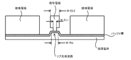
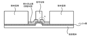
- a rib-structured optical waveguide is provided in a part of the ferroelectric substrate, and a buffer layer such as SiO 2 is further formed.
- the signal electrode may be arranged on the upper side of the rib-structured optical waveguide as shown in FIG.
- a buffer layer is arranged on the upper side of the substrate including the optical waveguide, and the signal electrode and the signal electrode and the signal electrode are further on the upper side of the buffer layer. It is characterized in that a preventive film is arranged.
Landscapes
- Physics & Mathematics (AREA)
- Nonlinear Science (AREA)
- Chemical & Material Sciences (AREA)
- Engineering & Computer Science (AREA)
- Ceramic Engineering (AREA)
- Crystallography & Structural Chemistry (AREA)
- General Physics & Mathematics (AREA)
- Optics & Photonics (AREA)
- Electromagnetism (AREA)
- Optical Modulation, Optical Deflection, Nonlinear Optics, Optical Demodulation, Optical Logic Elements (AREA)
- Optical Integrated Circuits (AREA)
Abstract
Description
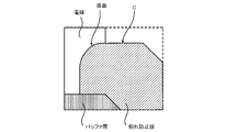
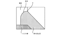
(1) 基板に光導波路を形成し、該光導波路を伝搬する光波を制御するための制御電極を該基板上に配置する光導波路素子において、該制御電極が信号電極を含み、かつ、該信号電極の幅は、基板側の幅が狭い部分と、該信号電極の上部側の幅の広い部分を備え、該信号電極の前記狭い部分に接して配置され、該信号電極が倒れるのを防止する防止膜が該基板上に設けられ、該信号電極の前記狭い部分から前記広い部分に接続する位置では、該防止膜の表面が該信号電極側に突出する曲面で形成され、該曲面に沿うように該信号電極の側面が形成されていることを特徴とする。
本発明の光導波路素子は、図2及び図4乃至6に示すように、基板に光導波路を形成し、該光導波路を伝搬する光波を制御するための制御電極を該基板上に配置する光導波路素子において、該制御電極が信号電極を含み、かつ、該信号電極の幅は、基板側の幅が狭い部分と、該信号電極の上部側の幅の広い部分を備え、該信号電極の前記狭い部分に接して配置され、該信号電極が倒れるのを防止する防止膜が該基板上に設けられ、該信号電極の前記狭い部分から前記広い部分に接続する位置では、該防止膜の表面が該信号電極側に突出する曲面で形成され、該曲面に沿うように該信号電極の側面が形成されていることを特徴とする。
MD 光変調デバイス
OTA 光送信装置
Claims (8)
- 基板に光導波路を形成し、該光導波路を伝搬する光波を制御するための制御電極を該基板上に配置する光導波路素子において、
該制御電極が信号電極を含み、かつ、該信号電極の幅は、基板側の幅が狭い部分と、該信号電極の上部側の幅の広い部分を備え、
該信号電極の前記狭い部分に接して配置され、該信号電極が倒れるのを防止する防止膜が該基板上に設けられ、
該信号電極の前記狭い部分から前記広い部分に接続する位置では、該防止膜の表面が該信号電極側に突出する曲面で形成され、該曲面に沿うように該信号電極の側面が形成されていることを特徴とする光導波路素子。 - 請求項1に記載の光導波路素子において、該防止膜は、永久レジストで構成されていることを特徴とする光導波路素子。
- 請求項1又は2に記載の光導波路素子において、該光導波路は、基板表面に突出したリブ構造の導波路であり、該光導波路の上側に該信号電極が配置されていることを特徴とする光導波路素子。
- 請求項1乃至3のいずれかに記載の光導波路素子において、該基板の厚さは4μm以下であることを特徴とする光導波路素子。
- 請求項1乃至4のいずれかに記載の光導波路素子において、該光導波路を含む該基板の上側にバッファ層が配置され、さらに該バッファ層の上側に該信号電極及び該防止膜が配置されていることを特徴とする光導波路素子。
- 請求項1乃至5のいずれかに記載の光導波路素子と、該光導波路素子を収容する筐体と、該光導波路に光波を該筐体の外部から入力又は出力する光ファイバとを有することを特徴とする光変調デバイス。
- 請求項6に記載の光変調デバイスにおいて、該光導波路素子に入力する変調信号を増幅する電子回路を該筐体の内部に有することを特徴とする光変調デバイス。
- 請求項6又は7に記載の光変調デバイスと、該光変調デバイスに変調動作を行わせる変調信号を出力する電子回路とを有することを特徴とする光送信装置。
Priority Applications (3)
| Application Number | Priority Date | Filing Date | Title |
|---|---|---|---|
| US17/915,716 US12372817B2 (en) | 2020-03-31 | 2020-12-18 | Optical waveguide element, and optical modulation device and optical transmission device using same |
| EP20929211.9A EP4130857A4 (en) | 2020-03-31 | 2020-12-18 | OPTICAL WAVEGUIDE ELEMENT AND OPTICAL MODULATION DEVICE AND OPTICAL TRANSMISSION DEVICE THEREOF |
| CN202080098579.3A CN115335759B (zh) | 2020-03-31 | 2020-12-18 | 光波导元件与使用光波导元件的光调制器件与光发送装置 |
Applications Claiming Priority (2)
| Application Number | Priority Date | Filing Date | Title |
|---|---|---|---|
| JP2020063303A JP7375656B2 (ja) | 2020-03-31 | 2020-03-31 | 光導波路素子とそれを用いた光変調デバイス及び光送信装置 |
| JP2020-063303 | 2020-03-31 |
Publications (1)
| Publication Number | Publication Date |
|---|---|
| WO2021199522A1 true WO2021199522A1 (ja) | 2021-10-07 |
Family
ID=77930193
Family Applications (1)
| Application Number | Title | Priority Date | Filing Date |
|---|---|---|---|
| PCT/JP2020/047464 Ceased WO2021199522A1 (ja) | 2020-03-31 | 2020-12-18 | 光導波路素子とそれを用いた光変調デバイス及び光送信装置 |
Country Status (5)
| Country | Link |
|---|---|
| US (1) | US12372817B2 (ja) |
| EP (1) | EP4130857A4 (ja) |
| JP (1) | JP7375656B2 (ja) |
| CN (1) | CN115335759B (ja) |
| WO (1) | WO2021199522A1 (ja) |
Families Citing this family (3)
| Publication number | Priority date | Publication date | Assignee | Title |
|---|---|---|---|---|
| CN118119879A (zh) * | 2022-09-30 | 2024-05-31 | 住友大阪水泥股份有限公司 | 光波导元件、使用光波导元件的光调制器件及光发送装置 |
| US20250328036A1 (en) * | 2022-09-30 | 2025-10-23 | Sumitomo Osaka Cement Co., Ltd. | Optical Modulator and Optical Transmission Device Using Same |
| CN121311814A (zh) * | 2024-03-28 | 2026-01-09 | 住友大阪水泥株式会社 | 光波导元件及使用其的光调制器以及光发送装置 |
Citations (8)
| Publication number | Priority date | Publication date | Assignee | Title |
|---|---|---|---|---|
| JPH11295675A (ja) * | 1998-04-08 | 1999-10-29 | Nippon Telegr & Teleph Corp <Ntt> | 高速光変調器 |
| US20130170781A1 (en) * | 2011-12-28 | 2013-07-04 | Karl Kissa | Y-branch dual optical phase modulator |
| JP2015061278A (ja) * | 2013-09-20 | 2015-03-30 | 住友電工デバイス・イノベーション株式会社 | 信号伝送路 |
| JP2015216318A (ja) * | 2014-05-13 | 2015-12-03 | 住友電気工業株式会社 | 半導体光集積素子 |
| JP2016161661A (ja) * | 2015-02-27 | 2016-09-05 | 住友大阪セメント株式会社 | 導波路型光素子 |
| US20160291352A1 (en) * | 2015-04-06 | 2016-10-06 | Lumentum Operations Llc | Electrode structures for optical modulators |
| WO2019039215A1 (ja) * | 2017-08-24 | 2019-02-28 | Tdk株式会社 | 光変調器 |
| JP2019045880A (ja) | 2013-11-15 | 2019-03-22 | Tdk株式会社 | 光変調器 |
Family Cites Families (5)
| Publication number | Priority date | Publication date | Assignee | Title |
|---|---|---|---|---|
| JPH11316359A (ja) * | 1998-05-06 | 1999-11-16 | Nippon Telegr & Teleph Corp <Ntt> | 光制御デバイス |
| US20030031400A1 (en) * | 2001-06-28 | 2003-02-13 | Valerio Pruneri | Integrated optical waveguide device |
| JP5897414B2 (ja) * | 2011-08-23 | 2016-03-30 | 日本オクラロ株式会社 | 光デバイスの製造方法 |
| JP6490705B2 (ja) * | 2014-10-06 | 2019-03-27 | 古河電気工業株式会社 | 半導体光集積素子およびその製造方法 |
| JP6290971B2 (ja) * | 2016-04-28 | 2018-03-07 | 住友大阪セメント株式会社 | 光送信装置及び光変調器 |
-
2020
- 2020-03-31 JP JP2020063303A patent/JP7375656B2/ja active Active
- 2020-12-18 US US17/915,716 patent/US12372817B2/en active Active
- 2020-12-18 WO PCT/JP2020/047464 patent/WO2021199522A1/ja not_active Ceased
- 2020-12-18 CN CN202080098579.3A patent/CN115335759B/zh active Active
- 2020-12-18 EP EP20929211.9A patent/EP4130857A4/en active Pending
Patent Citations (8)
| Publication number | Priority date | Publication date | Assignee | Title |
|---|---|---|---|---|
| JPH11295675A (ja) * | 1998-04-08 | 1999-10-29 | Nippon Telegr & Teleph Corp <Ntt> | 高速光変調器 |
| US20130170781A1 (en) * | 2011-12-28 | 2013-07-04 | Karl Kissa | Y-branch dual optical phase modulator |
| JP2015061278A (ja) * | 2013-09-20 | 2015-03-30 | 住友電工デバイス・イノベーション株式会社 | 信号伝送路 |
| JP2019045880A (ja) | 2013-11-15 | 2019-03-22 | Tdk株式会社 | 光変調器 |
| JP2015216318A (ja) * | 2014-05-13 | 2015-12-03 | 住友電気工業株式会社 | 半導体光集積素子 |
| JP2016161661A (ja) * | 2015-02-27 | 2016-09-05 | 住友大阪セメント株式会社 | 導波路型光素子 |
| US20160291352A1 (en) * | 2015-04-06 | 2016-10-06 | Lumentum Operations Llc | Electrode structures for optical modulators |
| WO2019039215A1 (ja) * | 2017-08-24 | 2019-02-28 | Tdk株式会社 | 光変調器 |
Non-Patent Citations (1)
| Title |
|---|
| See also references of EP4130857A4 |
Also Published As
| Publication number | Publication date |
|---|---|
| US12372817B2 (en) | 2025-07-29 |
| CN115335759A (zh) | 2022-11-11 |
| JP2021162681A (ja) | 2021-10-11 |
| EP4130857A1 (en) | 2023-02-08 |
| US20230221590A1 (en) | 2023-07-13 |
| CN115335759B (zh) | 2025-02-25 |
| JP7375656B2 (ja) | 2023-11-08 |
| EP4130857A4 (en) | 2024-05-01 |
Similar Documents
| Publication | Publication Date | Title |
|---|---|---|
| US7925123B2 (en) | Optical control device | |
| US7912326B2 (en) | Optical control device | |
| US8644647B2 (en) | Optical control device | |
| US7035485B2 (en) | Optical waveguide device, and a travelling wave form optical modulator | |
| US8600197B2 (en) | Optical control device | |
| US8396334B2 (en) | Optical waveguide device | |
| WO2021199522A1 (ja) | 光導波路素子とそれを用いた光変調デバイス及び光送信装置 | |
| JP2008089936A (ja) | 光制御素子 | |
| CN113646690B (zh) | 光调制器 | |
| CN115280227B (zh) | 光波导元件、使用该光波导元件的光调制器件及光发送装置 | |
| WO2022163724A1 (ja) | 光変調器とそれを用いた光送信装置 | |
| JP2020060742A (ja) | 光導波路素子および光変調器 | |
| WO2021140734A1 (ja) | 光変調器とそれを用いた光送信装置 | |
| CN223217754U (zh) | 光波导元件、使用光波导元件的光调制器件及光发送装置 | |
| US20250355310A1 (en) | Optical waveguide element, and optical transmission apparatus and optical modulation device using optical waveguide element | |
| US20250389981A1 (en) | Optical waveguide element, and optical modulation device and optical transmission apparatus using same | |
| US20250231434A1 (en) | Optical waveguide device, and optical modulation device and optical transmission apparatus using same | |
| WO2024201977A1 (ja) | 光導波路素子とそれを用いた光変調デバイス並びに光送信装置 | |
| WO2023053332A1 (ja) | 光導波路素子及びそれを用いた光変調デバイス並びに光送信装置 |
Legal Events
| Date | Code | Title | Description |
|---|---|---|---|
| 121 | Ep: the epo has been informed by wipo that ep was designated in this application |
Ref document number: 20929211 Country of ref document: EP Kind code of ref document: A1 |
|
| NENP | Non-entry into the national phase |
Ref country code: DE |
|
| ENP | Entry into the national phase |
Ref document number: 2020929211 Country of ref document: EP Effective date: 20221031 |
|
| WWG | Wipo information: grant in national office |
Ref document number: 202080098579.3 Country of ref document: CN |
|
| WWG | Wipo information: grant in national office |
Ref document number: 17915716 Country of ref document: US |