WO2021200242A1 - ろう材およびその製造方法並びに金属-セラミックス接合基板の製造方法 - Google Patents
ろう材およびその製造方法並びに金属-セラミックス接合基板の製造方法 Download PDFInfo
- Publication number
- WO2021200242A1 WO2021200242A1 PCT/JP2021/011235 JP2021011235W WO2021200242A1 WO 2021200242 A1 WO2021200242 A1 WO 2021200242A1 JP 2021011235 W JP2021011235 W JP 2021011235W WO 2021200242 A1 WO2021200242 A1 WO 2021200242A1
- Authority
- WO
- WIPO (PCT)
- Prior art keywords
- powder
- brazing material
- metal
- mass
- substrate
- Prior art date
- Legal status (The legal status is an assumption and is not a legal conclusion. Google has not performed a legal analysis and makes no representation as to the accuracy of the status listed.)
- Ceased
Links
Images
Classifications
-
- B—PERFORMING OPERATIONS; TRANSPORTING
- B23—MACHINE TOOLS; METAL-WORKING NOT OTHERWISE PROVIDED FOR
- B23K—SOLDERING OR UNSOLDERING; WELDING; CLADDING OR PLATING BY SOLDERING OR WELDING; CUTTING BY APPLYING HEAT LOCALLY, e.g. FLAME CUTTING; WORKING BY LASER BEAM
- B23K35/00—Rods, electrodes, materials, or media, for use in soldering, welding, or cutting
- B23K35/22—Rods, electrodes, materials, or media, for use in soldering, welding, or cutting characterised by the composition or nature of the material
- B23K35/24—Selection of soldering or welding materials proper
- B23K35/30—Selection of soldering or welding materials proper with the principal constituent melting at less than 1550°C
- B23K35/3006—Ag as the principal constituent
-
- B—PERFORMING OPERATIONS; TRANSPORTING
- B23—MACHINE TOOLS; METAL-WORKING NOT OTHERWISE PROVIDED FOR
- B23K—SOLDERING OR UNSOLDERING; WELDING; CLADDING OR PLATING BY SOLDERING OR WELDING; CUTTING BY APPLYING HEAT LOCALLY, e.g. FLAME CUTTING; WORKING BY LASER BEAM
- B23K35/00—Rods, electrodes, materials, or media, for use in soldering, welding, or cutting
- B23K35/02—Rods, electrodes, materials, or media, for use in soldering, welding, or cutting characterised by mechanical features, e.g. shape
- B23K35/0222—Rods, electrodes, materials, or media, for use in soldering, welding, or cutting characterised by mechanical features, e.g. shape for use in soldering or brazing
- B23K35/0244—Powders, particles or spheres; Preforms made therefrom
- B23K35/025—Pastes, creams or slurries
-
- B—PERFORMING OPERATIONS; TRANSPORTING
- B23—MACHINE TOOLS; METAL-WORKING NOT OTHERWISE PROVIDED FOR
- B23K—SOLDERING OR UNSOLDERING; WELDING; CLADDING OR PLATING BY SOLDERING OR WELDING; CUTTING BY APPLYING HEAT LOCALLY, e.g. FLAME CUTTING; WORKING BY LASER BEAM
- B23K35/00—Rods, electrodes, materials, or media, for use in soldering, welding, or cutting
- B23K35/40—Making wire or rods for soldering or welding
-
- C—CHEMISTRY; METALLURGY
- C04—CEMENTS; CONCRETE; ARTIFICIAL STONE; CERAMICS; REFRACTORIES
- C04B—LIME, MAGNESIA; SLAG; CEMENTS; COMPOSITIONS THEREOF, e.g. MORTARS, CONCRETE OR LIKE BUILDING MATERIALS; ARTIFICIAL STONE; CERAMICS; REFRACTORIES; TREATMENT OF NATURAL STONE
- C04B37/00—Joining burned ceramic articles with other burned ceramic articles or other articles by heating
- C04B37/02—Joining burned ceramic articles with other burned ceramic articles or other articles by heating with metallic articles
-
- C—CHEMISTRY; METALLURGY
- C04—CEMENTS; CONCRETE; ARTIFICIAL STONE; CERAMICS; REFRACTORIES
- C04B—LIME, MAGNESIA; SLAG; CEMENTS; COMPOSITIONS THEREOF, e.g. MORTARS, CONCRETE OR LIKE BUILDING MATERIALS; ARTIFICIAL STONE; CERAMICS; REFRACTORIES; TREATMENT OF NATURAL STONE
- C04B37/00—Joining burned ceramic articles with other burned ceramic articles or other articles by heating
- C04B37/02—Joining burned ceramic articles with other burned ceramic articles or other articles by heating with metallic articles
- C04B37/023—Joining burned ceramic articles with other burned ceramic articles or other articles by heating with metallic articles characterised by the interlayer used
- C04B37/026—Joining burned ceramic articles with other burned ceramic articles or other articles by heating with metallic articles characterised by the interlayer used consisting of metals or metal salts
-
- C—CHEMISTRY; METALLURGY
- C22—METALLURGY; FERROUS OR NON-FERROUS ALLOYS; TREATMENT OF ALLOYS OR NON-FERROUS METALS
- C22C—ALLOYS
- C22C5/00—Alloys based on noble metals
- C22C5/06—Alloys based on silver
-
- B—PERFORMING OPERATIONS; TRANSPORTING
- B23—MACHINE TOOLS; METAL-WORKING NOT OTHERWISE PROVIDED FOR
- B23K—SOLDERING OR UNSOLDERING; WELDING; CLADDING OR PLATING BY SOLDERING OR WELDING; CUTTING BY APPLYING HEAT LOCALLY, e.g. FLAME CUTTING; WORKING BY LASER BEAM
- B23K2103/00—Materials to be soldered, welded or cut
- B23K2103/08—Non-ferrous metals or alloys
- B23K2103/12—Copper or alloys thereof
-
- B—PERFORMING OPERATIONS; TRANSPORTING
- B23—MACHINE TOOLS; METAL-WORKING NOT OTHERWISE PROVIDED FOR
- B23K—SOLDERING OR UNSOLDERING; WELDING; CLADDING OR PLATING BY SOLDERING OR WELDING; CUTTING BY APPLYING HEAT LOCALLY, e.g. FLAME CUTTING; WORKING BY LASER BEAM
- B23K2103/00—Materials to be soldered, welded or cut
- B23K2103/50—Inorganic materials other than metals or composite materials
- B23K2103/52—Ceramics
-
- C—CHEMISTRY; METALLURGY
- C04—CEMENTS; CONCRETE; ARTIFICIAL STONE; CERAMICS; REFRACTORIES
- C04B—LIME, MAGNESIA; SLAG; CEMENTS; COMPOSITIONS THEREOF, e.g. MORTARS, CONCRETE OR LIKE BUILDING MATERIALS; ARTIFICIAL STONE; CERAMICS; REFRACTORIES; TREATMENT OF NATURAL STONE
- C04B2235/00—Aspects relating to ceramic starting mixtures or sintered ceramic products
- C04B2235/02—Composition of constituents of the starting material or of secondary phases of the final product
- C04B2235/30—Constituents and secondary phases not being of a fibrous nature
- C04B2235/32—Metal oxides, mixed metal oxides, or oxide-forming salts thereof, e.g. carbonates, nitrates, (oxy)hydroxides, chlorides
- C04B2235/3231—Refractory metal oxides, their mixed metal oxides, or oxide-forming salts thereof
- C04B2235/3232—Titanium oxides or titanates, e.g. rutile or anatase
-
- C—CHEMISTRY; METALLURGY
- C04—CEMENTS; CONCRETE; ARTIFICIAL STONE; CERAMICS; REFRACTORIES
- C04B—LIME, MAGNESIA; SLAG; CEMENTS; COMPOSITIONS THEREOF, e.g. MORTARS, CONCRETE OR LIKE BUILDING MATERIALS; ARTIFICIAL STONE; CERAMICS; REFRACTORIES; TREATMENT OF NATURAL STONE
- C04B2235/00—Aspects relating to ceramic starting mixtures or sintered ceramic products
- C04B2235/65—Aspects relating to heat treatments of ceramic bodies such as green ceramics or pre-sintered ceramics, e.g. burning, sintering or melting processes
- C04B2235/658—Atmosphere during thermal treatment
- C04B2235/6581—Total pressure below 1 atmosphere, e.g. vacuum
-
- C—CHEMISTRY; METALLURGY
- C04—CEMENTS; CONCRETE; ARTIFICIAL STONE; CERAMICS; REFRACTORIES
- C04B—LIME, MAGNESIA; SLAG; CEMENTS; COMPOSITIONS THEREOF, e.g. MORTARS, CONCRETE OR LIKE BUILDING MATERIALS; ARTIFICIAL STONE; CERAMICS; REFRACTORIES; TREATMENT OF NATURAL STONE
- C04B2235/00—Aspects relating to ceramic starting mixtures or sintered ceramic products
- C04B2235/70—Aspects relating to sintered or melt-casted ceramic products
- C04B2235/96—Properties of ceramic products, e.g. mechanical properties such as strength, toughness, wear resistance
-
- C—CHEMISTRY; METALLURGY
- C04—CEMENTS; CONCRETE; ARTIFICIAL STONE; CERAMICS; REFRACTORIES
- C04B—LIME, MAGNESIA; SLAG; CEMENTS; COMPOSITIONS THEREOF, e.g. MORTARS, CONCRETE OR LIKE BUILDING MATERIALS; ARTIFICIAL STONE; CERAMICS; REFRACTORIES; TREATMENT OF NATURAL STONE
- C04B2237/00—Aspects relating to ceramic laminates or to joining of ceramic articles with other articles by heating
- C04B2237/02—Aspects relating to interlayers, e.g. used to join ceramic articles with other articles by heating
- C04B2237/12—Metallic interlayers
- C04B2237/125—Metallic interlayers based on noble metals, e.g. silver
-
- C—CHEMISTRY; METALLURGY
- C04—CEMENTS; CONCRETE; ARTIFICIAL STONE; CERAMICS; REFRACTORIES
- C04B—LIME, MAGNESIA; SLAG; CEMENTS; COMPOSITIONS THEREOF, e.g. MORTARS, CONCRETE OR LIKE BUILDING MATERIALS; ARTIFICIAL STONE; CERAMICS; REFRACTORIES; TREATMENT OF NATURAL STONE
- C04B2237/00—Aspects relating to ceramic laminates or to joining of ceramic articles with other articles by heating
- C04B2237/02—Aspects relating to interlayers, e.g. used to join ceramic articles with other articles by heating
- C04B2237/12—Metallic interlayers
- C04B2237/126—Metallic interlayers wherein the active component for bonding is not the largest fraction of the interlayer
- C04B2237/127—The active component for bonding being a refractory metal
-
- C—CHEMISTRY; METALLURGY
- C04—CEMENTS; CONCRETE; ARTIFICIAL STONE; CERAMICS; REFRACTORIES
- C04B—LIME, MAGNESIA; SLAG; CEMENTS; COMPOSITIONS THEREOF, e.g. MORTARS, CONCRETE OR LIKE BUILDING MATERIALS; ARTIFICIAL STONE; CERAMICS; REFRACTORIES; TREATMENT OF NATURAL STONE
- C04B2237/00—Aspects relating to ceramic laminates or to joining of ceramic articles with other articles by heating
- C04B2237/30—Composition of layers of ceramic laminates or of ceramic or metallic articles to be joined by heating, e.g. Si substrates
- C04B2237/32—Ceramic
- C04B2237/34—Oxidic
- C04B2237/343—Alumina or aluminates
-
- C—CHEMISTRY; METALLURGY
- C04—CEMENTS; CONCRETE; ARTIFICIAL STONE; CERAMICS; REFRACTORIES
- C04B—LIME, MAGNESIA; SLAG; CEMENTS; COMPOSITIONS THEREOF, e.g. MORTARS, CONCRETE OR LIKE BUILDING MATERIALS; ARTIFICIAL STONE; CERAMICS; REFRACTORIES; TREATMENT OF NATURAL STONE
- C04B2237/00—Aspects relating to ceramic laminates or to joining of ceramic articles with other articles by heating
- C04B2237/30—Composition of layers of ceramic laminates or of ceramic or metallic articles to be joined by heating, e.g. Si substrates
- C04B2237/32—Ceramic
- C04B2237/36—Non-oxidic
- C04B2237/366—Aluminium nitride
-
- C—CHEMISTRY; METALLURGY
- C04—CEMENTS; CONCRETE; ARTIFICIAL STONE; CERAMICS; REFRACTORIES
- C04B—LIME, MAGNESIA; SLAG; CEMENTS; COMPOSITIONS THEREOF, e.g. MORTARS, CONCRETE OR LIKE BUILDING MATERIALS; ARTIFICIAL STONE; CERAMICS; REFRACTORIES; TREATMENT OF NATURAL STONE
- C04B2237/00—Aspects relating to ceramic laminates or to joining of ceramic articles with other articles by heating
- C04B2237/30—Composition of layers of ceramic laminates or of ceramic or metallic articles to be joined by heating, e.g. Si substrates
- C04B2237/32—Ceramic
- C04B2237/36—Non-oxidic
- C04B2237/368—Silicon nitride
-
- C—CHEMISTRY; METALLURGY
- C04—CEMENTS; CONCRETE; ARTIFICIAL STONE; CERAMICS; REFRACTORIES
- C04B—LIME, MAGNESIA; SLAG; CEMENTS; COMPOSITIONS THEREOF, e.g. MORTARS, CONCRETE OR LIKE BUILDING MATERIALS; ARTIFICIAL STONE; CERAMICS; REFRACTORIES; TREATMENT OF NATURAL STONE
- C04B2237/00—Aspects relating to ceramic laminates or to joining of ceramic articles with other articles by heating
- C04B2237/30—Composition of layers of ceramic laminates or of ceramic or metallic articles to be joined by heating, e.g. Si substrates
- C04B2237/40—Metallic
- C04B2237/407—Copper
-
- C—CHEMISTRY; METALLURGY
- C04—CEMENTS; CONCRETE; ARTIFICIAL STONE; CERAMICS; REFRACTORIES
- C04B—LIME, MAGNESIA; SLAG; CEMENTS; COMPOSITIONS THEREOF, e.g. MORTARS, CONCRETE OR LIKE BUILDING MATERIALS; ARTIFICIAL STONE; CERAMICS; REFRACTORIES; TREATMENT OF NATURAL STONE
- C04B2237/00—Aspects relating to ceramic laminates or to joining of ceramic articles with other articles by heating
- C04B2237/50—Processing aspects relating to ceramic laminates or to the joining of ceramic articles with other articles by heating
- C04B2237/70—Forming laminates or joined articles comprising layers of a specific, unusual thickness
- C04B2237/704—Forming laminates or joined articles comprising layers of a specific, unusual thickness of one or more of the ceramic layers or articles
-
- C—CHEMISTRY; METALLURGY
- C04—CEMENTS; CONCRETE; ARTIFICIAL STONE; CERAMICS; REFRACTORIES
- C04B—LIME, MAGNESIA; SLAG; CEMENTS; COMPOSITIONS THEREOF, e.g. MORTARS, CONCRETE OR LIKE BUILDING MATERIALS; ARTIFICIAL STONE; CERAMICS; REFRACTORIES; TREATMENT OF NATURAL STONE
- C04B2237/00—Aspects relating to ceramic laminates or to joining of ceramic articles with other articles by heating
- C04B2237/50—Processing aspects relating to ceramic laminates or to the joining of ceramic articles with other articles by heating
- C04B2237/70—Forming laminates or joined articles comprising layers of a specific, unusual thickness
- C04B2237/706—Forming laminates or joined articles comprising layers of a specific, unusual thickness of one or more of the metallic layers or articles
-
- C—CHEMISTRY; METALLURGY
- C04—CEMENTS; CONCRETE; ARTIFICIAL STONE; CERAMICS; REFRACTORIES
- C04B—LIME, MAGNESIA; SLAG; CEMENTS; COMPOSITIONS THEREOF, e.g. MORTARS, CONCRETE OR LIKE BUILDING MATERIALS; ARTIFICIAL STONE; CERAMICS; REFRACTORIES; TREATMENT OF NATURAL STONE
- C04B2237/00—Aspects relating to ceramic laminates or to joining of ceramic articles with other articles by heating
- C04B2237/50—Processing aspects relating to ceramic laminates or to the joining of ceramic articles with other articles by heating
- C04B2237/70—Forming laminates or joined articles comprising layers of a specific, unusual thickness
- C04B2237/708—Forming laminates or joined articles comprising layers of a specific, unusual thickness of one or more of the interlayers
Definitions
- the present invention relates to a brazing material, a method for manufacturing the same, and a method for manufacturing a metal-ceramic bonding substrate.
- the present invention relates to a method for manufacturing a metal-ceramic bonded substrate, which is used to bond a metal plate to a ceramic substrate.
- Power modules are used to control the large amount of electric power used in electric vehicles, trains, machine tools, etc.
- a metal (circuit) plate to which chip parts and terminals bonded to one surface of the ceramics substrate are soldered and heat radiation bonded to the other surface of the ceramics substrate.
- a metal-ceramics bonded substrate made of a metal plate (for forming a heat radiation plate) for joining and forming the plates by a method such as soldering is used.
- the metal-ceramics bonded substrate copper or aluminum having high electrical conductivity and thermal conductivity is often used as the material of the metal circuit plate or the metal plate for forming the heat sink, and the alumina substrate having high insulating property is used as the ceramic substrate.
- Aluminum nitride substrate, silicon nitride substrate, etc. are used.
- Power modules are used in vehicles such as trains, and due to improvements in the characteristics of power semiconductor chips, etc., higher densities and higher switching speeds have progressed, and they have come to be applied to higher voltage regions.
- partial discharge corona discharge
- the power module may be damaged.
- (bonding) defects such as voids may deteriorate the heat dissipation of the metal-ceramic bonding substrate.
- Patent Document 1 discloses a metal-ceramic bonding substrate composed of a ceramic substrate and a metal plate bonded to at least one surface thereof, wherein the void of the bonding layer is 0.65 mm or less in diameter. This describes a metal-ceramic bonding substrate that suppresses corona discharge and has a withstand voltage of 4 kV or more.
- Patent Document 2 discloses a ceramic-metal composite circuit board in which the void at the bonding interface of the semiconductor mounting portion on the metal plate bonded on the main surface of the ceramic substrate is 1.5% or less in area ratio. Further, it is disclosed that an alumina substrate is used as the ceramic substrate. There is a description that heat dissipation is improved by reducing the voids at the bonding interface.
- the present invention makes it possible to sufficiently reduce bonding defects even in a large metal-ceramic bonding substrate having a large area of such a bonding region, a brazing material and a method for producing the same, and a method for producing a metal-ceramic substrate.
- the purpose is to provide.
- the first aspect of the present invention is It is characterized by containing 0.7 to 2.0% by mass of titanium powder having an average particle size (D50) of 20 ⁇ m or less, 3 to 15% by mass of copper powder, powder containing silver powder as the balance, and a vehicle. It is a paste-like brazing material.
- the second aspect of the present invention is the aspect described in the first aspect.
- the titanium powder has an average particle size (D50) of 5 ⁇ m or more.
- a third aspect of the present invention is the aspect described in the first or second aspect.
- the amount of the titanium powder in the powder is 0.9 to 1.8% by mass.
- a fourth aspect of the present invention is the aspect described in any one of the first to third aspects.
- the amount of the copper powder in the powder is 5 to 13% by mass.
- a fifth aspect of the present invention is the aspect described in any one of the first to fourth aspects.
- the powder further contains 1.0% by mass or less of titanium oxide powder.
- a sixth aspect of the present invention is Prepare a powder containing 0.7 to 2.0% by mass of titanium powder having an average particle size (D50) of 20 ⁇ m or less, 3 to 15% by mass of copper powder, and silver powder as the balance, and prepare the powder and the vehicle. It is a method for producing a paste-like brazing material, which comprises kneading to form a paste.
- the seventh aspect of the present invention is the aspect described in the sixth aspect.
- the titanium powder has an average particle size (D50) of 5 ⁇ m or more.
- the eighth aspect of the present invention is the aspect described in the sixth or seventh aspect.
- the amount of the titanium powder in the powder is 0.9 to 1.8% by mass.
- a ninth aspect of the present invention is the aspect according to any one of the sixth to eighth aspects.
- the amount of the copper powder in the powder is 5 to 13% by mass.
- a tenth aspect of the present invention is the aspect according to any one of the sixth to ninth aspects.
- the powder further contains 1.0% by mass or less of titanium oxide powder.
- the eleventh aspect of the present invention is A method for manufacturing a metal-ceramic bonded substrate, which comprises joining a metal plate and a ceramic substrate using the paste-like brazing material according to any one of the first to fifth aspects.
- the twelfth aspect of the present invention is the aspect described in the eleventh aspect. It is characterized in that the brazing material is applied to one main surface of the ceramic substrate, the metal plate is contact-arranged on the coated brazing material, and the metal plate is heated and joined in a vacuum atmosphere.
- the thirteenth aspect of the present invention is the aspect described in the twelfth aspect. Further, the brazing material is applied to the other main surface of the ceramic substrate, a metal plate is contact-arranged on the coated brazing material, and the metal plate is heated and joined in a vacuum atmosphere.
- the fourteenth aspect of the present invention is the aspect according to any one of the eleventh to thirteenth aspects.
- the metal plate is copper or a copper alloy.
- the fifteenth aspect of the present invention is the aspect according to any one of the eleventh to fourteenth aspects.
- the ceramic substrate is characterized by containing one selected from alumina, aluminum nitride or silicon nitride as a main component.
- the present invention can provide a brazing material, a method for producing the same, and a method for producing a metal-ceramic substrate, which can sufficiently reduce bonding defects of the metal-ceramic bonding substrate.
- the paste-like brazing material of the present invention contains 0.7 to 2.0% by mass of titanium powder having an average particle size (D50) of 20 ⁇ m or less, 3 to 15% by mass of copper powder, and silver powder as the balance. And a vehicle. Further, in the method for producing a paste-like brazing material of the present invention, 0.7 to 2.0% by mass of titanium powder having an average particle size (D50) of 20 ⁇ m or less, 3 to 15% by mass of copper powder, and the balance. A powder containing silver powder is prepared, and the powder and the vehicle are kneaded to form a paste.
- D50 average particle size
- titanium powder having an average particle size (D50) of 20 ⁇ m or less is 0.7 to 2.0% by mass (relative to the total amount of powder).
- D50 average particle size
- the particle size is smaller than that of titanium powder having an average particle size (D50) of more than 20 ⁇ m.
- the number density of titanium powder per area (contributing to bonding) becomes high in the coating area of the brazing material, and the titanium powder can be distributed more evenly, evenly when the metal plate and the ceramic substrate are bonded.
- the bonding can reduce the bonding defects of the metal-ceramic bonding substrate, and sufficient bonding strength can be obtained.
- the lower limit of the average particle size (D50) is preferably 5 ⁇ m or more, more preferably 10 ⁇ m or more.
- the titanium powder means titanium powder or titanium hydride powder.
- the amount of titanium powder is 0.7 to 2.0% by mass. If the amount of titanium powder is too small, the required bonding strength cannot be obtained when a metal-ceramic bonding substrate is produced, and if the amount is too large, bonding defects tend to decrease, but thermal impact resistance decreases. There is a risk.
- the amount of titanium powder with respect to the powder is preferably 0.9 to 1.8% by mass.
- the powder contains, for example, 1.0% by mass or less of Sn powder, In powder, and other powders or impurity components within the range in which the effects of the present invention are exhibited. You may.
- the brazing material of the present invention is characterized in that the amount of copper powder is 3 to 15% by mass (relative to the total amount of powder). If the amount of copper powder is too small or too large, bonding defects may increase.
- the amount of copper powder is more preferably 5 to 13% by mass.
- a melt of copper and silver is formed by the copper powder and silver powder.
- This melt has the effect of lowering the melting temperature (bonding temperature) of the brazing material, and is considered to have the effect of improving the thermal impact resistance of the metal-ceramic bonding substrate.
- the average particle size (D50) of the copper powder used in the method for producing a brazing material of the present invention is preferably 40 ⁇ m or less, and more preferably 20 ⁇ m or less.
- copper powder is not considered to form reaction products at the junction interface between the metal plate and the ceramic substrate (just as titanium forms reaction products with the components of the ceramic substrate), that is, directly. Since it does not contribute to bonding, it is considered that the influence of particle size is smaller than that of titanium powder.
- the average particle size (D50) of the copper powder is more preferably 0.1 to 10 ⁇ m.
- the brazing material of the present invention is characterized by containing silver powder as a balance excluding titanium powder and copper powder (relative to the total amount of powder). As described above, the copper powder and the silver powder form a melt of copper and silver. This melt has the effect of lowering the melting temperature (bonding temperature) of the brazing material, and is considered to have the effect of improving the thermal impact resistance of the metal-ceramic bonding substrate.
- the average particle size (D50) of the silver powder used in the method for producing a brazing material of the present invention is preferably 40 ⁇ m or less, more preferably 20 ⁇ m or less, and further preferably 0.1 to 10 ⁇ m.
- silver powder is considered not to form a reaction product at the bonding interface between the metal plate and the ceramic substrate (as titanium forms a reaction product with the components of the ceramic substrate), that is, it is directly bonded. It is considered that the influence of the particle size is smaller than that of titanium powder because it does not contribute to.
- the brazing material of the present invention comprises the powder and the vehicle, and the vehicle and the powder are kneaded to prepare a paste-like brazing material.
- the vehicle consists of a binder and a solvent, and a commonly used organic binder and a solvent that dissolves the binder may be used.
- a chick containing mainly an organic binder such as an acrylic binder or a cellulosic binder and an organic solvent such as ⁇ -terpineol or dibutylphthalate can be mentioned, and the metal powder in the brazing paste is adhered to form a paste. It acts as a binder. Twice
- acrylic binder examples include polymethyl methacrylate, polyisobutyl methacrylate and polynormal butyl methacrylate
- cellulose binder examples include ethyl cellulose, methyl cellulose and nitrocellulose. Twice
- the content of such a vehicle may be appropriately adjusted so as to impart appropriate thixotropy and viscosity to the paste-like brazing material.
- a vehicle for example, 7 to 15 parts by weight of the vehicle is added and kneaded using a mortar, a 3-roll mill, a planetary mixer, etc., which are general kneading methods, and a paste is used.
- a shape-like brazing material can be produced.
- the binder in the vehicle is 40 to 60% by mass and the balance is a solvent.
- titanium oxide powder When the powder is 100% by mass, the powder may contain 1.0% by mass or less of titanium oxide powder.
- the addition of titanium oxide powder is expected to improve the thermal shock resistance, but if the amount added is large, the bonding defects will increase, so it is preferably within the above range.
- the addition of titanium oxide powder may be 0.1 to 0.6% by mass with respect to the powder.
- the average particle size (D50) of the titanium oxide powder is 50 ⁇ m or less in consideration of the possibility of clogging if the particle size is large when the brazing material is applied by screen printing or the like. It is preferable to have.
- the method for producing a metal-ceramic bonding substrate of the present invention is characterized in that a metal plate and a ceramic substrate are bonded to each other by using the above-mentioned paste-like brazing material.
- the metal plate is used for electronic circuits and heat dissipation purposes, it is preferably copper or a copper alloy having excellent conductivity and thermal conductivity. Further, since the ceramic substrate is used as a metal-ceramic bonding substrate for a circuit, it is preferable that the main component is one selected from alumina, aluminum nitride, and silicon nitride, which have excellent insulating properties. Commercially available metal plates and ceramic substrates can be used.
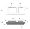
- the above-mentioned paste-like brazing material 30 is applied to the surface of the ceramic substrate 10 corresponding to almost the entire surface of one main surface and the other main surface of the ceramic substrate 10 or the portion where the metal plate 20 is joined by a method such as a screen printing method. Apply.
- the coating weight per unit area of the brazing material is preferably in the range of about 0.08 to 0.50 mg / cm 2 , and the thickness of the brazing material to be applied is about 5 to 5. It is preferably 35 ⁇ m. If the coating weight of the brazing material per unit area is lighter than this, or if the brazing material is thin, the bonding strength between the metal plate and the ceramic substrate becomes small, and the coating weight of the brazing material per unit area is heavy or the brazing material is thick. And there is a risk that the thermal shock resistance such as heat cycle characteristics will deteriorate. More preferably, the coating weight per unit area of the brazing material is 0.12 to 0.40 mg / cm 2 , and the thickness of the brazing material is 10 to 30 ⁇ m.
- the brazing material 30 applied to the ceramic substrate 10 is dried at, for example, 50 to 150 ° C., and then the metal plate 20 is placed on the surface of the brazing material 30 formed on both sides of the ceramic substrate.
- a sandwich-shaped laminate in which the metal plate 20 is in contact with the ceramic substrate 10 via the brazing material 30 is obtained, and is inserted into the vacuum furnace in this state.
- a weight is placed on the laminated body inserted in the vacuum furnace, and the metal plate 20 and the ceramic substrate 10 are joined via the brazing material 30 by heating in a vacuum atmosphere.
- the heating (bonding) temperature is preferably set to 770 to 900 ° C, and may be set to 790 to 860 ° C.
- the holding time at the joining temperature is about 10 to 120 minutes, and industrially, it is preferable to set it to 15 to 60 minutes in consideration of productivity and joining stability (small joining defects, high joining strength). Further, while the temperature is raised to the joining temperature, the binder may be held at 500 to 700 ° C. for 30 to 60 minutes to remove the organic matter in the brazing material 30.
- the laminate can be taken out from the vacuum furnace to obtain a metal-ceramic bonded substrate in which the metal plate 20 and the ceramic substrate 10 are bonded via the brazing material 30.
- the bonding area is 25 cm 2 or more, and further 36 cm, because bonding defects such as voids and unbonded are likely to occur when the bonding area is increased. It is preferable to apply to those having 2 or more.
- the circuit may be formed by a conventional method, and if necessary, the surface of the metal plate is subjected to surface treatment such as Ni plating or rust prevention treatment. You may.
- an etching resist pattern having a predetermined circuit shape or the like is formed on the metal plate 20 to form copper chloride.
- the metal plate 20 such as a copper plate is removed by performing an etching treatment with a chemical solution containing hydrogen fluoride and a hydrogen peroxide solution, and the brazing material 30 is further subjected to a brazing material 30 removal chemical solution containing hydrogen fluoride, a chelating agent, and the like. May be removed to form the metal plate 20 into a circuit shape or the like.
- Ni plating may be formed on the surface of the metal plate 20 by electroless Ni-P plating or electric Ni plating, or the metal plate 20 is rust-proofed by using a rust-preventive agent. You may.
- Example 1 As a ceramic substrate, an aluminum nitride substrate (manufactured by Tokuyama Corporation) having a size of 68 mm in length, 68 mm in width, and 0.6 mm in thickness was prepared.
- titanium powder As the titanium powder, a commercially available titanium powder having an average particle size (median diameter D50) of 26.902 ⁇ m was crushed to make the particle size finer, and then sieved (classified), and the average particle size D50 was 12. It was .130 ⁇ m.
- the average particle size (D50) of the copper powder was 7.3 ⁇ m, and the average particle size (D50) of the titanium oxide powder was 45 ⁇ m.
- the silver powder used had an average particle size (D50) of 0.5 ⁇ m.
- the average particle size (D50) was measured on a volume basis using a laser diffraction / scattering type particle size distribution measuring device (Laser Micronsizer LMS-3000 manufactured by Seishin Enterprise Co., Ltd.) and the dispersion medium was pure water. It is a thing.
- This paste-like active metal-containing brazing material was applied to the entire front and back surfaces of the aluminum nitride substrate by screen printing with a screen printing machine using a screen printing plate having an emulsion thickness of 10 ⁇ m.
- the coating amount of titanium, which is an active metal in the brazing material, per unit area was 0.271 mg / cm 2 .
- the entire front and back surfaces of the aluminum nitride substrate are covered with copper plates having a length of 70 mm, a width of 70 mm, and a thickness of 0.25 mm.
- the laminates arranged in contact with each other are prepared and inserted into a vacuum furnace, and a weight of 200 g is placed on the laminates and heated in a vacuum (vacuum degree 1.0 ⁇ 10 -4 torr or less) at 835 ° C. for 40 minutes.
- -Fifty-eight metal-ceramic bonded substrates were prepared by joining by holding and bonding copper plates to both sides of the aluminum nitride substrate via a brazing material.
- the 58 metal-ceramic bonding substrates thus obtained were coated with a bonding region (active metal brazing material) with a probe frequency of 50 MHz using an ultrasonic flaw detector (ultrasonic imaging device FS100II manufactured by Hitachi Power Solutions, Ltd.).
- the joint defect region (void portion, unjoined portion) with respect to the region) was calculated as the area ratio (referred to as the joint defect ratio).
- the average bonding defect rate was 0.321 area%, which was good with very few bonding defects.
- Titanium powder is 1.0% by mass, copper powder is 6.0% by mass, titanium oxide powder is 0.5% by mass, silver powder is 92.5% by mass, and titanium powder is sieved with respect to the total amount of the powder of the brazing material. Fine particles are selected by classification (classification), and those having a D50 particle size of 17.644 ⁇ m are used, and the same method as in Example 1 is used except that the coating amount per unit area of titanium is 0.163 mg / cm 2. A metal-ceramics bonded substrate was produced.
- the bonding defect rate was very small at 0.339 area%, and the ceramic substrate after passing through the furnace 10 times was very small. There were no cracks in the ceramics, the thermal shock resistance was good, and the joint strength was 196 N / cm, which was good.
- Titanium powder is 1.7% by mass, copper powder is 6.0% by mass, titanium oxide powder is 0.5% by mass, and silver powder is 91.8% by mass with respect to the total amount of the powder of the brazing material, and the unit area of titanium is
- a metal-ceramics bonded substrate and a metal-ceramics bonded circuit substrate were produced in the same manner as in Example 2 except that the coating amount per coating amount was 0.277 mg / cm 2.
- the bonding defect rate was very small at 0.337 area%, and the ceramic substrate after passing through the furnace 10 times was very small. There were no cracks in the cracks, the thermal impact resistance was good, and the joint strength was 247 N / cm, which was good.
- Comparative Example 1 Examples of titanium powder, except that a commercially available titanium powder having a particle size (median diameter D50) of 26.902 ⁇ m is used (without pulverization) and the coating amount per unit area of titanium is 0.270 mg / cm 2. A metal-ceramic bonded substrate was produced in the same manner as in 1.
- the bonding defect rate was 1.655 area%, and the defect area was large and not good.
- Example 2 A metal-ceramic bonded substrate was prepared in the same manner as in Example 2 except that a commercially available titanium powder having a particle size (median diameter D50) of 26.902 ⁇ m was used as the titanium powder (without pulverization).
- the bonding defect rate was 63 area%, and the defect area was very large (the unbonded region was large). It was a level that could not be used as a product of.
- Example 3 A commercially available titanium powder having a particle size (median diameter D50) of 26.902 ⁇ m was used as the titanium powder (without crushing), except that the coating amount per unit area of titanium was 0.282 mg / cm 2.
- a metal-ceramic bonded substrate was produced in the same manner as in Example 3.
- the bonding defect rate was 0.855 area%, and the defect area was large and not good.
- the bonding defect rate was 0.869 area%, and the defect area was large and not good.
- Table 1 shows the evaluation results of the above brazing material and metal-ceramic bonding substrate.
Landscapes
- Engineering & Computer Science (AREA)
- Chemical & Material Sciences (AREA)
- Mechanical Engineering (AREA)
- Materials Engineering (AREA)
- Organic Chemistry (AREA)
- Ceramic Engineering (AREA)
- Metallurgy (AREA)
- Structural Engineering (AREA)
- Ceramic Products (AREA)
Abstract
平均粒径(D50)が20μm以下であるチタン粉を0.7~2.0質量%、銅粉を3~15質量%、残部として銀粉を含む粉体と、ビヒクルとを含むペースト状のろう材およびその関連技術を提供する。
Description
本発明は、ろう材およびその製造方法並びに金属-セラミックス接合基板の製造方法に関し、金属板をセラミックス基板に接合する際に用いられる活性金属を含有するろう材とその製造方法、またこのろう材を使用して金属板をセラミックス基板に接合する金属-セラミックス接合基板の製造方法に関する。
電気自動車、電車、工作機械などに用いられる大電力を制御するためにパワーモジュールが使用されている。このようなパワーモジュール用の絶縁回路基板として、セラミックス基板の一方の面に接合されたチップ部品や端子の半田付けがなされる金属(回路)板と、セラミックス基板の他方の面に接合された放熱板を半田付けなどの方法で接合・形成するための(放熱板形成用)金属板からなる、金属-セラミックス接合基板が使用されている。
金属-セラミックス接合基板では、金属回路板や放熱板形成用金属板の材料として電気伝導率、熱伝導性の高い銅やアルミニウムが用いられることが多く、また、セラミックス基板として絶縁性の高いアルミナ基板や窒化アルミニウム基板、窒化珪素基板などが用いられる。このような金属板をセラミックス基板に接合する際、活性金属を含有するろう材を介して真空中で加熱して接合する方法、いわゆる活性金属法による接合が広く用いられている。
パワーモジュールは電車などの車両に用いられ、またパワー半導体チップの特性向上等により、高密度化、スイッチング速度の高速化が進むとともに、さらに高電圧の領域に適用されるようになってきた。金属-セラミックス接合基板に高電圧が負荷されると、接合界面に存在するボイドなどの欠陥から部分放電(コロナ放電)が発生し、それが繰り返し発生すると金属-セラミックス接合基板に絶縁破壊が生じ、パワーモジュールが壊れる恐れがある。また、前記ボイド等の(接合)欠陥は金属-セラミックス接合基板の放熱性を劣化させる恐れもある。
特許文献1には、セラミックス基板と、その少なくとも一方の面に接合された金属板とからなり、上記接合層のボイドが直径0.65mm以下であることを特徴とする金属-セラミックス接合基板が開示されており、コロナ放電を抑制し耐電圧が4kV以上となる金属-セラミックス接合基板について記載されている。
特許文献2には、セラミックス基板の主面上に接合した金属板上の半導体搭載部分の接合界面におけるボイドを面積率で1.5%以下とするセラミックス-金属複合回路基板が開示されている。また、セラミックス基板のとしてアルミナ基板を用いる旨が開示されている。接合界面のボイドが少なくなることで放熱性が改善されるとの記載がある。
近年、電車などの車両に用いられるパワーモジュールに使用される金属-セラミックス接合基板においては、1つの金属-セラミックス接合基板の金属回路板に搭載するチップの数が増え、比較的大面積で且つ接合欠陥の少ない金属-セラミックス接合基板が求められている。
しかしながら本発明者らの調査によると、特許文献1、2の金属-セラミックス接合基板およびその製造方法では、金属-セラミックス接合基板の(接合部の)面積が例えば20cm2を超える大面積のものを接合した場合は、ボイドや未接合などの接合欠陥を十分に抑制することが困難であるという課題があることがわかってきた。また、一般的に接合領域が大面積である金属とセラミックス(特にセラミックスが窒化物系である場合など)においては、小面積のものと比較すると接合欠陥を低減することは困難であることが知られている。
本発明は、このような接合領域の面積が大きい大型の金属-セラミックス接合基板においても、接合欠陥を十分に低減することを可能とする、ろう材およびその製造方法並びに金属-セラミックス基板の製造方法を提供することを目的とする。
本発明の第1の態様は、
平均粒径(D50)が20μm以下であるチタン粉を0.7~2.0質量%、銅粉を3~15質量%、残部として銀粉を含む粉体と、ビヒクルとを含むことを特徴とする、ペースト状のろう材である。
平均粒径(D50)が20μm以下であるチタン粉を0.7~2.0質量%、銅粉を3~15質量%、残部として銀粉を含む粉体と、ビヒクルとを含むことを特徴とする、ペースト状のろう材である。
本発明の第2の態様は、第1の態様に記載の態様であって、
前記チタン粉の平均粒径(D50)が5μm以上であることを特徴とする。
前記チタン粉の平均粒径(D50)が5μm以上であることを特徴とする。
本発明の第3の態様は、第1または第2の態様に記載の態様であって、
前記粉体における前記チタン粉の量が0.9~1.8質量%であることを特徴とする。
前記粉体における前記チタン粉の量が0.9~1.8質量%であることを特徴とする。
本発明の第4の態様は、第1~第3のいずれかの態様に記載の態様であって、
前記粉体における前記銅粉の量が5~13質量%であることを特徴とする。
前記粉体における前記銅粉の量が5~13質量%であることを特徴とする。
本発明の第5の態様は、第1~第4のいずれかの態様に記載の態様であって、
前記粉体としてさらに1.0質量%以下の酸化チタン粉を含むことを特徴とする。
前記粉体としてさらに1.0質量%以下の酸化チタン粉を含むことを特徴とする。
本発明の第6の態様は、
平均粒径(D50)が20μm以下であるチタン粉を0.7~2.0質量%、銅粉を3~15質量%、残部として銀粉を含む粉体を準備し、前記粉体とビヒクルを混練してペースト状にすることを特徴とする、ペースト状のろう材の製造方法である。
平均粒径(D50)が20μm以下であるチタン粉を0.7~2.0質量%、銅粉を3~15質量%、残部として銀粉を含む粉体を準備し、前記粉体とビヒクルを混練してペースト状にすることを特徴とする、ペースト状のろう材の製造方法である。
本発明の第7の態様は、第6の態様に記載の態様であって、
前記チタン粉の平均粒径(D50)が5μm以上であることを特徴とする。
前記チタン粉の平均粒径(D50)が5μm以上であることを特徴とする。
本発明の第8の態様は、第6または第7の態様に記載の態様であって、
前記粉体における前記チタン粉の量が0.9~1.8質量%であることを特徴とする。
前記粉体における前記チタン粉の量が0.9~1.8質量%であることを特徴とする。
本発明の第9の態様は、第6~第8のいずれかの態様に記載の態様であって、
前記粉体における前記銅粉の量が5~13質量%であることを特徴とする。
前記粉体における前記銅粉の量が5~13質量%であることを特徴とする。
本発明の第10の態様は、第6~第9のいずれかの態様に記載の態様であって、
前記粉体としてさらに1.0質量%以下の酸化チタン粉を含むことを特徴とする。
前記粉体としてさらに1.0質量%以下の酸化チタン粉を含むことを特徴とする。
本発明の第11の態様は、
第1~第5のいずれかの態様に記載のペースト状のろう材を使用して、金属板とセラミックス基板を接合することを特徴とする、金属-セラミックス接合基板の製造方法である。
第1~第5のいずれかの態様に記載のペースト状のろう材を使用して、金属板とセラミックス基板を接合することを特徴とする、金属-セラミックス接合基板の製造方法である。
本発明の第12の態様は、第11の態様に記載の態様であって、
前記セラミックス基板の一方の主面に前記ろう材を塗布し、塗布されたろう材に前記金属板を接触配置させ、真空雰囲気で加熱して接合することを特徴とする。
前記セラミックス基板の一方の主面に前記ろう材を塗布し、塗布されたろう材に前記金属板を接触配置させ、真空雰囲気で加熱して接合することを特徴とする。
本発明の第13の態様は、第12の態様に記載の態様であって、
さらに前記セラミックス基板の他方の主面に前記ろう材を塗布し、塗布されたろう材に金属板を接触配置させ、真空雰囲気で加熱して接合することを特徴とする。
さらに前記セラミックス基板の他方の主面に前記ろう材を塗布し、塗布されたろう材に金属板を接触配置させ、真空雰囲気で加熱して接合することを特徴とする。
本発明の第14の態様は、第11~第13のいずれかの態様に記載の態様であって、
前記金属板が銅または銅合金であることを特徴とする。
前記金属板が銅または銅合金であることを特徴とする。
本発明の第15の態様は、第11~第14のいずれかの態様に記載の態様であって、
前記セラミックス基板がアルミナ、窒化アルミニウムまたは窒化珪素から選ばれる1つを主成分とすることを特徴とする。
前記セラミックス基板がアルミナ、窒化アルミニウムまたは窒化珪素から選ばれる1つを主成分とすることを特徴とする。
本発明は、金属-セラミックス接合基板の接合欠陥を十分に低減することを可能とする、ろう材およびその製造方法並びに金属-セラミックス基板の製造方法を提供することができる。
本発明のペースト状のろう材は、平均粒径(D50)が20μm以下であるチタン粉を0.7~2.0質量%、銅粉を3~15質量%、残部として銀粉を含む粉体と、ビヒクルとを含むことを特徴とする。また、本発明のペースト状のろう材の製造方法は、平均粒径(D50)が20μm以下であるチタン粉を0.7~2.0質量%、銅粉を3~15質量%、残部として銀粉を含む粉体を準備し、前記粉体とビヒクルを混練してペースト状にすることを特徴とする。
(チタン粉)
本発明のろう材は、平均粒径(D50)が20μm以下であるチタン粉を(粉体の総量に対して)0.7~2.0質量%とする。このような微細な粒径のチタン粉を用いることにより、ペースト状のろう材をセラミックス基板に塗布したときに、平均粒径(D50)が20μmを超えるチタン粉と比べて粒径が小さいために、ろう材の塗布領域において面積当たりの(接合に寄与する)チタン粉の個数密度が高くなり、より均一にチタン粉を分布させることができ、金属板とセラミックス基板が接合される際にムラなく接合して金属-セラミックス接合基板の接合欠陥を低減することができると考えられ、また十分な接合強度を得ることができる。また、取り扱いにおける安全性の問題から、平均粒径(D50)の下限として5μm以上、さらには10μm以上とすることが好ましい。本発明においてチタン粉とは、チタン粉または水素化チタン粉を意味する。
本発明のろう材は、平均粒径(D50)が20μm以下であるチタン粉を(粉体の総量に対して)0.7~2.0質量%とする。このような微細な粒径のチタン粉を用いることにより、ペースト状のろう材をセラミックス基板に塗布したときに、平均粒径(D50)が20μmを超えるチタン粉と比べて粒径が小さいために、ろう材の塗布領域において面積当たりの(接合に寄与する)チタン粉の個数密度が高くなり、より均一にチタン粉を分布させることができ、金属板とセラミックス基板が接合される際にムラなく接合して金属-セラミックス接合基板の接合欠陥を低減することができると考えられ、また十分な接合強度を得ることができる。また、取り扱いにおける安全性の問題から、平均粒径(D50)の下限として5μm以上、さらには10μm以上とすることが好ましい。本発明においてチタン粉とは、チタン粉または水素化チタン粉を意味する。
また、チタン粉と銅粉と銀粉等を含む粉体の総量を100質量%としたときに、チタン粉の量を0.7~2.0質量%とする。チタン粉の量が少なすぎると、金属-セラミックス接合基板を作製したときに、必要な接合強度が得られず、量が多すぎると接合欠陥は低減する傾向であるが、耐熱衝撃性が低下するおそれがある。粉体に対するチタン粉の量は0.9~1.8質量%であることが好ましい。
なお、前記粉体中にチタン粉、銅粉、銀粉以外の、例えば1.0質量%以下のSn粉、In粉等の他の粉体或いは不純物成分を、本発明の効果を奏する範囲で含有してもよい。
(銅粉)
本発明のろう材は、銅粉の量が(粉体の総量に対して)3~15質量%であることを特徴とする。銅粉の量が少なすぎる或いは多すぎると接合欠陥が増加する恐れがある。銅粉の量は5~13質量%であることがより好ましい。
本発明のろう材は、銅粉の量が(粉体の総量に対して)3~15質量%であることを特徴とする。銅粉の量が少なすぎる或いは多すぎると接合欠陥が増加する恐れがある。銅粉の量は5~13質量%であることがより好ましい。
また、銅粉と銀粉によって、銅と銀の融体が形成される。この融体には、ろう材の溶融温度(接合温度)を下げる作用があり、金属-セラミックス接合基板の耐熱衝撃性を向上させる効果があると考えられる。
本発明のろう材の製造方法に用いる銅粉の平均粒径(D50)は40μm以下であることが好ましく、20μm以下であることがより好ましい。銅粉はチタン粉と異なり、金属板とセラミックス基板の接合界面に(チタンがセラミックス基板の成分と反応生成物を形成するように)反応生成物を形成しないと考えられるため、すなわち直接的には接合に寄与しないためチタン粉と比べて粒径の影響は小さいと考えられる。ただし、ろう材をスクリーン印刷などで塗布する際に、粒径が大きいと目詰まりする恐れがあるので上記粒径のものを使用するのが好ましい。銅粉の平均粒径(D50)は、さらに好ましくは0.1~10μmである。
(銀粉)
本発明のろう材は、(粉体の総量に対して)チタン粉と銅粉を除いた残部として銀粉を含むことを特徴とする。前述の通り、銅粉と銀粉によって、銅と銀の融体が形成される。この融体には、ろう材の溶融温度(接合温度)を下げる作用があり、金属-セラミックス接合基板の耐熱衝撃性を向上させる効果があると考えられる。
本発明のろう材は、(粉体の総量に対して)チタン粉と銅粉を除いた残部として銀粉を含むことを特徴とする。前述の通り、銅粉と銀粉によって、銅と銀の融体が形成される。この融体には、ろう材の溶融温度(接合温度)を下げる作用があり、金属-セラミックス接合基板の耐熱衝撃性を向上させる効果があると考えられる。
本発明のろう材の製造方法に用いる銀粉の平均粒径(D50)は40μm以下であることが好ましく、20μm以下であることがより好ましく、0.1~10μmであることがさらに好ましい。銀粉はチタン粉と異なり、金属板とセラミックス基板の接合界面に(チタンがセラミックス基板の成分と反応生成物を形成するように)反応生成物を形成しないと考えられるため、すなわち直接的には接合に寄与しないためチタン粉と比べて粒径の影響は小さいと考えられる。
(ビヒクル)
本発明のろう材は前記粉体とビヒクルとからなり、ビヒクルと前記粉体を混錬してペースト状のろう材を作製する。ビヒクルはバインダーと溶剤からなり、一般に用いられている有機系のバインダーとそれを溶解する溶剤を使用すればよい。
本発明のろう材は前記粉体とビヒクルとからなり、ビヒクルと前記粉体を混錬してペースト状のろう材を作製する。ビヒクルはバインダーと溶剤からなり、一般に用いられている有機系のバインダーとそれを溶解する溶剤を使用すればよい。
例えば、主にアクリル系バインダーやセルロース系バインダー等の有機バインダーと、α-テルピネオールやジブチルフタレート等の有機溶剤とを含むヒヒクルが挙げられ、ろう材ペースト中の金属粉末を粘結してペースト状となす作用をなす。
アクリル系バインダーとしては、例えばポリメチルメタアクリレートやポリイソブチルメタアクリレート・ポリノルマルブチルメタアクリレート等が、セルロース系バインダーとしては、エチルセルロースやメチルセルロース・ニトロセルロース等が例示できる。
このようなビヒクルの含有量等は、ペースト状のろう材に適当なチキソ性および粘度を付与するように適宜調整すればよい。例えば前記粉末の総量を100重量部としたときビヒクルを7~15重量部添加したものを、一般的な混錬手法である乳鉢や3本ロールミル、プラネタリーミキサー等を用いて混錬し、ペースト状のろう材を作製することができる。
なお、ビヒクル中のバインダーは40~60質量%、残部が溶剤であるのが好ましい。
(酸化チタン粉)
前記粉体を100質量%としたときに、前記粉体中に1.0質量%以下の酸化チタン粉を含んでもよい。酸化チタン粉を添加することにより、耐熱衝撃性の改善が見込まれるが、添加量が多いと接合欠陥が増大するので前記範囲内とするのが好ましい。酸化チタン粉の添加は粉体に対して0.1~0.6質量%としてもよい。
前記粉体を100質量%としたときに、前記粉体中に1.0質量%以下の酸化チタン粉を含んでもよい。酸化チタン粉を添加することにより、耐熱衝撃性の改善が見込まれるが、添加量が多いと接合欠陥が増大するので前記範囲内とするのが好ましい。酸化チタン粉の添加は粉体に対して0.1~0.6質量%としてもよい。
酸化チタン粉の平均粒径(D50)は、ろう材をスクリーン印刷などで塗布する際に、粒径が大きいと目詰まりする恐れがあることを考慮し、平均粒径(D50)が50μm以下であることが好ましい。
(金属-セラミックス接合基板の製造方法)
本発明の金属-セラミックス接合基板の製造方法は、前述のペースト状のろう材を使用して、金属板とセラミックス基板を接合することを特徴とする。
本発明の金属-セラミックス接合基板の製造方法は、前述のペースト状のろう材を使用して、金属板とセラミックス基板を接合することを特徴とする。
金属板は電子回路や放熱目的で使用されるため、導電率や熱伝導率に優れた銅または銅合金であることが好ましい。また、セラミックス基板は金属-セラミックス接合基板として回路用に用いることから絶縁性に優れたアルミナ、窒化アルミニウム、窒化珪素から選ばれる1種を主成分とすることが好ましい。金属板、セラミックス基板ともに市販されているものを使用することができる。
以下、図1を参照し金属-セラミックス接合基板の製造方法を説明する。
セラミックス基板10の一方の主面および他方の主面のほぼ全面或いは金属板20を接合する部分に対応するセラミックス基板10の表面に、前述のペースト状のろう材30をスクリーン印刷法等の方法で塗布する。
ろう材の組成にもよるが、ろう材の単位面積当たりの塗布重量は概ね0.08~0.50mg/cm2の範囲とすることが好ましく、また塗布するろう材の厚さは概ね5~35μmとすることが好ましい。これよりも単位面積当たりのろう材の塗布重量が軽い、あるいはろう材が薄いと金属板とセラミックス基板の接合強度が小さくなり、単位面積当たりのろう材の塗布重量が重い、あるいはろう材が厚いとヒートサイクル特性などの耐熱衝撃性が悪くなる恐れがある。さらに好ましいろう材の単位面積当たりの塗布重量は0.12~0.40mg/cm2、ろう材の厚さは10~30μmである。
セラミックス基板10に塗布したろう材30を、例えば50~150℃で乾燥させた後、金属板20をセラミックス基板の両面に形成されたろう材30の表面に配置する。このように配置することにより、セラミックス基板10にろう材30を介して金属板20が接触しているサンドイッチ状の積層体が得られ、この状態で真空炉に挿入する。
真空炉に挿入した前記積層体の上に必要に応じて重りを載せ、真空雰囲気で加熱してろう材30を介して金属板20とセラミックス基板10を接合する。加熱(接合)温度は770~900℃に設定することが好ましく、790~860℃に設定してもよい。接合温度での保持時間は10~120分程度であり、工業的には15~60分とすることが生産性と接合の安定性(接合欠陥小、接合強度大)を考慮すると好ましい。また、接合温度まで昇温する途中に例えば500~700℃で30~60分保持して、ろう材30中の有機物を除去する脱バインダーを行ってもよい。
このようにして接合した後、真空炉から積層体を取り出し、金属板20とセラミックス基板10がろう材30を介して接合された、金属-セラミックス接合基板を得ることができる。
なお、本発明の効果を有効に利用するためには、接合面積を大きくなるとボイドや未接合などの接合欠陥が発生しやすくなるので、接合面積が25cm2以上であるのが好ましく、さらには36cm2以上であるものに適用するのが好ましい。
その後、回路が形成された金属-セラミックス接合基板を得るために、従来の方法により回路を形成してもよく、必要に応じて金属板の表面にNiめっきや防錆処理等の表面処理をしてもよい。
例えば、前述のようにセラミックス基板10の全面にろう材30を塗布した上に金属板20を接合したときに、金属板20の上に所定の回路形状などのエッチングレジストパターンを形成し、塩化銅と過酸化水素水を含む薬液等によるエッチング処理を行うことで、銅板などの金属板20を除去し、さらにフッ化水素やキレート剤などを含むろう材30除去用の薬液を用いてろう材30を除去して、金属板20を回路形状等としてもよい。
また、例えば表面処理において、無電解Ni-Pめっき或いは電気Niめっきなどで金属板20の表面にNiめっきを形成してもよいし、防錆処理剤を用いて金属板20を防錆処理してもよい。
以下、本発明によるろう材およびろう材の製造方法並びに金属-セラミックス接合基板の製造方法の実施例について詳細に説明する。
[実施例1]
セラミックス基板として縦68mm、横68mm、厚さ0.6mmの大きさの窒化アルミニウム基板(株式会社トクヤマ製)を準備した。
セラミックス基板として縦68mm、横68mm、厚さ0.6mmの大きさの窒化アルミニウム基板(株式会社トクヤマ製)を準備した。
また、1.7質量%の市販のチタン粉(純度99.9質量%以上)と、10質量%の市販の銅粉(電解銅粉)と、0.5質量%の市販の酸化チタン粉(酸化チタン(IV)ルチル型)と、87.8質量%(残部)の市販の銀粉からなる粉末100gに、アクリル系のバインダーと溶剤からなるビヒクルを13.8g添加して、乳鉢および三本ロールミルを用いて混練し、ペースト状の(活性金属含有)ろう材を作製した。
なお、チタン粉は平均粒径(メジアン径D50)が26.902μmである市販のチタン粉末を粉砕して粒径を細かくしたのち篩い分け(分級)したものを用い、その平均粒径D50は12.130μmであった。
銅粉の平均粒径(D50)は7.3μm、酸化チタン粉の平均粒径(D50)は45μmのものを用いた。
銀粉は、平均粒径(D50)が0.5μmのものを用いた。
なお、上記平均粒径(D50)は、レーザー回折・散乱式粒度分布測定器(株式会社セイシン企業製、レーザーマイクロンサイザーLMS-3000)を用いて、分散媒は純水として、体積基準により測定したものである。
このペースト状の活性金属含有ろう材を、乳剤厚10μmのスクリーン印刷版を使用して、前記窒化アルミニウム基板の表と裏の面のそれぞれ全面に、スクリーン印刷機によりスクリーン印刷することにより塗布した。なお、ろう材中の活性金属であるチタンの単位面積あたりの塗布量は0.271mg/cm2であった。
次いで、窒化アルミニウム基板の表裏のそれぞれの面に塗布されたろう材を乾燥させた後、縦70mm、横70mm、厚さ0.25mmの銅板をそれぞれ窒化アルミニウム基板の表裏の主面の全部が覆われるように接触配置させた積層体を作製して真空炉に挿入し、この積層体に200gの重りを載せて真空中(真空度1.0×10⁻⁴torr以下)において835℃で40分加熱・保持することで接合し、窒化アルミニウム基板の両面にろう材を介して銅板が接合された金属-セラミックス接合基板を58個作製した。
(接合欠陥率)
このようにして得られた金属-セラミックス接合基板58個について、超音波探傷機(株式会社日立パワーソリューションズ製 超音波映像装置FS100II)により、プローブ周波数を50MHzとして接合領域(活性金属ろう材を塗布した領域)に対する接合欠陥領域(ボイド部、未接合部)を面積率(接合欠陥率という)としてそれぞれ算出した。その結果、接合欠陥率の平均は0.321面積%で接合欠陥が非常に少なく良好であった。
このようにして得られた金属-セラミックス接合基板58個について、超音波探傷機(株式会社日立パワーソリューションズ製 超音波映像装置FS100II)により、プローブ周波数を50MHzとして接合領域(活性金属ろう材を塗布した領域)に対する接合欠陥領域(ボイド部、未接合部)を面積率(接合欠陥率という)としてそれぞれ算出した。その結果、接合欠陥率の平均は0.321面積%で接合欠陥が非常に少なく良好であった。
金属-セラミックス接合基板の、一方の銅板の表面に回路形状のエッチングレジストインクを塗布し、他方の銅板の表面に長方形の放熱板接合用金属板を形成するためにセラミックス基板の外周端部から1mmの部分を除いた領域にエッチングレジストインクをスクリーン印刷により塗布した。その後、紫外線を照射して塗布したエッチングレジストインクを硬化し、薬液によりエッチングレジストが形成されていない領域の不要な銅板とろう材を除去し、エッチングレジストを除去して、金属-セラミックス接合回路基板を得た。
(耐熱衝撃性)
N2ガス:H2ガス=4:1(体積比)の還元雰囲気のバッチ炉に前記金属-セラミックス接合回路基板を投入し、金属-セラミックス接合回路基板の投入から最高温度に到達するまでの時間を6分、最高温度380℃、最高温度での保持時間10分、最高温度から炉内温度が50℃になるまでの降温時間を5分とするヒートサイクルを1回とする通炉を行い、10回通炉した後にセラミックス基板の表面のクラックの発生の有無を実体顕微鏡で観察した。その結果、クラックの発生はなく耐熱衝撃性は良好であった。この耐熱衝撃性のことを通炉耐量ともいう。
N2ガス:H2ガス=4:1(体積比)の還元雰囲気のバッチ炉に前記金属-セラミックス接合回路基板を投入し、金属-セラミックス接合回路基板の投入から最高温度に到達するまでの時間を6分、最高温度380℃、最高温度での保持時間10分、最高温度から炉内温度が50℃になるまでの降温時間を5分とするヒートサイクルを1回とする通炉を行い、10回通炉した後にセラミックス基板の表面のクラックの発生の有無を実体顕微鏡で観察した。その結果、クラックの発生はなく耐熱衝撃性は良好であった。この耐熱衝撃性のことを通炉耐量ともいう。
(接合強度)
また、金属-セラミックス接合回路基板の銅板を窒化アルミニウム基板から引き剥がしたときの接合強度を90°ピール試験により測定した結果、160N/cmであり良好であった。
また、金属-セラミックス接合回路基板の銅板を窒化アルミニウム基板から引き剥がしたときの接合強度を90°ピール試験により測定した結果、160N/cmであり良好であった。
[実施例2]
ろう材の前記粉末の総量に対するチタン粉が1.0質量%、銅粉が6.0質量%、酸化チタン粉が0.5質量%、銀粉が92.5質量%であり、チタン粉は篩い分け(分級)により細かい粒子を選択してD50粒径が17.644μmのものを用い、チタンの単位面積あたりの塗布量が0.163mg/cm2である以外は実施例1と同様の方法で金属-セラミックス接合基板を作製した。
ろう材の前記粉末の総量に対するチタン粉が1.0質量%、銅粉が6.0質量%、酸化チタン粉が0.5質量%、銀粉が92.5質量%であり、チタン粉は篩い分け(分級)により細かい粒子を選択してD50粒径が17.644μmのものを用い、チタンの単位面積あたりの塗布量が0.163mg/cm2である以外は実施例1と同様の方法で金属-セラミックス接合基板を作製した。
得られた金属-セラミックス接合基板および金属-セラミックス接合回路基板を実施例1と同様の方法で評価したところ、接合欠陥率は0.339面積%で非常に小さく、10回通炉後のセラミックス基板へのクラックの発生はなく耐熱衝撃性は良好で、接合強度は196N/cmで良好あった。
[実施例3]
ろう材の前記粉末の総量に対するチタン粉が1.7質量%、銅粉が6.0質量%、酸化チタン粉が0.5質量%、銀粉が91.8質量%であり、チタンの単位面積あたりの塗布量が0.277mg/cm2である以外は、実施例2と同様の方法で金属-セラミックス接合基板および金属-セラミックス接合回路基板を作製した。
ろう材の前記粉末の総量に対するチタン粉が1.7質量%、銅粉が6.0質量%、酸化チタン粉が0.5質量%、銀粉が91.8質量%であり、チタンの単位面積あたりの塗布量が0.277mg/cm2である以外は、実施例2と同様の方法で金属-セラミックス接合基板および金属-セラミックス接合回路基板を作製した。
得られた金属-セラミックス接合基板および金属-セラミックス接合回路基板を実施例1と同様の方法で評価したところ、接合欠陥率は0.337面積%で非常に小さく、10回通炉後のセラミックス基板へのクラックの発生はなく耐熱衝撃性は良好で、接合強度は247N/cmで良好あった。
[比較例1]
チタン粉として粒径(メジアン径D50)が26.902μmである市販のチタン粉末を(粉砕することなく)用い、チタンの単位面積あたりの塗布量が0.270mg/cm2である以外は実施例1と同様の方法で金属-セラミックス接合基板を作製した。
チタン粉として粒径(メジアン径D50)が26.902μmである市販のチタン粉末を(粉砕することなく)用い、チタンの単位面積あたりの塗布量が0.270mg/cm2である以外は実施例1と同様の方法で金属-セラミックス接合基板を作製した。
得られた金属-セラミックス接合基板を実施例1と同様の方法で評価したところ、接合欠陥率は1.659面積%であり欠陥面積が大きく良好でなかった。
[比較例2]
チタン粉として粒径(メジアン径D50)が26.902μmである市販のチタン粉末を(粉砕することなく)用いた以外は、実施例2と同様の方法で金属-セラミックス接合基板を作製した。
チタン粉として粒径(メジアン径D50)が26.902μmである市販のチタン粉末を(粉砕することなく)用いた以外は、実施例2と同様の方法で金属-セラミックス接合基板を作製した。
得られた金属-セラミックス接合基板を実施例1と同様の方法で評価したところ、接合欠陥率は63面積%であり欠陥面積が非常に大きく(接合していない領域が大きく)金属-セラミックス接合基板の製品としては使用できないレベルであった。
[比較例3]
チタン粉として粒径(メジアン径D50)が26.902μmである市販のチタン粉末を(粉砕することなく)用い、チタンの単位面積あたりの塗布量が0.282mg/cm2である以外は、実施例3と同様の方法で金属-セラミックス接合基板を作製した。
チタン粉として粒径(メジアン径D50)が26.902μmである市販のチタン粉末を(粉砕することなく)用い、チタンの単位面積あたりの塗布量が0.282mg/cm2である以外は、実施例3と同様の方法で金属-セラミックス接合基板を作製した。
得られた金属-セラミックス接合基板を実施例1と同様の方法で評価したところ、接合欠陥率は0.855面積%であり欠陥面積が大きく良好ではなかった。
[比較例4]
ろう材の前記粉末の総量に対するチタン粉が1.7質量%、銅粉が16.0質量%、酸化チタン粉が0.5質量%、銀粉が81.8質量%である以外は、実施例3と同様の方法で金属-セラミックス接合基板を作製した。
ろう材の前記粉末の総量に対するチタン粉が1.7質量%、銅粉が16.0質量%、酸化チタン粉が0.5質量%、銀粉が81.8質量%である以外は、実施例3と同様の方法で金属-セラミックス接合基板を作製した。
得られた金属-セラミックス接合基板を実施例1と同様の方法で評価したところ、接合欠陥率は0.869面積%であり欠陥面積が大きく良好ではなかった。
以上のろう材および金属-セラミックス接合基板の評価結果を表1に示す。

10 セラミックス基板
20 金属板
30 ろう材
20 金属板
30 ろう材
Claims (15)
- 平均粒径(D50)が20μm以下であるチタン粉を0.7~2.0質量%、銅粉を3~15質量%、残部として銀粉を含む粉体と、ビヒクルとを含むことを特徴とする、ペースト状のろう材。
- 前記チタン粉の平均粒径(D50)が5μm以上であることを特徴とする、請求項1に記載のろう材。
- 前記粉体における前記チタン粉の量が0.9~1.8質量%であることを特徴とする、請求項1または2に記載のろう材。
- 前記粉体における前記銅粉の量が5~13質量%であることを特徴とする、請求項1~3のいずれかに記載のろう材。
- 前記粉体としてさらに1.0質量%以下の酸化チタン粉を含むことを特徴とする、請求項1~4のいずれかに記載のろう材。
- 平均粒径(D50)が20μm以下であるチタン粉を0.7~2.0質量%、銅粉を3~15質量%、残部として銀粉を含む粉体を準備し、前記粉体とビヒクルを混練してペースト状にすることを特徴とする、ペースト状のろう材の製造方法。
- 前記チタン粉の平均粒径(D50)が5μm以上であることを特徴とする、請求項6に記載のろう材の製造方法。
- 前記粉体における前記チタン粉の量が0.9~1.8質量%であることを特徴とする、請求項6または7に記載のろう材の製造方法。
- 前記粉体における前記銅粉の量が5~13質量%であることを特徴とする、請求項6~8のいずれかに記載のろう材の製造方法。
- 前記粉体としてさらに1.0質量%以下の酸化チタン粉を含むことを特徴とする、請求項6~9のいずれかに記載のろう材の製造方法。
- 請求項1~5のいずれかに記載のペースト状のろう材を使用して、金属板とセラミックス基板を接合することを特徴とする、金属-セラミックス接合基板の製造方法。
- 前記セラミックス基板の一方の主面に前記ろう材を塗布し、塗布されたろう材に前記金属板を接触配置させ、真空雰囲気で加熱して接合することを特徴とする、請求項11に記載の金属-セラミックス接合基板の製造方法。
- さらに前記セラミックス基板の他方の主面に前記ろう材を塗布し、塗布されたろう材に金属板を接触配置させ、真空雰囲気で加熱して接合することを特徴とする、請求項12に記載の金属-セラミックス接合基板の製造方法。
- 前記金属板が銅または銅合金であることを特徴とする、請求項11~13のいずれかに記載の金属-セラミックス接合基板の製造方法。
- 前記セラミックス基板がアルミナ、窒化アルミニウムまたは窒化珪素から選ばれる1つを主成分とすることを特徴とする、請求項11~14のいずれかに記載の金属-セラミックス接合基板の製造方法。
Priority Applications (4)
| Application Number | Priority Date | Filing Date | Title |
|---|---|---|---|
| CN202180016354.3A CN115151371A (zh) | 2020-03-31 | 2021-03-18 | 硬钎焊材料和其制造方法以及金属-陶瓷接合基板的制造方法 |
| US17/914,853 US12337421B2 (en) | 2020-03-31 | 2021-03-18 | Brazing material, method for producing the same, and method for producing metal-ceramics bonded substrate |
| KR1020227020061A KR20220156516A (ko) | 2020-03-31 | 2021-03-18 | 브레이징재 및 그 제조 방법 그리고 금속-세라믹스 접합 기판의 제조 방법 |
| EP21778786.0A EP4130308A4 (en) | 2020-03-31 | 2021-03-18 | SOLDER MATERIAL, METHOD FOR PRODUCING SAME AND METHOD FOR PRODUCING A METAL-CERAMIC COMPOSITE SUBSTRATE |
Applications Claiming Priority (2)
| Application Number | Priority Date | Filing Date | Title |
|---|---|---|---|
| JP2020061887A JP7537900B2 (ja) | 2020-03-31 | 2020-03-31 | ろう材およびその製造方法並びに金属-セラミックス接合基板の製造方法 |
| JP2020-061887 | 2020-03-31 |
Publications (1)
| Publication Number | Publication Date |
|---|---|
| WO2021200242A1 true WO2021200242A1 (ja) | 2021-10-07 |
Family
ID=77928576
Family Applications (1)
| Application Number | Title | Priority Date | Filing Date |
|---|---|---|---|
| PCT/JP2021/011235 Ceased WO2021200242A1 (ja) | 2020-03-31 | 2021-03-18 | ろう材およびその製造方法並びに金属-セラミックス接合基板の製造方法 |
Country Status (6)
| Country | Link |
|---|---|
| US (1) | US12337421B2 (ja) |
| EP (1) | EP4130308A4 (ja) |
| JP (1) | JP7537900B2 (ja) |
| KR (1) | KR20220156516A (ja) |
| CN (1) | CN115151371A (ja) |
| WO (1) | WO2021200242A1 (ja) |
Cited By (4)
| Publication number | Priority date | Publication date | Assignee | Title |
|---|---|---|---|---|
| WO2023286862A1 (ja) * | 2021-07-16 | 2023-01-19 | 三菱マテリアル株式会社 | 銅/セラミックス接合体、および、絶縁回路基板 |
| WO2023176045A1 (ja) * | 2022-03-14 | 2023-09-21 | Dowaメタルテック株式会社 | 銅-セラミックス接合基板およびその製造方法 |
| EP4253348A1 (en) * | 2022-03-29 | 2023-10-04 | Proterial, Ltd. | Ceramic substrate, ceramic divided substrate, and method for manufacturing ceramic substrate |
| US20250010408A1 (en) * | 2023-07-06 | 2025-01-09 | Tong Hsing Electronic Industries, Ltd. | Active metal brazing substrate material containing aluminum metal element and method for producing the same |
Families Citing this family (3)
| Publication number | Priority date | Publication date | Assignee | Title |
|---|---|---|---|---|
| JP7739105B2 (ja) * | 2021-09-21 | 2025-09-16 | Dowaメタルテック株式会社 | 金属-セラミックス接合基板およびその製造方法 |
| KR102911157B1 (ko) * | 2023-06-29 | 2026-01-12 | (주)창성 | 금속-세라믹 접합용 페이스트 |
| CN117415511A (zh) * | 2023-11-21 | 2024-01-19 | 苏州铜宝锐新材料有限公司 | 用于陶瓷覆铜连接的铜基钎焊材料及其应用 |
Citations (8)
| Publication number | Priority date | Publication date | Assignee | Title |
|---|---|---|---|---|
| JPH09188582A (ja) * | 1995-11-08 | 1997-07-22 | Dowa Mining Co Ltd | 金属−セラミックス複合基板の製造方法並びにそれに用いるろう材 |
| JPH09283671A (ja) | 1996-04-12 | 1997-10-31 | Dowa Mining Co Ltd | セラミックス−金属複合回路基板 |
| JPH1129371A (ja) * | 1997-07-10 | 1999-02-02 | Tokuyama Corp | ろう材および窒化アルミニウム部材と金属部材との接合方法 |
| JP2000246482A (ja) * | 1999-02-26 | 2000-09-12 | Kyocera Corp | ろう材ペースト |
| JP2001048671A (ja) | 1999-08-13 | 2001-02-20 | Dowa Mining Co Ltd | 金属−セラミックス接合基板 |
| WO2016013651A1 (ja) * | 2014-07-24 | 2016-01-28 | 電気化学工業株式会社 | ろう材及びこれを用いたセラミック基板 |
| JP2018145047A (ja) * | 2017-03-03 | 2018-09-20 | Dowaメタルテック株式会社 | 金属−セラミックス回路基板の製造方法 |
| WO2020105734A1 (ja) * | 2018-11-22 | 2020-05-28 | デンカ株式会社 | セラミックス-銅複合体、セラミックス-銅複合体の製造方法、セラミックス回路基板およびパワーモジュール |
Family Cites Families (14)
| Publication number | Priority date | Publication date | Assignee | Title |
|---|---|---|---|---|
| JPH0570260A (ja) * | 1991-09-18 | 1993-03-23 | Murata Mfg Co Ltd | セラミツクと金属の接合用ロウペースト |
| JP3997293B2 (ja) * | 1995-12-06 | 2007-10-24 | Dowaメタルテック株式会社 | 点接合または線接合を有する金属−セラミックス複合基板の製造方法 |
| US5955686A (en) * | 1996-10-30 | 1999-09-21 | Dowa Mining Co., Ltd. | Brazing materials for producing metal-ceramics composite substrates |
| JP3682552B2 (ja) | 1997-03-12 | 2005-08-10 | 同和鉱業株式会社 | 金属−セラミックス複合基板の製造方法 |
| JPH11130555A (ja) * | 1997-10-28 | 1999-05-18 | Kyocera Corp | セラミックス−銅接合用ろう材 |
| JP4168114B2 (ja) * | 2001-09-28 | 2008-10-22 | Dowaホールディングス株式会社 | 金属−セラミックス接合体 |
| JP5128829B2 (ja) * | 2007-02-28 | 2013-01-23 | Dowaメタルテック株式会社 | 金属−セラミックス接合基板およびそれに用いるろう材 |
| JP2009234895A (ja) * | 2008-03-28 | 2009-10-15 | Dowa Metaltech Kk | 金属−セラミックス接合基板の製造方法 |
| EP2727898B1 (en) * | 2011-06-30 | 2017-02-01 | Hitachi Metals, Ltd. | Brazing filler metal, brazing filler metal paste, ceramic circuit substrate, and ceramic master circuit substrate |
| JP6100501B2 (ja) * | 2012-10-31 | 2017-03-22 | デンカ株式会社 | セラミック回路基板および製造方法 |
| JP5741971B2 (ja) * | 2013-09-30 | 2015-07-01 | Dowaメタルテック株式会社 | 金属−セラミックス接合回路基板の製造方法 |
| JP2017041567A (ja) | 2015-08-20 | 2017-02-23 | デンカ株式会社 | セラミックス回路基板の製造方法 |
| US11570890B2 (en) * | 2017-05-30 | 2023-01-31 | Denka Company Limited | Ceramic circuit board and module using same |
| JP6750056B2 (ja) | 2019-02-27 | 2020-09-02 | 東邦チタニウム株式会社 | チタン粉の製造方法、スポンジチタンの製造方法、チタン粉および、ガス収集装置 |
-
2020
- 2020-03-31 JP JP2020061887A patent/JP7537900B2/ja active Active
-
2021
- 2021-03-18 CN CN202180016354.3A patent/CN115151371A/zh active Pending
- 2021-03-18 US US17/914,853 patent/US12337421B2/en active Active
- 2021-03-18 EP EP21778786.0A patent/EP4130308A4/en active Pending
- 2021-03-18 KR KR1020227020061A patent/KR20220156516A/ko active Pending
- 2021-03-18 WO PCT/JP2021/011235 patent/WO2021200242A1/ja not_active Ceased
Patent Citations (8)
| Publication number | Priority date | Publication date | Assignee | Title |
|---|---|---|---|---|
| JPH09188582A (ja) * | 1995-11-08 | 1997-07-22 | Dowa Mining Co Ltd | 金属−セラミックス複合基板の製造方法並びにそれに用いるろう材 |
| JPH09283671A (ja) | 1996-04-12 | 1997-10-31 | Dowa Mining Co Ltd | セラミックス−金属複合回路基板 |
| JPH1129371A (ja) * | 1997-07-10 | 1999-02-02 | Tokuyama Corp | ろう材および窒化アルミニウム部材と金属部材との接合方法 |
| JP2000246482A (ja) * | 1999-02-26 | 2000-09-12 | Kyocera Corp | ろう材ペースト |
| JP2001048671A (ja) | 1999-08-13 | 2001-02-20 | Dowa Mining Co Ltd | 金属−セラミックス接合基板 |
| WO2016013651A1 (ja) * | 2014-07-24 | 2016-01-28 | 電気化学工業株式会社 | ろう材及びこれを用いたセラミック基板 |
| JP2018145047A (ja) * | 2017-03-03 | 2018-09-20 | Dowaメタルテック株式会社 | 金属−セラミックス回路基板の製造方法 |
| WO2020105734A1 (ja) * | 2018-11-22 | 2020-05-28 | デンカ株式会社 | セラミックス-銅複合体、セラミックス-銅複合体の製造方法、セラミックス回路基板およびパワーモジュール |
Non-Patent Citations (1)
| Title |
|---|
| See also references of EP4130308A4 |
Cited By (4)
| Publication number | Priority date | Publication date | Assignee | Title |
|---|---|---|---|---|
| WO2023286862A1 (ja) * | 2021-07-16 | 2023-01-19 | 三菱マテリアル株式会社 | 銅/セラミックス接合体、および、絶縁回路基板 |
| WO2023176045A1 (ja) * | 2022-03-14 | 2023-09-21 | Dowaメタルテック株式会社 | 銅-セラミックス接合基板およびその製造方法 |
| EP4253348A1 (en) * | 2022-03-29 | 2023-10-04 | Proterial, Ltd. | Ceramic substrate, ceramic divided substrate, and method for manufacturing ceramic substrate |
| US20250010408A1 (en) * | 2023-07-06 | 2025-01-09 | Tong Hsing Electronic Industries, Ltd. | Active metal brazing substrate material containing aluminum metal element and method for producing the same |
Also Published As
| Publication number | Publication date |
|---|---|
| KR20220156516A (ko) | 2022-11-25 |
| JP2021159926A (ja) | 2021-10-11 |
| US20230068210A1 (en) | 2023-03-02 |
| CN115151371A (zh) | 2022-10-04 |
| US12337421B2 (en) | 2025-06-24 |
| JP7537900B2 (ja) | 2024-08-21 |
| EP4130308A4 (en) | 2024-05-01 |
| EP4130308A1 (en) | 2023-02-08 |
Similar Documents
| Publication | Publication Date | Title |
|---|---|---|
| JP7537900B2 (ja) | ろう材およびその製造方法並びに金属-セラミックス接合基板の製造方法 | |
| JP5725178B2 (ja) | ろう材、ろう材ペースト、セラミックス回路基板、セラミックスマスター回路基板及びパワー半導体モジュール | |
| EP2811513B1 (en) | Method for producing substrate for power modules | |
| EP2816593B1 (en) | Solder joint structure, power module, heat-sink-attached substrate for power module, method for producing said substrate, and paste for forming solder underlayer | |
| CN103492345B (zh) | 陶瓷电路基板 | |
| EP3632879A1 (en) | Ceramic circuit board and module using same | |
| EP2930744B1 (en) | Substrate for power modules, substrate with heat sink for power modules and power module | |
| CN110691762B (zh) | 陶瓷电路基板和其制造方法 | |
| JP2005112677A (ja) | セラミックス基板用ろう材及びこれを用いたセラミックス回路基板 | |
| JP4632116B2 (ja) | セラミックス回路基板 | |
| JP5915233B2 (ja) | はんだ接合構造、パワーモジュール、ヒートシンク付パワーモジュール用基板及びそれらの製造方法 | |
| KR101887290B1 (ko) | 접합 구조 및 전자부재 접합 구조체 | |
| JP6565527B2 (ja) | Ag下地層付パワーモジュール用基板及びパワーモジュール | |
| WO2016052392A1 (ja) | Ag下地層付パワーモジュール用基板及びパワーモジュール | |
| JP2013125779A (ja) | はんだ接合構造、パワーモジュール、放熱板付パワーモジュール用基板及び冷却器付パワーモジュール用基板 | |
| JP2006120973A (ja) | 回路基板および回路基板の製造方法 | |
| EP4640363A1 (en) | Metal paste composition and metal-ceramic composite substrate comprising the same | |
| JP2553268B2 (ja) | 窒化アルミニウム焼結体の製造方法 | |
| TW202448602A (zh) | 低溫燒結性接合用材料及接合結構體 | |
| JP2001019576A (ja) | 基板およびその製造方法 | |
| JPH0361353B2 (ja) |
Legal Events
| Date | Code | Title | Description |
|---|---|---|---|
| 121 | Ep: the epo has been informed by wipo that ep was designated in this application |
Ref document number: 21778786 Country of ref document: EP Kind code of ref document: A1 |
|
| NENP | Non-entry into the national phase |
Ref country code: DE |
|
| ENP | Entry into the national phase |
Ref document number: 2021778786 Country of ref document: EP Effective date: 20221031 |
|
| WWG | Wipo information: grant in national office |
Ref document number: 17914853 Country of ref document: US |