WO2021200406A1 - 半導体装置 - Google Patents
半導体装置 Download PDFInfo
- Publication number
- WO2021200406A1 WO2021200406A1 PCT/JP2021/012062 JP2021012062W WO2021200406A1 WO 2021200406 A1 WO2021200406 A1 WO 2021200406A1 JP 2021012062 W JP2021012062 W JP 2021012062W WO 2021200406 A1 WO2021200406 A1 WO 2021200406A1
- Authority
- WO
- WIPO (PCT)
- Prior art keywords
- semiconductor device
- glass substrate
- hole
- frame
- insulating film
- Prior art date
- Legal status (The legal status is an assumption and is not a legal conclusion. Google has not performed a legal analysis and makes no representation as to the accuracy of the status listed.)
- Ceased
Links
Images


Classifications
-
- H—ELECTRICITY
- H10—SEMICONDUCTOR DEVICES; ELECTRIC SOLID-STATE DEVICES NOT OTHERWISE PROVIDED FOR
- H10W—GENERIC PACKAGES, INTERCONNECTIONS, CONNECTORS OR OTHER CONSTRUCTIONAL DETAILS OF DEVICES COVERED BY CLASS H10
- H10W70/00—Package substrates; Interposers; Redistribution layers [RDL]
- H10W70/60—Insulating or insulated package substrates; Interposers; Redistribution layers
- H10W70/67—Insulating or insulated package substrates; Interposers; Redistribution layers characterised by their insulating layers or insulating parts
- H10W70/69—Insulating materials thereof
- H10W70/692—Ceramics or glasses
-
- H—ELECTRICITY
- H01—ELECTRIC ELEMENTS
- H01Q—ANTENNAS, i.e. RADIO AERIALS
- H01Q1/00—Details of, or arrangements associated with, antennas
- H01Q1/36—Structural form of radiating elements, e.g. cone, spiral, umbrella; Particular materials used therewith
- H01Q1/38—Structural form of radiating elements, e.g. cone, spiral, umbrella; Particular materials used therewith formed by a conductive layer on an insulating support
-
- H—ELECTRICITY
- H10—SEMICONDUCTOR DEVICES; ELECTRIC SOLID-STATE DEVICES NOT OTHERWISE PROVIDED FOR
- H10F—INORGANIC SEMICONDUCTOR DEVICES SENSITIVE TO INFRARED RADIATION, LIGHT, ELECTROMAGNETIC RADIATION OF SHORTER WAVELENGTH OR CORPUSCULAR RADIATION
- H10F39/00—Integrated devices, or assemblies of multiple devices, comprising at least one element covered by group H10F30/00, e.g. radiation detectors comprising photodiode arrays
- H10F39/80—Constructional details of image sensors
- H10F39/804—Containers or encapsulations
-
- H—ELECTRICITY
- H10—SEMICONDUCTOR DEVICES; ELECTRIC SOLID-STATE DEVICES NOT OTHERWISE PROVIDED FOR
- H10P—GENERIC PROCESSES OR APPARATUS FOR THE MANUFACTURE OR TREATMENT OF DEVICES COVERED BY CLASS H10
- H10P72/00—Handling or holding of wafers, substrates or devices during manufacture or treatment thereof
- H10P72/70—Handling or holding of wafers, substrates or devices during manufacture or treatment thereof for supporting or gripping
- H10P72/74—Handling or holding of wafers, substrates or devices during manufacture or treatment thereof for supporting or gripping using temporarily an auxiliary support
-
- H—ELECTRICITY
- H10—SEMICONDUCTOR DEVICES; ELECTRIC SOLID-STATE DEVICES NOT OTHERWISE PROVIDED FOR
- H10W—GENERIC PACKAGES, INTERCONNECTIONS, CONNECTORS OR OTHER CONSTRUCTIONAL DETAILS OF DEVICES COVERED BY CLASS H10
- H10W40/00—Arrangements for thermal protection or thermal control
- H10W40/20—Arrangements for cooling
- H10W40/22—Arrangements for cooling characterised by their shape, e.g. having conical or cylindrical projections
- H10W40/226—Arrangements for cooling characterised by their shape, e.g. having conical or cylindrical projections characterised by projecting parts, e.g. fins to increase surface area
- H10W40/228—Arrangements for cooling characterised by their shape, e.g. having conical or cylindrical projections characterised by projecting parts, e.g. fins to increase surface area the projecting parts being wire-shaped or pin-shaped
-
- H—ELECTRICITY
- H10—SEMICONDUCTOR DEVICES; ELECTRIC SOLID-STATE DEVICES NOT OTHERWISE PROVIDED FOR
- H10W—GENERIC PACKAGES, INTERCONNECTIONS, CONNECTORS OR OTHER CONSTRUCTIONAL DETAILS OF DEVICES COVERED BY CLASS H10
- H10W42/00—Arrangements for protection of devices
- H10W42/121—Arrangements for protection of devices protecting against mechanical damage
-
- H—ELECTRICITY
- H10—SEMICONDUCTOR DEVICES; ELECTRIC SOLID-STATE DEVICES NOT OTHERWISE PROVIDED FOR
- H10W—GENERIC PACKAGES, INTERCONNECTIONS, CONNECTORS OR OTHER CONSTRUCTIONAL DETAILS OF DEVICES COVERED BY CLASS H10
- H10W44/00—Electrical arrangements for controlling or matching impedance
- H10W44/20—Electrical arrangements for controlling or matching impedance at high-frequency [HF] or radio frequency [RF]
-
- H—ELECTRICITY
- H10—SEMICONDUCTOR DEVICES; ELECTRIC SOLID-STATE DEVICES NOT OTHERWISE PROVIDED FOR
- H10W—GENERIC PACKAGES, INTERCONNECTIONS, CONNECTORS OR OTHER CONSTRUCTIONAL DETAILS OF DEVICES COVERED BY CLASS H10
- H10W46/00—Marks applied to devices, e.g. for alignment or identification
-
- H—ELECTRICITY
- H10—SEMICONDUCTOR DEVICES; ELECTRIC SOLID-STATE DEVICES NOT OTHERWISE PROVIDED FOR
- H10W—GENERIC PACKAGES, INTERCONNECTIONS, CONNECTORS OR OTHER CONSTRUCTIONAL DETAILS OF DEVICES COVERED BY CLASS H10
- H10W70/00—Package substrates; Interposers; Redistribution layers [RDL]
- H10W70/01—Manufacture or treatment
- H10W70/05—Manufacture or treatment of insulating or insulated package substrates, or of interposers, or of redistribution layers
- H10W70/095—Manufacture or treatment of insulating or insulated package substrates, or of interposers, or of redistribution layers of vias therein
-
- H—ELECTRICITY
- H10—SEMICONDUCTOR DEVICES; ELECTRIC SOLID-STATE DEVICES NOT OTHERWISE PROVIDED FOR
- H10W—GENERIC PACKAGES, INTERCONNECTIONS, CONNECTORS OR OTHER CONSTRUCTIONAL DETAILS OF DEVICES COVERED BY CLASS H10
- H10W90/00—Package configurations
-
- H—ELECTRICITY
- H10—SEMICONDUCTOR DEVICES; ELECTRIC SOLID-STATE DEVICES NOT OTHERWISE PROVIDED FOR
- H10F—INORGANIC SEMICONDUCTOR DEVICES SENSITIVE TO INFRARED RADIATION, LIGHT, ELECTROMAGNETIC RADIATION OF SHORTER WAVELENGTH OR CORPUSCULAR RADIATION
- H10F39/00—Integrated devices, or assemblies of multiple devices, comprising at least one element covered by group H10F30/00, e.g. radiation detectors comprising photodiode arrays
- H10F39/80—Constructional details of image sensors
- H10F39/811—Interconnections
-
- H—ELECTRICITY
- H10—SEMICONDUCTOR DEVICES; ELECTRIC SOLID-STATE DEVICES NOT OTHERWISE PROVIDED FOR
- H10P—GENERIC PROCESSES OR APPARATUS FOR THE MANUFACTURE OR TREATMENT OF DEVICES COVERED BY CLASS H10
- H10P72/00—Handling or holding of wafers, substrates or devices during manufacture or treatment thereof
- H10P72/70—Handling or holding of wafers, substrates or devices during manufacture or treatment thereof for supporting or gripping
- H10P72/74—Handling or holding of wafers, substrates or devices during manufacture or treatment thereof for supporting or gripping using temporarily an auxiliary support
- H10P72/7424—Handling or holding of wafers, substrates or devices during manufacture or treatment thereof for supporting or gripping using temporarily an auxiliary support used as a support during the manufacture of self-supporting substrates
-
- H—ELECTRICITY
- H10—SEMICONDUCTOR DEVICES; ELECTRIC SOLID-STATE DEVICES NOT OTHERWISE PROVIDED FOR
- H10W—GENERIC PACKAGES, INTERCONNECTIONS, CONNECTORS OR OTHER CONSTRUCTIONAL DETAILS OF DEVICES COVERED BY CLASS H10
- H10W44/00—Electrical arrangements for controlling or matching impedance
- H10W44/20—Electrical arrangements for controlling or matching impedance at high-frequency [HF] or radio frequency [RF]
- H10W44/241—Electrical arrangements for controlling or matching impedance at high-frequency [HF] or radio frequency [RF] for passive devices or passive elements
- H10W44/248—Electrical arrangements for controlling or matching impedance at high-frequency [HF] or radio frequency [RF] for passive devices or passive elements for antennas
-
- H—ELECTRICITY
- H10—SEMICONDUCTOR DEVICES; ELECTRIC SOLID-STATE DEVICES NOT OTHERWISE PROVIDED FOR
- H10W—GENERIC PACKAGES, INTERCONNECTIONS, CONNECTORS OR OTHER CONSTRUCTIONAL DETAILS OF DEVICES COVERED BY CLASS H10
- H10W46/00—Marks applied to devices, e.g. for alignment or identification
- H10W46/301—Marks applied to devices, e.g. for alignment or identification for alignment
-
- H—ELECTRICITY
- H10—SEMICONDUCTOR DEVICES; ELECTRIC SOLID-STATE DEVICES NOT OTHERWISE PROVIDED FOR
- H10W—GENERIC PACKAGES, INTERCONNECTIONS, CONNECTORS OR OTHER CONSTRUCTIONAL DETAILS OF DEVICES COVERED BY CLASS H10
- H10W46/00—Marks applied to devices, e.g. for alignment or identification
- H10W46/601—Marks applied to devices, e.g. for alignment or identification for use after dicing
- H10W46/607—Located on parts of packages, e.g. on encapsulations or on package substrates
-
- H—ELECTRICITY
- H10—SEMICONDUCTOR DEVICES; ELECTRIC SOLID-STATE DEVICES NOT OTHERWISE PROVIDED FOR
- H10W—GENERIC PACKAGES, INTERCONNECTIONS, CONNECTORS OR OTHER CONSTRUCTIONAL DETAILS OF DEVICES COVERED BY CLASS H10
- H10W70/00—Package substrates; Interposers; Redistribution layers [RDL]
- H10W70/099—Connecting interconnections to insulating or insulated package substrates, interposers or redistribution layers
-
- H—ELECTRICITY
- H10—SEMICONDUCTOR DEVICES; ELECTRIC SOLID-STATE DEVICES NOT OTHERWISE PROVIDED FOR
- H10W—GENERIC PACKAGES, INTERCONNECTIONS, CONNECTORS OR OTHER CONSTRUCTIONAL DETAILS OF DEVICES COVERED BY CLASS H10
- H10W70/00—Package substrates; Interposers; Redistribution layers [RDL]
- H10W70/60—Insulating or insulated package substrates; Interposers; Redistribution layers
- H10W70/62—Insulating or insulated package substrates; Interposers; Redistribution layers characterised by their interconnections
- H10W70/63—Vias, e.g. via plugs
- H10W70/635—Through-vias
-
- H—ELECTRICITY
- H10—SEMICONDUCTOR DEVICES; ELECTRIC SOLID-STATE DEVICES NOT OTHERWISE PROVIDED FOR
- H10W—GENERIC PACKAGES, INTERCONNECTIONS, CONNECTORS OR OTHER CONSTRUCTIONAL DETAILS OF DEVICES COVERED BY CLASS H10
- H10W70/00—Package substrates; Interposers; Redistribution layers [RDL]
- H10W70/60—Insulating or insulated package substrates; Interposers; Redistribution layers
- H10W70/67—Insulating or insulated package substrates; Interposers; Redistribution layers characterised by their insulating layers or insulating parts
- H10W70/68—Shapes or dispositions thereof
- H10W70/682—Shapes or dispositions thereof comprising holes having chips therein
-
- H—ELECTRICITY
- H10—SEMICONDUCTOR DEVICES; ELECTRIC SOLID-STATE DEVICES NOT OTHERWISE PROVIDED FOR
- H10W—GENERIC PACKAGES, INTERCONNECTIONS, CONNECTORS OR OTHER CONSTRUCTIONAL DETAILS OF DEVICES COVERED BY CLASS H10
- H10W70/00—Package substrates; Interposers; Redistribution layers [RDL]
- H10W70/60—Insulating or insulated package substrates; Interposers; Redistribution layers
- H10W70/67—Insulating or insulated package substrates; Interposers; Redistribution layers characterised by their insulating layers or insulating parts
- H10W70/69—Insulating materials thereof
-
- H—ELECTRICITY
- H10—SEMICONDUCTOR DEVICES; ELECTRIC SOLID-STATE DEVICES NOT OTHERWISE PROVIDED FOR
- H10W—GENERIC PACKAGES, INTERCONNECTIONS, CONNECTORS OR OTHER CONSTRUCTIONAL DETAILS OF DEVICES COVERED BY CLASS H10
- H10W72/00—Interconnections or connectors in packages
- H10W72/071—Connecting or disconnecting
- H10W72/072—Connecting or disconnecting of bump connectors
- H10W72/07221—Aligning
- H10W72/07223—Active alignment, e.g. using optical alignment using marks or sensors
-
- H—ELECTRICITY
- H10—SEMICONDUCTOR DEVICES; ELECTRIC SOLID-STATE DEVICES NOT OTHERWISE PROVIDED FOR
- H10W—GENERIC PACKAGES, INTERCONNECTIONS, CONNECTORS OR OTHER CONSTRUCTIONAL DETAILS OF DEVICES COVERED BY CLASS H10
- H10W72/00—Interconnections or connectors in packages
- H10W72/071—Connecting or disconnecting
- H10W72/073—Connecting or disconnecting of die-attach connectors
- H10W72/07321—Aligning
- H10W72/07323—Active alignment, e.g. using optical alignment using marks or sensors
-
- H—ELECTRICITY
- H10—SEMICONDUCTOR DEVICES; ELECTRIC SOLID-STATE DEVICES NOT OTHERWISE PROVIDED FOR
- H10W—GENERIC PACKAGES, INTERCONNECTIONS, CONNECTORS OR OTHER CONSTRUCTIONAL DETAILS OF DEVICES COVERED BY CLASS H10
- H10W72/00—Interconnections or connectors in packages
- H10W72/071—Connecting or disconnecting
- H10W72/075—Connecting or disconnecting of bond wires
- H10W72/07521—Aligning
- H10W72/07523—Active alignment, e.g. using optical alignment using marks or sensors
-
- H—ELECTRICITY
- H10—SEMICONDUCTOR DEVICES; ELECTRIC SOLID-STATE DEVICES NOT OTHERWISE PROVIDED FOR
- H10W—GENERIC PACKAGES, INTERCONNECTIONS, CONNECTORS OR OTHER CONSTRUCTIONAL DETAILS OF DEVICES COVERED BY CLASS H10
- H10W72/00—Interconnections or connectors in packages
- H10W72/071—Connecting or disconnecting
- H10W72/075—Connecting or disconnecting of bond wires
- H10W72/07541—Controlling the environment, e.g. atmosphere composition or temperature
- H10W72/07554—Controlling the environment, e.g. atmosphere composition or temperature changes in dispositions
-
- H—ELECTRICITY
- H10—SEMICONDUCTOR DEVICES; ELECTRIC SOLID-STATE DEVICES NOT OTHERWISE PROVIDED FOR
- H10W—GENERIC PACKAGES, INTERCONNECTIONS, CONNECTORS OR OTHER CONSTRUCTIONAL DETAILS OF DEVICES COVERED BY CLASS H10
- H10W72/00—Interconnections or connectors in packages
- H10W72/851—Dispositions of multiple connectors or interconnections
- H10W72/874—On different surfaces
- H10W72/884—Die-attach connectors and bond wires
-
- H—ELECTRICITY
- H10—SEMICONDUCTOR DEVICES; ELECTRIC SOLID-STATE DEVICES NOT OTHERWISE PROVIDED FOR
- H10W—GENERIC PACKAGES, INTERCONNECTIONS, CONNECTORS OR OTHER CONSTRUCTIONAL DETAILS OF DEVICES COVERED BY CLASS H10
- H10W72/00—Interconnections or connectors in packages
- H10W72/90—Bond pads, in general
- H10W72/941—Dispositions of bond pads
- H10W72/9413—Dispositions of bond pads on encapsulations
-
- H—ELECTRICITY
- H10—SEMICONDUCTOR DEVICES; ELECTRIC SOLID-STATE DEVICES NOT OTHERWISE PROVIDED FOR
- H10W—GENERIC PACKAGES, INTERCONNECTIONS, CONNECTORS OR OTHER CONSTRUCTIONAL DETAILS OF DEVICES COVERED BY CLASS H10
- H10W76/00—Containers; Fillings or auxiliary members therefor; Seals
- H10W76/10—Containers or parts thereof
- H10W76/17—Containers or parts thereof characterised by their materials
- H10W76/18—Insulating materials, e.g. resins, glasses or ceramics
-
- H—ELECTRICITY
- H10—SEMICONDUCTOR DEVICES; ELECTRIC SOLID-STATE DEVICES NOT OTHERWISE PROVIDED FOR
- H10W—GENERIC PACKAGES, INTERCONNECTIONS, CONNECTORS OR OTHER CONSTRUCTIONAL DETAILS OF DEVICES COVERED BY CLASS H10
- H10W90/00—Package configurations
- H10W90/701—Package configurations characterised by the relative positions of pads or connectors relative to package parts
- H10W90/721—Package configurations characterised by the relative positions of pads or connectors relative to package parts of bump connectors
- H10W90/724—Package configurations characterised by the relative positions of pads or connectors relative to package parts of bump connectors between a chip and a stacked insulating package substrate, interposer or RDL
-
- H—ELECTRICITY
- H10—SEMICONDUCTOR DEVICES; ELECTRIC SOLID-STATE DEVICES NOT OTHERWISE PROVIDED FOR
- H10W—GENERIC PACKAGES, INTERCONNECTIONS, CONNECTORS OR OTHER CONSTRUCTIONAL DETAILS OF DEVICES COVERED BY CLASS H10
- H10W90/00—Package configurations
- H10W90/701—Package configurations characterised by the relative positions of pads or connectors relative to package parts
- H10W90/731—Package configurations characterised by the relative positions of pads or connectors relative to package parts of die-attach connectors
- H10W90/734—Package configurations characterised by the relative positions of pads or connectors relative to package parts of die-attach connectors between a chip and a stacked insulating package substrate, interposer or RDL
-
- H—ELECTRICITY
- H10—SEMICONDUCTOR DEVICES; ELECTRIC SOLID-STATE DEVICES NOT OTHERWISE PROVIDED FOR
- H10W—GENERIC PACKAGES, INTERCONNECTIONS, CONNECTORS OR OTHER CONSTRUCTIONAL DETAILS OF DEVICES COVERED BY CLASS H10
- H10W90/00—Package configurations
- H10W90/701—Package configurations characterised by the relative positions of pads or connectors relative to package parts
- H10W90/751—Package configurations characterised by the relative positions of pads or connectors relative to package parts of bond wires
- H10W90/754—Package configurations characterised by the relative positions of pads or connectors relative to package parts of bond wires between a chip and a stacked insulating package substrate, interposer or RDL
Definitions
- This disclosure relates to semiconductor devices.
- the glass substrate can apply semiconductor processing technology and has high surface flatness, it is promising as a substrate for semiconductor devices such as optical parts and high-frequency parts.
- semiconductor devices such as optical parts and high-frequency parts.
- it is necessary to maintain the flatness of the glass substrate and suppress cracking at the end. Therefore, it is important to protect the glass substrate.
- vias and wiring layers were formed on a glass substrate in a panel state or a wafer state, and then individualized in a dicing process.
- the stress due to the curing shrinkage of the resin used for the wiring layer is large, and if the residual stress of the resin is released at once in the dicing step of individualization, cracks may occur on the glass side surface and vias.
- CMOS Complementary Metal Oxide Semiconductor
- the present disclosure provides a semiconductor device capable of reducing the stress applied to the glass substrate and sufficiently protecting the end portion of the glass substrate.
- the semiconductor device on one side of the present disclosure includes a glass substrate including a first surface, a second surface opposite the first surface, and a first surface between the first surface and the second surface.
- the wiring provided on the first and second surfaces, the first insulating film covering the first surface, the second insulating film covering the second surface, and the first side surface are covered with the first and second surfaces.
- a third insulating film continuous with at least one of the insulating films is provided.
- the first to third insulating films may be continuously provided on the first side surface, the first surface, and the second surface.
- the first to third insulating films may be made of the same material.
- a part of the wiring may come into direct contact with the glass substrate on the first and second surfaces.
- the number of wiring layers and the number of first insulating film layers on the first surface may be the same as the number of wiring layers and the number of second insulating film layers on the second surface.
- a first metal film that covers the inner wall of the through hole that penetrates the glass substrate between the first surface and the second surface, and a fourth insulating film that is filled inside the first metal film in the through hole are further formed.
- the fourth insulating film may be made of the same material as the first and second insulating films and may be continuous.
- a part of the wiring that is in direct contact with the glass substrate may be opened on the through hole.
- the side surface of the third insulating film may be flat.
- a frame provided outside the third insulating film on the first side surface may be further provided.
- the frame has a third surface on the first surface side, a fourth surface on the second surface side, and a second side surface facing the first side surface, and the first insulating film is from the first surface to the first surface.
- the second insulating film may be continuously provided over three surfaces, and the second insulating film may be continuously provided over the second to fourth surfaces.
- a second metal film provided on the third surface of the frame and a third metal film provided on the fourth surface of the frame may be further provided.
- the frame may be made of a material having a coefficient of linear expansion substantially equal to the coefficient of linear expansion of the glass substrate.
- the first side surface of the glass substrate may have a curved surface shape that protrudes outward in a cross section in the direction perpendicular to the first surface.
- the first side surface of the glass substrate has a curved surface shape that protrudes outward in a cross section perpendicular to the first surface, and the inner side surface of the through hole also has a curved surface shape in a cross section perpendicular to the first surface. It has a curved shape that protrudes inward of the through hole, and the curvature of the first side surface may be substantially equal to the curvature of the inner surface of the through hole.
- a metal plate provided in a second through hole penetrating the glass substrate between the first surface and the second surface, and a first and second insulating films provided between the second through hole and the metal plate.
- a fifth insulating film continuous with at least one of the two may be further provided.
- the inner wall surface of the second through hole and the side surface of the metal plate may be inclined with respect to the first surface or the second surface.
- An alignment mark provided on the first surface of the glass substrate may be further provided.
- the second and third metal films may be used as an antenna for wireless communication.
- An antenna may be mounted on the first surface of the glass substrate.
- a semiconductor chip may be mounted on the first surface of the glass substrate.
- the semiconductor chip may be an image sensor chip.
- a glass substrate having fastening holes, wiring layers provided on the first and second surfaces, a semiconductor chip provided above the glass substrate, a housing provided around the semiconductor chip, and a housing.
- the provided lens and a fastener for fastening the glass substrate and the housing through the fastening hole are provided.
- the fastening hole is larger than the outer edge of the head of the fastener.
- a filler may be further provided to fill the space between the fastener and the fastening hole.
- the fastening hole may be connected to the outside on the side surface of the glass substrate.
- a plurality of fastening holes are provided on the glass substrate, and the centers of gravity of the plurality of fastening holes may overlap the semiconductor chip in a plan view from the fastening direction.
- the fastener may be fastened to the housing and the glass substrate so that the optical axis of the lens and the optical axis of the semiconductor chip are substantially aligned with each other.
- the glass substrate may have a through hole penetrating between the first surface and the second surface, provided in the through hole, connected to any of the wirings, and further provided with electronic components.
- the frame may have a through hole penetrating between the third surface and the fourth surface, provided in the through hole, connected to any of the wirings, and further provided with electronic components.
- the glass substrate may have a counterbore provided on the first surface, be provided in the counterbore, be connected to any of the wirings, and further include electronic components.
- the frame has a counterbore provided on the third surface, may be provided in the counterbore, connected to any of the wirings, and further provided with electronic components.
- a plurality of electronic components having different thicknesses are provided in the through holes, and the surfaces of the plurality of electronic components may be aligned on the first surface.
- a plurality of electronic components having different thicknesses are provided in the through holes, and the surfaces of the plurality of electronic components may be aligned on the first surface.
- a plurality of electronic components having different thicknesses are provided in each of a plurality of counterbore with different depths, and the surfaces of the plurality of electronic components may be aligned on the first surface.
- a plurality of electronic components having different thicknesses are provided in each of a plurality of counterbore with different depths, and the surfaces of the plurality of electronic components may be aligned on the first surface.
- the glass substrate has a through hole penetrating between the first surface and the second surface, is provided in the through hole, further includes a heat radiating member having the second through hole, and the electronic component has the second through hole. It may be provided inside.
- a heat radiating member provided in the through hole and having a second counterbore may be further provided, and the electronic component may be provided in the second counterbore.
- a glass frame having one end directly connected to the first surface of the glass substrate and provided so as to surround the periphery of the semiconductor chip, and a cover glass connected to the other end of the glass frame to cover the upper part of the semiconductor chip are further provided. May be good.
- a glass frame having one end directly connected to the first surface of the glass substrate and provided so as to surround the periphery of the semiconductor chip, and a cover glass connected to the other end of the glass frame to cover the upper part of the semiconductor chip are further provided. May be good.
- the glass frame and the cover glass may be integrally formed.
- the glass frame and the cover glass may be integrally formed.
- the glass frame and cover glass may be made of the same material as the glass substrate.
- the glass frame and cover glass may be made of the same material as the glass substrate.
- a light-shielding film provided on a part of the surface of the glass frame and the cover glass may be further provided.
- a light-shielding film provided on a part of the surface of the glass frame and the cover glass may be further provided.
- FIG. 6 is a schematic cross-sectional view showing a configuration example of a semiconductor device according to a modified example of the first embodiment.
- FIG. 6 is a schematic cross-sectional view showing a configuration example of GIP according to the second embodiment.
- FIG. 6 is a schematic cross-sectional view showing a configuration example of one end of the GIP according to the third embodiment.
- the schematic cross-sectional view which shows the structural example of the through silicon via of GIP by 3rd Embodiment.
- FIG. 8 is a schematic cross-sectional view showing a method of manufacturing GIP
- FIG. 9 is a schematic cross-sectional view showing a method of manufacturing GIP
- FIG. 10 is a schematic cross-sectional view showing a method of manufacturing GIP
- FIG. 11 is a schematic cross-sectional view showing a method of manufacturing GIP
- FIG. 12 is a schematic cross-sectional view showing a method of manufacturing GIP
- FIG. 13 is a schematic cross-sectional view showing a method of manufacturing GIP, following FIG. FIG.
- FIG. 14 is a schematic cross-sectional view showing a method of manufacturing GIP, following FIG.
- the cross-sectional view which shows an example of the manufacturing method of GIP of 2nd Embodiment.
- the cross-sectional view which shows the structural example of GIP of 4th Embodiment.
- FIG. 5 is a cross-sectional view showing an example of a boundary portion between an opening and a metal plate.
- FIG. 5 is a cross-sectional view showing an example of an application using GIP according to the above embodiment.
- FIG. 6 is a cross-sectional view showing another example of an application using GIP according to the above embodiment.
- FIG. 5 is a cross-sectional view showing a configuration example of a semiconductor device according to a fifth embodiment.
- FIG. 5 is a cross-sectional view showing a configuration example of a semiconductor device according to a sixth embodiment.
- FIG. 5 is a cross-sectional view showing a configuration example of a semiconductor device according to the seventh embodiment.
- FIG. 5 is a cross-sectional view showing a configuration example of a semiconductor device according to a modified example of the seventh embodiment.
- FIG. 5 is a cross-sectional view showing a configuration example of a semiconductor device according to the eighth embodiment.
- FIG. 5 is a cross-sectional view showing a configuration example of a semiconductor device according to a modified example of the eighth embodiment.
- FIG. 5 is a cross-sectional view showing a configuration example of a semiconductor device according to a ninth embodiment.
- FIG. 5 is a cross-sectional view showing a configuration example of a semiconductor device according to the tenth embodiment.
- FIG. 5 is a cross-sectional view showing a method of manufacturing a semiconductor device according to the tenth embodiment.
- FIG. 5 is a cross-sectional view showing a configuration example of a semiconductor device according to a modified example of the tenth embodiment.
- FIG. 5 is a cross-sectional view showing a configuration example of a semiconductor device according to the eleventh embodiment.
- FIG. 5 is a cross-sectional view showing a method of manufacturing a semiconductor device according to the eleventh embodiment.
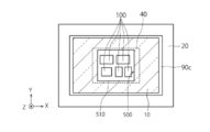
- FIG. 2 is a cross-sectional view showing a configuration example of a semiconductor device according to the twelfth embodiment.
- the plan view which shows the structural example of the semiconductor device by 12th Embodiment.
- FIG. 5 is a cross-sectional view showing a configuration example of a semiconductor device according to the thirteenth embodiment.
- the cross-sectional view which shows the structural example of the semiconductor device by 14th Embodiment.
- FIG. 6 is a cross-sectional view showing a configuration example of a semiconductor device according to a modified example of the 14th embodiment.
- FIG. 5 is a cross-sectional view showing a configuration example of a semiconductor device according to the fifteenth embodiment.
- FIG. 5 is a cross-sectional view showing a configuration example of a semiconductor device according to the 16th embodiment.
- the cross-sectional view which shows the structural example of the semiconductor device by 17th Embodiment.
- FIG. 5 is a cross-sectional view showing a configuration example of a semiconductor device according to the eighteenth embodiment.
- FIG. 5 is a cross-sectional view showing an example of a semiconductor device according to the nineteenth embodiment.
- FIG. 2 is a cross-sectional view showing an example of a semiconductor device according to the twentieth embodiment.
- FIG. 5 is a cross-sectional view showing a configuration example of a semiconductor device according to a modified example of the twentieth embodiment.
- FIG. 5 is a cross-sectional view showing a configuration example of a semiconductor device according to another modification of the 20th embodiment. The figure which shows the example which used the embodiment which concerns on this technology as a CMOS image sensor.
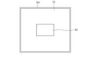
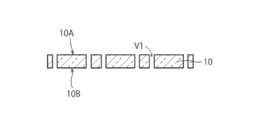
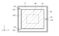
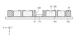
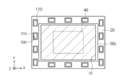
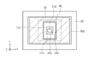
- FIG. 1 is a schematic plan view showing a configuration example of a semiconductor device (hereinafter, also referred to as a package or a module) according to the first embodiment.
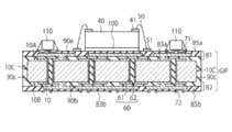
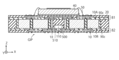
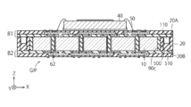
- FIG. 2 is a schematic cross-sectional view showing a configuration example of the semiconductor device according to the first embodiment. Note that FIG. 1 shows the positional relationship between the glass substrate 10, the insulating film 90c, and the semiconductor chip 40, and the detailed configuration of the through electrodes and the like is not shown.
- the semiconductor chip 40 is mounted on the central portion of the glass substrate 10.
- An insulating film 90c is provided around the glass substrate 10 so as to continuously cover the entire side surface of the glass substrate 10.
- the semiconductor chip 40 is not particularly limited, but may be, for example, a CMOS image sensor chip.
- the glass substrate 10 has a first surface 10A, a second surface 10B on the opposite side of the first surface, and a side surface (first surface) between the first surface 10A and the second surface 10B.
- Side surface Includes 10C.
- a laminated wiring portion 81 is provided on the first surface 10A.
- the laminated wiring portion 81 includes a plurality of layers of wiring 83a provided on the first surface 10A.
- the wiring 83a is covered with insulating films 85a and 90a.
- the laminated wiring portion 82 includes a plurality of layers of wiring 83b provided on the second surface 10B.
- the wiring 83b is covered with insulating films 85b and 90b.
- a low resistance metal material such as copper is used for example.
- a part of the wiring 83a is electrically connected to the electrode pad 71 on the first surface 10A.
- a part of the wiring 83b is electrically connected to the electrode pad 72 on the second surface 10B.
- the electrode pads 71 and 72 are connected to an electronic component 110 or the like, or are connected to another substrate or component (not shown).
- the other part of the wiring 83a is electrically connected to the bonding pad 51, and is electrically connected to the semiconductor chip 40 via the bonding pad 51 and the bonding wire 50.
- a part of the wiring 83a is provided on the first surface 10A of the glass substrate 10 so as to be in direct contact with the glass substrate 10, and an insulating film 90a is provided so as to cover a part of the wiring 83a. ..
- the insulating film 90a as the first insulating film covers the first surface 10A and the wiring 83a, a part of which is in contact with the first surface 10A, and the other portion is in contact with the wiring 83a. ..
- the wiring 83a that comes into direct contact with the glass substrate 10 can be used as an alignment mark in the subsequent process. In this case, it is not necessary to use the outer edge of the glass substrate 10 as the alignment mark. Therefore, the patterning of the laminated wiring portions 81 and 82 or the mounting of the semiconductor chip 40 can be performed with higher accuracy.
- a part of the wiring 83b is provided on the second surface 10B of the glass substrate 10 so as to be in direct contact with the glass substrate 10, and an insulating film 90b is provided so as to cover a part of the wiring 83b. ..
- the insulating film 90b as the second insulating film covers the second surface 10B and the wiring 83b, a part of which is in contact with the second surface 10B, and the other portion is in contact with the wiring 83b. ..
- An insulating film 90c is provided on the side surface 10C of the glass substrate 10. As shown in FIG. 1, the insulating film 90c as the third insulating film is provided on the entire outer circumference of the glass substrate 10. Further, as shown in FIG. 2, the insulating film 90c is provided so as to cover the entire side surface 10C from the first surface 10A to the second surface 10B.
- the insulating film 90c is continuous with at least one of the insulating films 90a and 90b, and is seamlessly connected. Alternatively, the insulating films 90a to 90c may be continuously and seamlessly connected to the entire first surface 10A, second surface 10B, and first side surface 10C.
- an insulating resin material such as an epoxy resin is used, and the insulating films 90a to 90c are made of the same material.
- the insulating film 90c covers the side surface 10C of the glass substrate 10 and is continuously connected to at least one of the insulating films 90a and 90b to protect the first surface 10A or the second surface 10B of the glass substrate 10. There is. Thereby, the insulating films 90a to 90c can protect the end portion and the side surface 10C of the glass substrate 10.
- the side surface 10C of the glass substrate 10 is substantially flat.
- the insulating film 90c is also substantially flat. As a result, the thickness of the insulating film 90c becomes substantially uniform, and stress concentration on the glass substrate 10 can be suppressed.
- the glass substrate 10 is provided with a through electrode 60.
- the through silicon via 60 includes a metal film 61 that covers the inner wall of a through hole (TGV (Through Glass Via)) that penetrates between the first surface 10A and the second surface 10B of the glass substrate 10, and the inside of the metal film 61. It has an insulating film 62 to be filled in.
- a low resistance metal material such as copper is used.
- the metal film 61 is continuously connected to the wirings 83a and 83b, and is preferably made of the same material as the wirings 83a and 83b.
- the metal film 61 is provided to electrically connect a part of the wiring 83 and a part of the wiring 84 via vias.
- the insulating film 62 as the fourth insulating film is continuously connected to the insulating films 90a and 90b, and is preferably made of the same material as the insulating films 90a to 90c. That is, for the insulating film 62, for example, an insulating material such as an epoxy resin is used. As a result, the insulating films 90a to 90c and 62 can be formed at the same time in the same process, and can be seamlessly configured as a continuous insulating film.
- the wiring layers 83a and 83b and the metal film 61 are seamlessly coated from the inner wall of the via to the periphery of the opening end, and the insulating films 90a to 90c and 62 are seamlessly and continuously filled from the inside to the outside of the via. Therefore, the stress generated on the TGV machined surface can be reduced and the TGV can be reinforced, and the TGV strength can be improved.
- a wiring 83a and an insulating film 85a are further provided on the insulating film 90a on the first surface 10A of the glass substrate 10.
- the laminated wiring portion 81 has a multilayer wiring structure.
- a wiring 83b and an insulating film 85b are further provided on the insulating film 90b on the second surface 10B of the glass substrate 10.
- the laminated wiring portion 82 also has a multilayer wiring structure.
- An electrode pad 71 and a bonding pad 51 are connected to the wiring 83a, and an electrode pad 72 or a bonding pad (not shown) is connected to the wiring 83b.
- a semiconductor chip 40 and an electronic component 110 are mounted on the glass substrate 10.
- the bonding pad 41 of the semiconductor chip 40 is connected to the bonding pad 51 via the bonding wire 50.
- the electronic component 110 is connected to the electrode pad 71.
- the semiconductor chip 40 is adhered on the insulating film 85a by the adhesive 100.
- this embodiment may be configured as a glass interposer (hereinafter, also simply referred to as GIP) on which the semiconductor chip 40 and the electronic component 110 are not yet mounted.
- GIP glass interposer
- the insulating film 90c covers the side surface 10C of the glass substrate 10 and is continuous with at least one of the insulating film 90a on the first surface 10A or the insulating film 90b on the second surface 10B of the glass substrate 10. Are connected. Thereby, the insulating films 90a to 90c can protect the end portion and the side surface 10C of the glass substrate 10.
- the laminated wiring portion 81 and the laminated wiring portion 82 are similarly layered, and have the same number of layers of the wiring layer and the same number of layers of the insulating layer. Further, it is preferable that the thickness of each wiring layer and the thickness of each insulating layer are substantially equal in the laminated wiring portion 81 and the laminated wiring portion 82. Therefore, the laminated wiring portion 81 and the laminated wiring portion 82 have a substantially symmetrical configuration, and substantially the same stress is applied to the glass substrate 10. Thereby, the distortion of the glass substrate 10 can be suppressed.
- the wiring patterns of the laminated wiring portion 81 and the laminated wiring portion 82 may be different.
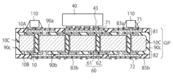
- FIG. 3 is a schematic cross-sectional view showing a configuration example of a semiconductor device according to a modified example of the first embodiment.
- the semiconductor chip 40 is flip-chip connected to a substrate for a semiconductor device.
- the semiconductor chip 40 has a metal bump 43 and is connected to the laminated wiring portion 81 by the metal bump 43. That is, in this modification, the semiconductor chip 40 is flip-chip connected above the glass substrate 10.
- Other configurations of this modification may be the same as the corresponding configurations of the first embodiment. Therefore, this modification can obtain the same effect as that of the first embodiment.
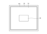
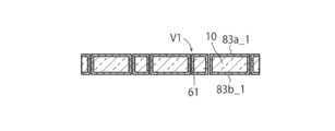
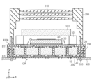
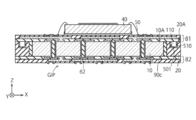
- FIG. 4 is a schematic plan view showing a configuration example of GIP according to the second embodiment.
- FIG. 5 is a schematic cross-sectional view showing a configuration example of GIP according to the second embodiment.
- the GIP of the second embodiment may be applied to either the first embodiment or a modification thereof.
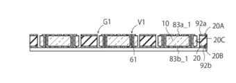
- the GIP of the second embodiment further includes a frame 20 on the side surface 10C of the glass substrate 10 and outside the insulating film 90c.
- the frame 20 is a frame-shaped member provided so as to face the entire side surface 10C over the outer periphery of the glass substrate 10.
- the frame 20 is adhered by an insulating film 90c on the side surface 10C of the glass substrate 10.
- the frame 20 has a third surface 20A, a fourth surface 20B, and a side surface (second side surface) 20C between the third surface 20A and the fourth surface 20B.
- the side surface 20C is an inner side surface of the frame 20 and is a surface facing the side surface 10C.
- the frame 20 is adhered to the insulating film 90c on the side surface 20C.
- the frame 20 is provided so as to surround the entire outer edge of the glass substrate 10, and protects the side surface 10C of the glass substrate 10 together with the insulating film 90c.
- the third surface 20A of the frame 20 is a frame surface on the first surface 10A side of the glass substrate 10.
- the fourth surface 20B of the frame 20 is a frame surface on the second surface 10B side of the glass substrate 10.
- the insulating film 90c is provided between the side surface 10C of the glass substrate 10 and the side surface 20C of the frame 20.
- the frame 20 is made of a material having a linear expansion coefficient close to that of the glass substrate 10.
- an insulating resin material such as glass epoxy resin is used.
- a first metal film 92a and a second metal film 92b are formed on the third surface 20A and the fourth surface 20B of the frame 20.
- the metal films 92a and 92b are formed by depositing a metal film on the surface of the frame 20 by a plating method and then patterning the metal film by using a lithography technique or the like.
- insulating films 90a, 90b, 85a and 85b are provided on the metal films 92a and 92b.
- the insulating film 90a is continuously provided from the first surface 10A of the glass substrate 10 to the metal film 92a.
- the insulating film 90b is continuously provided from the second surface 10B of the glass substrate 10 to the metal film 92b.
- the insulating film 85a is provided on the insulating film 90a, and is continuously provided from above the first surface 10A of the glass substrate 10 to above the metal film 92a.
- the insulating film 85b is provided on the insulating film 90b, and is continuously provided from above the second surface 10B of the glass substrate 10 to above the metal film 92b.
- the second embodiment can obtain the same effect as the first embodiment.
- the frame 20 is provided on the outside of the insulating film 90c along the side surface 10C of the glass substrate 10. Thereby, in the second embodiment, the end portion and the side surface 10C of the glass substrate 10 can be more reliably protected.
- this GIP when used for a CMOS image sensor, stray light can be blocked by the frame 20 covering the side surface 10C.
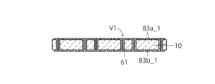
- FIG. 6 is a schematic cross-sectional view showing a configuration example of one end of the GIP according to the third embodiment.
- the side surface 10C of the glass substrate 10 has a curved surface shape that projects outward in a cross section in the direction perpendicular to the first surface 10A. This is because the dicing is performed using a laser and wet etching when the GIP is fragmented. Wet etching is performed by irradiating the glass substrate 10 with a short pulse laser in the thickness direction to modify it.
- the modified portion is selectively etched, and the corners of the side surface 10C of the glass substrate 10 are rounded due to the difference in exposure time to the etching solution, and the side surface 10C is formed into a curved surface shape protruding outward. As a result, stress concentration and microcracks that cause chipping and cracking at the edges of the glass substrate 10 can be reduced.
- FIG. 7 is a schematic cross-sectional view showing a configuration example of the through silicon via of the GIP according to the third embodiment.
- the inner side surface of the via V1 of the through electrode 60 may also have a curved surface shape as in the side surface 10C.
- the via V1 of the through electrode 60 is formed by laser and wit etching as in dicing, the inner surface of the via V1 projects inward of the via V1 in a cross section perpendicular to the first surface 10A. It has a curved shape. That is, the corners of the via V1 provided on the glass substrate 10 are rounded, and when viewed from the glass substrate 10, the via V1 is formed into a curved surface shape protruding outward from the glass substrate 10. As a result, it is possible to further suppress chipping and cracking of the end portion of the glass substrate 10 in the through electrode 60.
- the curvature of the curved surface of the inner surface of the through electrode 60 is substantially equal to the curvature of the curved surface of the side surface 10C. That is, the cross-sectional shape of the inner surface of the through electrode 60 is substantially the same as the cross-sectional shape of the side surface 10C. In this case, it is not necessary to separately prepare the process recipes for dicing and via formation, and the process can be simplified.
- FIG 8 to 15 are schematic cross-sectional views showing an example of the GIP manufacturing method of the first embodiment.
- the glass substrate 10 has a first surface 10A and a second surface 10B.
- the glass substrate 10 has not yet been diced and does not have the first side surface 10C at this stage. That is, the glass substrate 10 is in a glass panel state at this stage.
- via V1 is formed as a through hole (TGV) penetrating the glass substrate 10 between the first surface 10A and the second surface 10B.
- the via V1 is formed at the position of the through electrode 60.
- the via V1 is formed using, for example, laser processing technology and etching technology.
- a series of modified points arranged in the thickness direction of the glass substrate 10 is formed by laser light, and then the glass substrate 10 is somewhat etched by wet etching.
- the inner side surface of the via V1 is rounded into a curved surface shape, and chipping or cracking of the end portion of the through electrode 60 can be suppressed.
- a metal film is formed on the inner wall surfaces of the first surface 10A, the second surface 10B, and the via V1.
- the metal film is made of a low resistance metal such as copper and is formed by plating.
- the metal film 83a_1 which is the lower layer of the wiring 83a is formed on the first surface 10A
- the metal film 83b_1 which is the lower layer of the wiring 83b is formed on the second surface 10B.
- a metal film 61 is formed on the inner wall surface of the via V1.
- the wirings 83a and 83b and the metal film 61 are in direct contact with the surface of the glass substrate 10.
- the metal films 83a_1 and 83b_1 are processed into a predetermined wiring pattern.
- the metal films 83a_1 and 83b_1 may be patterned by using a laser processing technique.
- the metal films 83a_1 and 83b_1 may be patterned using a lithography technique and an etching technique.
- the wiring 83a that comes into direct contact with the first surface 10A of the glass substrate 10 can be used as an alignment mark.
- the patterning of the laminated wiring portions 81 and 82 can be performed with higher accuracy.
- the glass plate-shaped glass substrate 10 is diced and individualized so as to be suitable for each semiconductor device.
- dicing for example, laser processing technology and etching technology may be used as in the case of via V1.
- the glass substrate 10 is diced with a laser beam, and then the glass substrate 10 is somewhat etched using wet etching.
- the side surface 10C of the glass substrate 10 has a curved surface shape that projects outward. As a result, it is possible to suppress chipping and cracking of the end portion of the glass substrate 10.
- each piece of glass substrate 10 is arranged in the frame 20 on the support substrate.
- Metal films 92a and 92b are provided in advance on the third surface 20A and the fourth surface 30B of the frame 20.
- the frame 20 is formed in a mesh shape, and individual glass substrates 10 are placed inside the mesh.
- the inner side surface 20C of the frame 20 faces the side surface 10C of the glass substrate 10, and a gap G1 is provided between the side surface 20C and the side surface 10C.
- the gap G1 may have a width that allows the material of the insulating film 90c to be poured and can absorb the stress generated from the deformation difference between the glass substrate 10 and the frame 20, and is as small as possible in order to reduce the package size of the semiconductor device. The narrower one is preferable.
- a resin material is laminated on the first surface 10A of the glass substrate 10 and the third surface 20A of the frame 20.
- the resin material is in the form of a film and can flow by heating. Therefore, the resin material also flows into the via V1 and also into the gap G1 between the side surface 20C of the frame 20 and the side surface 10C of the glass substrate 10.
- the insulating film 90a is formed on the first surface 10A, the insulating film 62 is filled inside the metal film 61 in the via V1, and the insulating film 90c is filled in the gap G1.
- the resin material flows into the via V1 and the gap G1 and then is temporarily cured by heat treatment.
- the insulating film 90a covers the metal film 83a_1 on the first surface 10A and protects the metal film 83a_1. Further, the insulating film 90c is filled in the gap G1 to fix the frame 20 to the glass substrate 10.
- the insulating film 62 protects the metal film 61 by filling the via V1. The metal film 61 and the insulating film 62 form a through electrode 60 in the via V1.
- the metal film 83a_1 is not provided above the opening of the via V1 and is open. This is because the metal film 83a_1 is prevented from closing the opening of the via V1 so that the resin material can flow into the via V1.
- the metal film 83b_1 is not provided below the opening of the via V1 and is open. This is because the metal film 83b_1 is prevented from closing the opening of the via V1 on the second surface 10B side, and the resin material can flow into the via V1 from the second surface 10B side. As a result, the glass substrate 10 in the vicinity of the via V1 can be strengthened in terms of strength. Therefore, in order to pour the resin material into the via V1, the metal films 83a_1 and 83b_1 are not provided above or below the opening of the via V1.
- the insulating films 90a, 90c, 62 are formed in the same process using the same resin material (for example, epoxy resin or the like). Therefore, the insulating films 90a, 90c, 62 can be formed as seamlessly continuous insulating films. Thereby, the insulating films 90a, 90c, 62 and the frame 20 can surely protect the glass substrate 10.
- the resin material is laminated from the second surface 10B side of the glass substrate 10. It is preferable that the resin material is sufficiently filled in the via V1 and the gap G1 from the first surface 10A, and in this case, it is sufficient that the resin material is laminated on the second surface 10B. After that, the resin material is temporarily cured. As a result, the insulating film 90b is formed on the second surface 10B. The insulating film 90b is formed after the insulating films 90a, 90c, and 62, and is formed individually. At this point, the insulating film 90b and the insulating films 90a, 90c, 62 are in a temporarily cured state. After that, it is finally cured by further heating.
- the insulating film 90b and the insulating films 90a, 90c, 62 are made of the same material, and the joint portion can be melted during the main curing to be formed almost seamlessly and continuously. As a result, the end portion of the glass substrate 10 can be protected, and the stress applied to the glass substrate 10 is also reduced. Further, the insulating films 90a and 90b are less likely to be peeled off from the glass substrate 10.
- the effect of the present embodiment is not lost even if there is a joint between them. That is, if the insulating film 90c is continuously connected to at least one of the insulating films 90a and 90b, at least one end of the glass substrate 10 is protected, and the glass substrate 10 can be protected from stress.
- the insulating films 90a and 90b are processed into a predetermined pattern to expose a part of the metal films 83a_1 and 83b_1.
- the insulating films 90a and 90b may be via-processed by using a laser processing technique.
- the insulating films 90a and 90b may be patterned using a lithography technique and an etching technique.
- the metal film 83a_2 which is the upper layer of the wiring 83a, is deposited and patterned on the insulating film 90a and the metal film 83a_1. Further, the insulating film 85a is deposited and patterned on the metal film 83a_2. In this way, the laminated wiring portion 81 is formed by repeating the deposition and processing of the metal film 83a_2 and the insulating film 85a.
- the metal film 83b_2 which is the upper layer of the wiring 83b, is deposited and patterned on the insulating film 90b and the metal film 83b_1. Further, the insulating film 85b is deposited and patterned on the metal film 83b_2. In this way, the laminated wiring portion 82 is formed by repeating the deposition and processing of the metal film 83b_2 and the insulating film 85b.
- the number, film thickness and material of the metal films 83a_1, 83a_2 and the insulating films 90a and 85a on the first surface 10A side of the glass substrate 10 are the layers of the metal films 83b_1, 83b_2 and the insulating films 90b and 85b on the second surface 10B side. It is preferably approximately equal in number, film thickness and material. As a result, the stress applied to the glass substrate 10 from the laminated wiring portions 81 and 82 becomes substantially equal, and the distortion of the glass substrate 10 can be suppressed.
- the GIP including the glass substrate 10 is separated by dicing between the frame 20 and the insulating film 90c.
- Dicing may be performed using a laser processing technique or a dicing blade.
- dicing is performed between the side surface 20c of the frame 20 and the side surface 10C of the glass substrate 10.
- the insulating film 90c remains on the side surface of the glass substrate 10, but the frame 20 is not left.
- the GIP shown in FIG. 2 or 3 can be formed.
- the semiconductor chip 40 is adhered on the insulating film 85a, and the bonding wire 50 is connected between the bonding pad 41 of the semiconductor chip 40 and the bonding pad 51 of the laminated wiring portion 81. Further, the electronic component 110 is connected to the electrode pad 71. As a result, the structure shown in FIG. 2 is obtained.
- the semiconductor chip 40 may be flip-chip connected on the GIP.
- the semiconductor chip 40 has a metal bump 43 and is connected to the laminated wiring portion 81 by the metal bump 43. In this way, the semiconductor chip 40 may be flip-chip connected above the glass substrate 10. As a result, the structure shown in FIG. 3 is obtained.
- CMOS image sensor module or the like can be formed by further undergoing an assembly process.
- FIG. 16 is a cross-sectional view showing an example of the GIP manufacturing method of the second embodiment.
- the frame 20 is diced as shown in FIG.
- the glass substrate 10 including the insulating film 90c and the frame 20 is separated into pieces.
- Dicing may be performed using a laser processing technique or a dicing blade. Dicing is performed along the center line of the frame 20 or both sides thereof.
- the insulating film 90c and the frame 20 are left on the side surface of the glass substrate 10.
- the GIP shown in FIG. 5 can be formed.
- the semiconductor chip 40 is adhered on the insulating film 85a, and the bonding wire 50 is connected between the bonding pad 41 of the semiconductor chip 40 and the bonding pad 51 of the laminated wiring portion 81.
- the semiconductor chip 40 may be flip-chip connected on the GIP.
- CMOS image sensor module or the like can be formed by further undergoing an assembly process.
- the glass substrate 10 in a plate state is individualized before the insulating films 90a to 90c, 85a and 85b are deposited on the glass substrate 10.
- the stress due to the curing shrinkage of the insulating films 90a to 90c, 85a and 85b is dispersed.
- the stress generated on the side surface 10C can be reduced.
- the stress of the GIP glass substrate 10 manufactured according to the first embodiment was about half the stress of the glass substrate that was separated after the laminated wiring portions 81 and 82 were formed.
- the stress of the glass substrate 10 of the GIP provided with the frame 20 manufactured by the second embodiment became about 1/7 of the stress of the glass substrate that was separated after the formation of the laminated wiring portions 81 and 82. ..
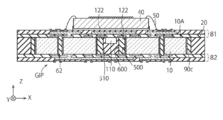
- FIG. 17 is a cross-sectional view showing a configuration example of the GIP of the fourth embodiment.
- the GIP according to the fourth embodiment has an opening 11 at the center of the glass substrate 10.
- the opening 11 is provided in the central portion of the glass substrate 10 between the first surface 10A and the second surface 10B, and has a taper on the inner side surface.
- a metal plate 120 is fitted in the opening 11.
- the metal plate 120 is provided on the back surface side of the semiconductor chip 40, absorbs the heat generated in the semiconductor chip 40, and releases the heat from the second surface 10B side of the glass substrate 10. That is, the metal plate 120 functions as a heat sink of the semiconductor chip 40.
- a highly thermally conductive material such as copper or silicon is used.
- the side surface of the metal plate 120 has a taper having an inclination substantially equal to the inner side surface of the opening 11 so as to be along the inner surface of the opening 11.
- An insulating film 65 is provided between the side surface of the metal plate 120 and the inner surface surface of the opening 11. Like the insulating films 62 and 90c, the insulating film 65 is formed by filling the resin material between the side surface of the metal plate 120 and the inner surface of the opening 11 at the same time as forming the insulating film 90a. Therefore, the insulating film 65 extends in a direction inclined with respect to the first and second surfaces 10A and 10B along the side surface of the metal plate 120 and the inner surface surface of the opening 11.
- the insulating film 65 is made of the same material as the insulating films 90a, 90c, 62, and is continuously and seamlessly connected to the insulating films 90a, 90c, 62. As a result, the insulating film 65 can sufficiently protect the end portion of the opening 11 of the glass substrate 10.
- the insulating film 65 is made of the same material as the insulating film 90b, and may be continuously and seamlessly connected. As a result, the insulating film 65 can more reliably protect the end portion of the opening 11 of the glass substrate 10. In addition, the stress on the glass substrate 10 is also reduced.
- the fourth embodiment is effective when the stress applied to the glass substrate 10 differs between the first surface 10A and the second surface 10B due to differences in the film thickness, the number of layers, the material, etc. of the laminated wiring portions 81 and 82. be.
- FIG. 18 is a cross-sectional view showing an example of a boundary portion between the opening 11 and the metal plate 120. It is assumed that the laminated wiring portion 81 is 20 ⁇ m, the laminated wiring portion 82 is 30 ⁇ m, and the insulating film 65 is 100 ⁇ m.
- the laminated wiring portions 81 and 82 each include a metal film having the same pattern and an insulating film having the same pattern, each having the same thickness.
- FIG. 19 is a graph showing the results of warpage analysis of the glass substrate 10 shown in FIG.
- the inclination angle ⁇ of the taper is the inclination angle of the inner wall surface of the opening 11 on the glass substrate 10 side with respect to the second surface 10B having the relatively thick laminated wiring portion 82.
- the warp is minimized when the inclination angle ⁇ is about 75 degrees. That is, if the inclination angle ⁇ of the taper of the opening 11 and the metal plate 120 is set to about 75 degrees, the warp applied to the glass substrate 10 is minimized.
- the side surface of the metal plate 120 and the inner side surface of the opening 11 are tapered, and the insulating film 65 is filled along the taper. Thereby, the warp generated in the glass substrate 10 can be controlled and reduced.
- the fourth embodiment may be the same as the corresponding configurations of the first embodiment. Therefore, the fourth embodiment can obtain the same effect as the first embodiment. Further, the fourth embodiment may be applied to either the second or third embodiment.
- a part of the laminated wiring portions 81 and 82 or the metal films 92a and 92b may be used as an antenna for wireless communication.
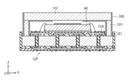
- FIG. 20 is a cross-sectional view showing an example of an application using GIP according to the above embodiment.
- the GIP may be any of the above-mentioned first to fourth embodiments or a modification thereof.
- the semiconductor chip 40 is a CMOS image sensor chip, and the light receiving surface is directed upward.
- the semiconductor chip 40 is adhered on the GIP with an adhesive, and is electrically connected to a part of the wiring of the GIP by the bonding wire 50.
- a fixed frame 101 is arranged around the semiconductor chip 40.
- the fixing frame 101 is provided to fix the cover glass 102 at a predetermined position above the light receiving surface of the semiconductor chip 40.
- the cover glass 102 protects the light receiving surface of the semiconductor chip 40 and allows incident light to pass through the light receiving surface.
- the cover glass 102 may be a condenser lens.
- the GIP according to the present embodiment can be used as a substrate of the CMOS image sensor.
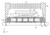
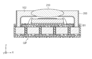
- FIG. 21 is a cross-sectional view showing another example of the application using GIP according to the above embodiment.
- the GIP is basically any of the above-mentioned first to fourth embodiments or a modification thereof.
- the CMOS image sensor chip 40, the signal processing chip 103, the power amplifier 104, and the antenna 105 are mounted on one GIP and are configured as one module. Therefore, the GIP has a relatively large size.
- the metal plate 120 is embedded in the GIP below the CMOS image sensor chip 40. Below the power amplifier 104, a metal plate 121 is embedded in the GIP.
- the arrangement of the semiconductor chip 40, the fixed frame 101, and the cover glass 102 is the same as in Application Example 1.
- a metal plate 120 is fitted in the lower portion of the opening 11. In this way, the metal plate 120 is provided in the opening 11, and the semiconductor chip 40 is provided on the metal plate 120.
- the metal plate 120 is in contact with the back surface of the semiconductor chip 40 via the wiring 83a and the metal pad 71, absorbs the heat generated in the semiconductor chip 40, and transfers the heat to the second surface 10B side of the glass substrate 10. Emit from.
- the material of the wiring 83a and the metal pad 71 is interposed between the metal plate 120 and the semiconductor chip 40. Further, materials for the wiring 83b and the metal pad 72 are provided on the second surface 10B side of the metal plate 120.
- the materials of the wirings 83a and 83b and the metal pads 71 and 72 are provided for the heat dissipation path.
- the signal processing chip 103 is provided on the second surface 10B side and is electrically connected to the electrode pad 72.
- the signal processing chip 103 performs arithmetic processing on a pixel signal that has been photoelectrically converted and AD-converted by the semiconductor chip 40.
- GIP has an opening 111 in addition to the opening 11.
- the metal plate 121 is fitted in the opening 111.
- the power amplifier 104 is provided under the metal plate 121 in order to amplify a signal or the like received by the antenna 105. In this way, the metal plate 121 is provided in the opening 111.
- the metal plate 121 is in contact with the back surface of the power amplifier 104 via the wiring 83b and the metal pad 72, absorbs the heat generated in the power amplifier 104, and transfers the heat to the first surface 10A side of the glass substrate 10. Emit from.
- the material of the wiring 83b and the metal pad 72 is interposed between the metal plate 121 and the power amplifier 104.
- the material of the wiring 83a and the metal pad 71 is provided on the first surface 10A side of the metal plate 121.
- the materials of the wirings 83a and 83b and the metal pads 71 and 72 are provided for the heat dissipation path.
- the antenna 105 is provided on the first surface 10A side of the GIP.
- the antenna 105 is provided to receive an external signal and transmit an internal signal.
- the antenna 105 is configured by providing a metal wiring 105a that functions as an antenna element on a glass substrate.
- GIP is characterized by low power loss of high frequency signals. Therefore, it is advantageous to mount, for example, an antenna for 5G as in Application Example 2.
- the GIP according to the present embodiment can also be used as the substrate of the module of the CMOS image sensor.
- the semiconductor device according to the present embodiment is advantageous in terms of space saving and low power loss.
- the insulating film Before forming the metal films 83a_1, 83b_1, 61, the insulating film may be formed in the first surface 10A, the second surface 10B, and the via V1 of the glass substrate 10.
- an insulating material such as an epoxy resin may be used.
- metal films 83a_1, 83b_1, 61 are formed on the surface of the insulating film in the first surface 10A, the second surface 10B, and the via V1 of the glass substrate 10.
- the metal films 83a_1, 83b_1, 61 are processed by using the laser processing technique.
- the glass substrate 10 is separated into pieces by the dicing process.
- the glass substrate 10 is arranged on the frame 20, and the wiring layers 81 and 82 are formed.
- the metal films 83a_1, 83b_1, 61 are formed on the insulating film without directly contacting the glass substrate 10.
- the insulating films 90a and 90b can seamlessly and continuously cover the first surface 10A, the second surface 10B, and the side surface 10C of the glass substrate 10. Therefore, the first modification can obtain the effect of the first embodiment.
- the insulating film may be formed on the metal films 83a_1, 83b_1, 61 before the dicing step.
- an insulating film is formed on the metal films 83a_1, 83b_1, 61.
- the insulating film is also embedded in the via V1 and also covers the metal film 61.
- the glass substrate 10 is fragmented by the dicing process.
- the glass substrate 10 is arranged on the frame 20, and the wiring layers 81 and 82 are formed.
- the insulating films 90a and 90b embedded between the frame 20 and the glass substrate 10 are different from the insulating films covering the metal films 83a_1, 83b_1 and 61 and are not continuous.
- the insulating films 90a and 90b can seamlessly and continuously cover the first surface 10A, the second surface 10B, and the side surface 10C of the glass substrate 10. Therefore, in the second modification, the effect of the first embodiment can be obtained.
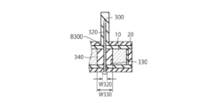
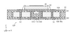
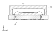
- FIG. 22 is a cross-sectional view showing a configuration example of the semiconductor device according to the fifth embodiment.
- the GIP glass substrate 10 is fastened to the housing 300 provided with the lens group 310 by screws 320 as fasteners.
- the glass substrate 10 is provided with a fastening hole 330 for passing the screw 320 through.
- the fastening hole 330 is provided so as to penetrate the glass substrate 10 between the first surface 10A and the second surface 20B.
- a filler 340 is filled between the fastening hole 330 and the screw 320.
- the screw 320 penetrates the filler 340 in the fastening hole 330 and is fastened to the housing 300 to fix the glass substrate 10 to the housing 300.
- an insulating material such as resin is used for the filler 340.
- the frame 20 is adhered to the side surface of the glass substrate 10 with an adhesive 350.
- the housing 300 has a substantially rectangular tubular shape so as to surround the semiconductor chip 40.
- a lens group 310 is provided above the semiconductor chip 40 of the housing 300. The light that has passed through the lens group 310 is incident on the semiconductor chip 40 as a CIS or the like.
- the fastening hole 330 can be formed by irradiating a laser beam to alter the glass substrate 10 and etching the altered portion with a hydrofluoric acid solution or the like. Alternatively, the fastening hole 330 may be formed by scraping the glass substrate 10 using laser ablation.
- the GIP is directly fastened to the housing 300, and the end portion of the housing 300 is arranged on the GIP and is in contact with the GIP.
- the GIP can be fastened to the housing 300 without impairing the characteristics of the glass substrate 10, such as high flatness, small warpage, and small tilt.
- the contact surface B300 between the housing 300 and the GIP serves as an optical axis reference surface between the optical axis of the lens group 310 and the optical axis of the semiconductor chip 40.
- the optical axis reference plane is a contact surface having a large influence because the optical axis of the lens group 310 and the optical axis of the semiconductor chip 40 are substantially aligned with each other.
- the optical axis of the lens group 310 and the optical axis of the semiconductor chip 40 are processed by processing the surfaces of the housing 300 and the GIP facing the contact surface B300 with high accuracy. Can be almost matched with.
- the configuration of the GIP, the fixed frame 101, the cover glass 102, and the semiconductor chip 40 may be the same as that of either the above embodiment or the above modification.
- the GIP, the semiconductor chip 40, and the lens group 310 may be configured as an integrated module.
- this module can be incorporated into a product such as a camera while keeping the optical axes of the semiconductor chip 40 and the lens group 310 substantially aligned.
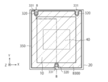
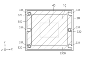
- FIG. 23 is a schematic plan view showing a configuration example of the semiconductor device according to the fifth embodiment.
- the plane layout of the fastening hole 330 will be described with reference to FIG. 23.
- FIG. 22 is a cross section taken along the line AA of FIG. 23.
- three fastening holes 330 are provided in the glass substrate 10.
- the fastening hole 330 is provided in the contact surface B300 between the housing 300 and the GIP.
- the fastening holes 330 are unevenly arranged on one side of the glass substrate 10, resonance or abnormal vibration may be induced when micro-vibration propagates to the GIP. In this case, vibration may propagate to the semiconductor chip 40 and components mounted on the GIP and cause damage.
- the plurality of fastening holes 330 are arranged so that their centers of gravity are in the semiconductor chip 40 (overlapping) in the plane layout viewed from the Z direction. By arranging the fastening holes 330 substantially evenly in this way, it is possible to suppress damage to the semiconductor chips 40 and components mounted on the GIP.
- the number of screws 320 and fastening holes 330 is not limited to three, and any number may be used as long as it is two or more. However, as described above, it is preferable that the screws 320 and the fastening holes 330 are arranged substantially evenly on the contact surface B300.
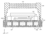
- FIG. 24 is a cross-sectional view showing a configuration example of the semiconductor device according to the sixth embodiment.
- the GIP glass substrate 10 is fastened to the mounting board 400 with screws 320, and the mounting board 400 is fastened to the housing 300 provided with the lens group 310 with screws 321 as fasteners. .. That is, the GIP is fixed to the housing 300 via the mounting board 400.
- the mounting board 400 is a wiring board in which a plurality of wiring layers 410 and a plurality of insulating layers 420 are laminated.
- a metal material such as copper is used.
- an insulating material such as a glass epoxy resin is used.
- the insulating layer 420 is provided in the region of the mounting board 400 that the housing 300 contacts, but the wiring layer 410 is not provided. As a result, the screw 321 can penetrate the mounting board 400 without contacting the wiring layer 410.
- the screw 321 penetrates the region of the insulating layer 420 of the mounting board 400 and is fastened to the housing 300.
- the configuration of the GIP itself may be the same as that of the fifth embodiment.
- the screw 320 penetrates the fastening hole 330 in the ⁇ Z direction and is fastened to the mounting substrate 400.
- the region of the mounting substrate 400 corresponding to the fastening hole 330 is also provided with the insulating layer 420, but is not provided with the wiring layer 410.
- the screws 320 can be fastened to the mounting board 400 without coming into contact with the wiring layer 410.
- the contact surface B300 between the housing 300 and the mounting substrate 400 serves as the optical axis reference surface.
- the semiconductor chip 40 mounted on the front surface of the GIP and the back surface of the GIP (that is, the front surface of the mounting substrate 400) are in a state where the parallelism is maintained. .. Therefore, by processing the surfaces of the housing 300 and the mounting substrate 400 facing the contact surface B300 with high accuracy, the optical axis of the lens group 310 and the optical axis of the semiconductor chip 40 can be substantially aligned with each other.
- the configuration of the GIP, the fixed frame 101, the cover glass 102, and the semiconductor chip 40 may be the same as that of either the above embodiment or the above modification.
- the GIP, the semiconductor chip 40, and the lens group 310 may be configured as an integrated module.
- this module can be incorporated into a product such as a camera while keeping the optical axes of the semiconductor chip 40 and the lens group 310 substantially aligned.
- FIG. 25 is a cross-sectional view showing a fastening portion of the fifth embodiment.
- the fastening hole 330 is provided on the contact surface B330 between the housing 300 and the GIP. Further, the width W330 of the fastening hole 330 is preferably larger than the width W320 of the head of the screw 320. That is, as shown in FIGS. 23 and 25, the fastening hole 330 is formed larger than the outer edge of the head of the screw 320 in a plan view seen from the Z direction (the fastening direction of the screw 320). As a result, the glass substrate 10 does not exist directly under the head of the screw 320, and the head of the screw 320 presses the filler 340 but does not directly press the glass substrate 10 at the time of fastening. As a result, it is possible to prevent the glass substrate 10 from being damaged by the load caused by fastening the screws 320. It is preferable that the relationship between the fastening hole 330 and the screw 320 of the sixth embodiment is the same.
- FIG. 26 is a cross-sectional view showing a configuration example of the semiconductor device according to the seventh embodiment.
- FIG. 27 is a schematic plan view showing a configuration example of the semiconductor device according to the seventh embodiment.
- FIG. 26 shows a cross section along line BB of FIG. 27.
- the fastening hole 330 is connected to the outside on the side surface of the glass substrate 10, and serves as a notch portion 331 for fastening.
- the notch portion 331 is a region recessed from the side surface of the glass substrate 10 toward the inside in the XY plane.
- a frame 20 is provided inside the recess of the notch 331.
- the frame 20 and the glass substrate 10 are adhered to each other by an adhesive 350.
- the screw 320 penetrates the frame 20 in the notch 331 and is fastened to the housing 300.
- the notch portion 331 may be formed in this way.
- the cutout portion 331 preferably has a smoothly continuous outer edge without having a corner, as shown in FIG. 27.
- the strength of the notch portion 331 can be maintained.
- the number of notch portions 331 is not limited to three, and may be any number of two or more. However, considering the strength of the glass substrate 10, it is preferable to reduce the number of notches 331 as much as possible and make the contact portion with the frame 20 as small as possible.
- the notch portions 331 are preferably arranged substantially evenly on the contact surface B300 between the GIP and the housing 300. Even with such a notch portion 331, the effect of the present disclosure is not lost.
- the fastening hole 330 and the notch 331 may be mixed.
- FIG. 28 is a cross-sectional view showing a configuration example of a semiconductor device according to a modified example of the seventh embodiment.
- the six notches 331 are arranged line-symmetrically or point-symmetrically with respect to the center line or the center of the glass substrate 10.
- the notch portion 331 can be provided without impairing the characteristics such as the flatness of the glass substrate 10.
- the screws 320 are fastened to the three notch portions 331 out of the six notch portions 331.
- the size of the notch 331 of the glass substrate 10 is preferably the same, but the size may be changed as necessary in consideration of the overall balance.
- the seventh embodiment and the present modification may be applied to the sixth embodiment.
- FIG. 29 is a cross-sectional view showing a configuration example of the semiconductor device according to the eighth embodiment.
- FIG. 30 is a plan view showing a configuration example of the semiconductor device according to the eighth embodiment.
- the frame 25 is provided between the side surface of the glass substrate 10 and the frame 20.
- the frame 25 as the second frame is provided directly below the housing 300, and is provided for fastening the GIP to the housing 300 with screws 320.
- a material other than glass is used for the frame 25.
- a metal material such as stainless steel is used when high rigidity is required, an aluminum alloy or titanium alloy is used when weight reduction is required, and a copper alloy or the like is used when high thermal conductivity is required. Is used.
- a fastening hole 330 through which the screw 320 is passed is provided in the frame 25.
- three fastening holes 330 are provided in the frame 25, but the number of fastening holes 330 is not limited. Further, it is preferable that the fastening holes 330 are arranged substantially evenly in the frame 25.
- the frame 25 is adhered to the side surface of the glass substrate 10 with an adhesive 350.
- the frame 20 is similarly adhered to the outer surface of the frame 25 with an adhesive 350.
- the frame 25 is configured as a part of the GIP, consideration must be given to bring the coefficient of linear expansion and the like closer to the glass substrate 10.
- the relationship between the linear expansion coefficients of the glass substrate 10, the frame 25, and the housing 300 is preferably glass substrate 10 ⁇ frame 25 ⁇ housing 300, or housing 300 ⁇ frame 25 ⁇ glass substrate 10.
- the coefficient of thermal expansion at the fastening portion from the glass substrate 10 to the housing 300 is configured to gradually change, so that the stress of the entire module is reduced.
- the frame 25 may also have a function of protecting the side surface of the glass substrate 10. In this case, the frame 20 may be omitted. However, this package is made into individual pieces through a dicing step of cutting the resin frame 20 in the manufacturing process. Therefore, when the frame 25 is made of a metal material or the like that cannot be diced, it is preferable that the frame 20 is provided in addition to the frame 25.
- FIG. 31 is a cross-sectional view showing a configuration example of a semiconductor device according to a modified example of the eighth embodiment.
- a heat radiating portion 360 that is fastened and contacts with a screw 320 is provided at the bottom of the GIP.
- the heat radiating portion 360 is fastened to the second surface 10B side of the glass substrate 10 by screws 320.
- the screw 320 fastens the heat radiating portion 360 to the GIP together with the fastening of the GIP and the housing 300.
- a material such as copper or aluminum is used as a material having high thermal conductivity.
- the heat of the housing 300 and the GIP can be exhausted from the heat radiating unit 360 via the screws 320 and the like.
- the heat of the GIP is transferred to the heat radiating unit 360 via the laminated wiring portions 81 and 82, and can be efficiently exhausted from the heat radiating unit 360.
- FIG. 32 is a cross-sectional view showing a configuration example of the semiconductor device according to the ninth embodiment.
- the GIP glass substrate 10 is fastened to the substrate 401 with screws 320, and the substrate 401 is fastened to the housing 300 including the lens group 310 with screws 321. That is, the GIP is fixed to the housing 300 via the substrate 401.
- the substrate 401 is a plate-shaped substrate having excellent heat dissipation, flatness, parallelism, and rigidity.
- the substrate 401 for example, copper, aluminum, tungsten, molybdenum, niobium, titanium, alloys containing these metals, and alloys such as stainless steel, duralumin, Invar, Kovar, and brass are used.
- the glass substrate 10 is fastened to the substrate 401 with screws 320 via the frame 25 and comes into close contact with the substrate 401.
- the substrate 401 is fastened to the housing 300 via the screws 321 and is brought into close contact with the housing 300, so that the rigidity and heat dissipation can be further improved.
- the screw 321 penetrates the substrate 401 and is fastened to the housing 300.
- the configuration of the GIP itself may be the same as that of the eighth embodiment.
- the screw 320 penetrates the frame 25 in the ⁇ Z direction and is fastened to the substrate 401.
- the substrate 401 and GIP may be fixed via an adhesive or the like having a high thermal conductivity.
- FIG. 33 is a cross-sectional view showing a configuration example of the semiconductor device according to the tenth embodiment.
- FIG. 34 is a schematic plan view showing a configuration example of the semiconductor device according to the tenth embodiment.
- the electronic component 110 is built in the glass substrate 10 of the GIP.
- a through hole (cavity) 500 is provided directly below the semiconductor chip 40 of the glass substrate 10, and the electronic component 110 is arranged in the through hole 500.
- the through hole 500 is provided at the center of the glass substrate 10 so as to penetrate the glass substrate 10 between the first surface 10A and the second surface 20B.
- the through hole 500 is formed to have a size capable of accommodating the electronic component 110.
- the space of the through hole 500 other than the electronic component 110 is filled with the insulating film 510.
- the insulating film 510 may be made of the same material as the insulating films 62 and 90c, and may be embedded in the space of the through hole 500 in the same process as the formation of the insulating films 62 and 90c.
- the through hole 500 can be formed by irradiating a laser beam to alter the glass substrate 10 and etching the altered portion with a hydrofluoric acid solution or the like.
- the through hole 500 may be formed by scraping the glass substrate 10 using laser ablation.
- the upper surface of the electronic component 110 is aligned with the first surface 10A of the glass substrate 10. Further, the electronic component 110 is connected to any of the wirings of the laminated wiring portion 81 on the first surface 10A side of the glass substrate 10. As a result, electric power can be supplied to the electronic component 110 from the outside via the wiring of the laminated wiring portion 81, a control signal can be given to the electronic component 110, or data can be output from the electronic component 110.
- Other configurations of the GIP of the tenth embodiment may be similar to the corresponding configurations of any of the above embodiments or modifications. In the tenth embodiment, the presence or absence of the frame 20 does not matter.
- the electronic component 110 may be, for example, either an active component or a passive component.
- the electronic component 110 is, for example, as an active component, DSP (Digital Signal Processor), DRAM (Dynamic Random Access Memory), SRAM (Static RAM), MRAM (Magnetoresistive RAM), FPGA (Field-Programmable Gate Array) gyro sensor, acceleration.
- a sensor, an inertial measurement unit (IMU (Inertial Measurement Unit)), etc. may be used.
- the electronic component 110 may be, for example, a chip capacitor, a chip inductor, a thin film capacitor, or the like as a passive component.
- the wiring distance between the electronic component 110 and the semiconductor chip 40 is shortened. This speeds up the operation of the entire package and reduces noise. For example, when the semiconductor chip 40 or the electronic component 110 includes a capacitor, the noise of the capacitor is reduced. When the semiconductor chip 40 or the electronic component 110 includes a CPU, the operation of the CPU is speeded up. When the semiconductor chip 40 or the electronic component 110 includes an IMU, the detection accuracy of the IMU is improved.
- the electronic component 110 is arranged in the glass substrate 10, the size of the package is reduced.
- the degree of freedom is high when installing a heat sink or the like on the GIP.
- the module manufacturing method according to the tenth embodiment is as follows. The process shown in FIGS. 8 to 12 is performed. At this time, the glass substrate 10 and the frame 20 are mounted on the support substrate (support tape) 502. Further, a through hole 500 is formed in the central portion of the glass substrate 10.
- FIG. 35 is a cross-sectional view showing a method of manufacturing a semiconductor device according to the tenth embodiment.
- the first surface 10A of the glass substrate 10 is arranged toward the support substrate 502 side. Therefore, at this stage, the surface of the electronic component 110 is substantially flush with the first surface 10A of the glass substrate 10.
- the resin material described with reference to FIG. 13 embeds the via V1 and the like, and also embeds the inside of the through hole 500. That is, the insulating film 510 is formed at the same time as the insulating films 62 and 90c.
- the electronic component 110 is resin-sealed with the insulating film 510 while its surface is aligned with the first surface 10A of the glass substrate 10.
- the laminated wiring portion 81 formed thereafter can easily connect the terminal of the electronic component 110 and the wiring on the first surface 10A of the glass substrate 10.
- the module according to the tenth embodiment is completed through the steps described with reference to FIGS. 13 to 15 or 16.
- FIG. 36 is a cross-sectional view showing a configuration example of a semiconductor device according to a modified example of the tenth embodiment.
- one surface of the electronic component 110 is aligned with the second surface 10B of the glass substrate 10. Further, the electronic component 110 is connected to any of the wirings of the laminated wiring portion 82 on the second surface 10B side of the glass substrate 10.
- Other configurations of this modification may be the same as the corresponding configurations of the tenth embodiment. Therefore, this modification can obtain the same effect as that of the tenth embodiment.
- the direction of the glass substrate 10 shown in FIG. 35 may be turned upside down, and the second surface 10B may be manufactured toward the support substrate 502.
- the bottom surface of the electronic component 110 is substantially flush with the second surface 10B of the glass substrate 10.
- the laminated wiring portion 82 formed thereafter can easily connect the terminal of the electronic component 110 and the wiring on the second surface 10B of the glass substrate 10.
- FIG. 37 is a cross-sectional view showing a configuration example of the semiconductor device according to the eleventh embodiment.
- the plan view of the eleventh embodiment may be the same as that of FIG. 34.
- a counterbore (recess) 501 is provided directly below the semiconductor chip 40 of the glass substrate 10, and the electronic component 110 is arranged in the counterbore 501.
- the counterbore 501 is provided on the first surface 10A of the glass substrate 10, does not penetrate the glass substrate 10, and has a bottom.
- the counterbore 501 is formed in a size that can accommodate the electronic component 110.
- the space inside the counterbore 501 other than the electronic component 110 is filled with the insulating film 510.
- the counterbore 501 can be formed by irradiating a laser beam to alter the glass substrate 10 and etching the altered portion with a hydrofluoric acid solution or the like.
- the counterbore 501 may be formed by scraping the glass substrate 10 using laser ablation.
- the upper surface of the electronic component 110 is aligned with the first surface 10A of the glass substrate 10. Further, the electronic component 110 is connected to any of the wirings of the laminated wiring portion 81 on the first surface 10A side of the glass substrate 10.
- Other configurations of the GIP of the eleventh embodiment may be similar to the corresponding configurations of the tenth embodiment. Therefore, the eleventh embodiment can obtain the same effect as the tenth embodiment.
- the module manufacturing method according to the eleventh embodiment is as follows. The process shown in FIGS. 8 to 12 is performed. At this time, the glass substrate 10 and the frame 20 are mounted on the support substrate (support tape) 502. Further, a counterbore 501 is formed in the central portion of the glass substrate 10. As shown in FIG. 38, the glass substrate 10 is arranged on the support substrate 502 with the counterbore 501 facing upward.
- FIG. 38 is a cross-sectional view showing a method of manufacturing a semiconductor device according to the eleventh embodiment.
- the electronic component 110 is mounted and adhered to the counterbore 501.
- the counterbore 501 is formed so that the surface of the electronic component 110 is substantially flush with the first surface 10A of the glass substrate 10.
- the resin material described with reference to FIG. 13 embeds the via V1 and the like, and also embeds the inside of the counterbore 501.
- the electronic component 110 is resin-sealed with its surface aligned with the first surface 10A of the glass substrate 10. As a result, the laminated wiring portion 81 formed thereafter can easily connect the terminal of the electronic component 110 and the wiring on the first surface 10A of the glass substrate 10.
- FIG. 39 is a cross-sectional view showing a configuration example of the semiconductor device according to the twelfth embodiment.
- FIG. 40 is a plan view showing a configuration example of the semiconductor device according to the twelfth embodiment.
- a plurality of electronic components 110 are built in the through holes 500 of the glass substrate 10. By changing the size of the through hole 500 in this way, a plurality of electronic components 110 may be incorporated in the through hole 500.
- the upper surfaces of the plurality of components 110 can be formed on the glass substrate 10 by manufacturing in the same manner as in the tenth embodiment. It can be almost flush with the first surface 10A (or the second surface 10B). As a result, a plurality of electronic components 110 having different areas and heights (thicknesses) can be arranged in the through hole 500 and connected to the laminated wiring portion 81 (or 82).
- twelfth embodiment may be the same as the corresponding configurations of the tenth embodiment. Thereby, the twelfth embodiment can obtain the same effect as the tenth embodiment.
- FIG. 41 is a cross-sectional view showing a configuration example of the semiconductor device according to the thirteenth embodiment.
- the plan view of the thirteenth embodiment may be the same as that of FIG. 40.
- a plurality of counterbore 501s are provided directly below the semiconductor chip 40 of the glass substrate 10, and a plurality of electronic components 110 are arranged in individual counterbore 501s. By providing the plurality of counterbore 501s in this way, the plurality of electronic components 110 may be incorporated in the glass substrate 10.
- the depths of the plurality of counterbore 501s are set according to the thickness of each electronic component 110. It is preferable to do so. As a result, the upper surfaces of the plurality of components 110 can be aligned substantially flush with the first surface 10A of the glass substrate 10.
- the electronic component 110 when the electronic component 110 is a gyro sensor, it is preferable that the electronic component 110 is arranged directly under the semiconductor chip 40 along the central axis of the semiconductor chip 40. This improves the detection accuracy of the angular velocity of the gyro sensor.
- a moving object such as a drone or a car may vibrate at several hundred Hz.
- the output signal (particularly, angular velocity) from the gyro sensor as the electronic component 110 needs to be corrected at several hundred Hz, and high-precision correction processing is required.
- NS By arranging the electronic component 110 directly below the semiconductor chip 40 so as to align with its central axis as in the present disclosure, correction processing such as angular velocity becomes relatively easy.
- the gyro sensor when the gyro sensor is arranged at a position deviated from the central axis of the semiconductor chip 40, it is necessary to arrange a plurality of gyro sensors around the semiconductor chip 40. However, the number of gyro sensors can be reduced by arranging the electronic component 110 directly below the semiconductor chip 40 along the central axis as described in the present disclosure.
- FIG. 42 is a cross-sectional view showing a configuration example of the semiconductor device according to the 14th embodiment.
- FIG. 43 is a schematic plan view showing a configuration example of the semiconductor device according to the 14th embodiment.
- the electronic component 110 is built in the frame 20 of the GIP.
- the frame 20 is provided with a through hole (cavity) 500, and the electronic component 110 is arranged in the through hole 500.
- the through hole 500 is provided so as to penetrate between the third surface 20A and the fourth surface 20B of the frame 20.
- the through hole 500 is formed in a size that can accommodate the electronic component 110.
- the space of the through hole 500 other than the electronic component 110 is filled with the insulating film 510.
- the insulating film 510 may be made of the same material as the insulating films 62 and 90c, and may be embedded in the space of the through hole 500 in the same process as the formation of the insulating films 62 and 90c.
- the through hole 500 may be formed by cutting the frame 20 using laser ablation.
- the upper surface of the electronic component 110 is aligned with the third surface 20A of the frame 20. Further, the electronic component 110 is connected to any of the wirings of the laminated wiring portion 81 on the third surface 20A side of the frame 20. As a result, electric power can be supplied to the electronic component 110 from the outside via the wiring of the laminated wiring section 81 to give a control signal to the electronic component 110, or data can be output from the electronic component 110.
- Other configurations of the 14th embodiment may be the same as the corresponding configurations of the 10th embodiment.
- the electronic component 110 is not provided directly under the semiconductor chip 40, the size of the package can be reduced. In addition, there is a high degree of freedom in the installation of heat sinks and the like.
- the frame 20 having the through hole 500 is mounted on the support substrate 502, and the electronic component 110 is mounted on the support substrate 502 in the through hole 500. Subsequent steps may be the same as the manufacturing steps of the tenth embodiment.
- FIG. 44 is a cross-sectional view showing a configuration example of a semiconductor device according to a modified example of the 14th embodiment.
- one surface of the electronic component 110 is aligned with the fourth surface 20B of the frame 20. Further, the electronic component 110 is connected to any of the wirings of the laminated wiring portion 82 on the fourth surface 20B side of the frame 20.
- Other configurations of this modification may be the same as the corresponding configurations of the 14th embodiment. Therefore, this modification can obtain the same effect as that of the 14th embodiment.
- FIG. 45 is a cross-sectional view showing a configuration example of the semiconductor device according to the fifteenth embodiment.
- the plan view of the fifteenth embodiment may be the same as that of FIG. 43.
- the frame 20 is provided with a counterbore (recess) 501, and the electronic component 110 is arranged in the counterbore 501.
- the counterbore 501 is provided on the third surface 20A of the frame 20, does not penetrate the frame 20, and has a bottom.
- the counterbore 501 is formed in a size that can accommodate the electronic component 110.
- the space inside the counterbore 501 other than the electronic component 110 is filled with the insulating film 510.
- the counterbore 501 may be formed by scraping the frame 20 using laser ablation.
- the upper surface of the electronic component 110 is aligned with the third surface 20A of the frame 20. Further, the electronic component 110 is connected to any of the wirings of the laminated wiring portion 81 on the third surface 20A side of the frame 20.
- Other configurations of the GIP of the fifteenth embodiment may be similar to the corresponding configurations of the fourteenth embodiment. Therefore, the fifteenth embodiment can obtain the same effect as the fourteenth embodiment.
- the frame 20 having the counterbore 501 is mounted on the support substrate 502, and the electronic component 110 is mounted in the counterbore 501.
- Other steps may be the same as the manufacturing steps of the 14th embodiment.
- FIG. 46 is a cross-sectional view showing a configuration example of the semiconductor device according to the 16th embodiment.
- FIG. 47 is a plan view showing a configuration example of the semiconductor device according to the 16th embodiment.
- a plurality of electronic components 110 are built in the through hole 500 of the frame 20. By changing the size of the through hole 500 in this way, a plurality of electronic components 110 may be incorporated in the through hole 500.
- the upper surfaces of the plurality of components 110 can be formed on the upper surface of the frame 20 by manufacturing in the same manner as in the 14th embodiment. It can be almost flush with the three surfaces 20A (or the fourth surface 20B). As a result, a plurality of electronic components 110 having different areas or heights (thicknesses) can be arranged in the through hole 500 and connected to the laminated wiring portion 81 (or 82).
- the 16th embodiment may be combined with the 15th embodiment.
- a plurality of electronic components 110 having different heights or areas can be incorporated in the counterbore 501 of the frame 20.
- FIG. 48 is a cross-sectional view showing a configuration example of the semiconductor device according to the 17th embodiment.
- FIG. 49 is a plan view showing a configuration example of the semiconductor device according to the 17th embodiment.
- the heat radiating member 122 is built in the through hole 500 of the glass substrate 10, and the electronic component 110 is built in the through hole (second through hole) 600 provided in the heat radiating member 122. There is.
- the heat radiating member 122 is formed in a size that can be accommodated in the through hole 500, and is provided with a through hole 600 so that the electronic component 110 can be accommodated.
- the outer edge of the heat radiating member 122 When viewed from the Z direction, the outer edge of the heat radiating member 122 has a shape substantially similar to, for example, the through hole 500, and is smaller than the through hole 500, as shown in FIG. 49.
- the through hole 600 of the heat radiating member 122 has a shape substantially similar to that of the electronic component 110, and is larger than that of the electronic component 110. Therefore, the heat radiating member 122 is formed into a frame shape when viewed from the Z direction.
- the height (thickness) of the heat radiating member 122 in the Z direction may be substantially the same as the height (thickness) of the glass substrate 10 or may be slightly lower (thinner).
- a highly thermally conductive material such as copper or silicon is used.
- the through hole 600 of the heat radiating member 122 may be formed by using a lithography technique and an etching technique. Alternatively, the through hole 600 of the heat radiating member 122 may be formed by scraping the heat radiating member 122 by using laser ablation.
- a frame 20 having a through hole 500 is mounted on a support substrate 502, and a heat radiating member 122 having a through hole 600 is mounted on a support substrate 502 in the through hole 500. Further, the electronic component 110 is mounted on the support substrate 502 in the through hole 600. Subsequent steps may be the same as the manufacturing steps of the tenth embodiment.
- the heat radiating member 122 can quickly transfer the heat of the semiconductor chip 40 and the electronic component 110 to the second surface 10B side of the glass substrate 10 and exhaust the heat. Further, when the heat radiating member 122 is made of silicon, the difference in the selective expansion coefficient between the heat radiating member 122 and the glass substrate 10 is small. As a result, warpage of the package is suppressed, leading to improvement in reliability.
- the frame 20 may be omitted.
- FIG. 50 is a cross-sectional view showing a configuration example of the semiconductor device according to the eighteenth embodiment.
- the plan view of the eighteenth embodiment may be the same as that of FIG. 49.
- the heat radiating member 122 is provided with a counterbore (recess) 601 and the electronic component 110 is arranged in the counterbore (second counterbore) 601.
- the counterbore 601 does not penetrate the heat radiating member 122 and has a bottom.
- the counterbore 601 is formed in a size that can accommodate the electronic component 110.
- the space inside the counterbore 601 other than the electronic component 110 is filled with the insulating film 510.
- the counterbore 601 may be formed by a lithography technique and an etching technique, or may be formed by using laser ablation.
- the 18th embodiment may be the same as the corresponding configurations of the 17th embodiment. Therefore, the 18th embodiment can obtain the same effect as the 17th embodiment. Further, according to the eighteenth embodiment, the heat radiating member 122 is provided so as to cover the side portion and the bottom portion of the electronic component 110. Therefore, the heat dissipation function of the heat dissipation member 122 is improved. In the 18th embodiment, the frame 20 may be omitted.
- a plurality of electronic components 110 may be provided in the through hole 600 or the counterbore 601.
- FIG. 51 is a cross-sectional view showing an example of the semiconductor device according to the 19th embodiment.
- the GIP may be either the above embodiment or a modification thereof.
- the fixed frame 101 is made of glass.
- the fixed frame (glass frame) 101 is provided so as to surround the semiconductor chip 40, and has a substantially rectangular cylindrical shape. Further, a part of the insulating films 85a and 90a on the first surface 10A of the glass substrate 10 has been removed, and one end of the fixed frame 101 is directly connected to the first surface 10A of the glass substrate 10.
- glass of the same type as the glass substrate 10 or a glass material having a linear expansion coefficient close to that is used.
- the cover glass 102 is connected to the other end of the fixed frame 101 and is provided so as to cover the upper side of the semiconductor chip 40.
- the cover glass 102 for example, a glass of the same type as the glass substrate 10 or a glass material having a linear expansion coefficient close to that is used. It is preferable that the same material is used for the fixed frame 101 and the cover glass 102.
- the fixed frame 101 and the glass substrate 10 are significantly different, even if the linear expansion coefficients of the semiconductor chip 40 and the glass substrate 10 are brought close to each other to reduce the warp, the fixed frame 101 and the glass substrate 10 are used. Due to the difference in the coefficient of linear expansion line from 10, the entire package is warped.
- the fixed frame 101 is made of a glass material having the same or close to the coefficient of linear expansion of the glass substrate 10. Thereby, the warp of the package due to the fixed frame 101 can be suppressed.
- a light-shielding film 200 is provided on a part of the surfaces of the fixed frame 101 and the cover glass 102.
- the light-shielding film 200 is provided to block unnecessary light in the semiconductor chip 40 such as CIS.
- the forming region of the light-shielding film 200 may be arbitrarily set according to the purpose.
- a material having a low surface reflectance such as a light-shielding metal material such as chromium or a light-shielding resin, is used.
- the fixed frame 101 and the cover glass 102 are formed as follows. First, a flat plate-shaped substantially quadrangular glass substrate is prepared, and the central region of the glass substrate is irradiated with laser light to change the quality of the glass substrate. By etching the altered portion with a hydrofluoric acid solution or the like, the central region is hollowed out and penetrated to form a frame-shaped fixed frame 101. Alternatively, laser ablation may be used to scrape the glass substrate.
- the fixed frame 101 is adhered to the cover glass 102 using an adhesive or the like.
- a protective film is attached to the surface of the fixed frame 101 and the cover glass 102 where the light-shielding film 200 is not provided. Then, the light-shielding film 200 is vapor-deposited on the surfaces of the fixed frame 101 and the cover glass 102. By peeling the protective film from the fixed frame 101 and the cover glass 102, the light-shielding film 200 deposited on the protective film is removed together with the protective film. As a result, the light-shielding film 200 is formed in the desired regions of the fixed frame 101 and the cover glass 102.
- a part of the insulating films 85a and 90a of the GIP on which the semiconductor chip 40 is mounted is trimmed by laser light or the like.
- the outer end portion of the glass substrate 10 corresponding to the end portion of the fixed frame 101 is exposed from the insulating films 85a and 90a (wiring layer 81).
- the end of the fixed frame 101 is directly bonded to the glass substrate 10.
- an adhesive may be used, or an adhesive method such as frit glass or chemical bond may be used.
- the fixed frame 101 may be adhered to the insulating films 85a and 90a (wiring layer 81) without trimming the glass substrate 10.
- FIG. 52 is a cross-sectional view showing an example of the semiconductor device according to the twentieth embodiment.
- the 20th embodiment is different from the 19th embodiment in that the fixed frame 101 and the cover glass 102 are integrally formed of the same material.
- adhesion between the fixed frame 101 and the cover glass 102 becomes unnecessary, and the number of parts can be reduced.
- Other configurations of the 20th embodiment may be the same as the corresponding configurations of the 19th embodiment. Therefore, the 20th embodiment can obtain the same effect as the 19th embodiment.
- the cover glass 102 since the fixed frame 101 and the cover glass 102 are integrally formed, they are simply referred to as the cover glass 102.
- the cover glass 102 is formed as follows. First, a flat plate-shaped substantially quadrangular glass substrate is prepared, and the central region of the glass substrate is irradiated with laser light to change the quality of the glass substrate. At this time, the intensity of the laser beam is adjusted so as to change the quality to the middle of the thickness of the glass substrate. Next, the central region is hollowed out by etching the altered portion of the glass substrate with a hydrofluoric acid solution or the like to form a countersunk cover glass 102. At this time, the central region of the cover glass 102 is hollowed out in a concave shape but does not penetrate. Alternatively, laser ablation may be used to scrape the glass substrate.
- a protective film is attached to a region of the surface of the cover glass 102 where the light-shielding film 200 is not provided. Then, the light-shielding film 200 is vapor-deposited on the surface of the cover glass 102. By peeling the protective film from the fixed frame 101 and the cover glass 102, the light-shielding film 200 deposited on the protective film is removed together with the protective film. As a result, the light-shielding film 200 is formed in the desired regions of the fixed frame 101 and the cover glass 102. After that, the cover glass 102 is adhered to the glass substrate 10 in the same manner as in the 19th embodiment.
- FIG. 53 is a cross-sectional view showing a configuration example of a semiconductor device according to a modified example of the twentieth embodiment.
- This modification is different from the 20th embodiment in that the lens 210 is integrally formed on the cover glass 102 with the same material.
- the fixed frame, the cover glass 102, and the lens 210 can be formed at the same time, and the manufacturing cost can be reduced, the number of parts can be reduced, and the module size can be reduced.
- Other configurations of this modification may be the same as the corresponding configurations of the twentieth embodiment. Therefore, this modification can obtain the same effect as that of the 20th embodiment.
- the modified example may be combined with the 19th embodiment.
- FIG. 54 is a cross-sectional view showing a configuration example of a semiconductor device according to another modification of the 20th embodiment.
- the wiring layers directly provided on the first surface 10A and the second surface 10B of the glass substrate 10 are maintained, but most of the other laminated wiring portions 81 and 82 are omitted. Also, the frame 20 is omitted.
- the insulating films 85a, 85b, 90a, 90b are not provided on the glass substrate 10, most of the packages are made of a material having a coefficient of linear expansion of the same or close to the same. Therefore, the warp or deformation of the package due to temperature change or the like is small. Further, glass has a lower dielectric constant than the insulating films 85a, 85b, 90a and 90b such as resin. Therefore, the power loss in the package in this modification is small.
- this modification may be the same as the corresponding configurations of the 20th embodiment. Therefore, this modification can obtain the same effect as that of the twentieth embodiment.
- This modification may be combined with the 19th embodiment.
- FIG. 55 is a diagram showing an example in which the embodiment according to the present technology is used as a CMOS image sensor.
- the imaging device of the above embodiment can be used in various cases of sensing light such as visible light, infrared light, ultraviolet light, and X-ray, as shown below. That is, as shown in FIG. 55, for example, the field of appreciation for taking an image used for appreciation, the field of transportation, the field of home appliances, the field of medical / healthcare, the field of security, the field of beauty, and sports.
- the above-described embodiment can be used for an apparatus used in the field of agriculture, the field of agriculture, and the like.
- the above embodiment is used for a device for capturing an image to be used for appreciation, such as a digital camera, a smartphone, or a mobile phone having a camera function. Can be done.
- in-vehicle sensors that photograph the front, rear, surroundings, inside of a vehicle, etc., and monitor traveling vehicles and roads for safe driving such as automatic stop and recognition of the driver's condition.
- a device used for traffic such as a monitoring camera for driving, a distance measuring sensor for measuring distance between vehicles, and the like.
- a device used for home appliances such as a television receiver, a refrigerator, and an air conditioner in order to photograph a user's gesture and operate the device according to the gesture.
- a device used for home appliances such as a television receiver, a refrigerator, and an air conditioner in order to photograph a user's gesture and operate the device according to the gesture.
- the above embodiment is used for devices used for medical / healthcare, such as an endoscope and a device for performing angiography by receiving infrared light. Can be done.
- the above-described embodiment can be used for devices used for security, such as surveillance cameras for crime prevention and cameras for personal authentication.
- the above-described embodiment can be used for devices used for cosmetology, such as a skin measuring device for photographing the skin and a microscope for photographing the scalp.
- the above embodiment can be used for a device used for sports such as an action camera or a wearable camera for sports applications.
- the above embodiment can be used for devices used for agriculture, such as a camera for monitoring the condition of fields and crops.
- This technology can be applied to various other products.
- the embodiment according to the present technology is not limited to the above embodiment, and various changes can be made without departing from the gist of the present technology. Further, the effects described in the present specification are merely examples and are not limited, and other effects may be obtained.
- the present technology can have the following configurations.
- a glass substrate including a first surface, a second surface opposite the first surface, and a first surface between the first surface and the second surface. Wiring provided on the first and second surfaces and The first insulating film that covers the first surface and A second insulating film that covers the second surface and A semiconductor device comprising the first side surface and a third insulating film continuous with at least one of the first and second insulating films.
- the semiconductor device according to any one of (1) to (5), wherein the fourth insulating film is made of the same material as the first and second insulating films and is continuous. (7) The semiconductor device according to (4) or (6), wherein a part of the wiring that is in direct contact with the glass substrate is opened on the through hole. (8) The semiconductor device according to any one of (1) to (7), wherein the side surface of the third insulating film is flat. (9) The semiconductor device according to any one of (1) to (8), further comprising a frame provided on the first side surface outside the third insulating film. (10) The frame has a third surface on the first surface side, a fourth surface on the second surface side, and a second surface facing the first side surface.
- the first insulating film is continuously provided from the first surface to the third surface.
- (11) A second metal film provided on the third surface of the frame and The semiconductor device according to claim 10, further comprising a third metal film provided on the fourth surface of the frame.
- (12) The semiconductor device according to any one of (9) to (11), wherein the frame is made of a material having a coefficient of linear expansion substantially equal to the coefficient of linear expansion of the glass substrate.
- the first side surface of the glass substrate has a curved surface shape protruding outward in a cross section in a direction perpendicular to the first surface.
- the first side surface of the glass substrate has a curved surface shape that protrudes outward in a cross section in a direction perpendicular to the first surface.
- the inner surface of the through hole also has a curved surface shape that protrudes inward of the through hole in a cross section in a direction perpendicular to the first surface.
- the semiconductor device according to (6), wherein the curvature of the first side surface is substantially equal to the curvature of the inner surface of the through hole.
- the semiconductor device according to item 1 (16) The semiconductor device according to (15), wherein the inner wall surface of the second through hole and the side surface of the metal plate are inclined with respect to the first surface or the second surface. (17) The semiconductor device according to any one of (1) to (16), further comprising an alignment mark provided on the first surface of the glass substrate. (18) The semiconductor device according to (11), wherein the second and third metal films are used as an antenna for wireless communication. (19) The semiconductor device according to any one of (1) to (18), wherein an antenna is mounted on the first surface of the glass substrate. (20) The semiconductor device according to any one of (1) to (18), wherein a semiconductor chip is mounted on the first surface of the glass substrate. (21) The semiconductor device according to (20), wherein the semiconductor chip is an image sensor chip.
- the first surface, the second surface on the opposite side of the first surface, and the first surface between the first surface and the second surface are included, and the first surface and the second surface A glass substrate with fastening holes that penetrate between them, Wiring layers provided on the first and second surfaces and A semiconductor chip provided above the glass substrate and A housing provided around the semiconductor chip and With the lens provided in the housing A semiconductor device including a fastener for fastening the glass substrate and the housing through the fastening hole.
- a plurality of the fastening holes are provided in the glass substrate, and the fastening holes are provided in the glass substrate.
- the fastener is any one of (22) to (25) that fastens the housing and the glass substrate so that the optical axis of the lens and the optical axis of the semiconductor chip substantially coincide with each other.
- the semiconductor device according to the section. The glass substrate has a through hole penetrating between the first surface and the second surface.
- the semiconductor device according to any one of (1) to (21), which is provided in the through hole, is connected to any of the wirings, and further includes an electronic component.
- the frame has a through hole penetrating between the third surface and the fourth surface.
- the semiconductor device according to any one of (9) to (12), which is provided in the through hole is connected to any of the wirings, and further includes an electronic component.
- the glass substrate has a counterbore provided on the first surface and has a counterbore.
- the semiconductor device according to any one of (1) to (21), which is provided in the counterbore, is connected to any of the wirings, and further includes an electronic component.
- the frame has a counterbore provided on the third surface.
- the semiconductor device according to any one of (9) to (12), which is provided in the counterbore, is connected to any of the wirings, and further includes an electronic component.
- a plurality of the electronic components having different thicknesses are provided in the through hole.
- a plurality of the electronic components having different thicknesses are provided in each of the plurality of counterbores having different depths.
- a plurality of the electronic components having different thicknesses are provided in each of the plurality of counterbores having different depths.
- the glass substrate has a through hole penetrating between the first surface and the second surface. A heat radiating member provided in the through hole and having a second through hole is further provided.
- the semiconductor device according to (41), wherein the glass frame and the cover glass are made of the same material as the glass substrate.
Landscapes
- Solid State Image Pick-Up Elements (AREA)
Abstract
Description
図1は、第1実施形態による半導体装置(以下、パッケージまたはモジュールとも呼ぶ)の構成例を示す概略平面図である。図2は、第1実施形態による半導体装置の構成例を示す概略断面図である。尚、図1では、ガラス基板10、絶縁膜90c、半導体チップ40の位置関係を示し、貫通電極等の詳細な構成の図示については省略している。
図3は、第1実施形態の変形例による半導体装置の構成例を示す概略断面図である。本変形例は、半導体チップ40を半導体装置用基板にフリップチップ接続した形態である。半導体チップ40は、金属バンプ43を有し、金属バンプ43によって積層配線部81に接続されている。即ち、本変形例では、半導体チップ40は、ガラス基板10上方においてフリップチップ接続されている。本変形例のその他の構成は、第1実施形態の対応する構成と同様でよい。従って、本変形例は、第1実施形態と同様の効果を得ることができる。
図4は、第2実施形態によるGIPの構成例を示す概略平面図である。図5は、第2実施形態によるGIPの構成例を示す概略断面図である。第2実施形態のGIPは、第1実施形態およびその変形例のいずれに適用してもよい。
図6は、第3実施形態によるGIPの一端の構成例を示す概略断面図である。第3実施形態では、第1面10Aに対して垂直方向の断面において、ガラス基板10の側面10Cが外方向へ突出する曲面形状になっている。これは、GIPの個片化の際に、レーザおよびウェットエッチングを用いてダイシングしているためである。ガラス基板10の厚さ方向に短パルスレーザを照射して改質し、ウェットエッチングを行う。改質部が選択的にエッチングされ、エッチング液への暴露時間の差により、ガラス基板10の側面10Cの角が丸まり、側面10Cは、外方向に突出した曲面形状に成形される。これにより、ガラス基板10の端部の欠けや割れの原因となる応力集中およびマイクロクラックを低減させることができる。
図17は、第4実施形態のGIPの構成例を示す断面図である。第4実施形態によるGIPは、ガラス基板10の中心部に開口部11を有する。開口部11は、第1面10Aと第2面10Bとの間のガラス基板10の中心部に設けられており、内側面にテーパーを有する。開口部11内には、金属板120が嵌め込まれている。金属板120は、半導体チップ40の裏面側に設けられ、半導体チップ40において発生する熱を吸収し、かつ、その熱をガラス基板10の第2面10B側から放出する。即ち、金属板120は、半導体チップ40の放熱板として機能する。金属板120には、例えば、銅やシリコン等の高熱伝導性材料が用いられる。金属板120の側面は、開口部11の内側面に沿うように開口部11の内側面とほぼ等しい傾斜のテーパーを有する。
図20は、上記実施形態によるGIPを用いたアプリケーションの一例を示す断面図である。GIPは、上記第1~第4実施形態またはその変形例のいずれでもよい。
図21は、上記実施形態によるGIPを用いたアプリケーションの他の例を示す断面図である。GIPは、基本的に、上記第1~第4実施形態またはその変形例のいずれでもよい。しかし、適用例2では、CMOSイメージセンサチップ40、信号処理チップ103、パワーアンプ104およびアンテナ105が1つのGIPに搭載されており、1つのモジュールとして構成されている。従って、GIPは、比較的大きいサイズを有している。また、この例では、CMOSイメージセンサチップ40の下方において、金属板120がGIP内に埋め込まれている。パワーアンプ104の下方において、金属板121がGIP内に埋め込まれている。
(変形例1)
絶縁膜がダイシング工程前に金属膜83a_1、83b_1、61上に形成されてもよい。
図22は、第5実施形態による半導体装置の構成例を示す断面図である。第5実施形態では、GIPのガラス基板10が、レンズ群310を備えた筐体300に締結具としてのネジ320によって締結されている。ガラス基板10には、ネジ320を貫通させるための締結孔330が設けられている。締結孔330は、第1面10Aと第2面20Bとの間のガラス基板10を貫通するように設けられている。
締結孔330とネジ320との間には、充填材340が充填されている。ネジ320は、締結孔330内の充填材340を貫通して筐体300に締結され、ガラス基板10を筐体300に固定している。充填材340には、例えば、樹脂等の絶縁材料が用いられている。フレーム20は、ガラス基板10の側面に接着剤350によって接着されている。
図24は、第6実施形態による半導体装置の構成例を示す断面図である。第6実施形態では、GIPのガラス基板10が、実装基板400にネジ320で締結されており、実装基板400がレンズ群310を備えた筐体300に締結具としてのネジ321によって締結されている。即ち、GIPは、実装基板400を介して筐体300に固定されている。
図26は、第7実施形態による半導体装置の構成例を示す断面図である。図27は、第7実施形態による半導体装置の構成例を示す概略平面図である。図26は、図27のB-B線に沿った断面を示す。
図28は、第7実施形態の変形例による半導体装置の構成例を示す断面図である。本変形例では、6つの切欠き部331がガラス基板10の中心線または中心に対して線対称または点対称に配置されている。これにより、ガラス基板10の平坦度等の特性を損なうことなく、切欠き部331を設けることができる。変形例では、6つの切欠き部331のうち、3つの切欠き部331にネジ320が締結されている。尚、ガラス基板10の切欠き部331のサイズは、全て同じであることが好ましいが、総合的なバランスを考慮し必要に応じてサイズを変更してもよい。
図29は、第8実施形態による半導体装置の構成例を示す断面図である。図30は、第8実施形態による半導体装置の構成例を示す平面図である。第8実施形態では、ガラス基板10の側面とフレーム20との間にフレーム25が設けられている。第2フレームとしてのフレーム25は、筐体300の直下に設けられており、ネジ320によってGIPを筐体300に締結するために設けられている。フレーム25には、ガラス以外の材料が用いられる。フレーム25には、例えば、高い剛性を求める場合には、ステンレス等の金属材料が用いられ、軽量化を求める場合、アルミ合金またはチタン合金等が用いられ、高熱伝導率を求める場合、銅合金等が用いられる。
図31は、第8実施形態の変形例による半導体装置の構成例を示す断面図である。本変形例では、GIPの底部にネジ320によって締結され接触する放熱部360が設けられている。放熱部360は、ネジ320によってガラス基板10の第2面10B側に締結されている。ネジ320は、GIPと筐体300との締結とともに放熱部360をGIPに対して締結している。放熱部360には、熱伝導性の高い材料として、例えば、銅やアルミニウム等の材料が用いられる。これにより、筐体300、GIPの熱は、ネジ320等を介して放熱部360から排熱することができる。GIPの熱は、積層配線部81、82を介して放熱部360に伝達され、放熱部360から効率的に排熱され得る。
図32は、第9実施形態による半導体装置の構成例を示す断面図である。第9実施形態では、GIPのガラス基板10が、基板401にネジ320で締結されており、基板401がレンズ群310を備えた筐体300にネジ321によって締結されている。即ち、GIPは、基板401を介して筐体300に固定されている。
図33は、第10実施形態による半導体装置の構成例を示す断面図である。図34は、第10実施形態による半導体装置の構成例を示す概略平面図である。第10実施形態では、GIPのガラス基板10内に電子部品110が内蔵されている。ガラス基板10の半導体チップ40の直下には、貫通孔(キャビティ)500が設けられており、電子部品110は、貫通孔500内に配置されている。貫通孔500は、ガラス基板10の中心部において、第1面10Aと第2面20Bとの間のガラス基板10を貫通するように設けられている。貫通孔500は、図34に示すように、電子部品110を収容可能な広さに形成される。電子部品110以外の貫通孔500の空間には、絶縁膜510が充填されている。絶縁膜510は、絶縁膜62、90cと同じ材料でよく、絶縁膜62、90cの形成と同一工程で貫通孔500の空間に埋め込めばよい。
図36は、第10実施形態の変形例による半導体装置の構成例を示す断面図である。本変形例では、電子部品110は、その一表面がガラス基板10の第2面10Bに揃っている。また、電子部品110は、ガラス基板10の第2面10B側の積層配線部82の配線のいずれかに接続されている。本変形例のその他の構成は、第10実施形態の対応する構成と同様でよい。よって、本変形例は、第10実施形態と同様の効果を得ることができる。
図37は、第11実施形態による半導体装置の構成例を示す断面図である。第11実施形態の平面図は、図34と同じでよい。第11実施形態では、ガラス基板10の半導体チップ40の直下には、座繰り(窪み)501が設けられており、電子部品110は、座繰り501内に配置されている。座繰り501は、ガラス基板10の第1面10Aに設けられ、ガラス基板10を貫通しておらず、底を有する。座繰り501は、電子部品110を収容可能な広さに形成される。電子部品110以外の座繰り501内の空間には、絶縁膜510が充填されている。
図39は、第12実施形態による半導体装置の構成例を示す断面図である。図40は、第12実施形態による半導体装置の構成例を示す平面図である。第12実施形態では、ガラス基板10の貫通孔500内に、複数の電子部品110が内蔵されている。このように、貫通孔500の大きさを変更することによって、複数の電子部品110を貫通孔500内に内蔵させてもよい。
図41は、第13実施形態による半導体装置の構成例を示す断面図である。第13実施形態の平面図は、図40と同じでよい。第13実施形態では、ガラス基板10の半導体チップ40の直下には、複数の座繰り501が設けられており、複数の電子部品110が、それぞれ個別の座繰り501に配置されている。このように、複数の座繰り501を設けることによって、複数の電子部品110をガラス基板10内に内蔵させてもよい。
図42は、第14実施形態による半導体装置の構成例を示す断面図である。図43は、第14実施形態による半導体装置の構成例を示す概略平面図である。第14実施形態では、GIPのフレーム20内に電子部品110が内蔵されている。フレーム20には、貫通孔(キャビティ)500が設けられており、電子部品110は、貫通孔500内に配置されている。貫通孔500は、フレーム20の第3面20Aと第4面20Bとの間を貫通するように設けられている。貫通孔500は、電子部品110を収容可能な広さに形成される。電子部品110以外の貫通孔500の空間には、絶縁膜510が充填されている。絶縁膜510は、絶縁膜62、90cと同じ材料でよく、絶縁膜62、90cの形成と同一工程で貫通孔500の空間に埋め込めばよい。貫通孔500は、レーザアブレーションを用いて、フレーム20を削って形成すればよい。
図44は、第14実施形態の変形例による半導体装置の構成例を示す断面図である。本変形例では、電子部品110は、その一表面がフレーム20の第4面20Bに揃っている。また、電子部品110は、フレーム20の第4面20B側の積層配線部82の配線のいずれかに接続されている。本変形例のその他の構成は、第14実施形態の対応する構成と同様でよい。よって、本変形例は、第14実施形態と同様の効果を得ることができる。
図45は、第15実施形態による半導体装置の構成例を示す断面図である。第15実施形態の平面図は、図43と同じでよい。第15実施形態では、フレーム20に、座繰り(窪み)501が設けられており、電子部品110は、座繰り501内に配置されている。座繰り501は、フレーム20の第3面20Aに設けられ、フレーム20を貫通しておらず、底を有する。座繰り501は、電子部品110を収容可能な広さに形成される。電子部品110以外の座繰り501内の空間には、絶縁膜510が充填されている。座繰り501は、レーザアブレーションを用いて、フレーム20を削って形成すればよい。
図46は、第16実施形態による半導体装置の構成例を示す断面図である。図47は、第16実施形態による半導体装置の構成例を示す平面図である。第16実施形態では、フレーム20の貫通孔500内に、複数の電子部品110が内蔵されている。このように、貫通孔500の大きさを変更することによって、複数の電子部品110を貫通孔500内に内蔵させてもよい。
図48は、第17実施形態による半導体装置の構成例を示す断面図である。図49は、第17実施形態による半導体装置の構成例を示す平面図である。第17実施形態では、ガラス基板10の貫通孔500内に、放熱部材122が内蔵されており、放熱部材122に設けられた貫通孔(第2貫通孔)600内に電子部品110が内蔵されている。放熱部材122は、貫通孔500内に収容可能な大きさに形成されており、かつ、電子部品110を収容できるように貫通孔600を備えている。Z方向から見たときに、放熱部材122の外縁は、図49に示すように、例えば、貫通孔500と略相似形であり、貫通孔500よりも小さい。放熱部材122の貫通孔600は、電子部品110と略相似形であり、電子部品110よりも大きい。従って、放熱部材122は、Z方向から見たときに枠形状に成形されている。放熱部材122のZ方向の高さ(厚み)は、ガラス基板10の高さ(厚み)とほぼ同じか、あるいは、幾分低く(薄く)てよい。放熱部材122には、例えば、銅やシリコン等の高熱伝導性材料が用いられる。
図50は、第18実施形態による半導体装置の構成例を示す断面図である。第18実施形態の平面図は、図49と同じでよい。第18実施形態では、放熱部材122に座繰り(窪み)601が設けられており、電子部品110は、座繰り(第2座繰り)601内に配置されている。座繰り601は、放熱部材122を貫通しておらず、底を有する。座繰り601は、電子部品110を収容可能な広さに形成される。電子部品110以外の座繰り601内の空間には、絶縁膜510が充填されている。
図51は、第19実施形態による半導体装置の一例を示す断面図である。GIPは、上記実施形態またはその変形例のいずれでもよい。第19実施形態によれば、図20のカバーガラス102だけでなく、固定フレーム101がガラスで構成されている。固定フレーム(ガラスフレーム)101は、半導体チップ40の周囲を囲むように設けられ、略方形の筒状の形状を有する。また、ガラス基板10の第1面10A上の絶縁膜85a、90aの一部が除去されており、固定フレーム101の一端部は、ガラス基板10の第1面10Aに直接接続されている。固定フレーム101には、例えば、ガラス基板10と同種のガラス、あるいは、それに近い線膨張係数を有するガラス材料が用いられる。
図52は、第20実施形態による半導体装置の一例を示す断面図である。第20実施形態は、固定フレーム101およびカバーガラス102が同一材料で一体形成されている点で第19実施形態と異なる。第20実施形態では、固定フレーム101とカバーガラス102との間の接着が不要となり、部品点数を減らすことができる。第20実施形態のその他の構成は、第19実施形態の対応する構成と同様でよい。従って、第20実施形態は、第19実施形態と同様の効果も得ることができる。以下、固定フレーム101およびカバーガラス102は、一体形成されているので、単に、カバーガラス102と呼ぶ。
その後、第19実施形態と同様に、カバーガラス102がガラス基板10上に接着される。
図53は、第20実施形態の変形例による半導体装置の構成例を示す断面図である。本変形例は、カバーガラス102にレンズ210が同一材料で一体形成されている点で第20実施形態と異なる。このような構成により、固定フレーム、カバーガラス102およびレンズ210を同時に形成することができ、製造コストの低減、部品点数の削減、並びに、モジュールサイズの小型化を実現することができる。本変形例のその他の構成は、第20実施形態の対応する構成と同様でよい。従って、本変形例は、第20実施形態と同様の効果を得ることができる。
図54は、第20実施形態の他の変形例による半導体装置の構成例を示す断面図である。本変形例では、ガラス基板10の第1面10Aおよび第2面10Bに直接設けられた配線層は維持されているが、その他の積層配線部81、82のほとんどが省略されている。また、フレーム20も省略されている。
図55は、本技術に係る実施形態をCMOSイメージセンサとして使用した例を示す図である。
また、本明細書に記載された効果はあくまでも例示であって限定されるものではなく、また他の効果があってもよい。
(1)
第1面、該第1面の反対側にある第2面、および、前記第1面と前記第2面との間にある第1側面を含むガラス基板と、
前記第1および第2面上に設けられた配線と、
前記第1面を被覆する第1絶縁膜と、
前記第2面を被覆する第2絶縁膜と、
前記第1側面を被覆し、前記第1および第2絶縁膜の少なくとも一方に連続している第3絶縁膜とを備えた、半導体装置。
(2)
前記第1~第3絶縁膜は、前記第1側面、前記第1面および第2面上において連続して設けられている、(1)に記載の半導体装置。
(3)
前記第1~第3絶縁膜は、同一材料で構成されている、(1)または(2)に記載の半導体装置。
(4)
前記配線の一部は、前記第1および第2面において前記ガラス基板に直接接触している、(1)から(3)のいずれか一項に記載の半導体装置。
(5)
前記第1面における前記配線の層数および前記第1絶縁膜の層数は、前記第2面における前記配線の層数および前記第2絶縁膜の層数と同数ずつ設けられている、(1)から(4)のいずれか一項に記載の半導体装置。
(6)
前記第1面と前記第2面との間の前記ガラス基板を貫通する貫通孔の内壁を被覆する第1金属膜と、
前記貫通孔内において前記第1金属膜の内側に充填された第4絶縁膜とをさらに備え、
前記第4絶縁膜は、前記第1および第2絶縁膜と同一材料で構成されかつ連続している、(1)から(5)のいずれか一項に記載の半導体装置。
(7)
前記ガラス基板に直接接触している前記配線の一部は前記貫通孔上で開口している、(4)または(6)に記載の半導体装置。
(8)
前記第3絶縁膜の側面は平坦である、(1)から(7)のいずれか一項に記載の半導体装置。
(9)
前記第1側面において前記第3絶縁膜よりも外側に設けられたフレームをさらに備える、(1)から(8)のいずれか一項に記載の半導体装置。
(10)
前記フレームは、前記第1面側にある第3面と、前記第2面側にある第4面と、前記第1側面に対向する第2側面とを有し、
前記第1絶縁膜は、前記第1面から前記第3面に亘って連続して設けられ、
前記第2絶縁膜は、前記第2面から前記第4面に亘って連続して設けられている、(9)に記載の半導体装置。
(11)
前記フレームの前記第3面上に設けられた第2金属膜と、
前記フレームの前記第4面上に設けられた第3金属膜とをさらに備える、請求項10に記載の半導体装置。
(12)
前記フレームは、前記ガラス基板の線膨張係数にほぼ等しい線膨張係数を有する材料で構成されている、(9)から(11)のいずれか一項に記載の半導体装置。
(13)
前記ガラス基板の第1側面は、前記第1面に対して垂直方向の断面において、外方向へ突出する曲面形状である、(1)から(12)のいずれか一項に記載の半導体装置。
(14)
前記ガラス基板の第1側面は、前記第1面に対して垂直方向の断面において、外方向へ突出する曲面形状であり、
前記貫通孔の内側面も、前記第1面に対して垂直方向の断面において、該貫通孔の内側へ突出する曲面形状であり、
前記第1側面の曲率は、前記貫通孔の内側面の曲率とほぼ等しい、(6)に記載の半導体装置。
(15)
前記第1面と前記第2面との間において前記ガラス基板を貫通する第2貫通孔内に設けられた金属板と、
前記第2貫通孔と前記金属板との間に設けられ、前記第1および第2絶縁膜の少なくとも一方に連続している第5絶縁膜とをさらに備える、(1)から(14)のいずれか一項に記載の半導体装置。
(16)
前記第2貫通孔の内壁面および前記金属板の側面は、前記第1面または前記第2面に対して傾斜している、(15)に記載の半導体装置。
(17)
前記ガラス基板の前記第1面上に設けられたアライメントマークをさらに備えた、(1)から(16)のいずれか一項に記載の半導体装置。
(18)
前記第2および第3金属膜は、無線通信のためのアンテナとして用いられる、(11)に記載の半導体装置。
(19)
前記ガラス基板の前記第1面上にはアンテナが搭載されている、(1)から(18)のいずれか一項に記載の半導体装置。
(20)
前記ガラス基板の前記第1面上には半導体チップが搭載されている、(1)から(18)のいずれか一項に記載の半導体装置。
(21)
前記半導体チップは、イメージセンサチップである、(20)に記載の半導体装置。
(22)
第1面、該第1面の反対側にある第2面、および、前記第1面と前記第2面との間にある第1側面を含み、前記第1面と前記第2面との間を貫通する締結孔を有するガラス基板と、
第1および第2面上に設けられた配線層と、
前記ガラス基板の上方に設けられた半導体チップと、
前記半導体チップの周囲に設けられた筐体と、
前記筐体に設けられたレンズと、
前記締結孔を介して前記ガラス基板と前記筐体とを締結する締結具とを備えた、半導体装置。
(23)
前記締結具の締結方向から見た平面視において、前記締結孔は、前記締結具の頭部の外縁よりも大きい、(22)に記載の半導体装置。
(24)
前記締結具と前記締結孔との間を充填する充填材をさらに備える、(23)に記載の半導体装置。
(25)
前記締結孔は、前記ガラス基板の側面において外部とつながっている、(22)から(24)のいずれか一項に記載の半導体装置。
(26)
複数の前記締結孔が前記ガラス基板に設けられており、
前記締結方向から見た平面視において、前記複数の締結孔の重心は、前記半導体チップに重複する、(22)から(25)のいずれか一項に記載の半導体装置。
(27)
前記レンズの光軸と前記半導体チップの光軸とがほぼ一致するように、前記締結具は、前記筐体と前記ガラス基板とを締結している、(22)から(25)のいずれか一項に記載の半導体装置。
(28)
前記ガラス基板は、前記第1面と前記第2面との間を貫通する貫通孔を有し、
前記貫通孔内に設けられ、前記配線のいずれかに接続され電子部品をさらに備えている、(1)から(21)のいずれか一項に記載の半導体装置。
(29)
前記フレームは、前記第3面と前記第4面との間を貫通する貫通孔を有し、
前記貫通孔内に設けられ、前記配線のいずれかに接続され電子部品をさらに備えている、(9)から(12)のいずれか一項に記載の半導体装置。
(30)
前記ガラス基板は、前記第1面に設けられた座繰りを有し、
前記座繰り内に設けられ、前記配線のいずれかに接続され電子部品をさらに備えている、(1)から(21)のいずれか一項に記載の半導体装置。
(31)
前記フレームは、前記第3面に設けられた座繰りを有し、
前記座繰り内に設けられ、前記配線のいずれかに接続され電子部品をさらに備えている、(9)から(12)のいずれか一項に記載の半導体装置。
(32)
厚みの異なる複数の前記電子部品が前記貫通孔内に設けられており、
前記複数の電子部品の表面は、前記第1面に揃っている、(28)に記載の半導体装置。
(33)
厚みの異なる複数の前記電子部品が前記貫通孔内に設けられており、
前記複数の電子部品の表面は、前記第1面に揃っている、(29)に記載の半導体装置。
(34)
厚みの異なる複数の前記電子部品が深さの異なる複数の前記座繰り内のそれぞれに設けられており、
前記複数の電子部品の表面は、前記第1面に揃っている、(30)に記載の半導体装置。
(35)
厚みの異なる複数の前記電子部品が深さの異なる複数の前記座繰り内のそれぞれに設けられており、
前記複数の電子部品の表面は、前記第1面に揃っている、(31)に記載の半導体装置。
(36)
前記ガラス基板は、前記第1面と前記第2面との間を貫通する貫通孔を有し、
前記貫通孔内に設けられ、第2貫通孔を有する放熱部材をさらに備え、
前記電子部品は、前記第2貫通孔内に設けられている、(28)に記載の半導体装置。
(37)
前記貫通孔内に設けられ、第2座繰りを有する放熱部材をさらに備え、
前記電子部品は、前記第2座繰り内に設けられている、(28)に記載の半導体装置。
(38)
一端が前記ガラス基板の前記第1面に直接接続され、前記半導体チップの周囲を囲むように設けられたガラスフレームと、
前記ガラスフレームの他端に接続され前記半導体チップの上方をカバーするカバーガラスとをさらに備える、(1)に記載の半導体装置。
(39)
一端が前記ガラス基板の前記第1面に直接接続され、前記半導体チップの周囲を囲むように設けられたガラスフレームと、
前記ガラスフレームの他端に接続され前記半導体チップの上方をカバーするカバーガラスとをさらに備える、(22)に記載の半導体装置。
(40)
前記ガラスフレームと前記カバーガラスとが一体として形成されている、(38)に記載の半導体装置。
(41)
前記ガラスフレームと前記カバーガラスとが一体として形成されている、(39)に記載の半導体装置。
(42)
前記ガラスフレームおよび前記カバーガラスは、前記ガラス基板と同一材料で形成されている、(40)に記載の半導体装置。
(43)
前記ガラスフレームおよび前記カバーガラスは、前記ガラス基板と同一材料で形成されている、(41)に記載の半導体装置。
(44)
前記ガラスフレームおよび前記カバーガラスの表面の一部に設けられた遮光膜をさらに備える、(38)に記載の半導体装置。
(45)
前記ガラスフレームおよび前記カバーガラスの表面の一部に設けられた遮光膜をさらに備える、(39)に記載の半導体装置。
Claims (45)
- 第1面、該第1面の反対側にある第2面、および、前記第1面と前記第2面との間にある第1側面を含むガラス基板と、
前記第1および第2面上に設けられた配線と、
前記第1面を被覆する第1絶縁膜と、
前記第2面を被覆する第2絶縁膜と、
前記第1側面を被覆し、前記第1および第2絶縁膜の少なくとも一方に連続している第3絶縁膜とを備えた、半導体装置。 - 前記第1~第3絶縁膜は、前記第1側面、前記第1面および第2面上において連続して設けられている、請求項1に記載の半導体装置。
- 前記第1~第3絶縁膜は、同一材料で構成されている、請求項1に記載の半導体装置。
- 前記配線の一部は、前記第1および第2面において前記ガラス基板に直接接触している、請求項1に記載の半導体装置。
- 前記第1面における前記配線の層数および前記第1絶縁膜の層数は、前記第2面における前記配線の層数および前記第2絶縁膜の層数と同数ずつ設けられている、請求項1に記載の半導体装置。
- 前記第1面と前記第2面との間の前記ガラス基板を貫通する貫通孔の内壁を被覆する第1金属膜と、
前記貫通孔内において前記第1金属膜の内側に充填された第4絶縁膜とをさらに備え、
前記第4絶縁膜は、前記第1および第2絶縁膜と同一材料で構成されかつ連続している、請求項1に記載の半導体装置。 - 前記ガラス基板に直接接触している前記配線の一部は前記貫通孔上で開口している、請求項4に記載の半導体装置。
- 前記第3絶縁膜の側面は平坦である、請求項1に記載の半導体装置。
- 前記第1側面において前記第3絶縁膜よりも外側に設けられたフレームをさらに備える、請求項1に記載の半導体装置。
- 前記フレームは、前記第1面側にある第3面と、前記第2面側にある第4面と、前記第1側面に対向する第2側面とを有し、
前記第1絶縁膜は、前記第1面から前記第3面に亘って連続して設けられ、
前記第2絶縁膜は、前記第2面から前記第4面に亘って連続して設けられている、請求項7に記載の半導体装置。 - 前記フレームの前記第3面上に設けられた第2金属膜と、
前記フレームの前記第4面上に設けられた第3金属膜とをさらに備える、請求項10に記載の半導体装置。 - 前記フレームは、前記ガラス基板の線膨張係数にほぼ等しい線膨張係数を有する材料で構成されている、請求項7に記載の半導体装置。
- 前記ガラス基板の第1側面は、前記第1面に対して垂直方向の断面において、外方向へ突出する曲面形状である、請求項1に記載の半導体装置。
- 前記ガラス基板の第1側面は、前記第1面に対して垂直方向の断面において、外方向へ突出する曲面形状であり、
前記貫通孔の内側面も、前記第1面に対して垂直方向の断面において、該貫通孔の内側へ突出する曲面形状であり、
前記第1側面の曲率は、前記貫通孔の内側面の曲率とほぼ等しい、請求項6に記載の半導体装置。 - 前記第1面と前記第2面との間において前記ガラス基板を貫通する第2貫通孔内に設けられた金属板と、
前記第2貫通孔と前記金属板との間に設けられ、前記第1および第2絶縁膜の少なくとも一方に連続している第5絶縁膜とをさらに備える、請求項1に記載の半導体装置。 - 前記第2貫通孔の内壁面および前記金属板の側面は、前記第1面または前記第2面に対して傾斜している、請求項15に記載の半導体装置。
- 前記ガラス基板の前記第1面上に設けられたアライメントマークをさらに備えた、請求項1に記載の半導体装置。
- 前記第2および第3金属膜は、無線通信のためのアンテナとして用いられる、請求項11に記載の半導体装置。
- 前記ガラス基板の前記第1面上にはアンテナが搭載されている、請求項1に記載の半導体装置。
- 前記ガラス基板の前記第1面上には半導体チップが搭載されている、請求項1に記載の半導体装置。
- 前記半導体チップは、イメージセンサチップである、請求項20に記載の半導体装置。
- 第1面、該第1面の反対側にある第2面、および、前記第1面と前記第2面との間にある第1側面を含み、前記第1面と前記第2面との間を貫通する締結孔を有するガラス基板と、
第1および第2面上に設けられた配線層と、
前記ガラス基板の上方に設けられた半導体チップと、
前記半導体チップの周囲に設けられた筐体と、
前記筐体に設けられたレンズと、
前記締結孔を介して前記ガラス基板と前記筐体とを締結する締結具とを備えた、半導体装置。 - 前記締結具の締結方向から見た平面視において、前記締結孔は、前記締結具の頭部の外縁よりも大きい、請求項22に記載の半導体装置。
- 前記締結具と前記締結孔との間を充填する充填材をさらに備える、請求項23に記載の半導体装置。
- 前記締結孔は、前記ガラス基板の側面において外部とつながっている、請求項22に記載の半導体装置。
- 複数の前記締結孔が前記ガラス基板に設けられており、
前記締結方向から見た平面視において、前記複数の締結孔の重心は、前記半導体チップに重複する、請求項22に記載の半導体装置。 - 前記レンズの光軸と前記半導体チップの光軸とがほぼ一致するように、前記締結具は、前記筐体と前記ガラス基板とを締結している、請求項22に記載の半導体装置。
- 前記ガラス基板は、前記第1面と前記第2面との間を貫通する貫通孔を有し、
前記貫通孔内に設けられ、前記配線のいずれかに接続され電子部品をさらに備えている、請求項1に記載の半導体装置。 - 前記フレームは、前記第3面と前記第4面との間を貫通する貫通孔を有し、
前記貫通孔内に設けられ、前記配線のいずれかに接続され電子部品をさらに備えている、請求項9に記載の半導体装置。 - 前記ガラス基板は、前記第1面に設けられた座繰りを有し、
前記座繰り内に設けられ、前記配線のいずれかに接続され電子部品をさらに備えている、請求項1に記載の半導体装置。 - 前記フレームは、前記第3面に設けられた座繰りを有し、
前記座繰り内に設けられ、前記配線のいずれかに接続され電子部品をさらに備えている、請求項9に記載の半導体装置。 - 厚みの異なる複数の前記電子部品が前記貫通孔内に設けられており、
前記複数の電子部品の表面は、前記第1面に揃っている、請求項28に記載の半導体装置。 - 厚みの異なる複数の前記電子部品が前記貫通孔内に設けられており、
前記複数の電子部品の表面は、前記第1面に揃っている、請求項29に記載の半導体装置。 - 厚みの異なる複数の前記電子部品が深さの異なる複数の前記座繰り内のそれぞれに設けられており、
前記複数の電子部品の表面は、前記第1面に揃っている、請求項30に記載の半導体装置。 - 厚みの異なる複数の前記電子部品が深さの異なる複数の前記座繰り内のそれぞれに設けられており、
前記複数の電子部品の表面は、前記第1面に揃っている、請求項31に記載の半導体装置。 - 前記ガラス基板は、前記第1面と前記第2面との間を貫通する貫通孔を有し、
前記貫通孔内に設けられ、第2貫通孔を有する放熱部材をさらに備え、
前記電子部品は、前記第2貫通孔内に設けられている、請求項28に記載の半導体装置。 - 前記貫通孔内に設けられ、第2座繰りを有する放熱部材をさらに備え、
前記電子部品は、前記第2座繰り内に設けられている、請求項28に記載の半導体装置。 - 一端が前記ガラス基板の前記第1面に直接接続され、前記半導体チップの周囲を囲むように設けられたガラスフレームと、
前記ガラスフレームの他端に接続され前記半導体チップの上方をカバーするカバーガラスとをさらに備える、請求項1に記載の半導体装置。 - 一端が前記ガラス基板の前記第1面に直接接続され、前記半導体チップの周囲を囲むように設けられたガラスフレームと、
前記ガラスフレームの他端に接続され前記半導体チップの上方をカバーするカバーガラスとをさらに備える、請求項22に記載の半導体装置。 - 前記ガラスフレームと前記カバーガラスとが一体として形成されている、請求項38に記載の半導体装置。
- 前記ガラスフレームと前記カバーガラスとが一体として形成されている、請求項39に記載の半導体装置。
- 前記ガラスフレームおよび前記カバーガラスは、前記ガラス基板と同一材料で形成されている、請求項40に記載の半導体装置。
- 前記ガラスフレームおよび前記カバーガラスは、前記ガラス基板と同一材料で形成されている、請求項41に記載の半導体装置。
- 前記ガラスフレームおよび前記カバーガラスの表面の一部に設けられた遮光膜をさらに備える、請求項38に記載の半導体装置。
- 前記ガラスフレームおよび前記カバーガラスの表面の一部に設けられた遮光膜をさらに備える、請求項39に記載の半導体装置。
Priority Applications (4)
| Application Number | Priority Date | Filing Date | Title |
|---|---|---|---|
| CN202180023116.5A CN115298813A (zh) | 2020-03-31 | 2021-03-23 | 半导体装置 |
| EP21781282.5A EP4131360A4 (en) | 2020-03-31 | 2021-03-23 | SEMICONDUCTOR ARRANGEMENT |
| US17/906,847 US12456669B2 (en) | 2020-03-31 | 2021-03-23 | Semiconductor device |
| JP2022511990A JPWO2021200406A1 (ja) | 2020-03-31 | 2021-03-23 |
Applications Claiming Priority (2)
| Application Number | Priority Date | Filing Date | Title |
|---|---|---|---|
| JP2020065086 | 2020-03-31 | ||
| JP2020-065086 | 2020-03-31 |
Publications (1)
| Publication Number | Publication Date |
|---|---|
| WO2021200406A1 true WO2021200406A1 (ja) | 2021-10-07 |
Family
ID=77928630
Family Applications (1)
| Application Number | Title | Priority Date | Filing Date |
|---|---|---|---|
| PCT/JP2021/012062 Ceased WO2021200406A1 (ja) | 2020-03-31 | 2021-03-23 | 半導体装置 |
Country Status (5)
| Country | Link |
|---|---|
| US (1) | US12456669B2 (ja) |
| EP (1) | EP4131360A4 (ja) |
| JP (1) | JPWO2021200406A1 (ja) |
| CN (1) | CN115298813A (ja) |
| WO (1) | WO2021200406A1 (ja) |
Cited By (6)
| Publication number | Priority date | Publication date | Assignee | Title |
|---|---|---|---|---|
| WO2023189540A1 (ja) * | 2022-03-30 | 2023-10-05 | ソニーセミコンダクタソリューションズ株式会社 | ガラス配線基板及びその製造方法、撮像装置 |
| WO2023243271A1 (ja) * | 2022-06-16 | 2023-12-21 | ソニーセミコンダクタソリューションズ株式会社 | 半導体装置 |
| JP2024014780A (ja) * | 2022-07-20 | 2024-02-01 | ナントン アクセス セミコンダクター シーオー.,エルティーディー | マルチチップが相互接続しているパッケージ構造及びその製造方法 |
| WO2024105713A1 (ja) * | 2022-11-14 | 2024-05-23 | 三菱電機株式会社 | 熱型赤外線検出器及びその製造方法 |
| JP2025036120A (ja) * | 2023-08-30 | 2025-03-14 | アブソリックス インコーポレイテッド | パッケージング基板及びその製造方法 |
| EP4530691A1 (en) * | 2023-09-27 | 2025-04-02 | Absolics Inc. | Manufacturing method of packaging substrate and packaging substrate using the same |
Families Citing this family (1)
| Publication number | Priority date | Publication date | Assignee | Title |
|---|---|---|---|---|
| CN113921473B (zh) * | 2020-07-10 | 2024-11-08 | 江苏长电科技股份有限公司 | 封装结构和封装结构制造方法 |
Citations (10)
| Publication number | Priority date | Publication date | Assignee | Title |
|---|---|---|---|---|
| WO2001082367A1 (fr) * | 2000-04-20 | 2001-11-01 | Hitachi, Ltd. | Circuit integre et procede de fabrication |
| JP2011258654A (ja) * | 2010-06-07 | 2011-12-22 | Sony Corp | インターポーザ、モジュールおよびこれを備えた電子機器 |
| JP2017084843A (ja) | 2015-10-22 | 2017-05-18 | イビデン株式会社 | 回路基板及びその製造方法 |
| WO2017086222A1 (ja) * | 2015-11-19 | 2017-05-26 | 京セラ株式会社 | 電子素子実装用基板および電子装置 |
| WO2017090223A1 (ja) * | 2015-11-24 | 2017-06-01 | ソニー株式会社 | 撮像素子パッケージ、撮像装置及び撮像素子パッケージの製造方法 |
| JP6201663B2 (ja) | 2013-11-13 | 2017-09-27 | 大日本印刷株式会社 | 貫通電極基板の製造方法、貫通電極基板、および半導体装置 |
| JP2017224672A (ja) | 2016-06-14 | 2017-12-21 | 凸版印刷株式会社 | 半導体パッケージ基板、半導体パッケージ、およびその製造方法 |
| JP6369436B2 (ja) | 2015-09-29 | 2018-08-08 | 大日本印刷株式会社 | 貫通電極基板および貫通電極基板の製造方法 |
| WO2019073801A1 (ja) * | 2017-10-11 | 2019-04-18 | ソニーセミコンダクタソリューションズ株式会社 | 半導体装置およびその製造方法 |
| WO2020003732A1 (ja) * | 2018-06-29 | 2020-01-02 | ソニーセミコンダクタソリューションズ株式会社 | 撮像装置及び電子機器 |
Family Cites Families (4)
| Publication number | Priority date | Publication date | Assignee | Title |
|---|---|---|---|---|
| JP3289858B2 (ja) * | 1993-09-29 | 2002-06-10 | 凸版印刷株式会社 | マルチチップモジュールの製造方法およびプリント配線板への実装方法 |
| TWI441307B (zh) * | 2009-08-07 | 2014-06-11 | 新力股份有限公司 | 內插器、模組及包括該內插器之電子裝置 |
| JP6038517B2 (ja) | 2012-07-13 | 2016-12-07 | 新光電気工業株式会社 | 配線基板及びその製造方法 |
| KR101580287B1 (ko) * | 2014-05-02 | 2015-12-24 | 삼성전기주식회사 | 인쇄회로기판, 인쇄회로기판 스트립 및 그 제조방법 |
-
2021
- 2021-03-23 US US17/906,847 patent/US12456669B2/en active Active
- 2021-03-23 JP JP2022511990A patent/JPWO2021200406A1/ja active Pending
- 2021-03-23 WO PCT/JP2021/012062 patent/WO2021200406A1/ja not_active Ceased
- 2021-03-23 EP EP21781282.5A patent/EP4131360A4/en not_active Withdrawn
- 2021-03-23 CN CN202180023116.5A patent/CN115298813A/zh not_active Withdrawn
Patent Citations (10)
| Publication number | Priority date | Publication date | Assignee | Title |
|---|---|---|---|---|
| WO2001082367A1 (fr) * | 2000-04-20 | 2001-11-01 | Hitachi, Ltd. | Circuit integre et procede de fabrication |
| JP2011258654A (ja) * | 2010-06-07 | 2011-12-22 | Sony Corp | インターポーザ、モジュールおよびこれを備えた電子機器 |
| JP6201663B2 (ja) | 2013-11-13 | 2017-09-27 | 大日本印刷株式会社 | 貫通電極基板の製造方法、貫通電極基板、および半導体装置 |
| JP6369436B2 (ja) | 2015-09-29 | 2018-08-08 | 大日本印刷株式会社 | 貫通電極基板および貫通電極基板の製造方法 |
| JP2017084843A (ja) | 2015-10-22 | 2017-05-18 | イビデン株式会社 | 回路基板及びその製造方法 |
| WO2017086222A1 (ja) * | 2015-11-19 | 2017-05-26 | 京セラ株式会社 | 電子素子実装用基板および電子装置 |
| WO2017090223A1 (ja) * | 2015-11-24 | 2017-06-01 | ソニー株式会社 | 撮像素子パッケージ、撮像装置及び撮像素子パッケージの製造方法 |
| JP2017224672A (ja) | 2016-06-14 | 2017-12-21 | 凸版印刷株式会社 | 半導体パッケージ基板、半導体パッケージ、およびその製造方法 |
| WO2019073801A1 (ja) * | 2017-10-11 | 2019-04-18 | ソニーセミコンダクタソリューションズ株式会社 | 半導体装置およびその製造方法 |
| WO2020003732A1 (ja) * | 2018-06-29 | 2020-01-02 | ソニーセミコンダクタソリューションズ株式会社 | 撮像装置及び電子機器 |
Non-Patent Citations (1)
| Title |
|---|
| See also references of EP4131360A4 |
Cited By (9)
| Publication number | Priority date | Publication date | Assignee | Title |
|---|---|---|---|---|
| WO2023189540A1 (ja) * | 2022-03-30 | 2023-10-05 | ソニーセミコンダクタソリューションズ株式会社 | ガラス配線基板及びその製造方法、撮像装置 |
| WO2023243271A1 (ja) * | 2022-06-16 | 2023-12-21 | ソニーセミコンダクタソリューションズ株式会社 | 半導体装置 |
| JP2024014780A (ja) * | 2022-07-20 | 2024-02-01 | ナントン アクセス セミコンダクター シーオー.,エルティーディー | マルチチップが相互接続しているパッケージ構造及びその製造方法 |
| WO2024105713A1 (ja) * | 2022-11-14 | 2024-05-23 | 三菱電機株式会社 | 熱型赤外線検出器及びその製造方法 |
| JP7562057B1 (ja) * | 2022-11-14 | 2024-10-04 | 三菱電機株式会社 | 熱型赤外線検出器及びその製造方法 |
| JP2025036120A (ja) * | 2023-08-30 | 2025-03-14 | アブソリックス インコーポレイテッド | パッケージング基板及びその製造方法 |
| EP4530691A1 (en) * | 2023-09-27 | 2025-04-02 | Absolics Inc. | Manufacturing method of packaging substrate and packaging substrate using the same |
| KR20250047604A (ko) * | 2023-09-27 | 2025-04-04 | 앱솔릭스 인코포레이티드 | 패키징 기판의 제조 방법 및 이를 이용한 패키징 기판 |
| KR102940219B1 (ko) | 2023-09-27 | 2026-03-17 | 앱솔릭스 인코포레이티드 | 패키징 기판의 제조 방법 및 이를 이용한 패키징 기판 |
Also Published As
| Publication number | Publication date |
|---|---|
| EP4131360A1 (en) | 2023-02-08 |
| US12456669B2 (en) | 2025-10-28 |
| EP4131360A4 (en) | 2023-11-15 |
| US20230125605A1 (en) | 2023-04-27 |
| CN115298813A (zh) | 2022-11-04 |
| JPWO2021200406A1 (ja) | 2021-10-07 |
Similar Documents
| Publication | Publication Date | Title |
|---|---|---|
| WO2021200406A1 (ja) | 半導体装置 | |
| US11062990B2 (en) | Semiconductor package of using insulating frame | |
| US10050074B2 (en) | Semiconductor device and method of manufacturing the same | |
| US6181015B1 (en) | Face-down mounted surface acoustic wave device | |
| US20050189635A1 (en) | Packaged acoustic and electromagnetic transducer chips | |
| US8766186B2 (en) | Control aperture for an IR sensor | |
| US20160155927A1 (en) | Sensor device and electronic apparatus | |
| JP7585306B2 (ja) | 半導体装置 | |
| CN101804959A (zh) | 半导体封装及其制造方法 | |
| US20150054108A1 (en) | Wafer level packaging structure for image sensors and wafer level packaging method for image sensors | |
| US7868362B2 (en) | SOI on package hypersensitive sensor | |
| CN113519058A (zh) | 半导体装置 | |
| JP2018152755A (ja) | 振動デバイス、発振器、電子機器および移動体 | |
| US7344915B2 (en) | Method for manufacturing a semiconductor package with a laminated chip cavity | |
| JPH0812890B2 (ja) | モジュール封止方法 | |
| JP2001174323A (ja) | 赤外線検出装置 | |
| JP2001102486A (ja) | 半導体装置用基板、半導体チップ搭載基板、半導体装置及びその製造方法、回路基板並びに電子機器 | |
| WO2023188849A1 (ja) | 半導体装置 | |
| US20220298008A1 (en) | Semiconductor device and method of manufacturing semiconductor device | |
| US7205095B1 (en) | Apparatus and method for packaging image sensing semiconductor chips | |
| JP4145619B2 (ja) | 光モジュール及びその製造方法、回路基板並びに電子機器 | |
| JP2017167026A (ja) | 電子デバイスの製造方法、電子デバイス、電子デバイス装置、電子機器および移動体 | |
| CN210120140U (zh) | 光电装置封装 | |
| CN111508903A (zh) | 电子装置的封装基板结构及其制造方法 | |
| JP2560456B2 (ja) | 半導体チップの実装構造 |
Legal Events
| Date | Code | Title | Description |
|---|---|---|---|
| 121 | Ep: the epo has been informed by wipo that ep was designated in this application |
Ref document number: 21781282 Country of ref document: EP Kind code of ref document: A1 |
|
| ENP | Entry into the national phase |
Ref document number: 2022511990 Country of ref document: JP Kind code of ref document: A |
|
| NENP | Non-entry into the national phase |
Ref country code: DE |
|
| ENP | Entry into the national phase |
Ref document number: 2021781282 Country of ref document: EP Effective date: 20221031 |
|
| WWW | Wipo information: withdrawn in national office |
Ref document number: 2021781282 Country of ref document: EP |
|
| WWG | Wipo information: grant in national office |
Ref document number: 17906847 Country of ref document: US |